Embed Size (px)
Citation preview

1
IPT015N10N5
Rev.2.2,2016-10-13Final Data Sheet
Tab
12 3 4 5
86 7
HSOF
DrainTab
GatePin 1
SourcePin 2-8
MOSFETOptiMOSTM5Power-Transistor,100V
Features•Idealforhighfrequencyswitchingandsync.rec.•ExcellentgatechargexRDS(on)product(FOM)•Verylowon-resistanceRDS(on)•N-channel,normallevel•100%avalanchetested•Pb-freeplating;RoHScompliant•QualifiedaccordingtoJEDEC1)fortargetapplications•Halogen-freeaccordingtoIEC61249-2-21
Table1KeyPerformanceParametersParameter Value UnitVDS 100 V
RDS(on),max 1.5 mΩ
ID 300 A
Qoss 213 nC
QG(0V..10V) 169 nC
Type/OrderingCode Package Marking RelatedLinksIPT015N10N5 PG-HSOF-8 015N10N5 -
1) J-STD20 and JESD22

2
OptiMOSTM5Power-Transistor,100VIPT015N10N5
Rev.2.2,2016-10-13Final Data Sheet
TableofContentsDescription . . . . . . . . . . . . . . . . . . . . . . . . . . . . . . . . . . . . . . . . . . . . . . . . . . . . . . . . . . . . . . . . . . . . . . . . . . . . . 1
Maximum ratings . . . . . . . . . . . . . . . . . . . . . . . . . . . . . . . . . . . . . . . . . . . . . . . . . . . . . . . . . . . . . . . . . . . . . . . . 3
Thermal characteristics . . . . . . . . . . . . . . . . . . . . . . . . . . . . . . . . . . . . . . . . . . . . . . . . . . . . . . . . . . . . . . . . . . . . 3
Electrical characteristics . . . . . . . . . . . . . . . . . . . . . . . . . . . . . . . . . . . . . . . . . . . . . . . . . . . . . . . . . . . . . . . . . . . 4
Electrical characteristics diagrams . . . . . . . . . . . . . . . . . . . . . . . . . . . . . . . . . . . . . . . . . . . . . . . . . . . . . . . . . . . 6
Package Outlines . . . . . . . . . . . . . . . . . . . . . . . . . . . . . . . . . . . . . . . . . . . . . . . . . . . . . . . . . . . . . . . . . . . . . . . 10
Revision History . . . . . . . . . . . . . . . . . . . . . . . . . . . . . . . . . . . . . . . . . . . . . . . . . . . . . . . . . . . . . . . . . . . . . . . . 11
Trademarks . . . . . . . . . . . . . . . . . . . . . . . . . . . . . . . . . . . . . . . . . . . . . . . . . . . . . . . . . . . . . . . . . . . . . . . . . . . 11
Disclaimer . . . . . . . . . . . . . . . . . . . . . . . . . . . . . . . . . . . . . . . . . . . . . . . . . . . . . . . . . . . . . . . . . . . . . . . . . . . . 11
3
OptiMOSTM5Power-Transistor,100VIPT015N10N5
Rev.2.2,2016-10-13Final Data Sheet
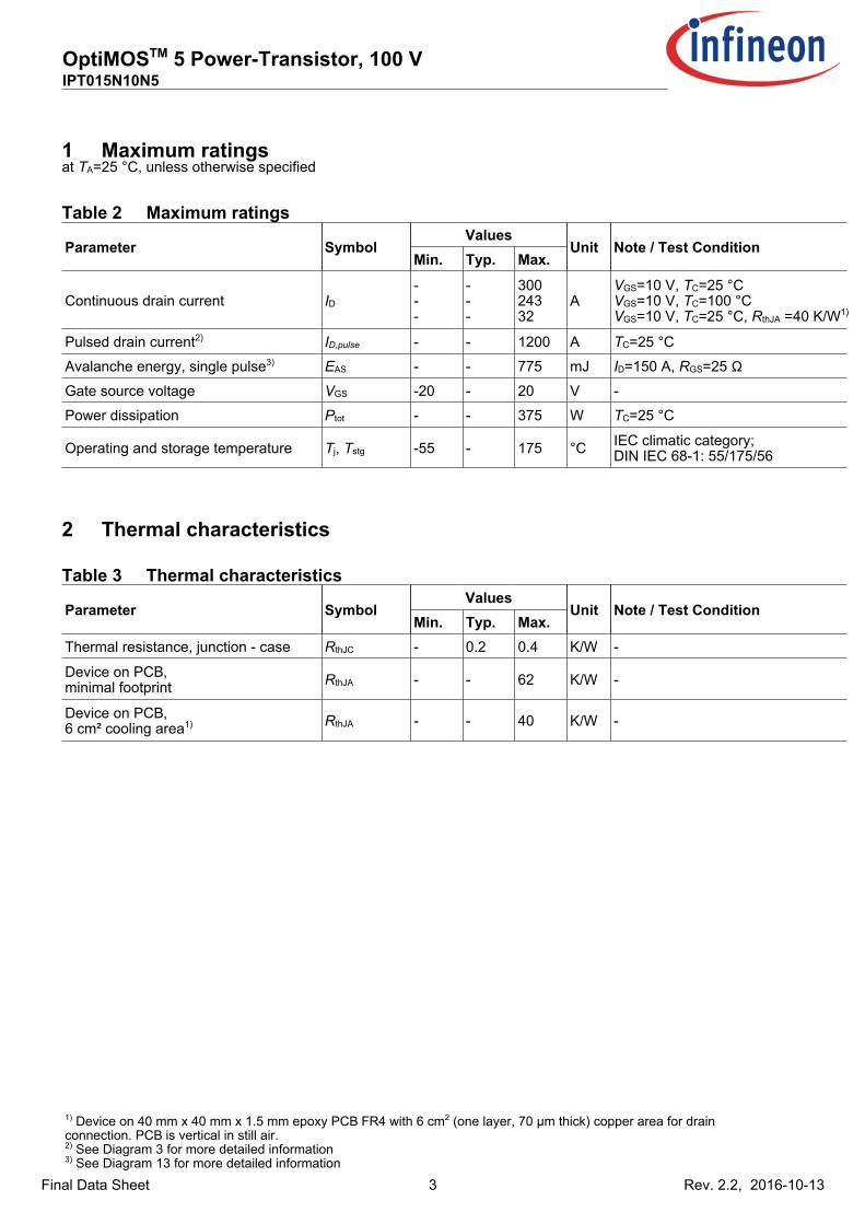
1MaximumratingsatTA=25°C,unlessotherwisespecified
Table2MaximumratingsValues
Min. Typ. Max.Parameter Symbol Unit Note/TestCondition
Continuous drain current ID---
---
30024332
AVGS=10V,TC=25°CVGS=10V,TC=100°CVGS=10V,TC=25°C,RthJA=40K/W1)
Pulsed drain current2) ID,pulse - - 1200 A TC=25°C
Avalanche energy, single pulse3) EAS - - 775 mJ ID=150A,RGS=25Ω
Gate source voltage VGS -20 - 20 V -
Power dissipation Ptot - - 375 W TC=25°C
Operating and storage temperature Tj,Tstg -55 - 175 °C IEC climatic category;DIN IEC 68-1: 55/175/56
2Thermalcharacteristics
Table3ThermalcharacteristicsValues
Min. Typ. Max.Parameter Symbol Unit Note/TestCondition
Thermal resistance, junction - case RthJC - 0.2 0.4 K/W -
Device on PCB,minimal footprint RthJA - - 62 K/W -
Device on PCB,6 cm² cooling area1) RthJA - - 40 K/W -
1) Device on 40 mm x 40 mm x 1.5 mm epoxy PCB FR4 with 6 cm2 (one layer, 70 µm thick) copper area for drainconnection. PCB is vertical in still air.2) See Diagram 3 for more detailed information3) See Diagram 13 for more detailed information

4
OptiMOSTM5Power-Transistor,100VIPT015N10N5
Rev.2.2,2016-10-13Final Data Sheet
3Electricalcharacteristics
Table4StaticcharacteristicsValues
Min. Typ. Max.Parameter Symbol Unit Note/TestCondition
Drain-source breakdown voltage V(BR)DSS 100 - - V VGS=0V,ID=1mA
Gate threshold voltage VGS(th) 2.2 3.0 3.8 V VDS=VGS,ID=280µA
Zero gate voltage drain current IDSS --
0.110
5100 µA VDS=100V,VGS=0V,Tj=25°C
VDS=100V,VGS=0V,Tj=125°C
Gate-source leakage current IGSS - 10 100 nA VGS=20V,VDS=0V
Drain-source on-state resistance RDS(on)--
1.31.6
1.52.0 mΩ VGS=10V,ID=150A
VGS=6V,ID=75A
Gate resistance1) RG - 1.4 2.1 Ω -
Transconductance gfs 140 280 - S |VDS|>2|ID|RDS(on)max,ID=100A
Table5Dynamiccharacteristics1)Values
Min. Typ. Max.Parameter Symbol Unit Note/TestCondition
Input capacitance Ciss - 12000 16000 pF VGS=0V,VDS=50V,f=1MHz
Output capacitance Coss - 1800 2300 pF VGS=0V,VDS=50V,f=1MHz
Reverse transfer capacitance Crss - 80 140 pF VGS=0V,VDS=50V,f=1MHz
Turn-on delay time td(on) - 36 - ns VDD=50V,VGS=10V,ID=100A,RG,ext=1.8Ω
Rise time tr - 30 - ns VDD=50V,VGS=10V,ID=100A,RG,ext=1.8Ω
Turn-off delay time td(off) - 85 - ns VDD=50V,VGS=10V,ID=100A,RG,ext=1.8Ω
Fall time tf - 30 - ns VDD=50V,VGS=10V,ID=100A,RG,ext=1.8Ω
Table6Gatechargecharacteristics2)Values
Min. Typ. Max.Parameter Symbol Unit Note/TestCondition
Gate to source charge Qgs - 53 - nC VDD=50V,ID=100A,VGS=0to10V
Gate charge at threshold Qg(th) - 36 - nC VDD=50V,ID=100A,VGS=0to10V
Gate to drain charge1) Qgd - 34 51 nC VDD=50V,ID=100A,VGS=0to10V
Switching charge Qsw - 51 - nC VDD=50V,ID=100A,VGS=0to10V
Gate charge total1) Qg - 169 211 nC VDD=50V,ID=100A,VGS=0to10V
Gate plateau voltage Vplateau - 4.4 - V VDD=50V,ID=100A,VGS=0to10V
Gate charge total, sync. FET Qg(sync) - 146 - nC VDS=0.1V,VGS=0to10V
Output charge1) Qoss - 213 284 nC VDD=50V,VGS=0V
1) Defined by design. Not subject to production test.2) See ″Gate charge waveforms″ for parameter definition

5
OptiMOSTM5Power-Transistor,100VIPT015N10N5
Rev.2.2,2016-10-13Final Data Sheet
Table7ReversediodeValues
Min. Typ. Max.Parameter Symbol Unit Note/TestCondition
Diode continuous forward current IS - - 300 A TC=25°C
Diode pulse current IS,pulse - - 1200 A TC=25°C
Diode forward voltage VSD - 0.9 1.2 V VGS=0V,IF=100A,Tj=25°C
Reverse recovery time1) trr - 103 206 ns VR=50V,IF=100A,diF/dt=100A/µs
Reverse recovery charge1) Qrr - 316 632 nC VR=50V,IF=100A,diF/dt=100A/µs
1) Defined by design. Not subject to production test.

6
OptiMOSTM5Power-Transistor,100VIPT015N10N5
Rev.2.2,2016-10-13Final Data Sheet
4Electricalcharacteristicsdiagrams
Diagram1:Powerdissipation
TC[°C]
Ptot[W
]
0 25 50 75 100 125 150 1750
50
100
150
200
250
300
350
400
Ptot=f(TC)
Diagram2:Draincurrent
TC[°C]
ID[A
]
0 25 50 75 100 125 150 175 2000
50
100
150
200
250
300
350
ID=f(TC);VGS≥10V
Diagram3:Safeoperatingarea
VDS[V]
ID[A
]
10-1 100 101 102 10310-1
100
101
102
103
104
1 µs
10 µs
100 µs
1 ms
10 msDC
ID=f(VDS);TC=25°C;D=0;parameter:tp
Diagram4:Max.transientthermalimpedance
tp[s]
ZthJC[K
/W]
10-6 10-5 10-4 10-3 10-2 10-1 10010-3
10-2
10-1
100
0.5
0.2
0.1
0.05
0.02
0.01
single pulse
ZthJC=f(tp);parameter:D=tp/T
7
OptiMOSTM5Power-Transistor,100VIPT015N10N5
Rev.2.2,2016-10-13Final Data Sheet
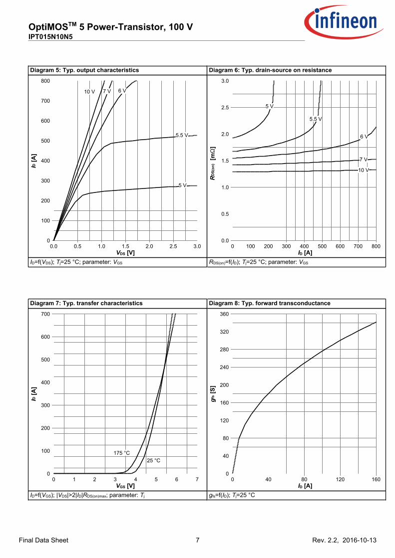
Diagram5:Typ.outputcharacteristics
VDS[V]
ID[A
]
0.0 0.5 1.0 1.5 2.0 2.5 3.00
100
200
300
400
500
600
700
800
7 V10 V 6 V
5.5 V
5 V
ID=f(VDS);Tj=25°C;parameter:VGS
Diagram6:Typ.drain-sourceonresistance
ID[A]
RDS(on
) [m
Ω]
0 100 200 300 400 500 600 700 8000.0
0.5
1.0
1.5
2.0
2.5
3.0
5 V
5.5 V
6 V
7 V
10 V
RDS(on)=f(ID);Tj=25°C;parameter:VGS
Diagram7:Typ.transfercharacteristics
VGS[V]
ID[A
]
0 1 2 3 4 5 6 70
100
200
300
400
500
600
700
175 °C
25 °C
ID=f(VGS);|VDS|>2|ID|RDS(on)max;parameter:Tj
Diagram8:Typ.forwardtransconductance
ID[A]
gfs [S]
0 40 80 120 1600
40
80
120
160
200
240
280
320
360
gfs=f(ID);Tj=25°C

8
OptiMOSTM5Power-Transistor,100VIPT015N10N5
Rev.2.2,2016-10-13Final Data Sheet
Diagram9:Drain-sourceon-stateresistance
Tj[°C]
RDS(on
) [m
Ω]
-60 -20 20 60 100 140 1800.0
0.5
1.0
1.5
2.0
2.5
3.0
3.5
max
typ
RDS(on)=f(Tj);ID=150A;VGS=10V
Diagram10:Typ.gatethresholdvoltage
Tj[°C]
VGS(th) [V]
-60 -20 20 60 100 140 1800
1
2
3
4
2800 µA
280 µA
VGS(th)=f(Tj);VGS=VDS
Diagram11:Typ.capacitances
VDS[V]
C[p
F]
0 20 40 60 80 100101
102
103
104
105
Ciss
Coss
Crss
C=f(VDS);VGS=0V;f=1MHz
Diagram12:Forwardcharacteristicsofreversediode
VSD[V]
IF [A]
0.0 0.5 1.0 1.5 2.0 2.5100
101
102
103
104
25 °C175 °C175°C max25°C max
IF=f(VSD);parameter:Tj

9
OptiMOSTM5Power-Transistor,100VIPT015N10N5
Rev.2.2,2016-10-13Final Data Sheet
Diagram13:Avalanchecharacteristics
tAV[µs]
IAV [A]
100 101 102 103100
101
102
103
25 °C
100 °C
125 °C
IAS=f(tAV);RGS=25Ω;parameter:Tj(start)
Diagram14:Typ.gatecharge
Qgate[nC]
VGS [V]
0 50 100 150 2000
1
2
3
4
5
6
7
8
9
10
80 V
50 V
20 V
VGS=f(Qgate);ID=100Apulsed;parameter:VDD
Diagram15:Drain-sourcebreakdownvoltage
Tj[°C]
VBR(DSS
) [V]
-60 -20 20 60 100 140 18094
96
98
100
102
104
106
108
110
VBR(DSS)=f(Tj);ID=1mA
Gate charge waveforms

10
OptiMOSTM5Power-Transistor,100VIPT015N10N5
Rev.2.2,2016-10-13Final Data Sheet
5PackageOutlines
Z8B00169619
REVISION
ISSUE DATE
EUROPEAN PROJECTION
02
20-02-2014
DOCUMENT NO.
E5
E4
K1
e
MILLIMETERS
A
DIM
MIN MAX
INCHES
MIN MAX
b1
c
D
D2
E
E1
N
L
2.20 2.40 0.087 0.094
9.70
0.40
10.28
9.70
1.60
9.90
0.60
10.58
10.10
2.10
0.382
0.016
0.405
0.382
0.063
0.390
0.024
0.416
0.398
0.083
8 8
1.20 (BSC) 0.047 (BSC)
b 0.70 0.90 0.028 0.035
1) partially covered with Mold Flash
b2 0.42 0.50 0.017 0.020
H
H1
11.48 11.88 0.452 0.468
H2 7.15 0.281
H3 3.59 0.141
H4 3.26 0.128
L1 0.70 0.028
3.30 0.130
7.50 0.295
8.50 0.335
9.46 0.372
6.55 6.75 0.258 0.266
4.18 0.165
L4 1.00 1.30 0.039 0.051
L2 0.60 0.024
2
SCALE
0
4mm
0
2
Figure1OutlinePG-HSOF-8

11
OptiMOSTM5Power-Transistor,100VIPT015N10N5
Rev.2.2,2016-10-13Final Data Sheet
RevisionHistoryIPT015N10N5
Revision:2016-10-13,Rev.2.2
Previous Revision
Revision Date Subjects (major changes since last revision)
2.0 2014-12-17 Release of final version
2.1 2015-02-23 Correction of SOA area with Ipulse = 1200A
2.2 2016-10-13 Update Avalanche Energy
TrademarksofInfineonTechnologiesAG
AURIX™,C166™,CanPAK™,CIPOS™,CoolGaN™,CoolMOS™,CoolSET™,CoolSiC™,CORECONTROL™,CROSSAVE™,DAVE™,DI-POL™,DrBlade™,EasyPIM™,EconoBRIDGE™,EconoDUAL™,EconoPACK™,EconoPIM™,EiceDRIVER™,eupec™,FCOS™,HITFET™,HybridPACK™,Infineon™,ISOFACE™,IsoPACK™,i-Wafer™,MIPAQ™,ModSTACK™,my-d™,NovalithIC™,OmniTune™,OPTIGA™,OptiMOS™,ORIGA™,POWERCODE™,PRIMARION™,PrimePACK™,PrimeSTACK™,PROFET™,PRO-SIL™,RASIC™,REAL3™,ReverSave™,SatRIC™,SIEGET™,SIPMOS™,SmartLEWIS™,SOLIDFLASH™,SPOC™,TEMPFET™,thinQ™,TRENCHSTOP™,TriCore™.
TrademarksupdatedAugust2015
OtherTrademarks
Allreferencedproductorservicenamesandtrademarksarethepropertyoftheirrespectiveowners.
WeListentoYourCommentsAnyinformationwithinthisdocumentthatyoufeeliswrong,unclearormissingatall?Yourfeedbackwillhelpustocontinuouslyimprovethequalityofthisdocument.Pleasesendyourproposal(includingareferencetothisdocument)to:[email protected]
PublishedbyInfineonTechnologiesAG81726München,Germany©2016InfineonTechnologiesAGAllRightsReserved.
LegalDisclaimerTheinformationgiveninthisdocumentshallinnoeventberegardedasaguaranteeofconditionsorcharacteristics(“Beschaffenheitsgarantie”).
Withrespecttoanyexamples,hintsoranytypicalvaluesstatedhereinand/oranyinformationregardingtheapplicationoftheproduct,InfineonTechnologiesherebydisclaimsanyandallwarrantiesandliabilitiesofanykind,includingwithoutlimitationwarrantiesofnon-infringementofintellectualpropertyrightsofanythirdparty.Inaddition,anyinformationgiveninthisdocumentissubjecttocustomer’scompliancewithitsobligationsstatedinthisdocumentandanyapplicablelegalrequirements,normsandstandardsconcerningcustomer’sproductsandanyuseoftheproductofInfineonTechnologiesincustomer’sapplications.Thedatacontainedinthisdocumentisexclusivelyintendedfortechnicallytrainedstaff.Itistheresponsibilityofcustomer’stechnicaldepartmentstoevaluatethesuitabilityoftheproductfortheintendedapplicationandthecompletenessoftheproductinformationgiveninthisdocumentwithrespecttosuchapplication.
InformationForfurtherinformationontechnology,deliverytermsandconditionsandpricespleasecontactyournearestInfineonTechnologiesOffice(www.infineon.com).
WarningsDuetotechnicalrequirements,componentsmaycontaindangeroussubstances.Forinformationonthetypesinquestion,pleasecontactthenearestInfineonTechnologiesOffice.TheInfineonTechnologiescomponentdescribedinthisDataSheetmaybeusedinlife-supportdevicesorsystemsand/orautomotive,aviationandaerospaceapplicationsorsystemsonlywiththeexpresswrittenapprovalofInfineonTechnologies,ifafailureofsuchcomponentscanreasonablybeexpectedtocausethefailureofthatlife-support,automotive,aviationandaerospacedeviceorsystemortoaffectthesafetyoreffectivenessofthatdeviceorsystem.Lifesupportdevicesorsystemsareintendedtobeimplantedinthehumanbodyortosupportand/ormaintainandsustainand/orprotecthumanlife.Iftheyfail,itisreasonabletoassumethatthehealthoftheuserorotherpersonsmaybeendangered.