Embed Size (px)
Citation preview

Edition 2014-03-06
Published by Infineon Technologies AG,
81726 Munich, Germany.
© 2014 Infineon Technologies AG
All Rights Reserved.
LEGAL DISCLAIMER
THE INFORMATION GIVEN IN THIS APPLICATION NOTE IS GIVEN AS A HINT FOR THEIMPLEMENTATION OF THE INFINEON TECHNOLOGIES COMPONENT ONLY AND SHALL NOT BEREGARDED AS ANY DESCRIPTION OR WARRANTY OF A CERTAIN FUNCTIONALITY, CONDITION ORQUALITY OF THE INFINEON TECHNOLOGIES COMPONENT. THE RECIPIENT OF THIS APPLICATIONNOTE MUST VERIFY ANY FUNCTION DESCRIBED HEREIN IN THE REAL APPLICATION. INFINEONTECHNOLOGIES HEREBY DISCLAIMS ANY AND ALL WARRANTIES AND LIABILITIES OF ANY KIND(INCLUDING WITHOUT LIMITATION WARRANTIES OF NON-INFRINGEMENT OF INTELLECTUALPROPERTY RIGHTS OF ANY THIRD PARTY) WITH RESPECT TO ANY AND ALL INFORMATION GIVEN INTHIS APPLICATION NOTE.
Information
For further information on technology, delivery terms and conditions and prices, please contact the nearestInfineon Technologies Office (www.infineon.com).
Warnings
Due to technical requirements, components may contain dangerous substances. For information on the types inquestion, please contact the nearest Infineon Technologies Office.
Infineon Technologies components may be used in life-support devices or systems only with the express writtenapproval of Infineon Technologies, if a failure of such components can reasonably be expected to cause thefailure of that life-support device or system or to affect the safety or effectiveness of that device or system. Lifesupport devices or systems are intended to be implanted in the human body or to support and/or maintain andsustain and/or protect human life. If they fail, it is reasonable to assume that the health of the user or otherpersons may be endangered.
Quasi-Resonant PWM controllerICE2QS03G
Data Sheet 3 V2.3, 2014-03-06
Trademarks of Infineon Technologies AG
AURIX™, C166™, CanPAK™, CIPOS™, CIPURSE™, EconoPACK™, CoolMOS™, CoolSET™,CORECONTROL™, CROSSAVE™, DAVE™, DI-POL™, EasyPIM™, EconoBRIDGE™, EconoDUAL™,EconoPIM™, EconoPACK™, EiceDRIVER™, eupec™, FCOS™, HITFET™, HybridPACK™, I²RF™,ISOFACE™, IsoPACK™, MIPAQ™, ModSTACK™, my-d™, NovalithIC™, OptiMOS™, ORIGA™,POWERCODE™; PRIMARION™, PrimePACK™, PrimeSTACK™, PRO-SIL™, PROFET™, RASIC™,ReverSave™, SatRIC™, SIEGET™, SINDRION™, SIPMOS™, SmartLEWIS™, SOLID FLASH™,TEMPFET™, thinQ!™, TRENCHSTOP™, TriCore™.
Other Trademarks
Advance Design System™ (ADS) of Agilent Technologies, AMBA™, ARM™, MULTI-ICE™, KEIL™,PRIMECELL™, REALVIEW™, THUMB™, µVision™ of ARM Limited, UK. AUTOSAR™ is licensed byAUTOSAR development partnership. Bluetooth™ of Bluetooth SIG Inc. CAT-iq™ of DECT Forum.COLOSSUS™, FirstGPS™ of Trimble Navigation Ltd. EMV™ of EMVCo, LLC (Visa Holdings Inc.). EPCOS™of Epcos AG. FLEXGO™ of Microsoft Corporation. FlexRay™ is licensed by FlexRay Consortium.HYPERTERMINAL™ of Hilgraeve Incorporated. IEC™ of Commission Electrotechnique Internationale. IrDA™of Infrared Data Association Corporation. ISO™ of INTERNATIONAL ORGANIZATION FORSTANDARDIZATION. MATLAB™ of MathWorks, Inc. MAXIM™ of Maxim Integrated Products, Inc.MICROTEC™, NUCLEUS™ of Mentor Graphics Corporation. MIPI™ of MIPI Alliance, Inc. MIPS™ of MIPSTechnologies, Inc., USA. muRata™ of MURATA MANUFACTURING CO., MICROWAVE OFFICE™ (MWO) ofApplied Wave Research Inc., OmniVision™ of OmniVision Technologies, Inc. Openwave™ Openwave SystemsInc. RED HAT™ Red Hat, Inc. RFMD™ RF Micro Devices, Inc. SIRIUS™ of Sirius Satellite Radio Inc.SOLARIS™ of Sun Microsystems, Inc. SPANSION™ of Spansion LLC Ltd. Symbian™ of Symbian SoftwareLimited. TAIYO YUDEN™ of Taiyo Yuden Co. TEAKLITE™ of CEVA, Inc. TEKTRONIX™ of Tektronix Inc.TOKO™ of TOKO KABUSHIKI KAISHA TA. UNIX™ of X/Open Company Limited. VERILOG™, PALLADIUM™of Cadence Design Systems, Inc. VLYNQ™ of Texas Instruments Incorporated. VXWORKS™, WIND RIVER™of WIND RIVER SYSTEMS, INC. ZETEX™ of Diodes Zetex Limited.
Last Trademarks Update 2011-11-11
Quasi-Resonant PWM controllerICE2QS03G
Data Sheet 4 V2.3, 2014-03-06
Revision History
Major changes since previous revision
Date Version Changed By Change Description
2014-03-06 2.3 Added VVCCPD, and marking drawing.Removed VOUT. Revised typo, IVCCcharge1,IVCCcharge2, IZCMAX, outline dimensiondrawing and upgrade to -40°C operatingtemperature
We Listen to Your Comments
Is there any information in this document that you feel is wrong, unclear or missing?Your feedback will help us to continuously improve the quality of our documentation.Please send your proposal (including a reference to this document title/number) to:
Quasi-Resonant PWM controllerICE2QS03G
Data Sheet 5 V2.3, 2014-03-06
Table of Contents
Revision History...................................................................................................................................................4
Table of Contents .................................................................................................................................................5
1 Pin Configuration and Functionality ..............................................................................................7
1.1 Pin Configuration with PG-DSO-8......................................................................................................7
1.2 Pin Functionality.................................................................................................................................7
2 Representative Block Diagram .......................................................................................................8
3 Functional Description ....................................................................................................................9
3.1 VCC Pre-Charging and Typical VCC Voltage During Start-up...........................................................9
3.2 Soft-start ............................................................................................................................................9
3.3 Normal Operation.............................................................................................................................10
3.3.1 Digital Frequency Reduction.......................................................................................................10
3.3.1.1 Up/down counter....................................................................................................................10
3.3.1.2 Zero crossing (ZC counter) ....................................................................................................11
3.3.2 Ringing suppression time............................................................................................................12
3.3.2.1 Switch on determination ........................................................................................................12
3.3.3 Switch Off Determination ............................................................................................................12
3.3.4 Modulated gate drive ..................................................................................................................12
3.4 Current Limitation.............................................................................................................................13
3.4.1 Foldback Point Correction...........................................................................................................13
3.5 Active Burst Mode Operation ...........................................................................................................14
3.5.1 Entering Active Burst Mode Operation........................................................................................14
3.5.2 During Active Burst Mode Operation ..........................................................................................14
3.5.3 Leaving Active Burst Mode Operation ........................................................................................15
3.6 Protection Functions ........................................................................................................................16
4 Electrical Characteristics ..............................................................................................................17
4.1 Absolute Maximum Ratings .............................................................................................................17
4.2 Operating Range..............................................................................................................................17
4.3 Characteristics .................................................................................................................................18
4.3.1 Supply Section............................................................................................................................18
4.3.2 Internal Voltage Reference .........................................................................................................18
4.3.3 PWM Section ..............................................................................................................................19
4.3.4 Current Sense.............................................................................................................................19
4.3.5 Soft Start .....................................................................................................................................19
4.3.6 Foldback Point Correction...........................................................................................................19
4.3.7 Digital Zero Crossing ..................................................................................................................20
4.3.8 Active Burst Mode.......................................................................................................................20
4.3.9 Protection....................................................................................................................................21
4.3.10 Gate Drive...................................................................................................................................21
5 Outline Dimension .........................................................................................................................22
6 Marking ...........................................................................................................................................23
Quasi-Resonant PWM controllerICE2QS03G
Data Sheet 6 V2.3, 2014-03-06
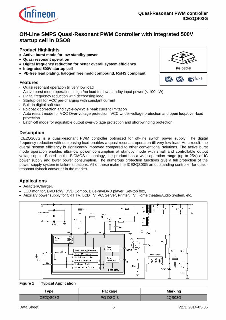
Off-Line SMPS Quasi-Resonant PWM Controller with integrated 500Vstartup cell in DSO8
Product Highlights Active burst mode for low standby power Quasi resonant operation Digital frequency reduction for better overall system efficiency Integrated 500V startup cell Pb-free lead plating, halogen free mold compound, RoHS compliant
Features• Quasi resonant operation till very low load• Active burst mode operation at light/no load for low standby input power (< 100mW)• Digital frequency reduction with decreasing load• Startup cell for VCC pre-charging with constant current• Built-in digital soft-start• Foldback correction and cycle-by-cycle peak current limitation• Auto restart mode for VCC Over-voltage protection, VCC Under-voltage protection and open loop/over-load
protection• Latch-off mode for adjustable output over-voltage protection and short-winding protection
DescriptionICE2QS03G is a quasi-resonant PWM controller optimized for off-line switch power supply. The digitalfrequency reduction with decreasing load enables a quasi-resonant operation till very low load. As a result, theoverall system efficiency is significantly improved compared to other conventional solutions. The active burstmode operation enables ultra-low power consumption at standby mode with small and controllable outputvoltage ripple. Based on the BiCMOS technology, the product has a wide operation range (up to 25V) of ICpower supply and lower power consumption. The numerous protection functions give a full protection of thepower supply system in failure situations. All of these make the ICE2QS03G an outstanding controller for quasi-resonant flyback converter in the market.
Applications Adapter/Charger,
LCD monitor, DVD R/W, DVD Combo, Blue-ray/DVD player, Set-top box, Auxiliary power supply for CRT TV, LCD TV, PC, Server, Printer, TV, Home theater/Audio System, etc.
Figure 1 Typical Application
Type Package Marking
ICE2QS03G PG-DSO-8 2QS03G
PG-DSO-8
Quasi-Resonant PWM controllerICE2QS03G
Pin Configuration and Functionality
Data Sheet 7 V2.3, 2014-03-06
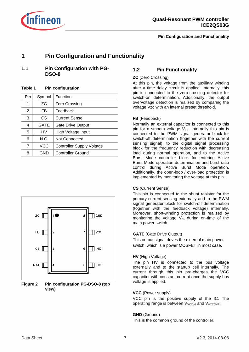
1 Pin Configuration and Functionality
1.1 Pin Configuration with PG-DSO-8
Table 1 Pin configuration
Pin Symbol Function
1 ZC Zero Crossing
2 FB Feedback
3 CS Current Sense
4 GATE Gate Drive Output
5 HV High Voltage input
6 N.C. Not Connected
7 VCC Controller Supply Voltage
8 GND Controller Ground
Figure 2 Pin configuration PG-DSO-8 (topview)
1.2 Pin Functionality
ZC (Zero Crossing)
At this pin, the voltage from the auxiliary windingafter a time delay circuit is applied. Internally, thispin is connected to the zero-crossing detector forswitch-on determination. Additionally, the outputovervoltage detection is realized by comparing thevoltage Vzc with an internal preset threshold.
FB (Feedback)
Normally an external capacitor is connected to thispin for a smooth voltage VFB. Internally this pin isconnected to the PWM signal generator block forswitch-off determination (together with the currentsensing signal), to the digital signal processingblock for the frequency reduction with decreasingload during normal operation, and to the ActiveBurst Mode controller block for entering ActiveBurst Mode operation determination and burst ratiocontrol during Active Burst Mode operation.Additionally, the open-loop / over-load protection isimplemented by monitoring the voltage at this pin.
CS (Current Sense)
This pin is connected to the shunt resistor for theprimary current sensing externally and to the PWMsignal generator block for switch-off determination(together with the feedback voltage) internally.Moreover, short-winding protection is realized bymonitoring the voltage Vcs during on-time of themain power switch.
GATE (Gate Drive Output)
This output signal drives the external main power
switch, which is a power MOSFET in most case.
HV (High Voltage)
The pin HV is connected to the bus voltageexternally and to the startup cell internally. Thecurrent through this pin pre-charges the VCCcapacitor with constant current once the supply busvoltage is applied.
VCC (Power supply)
VCC pin is the positive supply of the IC. Theoperating range is between VVCCoff and VVCCOVP.
GND (Ground)
This is the common ground of the controller.
Quasi-Resonant PWM controllerICE2QS03G
Representative Block Diagram
Data Sheet 8 V2.3, 2014-03-06
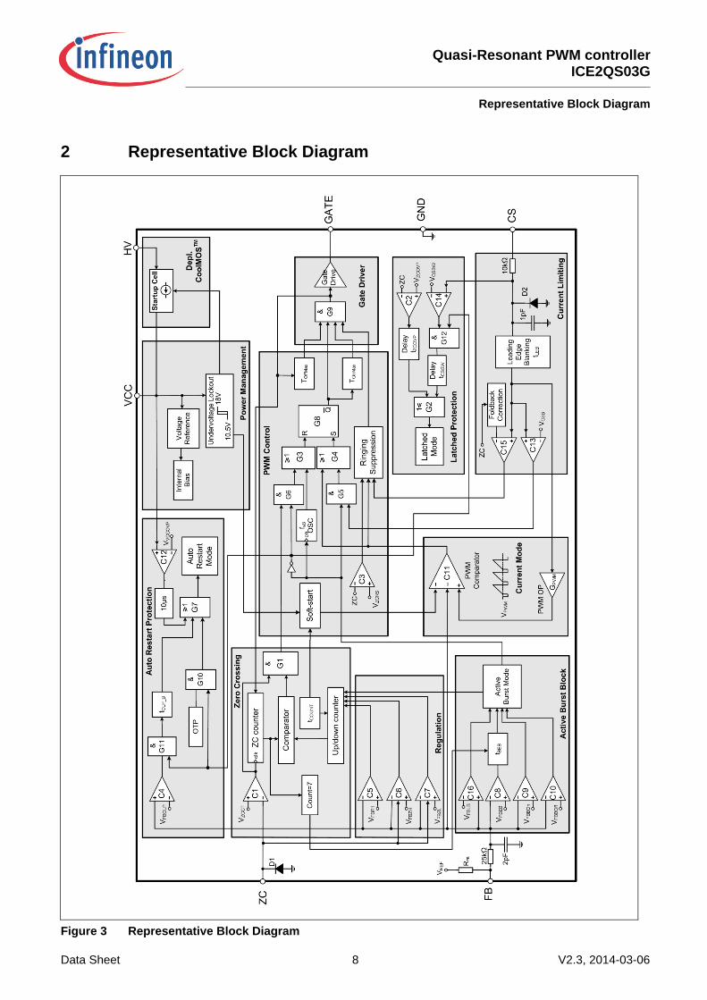
2 Representative Block Diagram
Figure 3 Representative Block Diagram
Quasi-Resonant PWM controllerICE2QS03G
Functional Description
Data Sheet 9 V2.3, 2014-03-06
3 Functional Description
3.1 VCC Pre-Charging and Typical VCC Voltage During Start-up
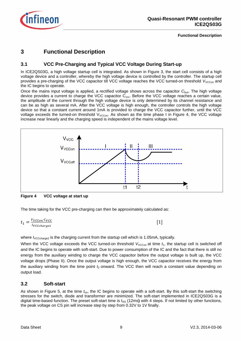
In ICE2QS03G, a high voltage startup cell is integrated. As shown in Figure 3, the start cell consists of a highvoltage device and a controller, whereby the high voltage device is controlled by the controller. The startup cellprovides a pre-charging of the VCC capacitor till VCC voltage reaches the VCC turned-on threshold VVCCon andthe IC begins to operate.
Once the mains input voltage is applied, a rectified voltage shows across the capacitor Cbus. The high voltagedevice provides a current to charge the VCC capacitor Cvcc. Before the VCC voltage reaches a certain value,the amplitude of the current through the high voltage device is only determined by its channel resistance andcan be as high as several mA. After the VCC voltage is high enough, the controller controls the high voltagedevice so that a constant current around 1mA is provided to charge the VCC capacitor further, until the VCCvoltage exceeds the turned-on threshold VVCCon. As shown as the time phase I in Figure 4, the VCC voltageincrease near linearly and the charging speed is independent of the mains voltage level.
Figure 4 VCC voltage at start up
The time taking for the VCC pre-charging can then be approximately calculated as:
where IVCCcharge2 is the charging current from the startup cell which is 1.05mA, typically.
When the VCC voltage exceeds the VCC turned-on threshold VVCCon at time t1, the startup cell is switched off
and the IC begins to operate with soft-start. Due to power consumption of the IC and the fact that there is still no
energy from the auxiliary winding to charge the VCC capacitor before the output voltage is built up, the VCC
voltage drops (Phase II). Once the output voltage is high enough, the VCC capacitor receives the energy from
the auxiliary winding from the time point t2 onward. The VCC then will reach a constant value depending on
output load.
3.2 Soft-start
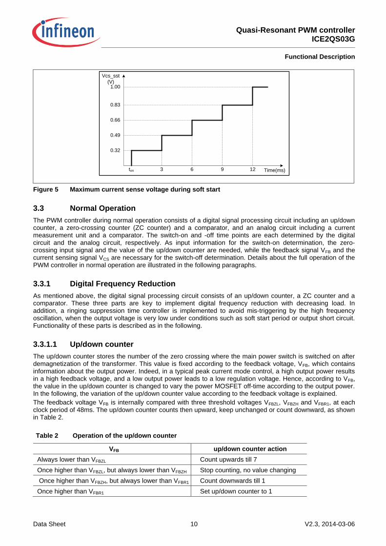
As shown in Figure 5, at the time ton, the IC begins to operate with a soft-start. By this soft-start the switchingstresses for the switch, diode and transformer are minimized. The soft-start implemented in ICE2QS03G is adigital time-based function. The preset soft-start time is tSS (12ms) with 4 steps. If not limited by other functions,the peak voltage on CS pin will increase step by step from 0.32V to 1V finally.
Quasi-Resonant PWM controllerICE2QS03G
Functional Description
Data Sheet 10 V2.3, 2014-03-06
ton 3 6 9 12
0.32
0.49
0.66
0.83
1.00
Vcs_sst(V)
Time(ms)
Figure 5 Maximum current sense voltage during soft start
3.3 Normal Operation
The PWM controller during normal operation consists of a digital signal processing circuit including an up/downcounter, a zero-crossing counter (ZC counter) and a comparator, and an analog circuit including a currentmeasurement unit and a comparator. The switch-on and -off time points are each determined by the digitalcircuit and the analog circuit, respectively. As input information for the switch-on determination, the zero-crossing input signal and the value of the up/down counter are needed, while the feedback signal VFB and thecurrent sensing signal VCS are necessary for the switch-off determination. Details about the full operation of thePWM controller in normal operation are illustrated in the following paragraphs.
3.3.1 Digital Frequency Reduction
As mentioned above, the digital signal processing circuit consists of an up/down counter, a ZC counter and acomparator. These three parts are key to implement digital frequency reduction with decreasing load. Inaddition, a ringing suppression time controller is implemented to avoid mis-triggering by the high frequencyoscillation, when the output voltage is very low under conditions such as soft start period or output short circuit.Functionality of these parts is described as in the following.
3.3.1.1 Up/down counter
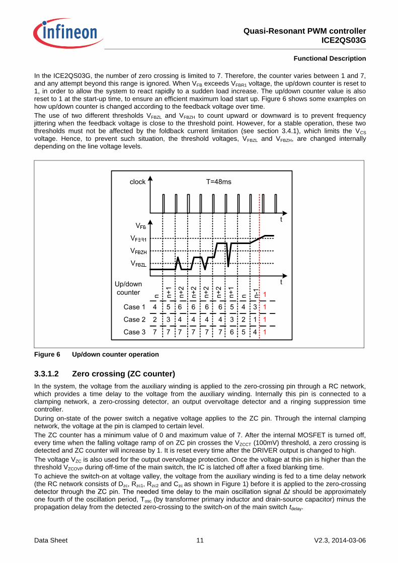
The up/down counter stores the number of the zero crossing where the main power switch is switched on afterdemagnetization of the transformer. This value is fixed according to the feedback voltage, VFB, which containsinformation about the output power. Indeed, in a typical peak current mode control, a high output power resultsin a high feedback voltage, and a low output power leads to a low regulation voltage. Hence, according to VFB,the value in the up/down counter is changed to vary the power MOSFET off-time according to the output power.In the following, the variation of the up/down counter value according to the feedback voltage is explained.
The feedback voltage VFB is internally compared with three threshold voltages VFBZL, VFBZH and VFBR1, at eachclock period of 48ms. The up/down counter counts then upward, keep unchanged or count downward, as shownin Table 2.
Table 2 Operation of the up/down counter
VFB up/down counter action
Always lower than VFBZL Count upwards till 7
Once higher than VFBZL, but always lower than VFBZH Stop counting, no value changing
Once higher than VFBZH, but always lower than VFBR1 Count downwards till 1
Once higher than VFBR1 Set up/down counter to 1
Quasi-Resonant PWM controllerICE2QS03G
Functional Description
Data Sheet 11 V2.3, 2014-03-06
In the ICE2QS03G, the number of zero crossing is limited to 7. Therefore, the counter varies between 1 and 7,and any attempt beyond this range is ignored. When VFB exceeds VFBR1 voltage, the up/down counter is reset to1, in order to allow the system to react rapidly to a sudden load increase. The up/down counter value is alsoreset to 1 at the start-up time, to ensure an efficient maximum load start up. Figure 6 shows some examples onhow up/down counter is changed according to the feedback voltage over time.
The use of two different thresholds VFBZL and VFBZH to count upward or downward is to prevent frequencyjittering when the feedback voltage is close to the threshold point. However, for a stable operation, these twothresholds must not be affected by the foldback current limitation (see section 3.4.1), which limits the VCS
voltage. Hence, to prevent such situation, the threshold voltages, VFBZL and VFBZH, are changed internallydepending on the line voltage levels.
Figure 6 Up/down counter operation
3.3.1.2 Zero crossing (ZC counter)
In the system, the voltage from the auxiliary winding is applied to the zero-crossing pin through a RC network,which provides a time delay to the voltage from the auxiliary winding. Internally this pin is connected to aclamping network, a zero-crossing detector, an output overvoltage detector and a ringing suppression timecontroller.
During on-state of the power switch a negative voltage applies to the ZC pin. Through the internal clampingnetwork, the voltage at the pin is clamped to certain level.
The ZC counter has a minimum value of 0 and maximum value of 7. After the internal MOSFET is turned off,every time when the falling voltage ramp of on ZC pin crosses the VZCCT (100mV) threshold, a zero crossing isdetected and ZC counter will increase by 1. It is reset every time after the DRIVER output is changed to high.
The voltage VZC is also used for the output overvoltage protection. Once the voltage at this pin is higher than thethreshold VZCOVP during off-time of the main switch, the IC is latched off after a fixed blanking time.
To achieve the switch-on at voltage valley, the voltage from the auxiliary winding is fed to a time delay network(the RC network consists of Dzc, Rzc1, Rzc2 and Czc as shown in Figure 1) before it is applied to the zero-crossingdetector through the ZC pin. The needed time delay to the main oscillation signal Δt should be approximatelyone fourth of the oscillation period, Tosc (by transformer primary inductor and drain-source capacitor) minus thepropagation delay from the detected zero-crossing to the switch-on of the main switch tdelay.
Quasi-Resonant PWM controllerICE2QS03G
Functional Description
Data Sheet 12 V2.3, 2014-03-06
This time delay should be matched by adjusting the time constant of the RC network which is calculated as:
3.3.2 Ringing suppression time
After MOSFET is turned off, there will be some oscillation on VDS, which will also appear on the voltage on ZCpin. To avoid mis-triggering by such oscillations to turn on the MOSFET, a ringing suppression timer isimplemented. This suppression time is depended on the voltage VZC. If the voltage VZC is lower than thethreshold VZCRS, a longer preset time tZCRS2 is applied. However, if the voltage VZC is higher than the threshold, ashorter time tZCRS1 is set.
3.3.2.1 Switch on determination
After the gate drive goes to low, it cannot be changed to high during ring suppression time.
After ring suppression time, the gate drive can be turned on when the ZC counter value is higher or equal toup/down counter value.
However, it is also possible that the oscillation between primary inductor and drain-source capacitor damps veryfast and IC cannot detect enough zero crossings and ZC counter value will not be high enough to turn on thegate drive. In this case, a maximum off time is implemented. After gate drive has been remained off for theperiod of TOffMax, the gate drive will be turned on again regardless of the counter values and VZC. This functioncan effectively prevent the switching frequency from going lower than 20kHz. Otherwise it will cause audiblenoise during start up.
3.3.3 Switch Off Determination
In the converter system, the primary current is sensed by an external shunt resistor, which is connectedbetween low-side terminal of the main power switch and the common ground. The sensed voltage across theshunt resistor VCS is applied to an internal current measurement unit, and its output voltage V1 is compared withthe regulation voltage VFB. Once the voltage V1 exceeds the voltage VFB, the output flip-flop is reset. As a result,the main power switch is switched off. The relationship between the V1 and the VCS is described by:
To avoid mis-triggering caused by the voltage spike across the shunt resistor at the turn on of the main power
switch, a leading edge blanking time, tLEB, is applied to the output of the comparator. In other words, once the
gate drive is turned on, the minimum on time of the gate drive is the leading edge blanking time.
In addition, there is a maximum on time, tOnMax, limitation implemented in the IC. Once the gate drive has been
in high state longer than the maximum on time, it will be turned off to prevent the switching frequency from going
too low because of long on time.
3.3.4 Modulated gate drive
The drive-stage is optimized for EMI consideration. The switch on speed is slowed down before it reaches theCoolMOS
TMturn on threshold. That is a slope control of the rising edge at the output of driver (Figure 7). Thus
the leading switch spike during turn on is minimized.
Quasi-Resonant PWM controllerICE2QS03G
Functional Description
Data Sheet 13 V2.3, 2014-03-06
Figure 7 Gate rising waveform
3.4 Current Limitation
There is a cycle by cycle current limitation realized by the current limit comparator to provide an over-currentdetection. The source current of the MOSFET is sensed via a sense resistor RCS. By means of RCS the sourcecurrent is transformed to a sense voltage VCS which is fed into the pin CS. If the voltage VCS exceeds an internalvoltage limit, adjusted according to the Mains voltage, the comparator immediately turns off the gate drive.
To prevent the Current Limitation process from distortions caused by leading edge spikes, a Leading EdgeBlanking time (tLEB) is integrated in the current sensing path.
A further comparator is implemented to detect dangerous current levels (VCSSW) which could occur if one or
more transformer windings are shorted or if the secondary diode is shorted. To avoid an accidental latch off, a
spike blanking time of tCSSW is integrated in the output path of the comparator.
3.4.1 Foldback Point Correction
When the main bus voltage increases, the switch on time becomes shorter and therefore the operatingfrequency is also increased. As a result, for a constant primary current limit, the maximum possible outputpower is increased which is beyond the converter design limit.
To avoid such a situation, the internal foldback point correction circuit varies the VCS voltage limit according tothe bus voltage. This means the VCS will be decreased when the bus voltage increases. To keep a constantmaximum input power of the converter, the required maximum VCS versus various input bus voltage can becalculated, which is shown in Figure 8.
Figure 8 Variation of the VCS limit voltage according to the IZC current
Quasi-Resonant PWM controllerICE2QS03G
Functional Description
Data Sheet 14 V2.3, 2014-03-06
According to the typical application circuit, when MOSFET is turned on, a negative voltage proportional to bus
voltage will be coupled to auxiliary winding. Inside ICE2QS03G, an internal circuit will clamp the voltage on ZCpin to nearly 0V. As a result, the current flowing out from ZC pin can be calculated as
When this current is higher than IZC_FS, the amount of current exceeding this threshold is used togenerate an offset to decrease the maximum limit on VCS. Since the ideal curve shown in Figure 8 is anonlinear one, a digital block in ICE2QS03G is implemented to get a better control of maximumoutput power. Additional advantage to use digital circuit is the production tolerance is smallercompared to analog solutions. The typical maximum limit on VCS versus the ZC current is shown inFigure 9.
Figure 9 VCS-max versus IZC
3.5 Active Burst Mode Operation
At light load condition, the IC enters Active Burst Mode operation to minimize the power consumption. Detailsabout Active Burst Mode operation are explained in the following paragraphs.
3.5.1 Entering Active Burst Mode Operation
For determination of entering Active Burst Mode operation, three conditions apply:
the feedback voltage is lower than the threshold of VFBEB (1.25V). Accordingly, the peak current sensevoltage across the shunt resistor is 0.17V;
the up/down counter is NZC_ABM (7) and a certain blanking time tBEB (24ms).
Once all of these conditions are fulfilled, the Active Burst Mode flip-flop is set and the controller enters ActiveBurst Mode operation. This multi-condition determination for entering Active Burst Mode operation prevents mis-triggering of entering Active Burst Mode operation, so that the controller enters Active Burst Mode operationonly when the output power is really low during the preset blanking time.
3.5.2 During Active Burst Mode Operation
After entering the Active Burst Mode the feedback voltage rises as VOUT starts to decrease due to the inactivePWM section. One comparator observes the feedback signal if the voltage level VFBBOn (3.6V) is exceeded. Inthat case the internal circuit is again activated by the internal bias to start with switching.
Quasi-Resonant PWM controllerICE2QS03G
Functional Description
Data Sheet 15 V2.3, 2014-03-06
Turn-on of the power MOSFET is triggered by the timer. The PWM generator for Active Burst Mode operationcomposes of a timer with a fixed frequency of fsB (52kHz, typical) and an analog comparator. Turn-off is resultedif the voltage across the shunt resistor at CS pin hits the threshold VcsB (0.34V). A turn-off can also be triggeredif the duty ratio exceeds the maximal duty ratio DmaxB (50%). In operation, the output flip-flop will be reset by oneof these signals which come first.
If the output load is still low, the feedback signal decreases as the PWM section is operating. When feedbacksignal reaches the low threshold VFBBOff (3.0V), the internal bias is reset again and the PWM section is disableduntil next time regulation signal increases beyond the VFBBOn (3.6V) threshold. If working in Active Burst Modethe feedback signal is changing like a saw tooth between VFBBOff and VFBBOn shown in Figure 10.
3.5.3 Leaving Active Burst Mode Operation
The feedback voltage immediately increases if there is a high load jump. This is observed by a comparator. Asthe current limit is 34% during Active Burst Mode a certain load is needed so that feedback voltage can exceedVFBLB (4.5V). After leaving active burst mode, maximum current can now be provided to stabilize VO. In addition,the up/down counter will be set to 1 immediately after leaving Active Burst Mode. This is helpful to decrease theoutput voltage undershoot.
Figure 10 Signals in Active Burst Mode
Quasi-Resonant PWM controllerICE2QS03G
Functional Description
Data Sheet 16 V2.3, 2014-03-06
3.6 Protection Functions
The IC provides full protection functions. The following table summarizes these protection functions.
Table 3 Protection features
VCC Over-voltage Auto Restart ModeVCC Under-voltage Auto Restart ModeOver-load/Open Loop Auto Restart ModeOver-temperature Auto Restart ModeOutput Over-voltage Latched Off ModeShort Winding Latched Off Mode
During operation, the VCC voltage is continuously monitored. In case of an under-voltage or an over-voltage,the IC is reset and the main power switch is then kept off. After the VCC voltage falls below the thresholdVVCCoff, the startup cell is activated. The VCC capacitor is then charged up. Once the voltage exceeds thethreshold VVCCon, the IC begins to operate with a new soft-start.
In case of open control loop or output over load, the feedback voltage will be pulled up. After a blanking time oftOLP_B (30ms), the IC enters auto-restart mode. The blanking time here enables the converter to provide a peakpower in case the increase in VFB is due to a sudden load increase. This output over load protection is disabledduring burst mode.
During off-time of the power switch, the voltage at the zero-crossing pin is monitored for output over-voltagedetection. If the voltage is higher than the preset threshold VZCOVP, the IC is latched off after the preset blankingtime tZCOVP. This latch off mode can only be reset if the Vcc < VVCCPD.
If the junction temperature of IC controller exceeds TjCon (130 °C), the IC enters into OTP auto restart mode.This OTP is disabled during burst mode.
If the voltage at the current sensing pin is higher than the preset threshold VCSSW during on-time of the powerswitch, the IC is latched off. This is short-winding protection. The short winding protection is disabled duringburst mode.
During latch-off protection mode, the VCC voltage drops to VVCCoff (10.5V) and then the startup cell is activated.
The VCC voltage is then charged to VVCCon (18V). The startup cell is shut down again. This action repeats again
and again.
There is also a maximum on time limitation implemented inside the ICE2QS03G. Once the gate voltage is high
and longer than tOnMax, the switch is turned off immediately.
Quasi-Resonant PWM controllerICE2QS03G
Electrical Characteristics
Data Sheet 17 V2.3, 2014-03-06
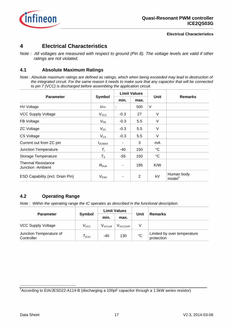
4 Electrical Characteristics
Note : All voltages are measured with respect to ground (Pin 8). The voltage levels are valid if otherratings are not violated.
4.1 Absolute Maximum Ratings
Note : Absolute maximum ratings are defined as ratings, which when being exceeded may lead to destruction ofthe integrated circuit. For the same reason it needs to make sure that any capacitor that will be connectedto pin 7 (VCC) is discharged before assembling the application circuit.
Parameter SymbolLimit Values
Unit Remarksmin. max.
HV Voltage VHV - 500 V
VCC Supply Voltage VVCC -0.3 27 V
FB Voltage VFB -0.3 5.5 V
ZC Voltage VZC -0.3 5.5 V
CS Voltage VCS -0.3 5.5 V
Current out from ZC pin IZCMAX - 3 mA
Junction Temperature Tj -40 150 °C
Storage Temperature TS -55 150 °C
Thermal ResistanceJunction -Ambient
RthJA - 185 K/W
ESD Capability (incl. Drain Pin) VESD - 2 kVHuman bodymodel
1
4.2 Operating Range
Note : Within the operating range the IC operates as described in the functional description.
Parameter SymbolLimit Values
Unit Remarksmin. max.
VCC Supply Voltage VVCC VVCCoff VVCCOVP V
Junction Temperature ofController
TjCon -40 130 °CLimited by over temperatureprotection
1According to EIA/JESD22-A114-B (discharging a 100pF capacitor through a 1.5kW series resistor)
Quasi-Resonant PWM controllerICE2QS03G
Electrical Characteristics
Data Sheet 18 V2.3, 2014-03-06
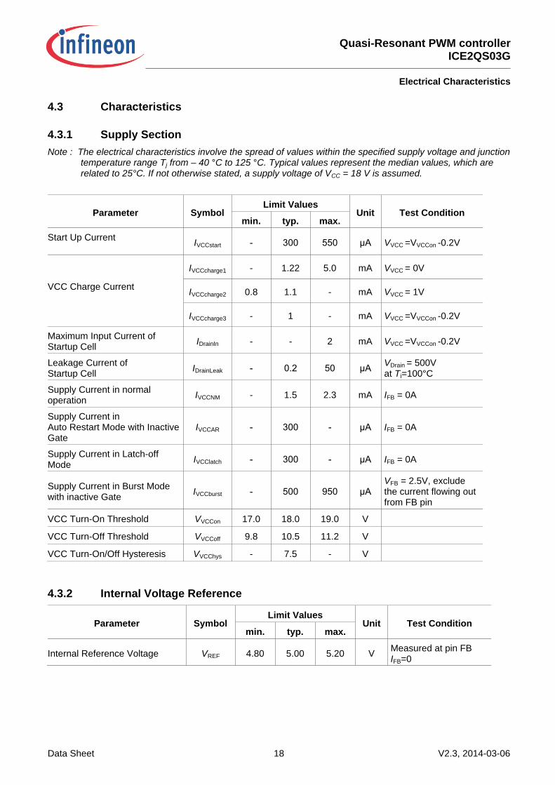
4.3 Characteristics
4.3.1 Supply Section
Note : The electrical characteristics involve the spread of values within the specified supply voltage and junctiontemperature range Tj from – 40 °C to 125 °C. Typical values represent the median values, which arerelated to 25°C. If not otherwise stated, a supply voltage of VCC = 18 V is assumed.
Parameter SymbolLimit Values
Unit Test Conditionmin. typ. max.
Start Up CurrentIVCCstart - 300 550 μA VVCC =VVCCon -0.2V
VCC Charge Current
IVCCcharge1 - 1.22 5.0 mA VVCC = 0V
IVCCcharge2 0.8 1.1 - mA VVCC = 1V
IVCCcharge3 - 1 - mA VVCC =VVCCon -0.2V
Maximum Input Current ofStartup Cell
IDrainIn - - 2 mA VVCC =VVCCon -0.2V
Leakage Current ofStartup Cell
IDrainLeak - 0.2 50 μA VDrain = 500Vat Tj=100°C
Supply Current in normaloperation
IVCCNM - 1.5 2.3 mA IFB = 0A
Supply Current inAuto Restart Mode with InactiveGate
IVCCAR - 300 - μA IFB = 0A
Supply Current in Latch-offMode
IVCClatch - 300 - μA IFB = 0A
Supply Current in Burst Modewith inactive Gate
IVCCburst - 500 950 μA VFB = 2.5V, excludethe current flowing outfrom FB pin
VCC Turn-On Threshold VVCCon 17.0 18.0 19.0 V
VCC Turn-Off Threshold VVCCoff 9.8 10.5 11.2 V
VCC Turn-On/Off Hysteresis VVCChys - 7.5 - V
4.3.2 Internal Voltage Reference
Parameter SymbolLimit Values
Unit Test Conditionmin. typ. max.
Internal Reference Voltage VREF 4.80 5.00 5.20 VMeasured at pin FBIFB=0
Quasi-Resonant PWM controllerICE2QS03G
Electrical Characteristics
Data Sheet 19 V2.3, 2014-03-06
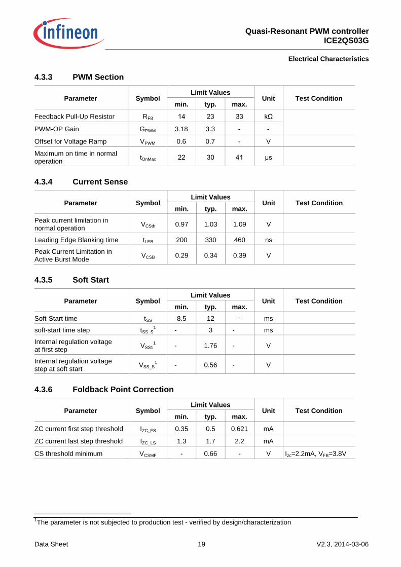
4.3.3 PWM Section
Parameter SymbolLimit Values
Unit Test Conditionmin. typ. max.
Feedback Pull-Up Resistor RFB 14 23 33 kΩ
PWM-OP Gain GPWM 3.18 3.3 - -
Offset for Voltage Ramp VPWM 0.6 0.7 - V
Maximum on time in normaloperation
tOnMax 22 30 41 μs
4.3.4 Current Sense
Parameter SymbolLimit Values
Unit Test Conditionmin. typ. max.
Peak current limitation innormal operation
VCSth 0.97 1.03 1.09 V
Leading Edge Blanking time tLEB 200 330 460 ns
Peak Current Limitation inActive Burst Mode
VCSB 0.29 0.34 0.39 V
4.3.5 Soft Start
Parameter SymbolLimit Values
Unit Test Conditionmin. typ. max.
Soft-Start time tSS 8.5 12 - ms
soft-start time step tSS_S1
- 3 - ms
Internal regulation voltageat first step
VSS11
- 1.76 - V
Internal regulation voltagestep at soft start
VSS_S1
- 0.56 - V
4.3.6 Foldback Point Correction
Parameter SymbolLimit Values
Unit Test Conditionmin. typ. max.
ZC current first step threshold IZC_FS 0.35 0.5 0.621 mA
ZC current last step threshold IZC_LS 1.3 1.7 2.2 mA
CS threshold minimum VCSMF - 0.66 - V Izc=2.2mA, VFB=3.8V
1The parameter is not subjected to production test - verified by design/characterization
Quasi-Resonant PWM controllerICE2QS03G
Electrical Characteristics
Data Sheet 20 V2.3, 2014-03-06
4.3.7 Digital Zero Crossing
Parameter SymbolLimit Values
Unit Test Conditionmin. typ. max.
Zero crossing thresholdvoltage
VZCCT 50 100 170 mV
Ringing suppression threshold VZCRS - 0.7 - V
Minimum ringing suppressiontime
tZCRS1 1.62 2.5 4.5 μs VZC > VZCRS
Maximum ringing suppressiontime
tZCRS2 - 25 - μs VZC < VZCRS
Threshold to set Up/DownCounter to one
VFBR1 - 3.9 - V
Threshold for downwardcounting at low line
VFBZHL - 3.2 - V
Threshold for upward countingat low line
VFBZLL - 2.5 - V
Threshold for downwardcounting at high line
VFBZHH - 2.9 - V
Threshold for upward countingat high line
VFBZLH - 2.3 - V
ZC current for IC switchthreshold to high line
IZCSH - 1.3 - mA
ZC current for IC switchthreshold to low line
IZCSL - 0.8 - mA
Counter time1
tCOUNT - 48 - ms
Maximum restart time innormal operation
tOffMax 30 42 57.5 μs
4.3.8 Active Burst Mode
Parameter SymbolLimit Values
Unit Test Conditionmin. typ. max.
Feedback voltage for enteringActive Burst Mode
VFBEB - 1.25 - V
Minimum Up/down value forentering Active Burst Mode
NZC_ABM - 7 -
Blanking time for enteringActive Burst Mode
tBEB - 24 - ms
Feedback voltage for leavingActive Burst Mode
VFBLB - 4.5 - V
Feedback voltage for burst-on VFBBOn - 3.6 - V
Feedback voltage for burst-off VFBBOff - 3.0 - V
1The parameter is not subjected to production test - verified by design/characterization
Quasi-Resonant PWM controllerICE2QS03G
Electrical Characteristics
Data Sheet 21 V2.3, 2014-03-06
Fixed Switching Frequency inActive Burst Mode
fsB 39 52 65 kHz
Max. Duty Cycle in ActiveBurst Mode
DmaxB - 0.5 -
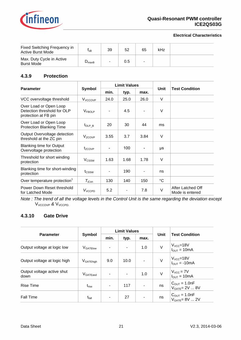
4.3.9 Protection
Parameter SymbolLimit Values
Unit Test Conditionmin. typ. max.
VCC overvoltage threshold VVCCOVP 24.0 25.0 26.0 V
Over Load or Open LoopDetection threshold for OLPprotection at FB pin
VFBOLP - 4.5 - V
Over Load or Open LoopProtection Blanking Time
tOLP_B 20 30 44 ms
Output Overvoltage detectionthreshold at the ZC pin
VZCOVP 3.55 3.7 3.84 V
Blanking time for OutputOvervoltage protection
tZCOVP - 100 - μs
Threshold for short windingprotection
VCSSW 1.63 1.68 1.78 V
Blanking time for short-windingprotection
tCSSW - 190 - ns
Over temperature protection1
TjCon 130 140 150 °C
Power Down Reset thresholdfor Latched Mode
VVCCPD 5.2 - 7.8 VAfter Latched OffMode is entered
Note : The trend of all the voltage levels in the Control Unit is the same regarding the deviation exceptVVCCOVP & VVCCPD.
4.3.10 Gate Drive
Parameter SymbolLimit Values
Unit Test Conditionmin. typ. max.
Output voltage at logic low VGATElow - - 1.0 VVVCC=18VIOUT = 10mA
Output voltage at logic high VGATEhigh 9.0 10.0 - VVVCC=18VIOUT = -10mA
Output voltage active shutdown
VGATEasd - - 1.0 VVVCC = 7VIOUT = 10mA
Rise Time trise - 117 - nsCOUT = 1.0nFVGATE= 2V ... 8V
Fall Time tfall - 27 - nsCOUT = 1.0nFVGATE= 8V ... 2V
Quasi-Resonant PWM controllerICE2QS03G
Outline Dimension
Data Sheet 22 V2.3, 2014-03-06
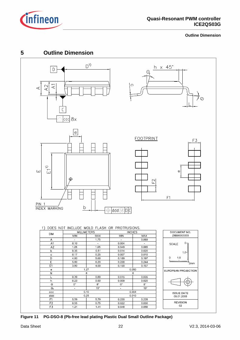
5 Outline Dimension
Figure 11 PG-DSO-8 (Pb-free lead plating Plastic Dual Small Outline Package)
Quasi-Resonant PWM controllerICE2QS03G
Marking
Data Sheet 23 V2.3, 2014-03-06
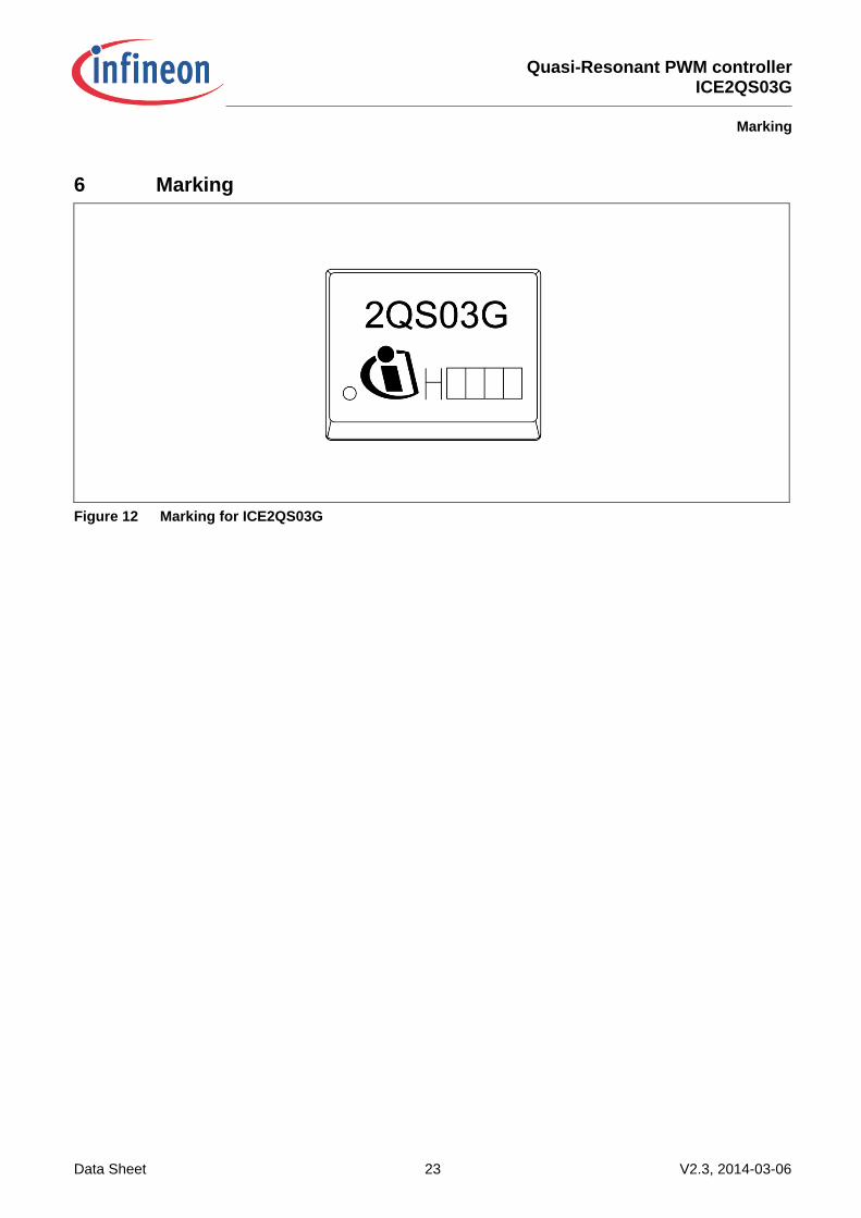
6 Marking
Figure 12 Marking for ICE2QS03G

w w w . i n f i n e o n . c o m
Published by Infineon Technologies AG