Embed Size (px)
Citation preview
Datasheet PleasereadtheImportantNoticeandWarningsattheendofthisdocument V2.1www.infineon.com 2017-06-30
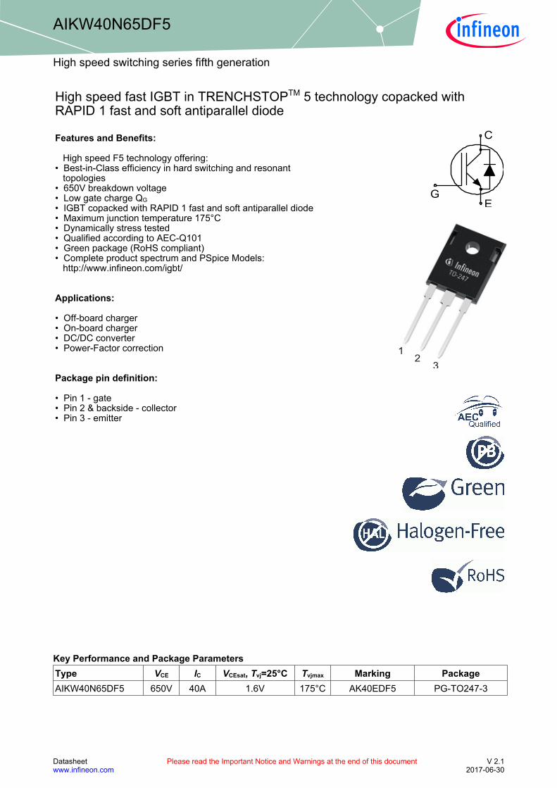
AIKW40N65DF5
Highspeedswitchingseriesfifthgeneration
HighspeedfastIGBTinTRENCHSTOPTM5technologycopackedwithRAPID1fastandsoftantiparalleldiodeFeaturesandBenefits:
HighspeedF5technologyoffering:•Best-in-Classefficiencyinhardswitchingandresonanttopologies•650Vbreakdownvoltage•LowgatechargeQG•IGBTcopackedwithRAPID1fastandsoftantiparalleldiode•Maximumjunctiontemperature175°C•Dynamicallystresstested•QualifiedaccordingtoAEC-Q101•Greenpackage(RoHScompliant)•CompleteproductspectrumandPSpiceModels:http://www.infineon.com/igbt/
Applications:
•Off-boardcharger•On-boardcharger•DC/DCconverter•Power-Factorcorrection
Packagepindefinition:
•Pin1-gate•Pin2&backside-collector•Pin3-emitter
G
C
E
12
3
KeyPerformanceandPackageParametersType VCE IC VCEsat,Tvj=25°C Tvjmax Marking PackageAIKW40N65DF5 650V 40A 1.6V 175°C AK40EDF5 PG-TO247-3
Datasheet 2 V2.12017-06-30
AIKW40N65DF5
Highspeedswitchingseriesfifthgeneration
TableofContents
Description . . . . . . . . . . . . . . . . . . . . . . . . . . . . . . . . . . . . . . . . . . . . . . . . . . . . . . . . . . . . . . . . . . . . . . . . 1
Table of Contents . . . . . . . . . . . . . . . . . . . . . . . . . . . . . . . . . . . . . . . . . . . . . . . . . . . . . . . . . . . . . . . . . . . 2
Maximum Ratings . . . . . . . . . . . . . . . . . . . . . . . . . . . . . . . . . . . . . . . . . . . . . . . . . . . . . . . . . . . . . . . . . . . 3
Thermal Resistance . . . . . . . . . . . . . . . . . . . . . . . . . . . . . . . . . . . . . . . . . . . . . . . . . . . . . . . . . . . . . . . . . 3
Electrical Characteristics . . . . . . . . . . . . . . . . . . . . . . . . . . . . . . . . . . . . . . . . . . . . . . . . . . . . . . . . . . . . . . 4
Electrical Characteristics Diagrams . . . . . . . . . . . . . . . . . . . . . . . . . . . . . . . . . . . . . . . . . . . . . . . . . . . . . 7
Package Drawing . . . . . . . . . . . . . . . . . . . . . . . . . . . . . . . . . . . . . . . . . . . . . . . . . . . . . . . . . . . . . . . . . . .13
Testing Conditions . . . . . . . . . . . . . . . . . . . . . . . . . . . . . . . . . . . . . . . . . . . . . . . . . . . . . . . . . . . . . . . . . .14
Revision History . . . . . . . . . . . . . . . . . . . . . . . . . . . . . . . . . . . . . . . . . . . . . . . . . . . . . . . . . . . . . . . . . . . .15
Disclaimer . . . . . . . . . . . . . . . . . . . . . . . . . . . . . . . . . . . . . . . . . . . . . . . . . . . . . . . . . . . . . . . . . . . . . . . . .16
Datasheet 3 V2.12017-06-30
AIKW40N65DF5
Highspeedswitchingseriesfifthgeneration
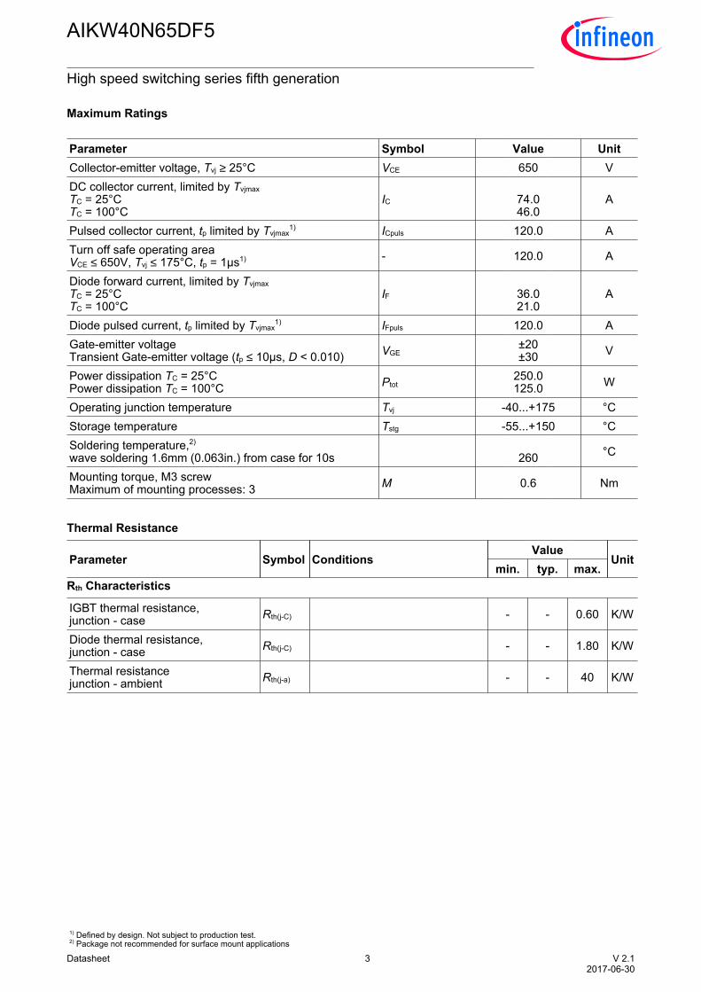
MaximumRatings
Parameter Symbol Value UnitCollector-emittervoltage,Tvj≥25°C VCE 650 V
DCcollectorcurrent,limitedbyTvjmaxTC=25°CTC=100°C
IC 74.046.0
A
Pulsedcollectorcurrent,tplimitedbyTvjmax1) ICpuls 120.0 A
Turn off safe operating areaVCE≤650V,Tvj≤175°C,tp=1µs1) - 120.0 A
Diodeforwardcurrent,limitedbyTvjmaxTC=25°CTC=100°C
IF 36.021.0
A
Diodepulsedcurrent,tplimitedbyTvjmax1) IFpuls 120.0 A
Gate-emitter voltageTransientGate-emittervoltage(tp≤10µs,D<0.010) VGE
±20±30 V
PowerdissipationTC=25°CPowerdissipationTC=100°C Ptot
250.0125.0 W
Operating junction temperature Tvj -40...+175 °C
Storage temperature Tstg -55...+150 °C
Soldering temperature,2)
wave soldering 1.6mm (0.063in.) from case for 10s 260 °C
Mounting torque, M3 screwMaximum of mounting processes: 3 M 0.6 Nm
ThermalResistance
Valuemin. typ. max.
Parameter Symbol Conditions Unit
RthCharacteristics
IGBT thermal resistance,junction - case Rth(j-C) - - 0.60 K/W
Diode thermal resistance,junction - case Rth(j-C) - - 1.80 K/W
Thermal resistancejunction - ambient Rth(j-a) - - 40 K/W
1) Defined by design. Not subject to production test.2) Package not recommended for surface mount applications
Datasheet 4 V2.12017-06-30
AIKW40N65DF5
Highspeedswitchingseriesfifthgeneration
ElectricalCharacteristic,atTvj=25°C,unlessotherwisespecified
Valuemin. typ. max.
Parameter Symbol Conditions Unit
StaticCharacteristic
Collector-emitter breakdown voltage V(BR)CES VGE=0V,IC=0.20mA 650 - - V
Collector-emitter saturation voltage VCEsat
VGE=15.0V,IC=40.0ATvj=25°CTvj=125°CTvj=175°C
---
1.601.801.90
2.10--
V
Diode forward voltage VF
VGE=0V,IF=20.0ATvj=25°CTvj=125°CTvj=175°C
---
1.551.531.49
1.80--
V
Gate-emitter threshold voltage VGE(th) IC=0.40mA,VCE=VGE 3.2 4.0 4.8 V
Zero gate voltage collector current ICESVCE=650V,VGE=0VTvj=25°CTvj=175°C
--
-1000
40-
µA
Gate-emitter leakage current IGES VCE=0V,VGE=20V - - 100 nA
Transconductance gfs VCE=20V,IC=40.0A - 50.0 - S
ElectricalCharacteristic,atTvj=25°C,unlessotherwisespecified
Valuemin. typ. max.
Parameter Symbol Conditions Unit
DynamicCharacteristic
Input capacitance Cies - 2500 -
Output capacitance Coes - 50 -
Reverse transfer capacitance Cres - 9 -
VCE=25V,VGE=0V,f=1MHz pF
Gate charge QGVCC=520V,IC=40.0A,VGE=15V - 95.0 - nC
Internal emitter inductancemeasured 5mm (0.197 in.) fromcase
LE - 13.0 - nH
SwitchingCharacteristic,InductiveLoad
Valuemin. typ. max.
Parameter Symbol Conditions Unit
IGBTCharacteristic,atTvj=25°CTurn-on delay time td(on) - 19 - ns
Rise time tr - 11 - ns
Turn-off delay time td(off) - 165 - ns
Fall time tf - 13 - ns
Turn-on energy Eon - 0.35 - mJ
Turn-off energy Eoff - 0.10 - mJ
Total switching energy Ets - 0.45 - mJ
Tvj=25°C,VCC=400V,IC=20.0A,VGE=0.0/15.0V,RG(on)=15.0Ω,RG(off)=15.0Ω,Lσ=30nH,Cσ=30pFLσ,CσfromFig.EEnergy losses include “tail” anddiode reverse recovery.
Datasheet 5 V2.12017-06-30
AIKW40N65DF5
Highspeedswitchingseriesfifthgeneration
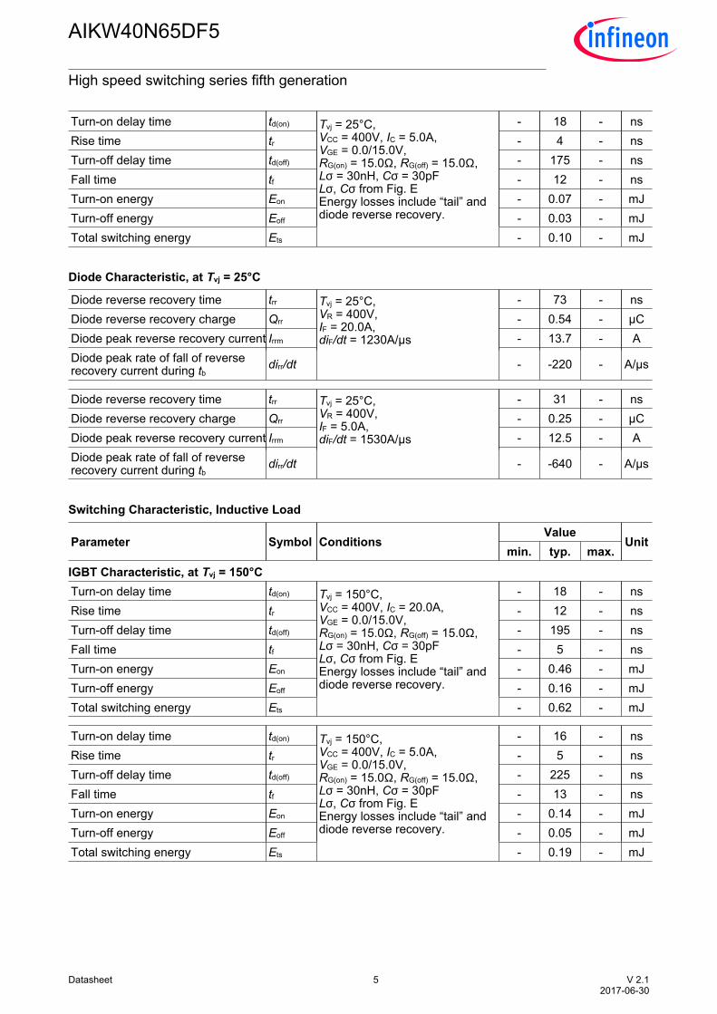
Turn-on delay time td(on) - 18 - ns
Rise time tr - 4 - ns
Turn-off delay time td(off) - 175 - ns
Fall time tf - 12 - ns
Turn-on energy Eon - 0.07 - mJ
Turn-off energy Eoff - 0.03 - mJ
Total switching energy Ets - 0.10 - mJ
Tvj=25°C,VCC=400V,IC=5.0A,VGE=0.0/15.0V,RG(on)=15.0Ω,RG(off)=15.0Ω,Lσ=30nH,Cσ=30pFLσ,CσfromFig.EEnergy losses include “tail” anddiode reverse recovery.
DiodeCharacteristic,atTvj=25°C
Diode reverse recovery time trr - 73 - ns
Diode reverse recovery charge Qrr - 0.54 - µC
Diode peak reverse recovery current Irrm - 13.7 - A
Diode peak rate of fall of reverserecoverycurrentduringtb dirr/dt - -220 - A/µs
Tvj=25°C,VR=400V,IF=20.0A,diF/dt=1230A/µs
Diode reverse recovery time trr - 31 - ns
Diode reverse recovery charge Qrr - 0.25 - µC
Diode peak reverse recovery current Irrm - 12.5 - A
Diode peak rate of fall of reverserecoverycurrentduringtb dirr/dt - -640 - A/µs
Tvj=25°C,VR=400V,IF=5.0A,diF/dt=1530A/µs
SwitchingCharacteristic,InductiveLoad
Valuemin. typ. max.
Parameter Symbol Conditions Unit
IGBTCharacteristic,atTvj=150°CTurn-on delay time td(on) - 18 - ns
Rise time tr - 12 - ns
Turn-off delay time td(off) - 195 - ns
Fall time tf - 5 - ns
Turn-on energy Eon - 0.46 - mJ
Turn-off energy Eoff - 0.16 - mJ
Total switching energy Ets - 0.62 - mJ
Tvj=150°C,VCC=400V,IC=20.0A,VGE=0.0/15.0V,RG(on)=15.0Ω,RG(off)=15.0Ω,Lσ=30nH,Cσ=30pFLσ,CσfromFig.EEnergy losses include “tail” anddiode reverse recovery.
Turn-on delay time td(on) - 16 - ns
Rise time tr - 5 - ns
Turn-off delay time td(off) - 225 - ns
Fall time tf - 13 - ns
Turn-on energy Eon - 0.14 - mJ
Turn-off energy Eoff - 0.05 - mJ
Total switching energy Ets - 0.19 - mJ
Tvj=150°C,VCC=400V,IC=5.0A,VGE=0.0/15.0V,RG(on)=15.0Ω,RG(off)=15.0Ω,Lσ=30nH,Cσ=30pFLσ,CσfromFig.EEnergy losses include “tail” anddiode reverse recovery.
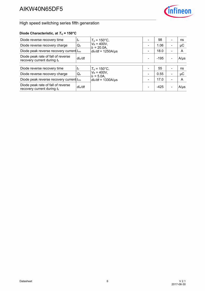
Datasheet 6 V2.12017-06-30
AIKW40N65DF5
Highspeedswitchingseriesfifthgeneration
DiodeCharacteristic,atTvj=150°C
Diode reverse recovery time trr - 98 - ns
Diode reverse recovery charge Qrr - 1.06 - µC
Diode peak reverse recovery current Irrm - 18.0 - A
Diode peak rate of fall of reverserecoverycurrentduringtb dirr/dt - -195 - A/µs
Tvj=150°C,VR=400V,IF=20.0A,diF/dt=1250A/µs
Diode reverse recovery time trr - 55 - ns
Diode reverse recovery charge Qrr - 0.55 - µC
Diode peak reverse recovery current Irrm - 17.0 - A
Diode peak rate of fall of reverserecoverycurrentduringtb dirr/dt - -425 - A/µs
Tvj=150°C,VR=400V,IF=5.0A,diF/dt=1330A/µs
Datasheet 7 V2.12017-06-30
AIKW40N65DF5
Highspeedswitchingseriesfifthgeneration
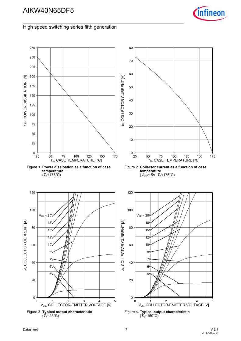
Figure 1. Powerdissipationasafunctionofcasetemperature(Tvj≤175°C)
TC,CASETEMPERATURE[°C]
Ptot ,PO
WER
DISSIPA
TION[W
]
25 50 75 100 125 150 1750
25
50
75
100
125
150
175
200
225
250
275
Figure 2. Collectorcurrentasafunctionofcasetemperature(VGE≥15V,Tvj≤175°C)
TC,CASETEMPERATURE[°C]
IC,C
OLLEC
TORCURREN
T[A]
25 50 75 100 125 150 1750
10
20
30
40
50
60
70
80
Figure 3. Typicaloutputcharacteristic(Tvj=25°C)
VCE,COLLECTOR-EMITTERVOLTAGE[V]
IC,C
OLLEC
TORCURREN
T[A]
0 1 2 3 4 50
20
40
60
80
100
120
VGE = 20V
18V
15V
12V
10V
8V
7V
6V
5V
Figure 4. Typicaloutputcharacteristic(Tvj=150°C)
VCE,COLLECTOR-EMITTERVOLTAGE[V]
IC,C
OLLEC
TORCURREN
T[A]
0 1 2 3 4 50
20
40
60
80
100
120
VGE = 20V
18V
15V
12V
10V
8V
7V
6V
5V
Datasheet 8 V2.12017-06-30
AIKW40N65DF5
Highspeedswitchingseriesfifthgeneration
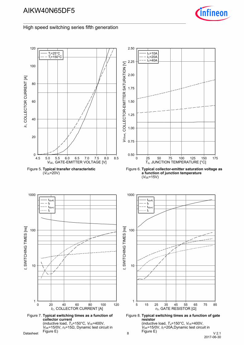
Figure 5. Typicaltransfercharacteristic(VCE=20V)
VGE,GATE-EMITTERVOLTAGE[V]
IC,C
OLLEC
TORCURREN
T[A]
4.5 5.0 5.5 6.0 6.5 7.0 7.5 8.0 8.50
20
40
60
80
100
120Tj=25°CTj=150°C
Figure 6. Typicalcollector-emittersaturationvoltageasafunctionofjunctiontemperature(VGE=15V)
Tvj,JUNCTIONTEMPERATURE[°C]
VCEsat,C
OLLEC
TOR-EMITTE
RSAT
URAT
ION[V
]
0 25 50 75 100 125 150 1750.50
0.75
1.00
1.25
1.50
1.75
2.00
2.25
2.50IC=10AIC=20AIC=40A
Figure 7. Typicalswitchingtimesasafunctionofcollectorcurrent(inductiveload,Tvj=150°C,VCE=400V,VGE=15/0V,rG=15Ω,DynamictestcircuitinFigure E)
IC,COLLECTORCURRENT[A]
t,SW
ITCHINGTIMES
[ns]
0 20 40 60 80 100 1201
10
100
1000td(off)
tftd(on)
tr
Figure 8. Typicalswitchingtimesasafunctionofgateresistor(inductiveload,Tvj=150°C,VCE=400V,VGE=15/0V,IC=20A,DynamictestcircuitinFigure E)
rG,GATERESISTOR[Ω]
t,SW
ITCHINGTIMES
[ns]
5 15 25 35 45 55 65 75 851
10
100
1000td(off)
tftd(on)
tr
Datasheet 9 V2.12017-06-30
AIKW40N65DF5
Highspeedswitchingseriesfifthgeneration
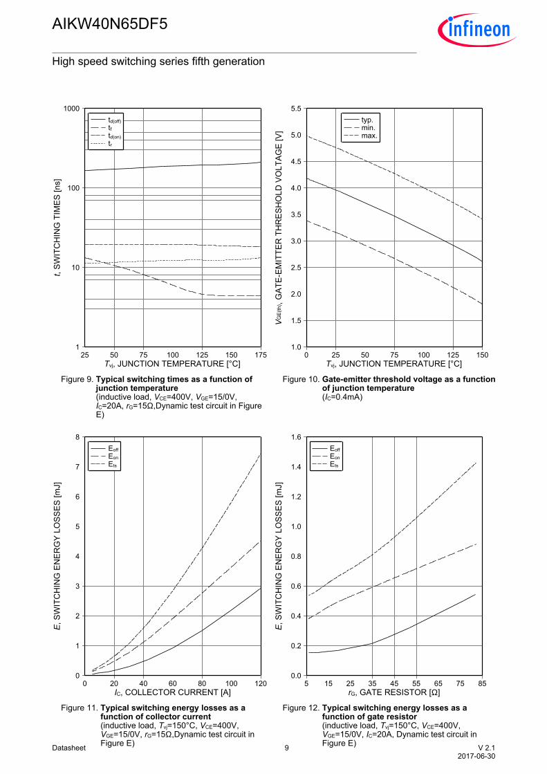
Figure 9. Typicalswitchingtimesasafunctionofjunctiontemperature(inductiveload,VCE=400V,VGE=15/0V,IC=20A,rG=15Ω,DynamictestcircuitinFigureE)
Tvj,JUNCTIONTEMPERATURE[°C]
t,SW
ITCHINGTIMES
[ns]
25 50 75 100 125 150 1751
10
100
1000td(off)
tftd(on)
tr
Figure 10. Gate-emitterthresholdvoltageasafunctionofjunctiontemperature(IC=0.4mA)
Tvj,JUNCTIONTEMPERATURE[°C]
VGE(th) ,GAT
E-EM
ITTE
RTHRES
HOLD
VOLTAG
E[V]
0 25 50 75 100 125 1501.0
1.5
2.0
2.5
3.0
3.5
4.0
4.5
5.0
5.5typ.min.max.
Figure 11. Typicalswitchingenergylossesasafunctionofcollectorcurrent(inductiveload,Tvj=150°C,VCE=400V,VGE=15/0V,rG=15Ω,DynamictestcircuitinFigure E)
IC,COLLECTORCURRENT[A]
E,S
WITCHINGENER
GYLO
SSES
[mJ]
0 20 40 60 80 100 1200
1
2
3
4
5
6
7
8Eoff
Eon
Ets
Figure 12. Typicalswitchingenergylossesasafunctionofgateresistor(inductiveload,Tvj=150°C,VCE=400V,VGE=15/0V,IC=20A,DynamictestcircuitinFigure E)
rG,GATERESISTOR[Ω]
E,S
WITCHINGENER
GYLO
SSES
[mJ]
5 15 25 35 45 55 65 75 850.0
0.2
0.4
0.6
0.8
1.0
1.2
1.4
1.6Eoff
Eon
Ets
Datasheet 10 V2.12017-06-30
AIKW40N65DF5
Highspeedswitchingseriesfifthgeneration
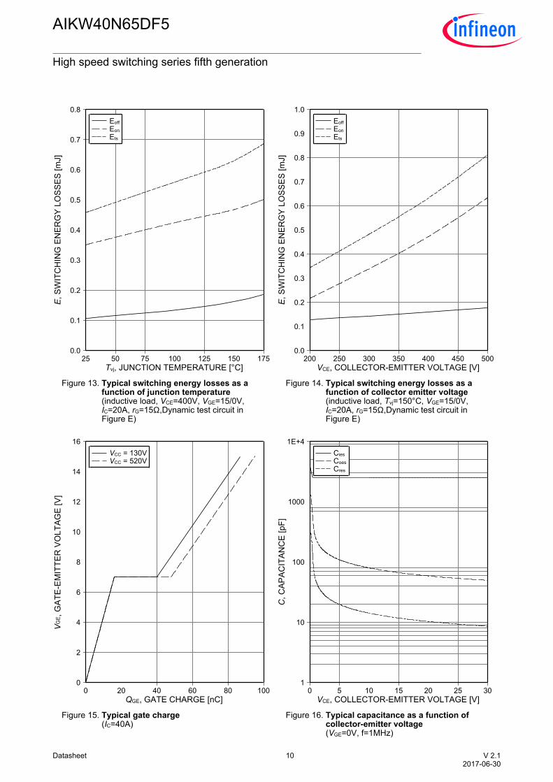
Figure 13. Typicalswitchingenergylossesasafunctionofjunctiontemperature(inductiveload,VCE=400V,VGE=15/0V,IC=20A,rG=15Ω,DynamictestcircuitinFigure E)
Tvj,JUNCTIONTEMPERATURE[°C]
E,S
WITCHINGENER
GYLO
SSES
[mJ]
25 50 75 100 125 150 1750.0
0.1
0.2
0.3
0.4
0.5
0.6
0.7
0.8Eoff
Eon
Ets
Figure 14. Typicalswitchingenergylossesasafunctionofcollectoremittervoltage(inductiveload,Tvj=150°C,VGE=15/0V,IC=20A,rG=15Ω,DynamictestcircuitinFigure E)
VCE,COLLECTOR-EMITTERVOLTAGE[V]
E,S
WITCHINGENER
GYLO
SSES
[mJ]
200 250 300 350 400 450 5000.0
0.1
0.2
0.3
0.4
0.5
0.6
0.7
0.8
0.9
1.0Eoff
Eon
Ets
Figure 15. Typicalgatecharge(IC=40A)
QGE,GATECHARGE[nC]
VGE ,GAT
E-EM
ITTE
RVOLTAG
E[V]
0 20 40 60 80 1000
2
4
6
8
10
12
14
16VCC=130VVCC=520V
Figure 16. Typicalcapacitanceasafunctionofcollector-emittervoltage(VGE=0V,f=1MHz)
VCE,COLLECTOR-EMITTERVOLTAGE[V]
C,C
APAC
ITAN
CE[pF]
0 5 10 15 20 25 301
10
100
1000
1E+4Cies
Coes
Cres
Datasheet 11 V2.12017-06-30
AIKW40N65DF5
Highspeedswitchingseriesfifthgeneration
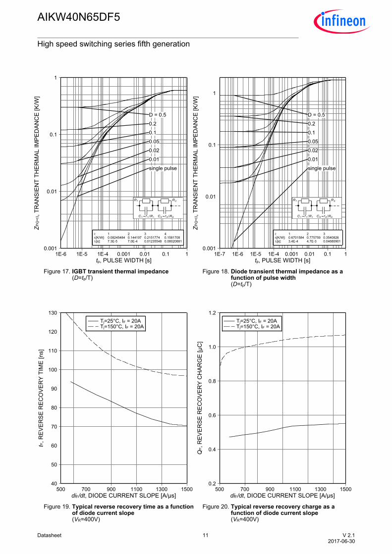
Figure 17. IGBTtransientthermalimpedance(D=tp/T)
tp,PULSEWIDTH[s]
Zth(j -c
) ,TR
ANSIEN
TTH
ERMAL
IMPE
DAN
CE[K/W
]
1E-6 1E-5 1E-4 0.001 0.01 0.1 10.001
0.01
0.1
1
D = 0.5
0.2
0.1
0.05
0.02
0.01
single pulse
i:ri[K/W]:τi[s]:
10.082454847.3E-5
20.1441977.0E-4
30.21517740.01235548
40.15817080.08020881
Figure 18. Diodetransientthermalimpedanceasafunctionofpulsewidth(D=tp/T)
tp,PULSEWIDTH[s]
Zth(j -c
) ,TR
ANSIEN
TTH
ERMAL
IMPE
DAN
CE[K/W
]
1E-7 1E-6 1E-5 1E-4 0.001 0.01 0.1 10.001
0.01
0.1
1
D = 0.5
0.2
0.1
0.05
0.02
0.01
single pulse
i:ri[K/W]:τi[s]:
10.67015843.4E-4
20.7757594.7E-3
30.35408260.04680901
Figure 19. Typicalreverserecoverytimeasafunctionofdiodecurrentslope(VR=400V)
diF/dt,DIODECURRENTSLOPE[A/µs]
trr,R
EVER
SEREC
OVE
RYTIME[ns]
500 700 900 1100 1300 150040
50
60
70
80
90
100
110
120
130Tj=25°C, IF = 20ATj=150°C, IF = 20A
Figure 20. Typicalreverserecoverychargeasafunctionofdiodecurrentslope(VR=400V)
diF/dt,DIODECURRENTSLOPE[A/µs]
Qrr ,REV
ERSE
REC
OVE
RYCHAR
GE[µC]
500 700 900 1100 1300 15000.2
0.4
0.6
0.8
1.0
1.2Tj=25°C, IF = 20ATj=150°C, IF = 20A
Datasheet 12 V2.12017-06-30
AIKW40N65DF5
Highspeedswitchingseriesfifthgeneration
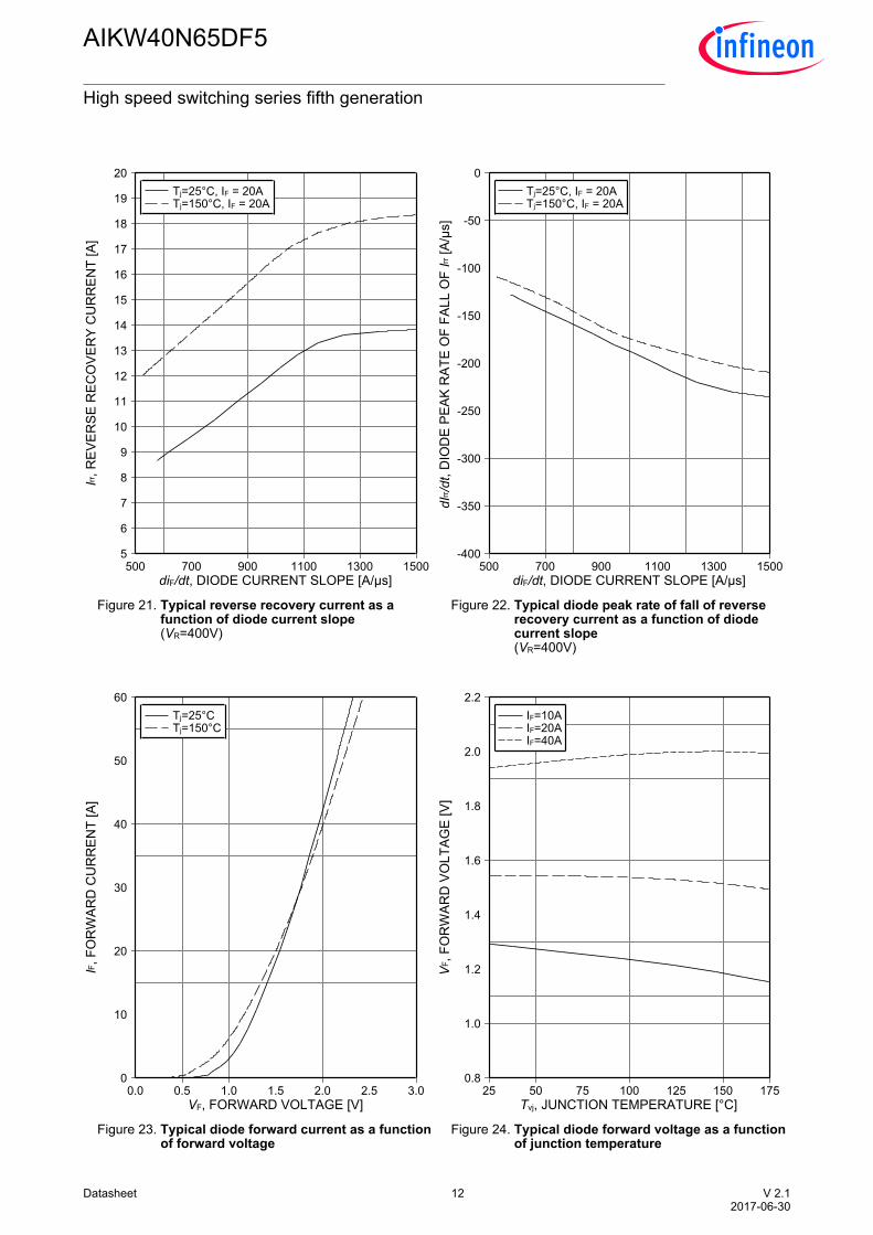
Figure 21. Typicalreverserecoverycurrentasafunctionofdiodecurrentslope(VR=400V)
diF/dt,DIODECURRENTSLOPE[A/µs]
Irr,R
EVER
SEREC
OVE
RYCURREN
T[A]
500 700 900 1100 1300 15005
6
7
8
9
10
11
12
13
14
15
16
17
18
19
20Tj=25°C, IF = 20ATj=150°C, IF = 20A
Figure 22. Typicaldiodepeakrateoffallofreverserecoverycurrentasafunctionofdiodecurrentslope(VR=400V)
diF/dt,DIODECURRENTSLOPE[A/µs]
dIrr /dt,D
IODEPE
AKRAT
EOFFA
LLOFIrr[A
/µs]
500 700 900 1100 1300 1500-400
-350
-300
-250
-200
-150
-100
-50
0Tj=25°C, IF = 20ATj=150°C, IF = 20A
Figure 23. Typicaldiodeforwardcurrentasafunctionofforwardvoltage
VF,FORWARDVOLTAGE[V]
IF ,FORWAR
DCURREN
T[A]
0.0 0.5 1.0 1.5 2.0 2.5 3.00
10
20
30
40
50
60Tj=25°CTj=150°C
Figure 24. Typicaldiodeforwardvoltageasafunctionofjunctiontemperature
Tvj,JUNCTIONTEMPERATURE[°C]
VF ,FO
RWAR
DVOLTAG
E[V]
25 50 75 100 125 150 1750.8
1.0
1.2
1.4
1.6
1.8
2.0
2.2IF=10AIF=20AIF=40A
Datasheet 13 V2.12017-06-30
AIKW40N65DF5
Highspeedswitchingseriesfifthgeneration
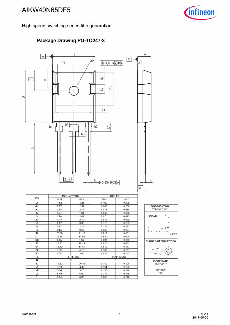
Package Drawing PG-TO247-3
Datasheet 14 V2.12017-06-30
AIKW40N65DF5
Highspeedswitchingseriesfifthgeneration
t
a b
td(off)
tf t
rtd(on)
90% IC
10% IC
90% IC
10% VGE
10% IC
t
90% VGE
t
t
90% VGE
VGE
(t)
t
t
tt1 t
4
2% IC
10% VGE
2% VCE
t2
t3
E
t
t
V I toff
= x x d
1
2
CE CE
t
t
V I ton
= x x d
3
4
CE C
CC
dI /dtF
dI
I,V
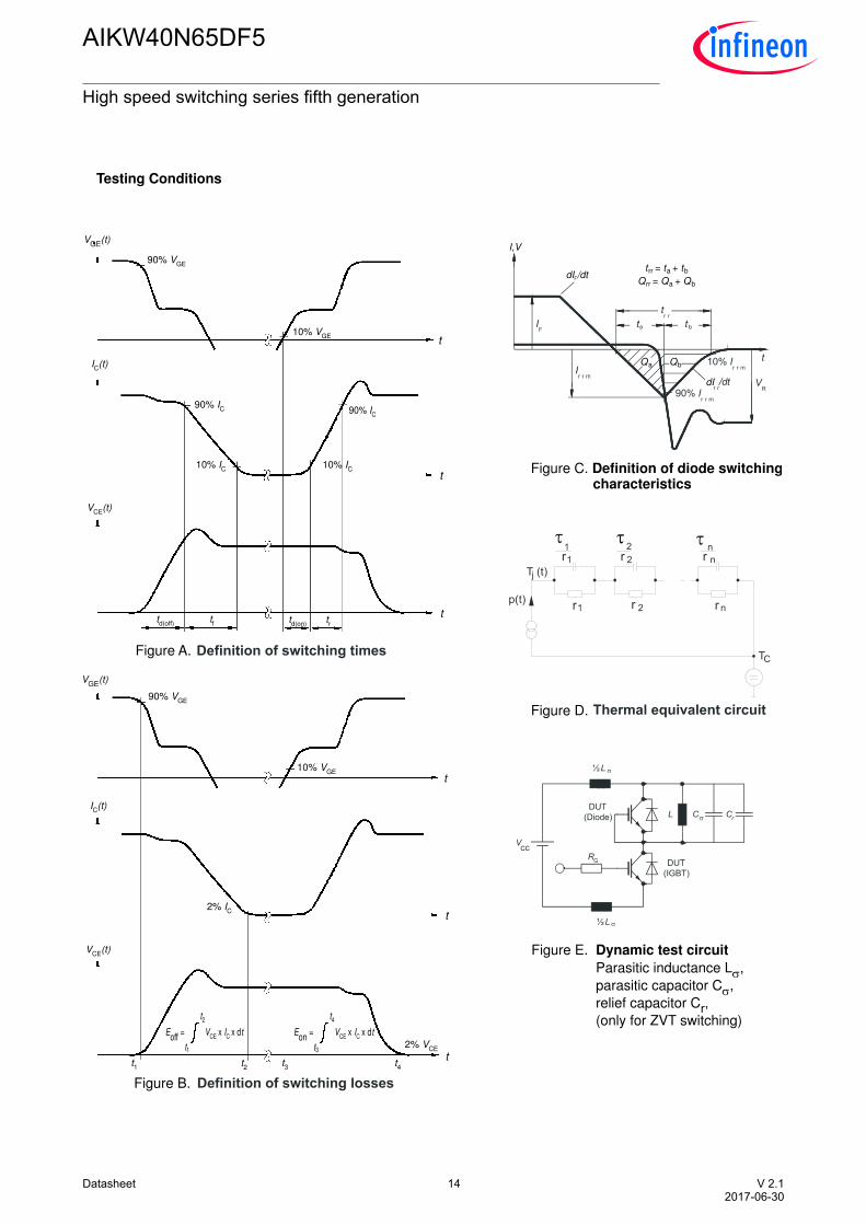
Figure A.
Figure B.
Figure C. Definition of diode switchingcharacteristics
Figure E. Dynamic test circuit
Figure D.
I (t)C
Parasitic inductance L ,
parasitic capacitor C ,
relief capacitor C ,
(only for ZVT switching)
s
s
r
t t t
Q Q Qrr a b
rr a b
= +
= +
Qa Qb
V (t)CE
VGE
(t)
I (t)C
V (t)CE
Testing Conditions
Datasheet 15 V2.12017-06-30
AIKW40N65DF5
Highspeedswitchingseriesfifthgeneration
RevisionHistory
AIKW40N65DF5
Revision:2017-06-30,Rev.2.1Previous Revision
Revision Date Subjects (major changes since last revision)
2.1 2017-06-30 Data sheet created

TrademarksofInfineonTechnologiesAGµHVIC™,µIPM™,µPFC™,AU-ConvertIR™,AURIX™,C166™,CanPAK™,CIPOS™,CIPURSE™,CoolDP™,CoolGaN™,COOLiR™,CoolMOS™,CoolSET™,CoolSiC™,DAVE™,DI-POL™,DirectFET™,DrBlade™,EasyPIM™,EconoBRIDGE™,EconoDUAL™,EconoPACK™,EconoPIM™,EiceDRIVER™,eupec™,FCOS™,GaNpowIR™,HEXFET™,HITFET™,HybridPACK™,iMOTION™,IRAM™,ISOFACE™,IsoPACK™,LEDrivIR™,LITIX™,MIPAQ™,ModSTACK™,my-d™,NovalithIC™,OPTIGA™,OptiMOS™,ORIGA™,PowIRaudio™,PowIRStage™,PrimePACK™,PrimeSTACK™,PROFET™,PRO-SIL™,RASIC™,REAL3™,SmartLEWIS™,SOLIDFLASH™,SPOC™,StrongIRFET™,SupIRBuck™,TEMPFET™,TRENCHSTOP™,TriCore™,UHVIC™,XHP™,XMC™TrademarksupdatedNovember2015OtherTrademarksAllreferencedproductorservicenamesandtrademarksarethepropertyoftheirrespectiveowners.
PublishedbyInfineonTechnologiesAG81726München,Germany©InfineonTechnologiesAG2017.AllRightsReserved.
ImportantNoticeTheinformationgiveninthisdocumentshallinnoeventberegardedasaguaranteeofconditionsorcharacteristics(“Beschaffenheitsgarantie”).Withrespecttoanyexamples,hintsoranytypicalvaluesstatedhereinand/oranyinformationregardingtheapplicationoftheproduct,InfineonTechnologiesherebydisclaimsanyandallwarrantiesandliabilitiesofanykind,includingwithoutlimitationwarrantiesofnon-infringementofintellectualpropertyrightsofanythirdparty.
Inaddition,anyinformationgiveninthisdocumentissubjecttocustomer’scompliancewithitsobligationsstatedinthisdocumentandanyapplicablelegalrequirements,normsandstandardsconcerningcustomer’sproductsandanyuseoftheproductofInfineonTechnologiesincustomer’sapplications.
Thedatacontainedinthisdocumentisexclusivelyintendedfortechnicallytrainedstaff.Itistheresponsibilityofcustomer’stechnicaldepartmentstoevaluatethesuitabilityoftheproductfortheintendedapplicationandthecompletenessoftheproductinformationgiveninthisdocumentwithrespecttosuchapplication.
Forfurtherinformationontheproduct,technology,deliverytermsandconditionsandpricespleasecontactyournearestInfineonTechnologiesoffice(www.infineon.com).
WarningsDuetotechnicalrequirementsproductsmaycontaindangeroussubstances.ForinformationonthetypesinquestionpleasecontactyournearestInfineonTechnologiesoffice.
ExceptasotherwiseexplicitlyapprovedbyInfineonTechnologiesinawrittendocumentsignedbyauthorizedrepresentativesofInfineonTechnologies,InfineonTechnologies’productsmaynotbeusedinanyapplicationswhereafailureoftheproductoranyconsequencesoftheusethereofcanreasonablybeexpectedtoresultinpersonalinjury.