Embed Size (px)
Citation preview
Industr ia l Power Control
Diode Silicon Carbide Schottky Diode
Final Data Sheet Rev. 2.1, 2021-06-09
IDM02G120C5 5th Generation CoolSiC™ 1200 V SiC Schottky Diode
1) J-STD20 and JESD22
Final Data Sheet 2 Rev.2.1, 2021-06-09
5th Generation CoolSiC™ 1200 V SiC Schottky Diode
IDM02G120C5
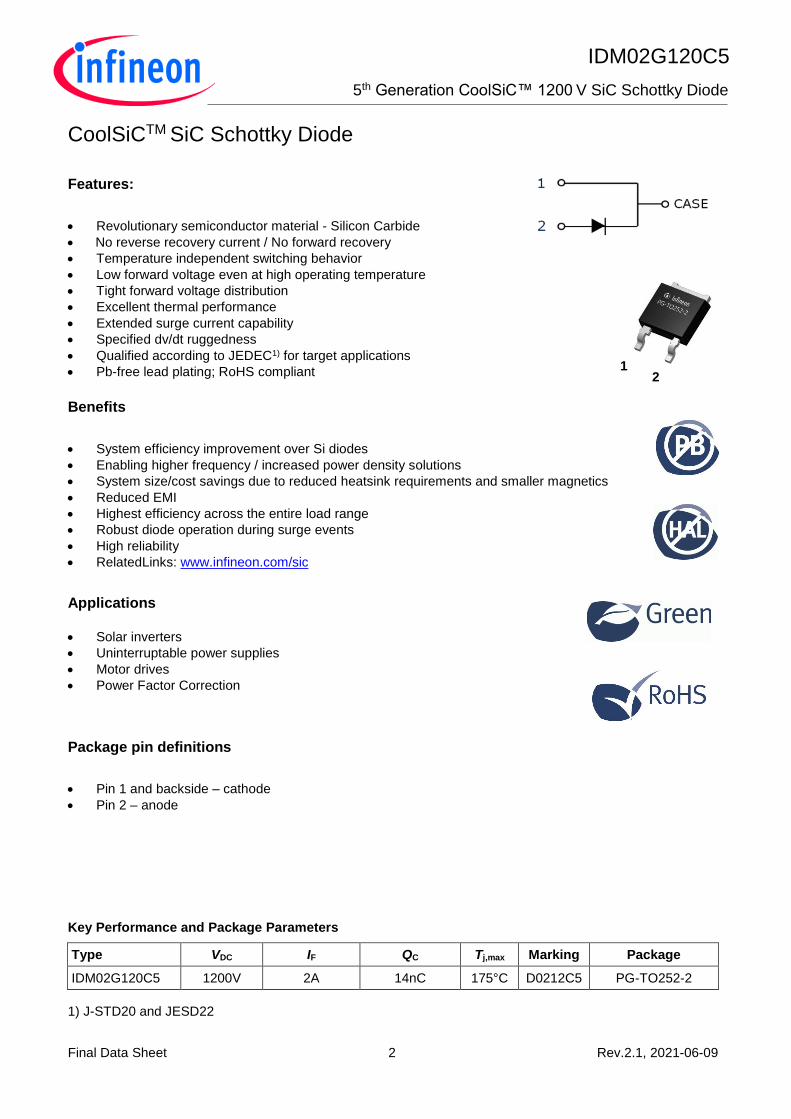
CoolSiCTM SiC Schottky Diode
Features:
Revolutionary semiconductor material - Silicon Carbide
No reverse recovery current / No forward recovery
Temperature independent switching behavior
Low forward voltage even at high operating temperature
Tight forward voltage distribution
Excellent thermal performance
Extended surge current capability
Specified dv/dt ruggedness
Qualified according to JEDEC1) for target applications
Pb-free lead plating; RoHS compliant
Benefits
System efficiency improvement over Si diodes
Enabling higher frequency / increased power density solutions
System size/cost savings due to reduced heatsink requirements and smaller magnetics
Reduced EMI
Highest efficiency across the entire load range
Robust diode operation during surge events
High reliability
RelatedLinks: www.infineon.com/sic
Applications
Solar inverters
Uninterruptable power supplies
Motor drives
Power Factor Correction
Package pin definitions
Pin 1 and backside – cathode
Pin 2 – anode Key Performance and Package Parameters
Type VDC IF QC Tj,max Marking Package
IDM02G120C5 1200V 2A 14nC 175°C D0212C5 PG-TO252-2
1 2
Final Data Sheet 3 Rev.2.1, 2021-06-09
5th Generation CoolSiC™ 1200 V SiC Schottky Diode
IDM02G120C5
Table of Contents
Description…. ............................................................................................................................................. 2
Table of Contents ........................................................................................................................................ 3
Maximum ratings ......................................................................................................................................... 4
Thermal Resistances .................................................................................................................................. 4
Electrical Characteristics ............................................................................................................................. 5
Electrical Characteristics diagram .............................................................................................................. 5
Package Drawings ...................................................................................................................................... 9
Revision History ........................................................................................................................................ 10
Disclaimer…. ............................................................................................................................................. 10
Final Data Sheet 4 Rev.2.1, 2021-06-09
5th Generation CoolSiC™ 1200 V SiC Schottky Diode
IDM02G120C5
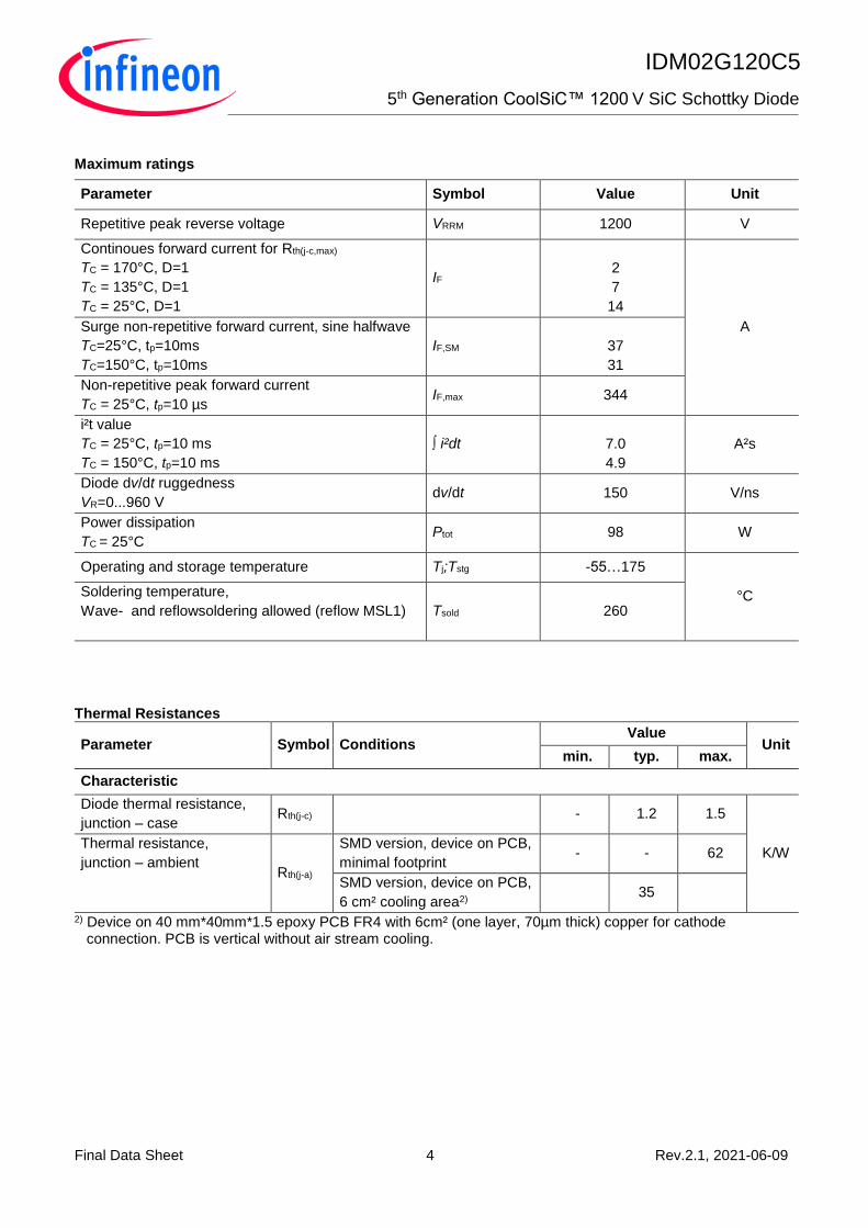
Maximum ratings
Parameter Symbol Value Unit
Repetitive peak reverse voltage VRRM 1200 V
Continoues forward current for Rth(j-c,max)
TC = 170°C, D=1
TC = 135°C, D=1
TC = 25°C, D=1
IF
2
7
14
A Surge non-repetitive forward current, sine halfwave
TC=25°C, tp=10ms
TC=150°C, tp=10ms
IF,SM
37
31
Non-repetitive peak forward current
TC = 25°C, tp=10 µs IF,max 344
i²t value
TC = 25°C, tp=10 ms
TC = 150°C, tp=10 ms
∫ i²dt
7.0
4.9
A²s
Diode dv/dt ruggedness
VR=0...960 V dv/dt 150 V/ns
Power dissipation
TC = 25°C Ptot 98 W
Operating and storage temperature Tj;Tstg -55…175
°C Soldering temperature,
Wave- and reflowsoldering allowed (reflow MSL1)
Tsold 260
Thermal Resistances
Parameter Symbol Conditions Value
Unit min. typ. max.
Characteristic
Diode thermal resistance,
junction – case Rth(j-c)
- 1.2 1.5
K/W Thermal resistance,
junction – ambient Rth(j-a)
SMD version, device on PCB,
minimal footprint - - 62
SMD version, device on PCB,
6 cm² cooling area2) 35
2) Device on 40 mm*40mm*1.5 epoxy PCB FR4 with 6cm² (one layer, 70µm thick) copper for cathode connection. PCB is vertical without air stream cooling.
Final Data Sheet 5 Rev.2.1, 2021-06-09
5th Generation CoolSiC™ 1200 V SiC Schottky Diode
IDM02G120C5
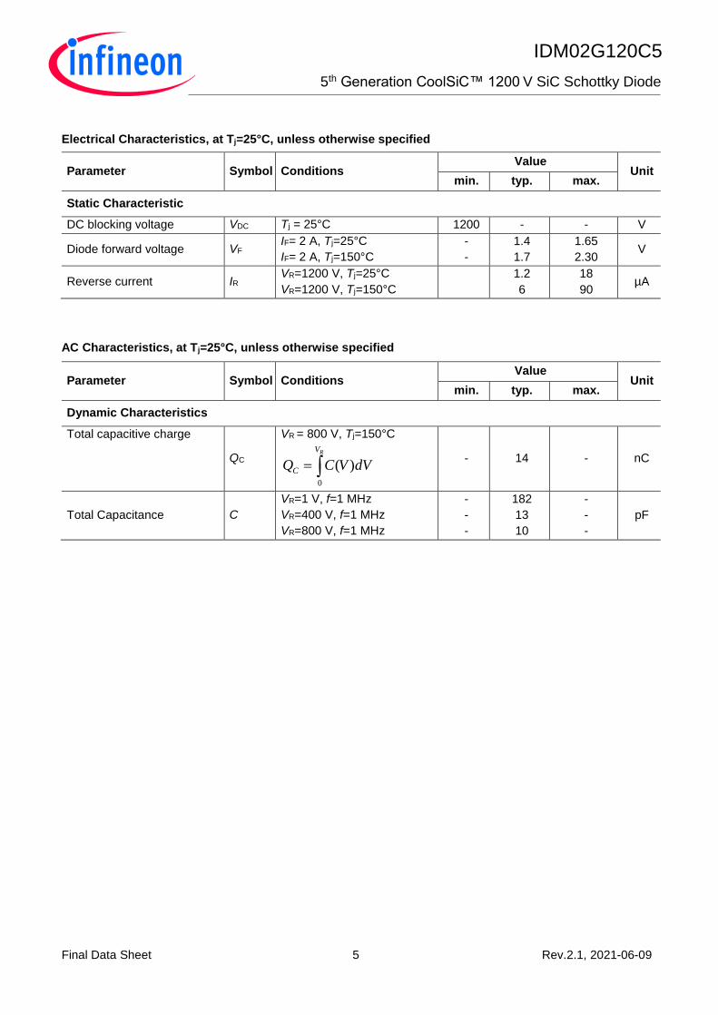
Electrical Characteristics, at Tj=25°C, unless otherwise specified
Parameter Symbol Conditions Value
Unit min. typ. max.
Static Characteristic
DC blocking voltage VDC Tj = 25°C 1200 - - V
Diode forward voltage VF IF= 2 A, Tj=25°C
IF= 2 A, Tj=150°C
-
-
1.4
1.7
1.65
2.30 V
Reverse current IR VR=1200 V, Tj=25°C
VR=1200 V, Tj=150°C
1.2
6
18
90 µA
AC Characteristics, at Tj=25°C, unless otherwise specified
Parameter Symbol Conditions Value
Unit min. typ. max.
Dynamic Characteristics
Total capacitive charge
QC
VR = 800 V, Tj=150°C
RV
C dVVCQ0
)( - 14 - nC
Total Capacitance C
VR=1 V, f=1 MHz
VR=400 V, f=1 MHz
VR=800 V, f=1 MHz
-
-
-
182
13
10
-
-
-
pF
Electrical Characteristics diagram
Final Data Sheet 6 Rev.2.1, 2021-06-09
5th Generation CoolSiC™ 1200 V SiC Schottky Diode
IDM02G120C5
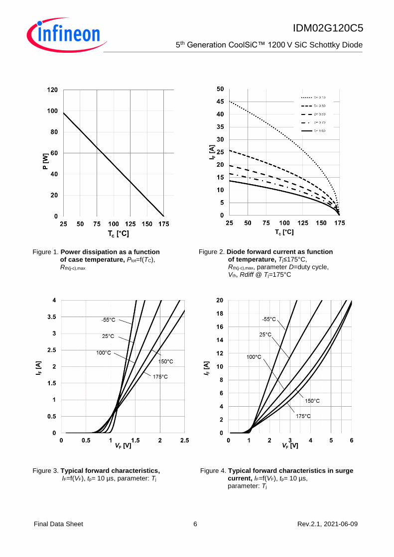
Figure 1. Power dissipation as a function of case temperature, Ptot=f(TC), Rth(j-c),max
Figure 2. Diode forward current as function of temperature, Tj≤175°C, Rth(j-c),max, parameter D=duty cycle, Vth, Rdiff @ Tj=175°C
Figure 3. Typical forward characteristics, IF=f(VF), tp= 10 µs, parameter: Tj
Figure 4. Typical forward characteristics in surge current, IF=f(VF), tp= 10 µs, parameter: Tj
Final Data Sheet 7 Rev.2.1, 2021-06-09
5th Generation CoolSiC™ 1200 V SiC Schottky Diode
IDM02G120C5
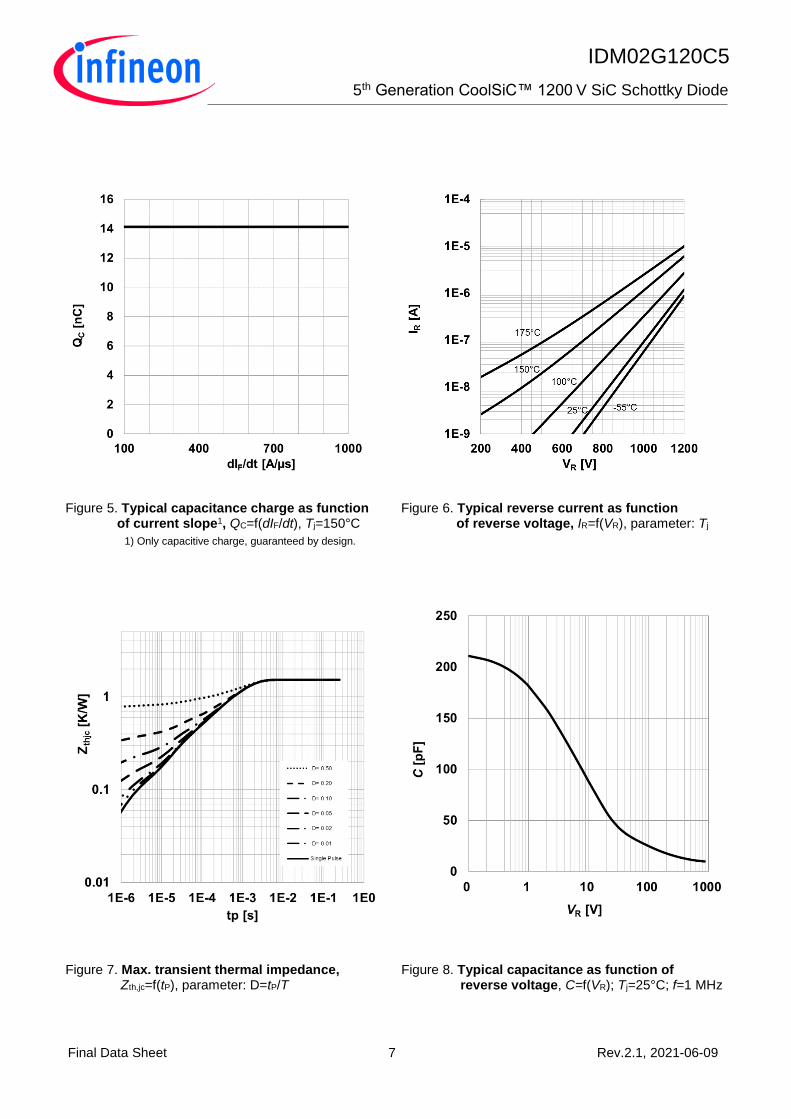
Figure 5. Typical capacitance charge as function of current slope1, QC=f(dIF/dt), Tj=150°C
1) Only capacitive charge, guaranteed by design.
Figure 6. Typical reverse current as function of reverse voltage, IR=f(VR), parameter: Tj
Figure 7. Max. transient thermal impedance, Zth,jc=f(tP), parameter: D=tP/T
Figure 8. Typical capacitance as function of reverse voltage, C=f(VR); Tj=25°C; f=1 MHz
Final Data Sheet 8 Rev.2.1, 2021-06-09
5th Generation CoolSiC™ 1200 V SiC Schottky Diode
IDM02G120C5
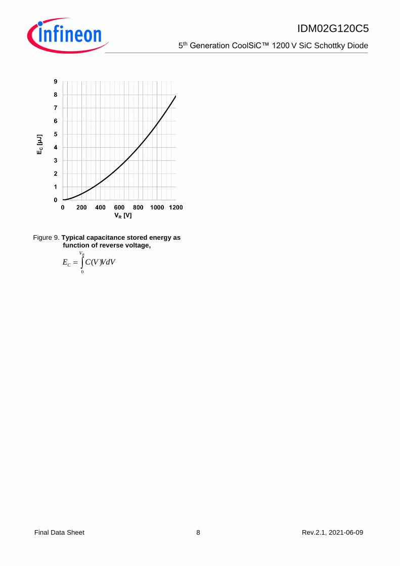
Figure 9. Typical capacitance stored energy as function of reverse voltage,
RV
C VdVVCE0
)(
Final Data Sheet 9 Rev.2.1, 2021-06-09
5th Generation CoolSiC™ 1200 V SiC Schottky Diode
IDM02G120C5
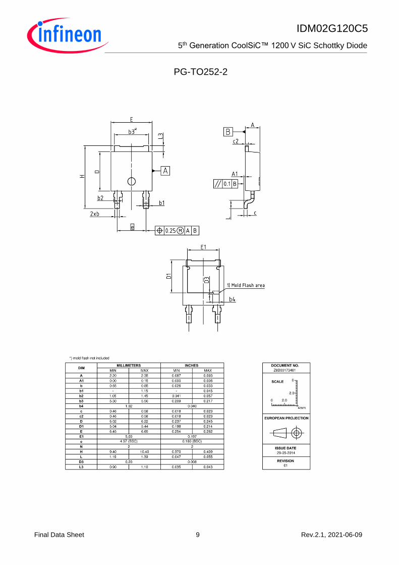
PG-TO252-2
Package Drawings
Final Data Sheet 10 Rev.2.1, 2021-06-09
5th Generation CoolSiC™ 1200 V SiC Schottky Diode
IDM02G120C5
Revision History
Disclaimer
We Listen to Your Comments Any information within this document that you feel is wrong, unclear or missing at all? Your feedback will help us to continuously improve the quality of this document. Please send your proposal (including a reference to this document) to: [email protected]
IIDM02G120C5
Revision: 2021-06-09, Rev. 2.1
Previous Revision:
Revision Date Subjects (major changes since last version)
2.0 2015-06-22 Final data sheet
2.1 2021-06-09 Increased dv/dt ruggedness
Final Data Sheet 11 Rev.2.1, 2021-06-09
5th Generation CoolSiC™ 1200 V SiC Schottky Diode
IDM02G120C5
Published by
Infineon Technologies AG
81726 München, Germany
© Infineon Technologies AG 2021.
All Rights Reserved.
Important Notice
The information given in this document shall in no event be regarded as a guarantee of conditions or characteristics (“Beschaffenheitsgarantie”). With respect to any examples, hints or any typical values stated herein and/or any information regarding the application of the product, Infineon Technologies hereby disclaims any and all warranties and liabilities of any kind, including without limitation warranties of non-infringement of intellectual property rights of any third party.
In addition, any information given in this document is subject to customer’s compliance with its obligations stated in this document and any applicable legal requirements, norms and standards concerning customer’s products and any use of the product of Infineon Technologies in customer’s applications.
The data contained in this document is exclusively intended for technically trained staff. It is the responsibility of customer’s technical departments to evaluate the suitability of the product for the intended application and the completeness of the product information given in this document with respect to such application.
For further information on the product, technology, delivery terms and conditions and prices please contact your nearest Infineon Technologies office (www.infineon.com).
Please note that this product is not qualified according to the AEC Q100 or AEC Q101 documents of the Automotive Electronics Council.
Warnings
Due to technical requirements products may contain dangerous substances. For information on the types in question please contact your nearest Infineon Technologies office.
Except as otherwise explicitly approved by Infineon Technologies in a written document signed by authorized representatives of Infineon Technologies, Infineon Technologies’ products may not be used in any applications where a failure of the product or any consequences of the use thereof can reasonably be expected to result in personal injury.