Embed Size (px)
Citation preview
IRS27951S IRS27952(4)S
1 www.irf.com © 2015 International Rectifier Submit Datasheet Feedback August 27, 2015
RESONANT HALF-BRIDGE CONVERTER CONTROL IC
Ordering Information
Base Part Number Package Type Standard Pack
Complete Part Number Form Quantity
IRS27951 SOIC8N Tube/Bulk 95 IRS27951SPBF
Tape and Reel 2500 IRS27951STRPBF
IRS27952 SOIC8N Tube/Bulk 95 IRS27952SPBF
Tape and Reel 2500 IRS27952STRPBF
IRS279524 SOIC14N Tube/Bulk 55 IRS279524SPBF
Tape and Reel 2500 IRS279524STRPBF
Features Simple primary-side control solution for fixed and variable
frequency DC-DC resonant converters.
Max 500kHz per channel output with 50% duty cycle
Floating channel bootstrap operation up to +600Vdc
Programmable minimum and maximum switching frequency
Programmable soft start frequency and soft start time
Programmable dead time
Micropower start-up & ultra low quiescent current
Over-current protection using low side MOSFET Rds(on)
User initiated micropower “Sleep mode”
Under-voltage Lockout
Simple design with minimal component count.
Lead-free
Typical Application LCD & PDP TV
Telecom SMPS, PC SMPS
Home Audio Systems
Product Summary
Topology Half-Bridge
VOFFSET 600 V
VOUT VCC
IO+ & IO- (typical) 300 mA & 900 mA
Dead-time (programmable)
200ns~2us
Package Options
14-lead SOIC
IRS27951S/IRS27952S IRS279524S
IRS27951S IRS27952(4)S
2 www.irf.com © 2015 International Rectifier Submit Datasheet Feedback August 27, 2015
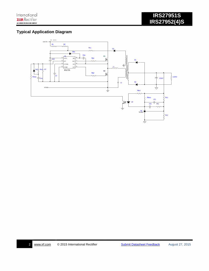
Typical Application Diagram
DC BUS
D2
Rg1
M1Cbs
Cf2
COUT
Cr
CDC
Rbias
M2
Rs1
Dss
Dbs
RT
U2
CT
Rs2
Rss
Css
Rled
Rmax
Rf2
Lr
D1
D3
U3TL431
Rg2
Cf1
Rcc
R1
RT2
CT/SD3
HO7
LO5
VB8
VCC1
COM4
VS6
U1
IRS2795
R2
LOAD
VIN
RTN
IRS27951S IRS27952(4)S
3 www.irf.com © 2015 International Rectifier Submit Datasheet Feedback August 27, 2015
Table of Contents Page
Ordering Information 1
Typical Application Diagram 2
Absolute Maximum Ratings 5
Recommended Operating Conditions 5
Electrical Characteristics 6
Functional Block Diagram 8
Input/Output Pin Equivalent Circuit Diagram 9
Lead Definitions 10
Lead Assignments 10
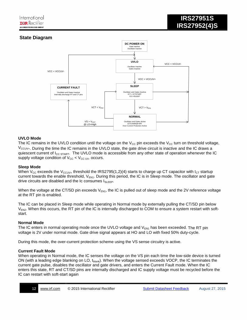
State Diagram 12
Application Information and Additional Details 13
Package Details 23
Tape and Reel Details 25
Part Marking Information 27
Qualification Information 28
IRS27951S IRS27952(4)S
4 www.irf.com © 2015 International Rectifier Submit Datasheet Feedback August 27, 2015
Description The IRS2795(1,2)(4) is a self oscillating half-bridge driver IC for DC-DC resonant converter applications, especially the LLC resonant half-bridge converter. The frequency and dead time can be programmed externally using two external components. The IC offers over current protection using the on state resistance of the low-side MOSFET. The IC can be disabled by externally pulling the voltage at the CT/SD pin below its enable voltage threshold
IRS27951S IRS27952(4)S
5 www.irf.com © 2015 International Rectifier Submit Datasheet Feedback August 27, 2015
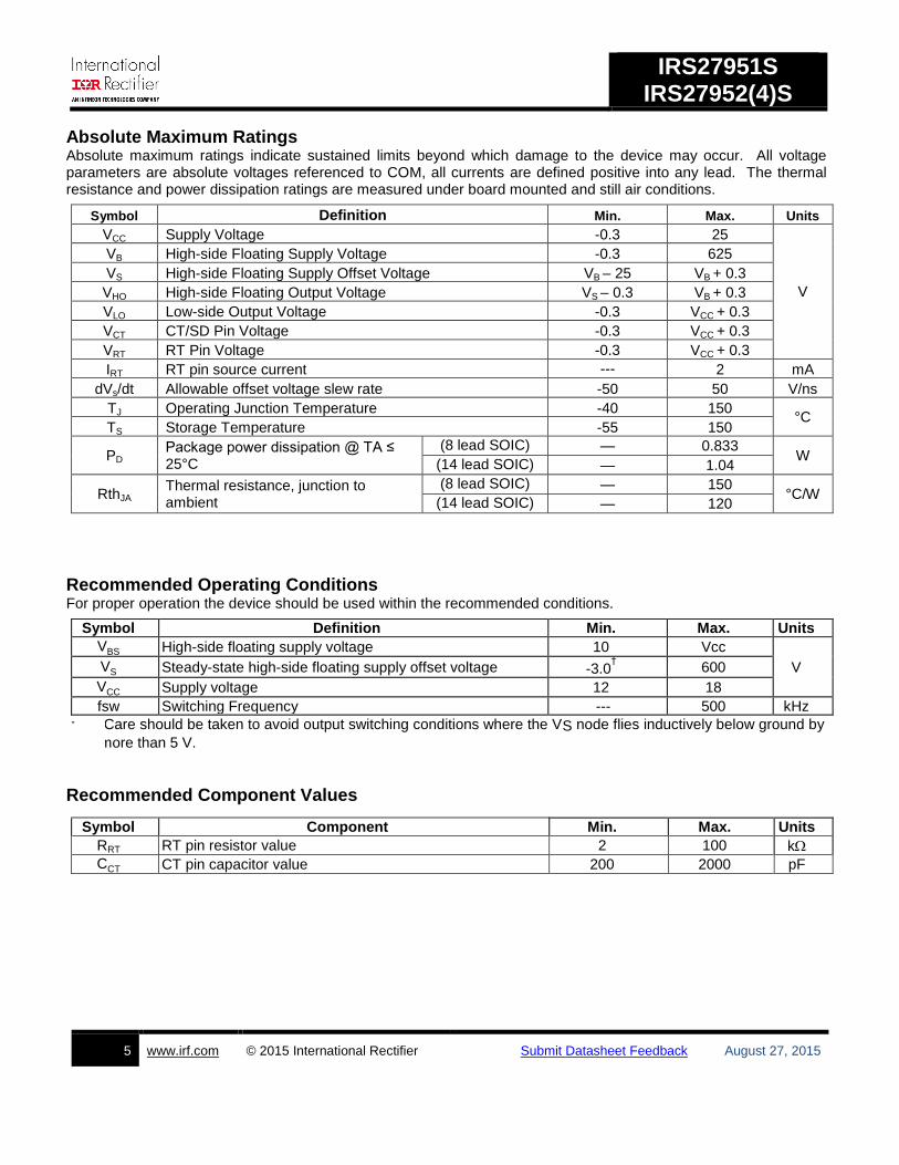
Absolute Maximum Ratings
Absolute maximum ratings indicate sustained limits beyond which damage to the device may occur. All voltage parameters are absolute voltages referenced to COM, all currents are defined positive into any lead. The thermal resistance and power dissipation ratings are measured under board mounted and still air conditions.
Symbol Definition Min. Max. Units
VCC Supply Voltage -0.3 25
V
VB High-side Floating Supply Voltage -0.3 625
VS High-side Floating Supply Offset Voltage VB – 25 VB + 0.3
VHO High-side Floating Output Voltage VS – 0.3 VB + 0.3
VLO Low-side Output Voltage -0.3 VCC + 0.3
VCT CT/SD Pin Voltage -0.3 VCC + 0.3
VRT RT Pin Voltage -0.3 VCC + 0.3
IRT RT pin source current --- 2 mA
dVs/dt Allowable offset voltage slew rate -50 50 V/ns
TJ Operating Junction Temperature -40 150 °C
TS Storage Temperature -55 150
PD Package power dissipation @ TA ≤ 25°C
(8 lead SOIC) — 0.833 W
(14 lead SOIC) — 1.04
RthJA Thermal resistance, junction to ambient
(8 lead SOIC) — 150 °C/W
(14 lead SOIC) — 120
Recommended Operating Conditions
For proper operation the device should be used within the recommended conditions.
Symbol Definition Min. Max. Units
VBS High-side floating supply voltage 10 Vcc
V
VS Steady-state high-side floating supply offset voltage -3.0† 600
VCC Supply voltage 12 18
fsw Switching Frequency --- 500 kHz
† Care should be taken to avoid output switching conditions where the VS node flies inductively below ground by
more than 5 V.
Recommended Component Values
Symbol Component Min. Max. Units
RRT RT pin resistor value 2 100 k
CCT CT pin capacitor value 200 2000 pF
IRS27951S IRS27952(4)S
6 www.irf.com © 2015 International Rectifier Submit Datasheet Feedback August 27, 2015
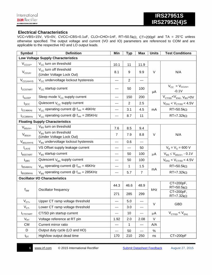
Electrical Characteristics
VCC=VBS=15V, VS=0V, CVCC=CBS=0.1uF, CLO=CHO=1nF, RT=50.5k, CT=200pF and TA = 25°C unless
otherwise specified. The output voltage and current (VO and IO) parameters are referenced to COM and are applicable to the respective HO and LO output leads.
Symbol Definition Min Typ Max Units Test Conditions
Low Voltage Supply Characteristics
VCCUV+ VCC turn on threshold 10.1 11 11.9
V N/A VCCUV- VCC turn off threshold
(Under Voltage Lock Out) 8.1 9 9.9
VCCUVHYS VCC undervoltage lockout hysteresis --- 2 ---
ICCSTART VCC startup current --- 50 100 µA
VCC = VCCUV+
-0.1V
ISLEEP Sleep mode VCC supply current --- 150 200 V
CT/SD<V
EN2, VBS=0V
IQCC Quiescent VCC supply current --- 2 2.5
mA
VEN1 < VCT/SD < 4.5V
ICC46KHz VCC operating current @ fosc = 46KHz --- 3.1 4.5 RT=50.5k
ICC285KHz VCC operating current @ fosc = 285KHz --- 8.7 11 RT=7.32k
Floating Supply Characteristics
VBSUV+ VBS turn on threshold 7.6 8.5 9.4
V N/A VBSUV- VBS turn on threshold
(Under Voltage Lock Out) 7 7.9 8.8
VBSUVHYS VBS undervoltage lockout hysteresis --- 0.6 ---
ILKVS VS Offset supply leakage current --- --- 50
A
VB = VS = 600 V
IBSSTART VBS startup current --- 50 100 VBS VBSUV+ - 0.1V
IQBS Quiescent VBS supply current --- 50 100 VEN1 < VCT/SD < 4.5V
IBS46KHz VBS operating current @ fosc = 46KHz --- 1 1.5
mA RT=50.5k
IBS285KHz VBS operating current @ fosc = 285KHz --- 5.7 7 RT=7.32k
Oscillator I/O Characteristics
fSW Oscillator frequency
44.3 46.6 48.9
kHz
CT=200pF, RT=50.5k
271 285 299 CT=200pF, RT=7.32k
VCT+ Upper CT ramp voltage threshold --- 5.0 --- V GBD
VCT- Lower CT ramp voltage threshold --- 3.0 ---
ICTSTART CT/SD pin startup current --- 10 --- A VCT/SD
< VEN1
VRT Voltage reference at RT pin 1.92 2.0 2.08 V
CM Current mirror ratio --- 1 --- A/A
D Output duty cycle (LO and HO) --- 50 --- %
tDT High/low output dead time 170 210 250 ns CT=200pF
IRS27951S IRS27952(4)S
7 www.irf.com © 2015 International Rectifier Submit Datasheet Feedback August 27, 2015
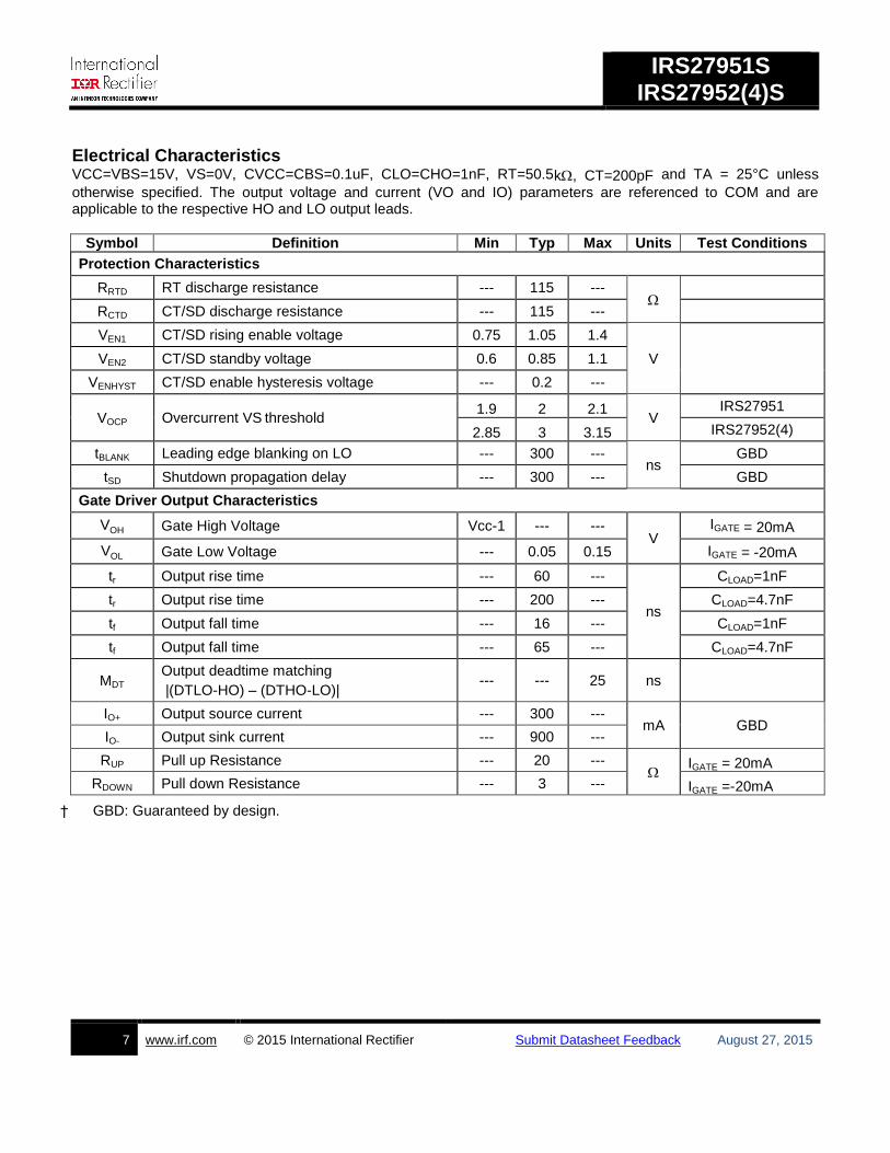
Electrical Characteristics VCC=VBS=15V, VS=0V, CVCC=CBS=0.1uF, CLO=CHO=1nF, RT=50.5k, CT=200pF and TA = 25°C unless
otherwise specified. The output voltage and current (VO and IO) parameters are referenced to COM and are applicable to the respective HO and LO output leads.
Symbol Definition Min Typ Max Units Test Conditions
Protection Characteristics
RRTD RT discharge resistance --- 115 ---
RCTD CT/SD discharge resistance --- 115 ---
VEN1 CT/SD rising enable voltage 0.75 1.05 1.4
V VEN2 CT/SD standby voltage 0.6 0.85 1.1
VENHYST CT/SD enable hysteresis voltage --- 0.2 ---
VOCP Overcurrent VS threshold 1.9 2 2.1
V IRS27951
2.85 3 3.15 IRS27952(4)
tBLANK Leading edge blanking on LO --- 300 --- ns
GBD
tSD Shutdown propagation delay --- 300 --- GBD
Gate Driver Output Characteristics
VOH Gate High Voltage Vcc-1 --- --- V
IGATE = 20mA
VOL Gate Low Voltage --- 0.05 0.15 IGATE = -20mA
tr Output rise time --- 60 ---
ns
CLOAD=1nF
tr Output rise time --- 200 --- CLOAD=4.7nF
tf Output fall time --- 16 --- CLOAD=1nF
tf Output fall time --- 65 --- CLOAD=4.7nF
MDT Output deadtime matching
|(DTLO-HO) – (DTHO-LO)| --- --- 25 ns
IO+ Output source current --- 300 --- mA GBD
IO- Output sink current --- 900 ---
RUP Pull up Resistance --- 20 ---
IGATE = 20mA
RDOWN Pull down Resistance --- 3 --- IGATE =-20mA
† GBD: Guaranteed by design.
IRS27951S IRS27952(4)S
8 www.irf.com © 2015 International Rectifier Submit Datasheet Feedback August 27, 2015
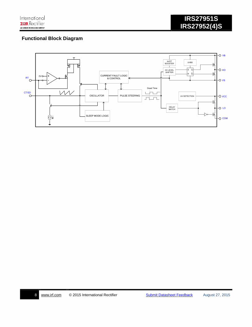
Functional Block Diagram
RT
HV LEVEL
SHIFTER
dv/DT
BOOSTERUVBS
QS
R Q
DELAY
MATCH
VB
HO
VS
COM
VCC
LO
UV DETECTION
CT/SD
OSCILLATOR
+
-
2V
SLEEP MODE LOGIC
PULSE STEERING
CURRENT FAULT LOGIC
& CONTROL
Dead Time
IRS27951S IRS27952(4)S
9 www.irf.com © 2015 International Rectifier Submit Datasheet Feedback August 27, 2015
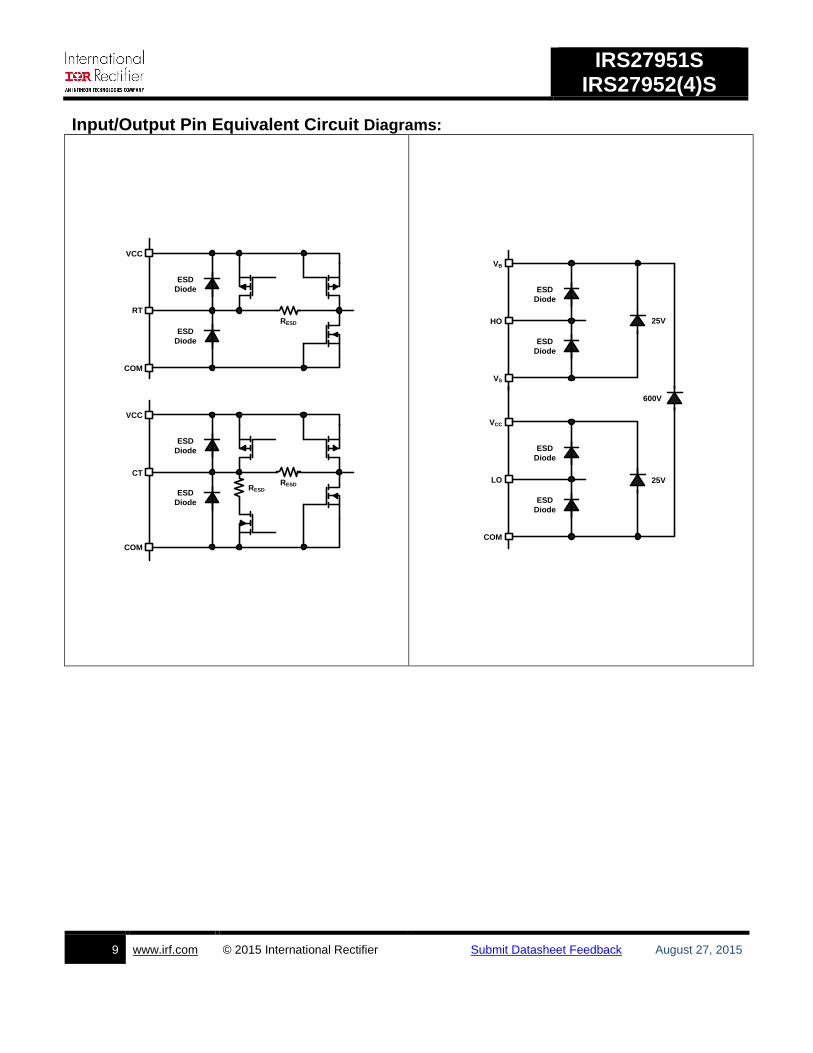
Input/Output Pin Equivalent Circuit Diagrams:
VCC
COM
RT
ESD
Diode
ESD
Diode
RESD
VCC
COM
CT
ESD
Diode
ESD
Diode
RESDRESD
VCC
COM
LO
ESD
Diode
ESD
Diode
VB
VS
HO
ESD
Diode
ESD
Diode
25V
25V
600V
IRS27951S IRS27952(4)S
10 www.irf.com © 2015 International Rectifier Submit Datasheet Feedback August 27, 2015
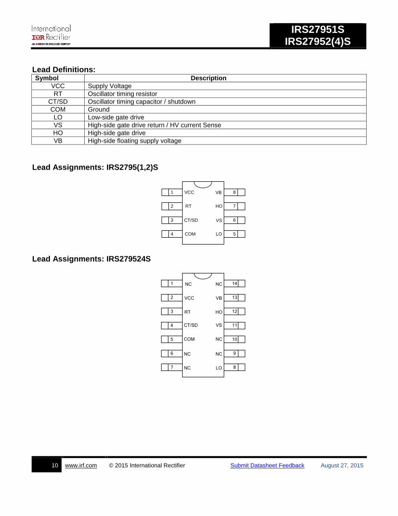
Lead Definitions: Symbol Description
VCC Supply Voltage
RT Oscillator timing resistor
CT/SD Oscillator timing capacitor / shutdown
COM Ground
LO Low-side gate drive
VS High-side gate drive return / HV current Sense
HO High-side gate drive
VB High-side floating supply voltage
Lead Assignments: IRS2795(1,2)S
HO
VB
RT
VS
VCC
CT/SD
LOCOM4
3
2
1
5
6
7
8
Lead Assignments: IRS279524S
HO
VB
COM
NC
NC
VS
7
6
5
4
3
2
1
9
10
11
12
13
14
VCC
RT
CT/SD
8
NC
NC
NC
NC
LO
IRS27951S IRS27952(4)S
11 www.irf.com © 2015 International Rectifier Submit Datasheet Feedback August 27, 2015
VCC: Power Supply Voltage This is the supply voltage pin of the IC and sense node for the under-voltage lock out circuit. It is possible to turn off the IC by pulling this pin below the minimum turn off threshold voltage, VCCUV- without damage to the IC. This pin is not internally clamped.
RT: Oscillator timing resistor This pin provides a precise 2V reference and a resistor connected from this pin to COM defines a current that is used to set the minimum oscillator frequency. To close the feedback loop that regulates the converter output voltage by modulating the oscillator frequency, the phototransistor of an optocoupler will be connected to this pin through a resistor. The value of this resistor will set the maximum operating frequency. An R-C series connected from this pin to COM sets frequency shift at start-up to prevent excessive energy inrush (soft-start). CT/SD: Oscillator timing capacitor /Shutdown An external capacitor CT from this pin to COM sets the dead time and frequency of the oscillator. The CT pin has sawtooth waveform, which is charged up by the current reference programmed at RT pin during rising slope and is discharged by an internal fixed 2mA current source during the falling slope. The falling time of the sawtooth defines the dead-time. At start-up, a 10uA current source charges this capacitor and the oscillator is enabled only when the voltage at this pin exceeds VEN1. The IC can also be used to enter sleep mode by externally pulling this pin below VEN2. COM: Logic and Gate drive Ground This is ground potential pin of the integrated control circuit. All internal circuits are referenced to this point. LO: Low-side Gate Drive Output The driver is capable of 0.3A source and 0.9A sink peak current to drive the lower MOSFET of the half-bridge leg. The pin is actively pulled to GND during UVLO. VS: High Side Gate Return/Current Sense This is the floating supply return. This pin also acts as a high voltage current sense pin and uses the low-side MOSFET RDSON to detect an over current fault condition. HO: High-side Gate Drive The driver is capable of 0.3A source and 0.9A sink peak current to drive the high-side MOSFET in the half-bridge. A resistor internally connected to pin VS ensures that the pin is not floating during UVLO. VB: High Side floating supply voltage The bootstrap capacitor connected between this pin and VS is charged by the bootstrap diode when the low-side gate-drive is high.
IRS27951S IRS27952(4)S
12 www.irf.com © 2015 International Rectifier Submit Datasheet Feedback August 27, 2015
State Diagram
UVLO Mode The IC remains in the UVLO condition until the voltage on the VCC pin exceeds the VCC turn on threshold voltage, VCCUV+. During the time the IC remains in the UVLO state, the gate drive circuit is inactive and the IC draws a quiescent current of ICC START. The UVLO mode is accessible from any other state of operation whenever the IC supply voltage condition of VCC < VCC UV- occurs. Sleep Mode When VCC exceeds the VCCUV+ threshold the IRS2795(1,2)(4) starts to charge up CT capacitor with ICT startup current towards the enable threshold, VEN1. During this period, the IC is in Sleep mode. The oscillator and gate drive circuits are disabled and the Ic consumes ISLEEP. When the voltage at the CT/SD pin exceeds VEN1, the IC is pulled out of sleep mode and the 2V reference voltage at the RT pin is enabled. The IC can be placed in Sleep mode while operating in Normal mode by externally pulling the CT/SD pin below VEN2. When this occurs, the RT pin of the IC is internally discharged to COM to ensure a system restart with soft-start. Normal Mode
The IC enters in normal operating mode once the UVLO voltage and VEN1 has been exceeded. The RT pin voltage is 2V under normal mode. Gate drive signal appears at HO and LO with fixed 50% duty-cycle. During this mode, the over-current protection scheme using the VS sense circuitry is active. Current Fault Mode When operating in Normal mode, the IC senses the voltage on the VS pin each time the low-side device is turned ON (with a leading edge blanking on LO, tblank). When the voltage sensed exceeds VOCP, the IC terminates the current gate pulse, disables the oscillator and gate drivers, and enters the Current Fault mode. When the IC enters this state, RT and CT/SD pins are internally discharged and IC supply voltage must be recycled before the IC can restart with soft-start again
DC POWER ONGate Inactive
Oscillator Inactive
UVLO
Oscillator Inactive
Gates Inactive
NORMAL
Oscillator and Gates Active
ICTCHARGE=IRT
Over Current Protection Active
VCC < VCCUV-
VS > VOCP
@ LO=High
SLEEP
Oscillator and Gates Inactive
ICT = ICTSTART
ICC=ISLEEP
VCC > VCCUV+
CURRENT FAULT
Oscillator and Gates Inactive
Internally discharge RT and CT pins
VCT > VEN1
VCC < VCCUV-
VCT < VEN2
IRS27951S IRS27952(4)S
13 www.irf.com © 2015 International Rectifier Submit Datasheet Feedback August 27, 2015
Application Information and Additional Details Information regarding the following topics is included as subsections within this section of the datasheet.
General Description
IC Supply Circuit & Low start-up current
Multi-function 2 Pin Oscillator
Frequency and Dead-time Calculation
User initiated Micropower Sleep mode
Gate Drive Capability
System Protection Features
PCB Layout Tips
Additional Documentation
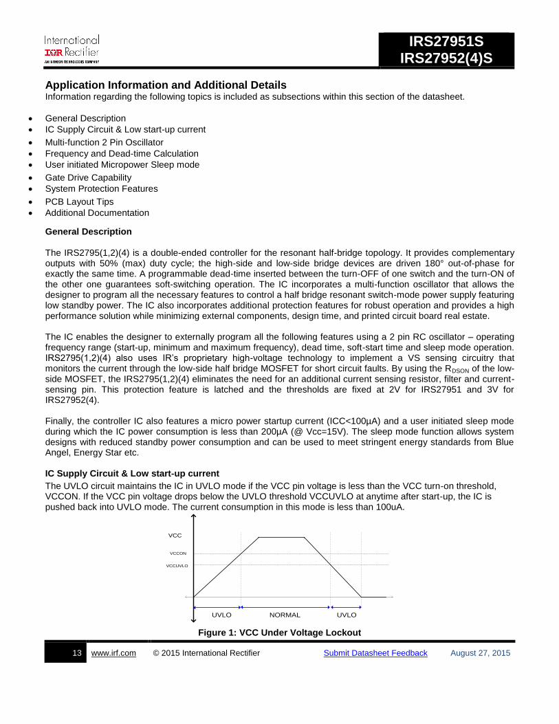
General Description The IRS2795(1,2)(4) is a double-ended controller for the resonant half-bridge topology. It provides complementary outputs with 50% (max) duty cycle; the high-side and low-side bridge devices are driven 180° out-of-phase for exactly the same time. A programmable dead-time inserted between the turn-OFF of one switch and the turn-ON of the other one guarantees soft-switching operation. The IC incorporates a multi-function oscillator that allows the designer to program all the necessary features to control a half bridge resonant switch-mode power supply featuring low standby power. The IC also incorporates additional protection features for robust operation and provides a high performance solution while minimizing external components, design time, and printed circuit board real estate. The IC enables the designer to externally program all the following features using a 2 pin RC oscillator – operating frequency range (start-up, minimum and maximum frequency), dead time, soft-start time and sleep mode operation. IRS2795(1,2)(4) also uses IR’s proprietary high-voltage technology to implement a VS sensing circuitry that monitors the current through the low-side half bridge MOSFET for short circuit faults. By using the RDSON of the low-side MOSFET, the IRS2795(1,2)(4) eliminates the need for an additional current sensing resistor, filter and current-sensing pin. This protection feature is latched and the thresholds are fixed at 2V for IRS27951 and 3V for IRS27952(4). Finally, the controller IC also features a micro power startup current (ICC<100µA) and a user initiated sleep mode during which the IC power consumption is less than 200µA (@ Vcc=15V). The sleep mode function allows system designs with reduced standby power consumption and can be used to meet stringent energy standards from Blue Angel, Energy Star etc. IC Supply Circuit & Low start-up current
The UVLO circuit maintains the IC in UVLO mode if the VCC pin voltage is less than the VCC turn-on threshold, VCCON. If the VCC pin voltage drops below the UVLO threshold VCCUVLO at anytime after start-up, the IC is pushed back into UVLO mode. The current consumption in this mode is less than 100uA.
Figure 1: VCC Under Voltage Lockout
VCC
UVLO UVLONORMAL
VCCUVLO
VCCON
IRS27951S IRS27952(4)S
14 www.irf.com © 2015 International Rectifier Submit Datasheet Feedback August 27, 2015
Multi-function 2 Pin Oscillator
The two pin oscillator is externally programmed by a resistor RT connected between pin#2 and COM and a capacitor CT, connected from pin#3 to COM. The RT pin provides an accurate 2V reference with a 2mA source capability (higher the current sourced by the pin, the higher is the oscillator frequency).
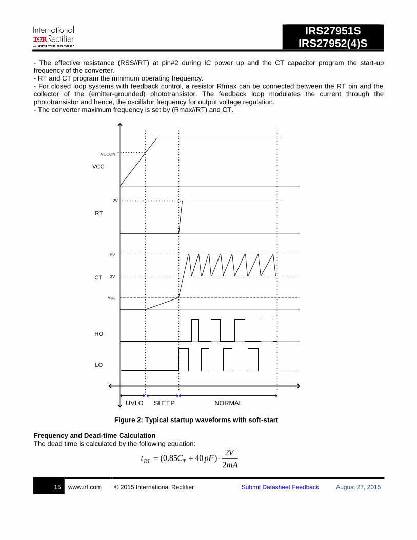
In normal operation, CT is charged by a current defined by the network connected at the RT pin. The oscillator ramp charges and discharges between the two ramp thresholds (3 and 5V). When the ramp voltage reaches 5V, it is internally discharged by a fixed current of 2mA. The fall time for the ramp corresponds to the dead time between the bridge devices.
At startup, a 10uA internal current source charges the oscillator capacitor at the CT pin to VEN1. At this point, the IC is pulled out of sleep mode and the 2V reference voltage at the RT pin is enabled. The low-side device is now also turned ON to charge the bootstrap capacitor (this sequence at startup or while exiting sleep mode ensures that the low-side device is always switched on first to charge the bootstrap capacitor which will be ready to supply the high-side floating driver). The low-side device remains ON till the CT pin voltage reaches the upper ramp threshold of 5V (see Fig 2).
The programmable features for the oscillator are listed below- • Wide frequency range: The high-speed oscillator allows an output frequency from 50 kHz up to 500 kHz. • Programmable dead-time: The oscillator timing capacitor CT also programs the dead time between LO and HO. • Programmable soft-start time: In resonant converter applications, the output power delivered is an inverse function of frequency i.e. soft- start is achieved by sweeping the operating frequency from an initial high value until the control loop takes over. Additionally, the resonant tank has a non-linear frequency dependence that makes the converter’s power transfer capability change little when the frequency is away from resonance and change very quickly as frequency approaches the resonant tank frequency.
An R-C series circuit (CSS + RSS) connected between the RT pin and COM programs the soft-start time for the converter. Initially, the capacitor CSS is totally discharged, so that the series resistor RSS is effectively in parallel to Rfmin and the resulting initial frequency is determined by RSS and RT only (the optocoupler’s phototransistor is cut off). During this frequency sweep, the operating frequency will decay following the exponential charge of CSS, that is, initially it will change relatively quickly but the rate of change will get slower. The CSS capacitor charges until its voltage reaches 2V and, consequently, the current through RSS is reduced to zero. The soft-start sequence is activated at normal startup and back to operation from Sleep mode. • Programmable start-up, minimum and maximum frequency: In resonant converter applications, it is important to operate the converter in the soft-switching region of operation. IRS2795(1,2)(4) offers a trimmed voltage reference (±4%
1) at the RT pin to accurately program the charging
current. The converter switching frequency is trimmed to be within ±5% range for the desired region of operation.
1 See revision history on the last page
IRS27951S IRS27952(4)S
15 www.irf.com © 2015 International Rectifier Submit Datasheet Feedback August 27, 2015
- The effective resistance (RSS//RT) at pin#2 during IC power up and the CT capacitor program the start-up frequency of the converter. - RT and CT program the minimum operating frequency. - For closed loop systems with feedback control, a resistor Rfmax can be connected between the RT pin and the collector of the (emitter-grounded) phototransistor. The feedback loop modulates the current through the phototransistor and hence, the oscillator frequency for output voltage regulation. - The converter maximum frequency is set by (Rmax//RT) and CT.
Figure 2: Typical startup waveforms with soft-start
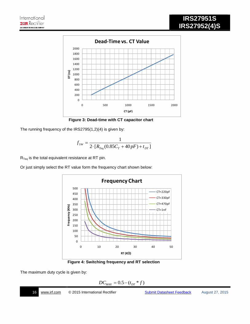
Frequency and Dead-time Calculation The dead time is calculated by the following equation:
mA
VpFCt TDT
2
2)4085.0(
SLEEP
3V
VEN1
RT
VCC
NORMALUVLO
5V
CT
2V
VCCON
HO
LO
IRS27951S IRS27952(4)S
16 www.irf.com © 2015 International Rectifier Submit Datasheet Feedback August 27, 2015
Figure 3: Dead-time with CT capacitor chart
The running frequency of the IRS2795(1,2)(4) is given by:
])4085.0([2
1
DTTTeq
SWtpFCR
f
RTeq is the total equivalent resistance at RT pin. Or just simply select the RT value form the frequency chart shown below:
Figure 4: Switching frequency and RT selection
The maximum duty cycle is given by:
)*(5.0 ftDC DTMAX
0
200
400
600
800
1000
1200
1400
1600
1800
2000
0 500 1000 1500 2000
DT
(ns)
CT (pF)
Dead-Time vs. CT Value
0
50
100
150
200
250
300
350
400
450
500
0 10 20 30 40 50
Fre
qu
en
cy (
KH
z)
RT (KΩ)
Frequency Chart
CT=220pF
CT=330pF
CT=470pF
CT=1nF
IRS27951S IRS27952(4)S
17 www.irf.com © 2015 International Rectifier Submit Datasheet Feedback August 27, 2015
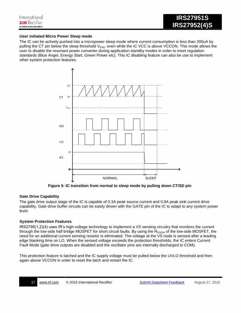
User initiated Micro Power Sleep mode
The IC can be actively pushed into a micropower sleep mode where current consumption is less than 200uA by pulling the CT pin below the sleep threshold VEN2, even while the IC VCC is above VCCON. This mode allows the user to disable the resonant power converter during application standby modes in order to meet regulation standards (Blue Angel, Energy Start, Green Power etc). This IC disabling feature can also be use to implement other system protection features.
Figure 5: IC transition from normal to sleep mode by pulling down CT/SD pin
Gate Drive Capability
The gate drive output stage of the IC is capable of 0.3A peak source current and 0.9A peak sink current drive capability. Gate drive buffer circuits can be easily driven with the GATE pin of the IC to adapt to any system power level.
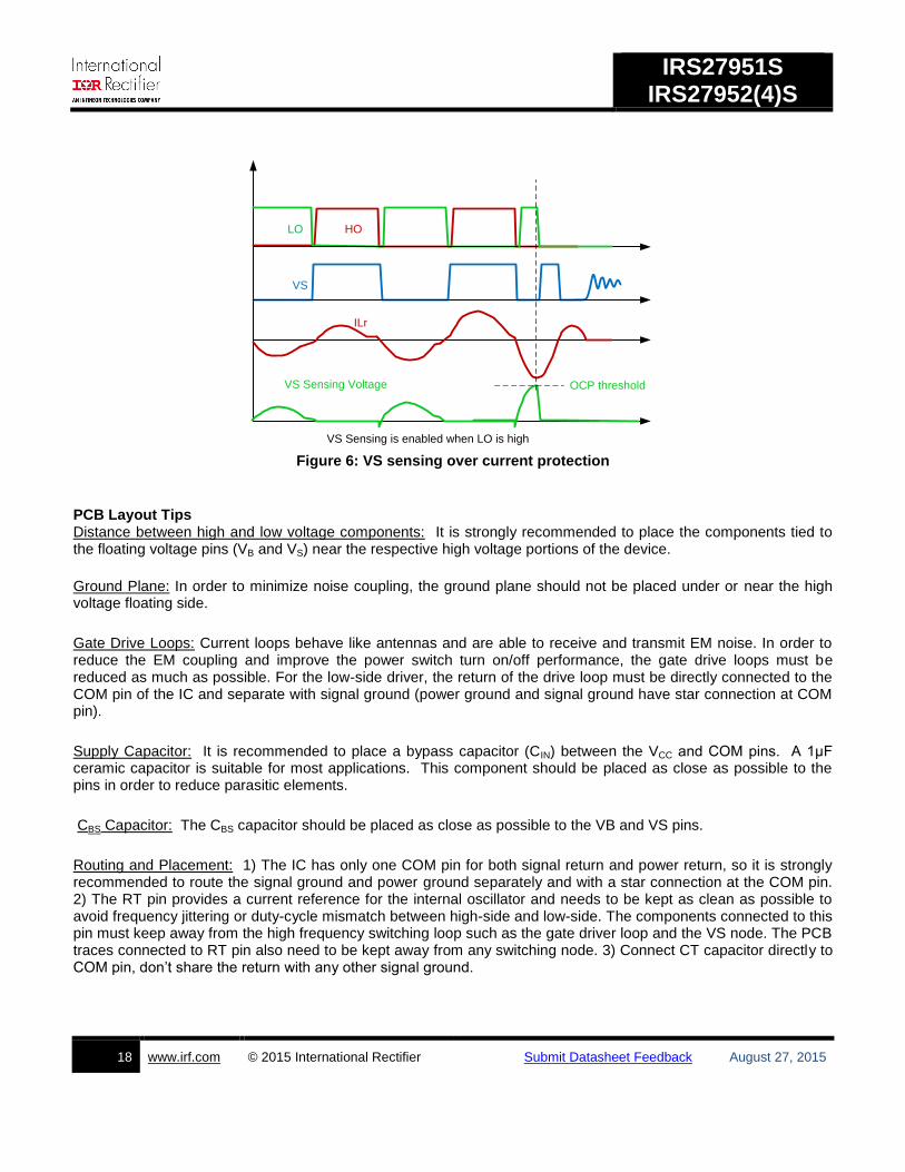
System Protection Features
IRS2795(1,2)(4) uses IR’s high-voltage technology to implement a VS sensing circuitry that monitors the current through the low-side half bridge MOSFET for short circuit faults. By using the RDSON of the low-side MOSFET, the need for an additional current sensing resistor is eliminated. The voltage at the VS node is sensed after a leading edge blanking time on LO. When the sensed voltage exceeds the protection thresholds, the IC enters Current Fault Mode (gate drive outputs are disabled and the oscillator pins are internally discharged to COM).
This protection feature is latched and the IC supply voltage must be pulled below the UVLO threshold and then again above VCCON in order to reset the latch and restart the IC.
SLEEP
3V
VEN2
NORMAL
5V
CT
2V
HO
LO
RT
IRS27951S IRS27952(4)S
18 www.irf.com © 2015 International Rectifier Submit Datasheet Feedback August 27, 2015
VS
ILr
HOLO
VS Sensing Voltage OCP threshold
VS Sensing is enabled when LO is high
Figure 6: VS sensing over current protection
PCB Layout Tips Distance between high and low voltage components: It is strongly recommended to place the components tied to the floating voltage pins (VB and VS) near the respective high voltage portions of the device.
Ground Plane: In order to minimize noise coupling, the ground plane should not be placed under or near the high voltage floating side.
Gate Drive Loops: Current loops behave like antennas and are able to receive and transmit EM noise. In order to reduce the EM coupling and improve the power switch turn on/off performance, the gate drive loops must be reduced as much as possible. For the low-side driver, the return of the drive loop must be directly connected to the COM pin of the IC and separate with signal ground (power ground and signal ground have star connection at COM pin).
Supply Capacitor: It is recommended to place a bypass capacitor (CIN) between the VCC and COM pins. A 1μF ceramic capacitor is suitable for most applications. This component should be placed as close as possible to the pins in order to reduce parasitic elements.
CBS Capacitor: The CBS capacitor should be placed as close as possible to the VB and VS pins.
Routing and Placement: 1) The IC has only one COM pin for both signal return and power return, so it is strongly recommended to route the signal ground and power ground separately and with a star connection at the COM pin. 2) The RT pin provides a current reference for the internal oscillator and needs to be kept as clean as possible to avoid frequency jittering or duty-cycle mismatch between high-side and low-side. The components connected to this pin must keep away from the high frequency switching loop such as the gate driver loop and the VS node. The PCB traces connected to RT pin also need to be kept away from any switching node. 3) Connect CT capacitor directly to COM pin, don’t share the return with any other signal ground.
IRS27951S IRS27952(4)S
19 www.irf.com © 2015 International Rectifier Submit Datasheet Feedback August 27, 2015
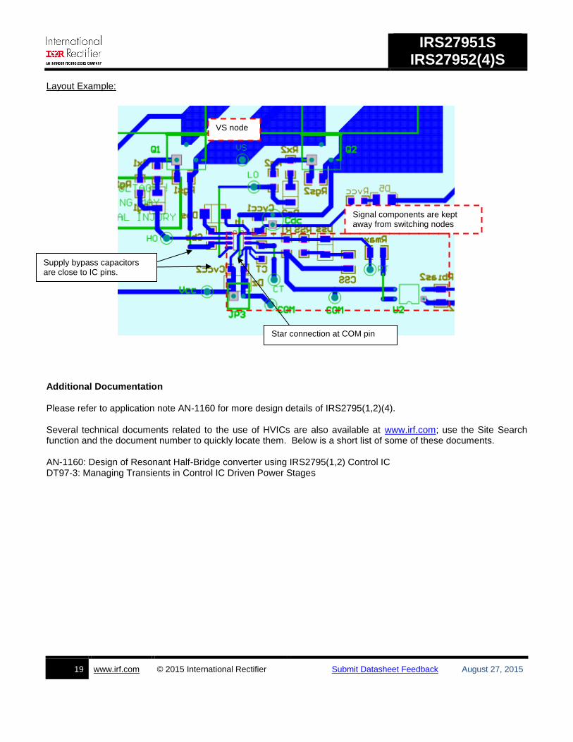
Layout Example:
Additional Documentation Please refer to application note AN-1160 for more design details of IRS2795(1,2)(4). Several technical documents related to the use of HVICs are also available at www.irf.com; use the Site Search function and the document number to quickly locate them. Below is a short list of some of these documents. AN-1160: Design of Resonant Half-Bridge converter using IRS2795(1,2) Control IC DT97-3: Managing Transients in Control IC Driven Power Stages
Supply bypass capacitors are close to IC pins.
Star connection at COM pin
Signal components are kept away from switching nodes
VS node
IRS27951S IRS27952(4)S
20 www.irf.com © 2015 International Rectifier Submit Datasheet Feedback August 27, 2015
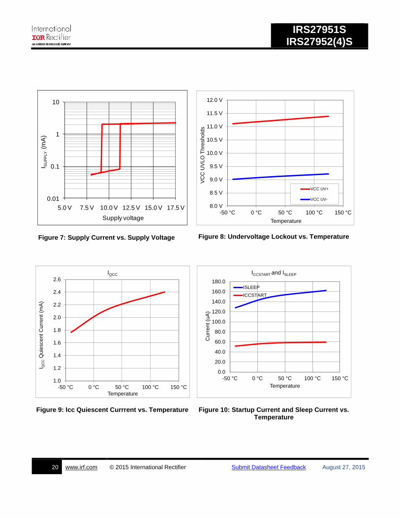
Figure 7: Supply Current vs. Supply Voltage
Figure 8: Undervoltage Lockout vs. Temperature
Figure 9: Icc Quiescent Currrent vs. Temperature
Figure 10: Startup Current and Sleep Current vs. Temperature
0.01
0.1
1
10
5.0 V 7.5 V 10.0 V 12.5 V 15.0 V 17.5 V
I SU
PP
LY
(m
A)
Supply voltage
8.0 V
8.5 V
9.0 V
9.5 V
10.0 V
10.5 V
11.0 V
11.5 V
12.0 V
-50 °C 0 °C 50 °C 100 °C 150 °C
VC
C U
VLO
Thre
shold
s
Temperature
VCC UV+
VCC UV-
1.0
1.2
1.4
1.6
1.8
2.0
2.2
2.4
2.6
-50 °C 0 °C 50 °C 100 °C 150 °C
I QC
CQ
uie
sce
nt C
urr
ent (m
A)
Temperature
IQCC
0.0
20.0
40.0
60.0
80.0
100.0
120.0
140.0
160.0
180.0
-50 °C 0 °C 50 °C 100 °C 150 °C
Cu
rre
nt (u
A)
Temperature
ICCSTART and ISLEEP
ISLEEP
ICCSTART
IRS27951S IRS27952(4)S
21 www.irf.com © 2015 International Rectifier Submit Datasheet Feedback August 27, 2015
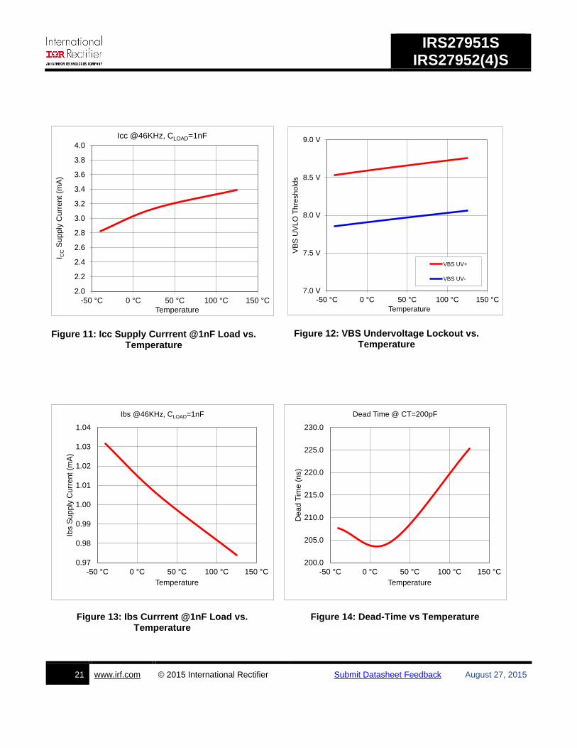
Figure 11: Icc Supply Currrent @1nF Load vs. Temperature
Figure 12: VBS Undervoltage Lockout vs. Temperature
Figure 13: Ibs Currrent @1nF Load vs. Temperature
Figure 14: Dead-Time vs Temperature
2.0
2.2
2.4
2.6
2.8
3.0
3.2
3.4
3.6
3.8
4.0
-50 °C 0 °C 50 °C 100 °C 150 °C
I CC
Su
pply
Curr
ent (m
A)
Temperature
Icc @46KHz, CLOAD=1nF
7.0 V
7.5 V
8.0 V
8.5 V
9.0 V
-50 °C 0 °C 50 °C 100 °C 150 °CV
BS
UV
LO
Thre
sh
old
s
Temperature
VBS UV+
VBS UV-
0.97
0.98
0.99
1.00
1.01
1.02
1.03
1.04
-50 °C 0 °C 50 °C 100 °C 150 °C
Ibs S
up
ply
Cu
rre
nt (m
A)
Temperature
Ibs @46KHz, CLOAD=1nF
200.0
205.0
210.0
215.0
220.0
225.0
230.0
-50 °C 0 °C 50 °C 100 °C 150 °C
Dea
d T
ime
(n
s)
Temperature
Dead Time @ CT=200pF
IRS27951S IRS27952(4)S
22 www.irf.com © 2015 International Rectifier Submit Datasheet Feedback August 27, 2015
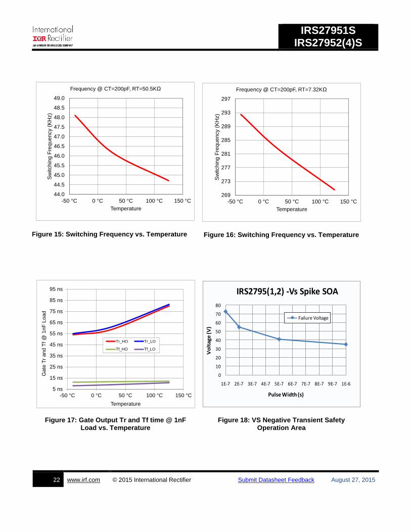
Figure 15: Switching Frequency vs. Temperature
Figure 16: Switching Frequency vs. Temperature
Figure 17: Gate Output Tr and Tf time @ 1nF Load vs. Temperature
Figure 18: VS Negative Transient Safety Operation Area
44.0
44.5
45.0
45.5
46.0
46.5
47.0
47.5
48.0
48.5
49.0
-50 °C 0 °C 50 °C 100 °C 150 °C
Sw
itchin
g F
requ
en
cy (
KH
z)
Temperature
Frequency @ CT=200pF, RT=50.5KΩ
269
273
277
281
285
289
293
297
-50 °C 0 °C 50 °C 100 °C 150 °C
Sw
itch
ing
Fre
qu
en
cy (
KH
z)
Temperature
Frequency @ CT=200pF, RT=7.32KΩ
5 ns
15 ns
25 ns
35 ns
45 ns
55 ns
65 ns
75 ns
85 ns
95 ns
-50 °C 0 °C 50 °C 100 °C 150 °C
Ga
te T
r a
nd
Tf
@ 1
nF
Lo
ad
Temperature
Tr_HO Tr_LO
Tf_HO Tf_LO
0
10
20
30
40
50
60
70
80
1E-7 2E-7 3E-7 4E-7 5E-7 6E-7 7E-7 8E-7 9E-7 1E-6
Vo
ltag
e (V
)
Pulse Width (s)
IRS2795(1,2) -Vs Spike SOA
Failure Voltage
IRS27951S IRS27952(4)S
23 www.irf.com © 2015 International Rectifier Submit Datasheet Feedback August 27, 2015
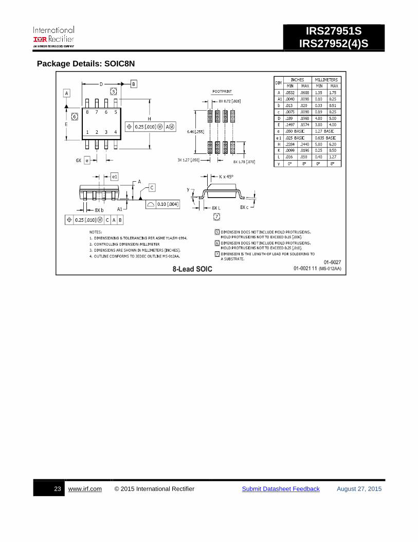
Package Details: SOIC8N
IRS27951S IRS27952(4)S
24 www.irf.com © 2015 International Rectifier Submit Datasheet Feedback August 27, 2015
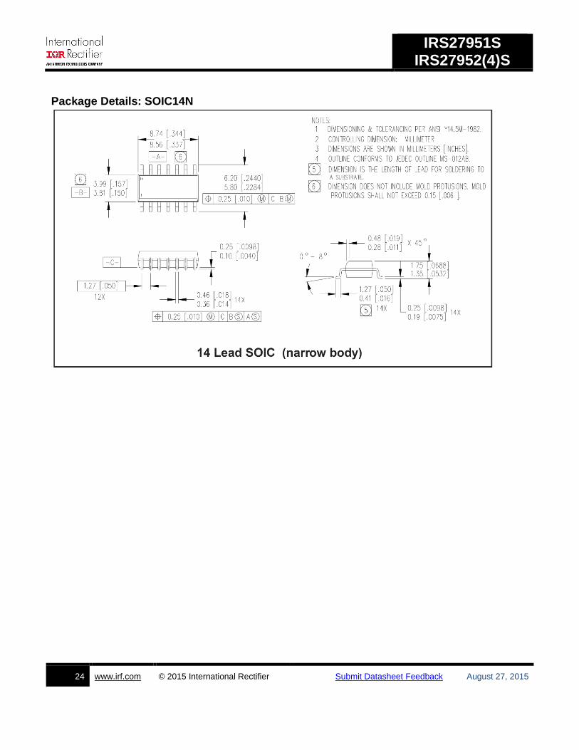
Package Details: SOIC14N
IRS27951S IRS27952(4)S
25 www.irf.com © 2015 International Rectifier Submit Datasheet Feedback August 27, 2015
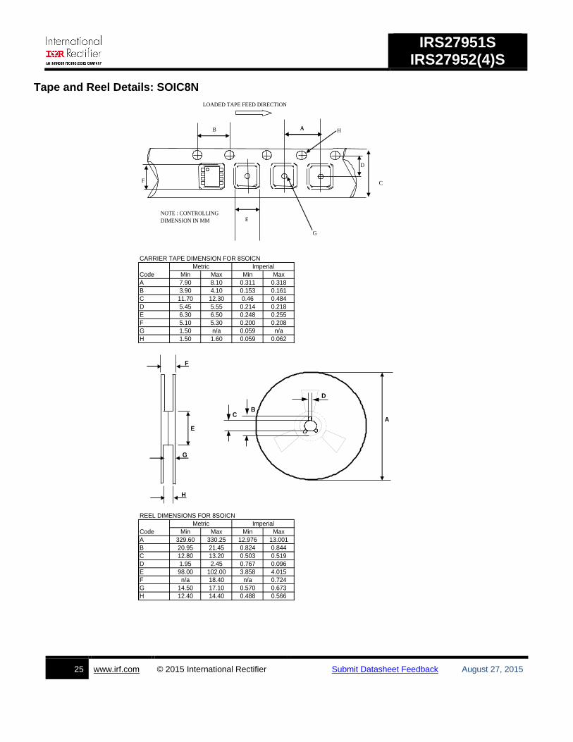
Tape and Reel Details: SOIC8N
CARRIER TAPE DIMENSION FOR 8SOICN
Code Min Max Min Max
A 7.90 8.10 0.311 0.318
B 3.90 4.10 0.153 0.161
C 11.70 12.30 0.46 0.484
D 5.45 5.55 0.214 0.218
E 6.30 6.50 0.248 0.255
F 5.10 5.30 0.200 0.208
G 1.50 n/a 0.059 n/a
H 1.50 1.60 0.059 0.062
REEL DIMENSIONS FOR 8SOICN
Code Min Max Min Max
A 329.60 330.25 12.976 13.001
B 20.95 21.45 0.824 0.844
C 12.80 13.20 0.503 0.519
D 1.95 2.45 0.767 0.096
E 98.00 102.00 3.858 4.015
F n/a 18.40 n/a 0.724
G 14.50 17.10 0.570 0.673
H 12.40 14.40 0.488 0.566
Metric Imperial
Metric Imperial
E
F
A
C
D
G
AB H
NOTE : CONTROLLING
DIMENSION IN MM
LOADED TAPE FEED DIRECTION
A
H
F
E
G
D
BC
IRS27951S IRS27952(4)S
26 www.irf.com © 2015 International Rectifier Submit Datasheet Feedback August 27, 2015
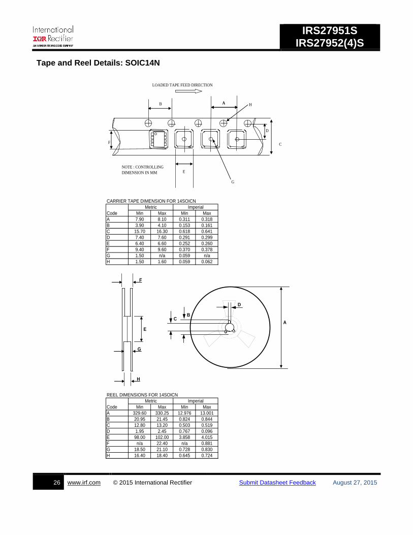
Tape and Reel Details: SOIC14N
CARRIER TAPE DIMENSION FOR 14SOICN
Code Min Max Min Max
A 7.90 8.10 0.311 0.318
B 3.90 4.10 0.153 0.161
C 15.70 16.30 0.618 0.641
D 7.40 7.60 0.291 0.299
E 6.40 6.60 0.252 0.260
F 9.40 9.60 0.370 0.378
G 1.50 n/a 0.059 n/a
H 1.50 1.60 0.059 0.062
REEL DIMENSIONS FOR 14SOICN
Code Min Max Min Max
A 329.60 330.25 12.976 13.001
B 20.95 21.45 0.824 0.844
C 12.80 13.20 0.503 0.519
D 1.95 2.45 0.767 0.096
E 98.00 102.00 3.858 4.015
F n/a 22.40 n/a 0.881
G 18.50 21.10 0.728 0.830
H 16.40 18.40 0.645 0.724
Metric Imperial
Metric Imperial
E
F
A
C
D
G
AB H
NOTE : CONTROLLING
DIMENSION IN MM
LOADED TAPE FEED DIRECTION
A
H
F
E
G
D
BC
IRS27951S IRS27952(4)S
27 www.irf.com © 2015 International Rectifier Submit Datasheet Feedback August 27, 2015
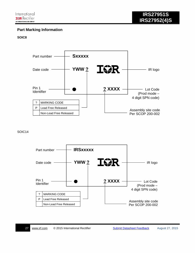
Part Marking Information
SOIC8
Sxxxxx
IR logo YWW ?
Part number
Date code
Pin 1
Identifier
Lot Code
(Prod mode –
4 digit SPN code)
Assembly site code
Per SCOP 200-002
? XXXX
MARKING CODE
Lead Free Released
Non-Lead Free Released
?
P
SOIC14
IRSxxxxx
IR logo YWW ?
Part number
Date code
Pin 1
Identifier
Lot Code
(Prod mode –
4 digit SPN code)
Assembly site code
Per SCOP 200-002
? XXXX
MARKING CODE
Lead Free Released
Non-Lead Free Released
?
P
IRS27951S IRS27952(4)S
28 www.irf.com © 2015 International Rectifier Submit Datasheet Feedback August 27, 2015
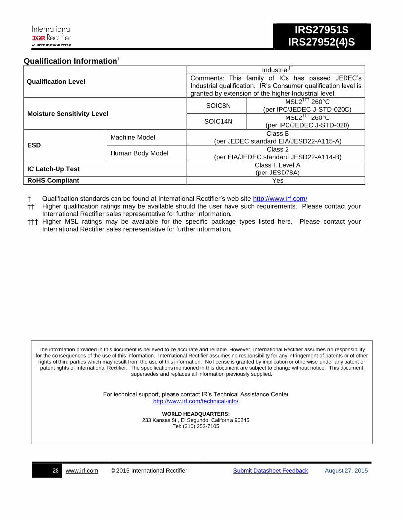
Qualification Information†
Qualification Level
Industrial††
Comments: This family of ICs has passed JEDEC’s Industrial qualification. IR’s Consumer qualification level is granted by extension of the higher Industrial level.
Moisture Sensitivity Level SOIC8N
MSL2†††
260°C (per IPC/JEDEC J-STD-020C)
SOIC14N MSL2
††† 260°C
(per IPC/JEDEC J-STD-020)
ESD Machine Model
Class B (per JEDEC standard EIA/JESD22-A115-A)
Human Body Model Class 2
(per EIA/JEDEC standard JESD22-A114-B)
IC Latch-Up Test Class I, Level A (per JESD78A)
RoHS Compliant Yes
† Qualification standards can be found at International Rectifier’s web site http://www.irf.com/ †† Higher qualification ratings may be available should the user have such requirements. Please contact your
International Rectifier sales representative for further information. ††† Higher MSL ratings may be available for the specific package types listed here. Please contact your
International Rectifier sales representative for further information.
The information provided in this document is believed to be accurate and reliable. However, International Rectifier assumes no responsibility
for the consequences of the use of this information. International Rectifier assumes no responsibility for any infringement of patents or of other rights of third parties which may result from the use of this information. No license is granted by implication or otherwise under any patent or patent rights of International Rectifier. The specifications mentioned in this document are subject to change without notice. This document
supersedes and replaces all information previously supplied.
For technical support, please contact IR’s Technical Assistance Center http://www.irf.com/technical-info/
WORLD HEADQUARTERS:
233 Kansas St., El Segundo, California 90245 Tel: (310) 252-7105
IRS27951S IRS27952(4)S
29 www.irf.com © 2015 International Rectifier Submit Datasheet Feedback August 27, 2015
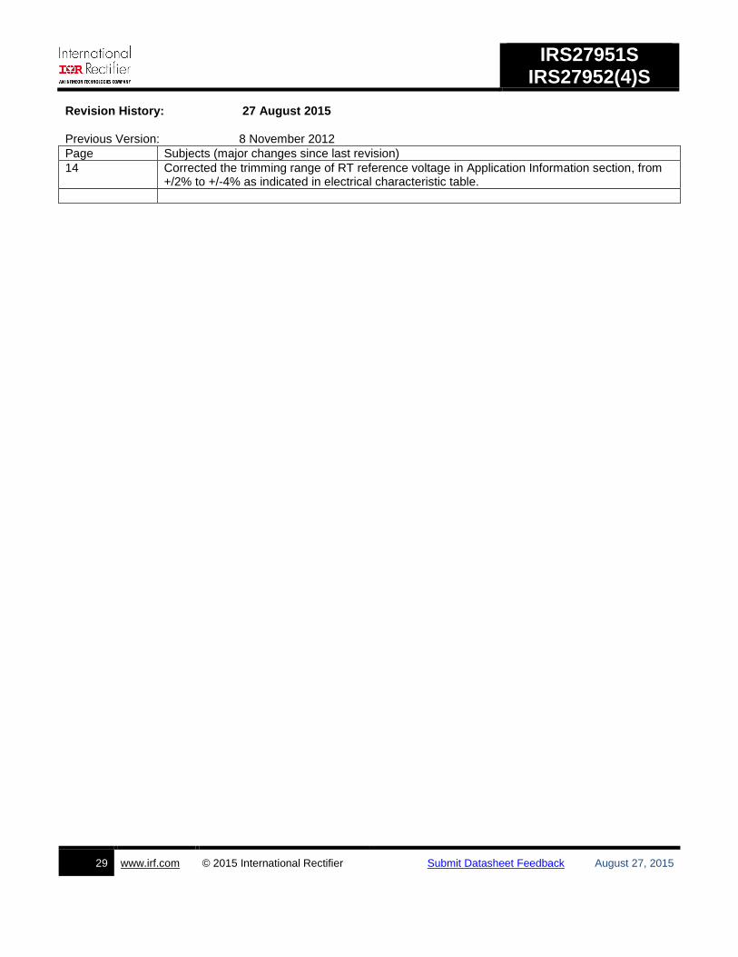
Revision History: 27 August 2015 Previous Version: 8 November 2012
Page Subjects (major changes since last revision)
14 Corrected the trimming range of RT reference voltage in Application Information section, from +/2% to +/-4% as indicated in electrical characteristic table.