Embed Size (px)
Citation preview
1
IPB65R090CFD7
Rev.2.0,2020-10-19Final Data Sheet
12
3
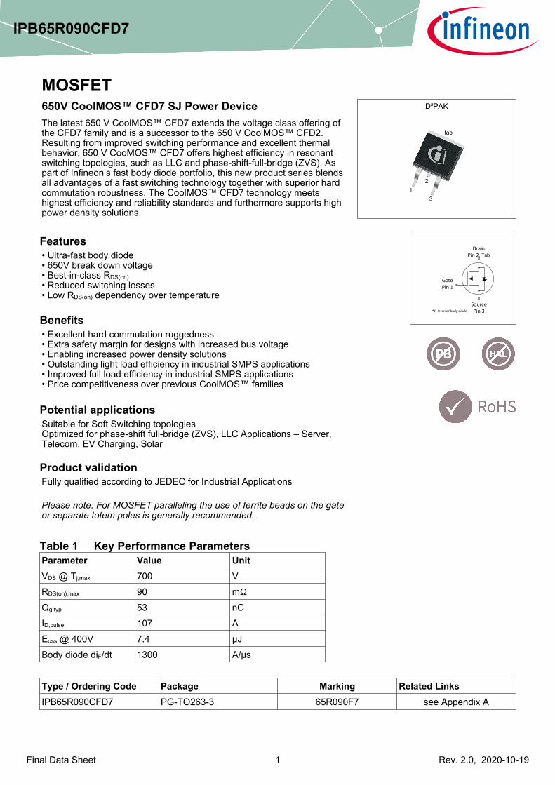
tab
D²PAK
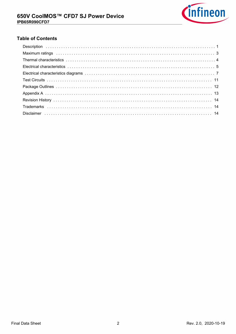
Drain
Pin 2, Tab
Gate
Pin 1
Source
Pin 3
*1
*1: Internal body diode
MOSFET650VCoolMOSªCFD7SJPowerDeviceThelatest650VCoolMOS™CFD7extendsthevoltageclassofferingoftheCFD7familyandisasuccessortothe650VCoolMOS™CFD2.Resultingfromimprovedswitchingperformanceandexcellentthermalbehavior,650VCooMOS™CFD7offershighestefficiencyinresonantswitchingtopologies,suchasLLCandphase-shift-full-bridge(ZVS).AspartofInfineon’sfastbodydiodeportfolio,thisnewproductseriesblendsalladvantagesofafastswitchingtechnologytogetherwithsuperiorhardcommutationrobustness.TheCoolMOS™CFD7technologymeetshighestefficiencyandreliabilitystandardsandfurthermoresupportshighpowerdensitysolutions.
Features•Ultra-fastbodydiode•650Vbreakdownvoltage•Best-in-classRDS(on)•Reducedswitchinglosses•LowRDS(on)dependencyovertemperature
Benefits•Excellenthardcommutationruggedness•Extrasafetymarginfordesignswithincreasedbusvoltage•Enablingincreasedpowerdensitysolutions•OutstandinglightloadefficiencyinindustrialSMPSapplications•ImprovedfullloadefficiencyinindustrialSMPSapplications•PricecompetitivenessoverpreviousCoolMOS™families
PotentialapplicationsSuitableforSoftSwitchingtopologiesOptimizedforphase-shiftfull-bridge(ZVS),LLCApplications–Server,Telecom,EVCharging,Solar
ProductvalidationFullyqualifiedaccordingtoJEDECforIndustrialApplications
Pleasenote:ForMOSFETparallelingtheuseofferritebeadsonthegateorseparatetotempolesisgenerallyrecommended.
Table1KeyPerformanceParametersParameter Value UnitVDS @ Tj,max 700 V
RDS(on),max 90 mΩ
Qg,typ 53 nC
ID,pulse 107 A
Eoss @ 400V 7.4 µJ
Body diode diF/dt 1300 A/µs
Type/OrderingCode Package Marking RelatedLinksIPB65R090CFD7 PG-TO263-3 65R090F7 see Appendix A
2
650VCoolMOSªCFD7SJPowerDeviceIPB65R090CFD7
Rev.2.0,2020-10-19Final Data Sheet
TableofContentsDescription . . . . . . . . . . . . . . . . . . . . . . . . . . . . . . . . . . . . . . . . . . . . . . . . . . . . . . . . . . . . . . . . . . . . . . . . . . . . . 1
Maximum ratings . . . . . . . . . . . . . . . . . . . . . . . . . . . . . . . . . . . . . . . . . . . . . . . . . . . . . . . . . . . . . . . . . . . . . . . . 3
Thermal characteristics . . . . . . . . . . . . . . . . . . . . . . . . . . . . . . . . . . . . . . . . . . . . . . . . . . . . . . . . . . . . . . . . . . . . 4
Electrical characteristics . . . . . . . . . . . . . . . . . . . . . . . . . . . . . . . . . . . . . . . . . . . . . . . . . . . . . . . . . . . . . . . . . . . 5
Electrical characteristics diagrams . . . . . . . . . . . . . . . . . . . . . . . . . . . . . . . . . . . . . . . . . . . . . . . . . . . . . . . . . . . 7
Test Circuits . . . . . . . . . . . . . . . . . . . . . . . . . . . . . . . . . . . . . . . . . . . . . . . . . . . . . . . . . . . . . . . . . . . . . . . . . . . 11
Package Outlines . . . . . . . . . . . . . . . . . . . . . . . . . . . . . . . . . . . . . . . . . . . . . . . . . . . . . . . . . . . . . . . . . . . . . . . 12
Appendix A . . . . . . . . . . . . . . . . . . . . . . . . . . . . . . . . . . . . . . . . . . . . . . . . . . . . . . . . . . . . . . . . . . . . . . . . . . . . 13
Revision History . . . . . . . . . . . . . . . . . . . . . . . . . . . . . . . . . . . . . . . . . . . . . . . . . . . . . . . . . . . . . . . . . . . . . . . . 14
Trademarks . . . . . . . . . . . . . . . . . . . . . . . . . . . . . . . . . . . . . . . . . . . . . . . . . . . . . . . . . . . . . . . . . . . . . . . . . . . 14
Disclaimer . . . . . . . . . . . . . . . . . . . . . . . . . . . . . . . . . . . . . . . . . . . . . . . . . . . . . . . . . . . . . . . . . . . . . . . . . . . . 14
3
650VCoolMOSªCFD7SJPowerDeviceIPB65R090CFD7
Rev.2.0,2020-10-19Final Data Sheet
1MaximumratingsatTj=25°C,unlessotherwisespecified
Table2MaximumratingsValues
Min. Typ. Max.Parameter Symbol Unit Note/TestCondition
Continuous drain current1) ID --
--
2516 A TC=25°C
TC=100°C
Pulsed drain current2) ID,pulse - - 107 A TC=25°C
Avalanche energy, single pulse EAS - - 125 mJ ID=5.0A; VDD=50V; see table 10
Avalanche energy, repetitive EAR - - 0.63 mJ ID=5.0A; VDD=50V; see table 10
Avalanche current, single pulse IAS - - 5.0 A -
MOSFET dv/dt ruggedness dv/dt - - 120 V/ns VDS=0...400VGate source voltage (static) VGS -20 - 20 V static;
Gate source voltage (dynamic) VGS -30 - 30 V AC (f>1 Hz)
Power dissipation Ptot - - 127 W TC=25°CStorage temperature Tstg -55 - 150 °C -
Operating junction temperature Tj -55 - 150 °C -
Mounting torque - - - - Ncm -
Continuous diode forward current1) IS - - 25 A TC=25°CDiode pulse current2) IS,pulse - - 107 A TC=25°C
Reverse diode dv/dt3) dv/dt - - 70 V/ns VDS=0...400V,ISD<=12.5A,Tj=25°C see table 8
Maximum diode commutation speed diF/dt - - 1300 A/µs VDS=0...400V,ISD<=12.5A,Tj=25°C see table 8
Insulation withstand voltage VISO - - n.a. V Vrms,TC=25°C,t=1min
1) Limited by Tj max.2) Pulse width tp limited by Tj,max3) Identical low side and high side switch with identical RG
4
650VCoolMOSªCFD7SJPowerDeviceIPB65R090CFD7
Rev.2.0,2020-10-19Final Data Sheet
2Thermalcharacteristics
Table3ThermalcharacteristicsValues
Min. Typ. Max.Parameter Symbol Unit Note/TestCondition
Thermal resistance, junction - case RthJC - - 0.98 °C/W -
Thermal resistance, junction - ambient RthJA - - 62 °C/W device on PCB, minimal footprint
Thermal resistance, junction - ambientfor SMD version RthJA - 35 45 °C/W
Device on 40mm*40mm*1.5mmepoxy PCB FR4 with 6cm² (onelayer, 70µm thickness) copper areafor drain connection and cooling.PCB is vertical without air streamcooling.
Soldering temperature, wavesolderingonly allowed at leads Tsold - - 260 °C reflow MSL1
5
650VCoolMOSªCFD7SJPowerDeviceIPB65R090CFD7
Rev.2.0,2020-10-19Final Data Sheet
3ElectricalcharacteristicsatTj=25°C,unlessotherwisespecified
Table4StaticcharacteristicsValues
Min. Typ. Max.Parameter Symbol Unit Note/TestCondition
Drain-source breakdown voltage V(BR)DSS 650 - - V VGS=0V,ID=1mAGate threshold voltage V(GS)th 3.5 4 4.5 V VDS=VGS,ID=0.63mA
Zero gate voltage drain current1) IDSS --
-10
137 µA VDS=650V,VGS=0V,Tj=25°C
VDS=650V,VGS=0V,Tj=125°C
Gate-source leakage current IGSS - - 100 nA VGS=20V,VDS=0V
Drain-source on-state resistance RDS(on)--
0.0680.15
0.090- Ω VGS=10V,ID=12.5A,Tj=25°C
VGS=10V,ID=12.5A,Tj=150°C
Gate resistance RG - 5.9 - Ω f=1MHz,opendrain
Table5DynamiccharacteristicsValues
Min. Typ. Max.Parameter Symbol Unit Note/TestCondition
Input capacitance Ciss - 2513 - pF VGS=0V,VDS=400V,f=250kHzOutput capacitance Coss - 40 - pF VGS=0V,VDS=400V,f=250kHz
Effective output capacitance, energyrelated2) Co(er) - 92 - pF VGS=0V,VDS=0...400V
Effective output capacitance, timerelated3) Co(tr) - 955 - pF ID=constant,VGS=0V,VDS=0...400V
Turn-on delay time td(on) - 25 - ns VDD=400V,VGS=13V,ID=12.5A,RG=5.3Ω;seetable9
Rise time tr - 11 - ns VDD=400V,VGS=13V,ID=12.5A,RG=5.3Ω;seetable9
Turn-off delay time td(off) - 92 - ns VDD=400V,VGS=13V,ID=12.5A,RG=5.3Ω;seetable9
Fall time tf - 5 - ns VDD=400V,VGS=13V,ID=12.5A,RG=5.3Ω;seetable9
Table6GatechargecharacteristicsValues
Min. Typ. Max.Parameter Symbol Unit Note/TestCondition
Gate to source charge Qgs - 14 - nC VDD=400V,ID=12.5A,VGS=0to10VGate to drain charge Qgd - 16 - nC VDD=400V,ID=12.5A,VGS=0to10VGate charge total Qg - 53 - nC VDD=400V,ID=12.5A,VGS=0to10VGate plateau voltage Vplateau - 5.7 - V VDD=400V,ID=12.5A,VGS=0to10V
1) Maximum specification is defined by calculated six sigma upper confidence bound2)Co(er)isafixedcapacitancethatgivesthesamestoredenergyasCosswhileVDSisrisingfrom0to400V3)Co(tr)isafixedcapacitancethatgivesthesamechargingtimeasCosswhileVDSisrisingfrom0to400V
6
650VCoolMOSªCFD7SJPowerDeviceIPB65R090CFD7
Rev.2.0,2020-10-19Final Data Sheet
Table7ReversediodecharacteristicsValues
Min. Typ. Max.Parameter Symbol Unit Note/TestCondition
Diode forward voltage VSD - 1.0 - V VGS=0V,IF=12.5A,Tj=25°C
Reverse recovery time trr - 147 220.5 ns VR=400V,IF=12.5A,diF/dt=100A/µs;see table 8
Reverse recovery charge Qrr - 0.78 1.56 µC VR=400V,IF=12.5A,diF/dt=100A/µs;see table 8
Peak reverse recovery current Irrm - 9.8 - A VR=400V,IF=12.5A,diF/dt=100A/µs;see table 8
7
650VCoolMOSªCFD7SJPowerDeviceIPB65R090CFD7
Rev.2.0,2020-10-19Final Data Sheet
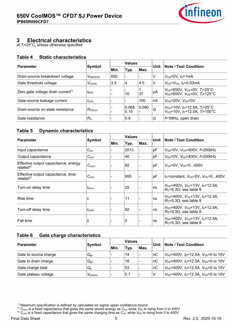
4Electricalcharacteristicsdiagrams
Diagram1:Powerdissipation
TC[°C]
Ptot[W
]
0 25 50 75 100 125 1500
25
50
75
100
125
150
Ptot=f(TC)
Diagram2:Safeoperatingarea
VDS[V]
ID[A
]
100 101 102 10310-3
10-2
10-1
100
101
102
103
1 µs
10 µs
100 µs
1 ms
10 ms
DC
ID=f(VDS);TC=25°C;D=0;parameter:tp
Diagram3:Safeoperatingarea
VDS[V]
ID[A
]
100 101 102 10310-3
10-2
10-1
100
101
102
103
1 µs
10 µs
100 µs
1 ms
10 ms
DC
ID=f(VDS);TC=80°C;D=0;parameter:tp
Diagram4:Max.transientthermalimpedance
tp[s]
ZthJC[°C/W
]
10-5 10-4 10-3 10-2 10-110-2
10-1
100
101
0.5
0.2
0.1
0.05
0.020.01
single pulse
ZthJC=f(tP);parameter:D=tp/T
8
650VCoolMOSªCFD7SJPowerDeviceIPB65R090CFD7
Rev.2.0,2020-10-19Final Data Sheet
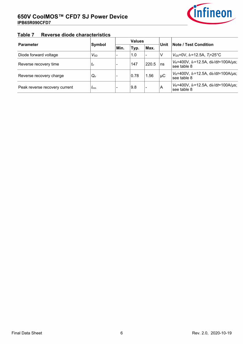
Diagram5:Typ.outputcharacteristics
VDS[V]
ID[A
]
0 5 10 15 200
40
80
120
160
200
20 V
10 V
8 V
7 V
6 V
5.5 V5 V4.5 V
ID=f(VDS);Tj=25°C;parameter:VGS
Diagram6:Typ.outputcharacteristics
VDS[V]
ID[A
]
0 5 10 15 200
25
50
75
100
125
20 V
10 V
8 V
7 V
6 V
5.5 V
5 V4.5 V
ID=f(VDS);Tj=125°C;parameter:VGS
Diagram7:Typ.drain-sourceon-stateresistance
ID[A]
RDS(on
) [Ω]
0 25 50 75 100 1250.120
0.140
0.160
0.180
0.200
20 V
10 V
7 V6.5 V6 V
5.5 V
RDS(on)=f(ID);Tj=125°C;parameter:VGS
Diagram8:Drain-sourceon-stateresistance
Tj[°C]
RDS(on
) [no
rmalized]
-50 -25 0 25 50 75 100 125 1500.5
1.0
1.5
2.0
2.5
RDS(on)=f(Tj);ID=12.5A;VGS=10V
9
650VCoolMOSªCFD7SJPowerDeviceIPB65R090CFD7
Rev.2.0,2020-10-19Final Data Sheet
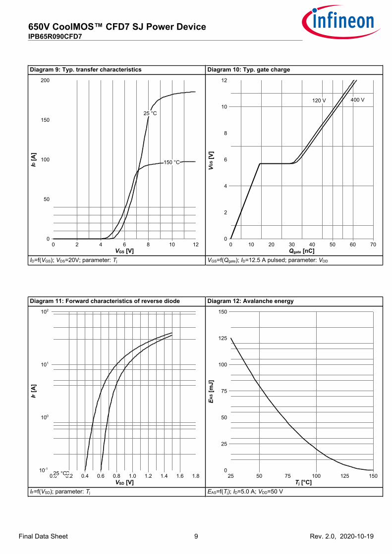
Diagram9:Typ.transfercharacteristics
VGS[V]
ID[A
]
0 2 4 6 8 10 120
50
100
150
200
150 °C
25 °C
ID=f(VGS);VDS=20V;parameter:Tj
Diagram10:Typ.gatecharge
Qgate[nC]
VGS [V]
0 10 20 30 40 50 60 700
2
4
6
8
10
12
120 V 400 V
VGS=f(Qgate);ID=12.5Apulsed;parameter:VDD
Diagram11:Forwardcharacteristicsofreversediode
VSD[V]
IF [A]
0.0 0.2 0.4 0.6 0.8 1.0 1.2 1.4 1.6 1.810-1
100
101
102
125 °C25 °C
IF=f(VSD);parameter:Tj
Diagram12:Avalancheenergy
Tj[°C]
EAS [mJ]
25 50 75 100 125 1500
25
50
75
100
125
150
EAS=f(Tj);ID=5.0A;VDD=50V
10
650VCoolMOSªCFD7SJPowerDeviceIPB65R090CFD7
Rev.2.0,2020-10-19Final Data Sheet
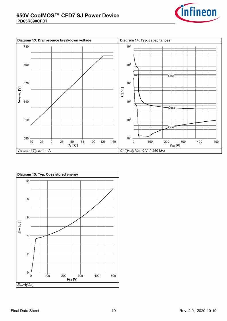
Diagram13:Drain-sourcebreakdownvoltage
Tj[°C]
VBR(DSS
) [V]
-50 -25 0 25 50 75 100 125 150580
610
640
670
700
730
VBR(DSS)=f(Tj);ID=1mA
Diagram14:Typ.capacitances
VDS[V]
C[p
F]
0 100 200 300 400 500100
101
102
103
104
105
Ciss
Coss
Crss
C=f(VDS);VGS=0V;f=250kHz
Diagram15:Typ.Cossstoredenergy
VDS[V]
Eoss[µ
J]
0 100 200 300 400 5000
2
4
6
8
10
Eoss=f(VDS)
11
650VCoolMOSªCFD7SJPowerDeviceIPB65R090CFD7
Rev.2.0,2020-10-19Final Data Sheet
5TestCircuits
Table8DiodecharacteristicsTest circuit for diode characteristics Diode recovery waveform
VDS
IF
Rg1
Rg 2
Rg1 = Rg 2
Table9SwitchingtimesSwitching times test circuit for inductive load Switching times waveform
VDS
VGS
td(on) td(off)tr
ton
tf
toff
10%
90%
VDS
VGS
Table10UnclampedinductiveloadUnclamped inductive load test circuit Unclamped inductive waveform
VDS
V(BR)DS
IDVDS
VDSID
12
650VCoolMOSªCFD7SJPowerDeviceIPB65R090CFD7
Rev.2.0,2020-10-19Final Data Sheet
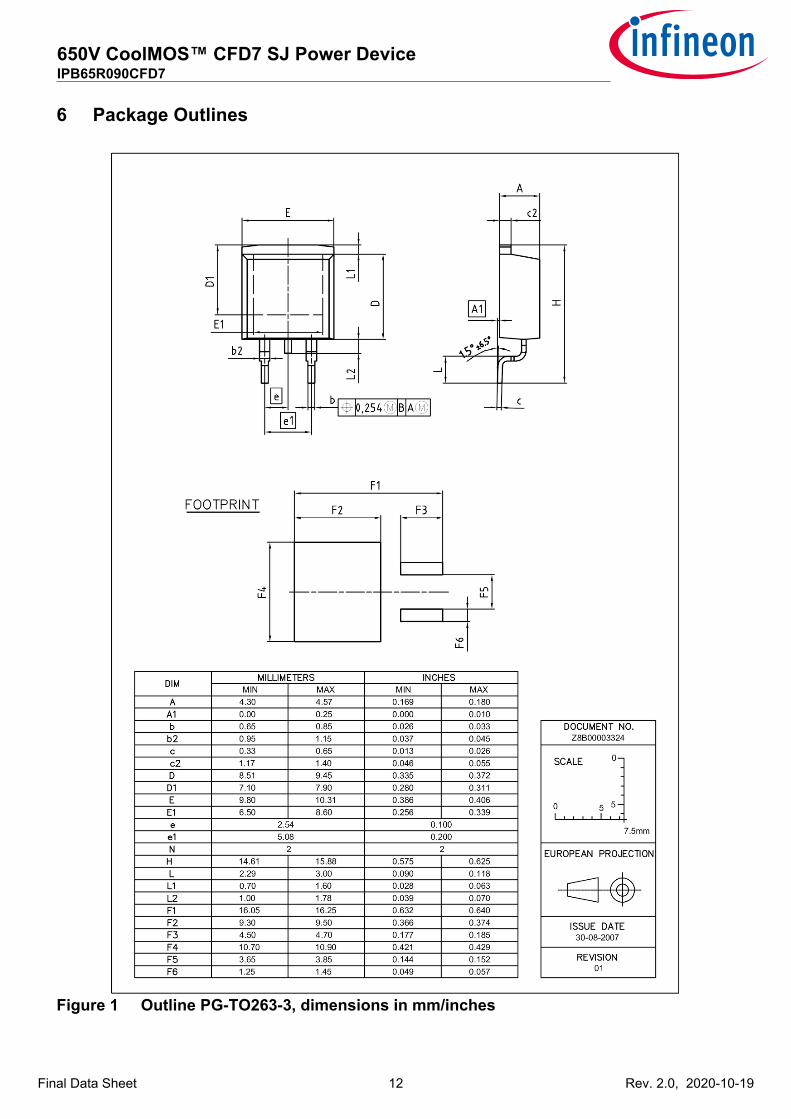
6PackageOutlines
Figure1OutlinePG-TO263-3,dimensionsinmm/inches
13
650VCoolMOSªCFD7SJPowerDeviceIPB65R090CFD7
Rev.2.0,2020-10-19Final Data Sheet
7AppendixA
Table11RelatedLinks
• IFXCoolMOSCFD7650VWebpage:www.infineon.com
• IFXCoolMOSCFD7650Vapplicationnote:www.infineon.com
• IFXCoolMOSCFD7650Vsimulationmodel:www.infineon.com
• IFXDesigntools:www.infineon.com
14
650VCoolMOSªCFD7SJPowerDeviceIPB65R090CFD7
Rev.2.0,2020-10-19Final Data Sheet
RevisionHistoryIPB65R090CFD7
Revision:2020-10-19,Rev.2.0
Previous Revision
Revision Date Subjects (major changes since last revision)
2.0 2020-10-19 Release of final version
TrademarksAllreferencedproductorservicenamesandtrademarksarethepropertyoftheirrespectiveowners.
WeListentoYourCommentsAnyinformationwithinthisdocumentthatyoufeeliswrong,unclearormissingatall?Yourfeedbackwillhelpustocontinuouslyimprovethequalityofthisdocument.Pleasesendyourproposal(includingareferencetothisdocument)to:[email protected]
PublishedbyInfineonTechnologiesAG81726München,Germany©2020InfineonTechnologiesAGAllRightsReserved.
LegalDisclaimerTheinformationgiveninthisdocumentshallinnoeventberegardedasaguaranteeofconditionsorcharacteristics(“Beschaffenheitsgarantie”).
Withrespecttoanyexamples,hintsoranytypicalvaluesstatedhereinand/oranyinformationregardingtheapplicationoftheproduct,InfineonTechnologiesherebydisclaimsanyandallwarrantiesandliabilitiesofanykind,includingwithoutlimitationwarrantiesofnon-infringementofintellectualpropertyrightsofanythirdparty.Inaddition,anyinformationgiveninthisdocumentissubjecttocustomer’scompliancewithitsobligationsstatedinthisdocumentandanyapplicablelegalrequirements,normsandstandardsconcerningcustomer’sproductsandanyuseoftheproductofInfineonTechnologiesincustomer’sapplications.Thedatacontainedinthisdocumentisexclusivelyintendedfortechnicallytrainedstaff.Itistheresponsibilityofcustomer’stechnicaldepartmentstoevaluatethesuitabilityoftheproductfortheintendedapplicationandthecompletenessoftheproductinformationgiveninthisdocumentwithrespecttosuchapplication.
InformationForfurtherinformationontechnology,deliverytermsandconditionsandpricespleasecontactyournearestInfineonTechnologiesOffice(www.infineon.com).
WarningsDuetotechnicalrequirements,componentsmaycontaindangeroussubstances.Forinformationonthetypesinquestion,pleasecontactthenearestInfineonTechnologiesOffice.TheInfineonTechnologiescomponentdescribedinthisDataSheetmaybeusedinlife-supportdevicesorsystemsand/orautomotive,aviationandaerospaceapplicationsorsystemsonlywiththeexpresswrittenapprovalofInfineonTechnologies,ifafailureofsuchcomponentscanreasonablybeexpectedtocausethefailureofthatlife-support,automotive,aviationandaerospacedeviceorsystemortoaffectthesafetyoreffectivenessofthatdeviceorsystem.Lifesupportdevicesorsystemsareintendedtobeimplantedinthehumanbodyortosupportand/ormaintainandsustainand/orprotecthumanlife.Iftheyfail,itisreasonabletoassumethatthehealthoftheuserorotherpersonsmaybeendangered.