Embed Size (px)
Citation preview
1TNF
Texas Nanofabrication Facility (TNF)
• Cleanroom nanofab capabilities, nano-metrology and nanomanufacturing with ~130 major tools, and ~30 staff
• Located at University of Texas at Austin– Microelectronics Research Center (cleanroom fab for nano)S.K. Banerjee- Site Director; S.Majumder- Coordinator
– Texas Materials Institute (nanometrology)R.Manthiram
– NASCENT ERC (nanoimprint and roll-to-roll nanomanufacturing)S.V. Sreenivasan
– SEIL.A. Kahlor
2TNF
TNF: Facilities and Tools
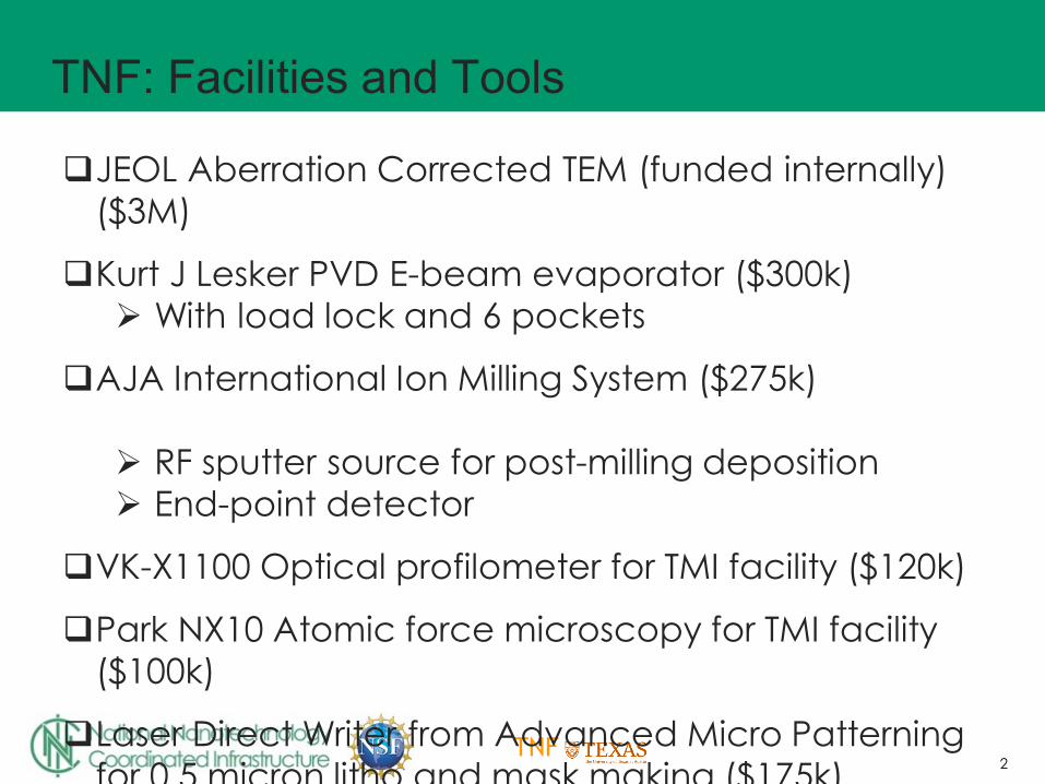
JEOL Aberration Corrected TEM (funded internally) ($3M)
Kurt J Lesker PVD E-beam evaporator ($300k) With load lock and 6 pockets
AJA International Ion Milling System ($275k)
RF sputter source for post-milling deposition End-point detector
VK-X1100 Optical profilometer for TMI facility ($120k)
Park NX10 Atomic force microscopy for TMI facility ($100k)
Laser Direct Writer from Advanced Micro Patterning for 0 5 micron litho and mask making ($175k)
3TNF
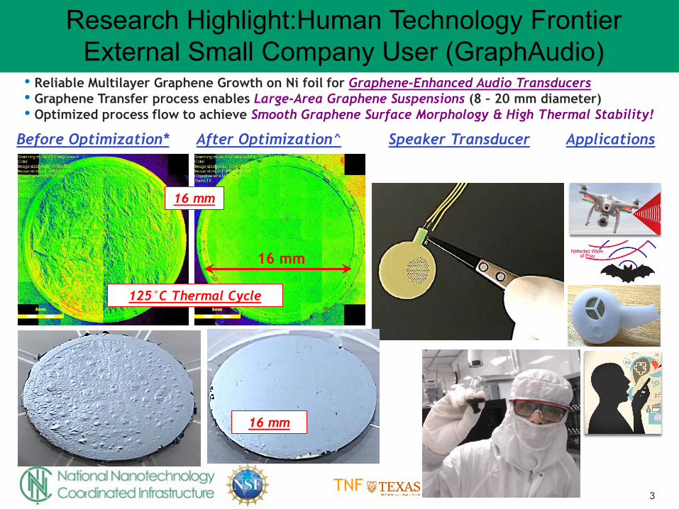
• Reliable Multilayer Graphene Growth on Ni foil for Graphene-Enhanced Audio Transducers• Graphene Transfer process enables Large-Area Graphene Suspensions (8 – 20 mm diameter)• Optimized process flow to achieve Smooth Graphene Surface Morphology & High Thermal Stability!
Research Highlight:Human Technology FrontierExternal Small Company User (GraphAudio)
Before Optimization* After Optimization^ Speaker Transducer Applications
16 mm
125°C Thermal Cycle
16 mm
16 mm
*Pre
4TNF
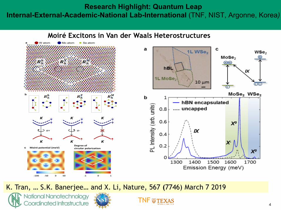
Research Highlight: Quantum LeapInternal-External-Academic-National Lab-International (TNF, NIST, Argonne, Korea)
K. Tran, … S.K. Banerjee… and X. Li, Nature, 567 (7746) March 7 2019
a
b
W atom Mo atom Se atom
σ+
K
K
σ-
K
K
K
Kc
-100 -50 0 50
Moiré potential (meV)
-1 0 1
Degree ofcircular polarization
Moiré Excitons in Van der Waals Heterostructures
5TNF
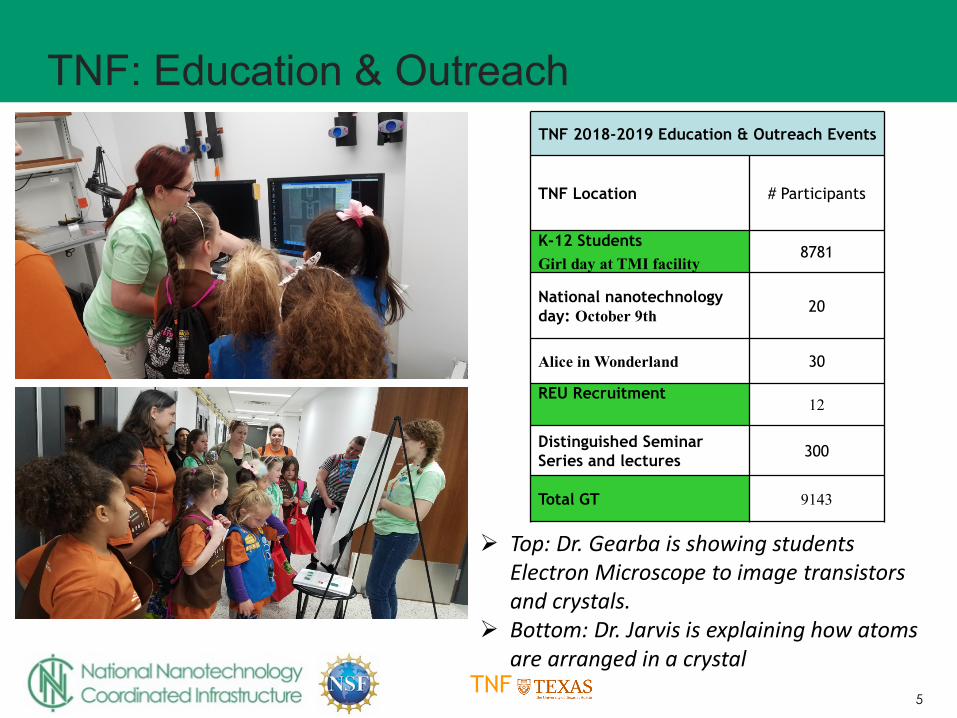
TNF: Education & OutreachTNF 2018-2019 Education & Outreach Events
TNF Location # Participants
K-12 StudentsGirl day at TMI facility
8781
National nanotechnology day: October 9th 20
Alice in Wonderland 30
REU Recruitment12
Distinguished Seminar Series and lectures 300
Total GT 9143
Top: Dr. Gearba is showing students Electron Microscope to image transistors and crystals.
Bottom: Dr. Jarvis is explaining how atoms are arranged in a crystal
6TNF
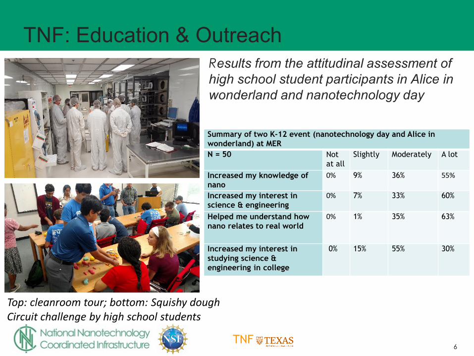
TNF: Education & OutreachResults from the attitudinal assessment of high school student participants in Alice in wonderland and nanotechnology day
Summary of two K-12 event (nanotechnology day and Alice in wonderland) at MERN = 50 Not
at allSlightly Moderately A lot
Increased my knowledge of nano
0% 9% 36% 55%
Increased my interest in science & engineering
0% 7% 33% 60%
Helped me understand how nano relates to real world
0% 1% 35% 63%
Increased my interest in studying science & engineering in college
0% 15% 55% 30%
Top: cleanroom tour; bottom: Squishy dough Circuit challenge by high school students
7TNF
TNF: Societal and Ethical Implications (L.A.Kahlor)
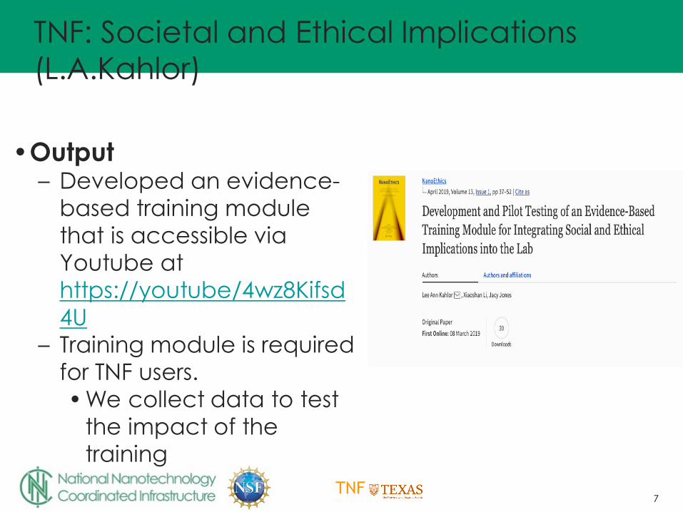
•Output– Developed an evidence-
based training modulethat is accessible via Youtube at https://youtube/4wz8Kifsd4U
– Training module is required for TNF users.• We collect data to test
the impact of the training
8TNF
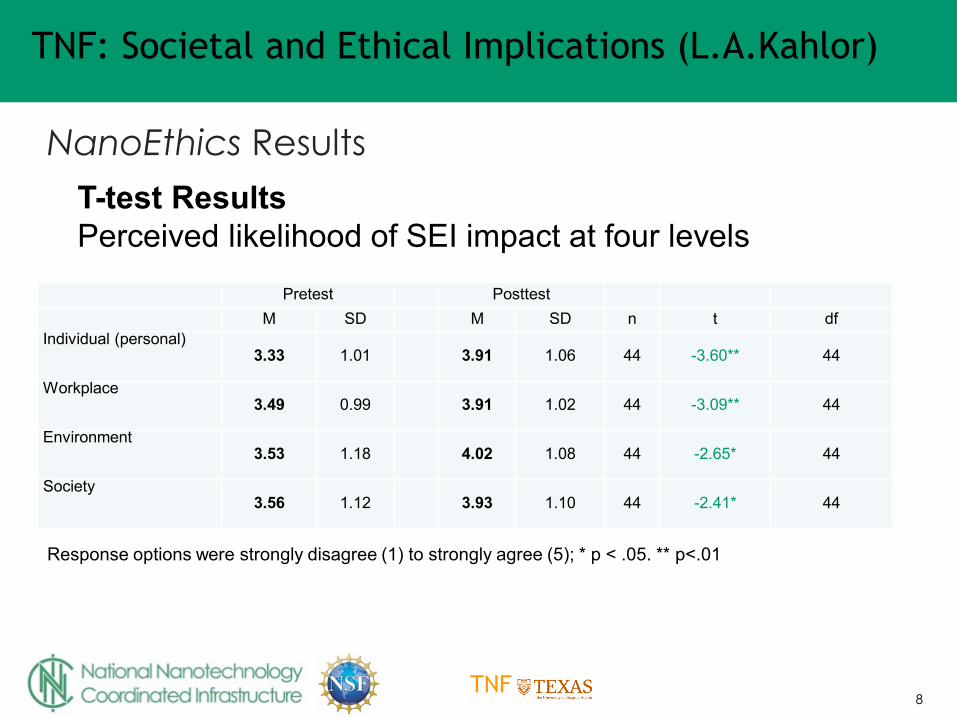
NanoEthics Results
Pretest PosttestM SD M SD n t df
Individual (personal)3.33 1.01 3.91 1.06 44 -3.60** 44
Workplace3.49 0.99 3.91 1.02 44 -3.09** 44
Environment3.53 1.18 4.02 1.08 44 -2.65* 44
Society3.56 1.12 3.93 1.10 44 -2.41* 44
T-test ResultsPerceived likelihood of SEI impact at four levels
Response options were strongly disagree (1) to strongly agree (5); * p < .05. ** p<.01
TNF: Societal and Ethical Implications (L.A.Kahlor)
9TNF
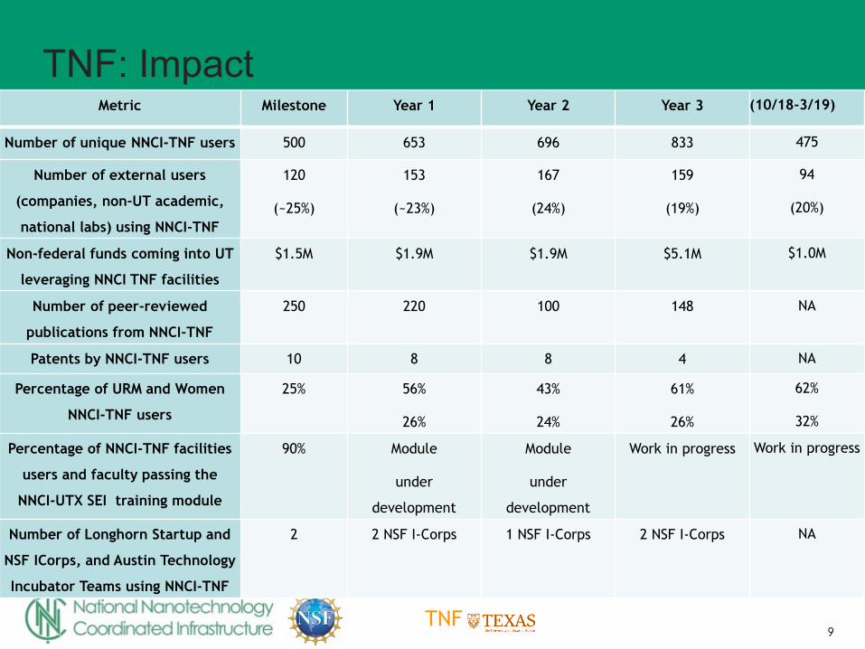
TNF: ImpactMetric Milestone Year 1 Year 2 Year 3 (10/18-3/19)
Number of unique NNCI-TNF users 500 653 696 833 475
Number of external users
(companies, non-UT academic,
national labs) using NNCI-TNF
120
(~25%)
153
(~23%)
167
(24%)
159
(19%)
94
(20%)
Non-federal funds coming into UT
leveraging NNCI TNF facilities
$1.5M $1.9M $1.9M $5.1M $1.0M
Number of peer-reviewed
publications from NNCI-TNF
250 220 100 148 NA
Patents by NNCI-TNF users 10 8 8 4 NA
Percentage of URM and Women
NNCI-TNF users
25% 56%
26%
43%
24%
61%
26%
62%
32%
Percentage of NNCI-TNF facilities
users and faculty passing the
NNCI-UTX SEI training module
90% Module
under
development
Module
under
development
Work in progress Work in progress
Number of Longhorn Startup and
NSF ICorps, and Austin Technology
Incubator Teams using NNCI-TNF
2 2 NSF I-Corps 1 NSF I-Corps 2 NSF I-Corps NA
10TNF
TNF: Network Collaboration (TNF, SDNI and CNF)
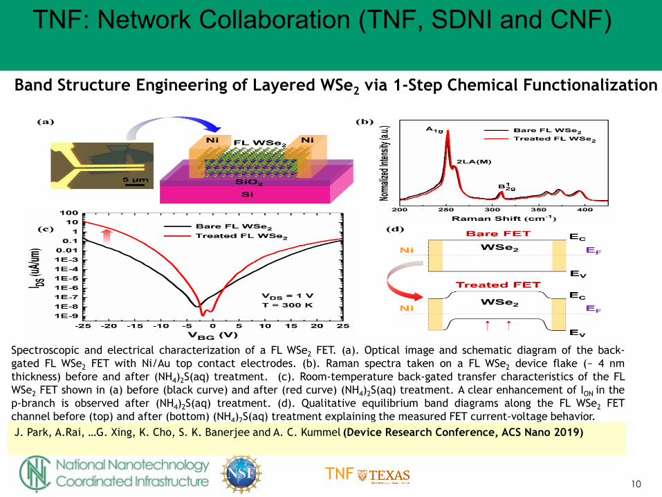
Spectroscopic and electrical characterization of a FL WSe2 FET. (a). Optical image and schematic diagram of the back-gated FL WSe2 FET with Ni/Au top contact electrodes. (b). Raman spectra taken on a FL WSe2 device flake (~ 4 nmthickness) before and after (NH4)2S(aq) treatment. (c). Room-temperature back-gated transfer characteristics of the FLWSe2 FET shown in (a) before (black curve) and after (red curve) (NH4)2S(aq) treatment. A clear enhancement of ION in thep-branch is observed after (NH4)2S(aq) treatment. (d). Qualitative equilibrium band diagrams along the FL WSe2 FETchannel before (top) and after (bottom) (NH4)2S(aq) treatment explaining the measured FET current-voltage behavior.J. Park, A.Rai, …G. Xing, K. Cho, S. K. Banerjee and A. C. Kummel (Device Research Conference, ACS Nano 2019)
Band Structure Engineering of Layered WSe2 via 1-Step Chemical Functionalization
11TNF
TNF: Network Collaboration
• L.A. Kahlor interacts with other sites on SEI.
• S. Banerjee serves on the NNCI Metrics sub-committee
• S. Majumder serves on the etch-committee.
• TNF staff have participated in various technical workshops that were organized (ALD- Harvard and Stanford, Etch- Cornell and Stanford, EBL-Georgia Tech, Soft Lithography- Harvard).