Embed Size (px)
Citation preview
483
r e v i e w
international Journal of Nanomedicine 2006:1(4) 483–495© 2006 Dove Medical Press Limited. All rights reserved
Abstract: Micro- and nanofabrication techniques have revolutionized the pharmaceutical
and medical fields as they offer the possibility for highly reproducible mass-fabrication of
systems with complex geometries and functionalities, including novel drug delivery systems
and bionsensors. The principal micro- and nanofabrication techniques are described, including
photolithography, soft lithography, film deposition, etching, bonding, molecular self assembly,
electrically induced nanopatterning, rapid prototyping, and electron, X-ray, colloidal monolayer,
and focused ion beam lithography. Application of these techniques for the fabrication of
drug delivery and biosensing systems including injectable, implantable, transdermal, and
mucoadhesive devices is described.
Keywords: microfabrication, nanofabrication, medical devices, drug delivery, biosensors
IntroductionMicro- and nanodevices have many advantages over their macroscale counterparts.
For instance, miniaturization allows for the manufacture of portable, hand-held,
implantable, or even injectable devices. In addition, as a result of their minute size,
these devices need less sample or reagent for analysis or operation, saving money and
time. Moreover, where materials and/or processes are inhibited by lengthy diffusion
times, miniaturization provides a mechanism for abbreviating these. A notable
example where these microdevices allow for significant advantages over traditional
technologies is in medical care. For example, point-of-care diagnostic testing, which
is testing performed at the patient’s bedside, permits physicians to diagnose a patient’s
conditions more rapidly than conventional lab-based testing. By using these devices to
reduce the time to diagnoses, the physician is able to make better patient management
decisions leading to improved patient outcomes and reduce the overall cost of care.
Advances in microelectronics and biosensor tools have been instrumental in facilitating
the development of these point-of-care diagnostic devices.
Microfabrication techniques were developed for applications in the semiconductor
industry and are, consequently, not specific for biological or medical applications.
Nonetheless, both micro- and nanofabrication have offered a number of possibilities for
the study of chemical, biological, and physical processes at the cellular and molecular
scale, and for the design of synthetic devices capable of interacting with biological
systems at these levels.
Some of the advantages of micro- and nanofabricated devices include the ability
to control the features to the nanometer scale for reproducible mass production of
structures and devices, the ability to miniaturize already-existing systems for the study
of cellular or molecular processes, the capacity of including electronics within structural
devices through the use of the well-developed semiconductor techniques, and the high
throughput possible with some of the micro- and nanofabrication methods.
Tania BetancourtLisa Brannon-Peppas
Department of Biomedical engineering, The University of Texas at Austin, TX, USA
Correspondence: Lisa Brannon-Peppas Department of Biomedical engineering, The University of Texas at Austin, 1 University Station C0300, Austin, TX 78712, USA Tel +1 512 471 4348 Fax +1 512 471 4348 email [email protected]
Micro- and nanofabrication methods in nanotechnological medical and pharmaceutical devices
international Journal of Nanomedicine 2006:1(4)484
Betancourt and Brannon-Peppas
The integration of the knowledge gained from micro- and
nano-fabrication can lead to design principles for nanodevices
that can detect substances, analyze their environment, and
perform tasks such as the release of a specific molecule. These
vehicles will combine responsive polymers, nanoparticles,
nucleotides, and micro-electromechanical systems (MEMS)
elements.
Expertise in combining MEMS systems with environ-
mentally sensitive polymers has led to the design of controlled
release systems. For example, research in physiologically
responsive materials shows how it is possible to design
devices which are responsive to changes in the surrounding
environment. Biological molecular recognition systems
have been used widely in designing novel devices such as
DNA-fueled molecular machines (Seeman 2003; Yurke et
al 2003), tailored colloidal aggregates, and biomolecular
nanomechanical sensors. We have also expertise in the
controlled release of therapeutics, and in modifying
the targeting and release properties of biodegradable
nanoparticles (Blanchette et al 2004; Brannon-Peppas and
Blanchette 2004). It will be important to integrate MEMS
technology into the biological environment, as with polymeric
nanoparticle delivery systems, and microfabricated nano- and
microcontainers with responsive delivery systems (sensor-
controlled delivery).
Finally, investigation of intelligent nanoscale systems
with the ability of the molecules themselves to make
decisions is needed in our field. Nucleic acids are likely
the best candidates for sensing, transducing, deciding, and
treating, as demonstrated by nucleic acid “gates” that can
sense analytes, integrate information, and carry out reactions
that would in turn lead to the release of therapeutic molecules,
such as siRNAs. By integrating these technologies with novel
drug delivery methods, it should prove possible to make
extremely “smart” therapeutics.
This review focuses on the diverse micro- and nanofabri-
cation techniques available, and on the applications of these
techniques into the construction of devices for medical
applications. However, because of the vast number of
techniques that have been developed in the recent years
for very specific applications, this review is by no means
exhaustive.
Microfabrication techniquesA number of techniques are used for the fabrication of
micron-scale devices. Some of these techniques have been
adopted from the well-established field of semiconductors,
but others have been specifically developed for microfabrica-
tion. The microfabrication process utilizes these techniques in
a sequential manner to produce the desired structure. These
structures can be built within the bulk of a substrate material
in what is known as bulk micromachining, or on the surface
of the substrate through surface micromachining (Voldman
et al 1999). In most cases, however, a combination of bulk
and surface micromachining is utilized in the fabrication of
the desired system.
The most important microfabrication techniques are
photolithography, soft lithography, film deposition, etching,
and bonding. Photolithography is used to transfer a user-
generated shape onto a material through the selective
exposure of a light sensitive polymer. Soft lithography
encompasses three different techniques which are all based on
the generation and utilization of the mold of a microstructure
out of poly(dimethylsiloxane). Film deposition, as its name
suggest, consists of the formation of micron-thick films on the
surface of a substrate. Etching selectively removes materials
from the surface of the microdevice by either chemical or
physical processes. Finally, bonding adheres substrates
together with or without the use of intermediary layers. The
following section will discuss these and other techniques in
more detail.
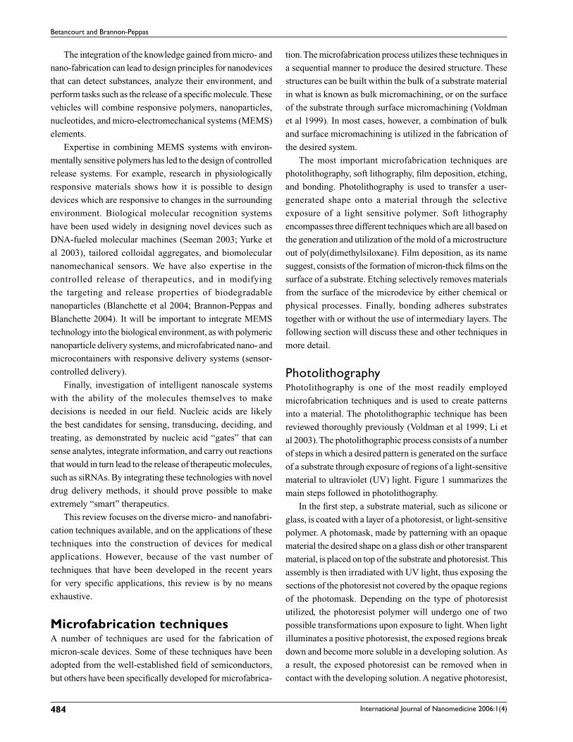
PhotolithographyPhotolithography is one of the most readily employed
microfabrication techniques and is used to create patterns
into a material. The photolithographic technique has been
reviewed thoroughly previously (Voldman et al 1999; Li et
al 2003). The photolithographic process consists of a number
of steps in which a desired pattern is generated on the surface
of a substrate through exposure of regions of a light-sensitive
material to ultraviolet (UV) light. Figure 1 summarizes the
main steps followed in photolithography.
In the first step, a substrate material, such as silicone or
glass, is coated with a layer of a photoresist, or light-sensitive
polymer. A photomask, made by patterning with an opaque
material the desired shape on a glass dish or other transparent
material, is placed on top of the substrate and photoresist. This
assembly is then irradiated with UV light, thus exposing the
sections of the photoresist not covered by the opaque regions
of the photomask. Depending on the type of photoresist
utilized, the photoresist polymer will undergo one of two
possible transformations upon exposure to light. When light
illuminates a positive photoresist, the exposed regions break
down and become more soluble in a developing solution. As
a result, the exposed photoresist can be removed when in
contact with the developing solution. A negative photoresist,
international Journal of Nanomedicine 2006:1(4) 485
Micro- and nanofabrication in biomedical devices
on the other hand, becomes crosslinked upon exposure to
light, thus becoming insoluble in the developing solution.
Consequently, upon contact with the developing solution,
only the parts not exposed to light will be removed.
The resulting photoresist patterns are then used to protect
the covered substrate from etching, or from the deposition of
compounds or biomolecules on its surface. After the desired
process is completed, the photoresist can be removed, leaving
the pattern design on the substrate. The technique used for
photoresist removal usually consists of sonication in an
organic solvent, and may consequently be undesirable for
a number of systems, specially those containing biological
molecules. As an alternative, water-soluble photoresists have
been developed; however, concerns about the efficiency of
water-soluble photoresist removal have been reported (Li
et al 2003).
One of the most commonly used photoresist is SU-8,
originally developed by IBM, and currently marketed
by MicroChem Corporation (Newton, MA, USA), and
SOTEC Microsystems (Renens, Switzerland). This negative
photoresist is crosslinked upon exposure of near UV energy
in the range of 350 to 400 nm, and can be developed with a
number of substances including propyleneglycol monoether
acetate, ethyl acetate and diacetone alcohol. One of the
main advantages of SU-8 is that it permits generation of
tall structures, of more than 1000 μm in height (Becker and
Gärtner 2000).
Photolithography has reached wide acceptance in the
field of microfabrication because of the high resolution and
variety of pattern attributes that are possible to obtain, both
of which depend on the characteristics of the photomask.
Nonetheless, this technique has the limitation of requiring
clean room processing.
Soft lithographySoft lithography, similarly to photolithography, is a method
also used to transfer a pattern onto a surface. It utilizes a
microstructure replica produced by molding a polymer,
such as poly(dimethyl siloxane) (PDMS) to a master,
which is manufactured through other microfabrication
techniques such as photolitography (Li et al 2003). PDMS
has been readily used in the biomedical and pharmaceutical
fields because of its biocompatibility, and good thermal,
mechanical and optical properties. The main advantage of soft
lithography is that once the reusable mold is made, none of
the other steps require clean room manipulation. As a result,
it is a less expensive technique that provides great resolution
through a simpler process (Li et al 2003). A great review on
soft lithographic methods was previously published (Xia and
Whitesides 1998).
There are three main soft lithography processes: micro-
stamping, stencil patterning, and microfluidic patterning.
Figure 2 depicts these three microfabrication methods.
Figure 1 Process of photolithography. A mask with opaque regions in the desired pattern is used to selectively illuminate a light-sensitive photoresist. Depending on the type of photoresist utilized, it will become more soluble (positive photoresist) or crosslinked (negative photoresist) after Uv light exposure, thus generating the appropriate pattern upon developing.
Positive Photoresist
NegativePhotoresist
Mask
Photoresist
Substrate
UV Light OpaqueRegion
Transparent Region
Figure 2 Soft lithography includes the techniques of microfluidic patterning, microstamping and stencil patterning. All three techniques are based on the generation of the replica of a microstructure from a poly(dimethyl siloxane) (PDMS) mold prepared through other microfabrication methods such as photolithography.
PDMS
MICROFLUIDICPATTERNING
AddPDMS
Channels for microfluidics
PDMS
Material to be stamped
Plate to prevent master coverage
Photoresist pattern
MICROSTAMPING
STENCILPATTERNING
StampStencil
international Journal of Nanomedicine 2006:1(4)486
Betancourt and Brannon-Peppas
Microstamping, also known as microcontact printing,
is based on the construction of a stamp that has the desired
pattern with the PDMS mold. Molecules to be transferred
are placed on the surface of the stamp and “printed” on
a receiving surface upon stamping, thus forming a self-
assembled monolayer (SAM) (Voldman et al 1999; Chen
and Pepin 2001; Curtis and Wilkinson 2001). Depending on
the application, peptides, proteins, polysaccharides and other
molecules can be stamped. The stamped layer can protect the
substrate during etching or deposition procedures, which will
be described in more detail later in this section. One great
advantage of this microfabrication method is that the stamp
can be reused to make pattern replicas.
The second soft lithography technique, stencil patterning,
creates templates by preventing PDMS from covering the
master template, as can be seen in Figure 2. The end result
of this process is a PDMS model with holes in the pattern of
the master. Different methods can be used to prevent PDMS
from covering the master features, such as placing plates
against the master following PDMS addition, or adding the
PDMS to a thickness smaller than that of the master features
(Li et al 2003).
Microfluidic patterning, the last of the soft lithographic
techniques, utilizes a PDMS mold to create microchannels
against a substrate. These microchannels can then be used
to pattern fluid materials onto a substrate (Li et al 2003).
This technique has been utilized for the patterning of cells
in tissue engineering applications (Tan and Desai 2003).
One important feature of these microchannels is their ability
to maintain separate fluid streams through a single channel
because of laminar flow (Andersson and van den Berg 2004).
This characteristic can be utilized for the study of cellular
response to the stimuli of different materials.
Film depositionThe application or growth of layers of materials, or films,
on the surface of microstructures is a common procedure of
microfabrication. Films can play a structural or functional
role in the design. For example, they may be used during
microfabrication as sacrif icial or masking layers that
protect the base material from etching, or even as electrical
components for a microfabricated device. Numerous types of
materials are used for the generation of films. Among these,
the most commonly used are plastics, silicon-containing
compounds, metals, and biomolecules (Voldman et al
1999).
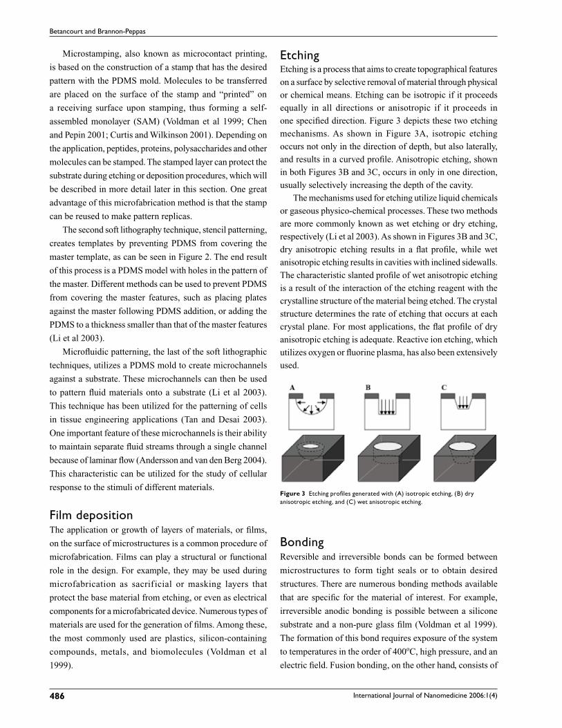
etchingEtching is a process that aims to create topographical features
on a surface by selective removal of material through physical
or chemical means. Etching can be isotropic if it proceeds
equally in all directions or anisotropic if it proceeds in
one specified direction. Figure 3 depicts these two etching
mechanisms. As shown in Figure 3A, isotropic etching
occurs not only in the direction of depth, but also laterally,
and results in a curved profile. Anisotropic etching, shown
in both Figures 3B and 3C, occurs in only in one direction,
usually selectively increasing the depth of the cavity.
The mechanisms used for etching utilize liquid chemicals
or gaseous physico-chemical processes. These two methods
are more commonly known as wet etching or dry etching,
respectively (Li et al 2003). As shown in Figures 3B and 3C,
dry anisotropic etching results in a flat profile, while wet
anisotropic etching results in cavities with inclined sidewalls.
The characteristic slanted profile of wet anisotropic etching
is a result of the interaction of the etching reagent with the
crystalline structure of the material being etched. The crystal
structure determines the rate of etching that occurs at each
crystal plane. For most applications, the flat profile of dry
anisotropic etching is adequate. Reactive ion etching, which
utilizes oxygen or fluorine plasma, has also been extensively
used.
Figure 3 etching profiles generated with (A) isotropic etching, (B) dry anisotropic etching, and (C) wet anisotropic etching.
BondingReversible and irreversible bonds can be formed between
microstructures to form tight seals or to obtain desired
structures. There are numerous bonding methods available
that are specific for the material of interest. For example,
irreversible anodic bonding is possible between a silicone
substrate and a non-pure glass film (Voldman et al 1999).
The formation of this bond requires exposure of the system
to temperatures in the order of 400oC, high pressure, and an
electric field. Fusion bonding, on the other hand, consists of
international Journal of Nanomedicine 2006:1(4) 487
Micro- and nanofabrication in biomedical devices
the annealing of two surfaces at high temperatures (~1000oC)
(Voldman et al 1999).
Bonding of polymers can be carried out through heating
above the glass transition temperature and applying pressure
to seal the structures, through laser welding, or ultrasonic
welding (Becker 2000). In addition, adhesives can also be
utilized to bind two materials. However, the addition of
intermediate layers will affect the properties of the system
and must be taken into account.
Nanofabrication techniquesNanofabrication utilizes principles similar to those of
microfabrication for the generation of patterns or devices at
the nanoscale level, ie, of sizes ranging from 1 to 100 nm.
Some authors consider sizes of up to 1000 nm to be within the
realm of nanostructures. Various microfabrication techniques
have been utilized to achieve features within this range. Soft
lithographic techniques, for example, have been employed
for the production of features with a resolution of less than
200 nm through the use of materials stiffer than PDMS for
the fabrication of the stamp (Chen and Pepin 2001). Features
of less than 40 nm have been produced with conventional
photolithography utilizing light of 193-nm wavelength (Gates
et al 2005). In addition, a number of special lithographic
techniques have been developed to accomplish this
miniaturization and will be discussed in the following sections.
Electron beam lithographyElectron beam lithography is the principal nanofabrication
technique used to create features at the nanoscale level on a
material. This technique utilizes an electron beam to scan a
material and form the desired pattern. Magnetic lenses are
used to focus the beam. Commonly used electron sources are
thermoionic emitters and thermal field emitters which have
outputs in the range of 1 to 200 keV, but are most commonly
used in the range of 50–100 keV (Chen and Pepin 2001). The
resolution obtained through this type of lithography is greatly
influenced by the beam spot size. Specimen position and
beam characteristics are electronically controlled to achieve
the desired nanoscale resolution. Various researchers have
demonstrated resolutions on the order of less than 10 nm.
Chen et al (1996) demonstrated the feasibility of producing 5
to 7 nm-wide etched lines on a silicon substrate by patterning
a polymethylmethacrylate photoresist with an electron
beam of less than 5 nm in diameter at a voltage of 80 kV
(Chen and Ahmed 1993). The main drawback of electron
beam lithography is the cost associated with purchase and
maintenance of the system (Gates et al 2005).
Focused ion beam lithographyThis type of lithographic technique utilizes ions in place
of electrons to pattern a resist. Ions are generated from a
liquid metallic tip, containing elements such as gallium,
“filtered” to allow only one type of ion to interact with the
resist, and focused on the material surface with electrostatic
lenses (Chen and Pepin 2001). Common operational energy
levels are in the range of 10 to 200 keV. Focused ion beam
lithography can also be used to pattern features directly to
a substrate – without the need for a photomask – by either
selective material removal or deposition (Gates et al 2005).
Compared with electron ion beam lithography, the patterning
speed offered by this technique is significantly slower because
of lower achievable ion current density, when compared
with that of electrons. Common feature resolutions are in
the range of 20 nm, with a minimal 5 nm lateral feature size
(Gates et al 2005).
Colloid monolayer lithographyThis lithographic method utilizes self-organized one- or two-
dimensional colloidal systems as layers for nanofabrication.
This technique is an economical alternative to the common
electron or ionic lithographic methods, but is still able to
produce patterns at the nanoscale. Colloidal monolayers can
be generated through a number of self-assembly processes.
For example, colloidal particles can be deposited on the
surface of a substrate in solution prior to solvent evaporation,
through spin coating, or through electrophoresis (Burmeister
et al 1999).
If the size and geometry of the colloidal particles is
precisely controlled, it is in theory possible to also control
the spatial distribution of the colloids. For example,
monodispersed spherical particles can be close-packed
into hexagonally arranged monolayers, ie the conformation
of highest density for this geometry (Burmeister et al
1999). Nonetheless, a number of parameters including
colloid concentration, solvent evaporation rate, wetting
characteristics of the substrate, and competition with
multiple-layer formation influence the resulting array. It
has been reported that the achievable resolution offered by
this technique, when the colloidal monolayer is utilized as a
resist, can be as low as 5 nm in all three dimensions (Curtis
and Wilkinson 2001).
These colloid monolayers can be used as a protective
barrier against etching and, consequently, transfer their semi-
random distribution pattern to the substrate material (Curtis
and Wilkinson 2001). More specifically, these etch masks
would result in the removal of the substrate material located
international Journal of Nanomedicine 2006:1(4)488
Betancourt and Brannon-Peppas
below the colloid interstices. The same analogy can be made
for applications in selective film deposition. Depending on
the application, the colloidal particles can be either removed
or left in place.
Another application of colloidal monolayers has been
recently reported by the group of Dr. Saochen Chen at the
University of Texas at Austin. In their design, colloidal
silica spheres were deposited on the surface of a poly(ε-
caprolactone) film. After self-arrangement of the spheres, a
laser beam was used to irradiate the samples. The spheres,
which have diameters larger than the wavelength of the
light, act as lenses, thus intensifying the effect of the laser
beam on the substrate material (Lu and Chen 2004). Upon
disappearance of the spheres due to laser action, holes
arranged in the original sphere pattern are left behind. Thus,
this technique can be used for high throughput patterning
of nanoholes.
Molecular self assemblyMolecular self assembly is an alternative to lithographic
techniques for the fabrication of features and structures at the
nanometer scale. It is based on thermodynamically favored
interactions of molecules such as peptides, proteins, and
DNA, and other organic or inorganic molecules (Rajagopal
and Schneider 2004). Molecules are spontaneously brought
together to energetically stable conformations favored by
noncovalent forces including hydrophobic, van der Waals,
and electrostatic interactions, as well as hydrogen bonding.
This technique has a number of advantages including the
ability to fabricate three-dimensional structures and the
potential for molecular control of the material (Rajadopal
and Schneider 2004). Molecular self assembly is able to
control pattern formation to the sub-nanometer scale. Self
assembly of monolayers of amphiphilic peptide β-hairpins
was shown to result in organized structures containing
2.5 nm hairpins spaced by less than 0.3 nm (Rajagopal and
Schneider 2004).
Layer-by-layer assembly, one of the self assembly
methods, is based on the consecutive deposition of multiple
thin polyion films from solution utilizing the electrostatic
attraction that develops between oppositely charged
molecules as a driving force for assembly (Decher 1997).
Time for adsorption of polyions onto surfaces ranges from
minutes to hours depending on factors such as polyion type
and concentration. Intermediate washes between sequential
depositions are performed to avoid contamination from
previous solutions. This technique has been widely accepted
because it permits the use of numerous materials, including
biomolecules such as proteins (Decher 1997; Lvov et al 1998)
and DNA (Taton et al 2000). This technique also provides
great control over the film structure, thickness, and function.
In addition, because film formation occurs by adsorption
of polyanions or polycations from solution, the number of
possible morphologies and sizes are only limited by those
of the substrate to be coated.
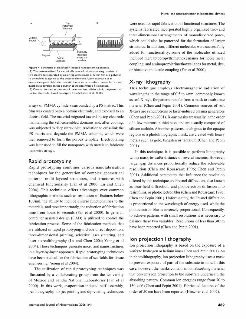
electrically induced nanopatterningElectrically induced nanopatterning techniques utilize
electrostatic interactions between a thin dielectric material
liquid film and an electric field gradient to produce lateral
patterns and structures at the nanometer scale (Schäffer et al
2000). The nanofabrication system is analogous to a capacitor
because it consists of two parallel electrodes separated by an
air gap of less than a micron, as shown in Figure 4. A polymer,
such as polystyrene, is applied to one of the electrodes by spin
coating. Upon exposure to high temperature (above the glass
transition temperature of the polymer) and to an electric field
generated by the voltage across the electrodes, electrostatic
forces develop and result in the destabilization of the
polymeric film. Since the instabilities have a defined periodic
undulation pattern, this system ultimately results in the
formation of polymeric columns at the location of the peaks
of the polymer “wave”, ie, those locations with the highest
polymer thickness or smallest air gap between the polymer
and the top electrode (Schäffer et al 2000, Liu et al 2003).
Lateral column density and order can be altered by changing
parameters such as the initial polymer film thickness, or the
inter-electrode spacing (Schäffer et al 2000).
If in addition the electrode opposite to the polymer
possesses microstructured patterns, the instabilities will
first develop at the locations where the distance between the
electrodes is minimal because of the increased electrostatic
driving force. The result of these instabilities is that the
polymer extends across the air gap toward the opposite
electrode, thus generating nanometer scale “columns” in the
specific pattern of the top electrode (Schäffer et al 2000), as
can be seen in Figure 4. These columns are then solidified
by cooling below the polymer’s glass transition temperature.
Pattern reproductions with features of 140 nm were reported,
but the authors suggest that generation of features of less
than 100 nm is feasible.
This technique has further been utilized to generate
porous templates for the fabrication of nanowire arrays with
very high densities (Thurn-Albrecht et al 2000). This system
utilized a film of the diblock copolymer of polystyrene (PS)
and polymethylmethacrylate (PMMA) that self-assemble into
international Journal of Nanomedicine 2006:1(4) 489
Micro- and nanofabrication in biomedical devices
arrays of PMMA cylinders surrounded by a PS matrix. This
film was coated onto a bottom electrode, and exposed to an
electric field. The material migrated toward the top electrode
maintaining the self-assembled domains and, after cooling,
was subjected to deep ultraviolet irradiation to crosslink the
PS matrix and degrade the PMMA columns, which were
then removed to form the porous template. Electroplating
was later used to fill the nanopores with metals to fabricate
nanowire arrays.
rapid prototypingRapid prototyping combines various nanofabrication
techniques for the generation of complex geometrical
patterns, multi-layered structures, and structures with
chemical functionality (Fan et al 2000; Lu and Chen
2004). This technique offers advantages over common
lithographic methods such as resolution of features below
100 nm, the ability to include diverse functionalities to the
materials, and most importantly, the reduction of fabrication
time from hours to seconds (Fan et al 2000). In general,
computer assisted design (CAD) is utilized to control the
fabrication process. Some of the fabrication methods that
are utilized in rapid prototyping include direct deposition,
three-dimensional printing, selective laser sintering, and
laser stereolithography (Lu and Chen 2004; Yeong et al
2004). These techniques generate micro and nanostructures
in a layer-by-layer approach. Rapid prototyping techniques
have been studied for the fabrication of scaffolds for tissue
engineering (Yeong et al 2004).
The utilization of rapid prototyping techniques was
illustrated by a collaborating group from the University
of Mexico and Sandia National Laboratories (Fan et al
2000). In this work, evaporation-induced self assembly,
pen lithography, ink-jet printing and dip-coating techniques
were used for rapid fabrication of functional structures. The
systems fabricated incorporated highly organized two- and
three-dimensional arrangements of monodispersed pores,
which could also be patterned for the formation of larger
structures. In addition, different molecules were successfully
added for functionality; some of the molecules utilized
included mercaptopropyltrimethoxysilanes for noble metal
coupling, and aminopropyltrimethoxysilanes for metal, dye,
or bioactive molecule coupling (Fan et al 2000).
X-ray lithographyThis technique employs electromagnetic radiation of
wavelengths in the range of 0.5 to 4 nm, commonly known
as soft X-rays, for pattern transfer from a mask to a substrate
material (Chen and Pepin 2001). Common sources of soft
X-rays are synchrotrons or laser-induced plasma generators
(Chen and Pepin 2001). X-ray masks are usually in the order
of a few microns in thickness, and are usually composed of
silicon carbide. Absorber patterns, analogous to the opaque
regions of a photolithographic mask, are created with heavy
metals such as gold, tungsten or tantalum (Chen and Pepin
2001).
In this technique, it is possible to perform lithography
with a mask-to-wafer distance of several microns. However,
larger gap distances proportionally reduce the achievable
resolution (Chen and Rousseaux 1996; Chen and Pepin
2001). Additional parameters that influence the resolution
offered by this technique are Fresnel diffraction, also known
as near-field diffraction, and photoelectron diffusion into
resist films, or photoelectron blur (Chen and Rousseaux 1996;
Chen and Pepin 2001). Unfortunately, the Fresnel diffraction
is proportional to the wavelength of energy used, while the
photoelectron blur is inversely proportional. Consequently,
to achieve patterns with small resolutions it is necessary to
balance these two variables. Resolutions of less than 30 nm
have been reported (Chen and Pepin 2001).
ion projection lithographyIon projection lithography is based on the exposure of a
wafer to hydrogen or helium ions (Chen and Pepin 2001). As
in photolithography, ion projection lithography uses a mask
to prevent exposure of part of the substrate to ions. In this
case, however, the masks contain an ion absorbing material
that prevents ion projection to the substrate underneath the
absorbing pattern. Common ion energies range from 70 to
150 keV (Chen and Pepin 2001). Fabricated features of the
order of 50 nm have been reported (Hirscher et al 2002).
Figure 4 Schematic of electrically-induced nanopatterning process. (A) The system utilized for electrically induced micropatterning consists of two electrodes separated by an air gap of thickness δ. A thin film of a polymer to be molded is applied to the bottom electrode. Upon exposure of an external magnetic field, electrostatic forces surpass surface tension forces, and instabilities develop on the polymer at the sites where δ is smallest. (B) Columns formed at the sites of the major instabilities mimic the pattern of the top electrode. Based on a figure from Schäffer et al (2000).
B
VoltageSource
BottomElectrode
Top PatternedElectrode
Polymer Instabilitydevelops where is smallest
A
V
international Journal of Nanomedicine 2006:1(4)490
Betancourt and Brannon-Peppas
ApplicationsMicro- and nanofabrication techniques have enabled the
scientific and medical community to expand the applications
of already-existing devices through miniaturization, and to
create completely new devices with use of the increased
control of size, morphology, topology, and functionality
offered by these techniques. These novel micro- and
nanodevices have been able to contribute immensely to the
fields of cell biology, molecular biotechnology, and medicine.
It is now possible to study the interactions of biomaterials
with biological systems at the cellular and molecular scale,
and to design new synthetic systems that are able to alter
physiological responses by capitalizing on these findings.
Applications of micro and nanodevices in the medical and
pharmaceutical field are the focus of this section.
Drug delivery devicesMicro- and nanofabrication techniques offer a range of
possibilities for the preparation of peptide, protein, drug,
or gene delivery devices. The ability to control the size,
architecture, topography, and functionality of drug delivery
vehicles could result in the fabrication of systems that behave
in highly predictable manner both in vitro and in vivo, thus
surpassing the capabilities of current drug delivery systems.
injectable micro- and nanodevicesThe fabrication of injectable self-assembled micro reservoirs
for controlled drug delivery was recently reported (Pizzi et
al 2004). The design of these micro reservoirs consists of
metallic cylindrical containers within which the drug was
loaded. The metallic cylinders, made of biocompatible metals
such as titanium or gold, were capped with degradable or
non-degradable temperature sensitive polymeric membranes
on both ends. These membranes could either degrade or
become more permeable at high temperatures. Drug release
could then be controlled externally through the application of
electromagnetic radiation at the site of pathology. Therapeutic
effect was a result of the synergistic combination of drug
delivery at the site of pathology, and heating of the metallic
walls of the micro reservoirs above viable temperatures upon
application of the electromagnetic radiation. Microfabrication
of this system is achieved through deposition of two metal
layers onto a flat silicon substrate and sacrificial layer by
thermal evaporation deposition. Drugs are immobilized onto
the exposed metallic surface either chemically or physically.
Photolithography and wet etching techniques are then
employed to form a large number of independent squared
elements. Upon etching of the sacrificial layer between the
silicon substrate and the metal layers, the internal stress on the
metal causes it to roll into cylindrical configuration. Cylinders
as small as 1.5 microns in diameter and 5 microns in length,
with walls of tens of nm in thickness were reported.
Multilayered nanoparticles prepared by atom-by-atom
or layer-by-layer self assembly for the delivery of drugs or
genes have been developed (Prow et al 2004). These systems
offer the possibility to combine multiple sequential functional
layers that guide the particles through the drug delivery
process one layer at a time. For example, sequential layers
can be loaded with targeting molecules, membrane entrance
molecules, intracellular targeting molecules, and active
agents such as drugs and genes for targeted intracellular
delivery (Prow et al 2004).
Gene delivery with micro and nano-machined devicesA number of micro and nanodevices have been used for the
delivery of genes to target cells. One such system utilizes
“micromechanical piercing” or microprobe elements
to deliver genes coated onto their surface through cell
penetration (Reed et al 1998). Microprobes of 80 microns in
height and with a sharp point of less than 200 nm in diameter
were reported. Successful expression of genes delivered
with microprobes was demonstrated in plant, animal, and
mammalian cells (Reed et al 1998; Hashmi et al 1995). This
system as described is only practical as a research tool for
the transfection of cell monolayers; however, application
of the concept for in vivo therapeutic purposes is being
investigated.
Stents for drug deliveryReed and colleagues developed microfabricated intravascular
stents for the treatment of restenosis (Reed et al 1998). The
design is targeted at increasing the efficacy of pharmaceutical
prevention of restenosis in comparison to local administration
regimes that are unable to cross the internal elastic lamina
and compressed plaque that are present in pathological
vessels. These stents incorporate microprobes, which upon
catheter-based localized deployment are able to perforate
compressed plaque and internal elastic lamina, and deliver
anti-restenosis agents or therapeutic genes, which are
previously coated onto the microprobe surfaces, directly into
coronary tissue. Fabrication of microprobe arrays for ex vivo
study of barrier penetration in rabbit models was carried out
through oxidation, photolithography and anisotropic etching
of a silicon substrate (Reed et al 1998), techniques that result
in planar structures. In order for this system to be feasible for
international Journal of Nanomedicine 2006:1(4) 491
Micro- and nanofabrication in biomedical devices
in vivo applications, the microprobe-containing stents require
cylindrical geometry and the ability for deformation during
balloon-based inflation (Reed et al 1998). The authors discuss
the use novel anodic oxide microfabrication to prepare
structures with high aspect ratio which could be used to solve
some of these problems (Reed et al 1998).
Microneedles for transdermal drug deliveryMicroneedles have been developed for transdermal
administration of proteins, drugs or genes with therapeutic
purposes. Transdermal administration of active agents
offers advantages when compared to intravenous or oral
delivery routes. Intravenous administration is associated
with low patient compliance because of pain caused by
the injection. Oral drug delivery, on the other hand, is
hindered by the degradation of the active agent in the gastro-
intestinal track, low bioavailability because of the difficulties
associated with intestinal absorption, and the sequestration
of much of the drug upon absorption by the liver because
of the first pass effect (Lee and Yamamoto 1989). These
problems are most important when the active agent is a
biomolecule such as a protein or DNA. Current transdermal
delivery systems, however, achieve low bioavailability
because of the low permeability of the stratum corneum,
a layer of dead cells of 10–15 μm in thickness that acts
as a barrier. Numerous chemical and physical methods
have been attempted with the purpose of increasing skin
permeability for drug delivery purposes, including chemical
enhancers, iontophoresis, electroporation, and ultrasound
permeabilization (Bommannan et al 1992; Fang et al 1998;
Lombry et al 2000; Pillai and Panchagnula 2003; Kalia et
al 2004). Microneedles offer an alternative to conventional
transdermal delivery and to permeabilization techniques
because they act as channels that transport the drug across
the stratum corneum barrier into the deeper tissue (dermis)
where it can enter the systemic circulation. In addition,
by careful control of the microneedle mechanical strength
and length, it is possible to deliver drugs across the dermal
barrier while evading the nerves, thus resulting in painless
administration (Henry et al 1998; Kaushik et al 2001; Tao
and Desai 2003).
Microneedles have been fabricated out of a range of
materials including silicon, metals, polymers, and glass
(McAllister et al 2003). Reactive ion etching has been
widely used for the production of solid and hollow silicon
microneedles (Henry et al 1998; McAllister et al 2003).
Here, solid silicon microneedle arrays were produced
by exposing a substrate covered by a chromium mask
patterned into dots of fluorine and oxygen plasma to etch
the uncovered surfaces in such a way that microneedles
are formed on the regions protected by the mask (Henry
et al 1998). Hollow silicon microneedles are prepared by
first etching a silicon substrate to form holes or conduits,
followed by the previously described procedure to form the
microneedle body (McAllister et al 2003). Micromolding
techniques, in conjunction with electrodeposition or micro-
injection molding have been used for the fabrication of
metal or polymer microneedles, respectively (McAllister
et al 2003). Microneedles with various tip geometries were
also reported.
As a proof-of-concept study, solid silicon microneedles
of 150 μm in height and less than 1 μm in tip radius of
curvature were tested on human epidermis ex vivo. Results
showed that microneedle arrays produced by this method
could be easily inserted, removed, and reinserted from
the skin without significant damage, and resulted in up to
25 000-fold increase in permeability of calcein as a model
drug (Henry et al 1998). Later ex vivo studies on human
epidermis showed that the permeability to calcein, insulin,
bovine serum albumin, and even polystyrene microspheres of
50 μm diameter was increased by more than one or two orders
of magnitude when solid microneedles were either inserted,
or inserted and removed, respectively (McAllister et al 2003).
In vitro studies on DU145 cells showed cells could uptake
calcein administered with solid microneedles with only about
10% cell mortality (McAllister et al 2003). Finally, in vivo
studies of transdermal delivery with hollow microneedles in
diabetic hairless rats showed that microinjection of insulin
resulted in a statistically significant reduction of the blood
sugar level for a period of 5 hours. In addition, in vivo use
of solid microneedle arrays on human volunteers suggested
that application was not painful and did not cause irritation
(Henry et al 1998).
Different microneedle designs have been utilized by other
groups for the delivery of the antisense oligonucleotides
(Lin et al 2001), proteins (Matriano et al 2002), and plasmid
DNA (Mikszta et al 2002; Chabri et al 2004). The fabrication
of biodegradable microneedles has also been proposed
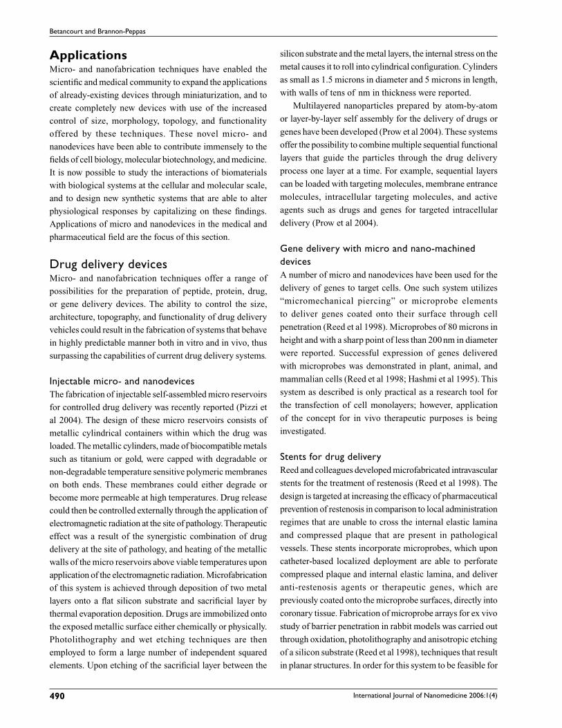
(Park et al 2005). Figure 5 shows examples of solid silicon
microneedles fabricated by reactive ion etching.
Recently, emphasis has been placed on the fabrication
and utilization of devices for enhanced microneedle drug
delivery. For example, Zahn and colleagues have developed
an on-chip planar positive displacement pump for portable
continuous drug delivery with microfabrication techniques
(Zahn et al 2004).
international Journal of Nanomedicine 2006:1(4)492
Betancourt and Brannon-Peppas
implantable microfabricated drug delivery chipsImplantable microchips have been developed for on-demand
pulsatile release of a number of different drugs in varied
doses by the Langer group (Santini et al 1999; Langer and
Peppas 2003). The design consists of the microfabrication
of reservoirs within silicon substrates in which the drug is
immobilized in either liquid or solid form (Santini et al 1999).
These reservoirs are covered by a membrane of a material that
can dissolve upon exposure to an electrochemical stimulus,
such as gold. The microchip contains a cathode made of
silicon nitride or silicon dioxide (Santini et al 1999). An
electrical potential can be established between this cathode
and one of the reservoir membranes which act as anodes. This
potential triggers dissolution of the membrane, and results
in the pulsatile release of the drug.
The implantable microreservoirs were generated by
sequential microfabrication techniques including UV
photolithography, chemical vapor deposition, electron beam
evaporation and reactive ion etching (Santini et al 1999).
The model microchips had a size of 17 mm on each side,
and contained approximately 1000 reservoirs, each of which
could contain a volume of up to 25 nL (Santini et al 1999).
More recently, a biodegradable microchip system
fabricated from poly(lactic-co-glycolic acid)-based polymers
was developed for long term pulsatile delivery of drugs
(Richards et al 2003). Specifically, the main body of the
device which contains reservoirs for drugs was made from
poly(L-lactic acid) (PLLA), while the membranes covering
these reservoirs were prepared from the fast-degrading
polymer poly(D,L-lactic-co-glycolic acid) (PLGA).
Using PLGA of different molecular weight for membrane
preparation, they were able to show release of dextran,
heparin, and human growth hormone at different time
intervals. Fabrication of these implantable devices utilized
compression-molding for generation of the reservoirs on a
PLLA disk, and microinjection for generation of reservoir
membranes and drug filling (Richards et al 2003). Each 11-
mm device had 36 reservoirs with a capacity of more than
120 nL each.
Low and colleagues have also developed responsive,
reversible polymeric valves based on hydrogel actuators for
microchip delivery of drugs in response to physiological
changes (Low et al 2000). Such system would deliver active
agents only when needed, thus avoiding unnecessary or
possibly hazardous release of drugs which could occur from
‘pre-programmed” microchips, such as those described
above.
Microfabricated bio- and muco-adhesive systemsVarious alternative techniques have been investigated for
improved oral delivery of drugs and biomolecules which
currently offers only limited bioavailability as a result of
the properties of the gastro intestinal track: low stomach
pH and presence of proteases that degrade active agents,
and poor intestinal absorption of macromolecules. Bio- and
muco-adhesive systems offer the possibility to increase
the residence time of drugs or drug carriers at the site
of absorption, thus increasing the possibility that these
drugs are able to enter the systemic circulation and exert
a therapeutic effect. Micro- and nanofabrication offer
the opportunity to design and produce oral drug delivery
systems with high degree of functionality for bioadhesive
purposes.
One such system utilizes poly(methacrylate) micro-
particles for bioadhesion. These microparticles were
fabricated by lithography and reactive ion etching (Tao
and Desai 2003), and were surface modified with amine
groups to which biological molecules, such as avidin-lectin
complexes, could be attached. Lectins were chosen because
they are known to bind glycoconjugates on cell surfaces with
great affinity. The microparticle square morphology and size
(150 μm wide by 3 μm in thickness) were chosen in order to
maximize the surface area in contact with the intestinal walls.
This system was found to significantly increase binding to
Caco-2 monolayers.
Other groups have proposed the use of micro- and
nanofabrication techniques for the creation of patterned
mucoadhesive structures based on the interactions between
mucin, ie, the main organic component of intestinal mucus,
and hydrophilic polymers (Kim and Peppas 2003; Peppas
Figure 5 Scanning electron microscopy image of relatively short solid silicon microneedles (25 μm in height) prepared by reactive ion etching. These nanoparticles were designed for cutaneous gene delivery. reproduced with permission from McAllister D, wang P, Davis S, et al. 2003. Microfabricated needles for transdermal delivery of macromolecules and nanoparticles: fabrication methods and transport studies. Proc Natl Acad Sci U S A, 100:13755-60. Copyright © 2003 National Academy of Sciences, U.S.A.
international Journal of Nanomedicine 2006:1(4) 493
Micro- and nanofabrication in biomedical devices
and Huang 2004). Lithographic photopolymerization of
hydrogels onto silicon substrates was proposed for these
systems.
Micro and nanofabricated biosensorsSensors consist of devices that detect and/or measure a
specific compound or condition in their environment, and
generate a corresponding output through the action of a
transducer. Depending on the design, micro- and nanosensors
are able to identify changes in pressure, temperature, ionic
strength, or concentration or a target molecule, just like their
macro-metric counterparts.
Microcantilevers have been shown in the past to work
as very sensitive transducers for sensing applications. Their
function is based on the generation of surface stresses, and a
subsequent bending of the cantilever in response to changes
in environmental conditions, or upon binding of a target
molecule.
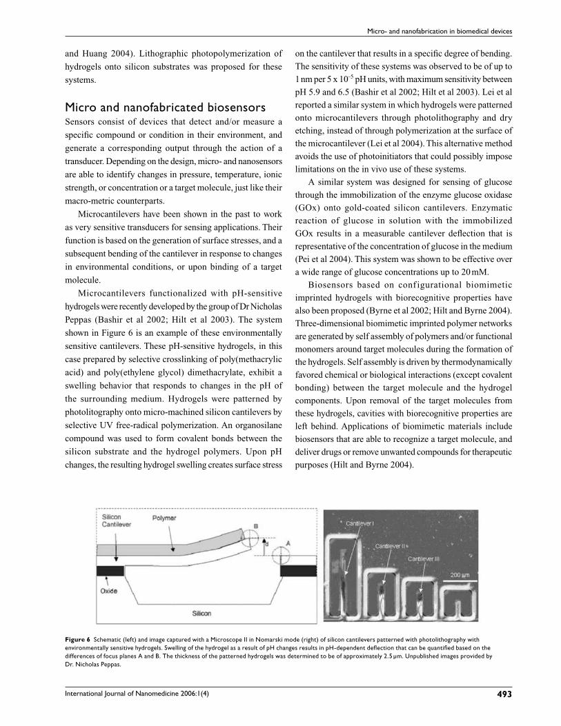
Microcantilevers functionalized with pH-sensitive
hydrogels were recently developed by the group of Dr Nicholas
Peppas (Bashir et al 2002; Hilt et al 2003). The system
shown in Figure 6 is an example of these environmentally
sensitive cantilevers. These pH-sensitive hydrogels, in this
case prepared by selective crosslinking of poly(methacrylic
acid) and poly(ethylene glycol) dimethacrylate, exhibit a
swelling behavior that responds to changes in the pH of
the surrounding medium. Hydrogels were patterned by
photolitography onto micro-machined silicon cantilevers by
selective UV free-radical polymerization. An organosilane
compound was used to form covalent bonds between the
silicon substrate and the hydrogel polymers. Upon pH
changes, the resulting hydrogel swelling creates surface stress
on the cantilever that results in a specific degree of bending.
The sensitivity of these systems was observed to be of up to
1 nm per 5 x 10⁻⁵ pH units, with maximum sensitivity between
pH 5.9 and 6.5 (Bashir et al 2002; Hilt et al 2003). Lei et al
reported a similar system in which hydrogels were patterned
onto microcantilevers through photolithography and dry
etching, instead of through polymerization at the surface of
the microcantilever (Lei et al 2004). This alternative method
avoids the use of photoinitiators that could possibly impose
limitations on the in vivo use of these systems.
A similar system was designed for sensing of glucose
through the immobilization of the enzyme glucose oxidase
(GOx) onto gold-coated silicon cantilevers. Enzymatic
reaction of glucose in solution with the immobilized
GOx results in a measurable cantilever deflection that is
representative of the concentration of glucose in the medium
(Pei et al 2004). This system was shown to be effective over
a wide range of glucose concentrations up to 20 mM.
Biosensors based on conf igurational biomimetic
imprinted hydrogels with biorecognitive properties have
also been proposed (Byrne et al 2002; Hilt and Byrne 2004).
Three-dimensional biomimetic imprinted polymer networks
are generated by self assembly of polymers and/or functional
monomers around target molecules during the formation of
the hydrogels. Self assembly is driven by thermodynamically
favored chemical or biological interactions (except covalent
bonding) between the target molecule and the hydrogel
components. Upon removal of the target molecules from
these hydrogels, cavities with biorecognitive properties are
left behind. Applications of biomimetic materials include
biosensors that are able to recognize a target molecule, and
deliver drugs or remove unwanted compounds for therapeutic
purposes (Hilt and Byrne 2004).
Figure 6 Schematic (left) and image captured with a Microscope ii in Nomarski mode (right) of silicon cantilevers patterned with photolithography with environmentally sensitive hydrogels. Swelling of the hydrogel as a result of pH changes results in pH-dependent deflection that can be quantified based on the differences of focus planes A and B. The thickness of the patterned hydrogels was determined to be of approximately 2.5 μm. Unpublished images provided by Dr. Nicholas Peppas.
international Journal of Nanomedicine 2006:1(4)494
Betancourt and Brannon-Peppas
ConclusionsAdaptation of micro- and nanofabrication techniques derived
from the semiconductor industry has led to the creation of
novel devices for use in the medical and pharmaceutical fields.
These systems promise to offer improved characteristics
including enhanced control of feature geometry, size and
complexity, feasible mass production, portability, and
miniaturization. In addition, because these techniques enable
the production of devices at the cellular and sub-cellular
levels, they open the doors to the creation of new strategies
for the study and manipulation of molecules, cells, and
tissues, thus providing new avenues for the investigation of
pathological mechanisms and novel treatment options. This
paper describes some of the main micro- and nanofabrication
techniques that have been published in the literature and
examples of how these techniques have revolutionized the
fields of drug delivery and diagnostics.
ReferencesAndersson H, van den Berg A. 2004. Microfabrication and microfluidics
for tissue engineering: state of the art and future opportunities. Lab on a Chip, 4:98-103.
Bashir R, Hilt J, Elibol O, et al. 2002. Micromechanical cantilever as an ultrasensitive ph microsensor. Appl Phys Lett, 81:3091-3.
Becker H, Gärtner C. 2000. Polymer microfabrication methods for microfluidic analytical applications. Electrophoresis, 21:12-26.
Blanchette JO, Kavimandan N, Peppas NA. 2004. Principles of transmucosal delivery of therapeutic agents. Biomed Pharmacother, 58:142-51.
Bommannan D, Okuyama H, Stauffer P, et al. 1992. Sonophoresis. I. The use of high-frequency ultrasound to enhance transdermal drug delivery. Pharm Res, 9:559-64.
Brannon-Peppas L, Blanchette JO. 2004. Nanoparticle and targeted systems for cancer therapy. Adv Drug Deliv Rev, 56:1649-59.
Burmeister F, Badowsky W, Braun T, et al. 1999. Colloid monolayer lithography-a flexible approach for nanostructuring of surfaces. Applied Surface Science, 144-155:461-6.
Byrne ME, Oral E, Hilt JZ, et al. 2002. Networks for recognition of biomolecules: molecular imprinting and micropatterning poly(ethylene glycol)-containing films. Polymers for Advanced Technologies, 13:798-816.
Chabri F, Bouris K, Jones T, et al. 2004. Microfabricated silicon microneedles for nonviral cutaneous gene delivery. Br J Dermatol, 150:869-77.
Chen W, Ahmed H. 1993. Fabrication of 5-7 nm wide etched lines in silicon using 100 kev electron-beam lithography and polymethylmethacrylate resist. Appl Phys Lett, 62:1499-501.
Chen Y, Pepin A. 2001. Nanofabrication: conventional and nonconventional methods. Electrophoresis, 22:187-207.
Chen Y, Rousseaux F, Haghiri-Gosnet A, et al. 1996. Proximity X-ray lithography as a quick replication technique in nanofabrication : recent progress and perspectives. Microelectronic Engineering, 30:191-4.
Curtis A, Wilkinson C. 2001. Nanotechniques and approaches in biotechnology. Trends Biotechnol, 19:97-101.
Decher G. 1997. Fuzzy nanoassemblies: toward layered polymeric multicomposites. Science, 277:1232-7.
Fan H, Lu Y, Stump A, et al. 2000. Rapid prototyping of patterned functional structures. Nature, 405:56-60.
Fang JY, Lin HH, Chen HI, et al. 1998. Development and evaluation on transdermal delivery of enoxacin via chemical enhancers and physical iontophoresis. J Control Release, 54:293-304.
Gates BD, Xu Q, Stewart M, et al. 2005. New approaches to nanofabrication: molding, printing and other techniques. Chem Rev, 105:1171-96.
Hashmi S, Ling P, Hashmi G, et al. 1995. Genetic transformation of nematodes using arrays of micromechanical piercing structures. Biotechniques, 19:766-70.
Henry S, McAllister DV, Allen MG, et al. 1998. Microfabricated microneedles: a novel approach to transdermal drug delivery. J Pharm Sci, 87:922-5.
Hilt J, Gupta A, Bashir R, et al. 2003. Ultrasensitive biomems sensors based on microcantilevers patterned with environmentally responsive hydrogels. Biomed Microdevices, 5:177-84.
Hilt JZ, Byrne ME. 2004. Configurational biomimesis in drug delivery: molecular imprinting of biologically significant molecules. Adv Drug Del Rev, 56:1599-620.
Hirscher S, Kummel M, Kirch O, et al. 2002. Ion projection lithography below 70 nm: tool performance and resist process. Microelectronic Engineering, 61-62:301-7.
Kalia YN, Naik A, Garrison J, et al. 2004. Iontophoretic drug delivery. Adv Drug Del Rev, 56:619-58.
Kaushik S, Hord AH, Denson DD, et al. 2001. Lack of pain associated with microfabricated microneedles. Anesth Analg, 92:502-4.
Kim B, Peppas NA. 2003. Poly(ethylene glycol)-containing hydrogels for oral protein delivery applications. Biomedical Microdevices, 5:333-41.
Langer R, Peppas NA. 2003. Advances in biomaterials, drug delivery, and bionanotechnology. AIChE J, 49:2990-3006.
Lee VHL, Yamamoto A. 1989. Penetration and enzymatic barriers to peptide and protein absorption. Adv Drug Del Rev, 4:171-207.
Lei M, Gu Y, Baldi A, et al. 2004. High-resolution technique for fabricating environmentally sensitive hydrogel microstructures. Langmuir, 20:8947-51.
Li N, Tourovskaia A, Folch A. 2003. Biology on a chip: microfabrication for studying the behavior of cultured cells. Crit Rev Biomed Eng, 31:423-88.
Lin W, Cormier M, Samiee A, et al. 2001. Transdermal delivery of antisense oligonucleotides with microprojection patch (macroflux) technology. Pharm Res, 18:1789-93.
Liu T, Burger C, Chu B. 2003. Nanofabrication in polymer matrices. Prog Colloid Polym Sci, 28:5-26.
Lombry C, Dujardin N, Préat V. 2000. Transdermal delivery of macromolecules using skin electroporation. Pharm Res, 17:32-7.
Low LM, Seetharaman S, He K-Q, et al. 2000. Microactuators toward microvalves for responsive controlled drug delivery. Sens Actuators B Chem, 67:149-60.
Lu Y, Chen S. 2004. Micro and nano-fabrication of biodegradable polymers for drug delivery. Adv Drug Del Rev, 56:1621-33.
Lvov YM, Lu Z, Schenkman JB, et al. 1998. Direct electrochemistry of myoglobin and cytochrome p450cam in alternate layer-by-layer films with DNA and other polyions. J Am Chem Soc, 120:4073-80.
Matriano JA, Cormier M, Johnson J, et al. 2002. Macroflux microprojection array patch technology: a new and efficient approach for intracutaneous immunization. Pharm Res, 19:63-70.
McAllister D, Wang P, Davis S, et al. 2003. Microfabricated needles for transdermal delivery of macromolecules and nanoparticles: fabrication methods and transport studies. Proc Natl Acad Sci U S A, 100:13755-60.
Mikszta JA, Alarcon JB, Brittingham JM, et al. 2002. Improved genetic immunization via micromechanical disruption of skin-barrier function and targeted epidermal delivery. Nat Med, 8:415-19.
Park JH, Allen MG, Prausnitz MR. 2005. Biodegradable polymer microneedles: fabrication, mechanics and transdermal drug delivery. J Control Rel, 104:51-66.
Pei J, Tian F, Thundat T. 2004. Glucose biosensor based on the micro-cantilever. Anal Chem, 76:292-7.
international Journal of Nanomedicine 2006:1(4) 495
Micro- and nanofabrication in biomedical devices
Peppas NA, Huang Y. 2004. Nanoscale technology of mucoadhesive interactions. Adv Drug Del Rev, 56:1675-87.
Pillai O, Panchagnula R. 2003. Transdermal delivery of insulin from poloxamer gel: ex vivo and in vivo skin permeation studies in rat using iontophoresis and chemical enhancers. J Control Rel, 89:127-40.
Pizzi M, De Martiis O, Grasso V. 2004. Fabrication of self assembled micro reservoirs for controlled drug release. Biomed Microdevices, 6:155-8.
Prow TW, Kotov NA, Lvov YM, et al. 2004. Nanoparticles, molecular biosensors, and multispectral confocal microscopy. Journal of Molecular Histology, 35:555-64.
Rajagopal K, Schneider J. 2004. Self-assembling peptides and proteins for nanotechnological applications. Curr Opin Struct Biol, 14:480-6.
Reed ML, Wu C, Kneller J, et al.1998. Micromechanical devices for intravascular drug delivery. J Pharm Sci, 87:1387-94.
Richards Grayson AC, Choi IS, Tyler BM, et al. 2003. Multi-pulse drug delivery from a resorbable polymeric microchip device. Nat Mat, 2:767-72.
Santini J, Cima M, Langer R. 1999. A controlled-release microchip. Nature, 397:335-8.
Schäffer E, Thurn-Albrecht T, Russell TP, et al. 2000. Electrically induced structure formation and pattern transfer. Nature, 403:874-7.
Seeman NC. 2003. DNA in a material world. Nature, 421:427-31.Tan W, Desai TA. 2003. Microfluidic patterning of cells in extracellular
matrix biopolymers: effects of channel size, cell type, and matrix biopolymers: effects of channel size, cell type, and matrix composition on pattern integrity. Tissue Eng, 9:255-67.
Tao S, Desai T. 2003. Microfabricated drug delivery systems: from particles to pores. Adv Drug Del Rev, 55:315-28.
Taton TA, Mucic RC, Mirkin CA, et al. 2000. The DNA-mediated formation of supramolecular mono- and multilayered nanoparticle structures. J Am Chem Soc, 122:6305-6.
Thurn-Albrecht T, Schotter J, Kästle GA, et al. 2000. Ultrahigh-Density nanowire arrays grown in self-assembled diblock copolymer templates. Science, 290:2126-9.
Voldman J, Gray ML, Schmidt MA. 1999. Microfabrication in biology and medicine. Ann Rev Biomed Eng, 1:401-25.
Xia Y, Whitesides GM. 1998. Soft lithography. Ann Rev Mat Sci, 28:153-84.
Yeong W-Y, Chua C-K, Leong K-F, et al. 2004. Rapid prototyping in tissue engineering: challenges and potential. Trends Biotechnol, 22:643-52.
Yurke B, Mills AP, Blakey MI, et al. 2003. DNA fuel for free-running nanomachines. Phys Rev Lett, 90:118102.
Zahn JD, Deshmukh A, Pisano AP, et al. 2004. Continuous on-chip micropumping for microneedle enhanced drug delivery. Biomed Microdevices, 6:183-90