Embed Size (px)
Citation preview
High-resolution nanofabrication using a highly focused electron beam Thomas Aref, Mikas Remeika, and Alexey Bezryadin Copyright 2008 American Institute of Physics This article may be downloaded for personal use only. Any other use requires prior permission of the author and the American Institute of Physics. The following article appeared in The Journal of Applied Physics 104, 024312 (2008) and may be found at http://link.aip.org/link/?JAPIAU/104/024312/1.
High-resolution nanofabrication using a highly focused electron beamThomas Aref, Mikas Remeika, and Alexey Bezryadina�
Department of Physics, University of Illinois at Urbana-Champaign, 1110 W. Green Street, Urbana, Illinois61801, USA
�Received 10 April 2008; accepted 19 May 2008; published online 24 July 2008�
A highly focused electron beam can be used to shape nanodevices. We demonstrate electron beametching of nanoholes through multiwalled carbon nanotubes �MWNTs� and niobium nanowires.Nanoholes, as small as �2.5 nm in diameter, can be reproducibly fabricated. This technique canalso be used to fabricate constrictions and larger nanoholes in MWNTs. We argue that with someimprovement, this technique might be used to pattern suspended graphene by the removal oftargeted single atoms. © 2008 American Institute of Physics. �DOI: 10.1063/1.2957590�
I. INTRODUCTION
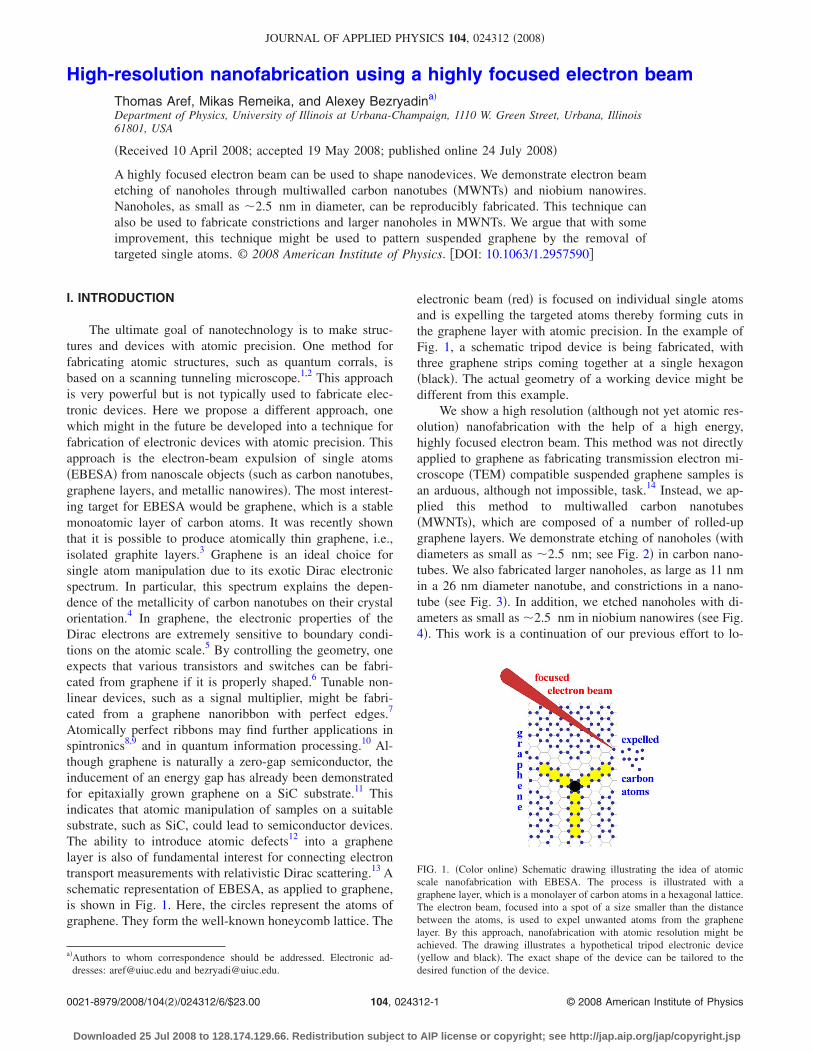
The ultimate goal of nanotechnology is to make struc-tures and devices with atomic precision. One method forfabricating atomic structures, such as quantum corrals, isbased on a scanning tunneling microscope.1,2 This approachis very powerful but is not typically used to fabricate elec-tronic devices. Here we propose a different approach, onewhich might in the future be developed into a technique forfabrication of electronic devices with atomic precision. Thisapproach is the electron-beam expulsion of single atoms�EBESA� from nanoscale objects �such as carbon nanotubes,graphene layers, and metallic nanowires�. The most interest-ing target for EBESA would be graphene, which is a stablemonoatomic layer of carbon atoms. It was recently shownthat it is possible to produce atomically thin graphene, i.e.,isolated graphite layers.3 Graphene is an ideal choice forsingle atom manipulation due to its exotic Dirac electronicspectrum. In particular, this spectrum explains the depen-dence of the metallicity of carbon nanotubes on their crystalorientation.4 In graphene, the electronic properties of theDirac electrons are extremely sensitive to boundary condi-tions on the atomic scale.5 By controlling the geometry, oneexpects that various transistors and switches can be fabri-cated from graphene if it is properly shaped.6 Tunable non-linear devices, such as a signal multiplier, might be fabri-cated from a graphene nanoribbon with perfect edges.7
Atomically perfect ribbons may find further applications inspintronics8,9 and in quantum information processing.10 Al-though graphene is naturally a zero-gap semiconductor, theinducement of an energy gap has already been demonstratedfor epitaxially grown graphene on a SiC substrate.11 Thisindicates that atomic manipulation of samples on a suitablesubstrate, such as SiC, could lead to semiconductor devices.The ability to introduce atomic defects12 into a graphenelayer is also of fundamental interest for connecting electrontransport measurements with relativistic Dirac scattering.13 Aschematic representation of EBESA, as applied to graphene,is shown in Fig. 1. Here, the circles represent the atoms ofgraphene. They form the well-known honeycomb lattice. The
electronic beam �red� is focused on individual single atomsand is expelling the targeted atoms thereby forming cuts inthe graphene layer with atomic precision. In the example ofFig. 1, a schematic tripod device is being fabricated, withthree graphene strips coming together at a single hexagon�black�. The actual geometry of a working device might bedifferent from this example.
We show a high resolution �although not yet atomic res-olution� nanofabrication with the help of a high energy,highly focused electron beam. This method was not directlyapplied to graphene as fabricating transmission electron mi-croscope �TEM� compatible suspended graphene samples isan arduous, although not impossible, task.14 Instead, we ap-plied this method to multiwalled carbon nanotubes�MWNTs�, which are composed of a number of rolled-upgraphene layers. We demonstrate etching of nanoholes �withdiameters as small as �2.5 nm; see Fig. 2� in carbon nano-tubes. We also fabricated larger nanoholes, as large as 11 nmin a 26 nm diameter nanotube, and constrictions in a nano-tube �see Fig. 3�. In addition, we etched nanoholes with di-ameters as small as �2.5 nm in niobium nanowires �see Fig.4�. This work is a continuation of our previous effort to lo-
a�Authors to whom correspondence should be addressed. Electronic ad-dresses: [email protected] and [email protected].
FIG. 1. �Color online� Schematic drawing illustrating the idea of atomicscale nanofabrication with EBESA. The process is illustrated with agraphene layer, which is a monolayer of carbon atoms in a hexagonal lattice.The electron beam, focused into a spot of a size smaller than the distancebetween the atoms, is used to expel unwanted atoms from the graphenelayer. By this approach, nanofabrication with atomic resolution might beachieved. The drawing illustrates a hypothetical tripod electronic device�yellow and black�. The exact shape of the device can be tailored to thedesired function of the device.
JOURNAL OF APPLIED PHYSICS 104, 024312 �2008�
0021-8979/2008/104�2�/024312/6/$23.00 © 2008 American Institute of Physics104, 024312-1
Downloaded 25 Jul 2008 to 128.174.129.66. Redistribution subject to AIP license or copyright; see http://jap.aip.org/jap/copyright.jsp
cally modify nanowires with an electron beam.15 We de-scribe the details of the fabrication and consider possibleapplications of this method.
The level of precision in removal of material with aTEM beam required for EBESA has not yet been achieved.Previously, pores, wires, constrictions, and other structureshave been fabricated with a TEM using a similar method.Direct etching of resists by a focused electron beam has beenexplored.16,17 Nanopores in silicon nitride and silicon oxidemembranes have been fabricated.18,19 Constrictions in nio-bium have also been made.15 Gold nanogaps have also beenfabricated.20 Wires, constrictions, loops, and other structureswere recently reported.21,22 Nanoholes in carbon and variousother materials have also been reported.23 Exposure of car-bon nanotubes to uniform electron beams have been exten-sively investigated and effects such as bonding,24
etching,25–27 and amorphization28 have been seen. Focusedelectron beams have been used to cut bundles of SWNTs.29 Afocused electron beam was also used to etch a single wall ofa MWNT30 and to create dislocations in SWNTs.31 Cuts havebeen etched in boron nitride nanotubes as well.32
II. EXPERIMENT
We etched nanoholes in both MWNTs deposited directlyon TEM compatible �i.e., transparent to the electron beam�
membranes and MWNTs suspended across slits. We usedlow stress silicon nitride membranes �SPI Supplies, Inc.�which were 100�100 �m2 and 100 nm thick. The siliconframe supporting the membrane was 3�3 mm2 and200 �m thick to fit into a standard TEM holder or a hotstage. Using potassium hydroxide �KOH� etching, we alsofabricated our own 50 nm thick membranes in a 5�8 mm2 and 400 microns thick silicon frame. We built acustom TEM holder to accommodate our membranes. Arcdischarge MWNTs �Alfa Aesar� were deposited by crushingthe soot powder containing the MWNTs between two piecesof polydimethylsiloxane �PDMS� �Sylgard 184, Dow Corn-ing�, thus dispersing the nanotubes. Touching and removingthe nanotube covered PDMS to the membrane or slit trans-ferred nanotubes to the sample.33 This ensured that the nano-tubes were only on one side of the membrane facing awayfrom the TEM beam when the sample was inserted into theTEM. Because the silicon nitride is electron transparent, thenanotube is visible �see Fig. 5�. The main disadvantage ofplacing the nanotube directly on the silicon nitride is the lossof detail from the amorphous silicon nitride obscuring thenanotube.
Suspending nanotubes across an open slit in a substrateimproves the resolution of the TEM images �see Fig. 2 or 3�.200 nm−1 �m wide slits were formed by making cuts with
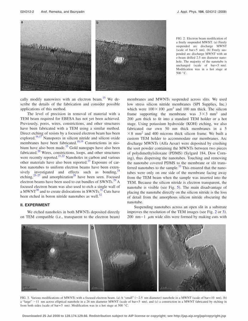
FIG. 2. Electron beam modification ofa freely suspended MWNT. �a� Freelysuspended arc discharge MWNT�scale of bar=5 nm�. �b� Freely sus-pended arc discharge MWNT with ane-beam drilled 2.5 nm diameter nano-hole. The majority of the nanotube isunchanged �scale of bar=5 nm�.Modification was in a hot stage at500 °C.
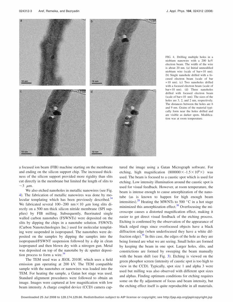
FIG. 3. Various modifications of MWNTs with a focused electron beam. �a� A “small” ��2.5 nm diameter� nanohole in a MWNT �scale of bar=10 nm�, �b�a “large” �11 nm across elliptical nanohole in a 26 nm diameter MWNT �scale of bar=5 nm�, and �c� a constriction in a MWNT fabricated by etching infrom both sides �scale of bar=5 nm�. Modification was in a hot stage at 500 °C.
024312-2 Aref, Remeika, and Bezryadin J. Appl. Phys. 104, 024312 �2008�
Downloaded 25 Jul 2008 to 128.174.129.66. Redistribution subject to AIP license or copyright; see http://jap.aip.org/jap/copyright.jsp
a focused ion beam �FIB� machine starting on the membraneand ending on the silicon support chip. The increased thick-ness of the silicon support provided more rigidity than slitscut directly in the membrane but limited the length of slits to�3 �m.
We also etched nanoholes in metallic nanowires �see Fig.4�. The fabrication of metallic nanowires was done by mo-lecular templating which has been previously described.34
We fabricated several 100–200 nm�10 �m long slits di-rectly on a 500 nm thick silicon nitride membrane �SPI sup-plies� by FIB milling. Subsequently, fluorinated singlewalled carbon nanotubes �FSWNTs� were deposited on theslits by dipping the chips in a nanotube solution. FSWNTs�Carbon Nanotechnologies Inc.� used for molecular templat-ing were suspended in isopropanol. The nanotubes were de-posited on the samples by dipping the samples into theisopropanol/FSWNT suspension followed by a dip in cleanisopropanol and then blown dry with a nitrogen gun. Metalwas deposited on top of the nanotube by dc sputter deposi-tion process to form a wire.34
The TEM used was a JEOL 2010F, which uses a fieldemission gun operating at 200 kV. The TEM compatiblesample with the nanotubes or nanowires was loaded into theTEM. For heating the sample, a Gatan hot stage was used.Standard alignment procedures were followed to obtain animage. Images were captured at low magnification with lowbeam intensity. A charge coupled device �CCD� camera cap-
tured the image using a Gatan Micrograph software. Foretching, high magnification �800000� -1.5�106�� wasused. The beam is focused to a caustic spot which is used foretching. Low intensity illumination around the caustic spot isused for visual feedback. However, at room temperature, thebeam is intense enough to cause amorphization of the nano-tube �as is known to happen for high enough beamintensities�.28 Heating the MWNTs to 500 °C in a hot stageminimized this amorphization effect.30 Overfocusing the mi-croscope causes a distorted magnification effect, making iteasier to get direct visual feedback of the etching process.Etching is confirmed by the observation of the appearance ofblack edged rings since overfocused objects have a blackdiffraction edge �when underfocused they have a white dif-fraction edge�.35 In this case, the edges of the hole as they arebeing formed are what we are seeing. Small holes are formedby keeping the beam in one spot. Larger holes, slits, andconstrictions are formed by sweeping the beam manuallywith the beam shift �see Fig. 3�. Etching is viewed on thegreen phosphor screen �intensity of caustic spot is too high toview in the CCD�. Typically, spot size 1 and alpha 3 wereused but milling was also observed with different spot sizesand alphas. Finding optimum conditions for etching requiressome on the fly adjustment of focus and beam intensity, butthe etching effect itself is quite reproducible in all materials.
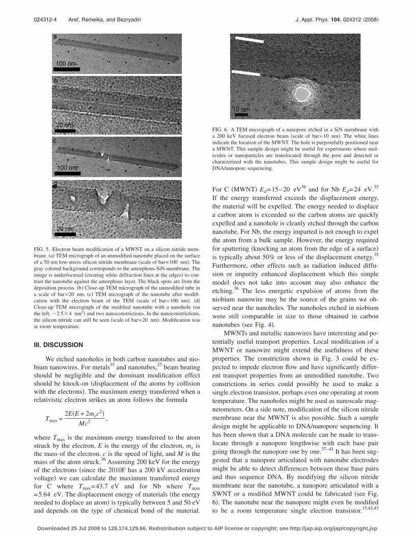
FIG. 4. Drilling multiple holes in aniobium nanowire with a 200 keVelectron beam. The width of the wireis about 20 nm. �a� Initial unmodifiedniobium wire �scale of bar=10 nm�.�b� Single nanohole drilled with a fo-cused electron beam �scale of bar=10 nm�. �c� Two nanoholes drilledwith a focused electron beam �scale ofbar=10 nm�. �d� Three nanoholesdrilled with focused electron beam�scale of bar=10 nm�. The sizes of theholes are 3, 2, and 2 nm, respectively.The distances between the holes are 6and 9 nm. Grains of the material typi-cally form near the holes drilled andare visible as darker spots. Modifica-tion was at room temperature.
024312-3 Aref, Remeika, and Bezryadin J. Appl. Phys. 104, 024312 �2008�
Downloaded 25 Jul 2008 to 128.174.129.66. Redistribution subject to AIP license or copyright; see http://jap.aip.org/jap/copyright.jsp
III. DISCUSSION
We etched nanoholes in both carbon nanotubes and nio-bium nanowires. For metals35 and nanotubes,27 beam heatingshould be negligible and the dominant modification effectshould be knock-on �displacement of the atoms by collisionwith the electrons�. The maximum energy transferred when arelativistic electron strikes an atom follows the formula
Tmax =2E�E + 2mec
2�Mc2 ,
where Tmax is the maximum energy transferred to the atomstruck by the electron, E is the energy of the electron, me isthe mass of the electron, c is the speed of light, and M is themass of the atom struck.36 Assuming 200 keV for the energyof the electrons �since the 2010F has a 200 kV accelerationvoltage� we can calculate the maximum transferred energyfor C where Tmax=43.7 eV and for Nb where Tmax
=5.64 eV. The displacement energy of materials �the energyneeded to displace an atom� is typically between 5 and 50 eVand depends on the type of chemical bond of the material.
For C �MWNT� Ed=15–20 eV36 and for Nb Ed=24 eV.35
If the energy transferred exceeds the displacement energy,the material will be expelled. The energy needed to displacea carbon atom is exceeded so the carbon atoms are quicklyexpelled and a nanohole is cleanly etched through the carbonnanotube. For Nb, the energy imparted is not enough to expelthe atom from a bulk sample. However, the energy requiredfor sputtering �knocking an atom from the edge of a surface�is typically about 50% or less of the displacement energy.35
Furthermore, other effects such as radiation induced diffu-sion or impurity enhanced displacement which this simplemodel does not take into account may also enhance theetching.36 The less energetic expulsion of atoms from theniobium nanowire may be the source of the grains we ob-served near the nanoholes. The nanoholes etched in niobiumwere still comparable in size to those obtained in carbonnanotubes �see Fig. 4�.
MWNTs and metallic nanowires have interesting and po-tentially useful transport properties. Local modification of aMWNT or nanowire might extend the usefulness of theseproperties. The constriction shown in Fig. 3 could be ex-pected to impede electron flow and have significantly differ-ent transport properties from an unmodified nanotube. Twoconstrictions in series could possibly be used to make asingle electron transistor, perhaps even one operating at roomtemperature. The nanoholes might be used as nanoscale mag-netometers. On a side note, modification of the silicon nitridemembrane near the MWNT is also possible. Such a sampledesign might be applicable to DNA/nanopore sequencing. Ithas been shown that a DNA molecule can be made to trans-locate through a nanopore lengthwise with each base pairgoing through the nanopore one by one.37–41 It has been sug-gested that a nanopore articulated with nanotube electrodesmight be able to detect differences between these base pairsand thus sequence DNA. By modifying the silicon nitridemembrane near the nanotube, a nanopore articulated with aSWNT or a modified MWNT could be fabricated �see Fig.6�. The nanotube near the nanopore might even be modifiedto be a room temperature single electron transistor.15,42,43
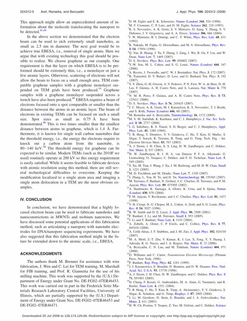
FIG. 5. Electron beam modification of a MWNT on a silicon nitride mem-brane. �a� TEM micrograph of an unmodified nanotube placed on the surfaceof a 50 nm low-stress silicon nitride membrane �scale of bar=100 nm�. Thegray colored background corresponds to the amorphous SiN membrane. Theimage is underfocused �creating white diffraction lines at the edges� to con-trast the nanotube against the amorphous layer. The black spots are from thedeposition process. �b� Close-up TEM micrograph of the unmodified tube ina scale of bar=20 nm. �c� TEM micrograph of the nanotube after modifi-cation with the electron beam of the TEM �scale of bar=100 nm�. �d�Close-up TEM micrograph of the modified nanotube with a nanohole �onthe left, �2.5�4 nm2� and two nanoconstrictions. In the nanoconstrictions,the silicon nitride can still be seen �scale of bar=20 nm�. Modification wasat room temperature.
FIG. 6. A TEM micrograph of a nanopore etched in a SiN membrane witha 200 keV focused electron beam �scale of bar=10 nm�. The white linesindicate the location of the MWNT. The hole is purposefully positioned neara MWNT. This sample design might be useful for experiments where mol-ecules or nanoparticles are translocated through the pore and detected orcharacterized with the nanotubes. This sample design might be useful forDNA/nanopore sequencing.
024312-4 Aref, Remeika, and Bezryadin J. Appl. Phys. 104, 024312 �2008�
Downloaded 25 Jul 2008 to 128.174.129.66. Redistribution subject to AIP license or copyright; see http://jap.aip.org/jap/copyright.jsp
This approach might allow an unprecedented amount of in-formation about the molecule translocating the nanopore tobe detected.41,44
In the above section we demonstrated that the electronbeam can be used to etch extremely small nanoholes, assmall as 2.5 nm in diameter. The next goal would be toachieve true EBESA, i.e., removal of single atoms. Here weargue that with existing technology this goal should be pos-sible to realize. We choose graphene as our example. Onerequirement is that the layer on which EBESA is to be per-formed should be extremely thin, i.e., a monolayer or just afew atomic layers. Otherwise, scattering of electrons will notallow the beam to focus on a small enough area. TEM com-patible graphene samples with a graphene monolayer sus-pended on TEM grids have been produced.14 Graphenesamples with a graphene monolayer suspended across atrench have also been produced.45 EBESA requires a beam ofelectrons focused onto a spot comparable or smaller than thedistance between the atoms in an atomic layer. The beam ofelectrons in existing TEMs can be focused on such a smallsize. Spot sizes as small as 0.75 Å have beendemonstrated.46 This is two times smaller than the smallestdistance between atoms in graphene, which is 1.4 Å. Fur-thermore, it is known for single wall carbon nanotubes thatthe threshold energy, i.e., the energy the electrons require toknock out a carbon atom from the nanotube, is80–140 keV.28 The threshold energy for graphene can beexpected to be similar. Modern TEMs �such as the 2010F weused� routinely operate at 200 kV so this energy requirementis easily satisfied. While it seems feasible to fabricate deviceswith atomic resolution using this method, there are still sev-eral technological difficulties to overcome. Keeping themodification localized to a single atom area and imaging asingle atom dislocation in a TEM are the most obvious ex-amples.
IV. CONCLUSION
In conclusion, we have demonstrated that a highly fo-cused electron beam can be used to fabricate nanoholes andnanoconstrictions in MWNTs and niobium nanowires. Wehave discussed some potential applications of this fabricationmethod, such as articulating a nanopore with nanotube elec-trodes for DNA/nanopore sequencing experiments. We havealso suggested that this fabrication method might in the fu-ture be extended down to the atomic scale, i.e., EBESA.
ACKNOWLEDGMENTS
The authors thank M. Brenner for assistance with wirefabrication, J. Wen and C. Lei for TEM training, M. Marshallfor FIB training, and Prof. R. Giannetta for the use of hismilling machine. This work was supported by the �U.S.� De-partment of Energy under Grant No. DE-FG02–07ER46453.This work was carried out in part in the Frederick Seitz Ma-terials Research Laboratory Central Facilities, University ofIllinois, which are partially supported by the �U.S.� Depart-ment of Energy under Grant Nos. DE-FG02–07ER46453 andDE-FG02–07ER46471.
1D. M. Eigler and E. K. Schweizer, Nature �London� 344, 524 �1990�.2M. F. Crommie, C. P. Lutz, and D. M. Eigler, Science 262, 218 �1993�.3K. S. Novoselov, A. K. Geim, S. V. Morozov, D. Jiang, Y. Zhang, S. V.Dubonos, I. V. Grigorieva, and A. A. Firsov, Science 306, 666 �2004�.
4J. W. Mintmire, B. I. Dunlap, and C. T. White, Phys. Rev. Lett. 68, 631�1992�.
5K. Nakada, M. Fujita, G. Dresselhaus, and M. S. Dresselhaus, Phys. Rev.B 54, 17954 �1996�.
6Q. Yan, B. Huang, J. Yu, F. Zheng, J. Zang, J. Wu, B. Gu, F. Liu, and W.Duan, Nano Lett. 7, 1469 �2007�.
7D. S. Novikov, Phys. Rev. Lett. 99, 056802 �2007�.8Y.-W. Son, M. L. Cohen, and S. G. Louie, Nature �London� 444, 347�2006�.
9A. Rycerz, J. Tworzdlo, and C. W. J. Beenakker, Nat. Phys. 3, 172 �2007�.10B. Trauzettel, D. V. Bulaev, D. Loss, and G. Burkard, Nat. Phys. 3, 192
�2007�.11S. Y. Zhou, G.-H. Gweon, A. V. Fedorov, P. N. First, W. A. de Heer, D.-H.
Lee, F. Guinea, A. H. Castro Neto, and A. Lanzara, Nat. Mater. 6, 770�2007�.
12N. M. R. Peres, F. Guinea, and A. H. Castro Neto, Phys. Rev. B 73,125411 �2006�.
13D. S. Novikov, Phys. Rev. B 76, 245435 �2007�.14J. C. Meyer, A. K. Geim, M. I. Katsnelson, K. S. Novoselov, T. J. Booth,
and S. Roth, Nature �London� 446, 60 �2007�.15M. Remeika and A. Bezryadin, Nanotechnology 16, 1172 �2005�.16M. S. M. Saifullah, K. Kurihara, and C. J. Humphreys, J. Vac. Sci. Tech-
nol. B 18, 2737 �2000�.17I. G. Salisbury, R. S. Timsit, S. D. Berger, and C. J. Humphreys, Appl.
Phys. Lett. 45, 1289 �1984�.18J. B. Heng, V. Dimitrov, Y. V. Grinkova, C. Ho, T. Kim, D. Muller, S.
Sligar, T. Sorsch, R. Twesten, R. Timp, and G. Timp, Tech. Dig. - Int.Electron Devices Meet. 03, 767 �2003�.
19A. J. Storm, J. H. Chen, X. S. Ling, H. W. Zandbergen, and C. Dekker,Nat. Mater. 2, 537 �2003�.
20H. W. Zandbergen, R. J. H. A. van Duuren, P. F. A. Alkemade, G.Lientschnig, O. Vasquez, C. Dekker, and F. D. Tichelaar, Nano Lett. 5,549 �2005�.
21S. Xu, M. Tian, J. Wang, J. Xu, J. M. Redwing, and M. H. W. Chan, Small1, 1221 �2005�.
22M. D. Fischbein and M. Drndic, Nano Lett. 7, 1329 �2007�.23J. Zhang, L. You, H. Ye, and D. Yu, Nanotechnology 18, 155303 �2007�.24M. Terrones, F. Banhart, N. Grobert, J.-C. Charlier, H. Terrones, and P. M.
Ajayan, Phys. Rev. Lett. 89, 075505 �2002�.25A. Hashimoto, K. Suenaga, A. Gloter, K. Urita, and S. Iijima, Nature
�London� 430, 870 �2004�.26P. M. Ajayan, V. Ravikumar, and J.-C. Charlier, Phys. Rev. Lett. 81, 1437
�1998�.27V. H. Crespi, N. G. Chopra, M. L. Cohen, A. Zettl, and S. G. Louie, Phys.
Rev. B 54, 5927 �1996�.28B. W. Smith and D. E. Luzzi, J. Appl. Phys. 90, 3509 �2001�.29F. Banhart, J. Li, and M. Terrones, Small 1, 953 �2005�.30J. Li and F. Banhart, Nano Lett. 4, 1143 �2004�.31A. Zobelli, A. Gloter, C. P. Ewels, and C. Colliex, Phys. Rev. B 77,
045410 �2008�.32A. Celik-Aktas, J. F. Stubbins, and J.-M. Zuo, J. Appl. Phys. 102, 024310
�2007�.33M. A. Meitl, Z.-T. Zhu, V. Kumar, K. J. Lee, X. Feng, Y. Y. Huang, I.
Adesida, R. G. Nuzzo, and J. A. Rogers, Nat. Mater. 5, 33 �2006�.34A. Bezryadin, C. N. Lau, and M. Tinkham, Nature �London� 404, 971
�2000�.35D. Williams and C. Carter, Transmission Electron Microscopy �Plenum
Press, New York, 1996�.36F. Banhart, Rep. Prog. Phys. 62, 1181 �1999�.37J. J. Kasianowicz, E. Brandin, D. Branton, and D. W. Deamer, Proc. Natl.
Acad. Sci. U.S.A. 93, 13770 �1996�.38A. J. Storm, J. H. Chen, H. W. Zandbergen, and C. Dekker, Phys. Rev. E
71, 051903 �2005�.39H. Chang, F. Kosari, G. Andreadakis, M. A. Alam, G. Vasmatzis, and R.
Bashir, Nano Lett. 4, 1551 �2004�.40J. B. Heng, C. Ho, T. Kim, R. Timp, A. Aksimentiev, Y. V. Grinkova, S.
Sligar, K. Schulten, and G. Timp, Biophys. J. 87, 2905 �2004�.41J. Li, M. Gershow, D. Stein, E. Brandin, and J. A. Golovchenko, Nat.
Mater. 2, 611 �2003�.42H. W. Ch. Postma, T. Teepen, Z. Yao, M. Grifoni, and C. Dekker, Science
024312-5 Aref, Remeika, and Bezryadin J. Appl. Phys. 104, 024312 �2008�
Downloaded 25 Jul 2008 to 128.174.129.66. Redistribution subject to AIP license or copyright; see http://jap.aip.org/jap/copyright.jsp
293, 76 �2001�.43L. Guo, E. Leobandung, and S. Y. Chou, Science 275, 649 �1997�.44M. Zwolak and M. D. Ventra, Nano Lett. 5, 421 �2005�.45J. S. Bunch, A. M. van der Zande, S. S. Verbridge, I. W. Frank, D. M.
Tanenbaum, J. M. Parpia, H. G. Craighead, and P. L. McEuen, Science315, 490 �2007�.
46P. E. Batson, N. Dellby, and O. L. Krivanek, Nature �London� 418, 617�2002�.
024312-6 Aref, Remeika, and Bezryadin J. Appl. Phys. 104, 024312 �2008�
Downloaded 25 Jul 2008 to 128.174.129.66. Redistribution subject to AIP license or copyright; see http://jap.aip.org/jap/copyright.jsp