Embed Size (px)
Citation preview
Linköping Studies in Science and TechnologyDissertation No. 667
STUDIES ON CMOSDIGITAL-TO-ANALOG CONVERTERS
J Jacob Wikner
Department of Electrical EngineeringLinköpings universitet, SE-581 83 Linköping, Sweden
Linköping 2001

Linköping Studies in Science and TechnologyDissertation No. 667
STUDIES ON CMOSDIGITAL-TO-ANALOG CONVERTERS
J Jacob Wikner
Department of Electrical EngineeringLinköpings universitet, SE-581 83 Linköping, Sweden
Linköping 2001

Studies on CMOS Digital-to-Analog Converters
Copyright © 2001 J Jacob Wikner
Department of Electrical EngineeringLinköpings universitet,SE-581 83 Linköping
ISBN91-7219-910-5 ISSN 0345-7524Printed in Sweden by UniTryck, Linköping, 2001
ainlySL)uired
t thes are
DACvesti-
staticspeed.neari-used
tches,encies.ency-noise-ctrumseveralpowerthe
ce it
ssionsasure-as lim-ns on
niquesistor-EM).
AbstractIn this thesis we present an overview and study on digital-to-analog converters (DAC), mfor communications applications. Especially, we look at some digital subscriber line (Dspecifications and communication over twisted-pair channels. It is pointed out that the reqresolution on the DACs in such systems is in the order of 12 to 14 bits of resolution. Asame time the bandwidth stretches from below MHz to several tens of MHz. These figurethe guiding specification throughout the thesis.
In this work we consider many of converter architectures and chips. The current-steeringis pointed out as a suitable converter for both high speed and high resolution. We also ingate the oversampling DAC (OSDAC) and discuss its properties in detail.
The performance of the converters is limited by both static and dynamic errors. Theerrors are usually caused by mismatch of the components and limit the accuracy at lowThe static performance is often described by measures of differential and integral nonlities, (DNL and INL). For communication applications these measures are not especiallyfor characterization of the DACs. Instead, the dynamic errors, such as settling errors, glietc., are more important since they increase with higher sample rates and signal frequTo analyze the effect of errors it is usually easier to consider the DAC’s behavior in frequdomain using measures, such as the spurious-free dynamic range (SFDR) and signal-toand-distortion ratio (SFDR). These measures are normally derived from the output spewhen a sinusoidal input signal is used. In some applications it may be necessary to usesinusoidal tones to get relevant measures. Two common measures are the multi-toneratio (MTPR) and the peak-to-average ratio (PAR). The PAR of the input signal affectsmaximum signal-to-noise ratio (SNR) of the converter and a small PAR is preferred sinmaximizes the SNR.
To help us understand how to design a converter several models and algorithmic expreare presented. The models are verified through simulations and partially through mements and experiments. Some of the most dominating error sources in converters, suchited output impedance, device mismatch, and noise, are highlighted. We give suggestiohow to reduce and minimize the influence of these types of error sources. These techinvolve calibration and randomization, as well as cancellation through for example pre-dtion algorithms. We also present the basics of dynamic element matching techniques (D
5
Abstract 6
funda-, wef the
ce hasmall
hes ine pro-ing
ed forixed-
e co-the
plica-e moste is todigital
tors tole ana-ect anh. Itprob-
fferentction
ferentand isthelinear
n terms
The usage of the models is to reduce the design time and get a good understanding formental limitations on performence. Instead of time-consuming circuit-level simulationspoint out the behavioral-level and algorithmic-level simulation of the converters. Most omodels have been described in languages, such as Matlab and Mathematica.
Several chips have been implementated in CMOS and some improvement in performanbeen measured from generation to generation. By comparing two similar DACs with svariations, we show how the performance of the converter depends on typical mismatcthe layout. The measurement results are analyzed by using simulation results from thposed DAC models. By identifying distortion terms we can partially determine matcherrors, output impedance, and parasitic impedance.
Often the design of DACs is focused on the actual converter alone. We emphasize the nea broad view, where a more integrated digital/analog design is considered. The typical msignal and analog circuits, e.g., DAC, ADC, filters, amplifiers. In e.g. a transceiver must boptimized. Analog circuits mix with digital circuits and signal processing algorithms onsame chip and we have to carefully investigate how the different subcircuits interact.
We discuss the design and implementation of current-steering DACs for wideband aptions. Different architectures are outlined and we emphasize the segmented DAC as thsuitable converter structure for high speed and high resolution. Here, a key design issufind the proper number of bits to encode into a thermometer code. This increases thecontents of the DAC, but reduces the glitches.
Further, we discuss issues involving design of OSDACs. We use the sigma-delta modulareduce the number of bits representing the digital signal and then we use small and simplog circuits, which can be optimized with respect to the device. As a design case, we selOSDAC for ADSL applications. It is found that the requirements on the OSDAC are tougis emphasized that the design of an oversampling converter essentially is a filter designlem. There is a large number of possible trade-offs that can be made between the dibuilding blocks in the OSDAC. Here, the key design issue is to define a proper cost funthat lets us find a good overall solution.
The thesis also presents some special converter architectures. A DAC’s behavior for difinput codes is examined. The thermometer code is the optimum code in terms of glitchessimplest for allowing interdigitized layout structures. However, for larger number of bits inencoder becomes rather large and complex. In the thesis we presentmore work where acode is used. This code ends up in-between the thermometer code and the binary code iof performance and complexity.

esis. Itronicemstmentged
., forcssoneters-nt todus-Erics-
avecom-
AcknowledgmentThere are so many to thank for supporting the work that has been compressed into this ththank all the members that have co-worked with me at Electronics Systems and ElecDevices at Linköping University and Ericsson Microelectronics AB, Ericsson Radio SystAB, and Ericsson Telecom AB. The head of the Electronics Systems group at the Deparof Electrical Engineering, Linköping University, Prof. Dr. Lars Wanhammar, is acknowledfor the support and the encouragement.
I especially want to thank Dr. Mikael Gustavsson and Dr. Nianxiong Tan, Globespan, Inctheir help and the needed boost throughout my work. Thanks to Dr. Yonghong Gao, EriRadio Systems AB, for the great help with oversampling converters. Thanks to Peter Pson, Ericsson Radio Systems AB, for the help with measurements on my first chips. I wathank Dr. Gunnar Björklund at the Ericsson Microelectronics Research Center for his intrial competence and clear view on research issues. Further on, I want to thank the smallson Microelectronics group at Linköping with which I have been working.
A large portion of Thank You to my parents, Christina and Lars-Erik, who – I guess – halways believed in (although not understood) what I have been doing. Thanks for all theputers you have given me throughout the years.
Thank you, Ulrica, for still letting me come home after all long working nights.
7

Acknowledgment 8

Abbreviations and AcronymsAC Alternating currentA/D Analog-to-digitalADSL Asymmetric digital subscriber lineADC Analog-to-digital converterAFE Analog front-endAHDL Analog high-level description languageAP AllpassAPK Amplitude-phase keyingASK Amplitude-shift keyingATM Asynchronous transfer modeAWGN Additive white Gaussian noise
BER Bit error ratebit Binary digitBP BandpassBSIM Simulation model
CAP Carrierless amplitude and phaseCD Compact discCDMA Carrierless division multiplexing accessCFT Clock feedthroughCMOS Complementary metal-oxide semiconductorCO Central officeCPE Customer’s premises equipmentCSFR Clock-to-signal frequency ratio
D/A Digital-to-analogDAC Digital-to-analog converter
9
Abbreviations and Acronyms 10
dB DecibeldBFS Decibel with respect to the full scale levelDC Direct currentDCVSL Differential clocking style logicDEM Dynamic element matchingDMT Discrete multi-toneDR Dynamic rangeDSL Digital subscriber lineDSP Digital signal processor
EDGE Enhanced data for GSM evolutionENOB Effective number of bitsERB Effective resolution bandwidth
FDM Frequency-division multiplexingFEXT Far-end crosstalkFFT Fast Fourier transformFIR Finite-length impulse responseFRDEM Full randomization dynamic element matchingFS Full scaleFSK Freqsuency-shift keying
GCN General cubic networkGPRS General packet radio serviceGSM Global system mobile telephonyGPIB General Purpose Interface BusGPRS General packet radio service
HD Harmonic distortionHDL High-level description languageHDTV High-definition televisionHP High pass
IFFT Inverse fast Fourier transformIFIR Interpolated finite-length impulse response filterIIR Infinite-length impulse responseIMD Intermodulation distortionI/O Input / outputI/Q In-phase and quadrature-phaseISDN Integrated services digital network
LP Lowpass

11 Abbreviations and Acronyms
LSB Least significant bitLSI Large-scale integration
MASH Multi-stageMF Multiple feedbackMOS Metal-oxide semiconductorMOSFET Metal-oxide semiconductor field effect transistorMSB Most significant bitMTPR Multi-tone power ratio
NEXT Near-end crosstalkNMOS N-channel metal-oxide semi-conductorNOB Number of bitsNSDEM Noise-shaping dynamic element matchingNTF Noise transfer function
OFDM Orthogonal frequency division multiplexingOP Operational amplifierOSADC Oversampled A/D converterOSDAC Oversampled D/A converterOSR Oversampling ratioOTA Operational transconductance amplifier
PAM Pulse-amplitude modulatedPAR Peak-to-average ratio or crest factorPCB Printed circuit boardPGC Programmable gain controlPDA Personal digital assistantPDP Power delay productPLL Phase-locked loopPMOS P-channel metal-oxide semi-conductorPOTS Plain old telephone servicePR Power ratioPRBS Pseudo-random binary sequencePRDEM Partial randomization dynamic element matchingPSD Power spectral densityPSK Phase-shift keying
QAM Quadrature amplitude modulation
R2Z Return-to-zeroRAM Random access memory
Abbreviations and Acronyms 12
ROM Read-only memoryRMS Root mean squareRX Receiver path
SC Switched capacitorS/H Sample-and-holdSUFR Signal-to-sample frequency ratioSFDR Spurious-free dynamic rangeSI Switched currentSNDR Signal-to-noise-and-distortion ratioSNR Signal-to-noise ratioSOC System on chipSQNR Signal-to-quantization noise ratioSR Slew rateSR Set-resetSTF Signal transfer function
TDM Time-division multiplexingTHD Total harmonic distortionTSPC True single-phase clockingTX Transmission path
ULSI Ultra-high large-scale integrationUMTS Universal mobile telecommunications system
VDSL Very high data rate DSLVLSI Very high large-scale integration
WCDMA Wideband CDMA
xDSL All/Any DSL

age,e/
le
Notation and NomenclatureIn general, throughout the thesis, an analog output value (current, voltor charge) from a D/A converter is denoted . The input digital codword is denoted and the corresponding bits in are denoted .Continuous-time signalsFourier transformation ofFourier transform of a continuous-time voltageLaplace transformation ofLaplace transform of a continuous-time voltageDiscrete-time signals or sequencesFourier transforms of a discrete-time signalz-transform (Laplace) of a discrete-time signal
-th Fourier coefficient of a discrete-time signalExpectation value of with respect to the entityNormal distribution with mean and standard deviationUniform distribution with mean and standard deviationExpected output value
, Wanted value of ,, Average value of ,, AC varying part of the input code/word
Update frequencySample frequency (equal to update frequency, )Nyquist frequency,Oversampling frequency
normalized angular frequency, sometimes also referred to as the angtransconductance of a CMOS transistoroutput conductance of a CMOS transistor
For relative errors, we use and for absolute errors.
AX X bi
x t( ) x τ( ) …, ,F * *V ω( ) v t( )L * *V s( ) v t( )x k( ) xk X k( ), ,X ωT( ) xX z( ) xX k( ) k xEδ * * δN µ σ,( ) µ σU µ σ,( ) µ σAX A X AX A X AX xf uf s f s f u=f N f N f u 2⁄ f s 2⁄= =f O u,
ωTgmgds
ε δ
13

Notation and Nomenclature 14

rts [
nde work
onallyheses
n,”
-
erg,-
ngx,
e of8.
theR-
Publications Related to the AuthorPublications Related to Thesis ChaptersMost of the work presented in the thesis has previously been published in internal repo1-9], theses [10-11], journals [12-17], and in conference proceedings [18-33]. Major parts of thework has been compiled in a text book[34]. However, in this thesis we present the backgrouto the results presented in these publications. Further, we have also extended some of thto cover more generalized problems. Some of the material has also resulted in patents [35-37].
Some of the results in publications – where the author is co-author – have been intentileft-out in the thesis and is to be more thoroughly examined in other students’ licentiate tand dissertations. The reader of this thesis is therefore also referred to references as “relatedwork” for further information on the topics.
List of Publications
Internal Reports at Linköping University[1] H. Träff and J.J. Wikner, “Snapshot Sampling for Ultra-High Speed Data Acquisitio
LiTH-ISY-R-1933, Linköping University, Sweden, March 1997.[2] J.J. Wikner and N. Tan, “Modelling of DACs for Telecommunication,” LiTH-ISY-R
1983, Linköping University, Sweden, Sept. 1997.[3] M. Karlsson, O. Gustafsson, J.J. Wikner, T. Johansson, W. Li, M. Hörlin, and H. Ekb
“Understanding Multiplier Design Using ‘Overturned-Stairs’ Adder Trees,” LiTH-ISYR-2016, Linköping University, Sweden, Feb. 1998.
[4] M. Karlsson and J.J. Wikner, “Variations of ‘Fast Filter’ Implementations UsiDifferent DFL Descriptions in Mentor Graphics Design Tools,” LiTH-ISY-R-2xxLinköping University, Sweden, May. 1998.
[5] J.J. Wikner and N. Tan, “Influence of Parameter Variations on the PerformancCurrent-Steering DACs,” LiTH-ISY-R-2074, Linköping University, Sweden, Nov. 199
[6] J.J. Wikner and N. Tan, “Comparison of the Impact of Matching Errors onPerformance of Current-Steering CMOS Digital-to-Analog Converters,” LiTH-ISY-2075, Linköping University, Sweden, Nov. 1998.
15
Publications Related to the Author 16
for
forty,
R-
sis
ns7-1,
n,”
or
of
L
or
D/Ag
ic
or98,
D/A,
[7] J.J. Wikner, Y. Gao, and N. Tan, “A 3.3V CMOS Oversampling D/A ConverterDMT-ADSL,” LiTH-ISY-R-2076, Linköping University, Sweden, Nov. 1998.
[8] J.J. Wikner, “A Chipset Consisting of 15 CMOS Wideband D/A ConvertersTelecommunications. Design and Study,” LiTH-ISY-R-2xxx, Linköping UniversiSweden, Nov. 1998.
[9] J.J. Wikner, “Measurement and Simulations of a CMOS DAC Chipset,” LiTH-ISY-2xxx, Linköping University, Sweden, Dec. 1998.
Theses[10] J. J. Wikner,Measuring and Specification of Integrated Analog Circuits - with empha
on measuring Analog-to-Digital and Digital-to-Analog Converters, M.Sc. thesis,Linköping University, Nov. 1996.
[11] J. J. Wikner,CMOS Digital-to-Analog Converters for Telecommunication Applicatio,Linköping studies in science and technology, Thesis No. 715, ISBN 91-7219-27Linköping, Aug. 1998.
Journal Papers[12] H. Träff and J.J. Wikner, “Snapshot Sampling for Ultra-High Speed Data Acquisitio
Electronics Letters, vol. 33, no. 13, p. 1137-9, June 1997.[13] N. Tan and J.J. Wikner, “A CMOS Digital-to-Analog Converter Chipset f
Telecommunications,”IEEE Magazine of Circuits & Devices, vol. 13, no. 5, p. 11-6,Sept. 1997.
[14] J.J. Wikner and N. Tan, “Influences of Circuit Imperfections on the PerformanceDACs,” Analog Integrated Circuits and Signal Processing, no. 1, Jan. 1999.
[15] J.J. Wikner, Y. Gao, and N. Tan, “D/A Conversion Interface Design for DMT-ADSApplications,”IEEE Magazine of Circuits & Devices, vol. 1, no. 6, p. 7-13, Nov. 1998.
[16] J.J. Wikner and N. Tan, “Modeling of CMOS Digital-to-Analog Converters fTelecommunication,”IEEE Transactions on Circuits and Systems II, vol..46, no. 5,p. 489-99, May 1999.
[17] Y. Gao, J.J. Wikner, and H. Tenhunen, “Design and Analysis of an OversamplingConverter in DMT-ADSL Systems,”Analog Integrated Circuits and Signal Processin,2001.
Conference Papers[18] J.J. Wikner and N. Tan, “Influences of Circuit Imperfections on the Dynam
Performance of DACs,” inProc. 17th NorChip Conference, Tallinn, Estonia, Nov. 10-11,1997.
[19] J.J. Wikner and N. Tan, “Modelling of CMOS Digital-to-Analog Converters fTelecommunication,” inProc. IEEE Symposium on Circuits and Systems 19ISCAS’98, vol. 1, p. 25-8, Monterey, USA, May 30 - June 3, 1998.
[20] Y. Gao, J.J. Wikner, and H. Tenhunen, “Design and Analysis of an OversamplingConverter for DMT-ADSL Systems,” inProc. IEEJ 3rd Analog VLSI WorkshopAVLSIWS’99, Taiwan, May, 1999.
[21] J.J. Wikner, “Design and Implementation of Current-Steering CMOS DACs,”in Proc.RVK’99 (Radiovetenskapskonferensen), Karlskrona, Sweden, June 1999.
17 Publications Related to the Author
ring
ent
ing
enton
,” in
ACd
,” in
ent
AC
/Ad
ion
s
nt
[22] J.J. Wikner, “Simulation and Measurement of Two 3-5V CMOS Current-SteeDACs,” in Proc. IEE 3rd International A/D and D/A Conference, p. 130-3, Glasgow,Scotland, July 28, 1999
[23] K.O. Andersson and J.J. Wikner, “Modeling of the Influence of Graded ElemMatching Errors in CMOS Current-Steering DACs,” inProc. 17th NorChip Conference,Oslo, Norway, Nov. 8-9, 1999.
[24] N.U. Andersson and J.J. Wikner, “Comparison of Different Dynamic Element MatchTechniques for Wideband CMOS DACs,” inProc. 17th NorChip Conference, Oslo,Norway, Nov. 8-9, 1999.
[25] N.U. Andersson and J.J. Wikner, “A Strategy of Implementing Dynamic ElemMatching in Current-Steering DACs,“ inProc. IEEE 2000 Southwest SymposiumMixed-Signal Design, SSMSD’00, p. 51-6, San Diego, CA, USA, Feb. 2000.
[26] J.J. Wikner and M. Vesterbacka, “D/A Conversion with Linear-Coded Weights,” inProc.IEEE 2000 Southwest Symposium on Mixed-Signal Design, SSMSD’00, p. 61-6, SanDiego, CA, USA, Feb. 2000.
[27] J.J. Wikner and M. Vesterbacka, “Characteristics of Linear-Coded D/A ConvertersProc. IEEE 2000 Southwest Symposium on Mixed-Signal Design, SSMSD’00, p. 67-72,San Diego, CA, USA, Feb. 2000.
[28] K.O. Andersson and J.J. Wikner, “Characterization of a CMOS Current-Steering Dusing State-Space Models,“ inProc. IEEE 2000 Midwest Symposium on Circuits anSystems, MWSCAS’00, Lansing, MI, USA, Aug. 2000.
[29] M. Vesterbacka and J.J. Wikner, “Characteristics of Linear-Coded D/A ConvertersProc. IEEJ 4th Analog VLSI Workshop, AVLSIWS’00, Stockholm, Sweden, June 2000.
[30] M. Vesterbacka, M. Rudberg, J.J. Wikner, and N.U. Andersson, “Dynamic ElemMatching in D/A Converters with Restricted Scrambling,” inProc. IEEE 7thInternational Conference on Electronics, Circuits, and Systems, ICECS’00, Beirut,Lebanon, Dec. 17-20, 2000.
[31] K.O Andersson, N.U. Andersson, and J.J. Wikner, “Spectral Shaping of DNonlinearity Errors through Modulation of Expected Errors,” to appear inProc. IEEE2001 International Symposium on Circuits and Systems, ISCAS’01, Sydney, Australia,May 6-9, 2001.
[32] M. Vesterbacka and J.J. Wikner, “Design of Encoders for Linear-Coded DConverters,” to appear inProc. IEEE 2001 International Symposium on Circuits anSystems, ISCAS’01, Sydney, Australia, May 6-9, 2001.
[33] M. Rudberg, M. Vesterbacka, N.U. Andersson, and J.J. Wikner, “Glitch Minimizatand Dynamic Element Matching in D/A Converters,” inProc. IEEE 7th InternationalConference on Electronics, Circuits, and Systems, ICECS’00, Beirut, Lebanon, Dec. 17-20, 2000.
Book[34] M. Gustavsson, J.J. Wikner, and N. Tan,CMOS Data Converters for Communication,
Kluwer Academic Publishers, Jan. 2000.
Patents[35] N. Tan, J. Erlands, and J.J. Wikner, “A Differential Line Driver“, Swedish pate
9800635-6 and U.S. patent pending, 1998.

Publications Related to the Author 18
dish
ent
[36] J.J. Wikner and M. Vesterbacka, “D/A Conversion Method and D/A Converter”, Swepatent 9903500-8, U.S. patent pending, Oct. 1999.
[37] N. U. Andersson, M. Vesterbacka, J. J. Wikner, and M. Karlsson Rudberg, “Improvemof segmented DACs,” Swedish patent 0001917-4 U.S. patent pending, May 2000.
Table of Contents
1 Introduction . . . . . . . . . . . . . . . . . . . . . . .1
1.1 Integrated Circuits and the Digital/Analog Interface 4
1.1.1 Digital Circuits 51.1.2 Analog Circuits 61.1.3 Mixed-Signal Circuits 8
1.2 Communication Circuits 8
1.2.1 Modulation Schemes 9Quadrature Amplitude Modulation (QAM)
1.2.2 Channel Models 101.2.3 Transmission Modes 11
1.3 Digital Subscriber Line Technique (DSL) 11
1.3.1 DSL Analog Front End (AFE) 121.3.2 Discrete Multi-Tone (DMT) Signals in DSL 13
Frames and cyclic prefix1.3.3 Spectral Requirements for ADSL and VDSL 201.3.4 The Twisted-Pair Channel 20
Crosstalk
1.4 Requirements on D/A Converters for xDSL 22
1.5 Data Converter Applications 23
2 Introduction to D/A Conversion . . . . . . . . . . . .25
2.1 Introduction 25
2.2 The Ideal D/A Converter 26
2.2.1 Ideal Transfer Function 282.2.2 Codes for D/A Conversion 29
2’s complementOffset binarySigned-digit“Walking one”Thermometer codeLinear code
2.3 Static Performance 31
2.3.1 Quantization or Truncation Noise 312.3.2 Offset Error 342.3.3 Gain Error 352.3.4 Differential (DNL) and Integral Nonlinearity (INL) 372.3.5 Monotonic Behavior 392.3.6 Nonuniform Quantization 40
i
Table of Contents ii
2.4 Dynamic Performance 42
2.4.1 Nonlinear Settling 442.4.2 Glitches 452.4.3 Clock Feedthrough (CFT) 47
2.5 Frequency-Domain Measures 48
2.5.1 Harmonic Distortion (HDk) 502.5.2 Total Harmonic Distortion (THD) 502.5.3 Signal-to-Noise Ratio (SNR) 502.5.4 Signal-to-Noise and Distortion Ratio (SNDR) 502.5.5 Spurious-Free Dynamic Range (SFDR) 512.5.6 Effective Number Of Bits (ENOB) 512.5.7 Multi-Tone Power Ratio (MTPR) 512.5.8 Intermodulation Distortion (IMD) 522.5.9 Linearity as Function of Amplitude and Frequency 52
Dynamic range (DR)Effective resolution bandwidth (ERB)
2.5.10 Peak-to-Average Ratio (PAR) 54
3 D/A Converter Architectures . . . . . . . . . . . . .55
3.1 Introduction 55
3.2 Nyquist-Rate D/A Converters 56
3.3 Interpolating D/A Converters 57
3.3.1 Gain in Resolution Using Interpolation 60
3.4 Oversampling D/A Converters (OSDACs) 62
3.4.1 Noise-Shaping Modulators 62Interpolative or multiple-feedback modulator
3.4.2 Improvement in Resolution Using Noise-Shaping 66
3.5 DAC Architectures 67
3.5.1 Binary-Weighted DAC Architecture 683.5.2 Thermometer-Coded DAC Architecture 683.5.3 Direct Encoded DAC Architecture 693.5.4 Linear-Coded DAC Architecture 703.5.5 Hybrid DAC Architectures 703.5.6 Algorithmic DAC Architecture 71
Pipelined algorithmic DAC
3.6 Common DAC Circuit Implementations 72
3.6.1 Current-Steering DAC 733.6.2 Charge-Redistribution DAC 743.6.3 R-2R Ladder DAC 743.6.4 Resistor-String DAC 753.6.5 Switched-Current Algorithmic DAC 75
3.7 DAC Comparison 77
iii Table of Contents
4 Behavioral-Level Models for Current-Steering,Nyquist-Rate D/A Converters . . . . . . . . . . . . .81
4.1 Introduction 81
4.2 Unit-Element Approach 84
4.2.1 Matching Errors of Unit Current Sources 85
4.3 Limited Output Impedance 87
4.3.1 Settling-Time Error with Ideal Current Sources 954.3.2 Static Error Current 984.3.3 DNL and INL as Function of the Output Resistance 984.3.4 SNDR as Function of the Output Resistance 1004.3.5 SFDR as Function of the Output Resistance 1034.3.6 Influence of Parasitic Resistance 1074.3.7 SNDR and SFDR as Functions of the Output Impedance 1084.3.8 Influence of Parasitic Impedance 109
4.4 Influence of Circuit Noise 110
4.5 Current Source Mismatch 113
4.5.1 SNDR as Function of the Stochastic Mismatch Errors 1154.5.2 SFDR as Function of the Stochastic Mismatch Errors 117
Influence of segmentation and thermometer code4.5.3 SNDR and SFDR as Function of the Graded and
Correlated Mismatch Errors 121
4.6 Glitches and Influence of Bit Skew 122
5 Current-Steering D/A Converters . . . . . . . . . .127
5.1 Introduction 127
5.2 Current-Steering DAC Architectures 128
5.2.1 Flat and Folded Array Structures 1295.2.2 Segmented Structures 1315.2.3 Encoded Array Structures 133
5.3 Practical Design Considerations 134
5.3.1 Unit Current Source 134Output impedanceMatching
5.3.2 Current Switches 139On-resistanceClock feedthrough (CFT)Switching signalsSwitch memory
5.3.3 Digital Circuits 143Segmentation circuits
5.3.4 Mixed-Signal Design 145
Table of Contents iv
5.4 CMOS Current-Steering DACs for VDSL Applications 147
5.4.1 Current Sources and Bias 147Bias and supply networkMatching considerations
5.4.2 Current Switches 1495.4.3 Digital Circuits 1495.4.4 Chip Implementations 150
5.5 Measurement Results 150
5.5.1 Measurement Setup and Techniques 152Test signal generation
5.5.2 Measured Results 154Single-ended vs. differential outputsComparison of two generation DACs
5.5.3 Measured, Calculated, and Simulated Results 157General considerationsOutput impedanceDevice matchingMeasurement conclusions
6 Oversampling D/A Converters. . . . . . . . . . . .161
6.1 Introduction 161
6.2 OSDAC Building Blocks 161
6.2.1 Interpolator and Interpolation Filters 164Cascaded accumulator structure
6.2.2 Noise-Shaping Modulator 169Multiple-feedback modulatorsMulti-stage modulators (MASH)
6.2.3 M-bit DAC 174One-bit DAC and semi-digital FIR filter
6.2.4 Interpolated Semi-Digital FIR Filter 1766.2.5 Image-Rejection and LP Filter 177
6.3 Simulation Results of OSDAC Blocks 178
6.3.1 DMT-ADSL Input Signal 1806.3.2 Interpolation Filters 1806.3.3 Noise-Shaping Modulators 1826.3.4 Semi-Digital FIR Filters and Image-Rejection Filter 184
6.4 A CMOS Current-Steering 5th-OrderOSDAC for DMT-ADSL 185
6.4.1 Semi-Digital FIR Filter 185Unit current sourceCurrent switchesD-latchesFilter taps
6.4.2 Complete Chip Layout 189
v Table of Contents
7 Special Techniques for Enhanced D/A Conversion 191
7.1 Introduction 191
7.2 Nonlinear Error Compensation 192
7.2.1 Pre-Distortion Circuits 1937.2.2 Combinations and Variations on Linearization Techniques 196
7.3 Current Source Calibration 197
7.4 Dynamic Element Matching (DEM) Techniques 199
7.4.1 Dynamic Randomization 2007.4.2 Dynamic Element Matching (DEM) with Encoder 202
Full-randomization DEM (FRDEM)Partial-randomization DEM (PRDEM)Noise-shaping DEM (NSDEM)Performance comparison
7.4.3 Dynamic Randomization with Reduced Glitching 205Generalized cubic network (GCN)Hardware Efficient dynamic randomization with reduced glitching
7.5 Special Codes in DACs 208
7.5.1 Linear-Coded DACs 209Weight distributionEncoder complexityGlitch performanceDual linear-coded approachLayout consideration
7.5.2 Signed-Digit Coded DACs 2157.5.3 Return-to-Zero Code 217
8 Appendices . . . . . . . . . . . . . . . . . . . . . .219
8.1 Introduction 219
8.2 Resolution Improvement Through Noise Shaping 219
8.3 SNDR and SFDR as Functions of Output Conductance 221
8.4 Fourier Series Coefficients for the MSBs of Sinusoid Inputs 228

Table of Contents vi
List of Figures
g the
ll-
l side,
MT
gnal.
DSL.
al.
put.
hout
nd
(b)
ical
inear
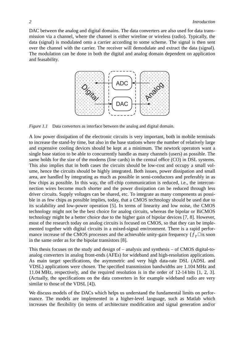
1 Introduction1.1, p. 2: Data converters as interface between the analog and digital domain.1.2, p. 8: Switching noise from digital circuits is spreading through the substrate and affectin
sensitive analog circuits.1.3, p. 9: Illustration of a communication system.1.4, p. 10: 16-QAM code constellation in the IQ-space. The point (3,1) is high-lighted.1.5, p. 10: Example of a model of a memoryless Gaussian channel.1.6, p. 11: Illustration of different transmission modes. (a) simplex, (b) half-duplex, and (c) fu
duplex.1.7, p. 12: Illustration of a DSL communication system.1.8, p. 13: DSL analog front-end.1.9, p. 14: Examples on echo cancelling techniques (dashed). On (a) the analog side, (b) digita
(c) using and (d) passive hybrid.1.10, p. 15: Example of a multi-tone signal in the (a) time and (b) frequency domain1.11, p. 17: Example of a multi-tone signal with (a) high and (b) low PAR.1.12, p. 18: Illustration of Gaussian distributed amplitude levels of (a) high- and (b) low-PAR D
signals.1.13, p. 18: Standard deviation of amplitude distribution as function of PAR for a multi-tone si1.14, p. 19: Clipping probability as function of the PAR.1.15, p. 19: Use of cyclic prefix in transmission in batches.1.16, p. 20: Transmitted power spectral density specifications on (a) CO and (b) CPE side for A1.17, p. 22: Input impedance of a twisted-pair cable as function of frequency and length.1.18, p. 23: Overview of application areas as function of resolution and sample frequency.
2 Introduction to D/A Conversion2.1, p. 26: Alternative representations of ideal DACs.2.2, p. 27: Image-rejection filter (LP) is used at the output of the DAC to reconstruct the sign2.3, p. 27: Output signal spectrum with images at centers of the update frequency.2.4, p. 28: Output amplitude levels as function of the input digital codes.2.5, p. 32: Transfer function (a) and quantization error (b) for a 3-bit DAC when ramping the in
Solid lines illustrate the actual behavior and dashed lines the ideal behavior.2.6, p. 34: Output amplitude levels as function of the input digital codes with (dashed) and wit
(solid) errors for a 3-bit DAC.2.7, p. 35: Characteristics of (a) linear and (b) nonlinear DAC gain error.2.8, p. 37: (a) Nonideal transfer characteristics illustrating INL and DNL errors in a 3-bit DAC a
(b) compensated transfer characteristics.2.9, p. 39: (a) DNL and (b) INL for the transfer function shown in Fig. 2.8.2.10, p. 40: Example of a transfer function of a nonmonotonic DAC.2.11, p. 40: DC transfer characteristics of a DAC with nonuniform quantization.2.12, p. 43: Actual output signal and ideal output signal (dashed) of a DAC.2.13, p. 46: Glitch modeled as a pulse with height Xg and duration Tg.2.14, p. 48: Illustration of the effect of clock feedthrough on MOS switches. (a) MOS switch and
typical output signal.2.15, p. 49: Frequency spectrum of a single-tone output signal from a nonlinear DAC with typ
frequency-domain measures.2.16, p. 49: Frequency spectrum of a (a) dual-tone and (b) multi-tone output signal from a nonl
DAC with typical frequency-domain measures.
vii
List of Figures viii
les of
ratio.
trum
) and
ratio.
oded
s. the
-W
d)
may
e find
nd (b)
2.17, p. 53: Typical SNDR and SFDR vs. amplitude level for a 14-bit DAC.2.18, p. 53: Measured SFDR as function of update and signal frequencies.
3 D/A Converter Architectures3.1, p. 56: (a) Output spectrum from a Nyquist-rate DAC. The images are centered at multip
the update frequency. (b) DAC with an image-rejection filter (LP).3.2, p. 57: Sinc attenuation of the output signal as function of the signal to sampling frequency3.3, p. 58: Interpolator without (a) and with (b) filters (interpolation filters).3.4, p. 59: Illustration of interpolation of order 4. The original spectrum, the interpolated spec
with filtering (dashed), and the final interpolated signal are shown.3.5, p. 60: Interpolation together with lower-resolution DAC where theN-M LSBs are discarded.3.6, p. 62: OSDAC including interpolation, modulation, and filtering.3.7, p. 63: Different sigma-delta modulators. (a) Signal feedback and (b) error feedback. In (c
(d) we find the respective noise models for the quantization error in (a) and (b),respectively.
3.8, p. 64: First-order modulators using (a) signal- and (b) error-feedback.3.9, p. 65: Power spectral density for 1st-, 2nd-, and 3rd-order modulators.3.10, p. 65: Interpolative or multiple-feedback modulator structure.3.11, p. 67: Simulated achievable ENOB as function of the modulator order and oversampling3.12, p. 68: General algorithm for converting codes.3.13, p. 69: Illustrations of the (a) binary-weighted, (b) thermometer-coded, and (c) direct enc
DAC architectures.3.14, p. 71: Hybrid DACs use a combination of a number of different types of DACs.3.15, p. 71: Schematic view of an algorithmic DAC.3.16, p. 72: Pipelined algorithmic DAC.3.17, p. 73: An N-bit binary-weighted current-steering DAC with output buffer.3.18, p. 74: Example of anN-bit charge-redistribution DAC without reset phase.3.19, p. 75: An N-bit R-2R ladder DAC.3.20, p. 76: AnN-bit resistor string DAC whereM=2N-1.3.21, p. 76: A switched-current (SI) implementation of an algorithmic DAC.3.22, p. 78: Reported measured performance of different DAC types. In (a) the performance v
update frequency and in (b) vs. the signal frequency (bandwidth).
4 Behavioral-Level Models for Current-Steering, Nyquist-Rate D/A Con-verters4.1, p. 83: AnN-bit binary weighted current-steering DAC. The output is terminated over a 50
load.4.2, p. 84: (a) Symbols for two capacitors. (b) Unit element capacitors. (c) Individual layout. (
Even distribution of unit element capacitors.4.3, p. 85: Variation of oxide thickness over the wafer and the individual chips. The thickness
vary significantly over the wafer, but may be approximated by a plane for smalldimensions.
4.4, p. 86: PMOS implementation of a unit current source.4.5, p. 88: Generalized view of a differential-mode current-steering DAC.4.6, p. 89: Linearized model of the unit current source (a) with and (b) without parasitics from
switches and interconnection wires.4.7, p. 90: Change of input signal causes additional sources to be connected to the output. W
the situation before (a) and after (b) the switching instant.4.8, p. 94: Output (a) step response for the positive output with ideal step shown (dashed) a
corresponding error current.4.9, p. 95: Output spectra for (a) lower and (b) higher signal frequencies.
ix List of Figures
–8.
R as
AC
DR as
e LSB
iation
rror
ion of
bit
the
and
C.
e
ply
d the
tion.t DC
ion.sible
4.10, p. 95: Simulated SFDR as function of signal frequency.4.11, p. 98: (a) Single-ended and (b) differential output spectra with a conductance ratio of 104.12, p. 100: Simulated DNL and INL as a function of input code for a resistance ratio of 108.4.13, p. 102: Simulated (solid) and calculated (dashed) (a) single-ended and (b) differential SND
function of the conductance ratio for 10-, 12-, and 14-bit DACs.4.14, p. 103: Simulated (solid) and calculated (dashed) single-ended SNDR as function of the
level.4.15, p. 106: Simulated (solid) and calculated (dashed) (a) single-ended and (b) differential SF
function of the conductance ratio for 10-, 12-, and 14-bit DACs.4.16, p. 107: (a) Model of the current source at bit positionk with parasitic resistance, Rpar,k, from
switches and internal wires and (b) modified model.4.17, p. 109: Measured and simulated SFDR as function of the signal and update frequencies.4.18, p. 110: Unit current source with noise current source, diu,m.4.19, p. 112: Simulated (solid) and calculated (dashed) single-ended SNR as function of the th
current for a 14-bit DAC.4.20, p. 114: Modeling of current source with error current source, DIu,m.4.21, p. 116: Output spectrum for a 14-bit DAC with approximate mismatch error standard dev
of 1.5 %.4.22, p. 117: Calculated (dashed) and simulated (dashed) SNDR as function of the mismatch e
standard deviation for 10-, 12-, and 14-bit DACs.4.23, p. 119: Transient behavior of the individual bits when applying a full-scale sinusoid.4.24, p. 120: Simulated SNDR as function of the input amplitude for mismatch standard deviat
5%.4.25, p. 121: Calculated and simulated SFDR as function of the mismatch for 10-, 12-, and 14-
DACs.4.26, p. 122: Layout of the unit current sources in a folded array structure.4.27, p. 124: Model of timing uncertainty. The ideal switching signal (dashed) is compared with
actual signal (solid). In (a) a linearized model and in (b) a box model.4.28, p. 125: Simulated output spectrum for (a) ideal signal, (b) randomly varying glitch model,
(c) fixed glitch model.
5 Current-Steering D/A Converters5.1, p. 128: Principle of an N-bit current-steering DAC.5.2, p. 129: (a) “Flat” and (b) “folded” array layout of unit current sources.5.3, p. 130: Influence of gradients for a (a) flat layout approach on the (b) INL.5.4, p. 131: Influence of gradients for a (a) distributed layout approach on the (b) INL.5.5, p. 132: Illurstration of a segmented current source array. TheM binary MSBs are encoded intoT
= 2M–1 thermometer coded bits.5.6, p. 132: Estimated glitch power as function of the number of segmented bits in a 14-bit DA5.7, p. 133: Unit current source array with decoding circuits.5.8, p. 134: Schematic view of PMOS current sources using (a) single transistor and (b) singl
cascode, and (c) double cascode.5.9, p. 136: Simulated output impedance of three different unit current source configurations.5.10, p. 138: Simulated output impedance of the unit current sources as function of the (a) sup
voltage and (b) output DC voltage level.5.11, p. 139: Model of the voltage supply wire connected to a number of DAC current sources an
drop of accuracy in the currents.5.12, p. 139: Differential current switch as (a) circuit model and (b) MOS transistor implementa5.13, p. 141: Simulated switch on-impedance as function of the (a) supply voltage and (b) outpu
voltage.5.14, p. 141: Transmission gates used as current switches.5.15, p. 142: Dummy transistor used in the switch to reduce the effect of channel charge inject5.16, p. 143: (a) Wanted switch signals for a differential current switch and (b) and (c) show pos
List of Figures x
ND
by (b)
ing n-
ource.
gnald.
in (a)
uble
r for a
ignal
e
log
ut ofut
.
rs. (b)ilter
nd
circuit implementations generating overlapping signals.5.17, p. 144: Iterative implementation of a binary-to-thermometer encoder. Note that there is A
and OR gates in parallel.5.18, p. 145: Example of a 2-to-3 encoder with AND-OR pair (a). Same encoder implemented
2-2 multiplexers. (c) Pass-transistor implementation of the 2-2 multiplexer.5.19, p. 145: Shielding of sensitive analog blocks by using guard rings.5.20, p. 146: Shielding of sensitive analog signal wires (a) by using ground wires and (b) also us
doped substrate layer in the p-substrate underneath the wires.5.21, p. 146: Separation of analog and digital pins at the board level.5.22, p. 148: Layout view of a (a) double-cascoded and (b) single-cascoded PMOS unit current s5.23, p. 149: (a) Cascoded and (b) wideswing PMOS current mirror bias circuits.5.24, p. 150: Layout view of a differential current switch for the LSBs.5.25, p. 151: Chip photograph of the 14-bit current-steering 0.60-mm CMOS DAC.5.26, p. 151: Chip photograph of the 12-bit current-steering 0.25-mm CMOS DAC.5.27, p. 153: View of a measurement system.5.28, p. 154: Output amplitude spectra from a 14-bit DAC with (a) ideal input signal, (b) clipped si
at 99.9% of its maximum value, and (c) repeated signal but with its period truncate5.29, p. 155: Measured differential output spectra from (a) DAC A and (b) DAC B.5.30, p. 156: Measured SFDR for different update frequencies. The results for DAC A is shown
and for DAC B in (b). The supply voltages are 3.3 and 5 V.5.31, p. 156: Measured SFDR for DAC C as function of the signal and update frequency.5.32, p. 157: Comparison of the measured SFDR from DAC A and C.5.33, p. 157: Part of current source array for the (a) second and (b) third generation DAC with do
cascode current sources.5.34, p. 158: (a) Measured power in the fundamental, 2nd, and 3rd harmonics vs. signal powe
14-bit DAC and in (b) derived harmonic distortion from the results in (a).5.35, p. 159: (a) Measured output spectrum for a 14-bit DAC. Update frequency is 25 MHz and s
frequency 670 kHz. The input amplitude level is –15 dBFS.5.36, p. 160: Simulated output spectrum for a 14-bit DAC with similar conditions as used for th
measured DAC result in Fig. 5.35.
6 Oversampling D/A Converters6.1, p. 162: Generalized OSDAC architecture including interpolator, modulator, DAC, and ana
LP filter.6.2, p. 163: Example spectra for different signals in an OSDAC with OSR = 8: (a) Original inp
spectrum, (b) interpolated spectrum, (c) filtered interpolated signal, (d) introductionnoise by the modulator, (e) same as (d), but with logarithmic axis, and (f) final outpsignal.
6.3, p. 165: One-stage FIR interpolation filter. The delayTo is related to the oversampling frequency6.4, p. 165: Principle description of multi-stage interpolation filtering.6.5, p. 166: Illustration of normalized sinc-weighting through S/H interpolation.6.6, p. 167: Interpolation filter structure using differentiators, D(z), and accumulators, A(z).6.7, p. 168: (a) A filter is compensating the large loss within the passband due to the sinc filte
Simulated characteristics of the sinc filter (dotted) and the result with compensation f(solid).
6.8, p. 169: Basic structure of signal- and error-feedback modulators.6.9, p. 170: Simulated modulator output (solid) for ramped input (dashed) for (a) 1st and (b) 2
order.6.10, p. 171: General multiple-feedback modulator of higher order (N).6.11, p. 171: General multiple-feedback modulator with feedforward coefficients,c.6.12, p. 173: Root locus for a 4th-order MF modulator without theai feedback zeros.6.13, p. 174: Two-stage 4th-order modulator structure using two 2nd-order modulators.
xi List of Figures
hing
IFIR
itional
d 32.es the
(a) 3,
t
cting
d (c)
withand
of
and
with
bits.on of
oded
6.14, p. 175: DC transfer characteristcs of a one-bit DAC with (solid) and without (dashed) matcerrors.
6.15, p. 175: Cascaded one-bit DACs forming aK-tap FIR filter structure.6.16, p. 177: Magnitude responses for an FIR filter and an interpolated (4 times) FIR filter. The
has a 5-dB offset for illustration.6.17, p. 178: Images are rejected and noise attenuated with (a) continuous-time filter and (b) add
discrete-time filters.6.18, p. 179: Filtering functions in the of the OSDAC output signal, illustrated in the frequency
domain.6.19, p. 181: 256-tone DMT Input signal.6.20, p. 181: Magnitude responses of (a) Cauer and (b) FIR interpolation filters for OSR = 16 an
Solid lines indicate the 0.5-dB specification on the passband ripple and dashed lin0.1-dB specification.
6.21, p. 183: Examples on modulator output spectra for single-tone inputs. Modulator orders are(b) 4, (c) 5 for OSR = 32 and in (d) a 5th-order modulator for OSR = 16.
6.22, p. 184: Magnitude response of the semi-digital FIR filter, SD FIR I, (a) with and (b) withoutruncated coefficients.
6.23, p. 186: (a) Current-steering implementation of a semi-digital filter with coefficient lengthK. (b)Differential current switches where negative coefficients are realized by cross connethe outputs.
6.24, p. 188: Impulse response from a circuit-level simulation of the semi-digital FIR filter.6.25, p. 189: Transistor schematics of (a) P- and (b) N-type latches.6.26, p. 189: Die photograph view of the OSDAC with modulator and semi-digital FIR filter.
7 Special Techniques for Enhanced D/A Conversion7.1, p. 192: Error cancellation by using an inverse function (a) at the input, (b) at the output, an
compensating DAC in parallel.7.2, p. 195: Use of comparators in a hardware-efficient pre-distortion circuit.7.3, p. 196: Output spectra from a nonlinear DAC without (a) pre-distortion, and (b) through (d)
pre-distortion. In (b) we use complete inverse function, (c) comparator pre-distortion,(d) pre-distortion with Taylor expansion.
7.4, p. 197: Use of loops and adaptation for pre-distortion circuits.7.5, p. 198: Use of signal-feedback sigma-delta modulators to spectrally shape the influence
nonlinear errors.7.6, p. 198: Example on circuit solution to calibrate the unit current sources during (a) calibration
(b) operation phases.7.7, p. 200: Randomization of thermometer-coded bits in a DAC.7.8, p. 202: Averaged output spectra from an 8-bit thermometer-coded DAC (a) without and (b)
randomization.7.9, p. 202: Simple binary-to-thermometer encoder to be used before the randomizer.7.10, p. 203: Block view of a full randomization DEM architecture.7.11, p. 203: Switching block used in randomization trees.7.12, p. 204: Block view of a partial randomization DEM architecture.7.13, p. 206: State-controlled DEM to minimize glitches.7.14, p. 207: Segmentation and scrambling 3-to-7 binary-to-thermometer encoding circuit
implemented by a GCN.7.15, p. 208: Hardware-efficient switching block for glitch reducing in DEM.7.16, p. 210: Total number of weights for different codes in DACs as function of the number of 7.17, p. 212: Illustration of (a) the 5 linear-coded weights in a 4-bit converter and (b) representati
the number 10. Un-filled circles represent unused unit weights.7.18, p. 213: Simulated glitch behavior for a ramped input in (a) binary-weighted and (b) linear-c
DAC.7.19, p. 214: Simulated normalized glitch power for different DAC configurations.

List of Figures xii
glitch
7.20, p. 215: (a) Complementary or the dual representation of the number 10 and (b) simulatedbehavior for a ramped input in dual linear-coded DAC.7.21, p. 216: Use of signed-digit coded DAC.7.22, p. 217: Illustration (a) of the return-to-zero code and (b) its effect on the output signal.
8 Appendices8.1, p. 229: Transient behavior of the individual bits when applying a full-scale sinusoid.
List of Tables
odula-
The12
21
29
59. 6079
52
173081182184
8
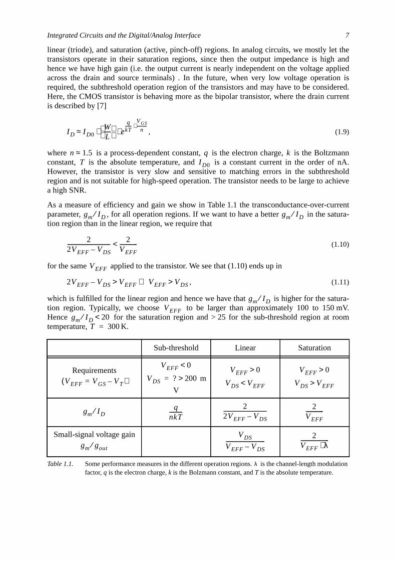
1 Introduction1.1 Some performance measures in the different operation regions. is the channel-length m
tion factor,q is the electron charge,k is the Bolzmann constant, andT is the absolute tempera-ture. 7
1.2 Specifics of different xDSL standards compared to voice channel techniques and ISDN.bandwidths are given by approximate numbers.
1.3 Spectral requirements on transmitted signal for ADSL at both CO and CPE sides.
2 Introduction to D/A Conversion2.1 Some digital codes used for D/A conversion.
3 D/A Converter Architectures3.1 Different digital interpolation filter orders for attenuation of images by more than 60 dB.3.2 Different continuous-time image-rejection filter orders for stop-band attenuation of 60 dB3.3 Reported performance of mainly telecommunication DACs.
4 Behavioral-Level Models for Current-Steering, Nyquist-Rate D/A Con-verters
5 Current-Steering D/A Converters5.1 Data summary of some implemented DACs. 1
6 Oversampling D/A Converters6.1 Feedback coefficients for different multi-feedback modulator orders for OSR=32.6.2 Achievable ENOB for different OSDAC configurations. 186.3 Interpolation filter orders for different structures and OSR. 16.4 Modulator feedback coefficients used in the OSDAC simulations.6.5 Semi-digital FIR filter orders for different OSR and stopband attenuation.
7 Special Techniques for Enhanced D/A Conversion7.1 Decision table for hardware efficient DEM. 20
8 Appendices
xiii

List of Tables xiv
ations.ally. Inrans-d up tof theoldmenet-
adio,tter isencyThe
ength,ssion
i.e.,s andks in a
on lin-
obilerd theards,m
theserter
ne orignaland
1 IntroductionThroughout the years there has been an increase of demand for high-speed communicDuring the last decades, the Internet and mobile terminal usage has increased dramaticour part of the world, they are now to a large extent every man’s property. The offered tmission data rate on ordinary telephone wires, i.e., voice-band modem, has been pusheapproximately 56 kbit/s. This achievable limit is basically set by the noise and linearity ochannel – the line quality –, but mostly by the limited bandwidth provided by the plaintelephone service (POTS), which typically is in the order of 3.1 to 5 kHz [1, 2]. To overcothis limited data rate, we can use dedicated wires with higher bandwidth, e.g., cable-TVwork, integrated service digital network (ISDN), ethernet, wireless access through rfibres, or a higher bandwidth on the available telephone wires has to be offered. The lathe concept of the digital subscriber line (DSL) standards. With filters we split the frequrange into the DC to 4-kHz band for POTS and the frequencies above 4 kHz for DSL.DSL standards allow data-rates up to several tens of Mbit/s [1, 2, 3] dependent on the lphysical dimensions, and quality of the line. The increase of bandwidth and transmispeed does not only put high demands on the quality of the telephone wire itself,crosstalk, noise, and interference. The interfacing circuits and front-ends in the modembase stations have to be very carefully designed and constructed. Some of the bottle-necDSL front-end are the analog circuits and the data converters, since the requirementsearity and low noise are very demanding [1, 2].
The same kind of problems with too low bandwidth have arosen for mobile terminals (mphones). In the common, established global system mobile telephony (GSM) standamaximum transmission data rate is approximately 9.6 kbit/s. New wideband radio stande.g., EDGE, UMTS, WCDMA, GPRS, will overcome the limitation, but still some of theonly allow rates up to 160 kbit/s [4].
This thesis overviews the interface between the digital and analog domains. Withininterfaces, we find the analog-to-digital converter (ADC) and digital-to-analog conve(DAC). These data converters are not only used for conversion of audio via micropholoudspeakers, video via camera or display, into information that the computer or digital sprocessor (DSP) can handle. In Fig. 1.1 we illustrate the concept of the interfacing ADC
1
2 Introduction
trans-, then sentgnal).cation
alsy largeant ale. The
tems.ll vol-small
ly in asrcon-h lesspossi-
due toOSMOSever,imple-rfor-s soon
tal-to-tions.and
z and, 3].very
erfor-whichd/or
DAC between the analog and digital domains. The data converters are also used for datamission via a channel, where the channel is either wireline or wireless (radio). Typicallydata (signal) is modulated onto a carrier according to some scheme. The signal is theover the channel with the carrier. The receiver will demodulate and extract the data (siThe modulation can be done in both the digital and analog domain dependent on appliand feasability.
A low power dissipation of the electronic circuits is very important, both in mobile terminto increase the stand-by time, but also in the base stations where the number of relativeland expensive cooling devices should be kept at a minimum. The newtork operators wsingle base station to be able to concurrently handle as many channels (users) as possibsame holds for the size of the modems (line cards) in the central office (CO) in DSL sysThis also implies that in both cases the circuits should be low-cost and occupy a smaume, hence the circuits should be highly integrated. Both issues, power dissipation andarea, are handled by integrating as much as possible in semi-conductors and preferabfew chips as possible. In this way, the off-chip communication is reduced, i.e., the intenection wires become much shorter and the power dissipation can be reduced througdriver circuits. Supply voltages can be shared, etc. To integrate as many components asble in as few chips as possible implies, today, that a CMOS technology should be usedits scalability and low-power operation [5]. In terms of linearity and low noise, the CMtechnology might not be the best choice for analog circuits, whereas the bipolar or BiCtechnology might be a better choice due to the higher gain of bipolar devices [7, 8]. Howmost of the research today on analog circuits is focused on CMOS, so that they can bemented together with digital circuits in a mixed-signal environment. There is a rapid pemance increase of the CMOS processes and the achievable unity-gain frequency iin the same order as for the bipolar transistors [8].
This thesis focuses on the study and design of – analysis and synthesis – of CMOS digianalog converters in analog front-ends (AFEs) for wideband and high-resolution applicaAs main target specifications, the asymmetric and very high data-rate DSL (ADSLVDSL) applications were chosen. The specified transmission bandwidths are 1.104 MH11.04 MHz, respectively, and the required resolution is in the order of 12-14 bits [1, 2(Actually, the specifications on the data converters in for example wideband radio aresimilar to those of the VDSL [4]).
We discuss models of the DACs which helps us understand the fundamental limits on pmance. The models are implemented in a higher-level language, such as Matlabincreases the flexibility (in terms of architecture modification and signal generation an
Figure 1.1 Data converters as interface between the analog and digital domain.
ADC
DAC
Digital Analog
f T( )
3
an beourse
or the
fer-resis-
ssed inn gen-hereTradi-may
l tech-1]. Thehavior
ack-irelinepecifi-
es ofance
plica--perfor-
ancelateds itselfmage-ency
ation.hapingise-erters
nce ofussedrs ofto in
e workions of
hap-D/AD/A
a 3.3-
analysis) over circuit-level languages, such as Spice or Spectre. The simulation time creduced from several days to a couple of minutes. The behavioral-level models are of cnot as detailed and accurate as the circuit-level models, but they give us a guideline fdesign.
Limits on the DAC performance are typically circuit noise, mismatch between internal reences or weights, nonlinear analog circuits, delay skew between switches, and parasitictance and capacitance [7, 9]. How these nonidealties affect the performance are addrethis thesis and we discuss different approaches to reduce the influence of the errors. Ieral, the errors or limitations can be considered to be of two types; static and dynamic, wthe former relates to signal-independent errors and the latter to signal-dependent errors.tional error reduction techniques focus on the static errors, for example, distortion termsbe averaged into signal-independent noise. In order to obtain high performance specianiques, such as spectral matching error shaping or inverse functions can be used [10, 1influence of dynamic errors must be treated in special ways and the analysis of their beis complex.
To illustrate some of the design complexities, we give in this introductory chapter a bground and an overview of the current research on data converters and especially for wcommunications. We also outline the requirements put on the data converters by DSL scations.
In Chapter 2 we give a more detailed description of D/A conversion in general. Propertiquantization noise, discrete-time signals, etc. are discussed. Different important performmeasures valid for telecommunications applications are also described.
In Chapter 3 the most common D/A converter architectures used in communications aptions are discussed and their properties are discussed and compared. Several highmance D/A converters found in literature and from data sheets are used in a performcomparison. Since the output of the D/A converter is mostly pulse amplitude modu(PAM), e.g., sample-and-held, the output spectrum becomes sinc weighted and repeatat multiples of the sample frequency. The images must be attenuated by analog filters (irejection filters) and to be able to use a lower filter order we cannot use the whole frequrange up to half the sampling frequency. This is referred to as oversampling or interpolSince we are using a higher sample frequency than required, we may also apply noise-sto effectively utilize the unused frequency space. We will refer to D/A converters with noshaping loops and oversampling as oversampling D/A converters (OSDACs) and to convwith oversampling only as interpolating D/A converters.
To assist the designer to understand some of the fundamental limitations on performaDACs, extensive models of the influence of different typical analog error sources is discin Chapter 4. For example, we show how limited output impedance and matching errounit DAC elements affect the linearity of the converter. These models are also referredfollowing chapters, where we compare measured, simulated, and calculated results. Thhas also yielded some closed formulas expressing some linearity measures as functparameters given by the error sources.
Chapter 5 and Chapter 6 discuss the circuit-level implementation of D/A converters. In Cter 5 we discuss the design of some 2.7-V to 5-V CMOS current-steering Nyquist-rateconverters. The nominal resolution is 10 through 14 bits. The design of oversamplingconverters with noise-shaping loops (OSDAC) is discussed in Chapter 6. The design of
4 Introduction
omes after
erfor-d but
binaryivitycom-
mise
hap-aterial
rtantlife-Intelnow-
rdingled
, lap-dense,ionshigh-ill in
chnol-
ce itthe
elop-ump-s theolt-
andsuchixed-
V to 5-V CMOS oversampling D/A converter is presented. The differences between sgenerations of converters are highlighted and we show the improved measured resultminor changes to the design.
In Chapter 7 we discuss the implementation of special techniques to further improve pmance of DACs. Especially dynamic element matching (DEM) techniques are considerealso other pre-distortion techniques to cancel specific DAC errors. In most cases thecode is not optimum in terms of performance, since it will give rise to glitches and sensitto matching errors. Instead the thermometer code is widely used. We show an interestingparison of the results when using several different input codes in the DAC. A comprobetween extremes is the proposed linear-coded approach.
Chapter 8 contains appendices with derivation of formulas throughout the thesis.
Some of the chapters are slighlty overlapping to simplify for the reader to focus a single cter rather than reading the whole thesis. The author’s publications are related to the mpresented in the thesis, and in the preface the disposition of those was presented.
1.1 Integrated Circuits and the Digital/Analog InterfaceThe invention or construction of the integrated circuit is probably one of the most impoinventions during the previous century. Its impact on modern communication and in factstyle is tremendous. The first large-scale integrated (LSI) circuit is considered to be the4004 microprocessor. It was delivered in 1971 and contained about 2300 transistors andadays (Jan. 2001), the largest chips contain several tens of millions of transistors. Accoto the so calledMoore’s law, the density of transistors on a chip is approximately doubevery 18th month.
In this information technology era, products such as wireless terminals (mobile phones)top computers, bluetooth modules, and personal digital assistants (PDAs), require fast,and low power consuming integrated circuits. For high-integration, low-power applicatthe bipolar technique has been replaced by the CMOS technique. However, still for veryspeed and high-performance applications the bipolar technique is widely used [5]. We wour case consider the CMOS technology throughout the thesis and leave the bipolar teogy for now.
In general, we want to implement both analog and digital circuits on the same chip, sinreduces the off-chip design complexity, e.g. layout of printed circuit board (PCB), andinduced disturbance on sensitive interconnection wires is reduced. With the rapid devment of digital circuits, the supply voltage is decreasing which reduces the power constion. For the analog side, the design of high-efficiency circuits becomes complicated avoltage range is shrinking. Future design of analog circuits will most likely focus on low-vage operation and maybe even subthreshold operation.
A mixed-signal circuit is more or less considered to be a subcircuit in which both analogdigital circuits are used. Typically, the interface between the digital and analog domain,as the D/A or A/D converter, as well as phase-locked loops (PLL) are considered to be msignal circuits.
Integrated Circuits and the Digital/Analog Interface 5
dentasings very
f bitspower
racy.t at a
aci-s the
on-
nde toepen-d and
ors asowers we
can beethod
nd onecon-
ut iss the
nstant.loadinter-more
1.1.1 Digital CircuitsThe design of digital circuits can be divided into a number of different disciplines. Depenon application, either one of the disciplines become more or less important. With decretransistor dimensions, the influence of wire lengths, parasitic capacitance, etc., becomeimportant and in some sense this requires knowledge in pure analog design as well.
The accuracy of the circuit is increased by simply increasing the word length (number oused to represent the signals) to a desired level. This increases the chip area and thedissipation, which in an actual implementation probably set the upper limit on the accuWith carefully evaluated algorithms and long word lengths the digital noise can be kepvery low level.
For a digital CMOS circuit, the power dissipation is approximately [5]
, (1.1)
where is the circuit’s switching activity, is the clock frequency, is the average captive load for each gate, is the number of gates, is the supply voltage, and iswing. The speed is inversely proportional to the time constant where is theresistance of the CMOS transistor approximately [7] given by
, (1.2)
where is a process-dependent parameter, is the transistor size aspect ratio, ais the threshold voltage. Although it affects the speed of the circuit, it is a natural choicreduce the supply voltage in order to lower the power dissipation due to the quadratic ddency in (1.1). By reducing the average load capacitance we gain in both higher speelower power consumption. This is done by using as short wires and as small transistpossible. We also find the obvious conclusion that with fewer gates, , we get a lower pconsumption. Therefore, the algorithms are very important, since with good algorithmcan reduce the number of gates as well.
As measures on performance the maximum speed, power dissipation, chip area, etc.,used to characterize and compare digital circuits. But a general, good comparison mdoes not exist. However, the achievable speed is dependent on the supply voltage aalternative performance measure is the power delay product (PDP) [5], which basicallysiders both (1.1) and (1.2) but is defined as
, (1.3)
where is the propagation time. This may not be equal to the time constant bin the same order of magnitude. Using (1.1) in (1.3) and assuming full-scale swings giveapproximate PDP
, (1.4)
where is a constant given by the ratio between the propagation speed and the time coWe find that the PDP approximately is linearly dependent on the supply voltage. Thecapacitance is determined by the following number of transistor gates and length of theconnection wires. Today, with shrinking dimensions, the wire capacitance is becoming
P αf CL VDD n ∆V⋅ ⋅ ⋅ ⋅≈
α f CLn VDD ∆V
RonCL Ron
Ron K' W L⁄( ) VDD VT–( )⋅ ⋅[ ] 1–≈
K' W L⁄ VT
n
PDP P τP⋅=
τP RonCL( )
PDP kαf CL
2VDD
2n⋅ ⋅ ⋅
K' W L⁄( ) VDD VT–( )⋅ ⋅-------------------------------------------------------------⋅≈
k
6 Introduction
o, trueniques
workmanceal cir-ed or
there-
is thediffi-itingnents.
ircuitimi-ower
ifica-
ircuit.
pen-
and
argin,
hold,
important than the number of gates [6].
To increase speed and throughput, special logic styles such as precharged logic, dominsingle-phase clocking (TSPC), etc., are used [12]. There are also special adiabatic techused to reduce power dissipation [6].
1.1.2 Analog CircuitsThere are automated tools for layout and design of analog circuits, but still much of thehas to be done by hand. An experienced designer is needed to implement high-perforanalog circuits. Due to short-channel effects, analog circuits do not scale as well as digitcuits. We mostly have to completely redesign our circuit when the process is changupdated. However, smaller process dimensions also give less parasitic capacitance andfore the achievable bandwidth can be increased, etc.
For analog designers, one of the major problems with modern CMOS technologiesdecreasing supply voltage. A low supply voltage slows down the circuits [8]. It becomescult to design for example a current source with high output impedance which is one limfactor on performance. Some other important design issues is the matching of compoVery careful layout has to be used to reach good matching.
When analyzing and designing analog circuits we consider the linearization of the caround the operating point. Unlike digital circuits, analog circuits, such as amplifiers or slar, are typically biased to a certain voltage level with a DC bias current. Therefore, the pdissipation is given by the bias current times the supply voltage.
. (1.5)
The bias current is typically set by a slew rate (SR) specification (or by the power spection, etc.), where we may have
, (1.6)
where is the load capacitance. The speed is given by the bandwidth of the analog cFor an amplifier in a feedback configuration, we have
, (1.7)
where is the feedback factor and is the unity-gain frequency of the amplifier in oloop configuration. Approximately, we have that
, (1.8)
where is the small-signal transconductance of the amplifier. Typically,hence for smaller voltage levels we get a poor and thereby a slow amplifier.
As measures on accuracy and performance we consider for example, DC gain, phase mbandwidth, distortion, noise, power dissipation, slew rate, common-mode rejection, etc.
The CMOS transistor operates in a number of different regions, the cut-off or subthres
P Ibias VDD⋅=
SRI bias
CL----------≥
CL
τg1
β ωu⋅--------------=
β ωu
τg
CL
β gm⋅--------------=
gm gm VGS VT–∼gm
Integrated Circuits and the Digital/Analog Interface 7
t theh andppliedion isidered.urrent
mannf nA.
sholdchieve
urrenttura-
ura-mV.oom
lation
linear (triode), and saturation (active, pinch-off) regions. In analog circuits, we mostly letransistors operate in their saturation regions, since then the output impedance is highence we have high gain (i.e. the output current is nearly independent on the voltage aacross the drain and source terminals) . In the future, when very low voltage operatrequired, the subthreshold operation region of the transistors and may have to be consHere, the CMOS transistor is behaving more as the bipolar transistor, where the drain cis described by [7]
, (1.9)
where is a process-dependent constant, is the electron charge, is the Boltzconstant, is the absolute temperature, and is a constant current in the order oHowever, the transistor is very slow and sensitive to matching errors in the subthreregion and is not suitable for high-speed operation. The transistor needs to be large to aa high SNR.
As a measure of efficiency and gain we show in Table 1.1 the transconductance-over-cparameter, , for all operation regions. If we want to have a better in the sation region than in the linear region, we require that
(1.10)
for the same applied to the transistor. We see that (1.10) ends up in
, (1.11)
which is fulfilled for the linear region and hence we have that is higher for the sattion region. Typically, we choose to be larger than approximately 100 to 150Hence for the saturation region and > 25 for the sub-threshold region at rtemperature, K.
Sub-threshold Linear Saturation
Requirementsm
V
Small-signal voltage gain
Table 1.1. Some performance measures in the different operation regions. is the channel-length modufactor,q is the electron charge,k is the Bolzmann constant, andT is the absolute temperature.
I D I D0WL-----
eq
kT------
VGS
n----------⋅
⋅ ⋅≈
n 1.5≈ q kT ID0
gm I D⁄ gm I D⁄
22VEFF VDS–-------------------------------- 2
VEFF-------------<
VEFF
2VEFF VDS– VEFF> VEFF VDS>⇒
gm I D⁄VEFF
gm I D⁄ 20<T 300=
VEFF VGS VT–=( )
VEFF 0<
VDS ? 200>=VEFF 0>
VDS VEFF<
VEFF 0>
VDS VEFF>
gm I D⁄ qnkT----------
22VEFF VDS–-------------------------------- 2
VEFF-------------
gm gout⁄VDS
VEFF VDS–-----------------------------
2VEFF λ⋅---------------------
λ
8 Introduction
iderfunc-
er thecuits.
agestrategitales aresidersamee digi-sub-rough, weoise,
ntacts,
andputa-implewhat
d the
ciallyis to
gener-e and, cop-
the
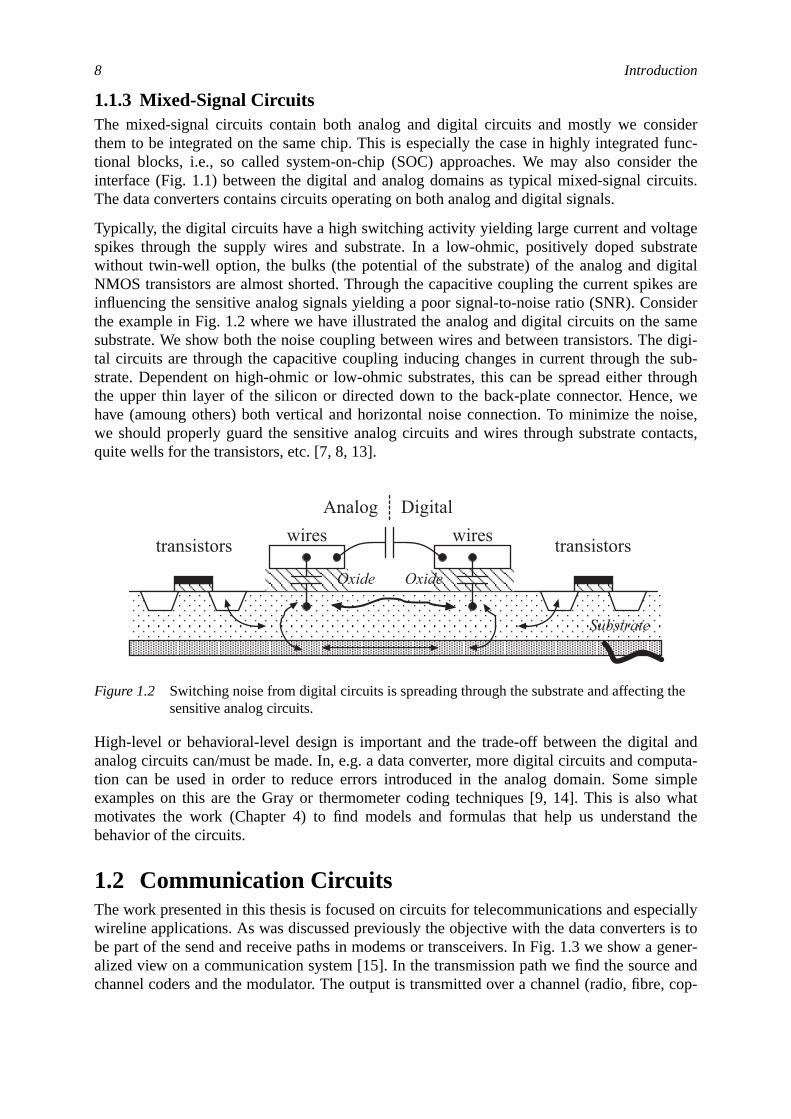
1.1.3 Mixed-Signal CircuitsThe mixed-signal circuits contain both analog and digital circuits and mostly we consthem to be integrated on the same chip. This is especially the case in highly integratedtional blocks, i.e., so called system-on-chip (SOC) approaches. We may also considinterface (Fig. 1.1) between the digital and analog domains as typical mixed-signal cirThe data converters contains circuits operating on both analog and digital signals.
Typically, the digital circuits have a high switching activity yielding large current and voltspikes through the supply wires and substrate. In a low-ohmic, positively doped subwithout twin-well option, the bulks (the potential of the substrate) of the analog and diNMOS transistors are almost shorted. Through the capacitive coupling the current spikinfluencing the sensitive analog signals yielding a poor signal-to-noise ratio (SNR). Conthe example in Fig. 1.2 where we have illustrated the analog and digital circuits on thesubstrate. We show both the noise coupling between wires and between transistors. Thtal circuits are through the capacitive coupling inducing changes in current through thestrate. Dependent on high-ohmic or low-ohmic substrates, this can be spread either ththe upper thin layer of the silicon or directed down to the back-plate connector. Hencehave (amoung others) both vertical and horizontal noise connection. To minimize the nwe should properly guard the sensitive analog circuits and wires through substrate coquite wells for the transistors, etc. [7, 8, 13].
High-level or behavioral-level design is important and the trade-off between the digitalanalog circuits can/must be made. In, e.g. a data converter, more digital circuits and comtion can be used in order to reduce errors introduced in the analog domain. Some sexamples on this are the Gray or thermometer coding techniques [9, 14]. This is alsomotivates the work (Chapter 4) to find models and formulas that help us understanbehavior of the circuits.
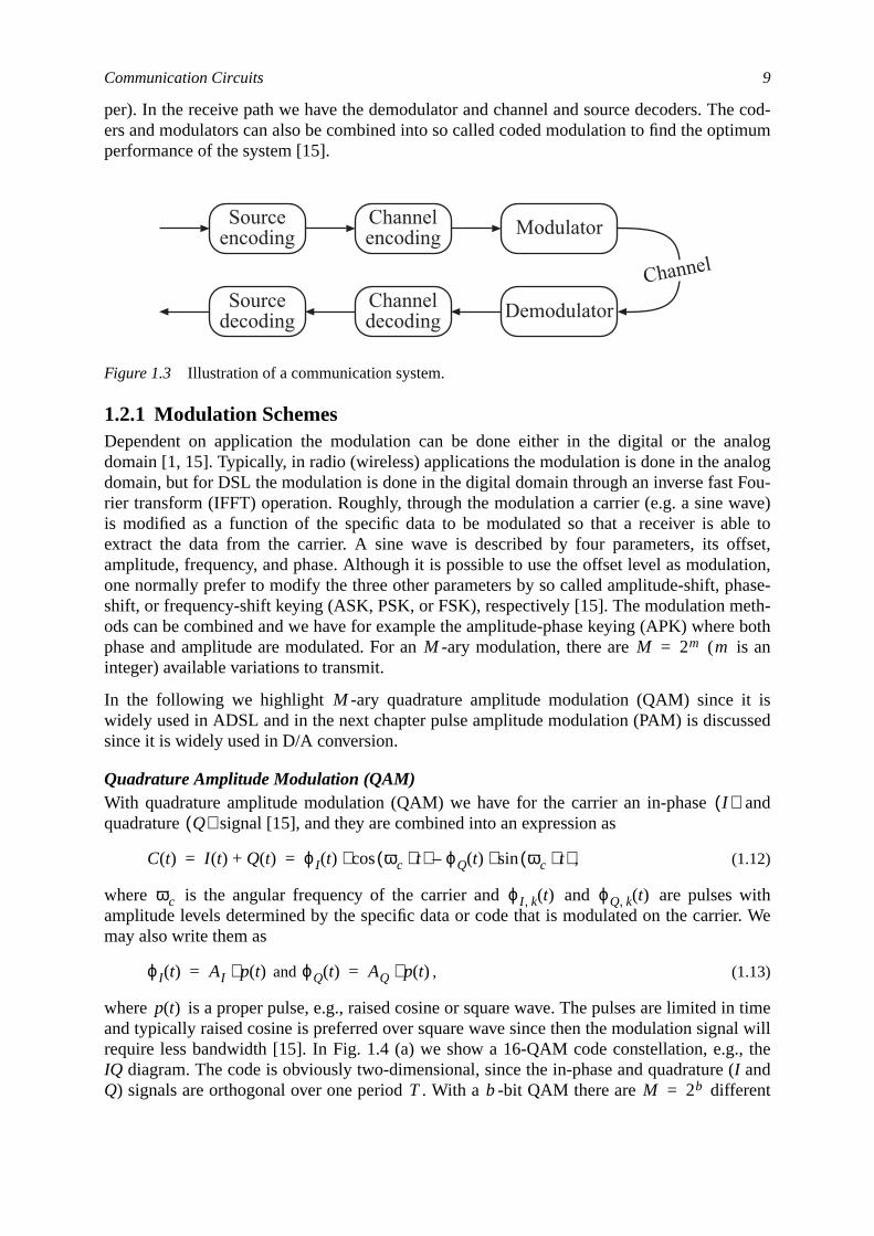
1.2 Communication CircuitsThe work presented in this thesis is focused on circuits for telecommunications and espewireline applications. As was discussed previously the objective with the data convertersbe part of the send and receive paths in modems or transceivers. In Fig. 1.3 we show aalized view on a communication system [15]. In the transmission path we find the sourcchannel coders and the modulator. The output is transmitted over a channel (radio, fibre
Figure 1.2 Switching noise from digital circuits is spreading through the substrate and affectingsensitive analog circuits.
wires
Substrate
Oxide Oxide
transistors wires transistors
Analog Digital
Communication Circuits 9
he cod-timum
nalogalogFou-ave)
ble toffset,
lation,hase-th-
e bothis an
isssed
and
withr. We
in timeal will, the(ent
per). In the receive path we have the demodulator and channel and source decoders. Ters and modulators can also be combined into so called coded modulation to find the opperformance of the system [15].
1.2.1 Modulation SchemesDependent on application the modulation can be done either in the digital or the adomain [1, 15]. Typically, in radio (wireless) applications the modulation is done in the andomain, but for DSL the modulation is done in the digital domain through an inverse fastrier transform (IFFT) operation. Roughly, through the modulation a carrier (e.g. a sine wis modified as a function of the specific data to be modulated so that a receiver is aextract the data from the carrier. A sine wave is described by four parameters, its oamplitude, frequency, and phase. Although it is possible to use the offset level as moduone normally prefer to modify the three other parameters by so called amplitude-shift, pshift, or frequency-shift keying (ASK, PSK, or FSK), respectively [15]. The modulation meods can be combined and we have for example the amplitude-phase keying (APK) wherphase and amplitude are modulated. For an -ary modulation, there are (integer) available variations to transmit.
In the following we highlight -ary quadrature amplitude modulation (QAM) since itwidely used in ADSL and in the next chapter pulse amplitude modulation (PAM) is discusince it is widely used in D/A conversion.
Quadrature Amplitude Modulation (QAM)With quadrature amplitude modulation (QAM) we have for the carrier an in-phasequadrature signal [15], and they are combined into an expression as
, (1.12)
where is the angular frequency of the carrier and and are pulsesamplitude levels determined by the specific data or code that is modulated on the carriemay also write them as
and , (1.13)
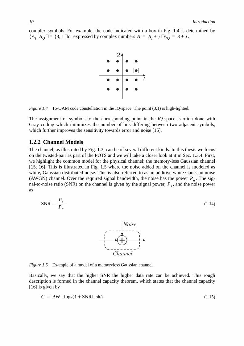
where is a proper pulse, e.g., raised cosine or square wave. The pulses are limitedand typically raised cosine is preferred over square wave since then the modulation signrequire less bandwidth [15]. In Fig. 1.4 (a) we show a 16-QAM code constellation, e.g.IQ diagram. The code is obviously two-dimensional, since the in-phase and quadratureI andQ) signals are orthogonal over one period . With a -bit QAM there are differ
Figure 1.3 Illustration of a communication system.
Channel
Sourceencoding
Channelencoding
Channeldecoding Demodulator
Modulator
Sourcedecoding
M M 2m= m
M
I( )Q( )
C t( ) I t( ) Q t( )+ ϕI t( ) ωc t⋅( )cos⋅ ϕQ t( ) ωc t⋅( )sin⋅–= =
ωc ϕI k, t( ) ϕQ k, t( )
ϕI t( ) AI p t( )⋅= ϕQ t( ) AQ p t( )⋅=
p t( )
T b M 2b=
10 Introduction
d by
ols,
focusFirst,anneled asnoisesig-
ower
roughpacity
complex symbols. For example, the code indicated with a box in Fig. 1.4 is determine or expressed by complex numbers .
The assignment of symbols to the corresponding point in theIQ-space is often done withGray coding which minimizes the number of bits differing between two adjacent symbwhich further improves the sensitivity towards error and noise [15].
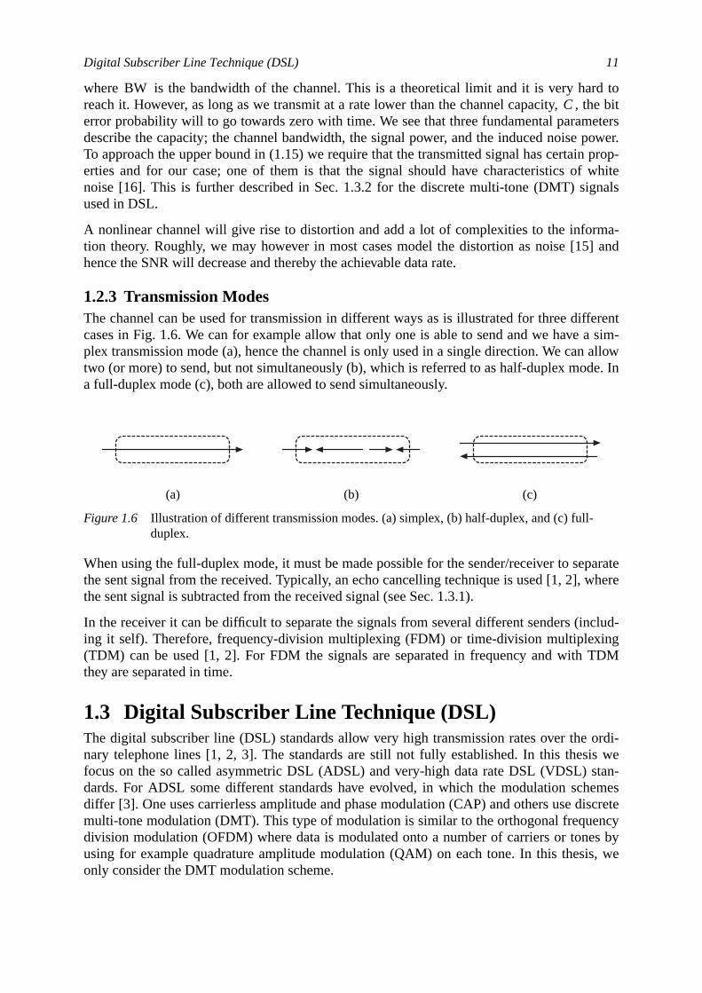
1.2.2 Channel ModelsThe channel, as illustrated by Fig. 1.3, can be of several different kinds. In this thesis weon the twisted-pair as part of the POTS and we will take a closer look at it in Sec. 1.3.4.we highlight the common model for the physical channel; the memory-less Gaussian ch[15, 16]. This is illustrated in Fig. 1.5 where the noise added on the channel is modelwhite, Gaussian distributed noise. This is also referred to as an additive white Gaussian(AWGN) channel. Over the required signal bandwidth, the noise has the power . Thenal-to-noise ratio (SNR) on the channel is given by the signal power, , and the noise pas
. (1.14)
Basically, we say that the higher SNR the higher data rate can be achieved. Thisdescription is formed in the channel capacity theorem, which states that the channel ca[16] is given by
bit/s, (1.15)
Figure 1.4 16-QAM code constellation in the IQ-space. The point (3,1) is high-lighted.
Figure 1.5 Example of a model of a memoryless Gaussian channel.
AI AQ,( ) 3 1,( )= A AI j AQ⋅+ 3 j+= =
Q
I
PnPs
SNRPs
Pn------=
Channel
Noise
C BW 1 SNR+( )log2⋅=
Digital Subscriber Line Technique (DSL) 11
d tothe biteterspower.prop-whitenals
a-] and
erenta sim-allowe. In
paratehere
clud-gDM
ordi-is wetan-emesiscretencys by, we
where is the bandwidth of the channel. This is a theoretical limit and it is very harreach it. However, as long as we transmit at a rate lower than the channel capacity, ,error probability will to go towards zero with time. We see that three fundamental paramdescribe the capacity; the channel bandwidth, the signal power, and the induced noiseTo approach the upper bound in (1.15) we require that the transmitted signal has certainerties and for our case; one of them is that the signal should have characteristics ofnoise [16]. This is further described in Sec. 1.3.2 for the discrete multi-tone (DMT) sigused in DSL.
A nonlinear channel will give rise to distortion and add a lot of complexities to the informtion theory. Roughly, we may however in most cases model the distortion as noise [15hence the SNR will decrease and thereby the achievable data rate.
1.2.3 Transmission ModesThe channel can be used for transmission in different ways as is illustrated for three diffcases in Fig. 1.6. We can for example allow that only one is able to send and we haveplex transmission mode (a), hence the channel is only used in a single direction. We cantwo (or more) to send, but not simultaneously (b), which is referred to as half-duplex moda full-duplex mode (c), both are allowed to send simultaneously.
When using the full-duplex mode, it must be made possible for the sender/receiver to sethe sent signal from the received. Typically, an echo cancelling technique is used [1, 2], wthe sent signal is subtracted from the received signal (see Sec. 1.3.1).
In the receiver it can be difficult to separate the signals from several different senders (ining it self). Therefore, frequency-division multiplexing (FDM) or time-division multiplexin(TDM) can be used [1, 2]. For FDM the signals are separated in frequency and with Tthey are separated in time.
1.3 Digital Subscriber Line Technique (DSL)The digital subscriber line (DSL) standards allow very high transmission rates over thenary telephone lines [1, 2, 3]. The standards are still not fully established. In this thesfocus on the so called asymmetric DSL (ADSL) and very-high data rate DSL (VDSL) sdards. For ADSL some different standards have evolved, in which the modulation schdiffer [3]. One uses carrierless amplitude and phase modulation (CAP) and others use dmulti-tone modulation (DMT). This type of modulation is similar to the orthogonal frequedivision modulation (OFDM) where data is modulated onto a number of carriers or toneusing for example quadrature amplitude modulation (QAM) on each tone. In this thesisonly consider the DMT modulation scheme.
(a) (b) (c)
Figure 1.6 Illustration of different transmission modes. (a) simplex, (b) half-duplex, and (c) full-duplex.
BWC
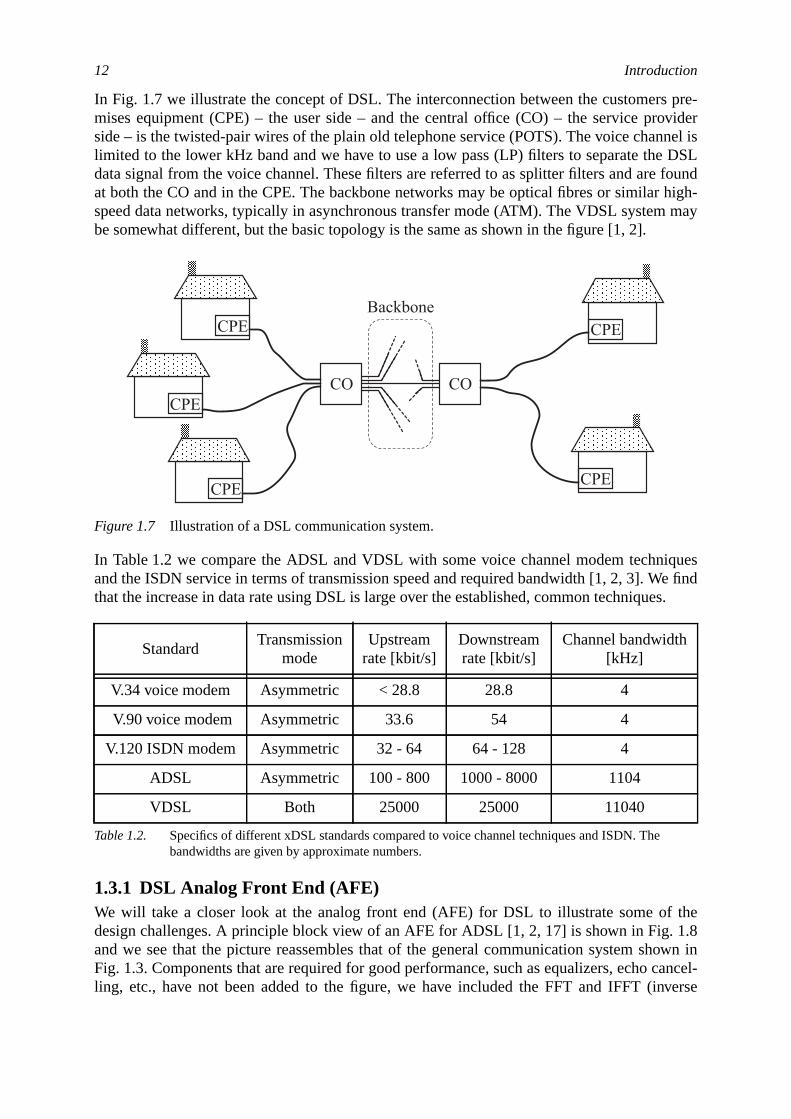
12 Introduction
pre-ovidernel isDSLfoundhigh-may
iquese findes.
the1.8own incancel-verse
In Fig. 1.7 we illustrate the concept of DSL. The interconnection between the customersmises equipment (CPE) – the user side – and the central office (CO) – the service prside – is the twisted-pair wires of the plain old telephone service (POTS). The voice chanlimited to the lower kHz band and we have to use a low pass (LP) filters to separate thedata signal from the voice channel. These filters are referred to as splitter filters and areat both the CO and in the CPE. The backbone networks may be optical fibres or similarspeed data networks, typically in asynchronous transfer mode (ATM). The VDSL systembe somewhat different, but the basic topology is the same as shown in the figure [1, 2].
In Table 1.2 we compare the ADSL and VDSL with some voice channel modem technand the ISDN service in terms of transmission speed and required bandwidth [1, 2, 3]. Wthat the increase in data rate using DSL is large over the established, common techniqu
1.3.1 DSL Analog Front End (AFE)We will take a closer look at the analog front end (AFE) for DSL to illustrate some ofdesign challenges. A principle block view of an AFE for ADSL [1, 2, 17] is shown in Fig.and we see that the picture reassembles that of the general communication system shFig. 1.3. Components that are required for good performance, such as equalizers, echoling, etc., have not been added to the figure, we have included the FFT and IFFT (in
Figure 1.7 Illustration of a DSL communication system.
StandardTransmission
modeUpstream
rate [kbit/s]Downstreamrate [kbit/s]
Channel bandwidth[kHz]
V.34 voice modem Asymmetric < 28.8 28.8 4
V.90 voice modem Asymmetric 33.6 54 4
V.120 ISDN modem Asymmetric 32 - 64 64 - 128 4
ADSL Asymmetric 100 - 800 1000 - 8000 1104
VDSL Both 25000 25000 11040
Table 1.2. Specifics of different xDSL standards compared to voice channel techniques and ISDN. Thebandwidths are given by approximate numbers.
CPE
CPE
CPE
CO CO
CPE
CPE
Backbone
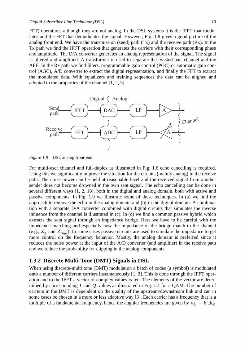
Digital Subscriber Line Technique (DSL) 13
odu-of theIn thephasesignald thecon-ractd and
ired.eivenotherone inandd thebina-ersehichith theannelto get
ce itpath
latedoper-deter-er ofan inthat is a
FFT) operations although they are not analog. In the DSL systems it is the IFFT that mlates and the FFT that demodulates the signal. However, Fig. 1.8 gives a good pictureanalog front end. We have the transmission (send) path (Tx) and the receive path (Rx).Tx path we find the IFFT operation that generates the carriers with their correspondingand amplitude. The D/A converter generates an analog representation of the signal. Theis filtered and amplified. A transformer is used to separate the twisted-pair channel anAFE. In the Rx path we find filters, programmable gain control (PGC) or automatic gaintrol (AGC), A/D converter to extract the digital representation, and finally the FFT to extthe modulated data. With equalizers and training sequences the data can be aligneadopted to the properties of the channel [1, 2, 3].
For multi-user channel and full-duplex as illustrated in Fig. 1.6 echo cancelling is requUsing this we significantly improve the situation for the circuits (mainly analog) in the recpath. The noise power can be held at reasonable level and the received signal from asender does not become drowned in the own sent signal. The echo cancelling can be dseveral different ways [1, 2, 18], both in the digital and analog domain, both with activepassive components. In Fig. 1.9 we illustrate some of these techniques. In (a) we finapproach to remove the echo in the analog domain and (b) in the digital domain. A comtion with a separate D/A converter combined with digital circuits that simulates the invinfluence from the channel is illustrated in (c). In (d) we find a common passive hybrid wextracts the sent signal through an impedance bridge. Here we have to be careful wimpedance matching and especially how the impedance of the bridge match to the ch(e.g., and ). In some cases passive circuits are used to simulate the impedancemore control on the frequency behavior. Mostly, the analog domain is preferred sinreduces the noise power at the input of the A/D converter (and amplifier) in the receiveand we reduce the probability for clipping in the analog components.
1.3.2 Discrete Multi-Tone (DMT) Signals in DSLWhen using discrete-multi tone (DMT) modulation a batch of codes (a symbol) is moduonto a number of different carriers instantaneously [1, 2]. This is done through the IFFTation and to the IFFT a vector of complex values is fed. The elements of the vector aremined by corresponding and values as illustrated in Fig. 1.4 for a QAM. The numbcarriers in the DMT is dependent on the quality of the upstream/downstream link and csome cases be chosen in a more or less adaptive way [3]. Each carrier has a frequencymultiple of a fundamental frequency, hence the angular frequencies are given by
Figure 1.8 DSL analog front-end.
Channel
IFFT DAC LP A
FFT ADC LP A
Digital Analog
Sendpath
Receivepath
Z3 Zline
I Q
ωc k ω0⋅=
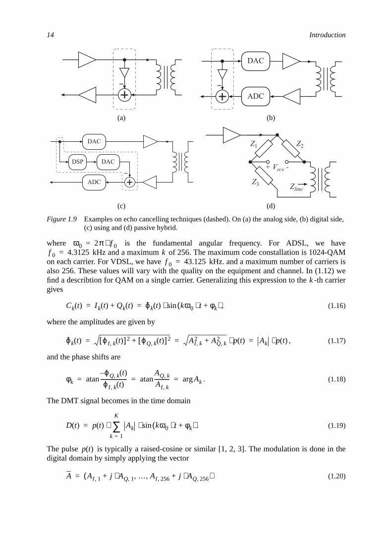
14 Introduction
aveAMrs is) werrier
the
l side,
where is the fundamental angular frequency. For ADSL, we hkHz and a maximum of 256. The maximum code constallation is 1024-Q
on each carrier. For VDSL, we have kHz. and a maximum number of carriealso 256. These values will vary with the quality on the equipment and channel. In (1.12find a describtion for QAM on a single carrier. Generalizing this expression to the -th cagives
, (1.16)
where the amplitudes are given by
, (1.17)
and the phase shifts are
. (1.18)
The DMT signal becomes in the time domain
. (1.19)
The pulse is typically a raised-cosine or similar [1, 2, 3]. The modulation is done indigital domain by simply applying the vector
(1.20)
(a) (b)
(c) (d)
Figure 1.9 Examples on echo cancelling techniques (dashed). On (a) the analog side, (b) digita(c) using and (d) passive hybrid.
DAC
ADC
DAC
ADC
DACDSP
Z1 Z2
Z3 Zline
+ Vrcv -
ω0 2π f 0⋅=f 0 4.3125= k
f 0 43.125=
k
Ck t( ) I k t( ) Qk t( )+ ϕk t( ) kω0 t⋅ φk+( )sin⋅= =
ϕk t( ) ϕI k, t( )[ ]2 ϕQ k, t( )[ ]2+ AI k,2 AQ k,
2+ p t( )⋅ Ak p t( )⋅= = =
φk
ϕQ k, t( )–
ϕI k, t( )--------------------atan
AQ k,AI k,-----------atan Akarg= = =
D t( ) p t( ) Ak kω0 t⋅ φk+( )sin⋅k 1=
K
∑⋅=
p t( )
A AI 1, j AQ 1,⋅+ … AI 256, j AQ 256,⋅+, ,( )=
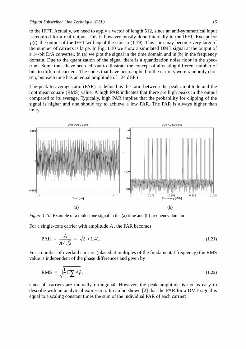
Digital Subscriber Line Technique (DSL) 15
inputt fore ifut ofncy
spec-er of
y cho-
nd theutputthethan
RMS
sy toal is
to the IFFT. Actually, we need to apply a vector of length 512, since an anti-symmetricalis required for a real output. This is however mostly done internally in the IFFT. Excep
the output of the IFFT will equal the sum in (1.19). This sum may become very largthe number of carriers is large. In Fig. 1.10 we show a simulated DMT signal at the outpa 14-bit D/A converter. In (a) we plot the signal in the time domain and in (b) in the frequedomain. Due to the quantization of the signal there is a quantization noise floor in thetrum. Some tones have been left out to illustrate the concept of allocating different numbbits to different carriers. The codes that have been applied to the carriers were randomlsen, but each tone has an equal amplitude of –24 dBFS.
The peak-to-average ratio (PAR) is defined as the ratio between the peak amplitude aroot mean square (RMS) value. A high PAR indicates that there are high peaks in the ocompared to its average. Typically, high PAR implies that the probability for clipping ofsignal is higher and one should try to achieve a low PAR. The PAR is always higherunity.
For a single-tone carrier with amplitude , the PAR becomes
. (1.21)
For a number of overlaid carriers (placed at multiples of the fundamental frequency) thevalue is independent of the phase differences and given by
, (1.22)
since all carriers are mutually orthogonal. However, the peak amplitude is not as eadescribe with an analytical expression. It can be shown [2] that the PAR for a DMT signequal to a scaling constant times the sum of the individual PAR of each carrier:
(a) (b)
Figure 1.10 Example of a multi-tone signal in the (a) time and (b) frequency domain
p t( )
3 4
−8192
0
8192
DMT ADSL signal
Time [ms]0 0.276 0.552 0.828 1.104
−140
−100
−24
−6
DMT ADSL signalP
ower
[dB
FS
]
Frequency [MHz]
A
PAR A
A 2⁄--------------- 2 1.41≈= =
RMS12--- Ak
2∑⋅=
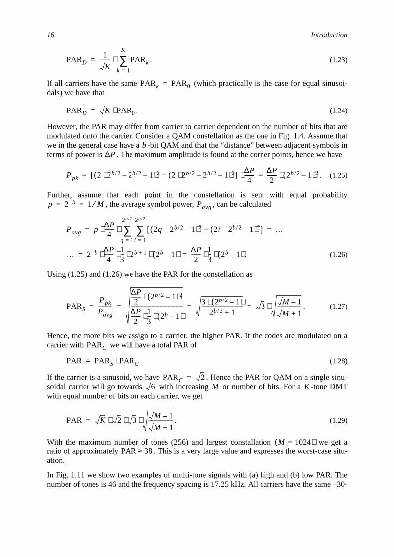
16 Introduction
soi-
t aree thatols in
have
bility
d on a
inu-T
et asitu-
Thee –30-
. (1.23)
If all carriers have the same (which practically is the case for equal sinudals) we have that
. (1.24)
However, the PAR may differ from carrier to carrier dependent on the number of bits thamodulated onto the carrier. Consider a QAM constellation as the one in Fig. 1.4. Assumwe in the general case have a -bit QAM and that the “distance” between adjacent symbterms of power is . The maximum amplitude is found at the corner points, hence we
. (1.25)
Further, assume that each point in the constellation is sent with equal proba, the average symbol power, , can be calculated
. (1.26)
Using (1.25) and (1.26) we have the PAR for the constellation as
. (1.27)
Hence, the more bits we assign to a carrier, the higher PAR. If the codes are modulatecarrier with we will have a total PAR of
. (1.28)
If the carrier is a sinusoid, we have . Hence the PAR for QAM on a single ssoidal carrier will go towards with increasing or number of bits. For a -tone DMwith equal number of bits on each carrier, we get
. (1.29)
With the maximum number of tones (256) and largest constallation we gratio of approximately . This is a very large value and expresses the worst-caseation.
In Fig. 1.11 we show two examples of multi-tone signals with (a) high and (b) low PAR.number of tones is 46 and the frequency spacing is 17.25 kHz. All carriers have the sam
PARD1
K-------- PARk
k 1=
K
∑⋅=
PARk PAR0=
PARD K PAR0⋅=
b∆P
Ppk 2 2b 2/⋅ 2b 2/– 1–( )2 2 2b 2/⋅ 2b 2/– 1–( )2+[ ] ∆P4
-------⋅ ∆P2
------- 2b 2/ 1–( )2⋅= =
p 2 b– 1 M⁄= = Pavg
Pavg p∆P4
-------⋅ 2q 2b 2/– 1–( )2 2i 2b 2/– 1–( )2+[ ]i 1=
2b 2/
∑q 1=
2b 2/
∑⋅ …= =
… 2 b– ∆P4
-------⋅ 13--- 2b 1+ 2b 1–( )⋅ ⋅ ⋅ ∆P
2------- 1
3--- 2b 1–( )⋅ ⋅= =
PARS
Ppk
Pavg----------
∆P2
------- 2b 2/ 1–( )2⋅
∆P2
------- 13--- 2b 1–( )⋅ ⋅
--------------------------------------- 3 2b 2/ 1–( )⋅2b 2/ 1+
------------------------------- 3 M 1–
M 1+------------------⋅= = = =
PARC
PAR PARS PARC⋅=
PARC 2=6 M K
PAR K 2 3 M 1–
M 1+------------------⋅ ⋅ ⋅=
M 1024=( )PAR 38≈
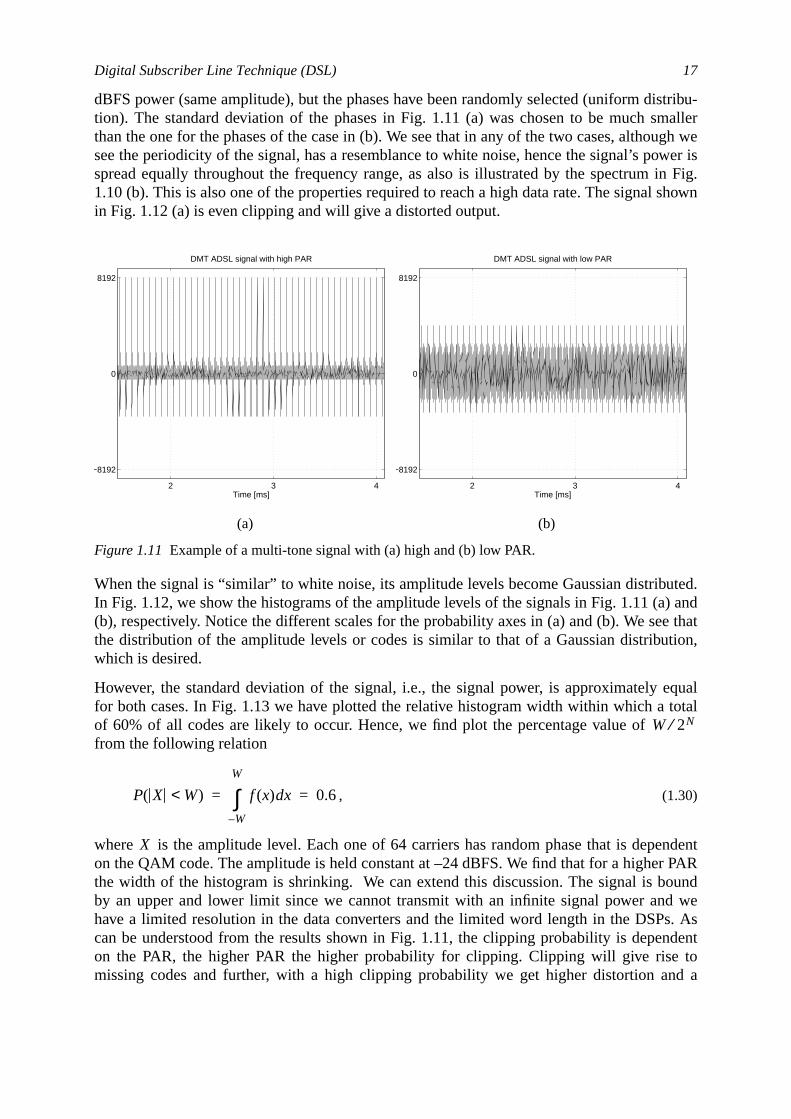
Digital Subscriber Line Technique (DSL) 17
istribu-mallerugh wewer is
in Fig.shown
uted.) ande thattion,
equaltotal
endentPARound
wes. Asdenttod a
dBFS power (same amplitude), but the phases have been randomly selected (uniform dtion). The standard deviation of the phases in Fig. 1.11 (a) was chosen to be much sthan the one for the phases of the case in (b). We see that in any of the two cases, althosee the periodicity of the signal, has a resemblance to white noise, hence the signal’s pospread equally throughout the frequency range, as also is illustrated by the spectrum1.10 (b). This is also one of the properties required to reach a high data rate. The signalin Fig. 1.12 (a) is even clipping and will give a distorted output.
When the signal is “similar” to white noise, its amplitude levels become Gaussian distribIn Fig. 1.12, we show the histograms of the amplitude levels of the signals in Fig. 1.11 (a(b), respectively. Notice the different scales for the probability axes in (a) and (b). We sethe distribution of the amplitude levels or codes is similar to that of a Gaussian distribuwhich is desired.
However, the standard deviation of the signal, i.e., the signal power, is approximatelyfor both cases. In Fig. 1.13 we have plotted the relative histogram width within which aof 60% of all codes are likely to occur. Hence, we find plot the percentage value offrom the following relation
, (1.30)
where is the amplitude level. Each one of 64 carriers has random phase that is depon the QAM code. The amplitude is held constant at –24 dBFS. We find that for a higherthe width of the histogram is shrinking. We can extend this discussion. The signal is bby an upper and lower limit since we cannot transmit with an infinite signal power andhave a limited resolution in the data converters and the limited word length in the DSPcan be understood from the results shown in Fig. 1.11, the clipping probability is depenon the PAR, the higher PAR the higher probability for clipping. Clipping will give risemissing codes and further, with a high clipping probability we get higher distortion an
(a) (b)
Figure 1.11 Example of a multi-tone signal with (a) high and (b) low PAR.
2 3 4
−8192
0
8192
DMT ADSL signal with high PAR
Time [ms]2 3 4
−8192
0
8192
DMT ADSL signal with low PAR
Time [ms]
W 2N⁄
P X W<( ) f x( ) xd
W–
W
∫ 0.6= =
X
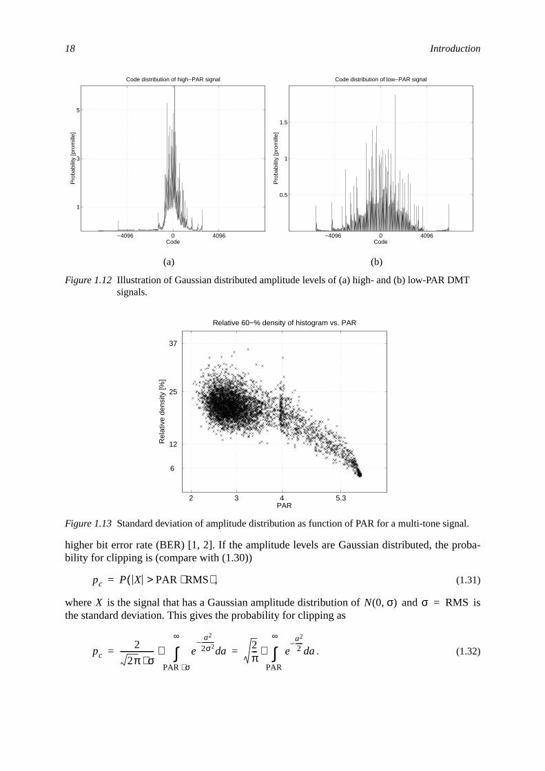
18 Introduction
oba-
is
T
l.
higher bit error rate (BER) [1, 2]. If the amplitude levels are Gaussian distributed, the prbility for clipping is (compare with (1.30))
, (1.31)
where is the signal that has a Gaussian amplitude distribution of andthe standard deviation. This gives the probability for clipping as
. (1.32)
(a) (b)
Figure 1.12 Illustration of Gaussian distributed amplitude levels of (a) high- and (b) low-PAR DMsignals.
Figure 1.13 Standard deviation of amplitude distribution as function of PAR for a multi-tone signa
−4096 0 4096
1
3
5
Code distribution of high−PAR signalP
roba
bilit
y [p
rom
ille]
Code−4096 0 4096
0.5
1
1.5
Code distribution of low−PAR signal
Pro
babi
lity
[pro
mill
e]
Code
2 3 4 5.3
6
12
25
37
PAR
Rel
ativ
e de
nsity
[%]
Relative 60−% density of histogram vs. PAR
pc P X PAR RMS⋅>( )=
X N 0 σ,( ) σ RMS=
pc2
2π σ⋅------------------ e
a2
2σ2---------–
ad
PAR σ⋅
∞
∫⋅ 2π--- e
a2
2-----–
ad
PAR
∞
∫⋅= =
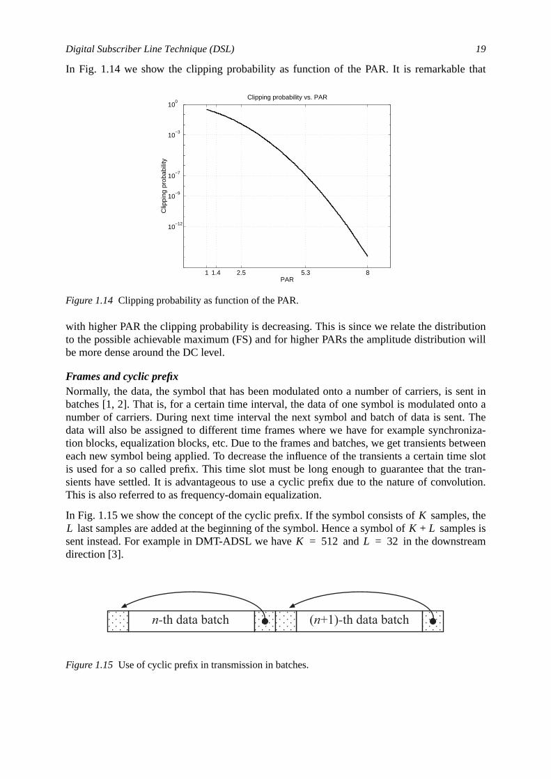
Digital Subscriber Line Technique (DSL) 19
that
tionwill
ent innto a. Theniza-tweene slottran-
lution.
, theples isam
In Fig. 1.14 we show the clipping probability as function of the PAR. It is remarkable
with higher PAR the clipping probability is decreasing. This is since we relate the distributo the possible achievable maximum (FS) and for higher PARs the amplitude distributionbe more dense around the DC level.
Frames and cyclic prefixNormally, the data, the symbol that has been modulated onto a number of carriers, is sbatches [1, 2]. That is, for a certain time interval, the data of one symbol is modulated onumber of carriers. During next time interval the next symbol and batch of data is sentdata will also be assigned to different time frames where we have for example synchrotion blocks, equalization blocks, etc. Due to the frames and batches, we get transients beeach new symbol being applied. To decrease the influence of the transients a certain timis used for a so called prefix. This time slot must be long enough to guarantee that thesients have settled. It is advantageous to use a cyclic prefix due to the nature of convoThis is also referred to as frequency-domain equalization.
In Fig. 1.15 we show the concept of the cyclic prefix. If the symbol consists of sampleslast samples are added at the beginning of the symbol. Hence a symbol of sam
sent instead. For example in DMT-ADSL we have and in the downstredirection [3].
Figure 1.14 Clipping probability as function of the PAR.
Figure 1.15 Use of cyclic prefix in transmission in batches.
1 1.4 2.5 5.3 8
10−12
10−9
10−7
10−3
100
Clipping probability vs. PAR
Clip
ping
pro
babi
lity
PAR
KL K L+
K 512= L 32=
n-th data batch (n+1)-th data batch
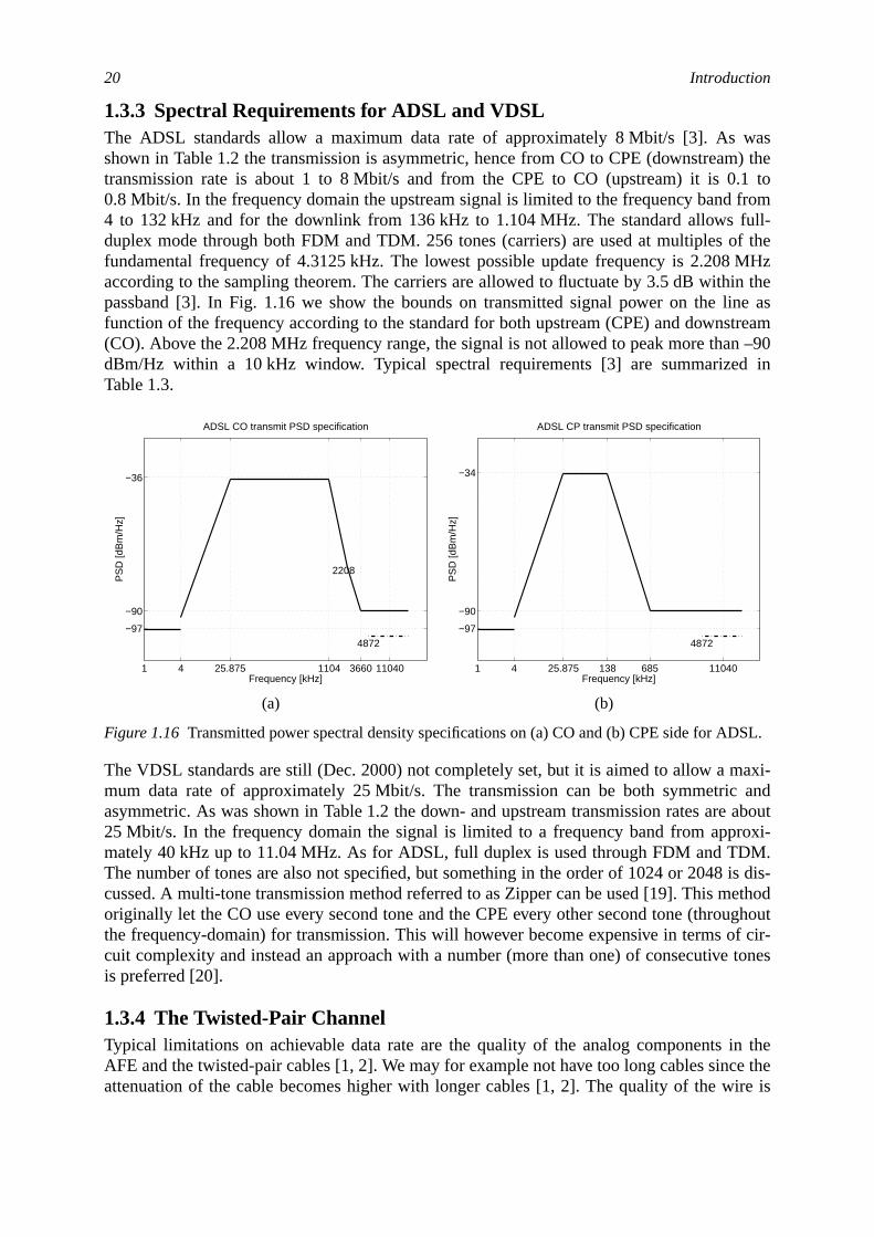
20 Introduction
was) the
.1 tofromull-f theMHzn thene astreamn –90
in
axi-andabout
roxi-M.is dis-ethodghoutf cir-tones
n thee the
ire is
SL.
1.3.3 Spectral Requirements for ADSL and VDSLThe ADSL standards allow a maximum data rate of approximately 8 Mbit/s [3]. Asshown in Table 1.2 the transmission is asymmetric, hence from CO to CPE (downstreamtransmission rate is about 1 to 8 Mbit/s and from the CPE to CO (upstream) it is 00.8 Mbit/s. In the frequency domain the upstream signal is limited to the frequency band4 to 132 kHz and for the downlink from 136 kHz to 1.104 MHz. The standard allows fduplex mode through both FDM and TDM. 256 tones (carriers) are used at multiples ofundamental frequency of 4.3125 kHz. The lowest possible update frequency is 2.208according to the sampling theorem. The carriers are allowed to fluctuate by 3.5 dB withipassband [3]. In Fig. 1.16 we show the bounds on transmitted signal power on the lifunction of the frequency according to the standard for both upstream (CPE) and downs(CO). Above the 2.208 MHz frequency range, the signal is not allowed to peak more thadBm/Hz within a 10 kHz window. Typical spectral requirements [3] are summarizedTable 1.3.
The VDSL standards are still (Dec. 2000) not completely set, but it is aimed to allow a mmum data rate of approximately 25 Mbit/s. The transmission can be both symmetricasymmetric. As was shown in Table 1.2 the down- and upstream transmission rates are25 Mbit/s. In the frequency domain the signal is limited to a frequency band from appmately 40 kHz up to 11.04 MHz. As for ADSL, full duplex is used through FDM and TDThe number of tones are also not specified, but something in the order of 1024 or 2048cussed. A multi-tone transmission method referred to as Zipper can be used [19]. This moriginally let the CO use every second tone and the CPE every other second tone (throuthe frequency-domain) for transmission. This will however become expensive in terms ocuit complexity and instead an approach with a number (more than one) of consecutiveis preferred [20].
1.3.4 The Twisted-Pair ChannelTypical limitations on achievable data rate are the quality of the analog components iAFE and the twisted-pair cables [1, 2]. We may for example not have too long cables sincattenuation of the cable becomes higher with longer cables [1, 2]. The quality of the w
(a) (b)
Figure 1.16 Transmitted power spectral density specifications on (a) CO and (b) CPE side for AD
1 4 25.875 1104 3660 11040
−97
−90
−36
2208
4872
ADSL CO transmit PSD specification
PS
D [d
Bm
/Hz]
Frequency [kHz]1 4 25.875 138 685 11040
−97
−90
−34
4872
ADSL CP transmit PSD specification
PS
D [d
Bm
/Hz]
Frequency [kHz]
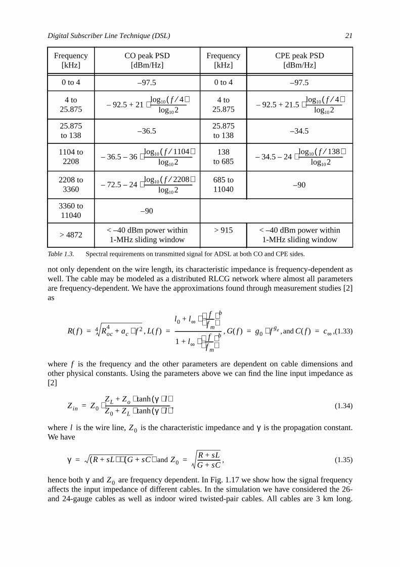
Digital Subscriber Line Technique (DSL) 21
ent aseters
dies [2]
ns andnce as
stant.
uencye 26-long.
not only dependent on the wire length, its characteristic impedance is frequency-dependwell. The cable may be modeled as a distributed RLCG network where almost all paramare frequency-dependent. We have the approximations found through measurement stuas
, , ,and ,(1.33)
where is the frequency and the other parameters are dependent on cable dimensioother physical constants. Using the parameters above we can find the line input impeda[2]
, (1.34)
where is the wire line, is the characteristic impedance and is the propagation conWe have
and , (1.35)
hence both and are frequency dependent. In Fig. 1.17 we show how the signal freqaffects the input impedance of different cables. In the simulation we have considered thand 24-gauge cables as well as indoor wired twisted-pair cables. All cables are 3 km
Frequency[kHz]
CO peak PSD[dBm/Hz]
Frequency[kHz]
CPE peak PSD[dBm/Hz]
0 to 4 0 to 4
4 to25.875
4 to25.875
25.875to 138
25.875to 138
1104 to2208
138to 685
2208 to3360
685 to11040
3360 to11040
> 4872< –40 dBm power within1-MHz sliding window
> 915 < –40 dBm power within1-MHz sliding window
Table 1.3. Spectral requirements on transmitted signal for ADSL at both CO and CPE sides.
97.5– 97.5–
92.5– 21f 4⁄( )log10
2log10
---------------------------⋅+ 92.5– 21.5f 4⁄( )log10
2log10
---------------------------⋅+
36.5– 34.5–
36.5– 36f 1104⁄( )log10
2log10
------------------------------------⋅– 34.5– 24f 138⁄( )log10
2log10
---------------------------------⋅–
72.5– 24f 2208⁄( )log10
2log10
------------------------------------⋅– 90–
90–
R f( ) Roc4
ac f 2⋅+4= L f( )
l0 l∞f
f m------
b⋅+
1 l∞f
f m------
b⋅+
-----------------------------------= G f( ) g0 f ge⋅= C f( ) c∞=
f
Zin Z0
ZL Zo γ l⋅( )tanh⋅+
Z0 ZL γ l⋅( )tanh⋅+------------------------------------------------⋅=
l Z0 γ
γ R sL+( ) G sC+( )⋅= Z0R sL+G sC+-----------------=
γ Z0
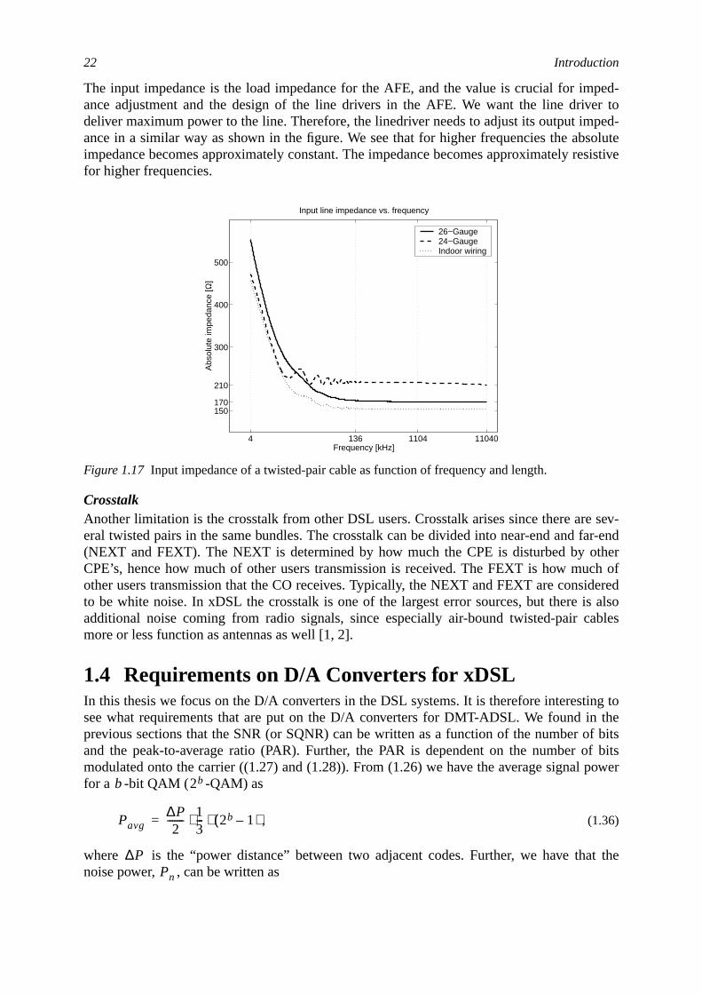
22 Introduction
ped-er toped-soluteesistive
e sev-ar-endtherch ofdereds alsoables
ng tothe
f bitsf bits
power
at the
The input impedance is the load impedance for the AFE, and the value is crucial for imance adjustment and the design of the line drivers in the AFE. We want the line drivdeliver maximum power to the line. Therefore, the linedriver needs to adjust its output imance in a similar way as shown in the figure. We see that for higher frequencies the abimpedance becomes approximately constant. The impedance becomes approximately rfor higher frequencies.
CrosstalkAnother limitation is the crosstalk from other DSL users. Crosstalk arises since there areral twisted pairs in the same bundles. The crosstalk can be divided into near-end and f(NEXT and FEXT). The NEXT is determined by how much the CPE is disturbed by oCPE’s, hence how much of other users transmission is received. The FEXT is how muother users transmission that the CO receives. Typically, the NEXT and FEXT are consito be white noise. In xDSL the crosstalk is one of the largest error sources, but there iadditional noise coming from radio signals, since especially air-bound twisted-pair cmore or less function as antennas as well [1, 2].
1.4 Requirements on D/A Converters for xDSLIn this thesis we focus on the D/A converters in the DSL systems. It is therefore interestisee what requirements that are put on the D/A converters for DMT-ADSL. We found inprevious sections that the SNR (or SQNR) can be written as a function of the number oand the peak-to-average ratio (PAR). Further, the PAR is dependent on the number omodulated onto the carrier ((1.27) and (1.28)). From (1.26) we have the average signalfor a -bit QAM ( -QAM) as
, (1.36)
where is the “power distance” between two adjacent codes. Further, we have thnoise power, , can be written as
Figure 1.17 Input impedance of a twisted-pair cable as function of frequency and length.
4 136 1104 11040
150170
210
300
400
500
Input line impedance vs. frequencyA
bsol
ute
impe
danc
e [Ω
]
Frequency [kHz]
26−Gauge 24−Gauge Indoor wiring
b 2b
Pavg∆P2
------- 13--- 2b 1–( )⋅ ⋅=
∆PPn
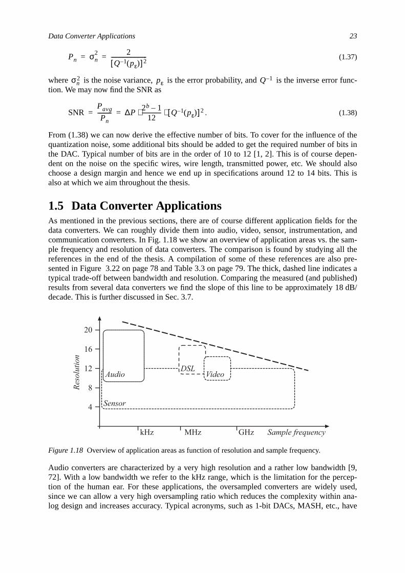
Data Converter Applications 23
unc-
f thebits inen-alsohis is
r the, andsam-ll theo pre-ates a
ished)8 dB/
th [9,ep-used,
ana-, have
(1.37)
where is the noise variance, is the error probability, and is the inverse error ftion. We may now find the SNR as
. (1.38)
From (1.38) we can now derive the effective number of bits. To cover for the influence oquantization noise, some additional bits should be added to get the required number ofthe DAC. Typical number of bits are in the order of 10 to 12 [1, 2]. This is of course depdent on the noise on the specific wires, wire length, transmitted power, etc. We shouldchoose a design margin and hence we end up in specifications around 12 to 14 bits. Talso at which we aim throughout the thesis.
1.5 Data Converter ApplicationsAs mentioned in the previous sections, there are of course different application fields fodata converters. We can roughly divide them into audio, video, sensor, instrumentationcommunication converters. In Fig. 1.18 we show an overview of application areas vs. theple frequency and resolution of data converters. The comparison is found by studying areferences in the end of the thesis. A compilation of some of these references are alssented in Figure 3.22 on page 78 and Table 3.3 on page 79. The thick, dashed line indictypical trade-off between bandwidth and resolution. Comparing the measured (and publresults from several data converters we find the slope of this line to be approximately 1decade. This is further discussed in Sec. 3.7.
Audio converters are characterized by a very high resolution and a rather low bandwid72]. With a low bandwidth we refer to the kHz range, which is the limitation for the perction of the human ear. For these applications, the oversampled converters are widelysince we can allow a very high oversampling ratio which reduces the complexity withinlog design and increases accuracy. Typical acronyms, such as 1-bit DACs, MASH, etc.
Figure 1.18 Overview of application areas as function of resolution and sample frequency.
Pn σn2 2
Q 1– pε( )[ ]2--------------------------= =
σn2 pε Q 1–
SNRPavg
Pn---------- ∆P
2b 1–12
-------------- Q 1– pε( )[ ]2⋅ ⋅= =
Sample frequency
Res
olut
ion
kHz MHz GHz
20
16
12
8
4 Sensor
DSLVideoAudio

24 Introduction
alsonvert-
nt towill
dulate
ration.vide a
uencyays as
become a kind of commercial tag displayed on several CD players.
The video converters require a higher bandwidth [53, 54, 56, 63]. Video converters havebeen applicable in the telecommunications applications, but nowadays we must have coers with even higher performance for communications. In communications, we wareplace the analog circuits with as digital circuits as much possible. This implies that wepush the interface closer and closer to the channel. For radio applications we want to mothe signal in the digital domain as is done for the DSL applications.
Instrumentation converters are used in measurement equipment and for signal geneThese converters are typically implemented in special, expensive technologies to provery high linearity [114].
Sensor converters are very application specific and the common resolution and freqbandwidth vary between the extremes. We have for example image sensors in pixel arrwell as D/A converters controlling computer drives, etc.
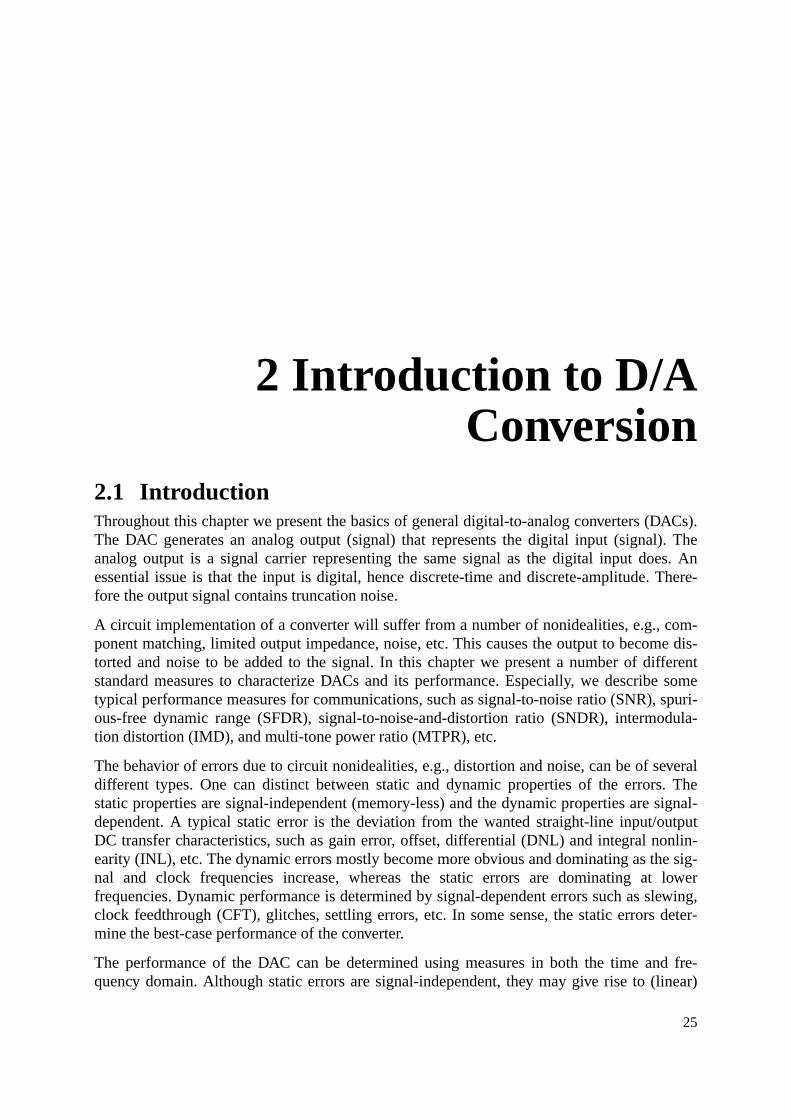
ACs).. Thes. Anhere-
m-e dis-
ferentsome
spuri-dula-
veral. Thesignal-tputnlin-e sig-lower
lewing,deter-
d fre-near)
2 Introduction to D/AConversion
2.1 IntroductionThroughout this chapter we present the basics of general digital-to-analog converters (DThe DAC generates an analog output (signal) that represents the digital input (signal)analog output is a signal carrier representing the same signal as the digital input doeessential issue is that the input is digital, hence discrete-time and discrete-amplitude. Tfore the output signal contains truncation noise.
A circuit implementation of a converter will suffer from a number of nonidealities, e.g., coponent matching, limited output impedance, noise, etc. This causes the output to becomtorted and noise to be added to the signal. In this chapter we present a number of difstandard measures to characterize DACs and its performance. Especially, we describetypical performance measures for communications, such as signal-to-noise ratio (SNR),ous-free dynamic range (SFDR), signal-to-noise-and-distortion ratio (SNDR), intermotion distortion (IMD), and multi-tone power ratio (MTPR), etc.
The behavior of errors due to circuit nonidealities, e.g., distortion and noise, can be of sedifferent types. One can distinct between static and dynamic properties of the errorsstatic properties are signal-independent (memory-less) and the dynamic properties aredependent. A typical static error is the deviation from the wanted straight-line input/ouDC transfer characteristics, such as gain error, offset, differential (DNL) and integral noearity (INL), etc. The dynamic errors mostly become more obvious and dominating as thnal and clock frequencies increase, whereas the static errors are dominating atfrequencies. Dynamic performance is determined by signal-dependent errors such as sclock feedthrough (CFT), glitches, settling errors, etc. In some sense, the static errorsmine the best-case performance of the converter.
The performance of the DAC can be determined using measures in both the time anquency domain. Although static errors are signal-independent, they may give rise to (li
25
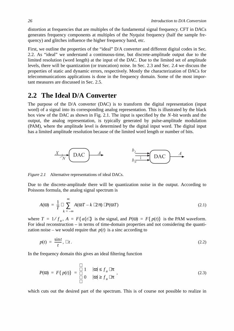
26 Introduction to D/A Conversion
ACsle fre-
ec.o thede
ss thes forpor-
putblackthe
lationput
g to
.anti-
ize in
distortion at frequencies that are multiples of the fundamental signal frequency. CFT in Dgenerates frequency components at multiples of the Nyquist frequency (half the sampquency) and glitches influence the higher frequency band, etc.
First, we outline the properties of the “ideal” D/A converter and different digital codes in S2.2. As “ideal” we understand a continuous-time, but discrete-amplitude output due tlimited resolution (word length) at the input of the DAC. Due to the limited set of amplitulevels, there will be quantization (or truncation) noise. In Sec. 2.3 and Sec. 2.4 we discuproperties of static and dynamic errors, respectively. Mostly the characterization of DACtelecommunications applications is done in the frequency domain. Some of the most imtant measures are discussed in Sec. 2.5.
2.2 The Ideal D/A ConverterThe purpose of the D/A converter (DAC) is to transform the digital representation (inword) of a signal into its corresponding analog representation. This is illustrated by thebox view of the DAC as shown in Fig. 2.1. The input is specified by the -bit words andoutput, the analog representation, is typically generated by pulse-amplitude modu(PAM), where the amplitude level is determined by the digital input word. The digital inhas a limited amplitude resolution because of the limited word length or number of bits.
Due to the discrete-amplitude there will be quantization noise in the output. AccordinPoissons formula, the analog signal spectrum is
(2.1)
where , is the signal, and is the PAM waveformFor ideal reconstruction – in terms of time-domain properties and not considering the quzation noise – we would require that is a sinc according to
, . (2.2)
In the frequency domain this gives an ideal filtering function
, (2.3)
which cuts out the desired part of the spectrum. This is of course not possible to real
Figure 2.1 Alternative representations of ideal DACs.
N
DACN
X ADAC A
b1
bN
A ω( )1T--- A ωT k 2π⋅–( ) P ωT( )⋅
k ∞–=
∞
∑⋅=
T 1 f u⁄= A F a t( ) = P ω( ) F p t( ) =
p t( )
p t( ) tsint
---------= t∀
P ω( ) F p t( ) 1 ω f u π⋅≤
0 ω f u π⋅≥
= =
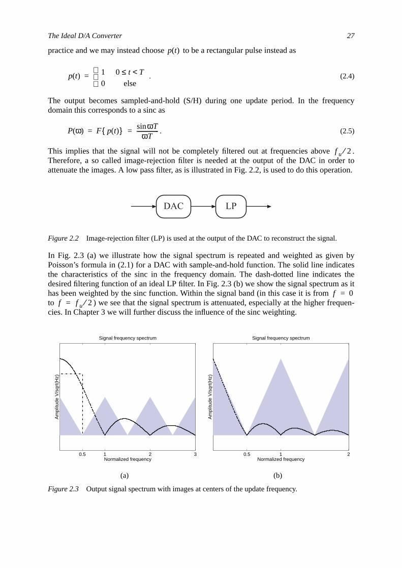
The Ideal D/A Converter 27
uency
.er toration.
n bytess the
as it
quen-
practice and we may instead choose to be a rectangular pulse instead as
. (2.4)
The output becomes sampled-and-hold (S/H) during one update period. In the freqdomain this corresponds to a sinc as
. (2.5)
This implies that the signal will not be completely filtered out at frequencies aboveTherefore, a so called image-rejection filter is needed at the output of the DAC in ordattenuate the images. A low pass filter, as is illustrated in Fig. 2.2, is used to do this ope
In Fig. 2.3 (a) we illustrate how the signal spectrum is repeated and weighted as givePoisson’s formula in (2.1) for a DAC with sample-and-hold function. The solid line indicathe characteristics of the sinc in the frequency domain. The dash-dotted line indicatedesired filtering function of an ideal LP filter. In Fig. 2.3 (b) we show the signal spectrumhas been weighted by the sinc function. Within the signal band (in this case it is fromto ) we see that the signal spectrum is attenuated, especially at the higher frecies. In Chapter 3 we will further discuss the influence of the sinc weighting.
Figure 2.2 Image-rejection filter (LP) is used at the output of the DAC to reconstruct the signal.
(a) (b)
Figure 2.3 Output signal spectrum with images at centers of the update frequency.
p t( )
p t( ) 1 0 t T<≤0 else
=
P ω( ) F p t( ) ωTsinωT
----------------= =
f u 2⁄
DAC LP
f 0=f f u 2⁄=
0.5 1 2 3
Signal frequency spectrum
Am
plitu
de V
/sqr
t(H
z)
Normalized frequency0.5 1 2
Signal frequency spectrum
Am
plitu
de V
/sqr
t(H
z)
Normalized frequency
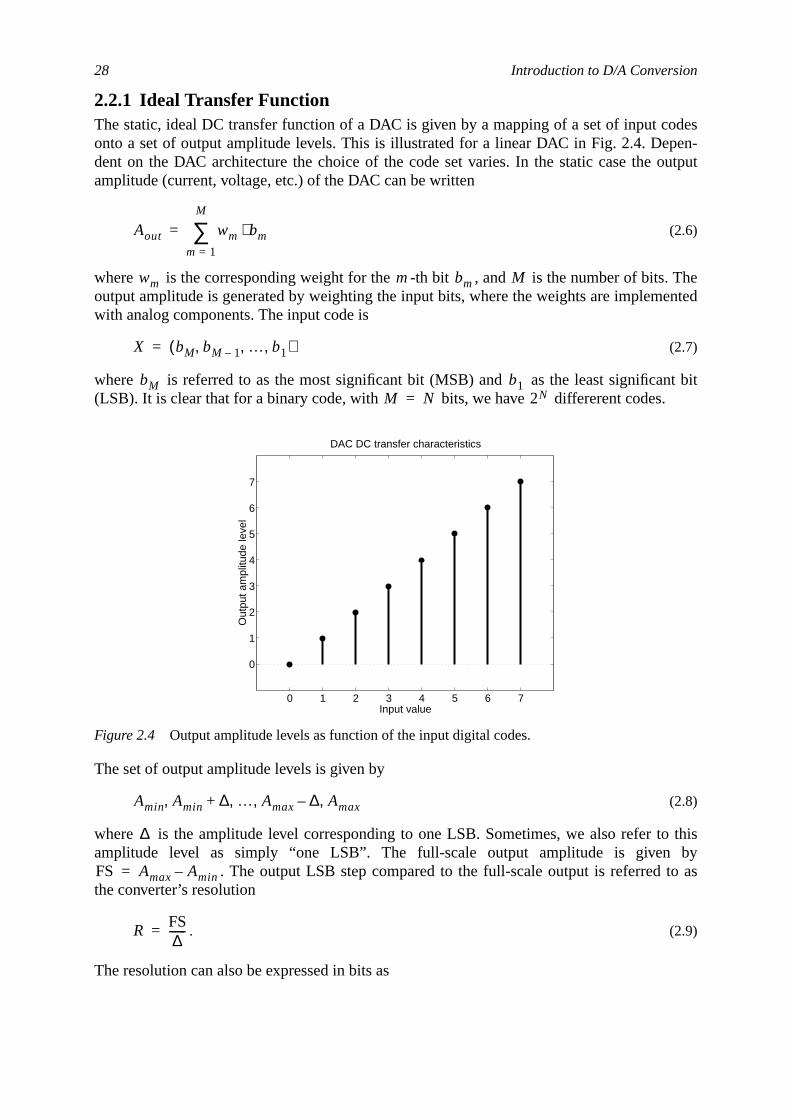
28 Introduction to D/A Conversion
desen-
output
Theented
t bit
o thisbyas
2.2.1 Ideal Transfer FunctionThe static, ideal DC transfer function of a DAC is given by a mapping of a set of input coonto a set of output amplitude levels. This is illustrated for a linear DAC in Fig. 2.4. Depdent on the DAC architecture the choice of the code set varies. In the static case theamplitude (current, voltage, etc.) of the DAC can be written
(2.6)
where is the corresponding weight for the -th bit , and is the number of bits.output amplitude is generated by weighting the input bits, where the weights are implemwith analog components. The input code is
(2.7)
where is referred to as the most significant bit (MSB) and as the least significan(LSB). It is clear that for a binary code, with bits, we have differerent codes.
The set of output amplitude levels is given by
(2.8)
where is the amplitude level corresponding to one LSB. Sometimes, we also refer tamplitude level as simply “one LSB”. The full-scale output amplitude is given
. The output LSB step compared to the full-scale output is referred tothe converter’s resolution
. (2.9)
The resolution can also be expressed in bits as
Figure 2.4 Output amplitude levels as function of the input digital codes.
Aout wm bm⋅m 1=
M
∑=
wm m bm M
X bM bM 1– … b1, , ,( )=
bM b1M N= 2N
0 1 2 3 4 5 6 7
0
1
2
3
4
5
6
7
DAC DC transfer characteristics
Out
put a
mpl
itude
leve
l
Input value
Amin Amin ∆+ … Amax ∆– Amax, , , ,
∆
FS Amax Amin–=
RFS∆------=
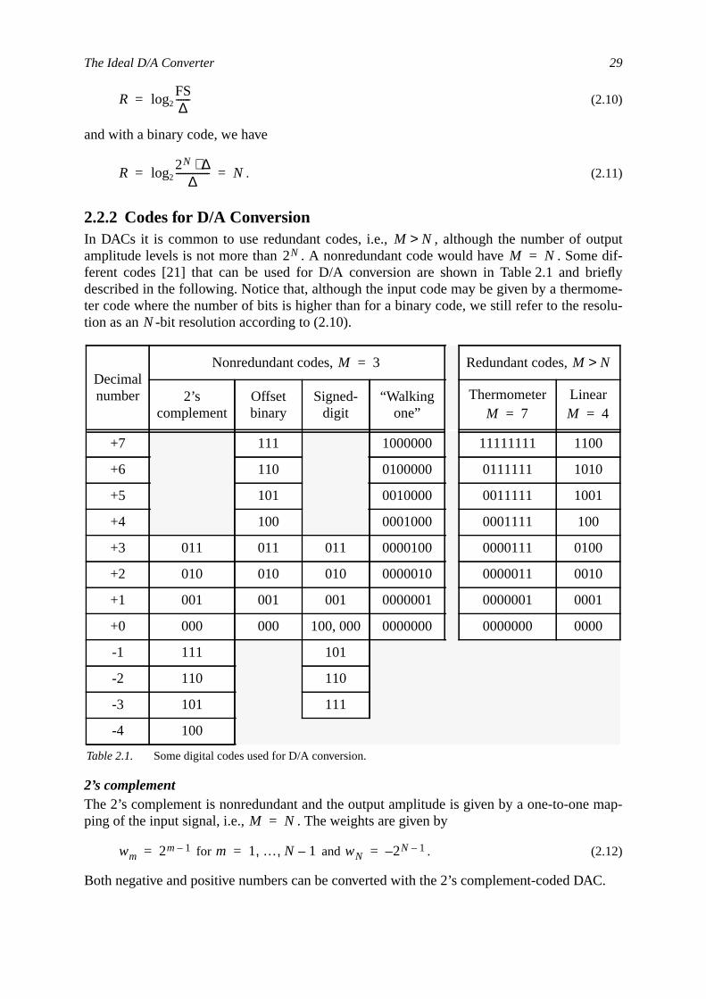
The Ideal D/A Converter 29
tputdif-
rieflyome-solu-
map-
AC.
(2.10)
and with a binary code, we have
. (2.11)
2.2.2 Codes for D/A ConversionIn DACs it is common to use redundant codes, i.e., , although the number of ouamplitude levels is not more than . A nonredundant code would have . Someferent codes [21] that can be used for D/A conversion are shown in Table 2.1 and bdescribed in the following. Notice that, although the input code may be given by a thermter code where the number of bits is higher than for a binary code, we still refer to the retion as an -bit resolution according to (2.10).
2’s complementThe 2’s complement is nonredundant and the output amplitude is given by a one-to-oneping of the input signal, i.e., . The weights are given by
for and . (2.12)
Both negative and positive numbers can be converted with the 2’s complement-coded D
Decimalnumber
Nonredundant codes, Redundant codes,
2’scomplement
Offsetbinary
Signed-digit
“Walkingone”
Thermometer Linear
+7 111 1000000 11111111 1100
+6 110 0100000 0111111 1010
+5 101 0010000 0011111 1001
+4 100 0001000 0001111 100
+3 011 011 011 0000100 0000111 0100
+2 010 010 010 0000010 0000011 0010
+1 001 001 001 0000001 0000001 0001
+0 000 000 100, 000 0000000 0000000 0000
-1 111 101
-2 110 110
-3 101 111
-4 100
Table 2.1. Some digital codes used for D/A conversion.
RFS∆------log2=
R2N ∆⋅
∆--------------log2 N= =
M N>2N M N=
N
M 3= M N>
M 7= M 4=
M N=
wm 2m 1–= m 1 … N 1–, ,= wN 2N 1––=

30 Introduction to D/A Conversion
ing of
ier toidelystly
n by a00 or
y one
theD/A
rate the
ng the00100,
1. In
l valueld bealso
Offset binaryThe binary offset is nonredundant as well and the output is given by a one-to-one mappthe input, i.e., . The weights are given by
for . (2.13)
Only positive numbers can be realized with the offset binary coded DAC. Since it is easimplement positive weights only due to matching reasons, the binary offset code is wused, and throughout the thesis, when illustrating the operation of the DAC, we will mouse the binary offset code.
Signed-digitThe signed-digit code is nonredundant and the output, except for the zero value, is giveone-to-one mapping of the input value. The zero can be represented by either 100...0000...000. We have where the weights are given by
for . (2.14)
Both negative and positive numbers are represented with the signed-digit code.
“Walking one”The “walking one” code is nonredundant, i.e., every word corresponds to one and onloutput analog value. The weights are given by
for , (2.15)
where is the number of bits and weights. The walking-one code is similar tothermometer code and is mostly used for weight selection in for example a resistor-stringconverter (see Sec. 3.5.3).
Thermometer codeThe thermometer code is redundant and hence several different input codes can genesame output signal. All weights are equally large and given by
for . (2.16)
This implies that in a thermometer code the number of bits is given by
. (2.17)
For higher resolutions we have that and hence there are many codes generatisame output. For example, the codes 1000000, 0100000, 0010000, 0001000, 000000010, and 0000001, all give the same output corresponding to the decimal value;fact, there are
, (2.18)
different codes corresponding to the same analog output corresponding to the decima. This redundant property is very advantegous in some implementations, and it shou
used in order to manipulate the digital input to gain a higher DAC performance. This is
M N=
wm 2m 1–= m 1 … N, ,=
M N=
wm 1–( )wN 2m 1–⋅= m 1 … N 1–, ,=
wm 2m 1–= m 1 … M, ,=
M 2N 1–=
wm 1= m 1 … M, ,=
M 2N 1–=
2N N»
Mm
2N 1–m
= m 0 … 2N 1–, ,=
m
Static Performance 31
equaltching.
of
t cor-es of
ar code
qualitysig-
easure-
as thelin-
ng ash, we
discussed in Chapter 7.
The thermometer code is widely used in D/A converters since a number of weights areand hence they can be laid out with special techniques to achieve a good device maWith a thermometer coded input, unwanted glitches can be minimized.
Linear codeThe linear code is also redundant, but the weights are given by
, for . (2.19)
The required number of bits (and weights), , is found by comparing the total sumweights as
, (2.20)
giving
. (2.21)
To find the best integer value on we have the upper bound as
. (2.22)
For high resolutions, i.e., is large, we have that
. (2.23)
The code is redundant and, for example, the codes and give the same outpuresponding to the decimal value 4. The linear code is a code in-between the two extremthe binary and thermometer code. The advantages and disadvantages of using the linein D/A conversion is discussed in Chapter 7.
2.3 Static PerformanceDependent on application, different performance measures are used to characterize theand performance of a D/A converter. In many telecommunication applications, multi-tonenalling is used and in those cases (or in general), static measures or even single-tone mments will not give all the necessary information to fully characterize the DAC.
In this section we outline some of the most common static performance measures, suchquantization noise, gain and offset error, differential nonlinearity (DNL), and integral nonearity (INL).
2.3.1 Quantization or Truncation NoiseDependent on one’s view, the DAC does not perform any quantization or truncation as lothe resolution of the converter is as high (or higher) as the input word length. Eventhoug
wm m= m 1 … M, ,=
M
mm 1=
M
∑ 2m 1–
m 1=
N
∑ 2N 1–= =
M M 1+( )⋅2
----------------------------- 2N 1–=
M
M 1 8 2N 1–( )⋅+ 1–2
--------------------------------------------------=
N
M 2N 1+
2-------------
≈
1000 0101
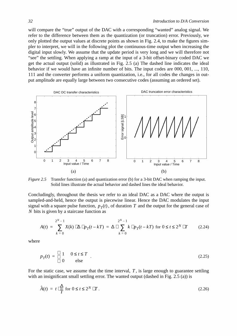
32 Introduction to D/A Conversion
Wely, we
sim-thenotweideal110,
n out-et).
ut isinput
se of
ettling
ut.
will compare the “true” output of the DAC with a corresponding “wanted” analog signal.refer to the difference between them as the quantization (or truncation) error. Previousonly plotted the output values at discrete points as shown in Fig. 2.4, to make the figurespler to interpret, we will in the following plot the continuous-time output when increasingdigital input slowly. We assume that the update period is very long and we will therefore“see” the settling. When applying a ramp at the input of a 3-bit offset-binary coded DACget the actual output (solid) as illustrated in Fig. 2.5 (a) The dashed line indicates thebehavior if we would have an infinite number of bits. The input codes are 000, 001, ...,111 and the converter performs a uniform quantization, i.e., for all codes the changes iput amplitude are equally large between two consecutive codes (assuming an ordered s
Concludingly, throughout the thesis we refer to an ideal DAC as a DAC where the outpsampled-and-held, hence the output is piecewise linear. Hence the DAC modulates thesignal with a square pulse function, , of duration and the output for the general ca
bits is given by a staircase function as
for (2.24)
where
. (2.25)
For the static case, we assume that the time interval, , is large enough to guarantee swith an insignificant small settling error. The wanted output (dashed in Fig. 2.5 (a)) is
for . (2.26)
(a) (b)
Figure 2.5 Transfer function (a) and quantization error (b) for a 3-bit DAC when ramping the inpSolid lines illustrate the actual behavior and dashed lines the ideal behavior.
0 1 2 3 4 5 6 7 8
0
1
2
3
4
5
6
7
8
DAC DC transfer characteristics
Out
put a
mpl
itude
leve
l
Input value / Time0 1 2 3 4 5 6 7 8
0
1
DAC truncation error characteristics
Err
or s
igna
l [LS
B]
Input value / Time
pT t( ) TN
A t( ) X k( ) ∆ pT t kT–( )⋅ ⋅k 0=
2N 1–
∑ ∆ k pT t kT–( )⋅k 0=
2N 1–
∑⋅= = 0 t 2N T⋅≤ ≤
pT t( ) 1 0 t T≤ ≤0 else
=
T
A t( ) t∆T---⋅= 0 t 2N T⋅≤ ≤
Static Performance 33
evelset,hole
r canents
e, thehave
restingum
tely
.28)
ouldtherto the.
We have the difference signal, the quantization error, as
. (2.27)
This is illustrated in Fig. 2.5 (b). We see that with this definition (2.27), there is an offset lof , but this will not be considered as a quantization error. Neglecting this offwe can find the RMS value of the error. It is obvious that the RMS value of over the wramp is the same as during one time period . We have
(2.28)
and
. (2.29)
If the resolution of the data converter is reasonably high (higher than 4 or 5 bits) the errobe regarded as white noise [9], otherwise if the number of bits is low, distortion componare also found in the output spectrum. If the conversion error is treated as white noispower spectral density (PSD) will be uniformly distributed over the frequency range. Wethat
, (2.30)
where is the update frequency of the DAC.
Sinusoidal signals are often used to characterize a data converter and it is therefore inteto calulate the ideal signal-to-noise ratio (SNR) with such an input signal. The maxim(AC) amplitude without causing saturation of a sinusoidal input signal is approxima
and the average power of the sine wave becomes
. (2.31)
The SNR of an ideal converter with a sinusoidal input signal is found by combining (2and (2.31)
, (2.32)
which is more conveniently expressed in decibel by the well-known formula
dB. (2.33)
The SNR is increased by approximately 6 dB for each additional bit in the converter. It shbe noted that (2.33) holds if the input is a full-scale sine wave. The effect of having otypes of input signals is discussed in Sec. 2.5.10. Sometimes the SNR with respectquantization noise is referred to as signal-to-quantization noise ratio and denoted SQNR
ε t( ) A t( ) A t( )–=
εos ∆ 2⁄=ε
T
Pq εRMS2 1
T--- ε2 t( ) td
0
T
∫ εos2–
1T--- t
T--- ∆⋅
2td
0
T
∫ ∆2---
2– ∆2
12------= = = =
εRMS Pq∆
2 3----------= =
Sq f( )Pq
f u 2⁄------------
εRMS2
f u 2⁄------------ ∆2
6 f u⋅-------------= = =
f u
∆ 2N 1–⋅
Ps∆ 2N 1–⋅( )2
2-----------------------------=
SNRPs
Pq------ ∆ 2N 1–⋅( )2 2⁄
∆2 12⁄------------------------------------
32--- 2⋅
2N= = =
SNR 10 Ps Pq⁄( )log10⋅ 6.02 N 1.76+⋅≈=
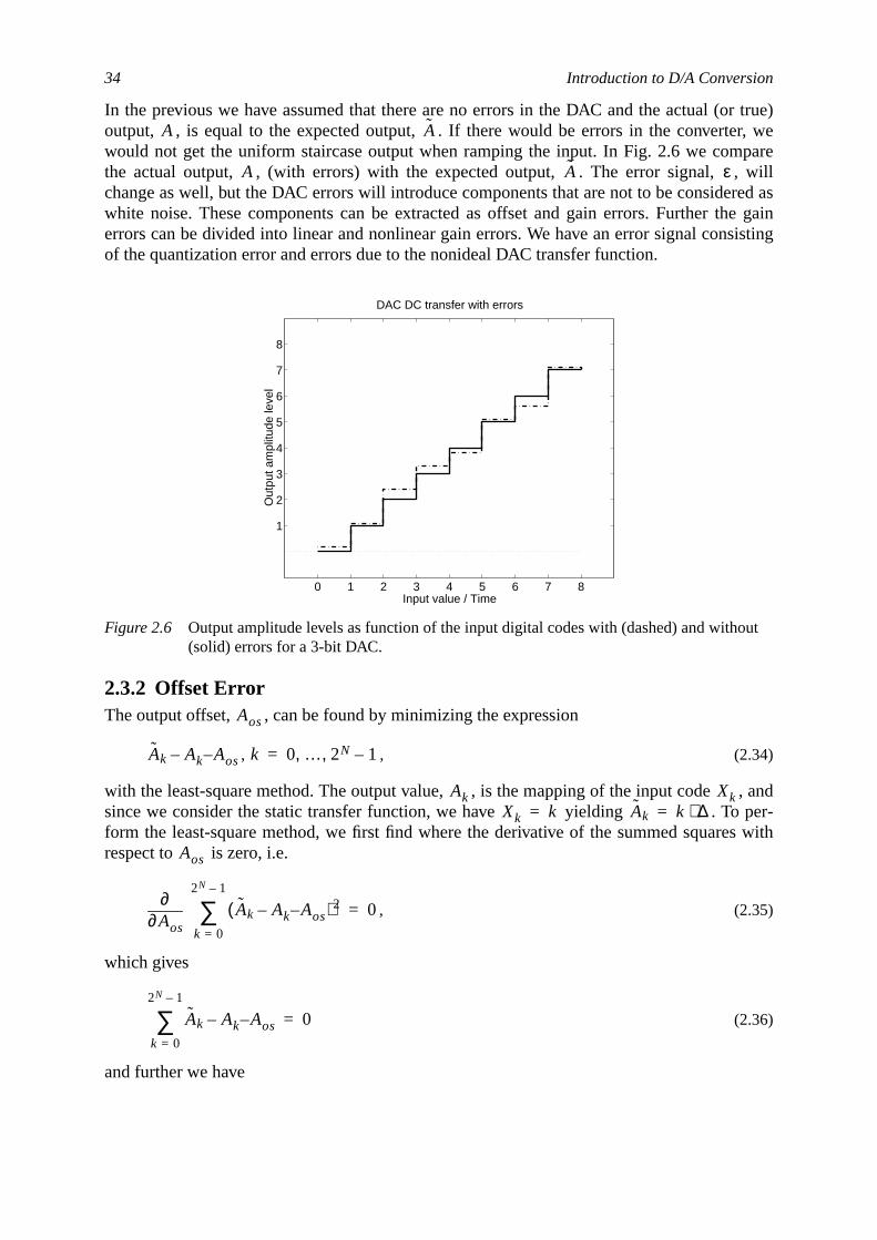
34 Introduction to D/A Conversion
r true)r, weparewillred ase gainisting
, ander-
s with
out
In the previous we have assumed that there are no errors in the DAC and the actual (ooutput, , is equal to the expected output, . If there would be errors in the convertewould not get the uniform staircase output when ramping the input. In Fig. 2.6 we comthe actual output, , (with errors) with the expected output, . The error signal, ,change as well, but the DAC errors will introduce components that are not to be considewhite noise. These components can be extracted as offset and gain errors. Further therrors can be divided into linear and nonlinear gain errors. We have an error signal consof the quantization error and errors due to the nonideal DAC transfer function.
2.3.2 Offset ErrorThe output offset, , can be found by minimizing the expression
, , (2.34)
with the least-square method. The output value, , is the mapping of the input codesince we consider the static transfer function, we have yielding . To pform the least-square method, we first find where the derivative of the summed squarerespect to is zero, i.e.
, (2.35)
which gives
(2.36)
and further we have
Figure 2.6 Output amplitude levels as function of the input digital codes with (dashed) and with(solid) errors for a 3-bit DAC.
A A
A A ε
0 1 2 3 4 5 6 7 8
1
2
3
4
5
6
7
8
DAC DC transfer with errors
Out
put a
mpl
itude
leve
l
Input value / Time
Aos
Ak Ak– Aos– k 0 … 2N 1–, ,=
Ak XkXk k= Ak k ∆⋅=
Aos
Aos∂∂
Ak Ak– Aos–( )2
k 0=
2N 1–
∑ 0=
Ak Ak– Aos–k 0=
2N 1–
∑ 0=
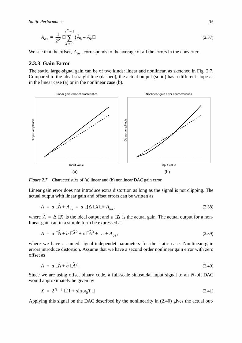
Static Performance 35
.
. 2.7.pe as
. The
non-
ar gainh zero
DAC
out-
. (2.37)
We see that the offset, , corresponds to the average of all the errors in the converter
2.3.3 Gain ErrorThe static, large-signal gain can be of two kinds: linear and nonlinear, as sketched in FigCompared to the ideal straight line (dashed), the actual output (solid) has a different sloin the linear case (a) or in the nonlinear case (b).
Linear gain error does not introduce extra distortion as long as the signal is not clippingactual output with linear gain and offset errors can be written as
, (2.38)
where is the ideal output and is the actual gain. The actual output for alinear gain can in a simple form be expressed as
, (2.39)
where we have assumed signal-independet parameters for the static case. Nonlineerrors introduce distortion. Assume that we have a second order nonlinear gain error witoffset as
. (2.40)
Since we are using offset binary code, a full-scale sinusoidal input signal to an -bitwould approximately be given by
. (2.41)
Applying this signal on the DAC described by the nonlinearity in (2.40) gives the actual
(a) (b)
Figure 2.7 Characteristics of (a) linear and (b) nonlinear DAC gain error.
Aos1
2N------ Ak Ak–( )
k 0=
2N 1–
∑⋅=
Aos
Linear gain error characteristics
Out
put a
mpl
itude
Input value
Nonlinear gain error characteristics
Out
put a
mpl
itude
Input value
A a A⋅ Aos+ a ∆ X⋅( )⋅ Aos+= =
A ∆ X⋅= a ∆⋅
A a A⋅ b A2⋅ c A3⋅ … Aos+ + + +=
A a A⋅ b A2⋅+=
N
X 2N 1– 1 ω0Tsin+( )⋅=
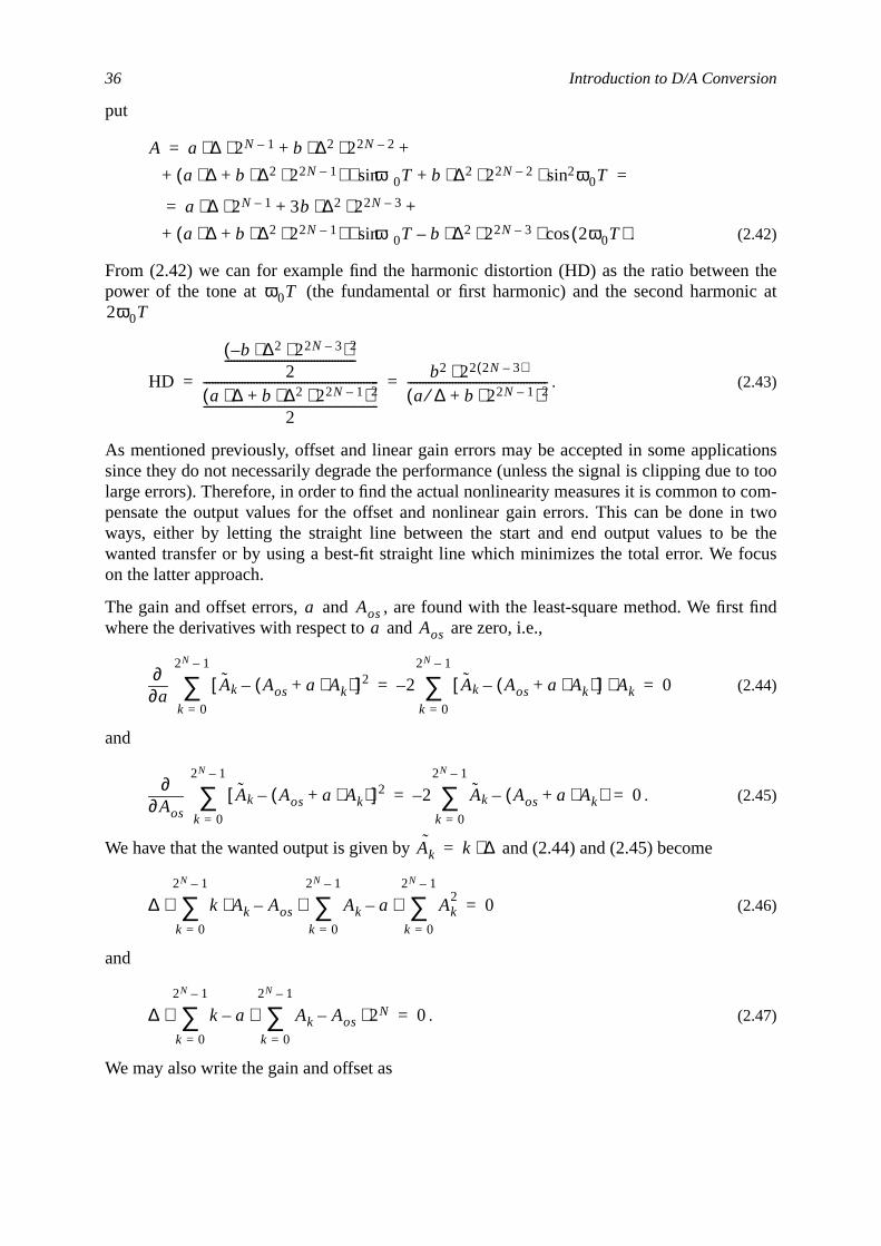
36 Introduction to D/A Conversion
theic at
ationsto too
com-in twoe theocus
t find
put
. (2.42)
From (2.42) we can for example find the harmonic distortion (HD) as the ratio betweenpower of the tone at (the fundamental or first harmonic) and the second harmon
. (2.43)
As mentioned previously, offset and linear gain errors may be accepted in some applicsince they do not necessarily degrade the performance (unless the signal is clipping duelarge errors). Therefore, in order to find the actual nonlinearity measures it is common topensate the output values for the offset and nonlinear gain errors. This can be doneways, either by letting the straight line between the start and end output values to bwanted transfer or by using a best-fit straight line which minimizes the total error. We fon the latter approach.
The gain and offset errors, and , are found with the least-square method. We firswhere the derivatives with respect to and are zero, i.e.,
(2.44)
and
. (2.45)
We have that the wanted output is given by and (2.44) and (2.45) become
(2.46)
and
. (2.47)
We may also write the gain and offset as
A a ∆ 2N 1–⋅ ⋅ b ∆2 22N 2–⋅⋅+ +=
a ∆⋅ b ∆2 22N 1–⋅⋅+( ) ω0Tsin⋅ b ∆2 22N 2–⋅ ω0Tsin2⋅ ⋅+ + =
a ∆ 2N 1–⋅ ⋅ 3b ∆2 22N 3–⋅⋅+ +=
a ∆⋅ b ∆2 22N 1–⋅⋅+( ) ω0Tsin⋅ b ∆2 22N 3– 2ω0T( )cos⋅ ⋅ ⋅–+
ω0T2ω0T
HD
b– ∆2 22N 3–⋅ ⋅( )2
2--------------------------------------------
a ∆⋅ b ∆2 22N 1–⋅⋅+( )2
2---------------------------------------------------------------------------------------------------------------------- b2 22 2N 3–( )⋅
a ∆⁄ b 22N 1–⋅+( )2-----------------------------------------------= =
a Aosa Aos
a∂∂
Ak Aos a Ak⋅+( )–[ ]2
k 0=
2N 1–
∑ 2– Ak Aos a Ak⋅+( )–[ ] Ak⋅k 0=
2N 1–
∑ 0= =
Aos∂∂
Ak Aos a Ak⋅+( )–[ ]2
k 0=
2N 1–
∑ 2– Ak Aos a Ak⋅+( )–k 0=
2N 1–
∑ 0= =
Ak˜ k ∆⋅=
∆ k Ak⋅k 0=
2N 1–
∑⋅ Aos Akk 0=
2N 1–
∑⋅– a Ak2
k 0=
2N 1–
∑⋅– 0=
∆ kk 0=
2N 1–
∑⋅ a Akk 0=
2N 1–
∑⋅– Aos 2N⋅– 0=
Static Performance 37
tegral
arityCn be2.5.viates
outputest-fit
d
(2.48)
and
, (2.49)
where the mean values are found over all , e.g.,
. (2.50)
These parameters should then be used for extracting for example the differential and innonlinearities as described in the next section.
2.3.4 Differential (DNL) and Integral Nonlinearity (INL)To find the nonlinear behavior of the DC transfer function we use the differential nonline(DNL) and the integral nonlinearity (INL) [7, 9]. In Fig. 2.8 (a) we show a part of the Dcharacteristics for the same DAC as in Fig. 2.6 and we illustrate how the DNL and INL cafound. The DNL and INL expresses the deviation from the straight line as shown in Fig.DNL expresses how much the difference in output level between two adjacent codes defrom the ideal LSB step
. (2.51)
Actually, the linear gain and offset are not of interest and therefore the measured/actualamplitude levels should be compensated for using the amplitude levels given by the bstraight line parameters from (2.48) and (2.49). The best-fit line is given by
(a) (b)
Figure 2.8 (a) Nonideal transfer characteristics illustrating INL and DNL errors in a 3-bit DAC an(b) compensated transfer characteristics.
aAk Ak⋅ Ak Ak⋅–
Ak2 Ak
2–----------------------------------------=
Aos Ak a Ak⋅–=
k
Ak1
2N------ Ak
k 0=
2N 1–
∑ ∆2N------ k
k 0=
2N 1–
∑ 2N 2N 1–( )⋅2 2N⋅
-------------------------------∆ 2N 1– ∆⋅≈= = =
∆
DNLk Ak Ak 1–– ∆–=
3 4 5
2
3
4
5
6
INL3
DNL5
∆
DAC DC transfer with errors
Out
put a
mpl
itude
leve
l
Input value / Time0 1 2 3 4 5 6 7 8
−0.5
0
0.5
DAC compensated DC transfer characteristics
Out
put a
mpl
itude
leve
l
Input value / Time
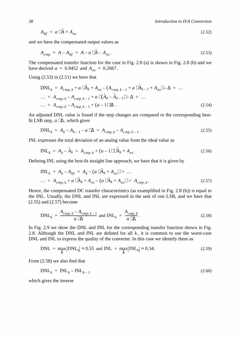
38 Introduction to D/A Conversion
d we
best-
ual tothat
Fig.ase
(2.52)
and we have the compensated output values as
. (2.53)
The compensated transfer function for the case in Fig. 2.8 (a) is shown in Fig. 2.8 (b) anhave derived and .
Using (2.53) in (2.51) we have that
. (2.54)
An adjusted DNL value is found if the step changes are compared to the correspondingfit LSB step, , which gives
. (2.55)
INL expresses the total deviation of an analog value from the ideal value as
. (2.56)
Defining INL using the best-fit straight line approach, we have that it is given by
. (2.57)
Hence, the compensated DC transfer characteristics (as examplified in Fig. 2.8 (b)) is eqthe INL. Usually, the DNL and INL are expressed in the unit of one LSB, and we have(2.55) and (2.57) become
and . (2.58)
In Fig. 2.9 we show the DNL and INL for the corresponding transfer function shown in2.8. Although the DNL and INL are defined for all , it is common to use the worst-cDNL and INL to express the quality of the converter. In this case we identify them as
and . (2.59)
From (2.58) we also find that
(2.60)
which gives the inverse
Abf a A⋅ Aos+=
Acmp A Abf– A a A⋅– Aos–= =
a 0.9452= Aos 0.2667=
DNLk Acmp k, a Ak⋅ Aos Acmp k 1–, a Ak 1–⋅ Aos+ +( )– ∆–+ + …= =
… Acmp k, Acmp k 1–,– a Ak Ak 1––( )⋅ ∆–+ …= =
… Acmp k, Acmp k 1–,– a 1–( ) ∆⋅+=
a ∆⋅
DNLk Ak Ak 1–– a ∆⋅– Acmp k, Acmp k 1–,–= =
INL k Ak Ak– Acmp k, a 1–( ) Ak⋅ Aos+ += =
INL k Ak Abf– Ak a Ak⋅ Aos+( )– …= = =
… Acmp k, a Ak⋅ Aos a Ak⋅ Aos+( )–+ + Acmp k,= =
DNLk
Acmp k, Acmp k 1–,–
a ∆⋅---------------------------------------------= INL k
Acmp k,a ∆⋅
----------------=
k
DNL DNL kkmax 0.55≈= INL INL kk
max 0.34≈=
DNLk INL k INL k 1––=
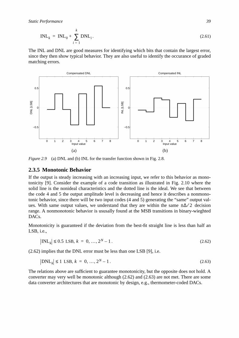
Static Performance 39
rror,raded
ono-the
tweenmono-t val-cisionhted
lf an
old. Asome
Cs.
. (2.61)
The INL and DNL are good measures for identifying which bits that contain the largest esince they then show typical behavior. They are also useful to identify the occurance of gmatching errors.
2.3.5 Monotonic BehaviorIf the output is steady increasing with an increasing input, we refer to this behavior as mtonicity [9]. Consider the example of a code transition as illustrated in Fig. 2.10 wheresolid line is the nonideal characteristics and the dotted line is the ideal. We see that bethe code 4 and 5 the output amplitude level is decreasing and hence it describes a nontonic behavior, since there will be two input codes (4 and 5) generating the “same” outpuues. With same output values, we understand that they are within the same derange. A nonmonotonic behavior is ususally found at the MSB transitions in binary-wiegDACs.
Monotonicity is guaranteed if the deviation from the best-fit straight line is less than haLSB, i.e.,
LSB, . (2.62)
(2.62) implies that the DNL error must be less than one LSB [9], i.e.
LSB, . (2.63)
The relations above are sufficient to guarantee monotonicity, but the opposite does not hconverter may very well be monotonic although (2.62) and (2.63) are not met. There aredata converter architectures that are monotonic by design, e.g., thermometer-coded DA
(a) (b)
Figure 2.9 (a) DNL and (b) INL for the transfer function shown in Fig. 2.8.
INL k INL 0 DNL ii 1=
k
∑+=
0 1 2 3 4 5 6 7 8
−0.5
0
0.5
Compensated DNL
DN
L [L
SB
]
Input value0 1 2 3 4 5 6 7 8
−0.5
0
0.5
Compensated INL
INL
[LS
B]
Input value
∆ 2⁄±
INL k 0.5≤ k 0 … 2N 1–, ,=
DNLk 1≤ k 0 … 2N 1–, ,=
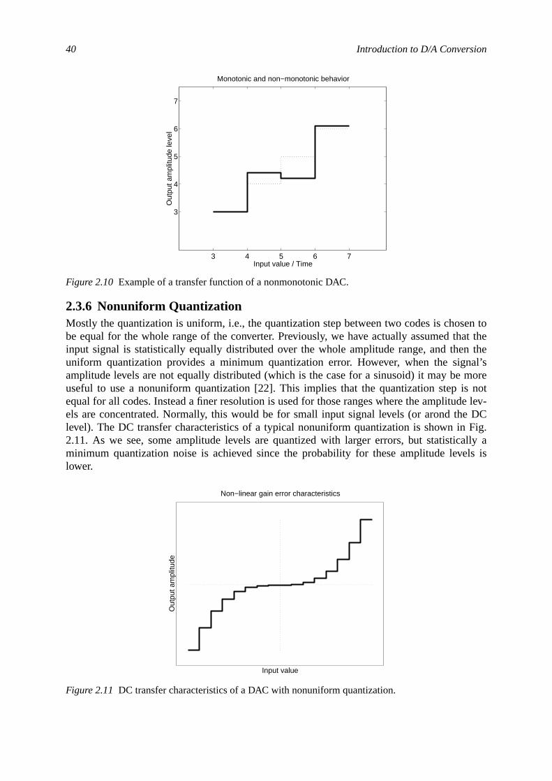
40 Introduction to D/A Conversion
en toat the
n thenal’smore
note lev-DC
Fig.ally als is
2.3.6 Nonuniform QuantizationMostly the quantization is uniform, i.e., the quantization step between two codes is chosbe equal for the whole range of the converter. Previously, we have actually assumed thinput signal is statistically equally distributed over the whole amplitude range, and theuniform quantization provides a minimum quantization error. However, when the sigamplitude levels are not equally distributed (which is the case for a sinusoid) it may beuseful to use a nonuniform quantization [22]. This implies that the quantization step isequal for all codes. Instead a finer resolution is used for those ranges where the amplitudels are concentrated. Normally, this would be for small input signal levels (or arond thelevel). The DC transfer characteristics of a typical nonuniform quantization is shown in2.11. As we see, some amplitude levels are quantized with larger errors, but statisticminimum quantization noise is achieved since the probability for these amplitude levelower.
Figure 2.10 Example of a transfer function of a nonmonotonic DAC.
Figure 2.11 DC transfer characteristics of a DAC with nonuniform quantization.
3 4 5 6 7
3
4
5
6
7
Monotonic and non−monotonic behavior
Out
put a
mpl
itude
leve
l
Input value / Time
Non−linear gain error characteristics
Out
put a
mpl
itude
Input value
Static Performance 41
, weion
itude
mini-
the
) basi-result.
Typically, we have that
(2.64)
where is the probability for the -th code to occur and
(2.65)
is the RMS quantization error and is the quantization step for the -th code. Typicallywould for uniform quantization require an equal probability, , and quantizatstep, , for all codes. We end up with the same result as in (2.28)
. (2.66)
As a notice, if the input signal is Gaussian distributed, hence the probability for the ampllevel to occur is approximately
(2.67)
where is the mean amplitude value (DC level) and is the standard deviation. Themum error power is
(2.68)
where is the quantization level for the -th code. We want to find the s that satisfyfollowing equation
, , (2.69)
which implies that
. (2.70)
(2.70) cannot be solved analytically and instead an approximation has to be done. (2.70cally expresses an inverse description of the Gaussian distribution. We can compare thiswith the case of uniformly distributed input signal, where we have for allInserting this probability in (2.70) gives the desired result
Pq εRMS2
k( ) pc k( )⋅k 0=
2N 1–
∑=
pc k( ) k
εRMS2
k( ) ∆k2 12⁄=
∆k kpc k( ) 2 N–=
∆k ∆=
Pq∆2
12------ 2 N–⋅
k 0=
2N 1–
∑ ∆2
12------= =
x
pc x( )1
σ 2π-------------- e
x µ–( )2
2σ2-------------------–
⋅≈
µ σ
Pq x qk–[ ]2 pc x( )⋅ xd
k ∆⋅
k 1+( ) ∆⋅
∫k 0=
2N 1–
∑=
qk k q
Pqd
qjd--------- 0= qj∀
qj
x pc x( )⋅ xd
j ∆⋅
j 1+( ) ∆⋅
∫
pc x( ) xd
j ∆⋅
j 1+( ) ∆⋅
∫---------------------------------------------=
pc x( ) 1 2N⁄= x
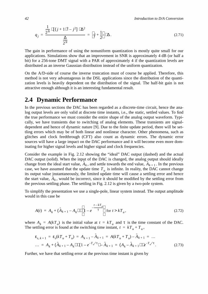
42 Introduction to D/A Conversion
ouralf aare
, thisanti-not
e ana-o find. Typi-signal-e set-ch aserrordom-
ctualallyvious
hangeence
from
litude
C.
. (2.71)
The gain in performance of using the nonuniform quantization is mostly quite small forapplications. Simulations show that an improvement in SNR is approximately 4 dB (or hbit) for a 256-tone DMT signal with a PAR of approximately 4 if the quantization levelsdistributed as an inverse Gaussian distribution instead of the uniform quantization.
On the A/D-side of course the inverse truncation must of course be applied. Thereforemethod is not very advantageous in the DSL applications since the distribution of the quzation levels is heavily dependent on the distribution of the signal. The half-bit gain isattractive enough although it is an interesting fundamental result.
2.4 Dynamic PerformanceIn the previous sections the DAC has been regarded as a discrete-time circuit, hence thlog output levels are only valid at discrete time instants, i.e., the static, settled values. Tthe true performance we must consider the entire shape of the analog output waveformcally, we have transients due to switching of analog elements. These transients aredependent and hence of dynamic nature [9]. Due to the finite update period, there will btling errors which may be of both linear and nonlinear character. Other phenomena, suglitches and clock feedthrough (CFT) also count as dynamic errors. The dynamicsources will have a large impact on the DAC performance and it will become even moreinating for higher signal levels and higher signal and clock frequencies.
Consider the example in Fig. 2.12 showing the “ideal” DAC output (dashed) and the aDAC output (solid). When the input of the DAC is changed, the analog output should idechange from the ideal start value, , and settle towards the end value, . In the precase, we have assumed that the update time is infinite. In reality, the DAC cannot cits output value instantaneously, the limited update time will cause a settling error and hthe start value, , would be incorrect, since it should be modified by the settling errorthe previous settling phase. The settling in Fig. 2.12 is given by a two-pole system.
To simplify the presentation we use a single-pole, linear system instead. The output ampwould in this case be
for , (2.72)
where is the initial value at and is the time constant of the DAThe settling error is found at the switching time instant, ,
. (2.73)
Further, we have that settling error at the previous time instant is given by
qj
12N------ j 1+( )2 j2–[ ] ∆2⋅ ⋅
∆2N------
--------------------------------------------------------- j12---+
∆⋅= =
Ak Ak 1+Tu
Ak
A t( ) Ak Ak 1+ Ak–( ) 1 e
t kTu–
τ-----------------–
–
⋅+= t kTu>
Ak A kTu( )= t kTu= τt kTu Tu+=
εs k 1+, εs kTu Tu+( ) Ak 1+ Ak 1+– A kTu Tu+( ) Ak 1+– …= = = =
… Ak Ak 1+ Ak–( ) 1 e Tu τ⁄––( )⋅ Ak 1+–+ Ak Ak 1+–( ) e Tu τ⁄–⋅= =
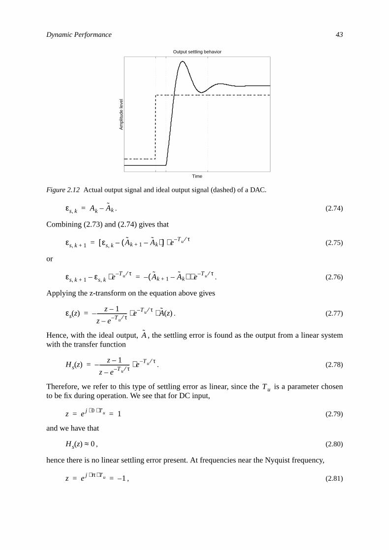
Dynamic Performance 43
stem
hosen
,
. (2.74)
Combining (2.73) and (2.74) gives that
(2.75)
or
. (2.76)
Applying the z-transform on the equation above gives
. (2.77)
Hence, with the ideal output, , the settling error is found as the output from a linear sywith the transfer function
. (2.78)
Therefore, we refer to this type of settling error as linear, since the is a parameter cto be fix during operation. We see that for DC input,
(2.79)
and we have that
, (2.80)
hence there is no linear settling error present. At frequencies near the Nyquist frequency
, (2.81)
Figure 2.12 Actual output signal and ideal output signal (dashed) of a DAC.
Output settling behavior
Am
plitu
de le
vel
Time
εs k, Ak Ak–=
εs k 1+, εs k, Ak 1+ Ak–( )–[ ] e Tu τ⁄–⋅=
εs k 1+, εs k, e Tu τ⁄–⋅– Ak 1+ Ak–( )– e Tu τ⁄–⋅=
εs z( ) z 1–
z e Tu τ⁄––-----------------------– e Tu τ⁄– A z( )⋅ ⋅=
A
Hs z( ) z 1–
z e Tu τ⁄––-----------------------– e Tu τ⁄–⋅=
Tu
z ej 0 Tu⋅ ⋅ 1= =
Hs z( ) 0≈
z ej π Tu⋅ ⋅ 1–= =
44 Introduction to D/A Conversion
lin-nal-
thatar set-the set-usednd isd it is
sible.
shapechesue toignal.a sig-
ufferthe
s sen-h SR
that
thee timeof theeriva-
ge
we have the maximum value given by
. (2.82)
These issues are also further discussed in Sec. 4.3.1.
In reality, the actual start and final values, and , will not only be modified by theear settling errors. They will also be influenced by circuit imperfections, glitches, sigdependent time constants , etc.
The required settling time is usually larger for larger output steps. The reason for this isthe settling usually can be divided into two phases, a nonlinear slewing phase and a linetling phase. The slewing phase should be as small as possible since it both increasestling time and introduces distortion in the analog waveform. The slewing is normally caby a too small bias current in the circuit driving the output, e.g., output voltage buffers, atherefore higher for large steps since more current is needed. Distortion is introduced antherefore important to try to keep the nonlinear portion of the settling as small as posThis is further discussed in Sec. 2.4.1.
There are additional dynamic error sources that can both change the final value and theof the settling waveform, as for instance glitches and clock feedthrough (CFT) [7]. Glitdepend on how the internal switches are individually skewed in time and CFT arises dthe capacitive coupling between the digital switching signal and the analog output sAnother dynamic error is the sampling-time uncertainty, which can be considered to benal-dependent settling error.
2.4.1 Nonlinear SettlingFor example, the current-steering DAC without output buffers (Sec. 3.6.1) does not sfrom slew rate limiting, but on the other hand it is much more sensitive to the variations inoutput impedance. Using output buffers in this DAC architecture makes the converter lessitive to limited output impedance, but on the other hand, we now have the problem witlimiting and the increased circuit complexity.
Typically, the SR is limited by the achievable, maximum slope of the output. Assumingthe output is described by a voltage level, we have that
, (2.83)
where is the maximum current that can be directed to the output and iscapacitive load associated with the output. For linear settling, we must guarantee that thconstant of the system is signal-independent and that the SR is not limiting the slopeoutput signal. For a linear, single-pole system, (2.72), the largest slope is given by the dtive of the output signal at the initial time instant, hence
. (2.84)
Although it might not be likely for low signal-to-clock frequency ratios, the maximum chan
Hs z( ) 2
1 e Tu τ⁄–+------------------------– e Tu τ⁄–⋅=
Ak Ak 1+
τ τ t( )=
SRdVout t( )
dt--------------------
tmax
iout t( )
CL--------------
tmax
1CL------ iout t( )
tmax⋅
I out max,CL
-------------------= = = =
I out max, CL
dVout t( )
dt--------------------
tmax
Ak 1+ Ak–
τ----------------------------
tmax
1τ--- Ak 1+ Ak–
tmax⋅= =
Dynamic Performance 45
hed.weenfalse
ansi-
shortout-epen-signal
di-pulse
. The
of amplitude could be rail-to-rail, and we would get
. (2.85)
We should for worst-case settling require that
. (2.86)
Using (2.83) in (2.86) gives
. (2.87)
For the current-steering DAC architecture without buffers, we have that
. (2.88)
The time constant is likely to be determined by the load impedance and hence given by
. (2.89)
The comparison in (2.87) becomes for the current-steering DAC
(2.90)
which states that there is no slew-rate limiting for this architecture.
2.4.2 GlitchesGlitches occur when the switching time instants of different bits in a DAC are unmatcThis can depend on matching errors in switches and driver circuits, time skew betswitching signals, voltage-dependent CMOS switches, etc. For a short period of time acode could appear at the output. For example, in a binary-weighted DAC, if the code trtion is
and the MSB is switching faster than the LSBs, the code may be present for aperiod of time. This is a major code transition and the DAC will represent the maximumput value and hence a large glitch will appear at the output. The glitch adds a signal-ddent error to the output signal, that degrades the performance. The impact on the outputcan be characterized by the average energy or power of the glitches.
In Fig. 2.13 we illustrate the typical glitch behavior at the DAC output. The dotted line incates the ideal transfer and the solid line the actual behavior. The glitch is modeled as aas dashed in the figure. This pulse has an amplitude of and a time-duration,glitch energy during the time interval is given by
dVout t( )
dt--------------------
tmax
1τ--- 2N ∆⋅ ⋅≈
SR1τ--- 2N ∆⋅ ⋅≥
I out max,CL
------------------- 1τ--- 2N ∆⋅ ⋅≥
∆I out max,
2N------------------- RL⋅=
τ RL CL⋅=
I out max,CL
------------------- 1RL CL⋅----------------- 2N
I out max,
2N------------------- RL⋅ ⋅ ⋅≥
I out max,CL
-------------------=
0111…111 1000…000→
11…111
Ag k, Tg k,kTu t k 1+( )Tu≤ ≤
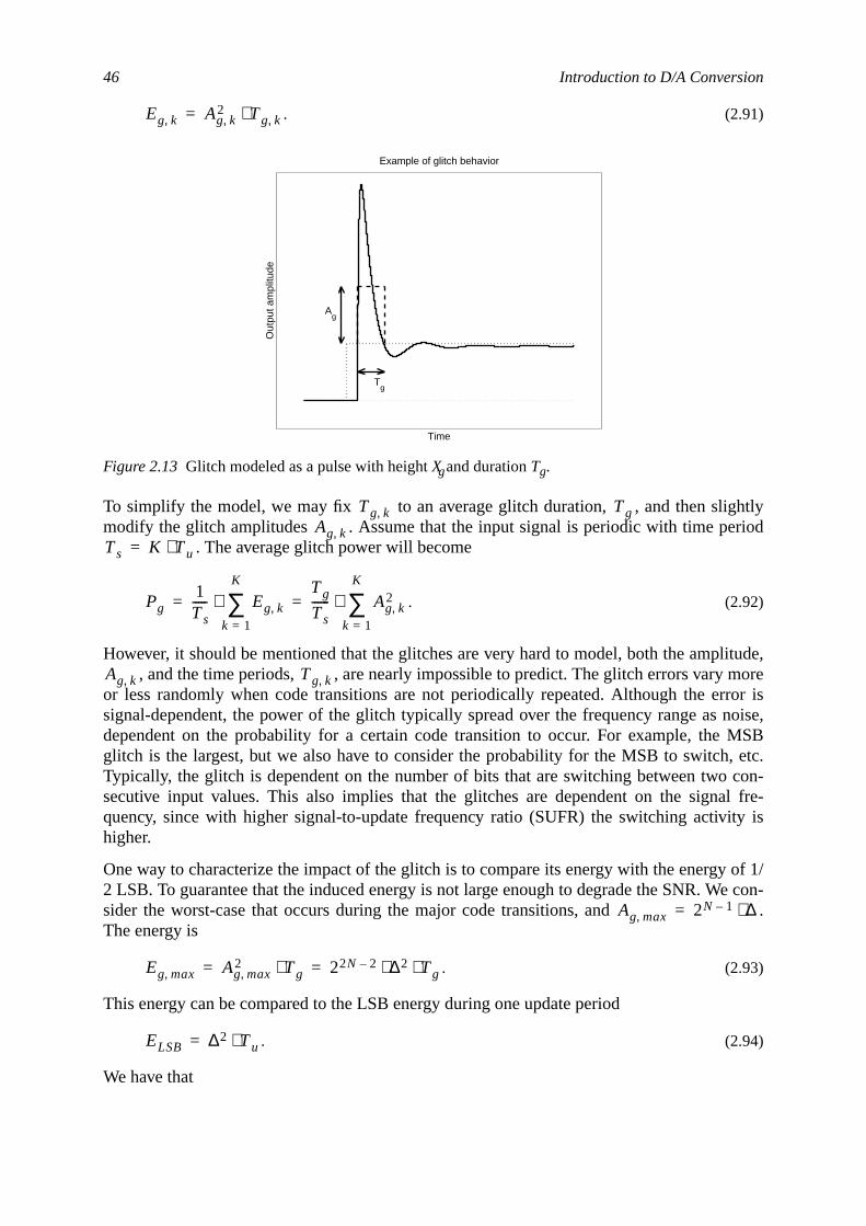
46 Introduction to D/A Conversion
htlyriod
itude,ore
ror isnoise,MSBetc.con-l fre-
ty is
of 1/e con-
.
. (2.91)
To simplify the model, we may fix to an average glitch duration, , and then sligmodify the glitch amplitudes . Assume that the input signal is periodic with time pe
. The average glitch power will become
. (2.92)
However, it should be mentioned that the glitches are very hard to model, both the ampl, and the time periods, , are nearly impossible to predict. The glitch errors vary m
or less randomly when code transitions are not periodically repeated. Although the ersignal-dependent, the power of the glitch typically spread over the frequency range asdependent on the probability for a certain code transition to occur. For example, theglitch is the largest, but we also have to consider the probability for the MSB to switch,Typically, the glitch is dependent on the number of bits that are switching between twosecutive input values. This also implies that the glitches are dependent on the signaquency, since with higher signal-to-update frequency ratio (SUFR) the switching activihigher.
One way to characterize the impact of the glitch is to compare its energy with the energy2 LSB. To guarantee that the induced energy is not large enough to degrade the SNR. Wsider the worst-case that occurs during the major code transitions, andThe energy is
. (2.93)
This energy can be compared to the LSB energy during one update period
. (2.94)
We have that
Figure 2.13 Glitch modeled as a pulse with heightXg and durationTg.
Eg k, Ag k,2 Tg k,⋅=
Ag
Tg
Example of glitch behavior
Out
put a
mpl
itude
Time
Tg k, TgAg k,
Ts K Tu⋅=
Pg1Ts----- Eg k,
k 1=
K
∑⋅Tg
Ts------ Ag k,
2
k 1=
K
∑⋅= =
Ag k, Tg k,
Ag max, 2N 1– ∆⋅=
Eg max, Ag max,2 Tg⋅ 22N 2– ∆2 Tg⋅ ⋅= =
ELSB ∆2 Tu⋅=
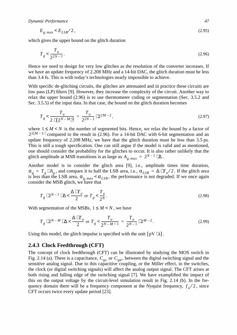
Dynamic Performance 47
es. Ifless
ts arey to.2 and
tor ofan
.5 ps.ned,t the
ion,eaagain
h ind thehes,s att offre-since
, (2.95)
which gives the upper bound on the glitch duration
. (2.96)
Hence we need to design for very low glitches as the resolution of the converter increaswe have an update frequency of 2.208 MHz and a 14-bit DAC, the glitch duration must bethan 3.4 fs. This is with today’s technologies nearly impossible to achieve.
With specific de-glitching circuits, the glitches are attenuated and in practice these circuilow pass (LP) filters [9]. However, they increase the complexity of the circuit. Another warelax the upper bound (2.96) is to use thermometer coding or segmentation (Sec. 3.5Sec. 3.5.5) of the input data. In that case, the bound on the glitch duration becomes
, (2.97)
where is the number of segmented bits. Hence, we relax the bound by a faccompared to the result in (2.96). For a 14-bit DAC with 6-bit segmentation and
update frequency of 2.208 MHz, we have that the glitch duration must be less than 3This is still a tough specification. One can still argue if the model is valid and as mentioone should consider the probability for the glitches to occur. It is also rather unlikely thaglitch amplitude at MSB transitions is as large as .
Another model is to consider the glitch area [9], i.e., amplitude times time durat, and compare it to half the LSB area, i.e., . If the glitch ar
is less than the LSB area, , the performance is not degraded. If we onceconsider the MSB glitch, we have that
or . (2.98)
With segmentation of the MSBs, , we have
or . (2.99)
Using this model, the glitch impulse is specified with the unit .
2.4.3 Clock Feedthrough (CFT)The concept of clock feedthrough (CFT) can be illustrated by studying the MOS switcFig. 2.14 (a). There is a capacitance, or , between the digital switching signal ansensitive analog signal. Due to this capacitive coupling, or the Miller effect, in the switcthe clock (or digital switching signals) will affect the analog output signal. The CFT ariseboth rising and falling edge of the switching signal [7]. We have examplified the impacthis on the output voltage by the circuit-level simulation result in Fig. 2.14 (b). In thequency domain there will be a frequency component at the Nyquist frequency, ,CFT occurs twice every update period [23].
Eg max, ELSB 2⁄<
Tg
Tu
22N 1–---------------<
Tg
Tu
2 2N M–( )2⋅------------------------------<
Tu
22N 1–--------------- 22M 2–⋅=
1 M≤ N<22 M 1–( )
Ag max, 2N 1– ∆⋅=
αg Tg Ag⋅= αLSB ∆ Tu⋅ 2⁄=αg max, αLSB<
Tg 2N 1– ∆⋅ ⋅∆ Tu⋅
2--------------< Tg
Tu
2N------<
1 M N<≤
Tg 2N M– ∆⋅ ⋅∆ Tu⋅
2--------------< Tg
Tu
2N M– 1+----------------------<
Tu
2N 1–------------- 2M 2–⋅=
pV s⋅[ ]
Cgs Cgd
f u 2⁄
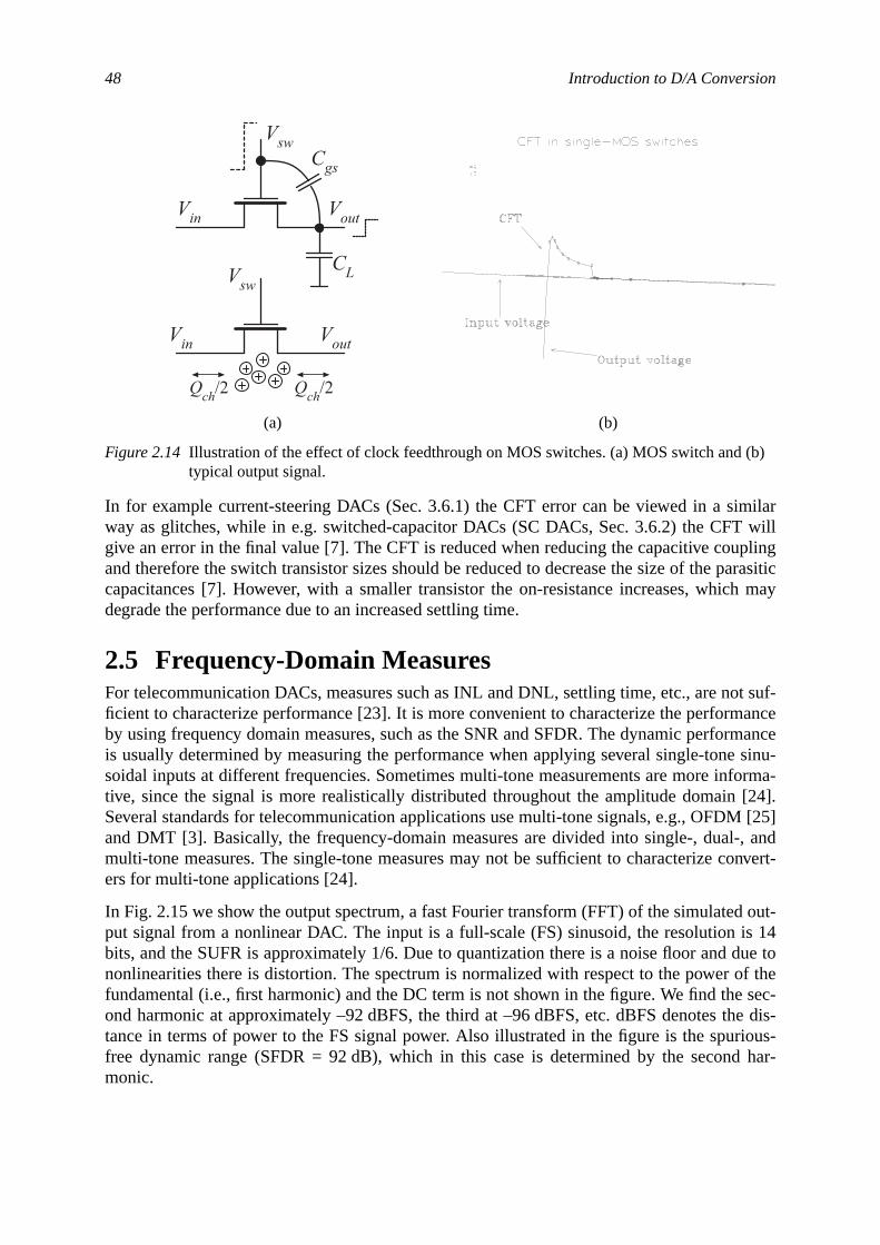
48 Introduction to D/A Conversion
milarwill
plingarasitich may
t suf-ance
mancesinu-
forma-[24].
[25], andonvert-
out-s 14ue tof thesec-e dis-ious-
har-
(b)
In for example current-steering DACs (Sec. 3.6.1) the CFT error can be viewed in a siway as glitches, while in e.g. switched-capacitor DACs (SC DACs, Sec. 3.6.2) the CFTgive an error in the final value [7]. The CFT is reduced when reducing the capacitive couand therefore the switch transistor sizes should be reduced to decrease the size of the pcapacitances [7]. However, with a smaller transistor the on-resistance increases, whicdegrade the performance due to an increased settling time.
2.5 Frequency-Domain MeasuresFor telecommunication DACs, measures such as INL and DNL, settling time, etc., are noficient to characterize performance [23]. It is more convenient to characterize the performby using frequency domain measures, such as the SNR and SFDR. The dynamic perforis usually determined by measuring the performance when applying several single-tonesoidal inputs at different frequencies. Sometimes multi-tone measurements are more intive, since the signal is more realistically distributed throughout the amplitude domainSeveral standards for telecommunication applications use multi-tone signals, e.g., OFDMand DMT [3]. Basically, the frequency-domain measures are divided into single-, dual-multi-tone measures. The single-tone measures may not be sufficient to characterize cers for multi-tone applications [24].
In Fig. 2.15 we show the output spectrum, a fast Fourier transform (FFT) of the simulatedput signal from a nonlinear DAC. The input is a full-scale (FS) sinusoid, the resolution ibits, and the SUFR is approximately 1/6. Due to quantization there is a noise floor and dnonlinearities there is distortion. The spectrum is normalized with respect to the power ofundamental (i.e., first harmonic) and the DC term is not shown in the figure. We find theond harmonic at approximately –92 dBFS, the third at –96 dBFS, etc. dBFS denotes thtance in terms of power to the FS signal power. Also illustrated in the figure is the spurfree dynamic range (SFDR = 92 dB), which in this case is determined by the secondmonic.
(a) (b)
Figure 2.14 Illustration of the effect of clock feedthrough on MOS switches. (a) MOS switch and typical output signal.
Cgs
CL
Vsw
Vin Vout
Vin Vout
Vsw
Qch/2 Qch/2
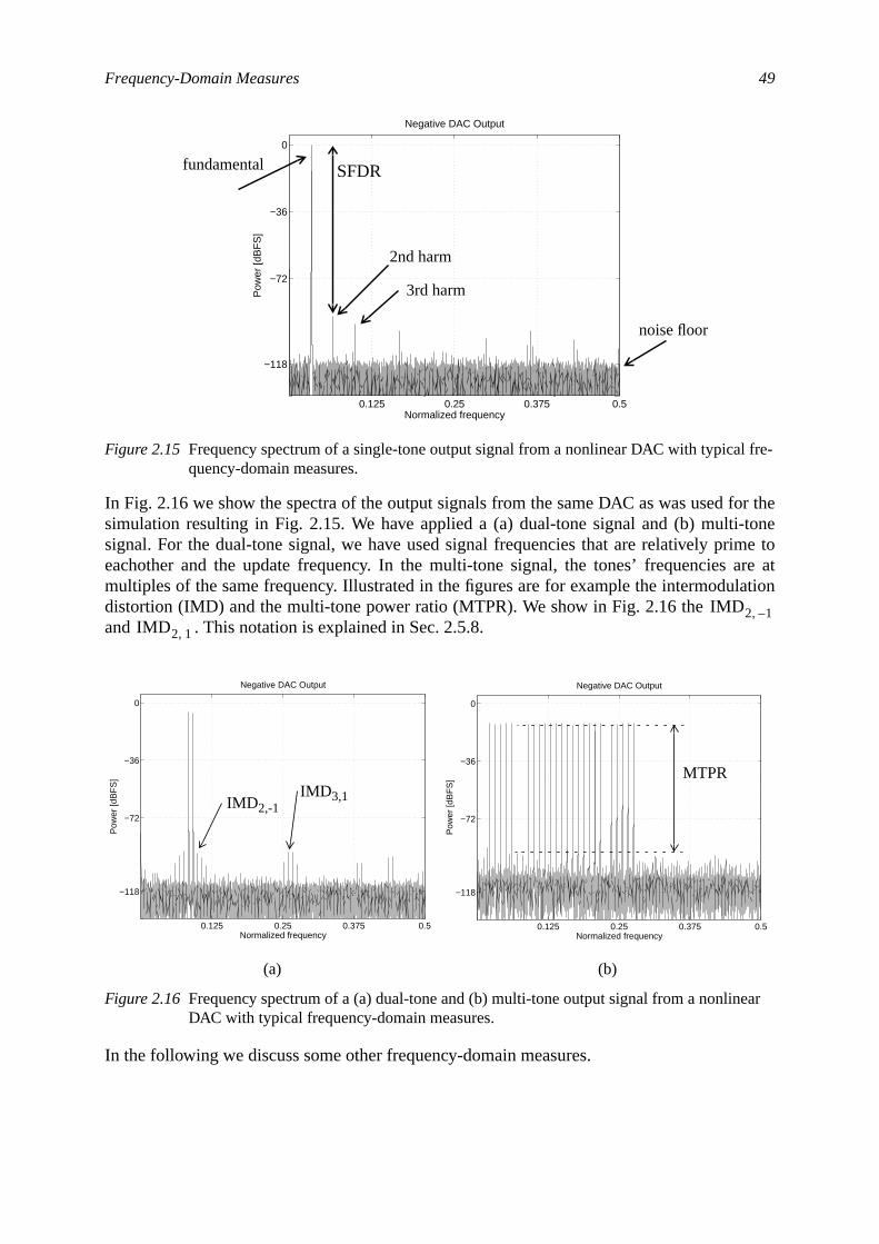
Frequency-Domain Measures 49
or thetoneme toare atlation
l fre-
ear
In Fig. 2.16 we show the spectra of the output signals from the same DAC as was used fsimulation resulting in Fig. 2.15. We have applied a (a) dual-tone signal and (b) multi-signal. For the dual-tone signal, we have used signal frequencies that are relatively prieachother and the update frequency. In the multi-tone signal, the tones’ frequenciesmultiples of the same frequency. Illustrated in the figures are for example the intermodudistortion (IMD) and the multi-tone power ratio (MTPR). We show in Fig. 2.16 theand . This notation is explained in Sec. 2.5.8.
In the following we discuss some other frequency-domain measures.
Figure 2.15 Frequency spectrum of a single-tone output signal from a nonlinear DAC with typicaquency-domain measures.
(a) (b)
Figure 2.16 Frequency spectrum of a (a) dual-tone and (b) multi-tone output signal from a nonlinDAC with typical frequency-domain measures.
0.125 0.25 0.375 0.5
−118
−72
−36
0
Negative DAC Output
Normalized frequency
Pow
er [d
BF
S]
SFDR
2nd harm
3rd harm
noise floor
fundamental
IMD 2 1–,IMD 2 1,
0.125 0.25 0.375 0.5
−118
−72
−36
0
Negative DAC Output
Normalized frequency
Pow
er [d
BF
S]
IMD2,-1IMD3,1
0.125 0.25 0.375 0.5
−118
−72
−36
0
Negative DAC Output
Normalized frequency
Pow
er [d
BF
S] MTPR

50 Introduction to D/A Conversion
een
oidand
the
oidnicss no5 is
total
also
ntal
03) in
2.5.1 Harmonic Distortion (HDk)
The harmonic distortion with respect to the -th harmonic, , is the power ratio betwthe -th harmonic and the fundamental
(2.100)
where is the power of the fundamental (typically the signal, , for a sinusinput). is the power of the -th harmonic. For example, we have that dB
dB for the signal in Fig. 2.15.
2.5.2 Total Harmonic Distortion (THD)The total harmonic distortion (THD) is the ratio of the total harmonic distortion power andpower of the fundamental in a certain frequency band, i.e.,
(2.101)
where is the power of the fundamental (typically the signal, , for a sinusinput). is the power of the -th harmonic. Since there is an infinite number of harmothe THD is usually calculated using the first 10–20 harmonics or until the harmoniclonger can be distinguished from the noise floor [26]. The THD for the signal in Fig. 2.1approximately 89 dB.
2.5.3 Signal-to-Noise Ratio (SNR)The signal-to-noise ratio (SNR) is the ratio of the power of the fundamental and thenoise power within a certain frequency band, excluding the harmonic components, i.e.,
(2.102)
where is the signal power and is the noise power. The SNR is sometimesexpressed in dBFS to relate the noise level to the full-scale input power.
2.5.4 Signal-to-Noise and Distortion Ratio (SNDR)The signal-to-noise-and-distortion ratio (SNDR) is the ratio of the power of the fundameand the total noise and distortion power within a certain frequency band, i.e.,
(2.103)
The SNDR is also sometimes expressed in dBFS. Expressing (2.101), (2.102), and (2.1a linear scale gives the obvious relation
. (2.104)
The SNDR of the signal in Fig. 2.15 is approximately 85 dB.
k HDkk
HDk 10Pk
P1------log10⋅=
P1 Ps P1=Pk k HD2 92≈
HD3 96≈
THD 10Pkk 2=
∞∑P1
-----------------------log10⋅ 10Pk
P1------
k 2=
∞
∑log10⋅= =
P1 Ps P1=Pk k
SNR 10Ps
Pn------log10⋅=
Ps Pn
SNDR 10Ps
Pn Pkk 2=
∞∑+-----------------------------------log10⋅=
SNDR SNR THD+=
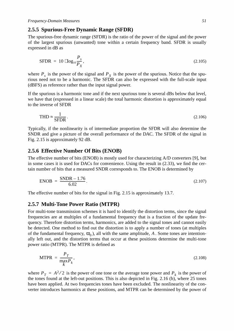
Frequency-Domain Measures 51
owerually
spu-input
level,equal
theal in
butcer-
ignale fre-t easilyltiplestion-
-tone
er oftonese con-wer of
2.5.5 Spurious-Free Dynamic Range (SFDR)The spurious-free dynamic range (SFDR) is the ratio of the power of the signal and the pof the largest spurious (unwanted) tone within a certain frequency band. SFDR is usexpressed in dB as
, (2.105)
where is the power of the signal and is the power of the spurious. Notice that therious need not to be a harmonic. The SFDR can also be expressed with the full-scale(dBFS) as reference rather than the input signal power.
If the spurious is a harmonic tone and if the next spurious tone is several dBs below thatwe have that (expressed in a linear scale) the total harmonic distortion is approximatelyto the inverse of SFDR
. (2.106)
Typically, if the nonlinearity is of intermediate proportion the SFDR will also determineSNDR and give a picture of the overall performance of the DAC. The SFDR of the signFig. 2.15 is approximately 92 dB.
2.5.6 Effective Number Of Bits (ENOB)The effective number of bits (ENOB) is mostly used for characterizing A/D converters [9],in some cases it is used for DACs for convenience. Using the result in (2.33), we find thetain number of bits that a measured SNDR corresponds to. The ENOB is determined by
. (2.107)
The effective number of bits for the signal in Fig. 2.15 is approximately 13.7.
2.5.7 Multi-Tone Power Ratio (MTPR)For multi-tone transmission schemes it is hard to identify the distortion terms, since the sfrequencies are at multiples of a fundamental frequency that is a fraction of the updatquency. Therefore distortion terms, harmonics, are added to the signal tones and cannobe detected. One method to find out the distortion is to apply a number of tones (at muof the fundamental frequency, ), all with the same amplitude, . Some tones are intenally left out, and the distortion terms that occur at these positions determine the multipower ratio (MTPR). The MTPR is defined as
, (2.108)
where is the power of one tone or the average tone power and is the powthe tones found at the left-out positions. This is also depicted in Fig. 2.16 (b), where 25have been applied. At two frequencies tones have been excluded. The nonlinearity of thverter introduces harmonics at these positions, and MTPR can be determined by the po
SFDR 10Ps
PX------log10⋅=
Ps PX
THD1
SFDR---------------≈
ENOB SNDR 1.76–6.02
--------------------------------=
ω0 A
MTPRPT
Pkkmax----------------=
PT A2 2⁄= Pk
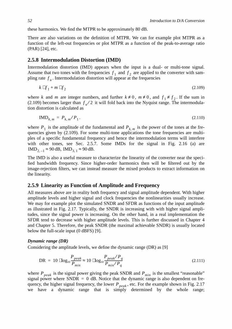
52 Introduction to D/A Conversion
as aratio
nal.sam-
inula-
fre-multi-rfereare
speci-the
on on
igherrease.itudepli-n the
pter 4cated
ble”fre-
2.17nge;
these harmonics. We find the MTPR to be approximately 80 dB.
There are also variations on the definition of MTPR. We can for example plot MTPRfunction of the left-out frequencies or plot MTPR as a function of the peak-to-average(PAR) [24], etc.
2.5.8 Intermodulation Distortion (IMD)Intermodulation distortion (IMD) appears when the input is a dual- or multi-tone sigAssume that two tones with the frequencies and are applied to the converter withpling rate . Intermodulation distortion will appear at the frequencies
(2.109)
where and are integer numbers, and further , , and . If the sum(2.109) becomes larger than it will fold back into the Nyquist range. The intermodtion distortion is calculated as
. (2.110)
where is the amplitude of the fundamental and is the power of the tones at thequencies given by (2.109). For some multi-tone applications the tone frequencies areples of a specific fundamental frequency and hence the intermodulation terms will intewith other tones, see Sec. 2.5.7. Some IMDs for the signal in Fig. 2.16 (a)
dB, dB.
The IMD is also a useful measure to characterize the linearity of the converter near thefied bandwidth frequency. Since higher-order harmonics then will be filtered out byimage-rejection filters, we can instead measure the mixed products to extract informatithe linearity.
2.5.9 Linearity as Function of Amplitude and FrequencyAll measures above are in reality both frequency and signal amplitude dependent. With hamplitude levels and higher signal and clock frequencies the nonlinearities usually incWe may for example plot the simulated SNDR and SFDR as functions of the input amplas illustrated in Fig. 2.17. Typically, the SNDR is increasing with with higher signal amtudes, since the signal power is increasing. On the other hand, in a real implementatioSFDR tend to decrease with higher amplitude levels. This is further discussed in Chaand Chapter 5. Therefore, the peak SNDR (the maximal achievable SNDR) is usually lobelow the full-scale input (0 dBFS) [9].
Dynamic range (DR)Considering the amplitude levels, we define the dynamic range (DR) as [9]
(2.111)
where is the signal power giving the peak SNDR and is the smallest “reasonasignal power where dB. Notice that the dynamic range is also dependent onquency, the higher signal frequency, the lower , etc. For the example shown in Fig.we have a dynamic range that is simply determined by the whole ra
f 1 f 2f u
k f 1⋅ m f2⋅+
k m k 0≠ m 0≠ f 1 f 2≠f u 2⁄
IMD k m, Pk m, P1⁄=
P1 Pk m,
IMD 2 1–, 90≈ IMD 3 1, 90≈
DR 10Ppeak
Pmin-------------log10⋅ 10
Ppeak Pq⁄Pmin Pq⁄-----------------------log10⋅≈=
Ppeak PminSNDR 0=
Ppeak
Frequency-Domain Measures 53
quencyt theshowcy forhar-R is
grades.
dB.
Effective resolution bandwidth (ERB)Since the measures are frequency-dependent we must also be careful to specify the frerange in which for example a certain SFDR can be guaranteed. It is common to ploSFDR, SNDR, or SNR as function of the SUFR and update frequency. In Fig. 2.18 wethe measured SFDR for a 14-bit current-steering DAC as function of the update frequentwo SUFR, 0.03 and 0.06. The effective resolution bandwidth (ERB) is mostly used for cacterization of A/D converters and is defined as the input frequency where the SNDreduced by 3 dB (or ENOB by half a bit) [9].
The slope of the curves are also interesting since they describe how the performance deIn the figure this slope is approximately 17 dB per decade.
Figure 2.17 Typical SNDR and SFDR vs. amplitude level for a 14-bit DAC.
Figure 2.18 Measured SFDR as function of update and signal frequencies.
−24 −18 −12 −6 −3 0
48
60
72
84
SFDR and SNDR vs. amplitude level
Amplitude level [dBFS]
SN
DR
, SF
DR
[dB
]
SFDR
SNDR
6.02 N⋅ 1.76+ 86≈
5 12.5 25 50 100
50
60
70
SUFR = 0.03
SUFR = 0.06
Measured SFDR vs. update frequency. DAC A and C.
Update frequency [MHz]
SF
DR
[dB
]
54 Introduction to D/A Conversion
addi-nals.gnalvan-
ve we
mu-use thecon-
rting
2.5.10 Peak-to-Average Ratio (PAR)For multi-tone transmission we use the peak-to-average ratio (PAR) or crest factor as antional signal characterization [23, 24]. In Sec. 1.3.2 we discussed the PAR for DMT sigWith the PAR value we get additional information on how the amplitude levels of the siare distributed. Low PAR indicates a more uniform distribution, which in most cases is adtageous. The PAR is defined as
, (2.112)
where is the peak signal power and is the average signal power. For a sine wahave
. (2.113)
Typically, a sine wave input signal is used for testing converters, but in most practical comnications applications more than one tone are used in the signals. In those cases, wePAR to calculate the SNR. Assuming that the peak signal is FS, the PAR for an -bitverter is
. (2.114)
From (2.114) the average signal power, , is
. (2.115)
Further, the SNR (with respect to the quantization noise) is given by (2.33) and inse(2.115) gives
dB. (2.116)
We see from (2.116) that a small PAR is preferable since it maximizes the SNR.
PARPpeak
Ps-------------
1 2/=
Ppeak Ps
PARA2
A2 2⁄-------------
1 2/2= =
N
PARPpeak
Ps-------------
1 2/ ∆ 2N 1–⋅( )2
Ps-----------------------------
1 2/≈=
Ps
Ps∆ 2N 1–⋅
PAR---------------------
2=
SNR 10Ps
Pq------log10⋅ 10
∆ 2N 1–⋅PAR
---------------------2
∆2 12⁄-----------------------------log10⋅ ≈= =
6.02 N 20 PARlog10⋅– 4.77+⋅≈
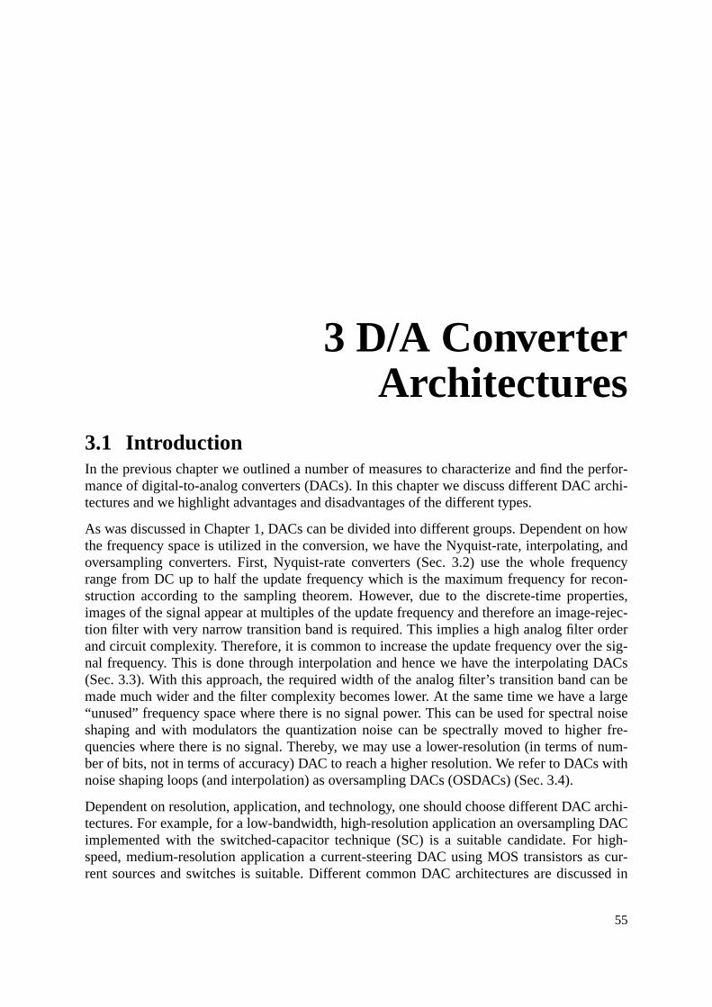
erfor-rchi-
n how, and
uencycon-rties,-rejec-dere sig-
ACsn belargel noiser fre-num-with
archi-DAChigh-s cur-sed in
3 D/A ConverterArchitectures
3.1 IntroductionIn the previous chapter we outlined a number of measures to characterize and find the pmance of digital-to-analog converters (DACs). In this chapter we discuss different DAC atectures and we highlight advantages and disadvantages of the different types.
As was discussed in Chapter 1, DACs can be divided into different groups. Dependent othe frequency space is utilized in the conversion, we have the Nyquist-rate, interpolatingoversampling converters. First, Nyquist-rate converters (Sec. 3.2) use the whole freqrange from DC up to half the update frequency which is the maximum frequency for restruction according to the sampling theorem. However, due to the discrete-time propeimages of the signal appear at multiples of the update frequency and therefore an imagetion filter with very narrow transition band is required. This implies a high analog filter orand circuit complexity. Therefore, it is common to increase the update frequency over thnal frequency. This is done through interpolation and hence we have the interpolating D(Sec. 3.3). With this approach, the required width of the analog filter’s transition band camade much wider and the filter complexity becomes lower. At the same time we have a“unused” frequency space where there is no signal power. This can be used for spectrashaping and with modulators the quantization noise can be spectrally moved to highequencies where there is no signal. Thereby, we may use a lower-resolution (in terms ofber of bits, not in terms of accuracy) DAC to reach a higher resolution. We refer to DACsnoise shaping loops (and interpolation) as oversampling DACs (OSDACs) (Sec. 3.4).
Dependent on resolution, application, and technology, one should choose different DACtectures. For example, for a low-bandwidth, high-resolution application an oversamplingimplemented with the switched-capacitor technique (SC) is a suitable candidate. Forspeed, medium-resolution application a current-steering DAC using MOS transistors arent sources and switches is suitable. Different common DAC architectures are discus
55
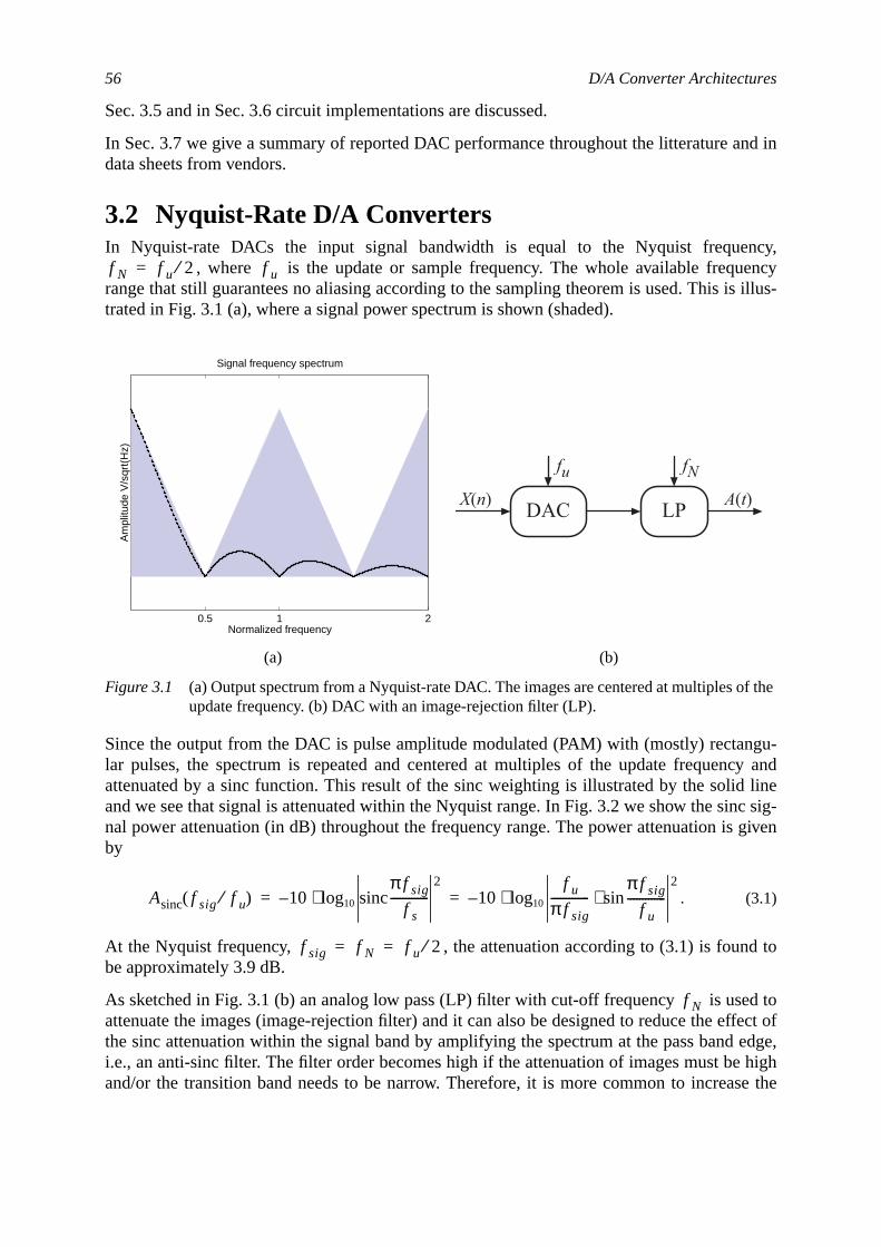
56 D/A Converter Architectures
nd in
ncy,ency
illus-
gu-cy andlinec sig-given
to
d toffect ofedge,high
se the
f the
Sec. 3.5 and in Sec. 3.6 circuit implementations are discussed.
In Sec. 3.7 we give a summary of reported DAC performance throughout the litterature adata sheets from vendors.
3.2 Nyquist-Rate D/A ConvertersIn Nyquist-rate DACs the input signal bandwidth is equal to the Nyquist freque
, where is the update or sample frequency. The whole available frequrange that still guarantees no aliasing according to the sampling theorem is used. This istrated in Fig. 3.1 (a), where a signal power spectrum is shown (shaded).
Since the output from the DAC is pulse amplitude modulated (PAM) with (mostly) rectanlar pulses, the spectrum is repeated and centered at multiples of the update frequenattenuated by a sinc function. This result of the sinc weighting is illustrated by the solidand we see that signal is attenuated within the Nyquist range. In Fig. 3.2 we show the sinnal power attenuation (in dB) throughout the frequency range. The power attenuation isby
. (3.1)
At the Nyquist frequency, , the attenuation according to (3.1) is foundbe approximately 3.9 dB.
As sketched in Fig. 3.1 (b) an analog low pass (LP) filter with cut-off frequency is useattenuate the images (image-rejection filter) and it can also be designed to reduce the ethe sinc attenuation within the signal band by amplifying the spectrum at the pass bandi.e., an anti-sinc filter. The filter order becomes high if the attenuation of images must beand/or the transition band needs to be narrow. Therefore, it is more common to increa
(a) (b)
Figure 3.1 (a) Output spectrum from a Nyquist-rate DAC. The images are centered at multiples oupdate frequency. (b) DAC with an image-rejection filter (LP).
f N f u 2⁄= f u
0.5 1 2
Signal frequency spectrum
Am
plitu
de V
/sqr
t(H
z)
Normalized frequency
DAC LP A(t)X(n)
fu fN
Asinc f sig f u⁄( ) 10–π f sig
f s-------------sinc
2log10⋅ 10–
f u
π f sig-------------
π f sig
f u-------------sin⋅
2log10⋅= =
f sig f N f u 2⁄= =
f N
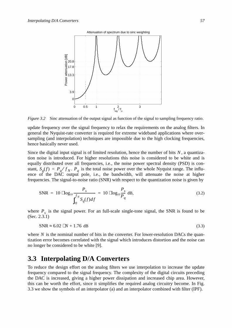
Interpolating D/A Converters 57
rs. Inover-
ncies,
tiza-nd iscon-
flu-gheren by
o be
uan-e can
pdatedingever,Fig.PF).
atio.
update frequency over the signal frequency to relax the requirements on the analog filtegeneral the Nyquist-rate converter is required for extreme wideband applications wheresampling (and interpolation) techniques are impossible due to the high clocking frequehence basically never used.
Since the digital input signal is of limited resolution, hence the number of bits , a quantion noise is introduced. For higher resolutions this noise is considered to be white aequally distributed over all frequencies, i.e., the noise power spectral density (PSD) isstant, . is the total noise power over the whole Nyquist range. The inence of the DAC output pole, i.e., the bandwidth, will attenuate the noise at hifrequencies. The signal-to-noise ratio (SNR) with respect to the quantization noise is giv
dB, (3.2)
where is the signal power. For an full-scale single-tone signal, the SNR is found t(Sec. 2.3.1)
dB (3.3)
where is the nominal number of bits in the converter. For lower-resolution DACs the qtization error becomes correlated with the signal which introduces distortion and the noisno longer be considered to be white [9].
3.3 Interpolating D/A ConvertersTo reduce the design effort on the analog filters we use interpolation to increase the ufrequency compared to the signal frequency. The complexity of the digital circuits precethe DAC is increased, giving a higher power dissipation and increased chip area. Howthis can be worth the effort, since it simplifies the required analog circuitry become. In3.3 we show the symbols of an interpolator (a) and an interpolator combined with filter (I
Figure 3.2 Sinc attenuation of the output signal as function of the signal to sampling frequency r
0 0.5 1 2 3
0
3.9
13.3
17.8
20.8
fsig
/ fu
Pow
er a
ttenu
atio
n [d
B]
Attenuation of spectrum due to sinc weighting
N
Sq f( ) Pq f N⁄= Pq
SNR 10Ps
Sq f( ) fd0
f N
∫----------------------------log10⋅ 10
Ps
Pq------log10⋅= =
Ps
SNR 6.02 N⋅ 1.76+≈
N
58 D/A Converter Architectures
tion
rpo-used.
datencythe
on-howin theig. 3.4po-ana-
t-of-up toh an, forents.
)z to
am-
ite-plex,
sitionlter
o theedge
IFIR)tion
The input signal of the interpolator is padded with zeros which corresponds to the opera
, (3.4)
where is the rate (or order) of the interpolation and is an integer. Typically, the intelation is done in a multi-stage configuration, hence several cascaded interpolators areWe will refer to the total interpolation rate as the oversampling ratio (OSR). The new upfrequency of the DAC is denoted and the corresponding Nyquist frequeis . Notice, that the Nyquist-rate DAC is defined to have OSR = 1. Infrequency domain, the operation in (3.4) corresponds to
, (3.5)
hence, the spectrum will repeat itself times in the frequency range up to . Csider the example in Fig. 3.4 where an interpolation of order 4 is illustrated. In (a) we sthe original signal spectrum and (b) illustrates how the signal spectrum is repeated withfrequency range. These images are attenuated by the digital filters. The dashed line in F(b) shows the corresponding ideal filtering function. In Fig. 3.4 (c) we find the final interlated signal and the dotted line in the figure illustrates the transition band of the requiredlog filters at the output. The transition band is now in the order of .
The specification on the interpolation filters is given by the required attenuation of ouband signals. As an example, we assume that a ripple of 1 dB within the passband1.104 MHz is allowed and a attenuation of 60 dB for frequencies above 2.208 MHz. Witoversampling ratio of 1, this specification must be met with analog filters only. However
we use the digital interpolation filters to relax the design of the analog componUsing the specification above and applying it on the digital domain, we have (forthat 1.104 MHz corresponds to the normalized angular frequency and 2.208 MH
. In Table 3.1 we show some different required filter orders for different overspling ratios and filter structures.
The infinite-length impulse response (IIR) filters have a lower filter order than the finlength impulse response (FIR) filters. However, the design of the IIR filters is more comsince a larger effort has to be put on designing them for stability, round-off noise, etc.
For high oversampling ratios, the interpolation filters must be designed for a narrow tranband. In a single-stage interpolator, this will often require a high filter order and long ficoefficients. With halfband filters the number of nonzero coefficients can be reduced thalf. The drawback with halfband filters, though, is that the attenuation at the passbandis 3 dB. Some special frequency masking techniques with for example interpolated FIR (filters or similar are also applicable to reduce the overall complexity. More on interpola
(a) (b)
Figure 3.3 Interpolator without (a) and with (b) filters (interpolation filters).
Mx(n) y(n) IPFx(n) y(n)
y n( ) x n M⁄( ) n m M⋅=
0 n m M⋅≠
=
M m
f O u, f u OSR⋅=f O N, OSR f N⋅=
Y z( ) X zM( )=
M 1– f O u,
OSR 1–( ) f u⋅
OSR 2>OSR 2>
π OSR⁄2π OSR⁄
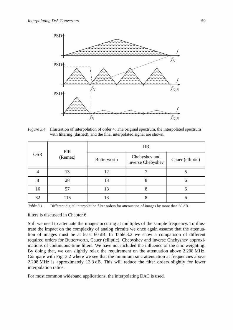
Interpolating D/A Converters 59
illus-tenua-rent
proxi-ting.Hz.
aboveer
m
filters is discussed in Chapter 6.
Still we need to attenuate the images occuring at multiples of the sample frequency. Totrate the impact on the complexity of analog circuits we once again assume that the attion of images must be at least 60 dB. In Table 3.2 we show a comparison of differequired orders for Butterworth, Cauer (elliptic), Chebyshev and inverse Chebyshev apmations of continuous-time filters. We have not included the influence of the sinc weighBy doing that, we can slightly relax the requirement on the attenuation above 2.208 MCompare with Fig. 3.2 where we see that the minimum sinc attenuation at frequencies2.208 MHz is approximately 13.3 dB. This will reduce the filter orders slightly for lowinterpolation ratios.
For most common wideband applications, the interpolating DAC is used.
Figure 3.4 Illustration of interpolation of order 4. The original spectrum, the interpolated spectruwith filtering (dashed), and the final interpolated signal are shown.
OSRFIR
(Remez)
IIR
ButterworthChebyshev and
inverse ChebyshevCauer (elliptic)
4 13 12 7 5
8 28 13 8 6
16 57 13 8 6
32 115 13 8 6
Table 3.1. Different digital interpolation filter orders for attenuation of images by more than 60 dB.
fN
f
fN
fN
fO,N
fO,N
f
f
PSD
PSD
PSD
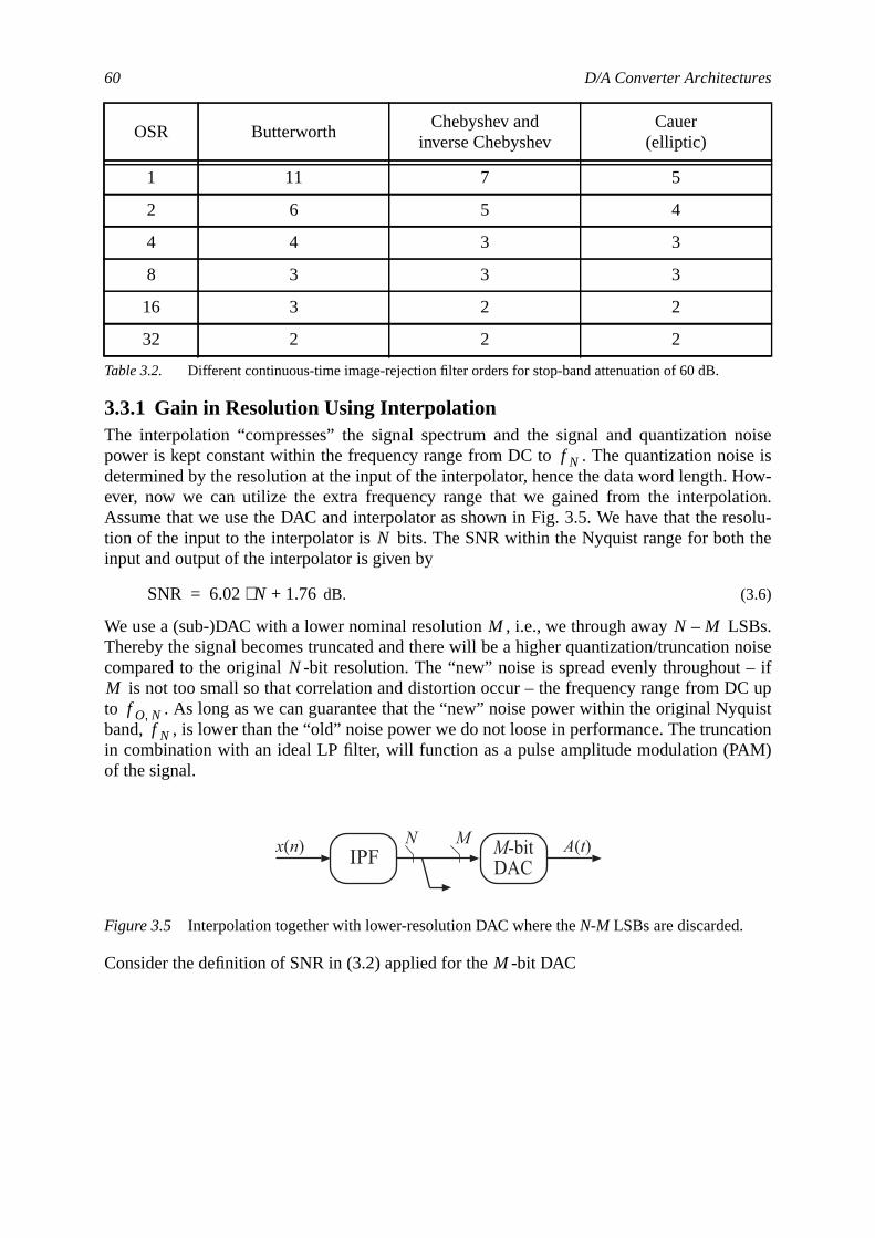
60 D/A Converter Architectures
noisese isHow-tion.
esolu-the
Bs.noise– if
C upuist
ationM)
3.3.1 Gain in Resolution Using InterpolationThe interpolation “compresses” the signal spectrum and the signal and quantizationpower is kept constant within the frequency range from DC to . The quantization noidetermined by the resolution at the input of the interpolator, hence the data word length.ever, now we can utilize the extra frequency range that we gained from the interpolaAssume that we use the DAC and interpolator as shown in Fig. 3.5. We have that the rtion of the input to the interpolator is bits. The SNR within the Nyquist range for bothinput and output of the interpolator is given by
dB. (3.6)
We use a (sub-)DAC with a lower nominal resolution , i.e., we through away LSThereby the signal becomes truncated and there will be a higher quantization/truncationcompared to the original -bit resolution. The “new” noise is spread evenly throughout
is not too small so that correlation and distortion occur – the frequency range from Dto . As long as we can guarantee that the “new” noise power within the original Nyqband, , is lower than the “old” noise power we do not loose in performance. The truncin combination with an ideal LP filter, will function as a pulse amplitude modulation (PAof the signal.
Consider the definition of SNR in (3.2) applied for the -bit DAC
OSR ButterworthChebyshev and
inverse ChebyshevCauer
(elliptic)
1 11 7 5
2 6 5 4
4 4 3 3
8 3 3 3
16 3 2 2
32 2 2 2
Table 3.2. Different continuous-time image-rejection filter orders for stop-band attenuation of 60 dB.
Figure 3.5 Interpolation together with lower-resolution DAC where theN-M LSBs are discarded.
f N
N
SNR 6.02 N⋅ 1.76+=
M N M–
NM
f O N,f N
IPF M-bitDAC
N Mx(n) A(t)
M
Interpolating D/A Converters 61
hownhis
ared
its ismpare
ersbandfre-
reachfiltersn ofca-
digitalever, area.
dB, (3.7)
where is the noise power spectral density. If we assume an ideal LP filter (as sin Fig. 3.4 (b)) with cut-off frequency at , we only have to consider the SNR within tfrequency range, which is expressed by the first term in (3.7). Hence, we have
dB. (3.8)
From (3.8) we can draw the intuitive conclusion that the narrower signal bandwidth compto the update frequency (higher OSR), the higher SNR. (3.8) can be written as
dB. (3.9)
From (3.8) and (3.9) we find that for each doubling of the OSR, the effective number of bincreased by half a bit. To guarantee that we do not loose in resolution we need to co(3.9) with (3.6) and we have
(3.10)
or
. (3.11)
For example, if and , we can use a 12-bit (11.5-bit) DAC. Anothadvantage of using a smaller bandwidth is the lower sinc attenuation of signal at the pasedge (see Fig. 3.2 for ). The attenuation of the signal at the original Nyquistquency is given by
. (3.12)
If, for example, , we have an approximate attenuation of only 0.1 dB.
It becomes obvious from the previous discussion that a high OSR is a good approach tohigh performance. The advantages are that we may relax the analog image-rejectionsignificantly, we may use a DAC with a lower nominal resolution, and the sinc attenuatiothe signal is lower. Notice, that the linearity of the DAC must still meet the -bit specifition. The disadvantages with oversampling are that there is an increased complexity ofcircuits and the clock frequency, chip area, and power consumption is increased. Howsince the analog filter has a lower order, it will consume less power and occupy less chip
SNRM 10Ps
SqM( ) f( ) f O N,⋅
-----------------------------------log10⋅ 10Ps
SqM( ) f( ) f N⋅
------------------------------f N
f O N,------------⋅
log10⋅= = =
10Ps
SqM( ) f( ) f N⋅
------------------------------log10⋅ 10f N
f O N,------------log10⋅–= =
10Ps
SqM( ) f( ) f N⋅
------------------------------log10⋅ 10 OSRlog10⋅–=
SqM( ) f( )
f N
SNR SNRM 10 OSRlog10⋅+=
SNR 6.02 M⋅ 1.76 10 OSRlog10⋅+ +=
6.02 M⋅ 1.76 10 OSRlog10⋅+ + 6.02 N⋅ 1.76+>
M NOSRlog10
4log10
-----------------------– N 1.66 OSRlog10⋅–≈>
N 14= OSR 32=
f sig f u⁄ 0.5<
Asinc f N( ) 10–π f N
f O u,-----------sinc
2log10⋅ 20–
π 2⁄OSR-----------sinclog10⋅= =
OSR 16=
N
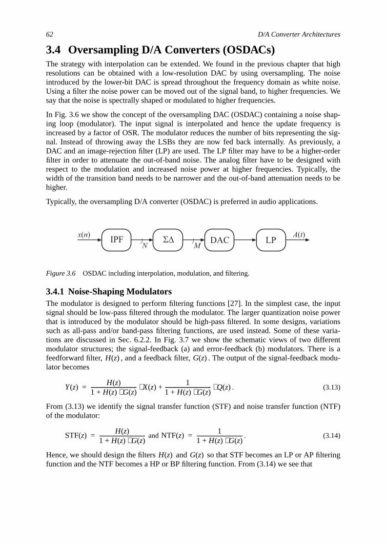
62 D/A Converter Architectures
t highoiseoise.s. We
hap-cy ise sig-
ly, aorder
withy, thes to be
inputower
ationsvaria-
erente is aodu-
TF)
ering
3.4 Oversampling D/A Converters (OSDACs)The strategy with interpolation can be extended. We found in the previous chapter tharesolutions can be obtained with a low-resolution DAC by using oversampling. The nintroduced by the lower-bit DAC is spread throughout the frequency domain as white nUsing a filter the noise power can be moved out of the signal band, to higher frequenciesay that the noise is spectrally shaped or modulated to higher frequencies.
In Fig. 3.6 we show the concept of the oversampling DAC (OSDAC) containing a noise sing loop (modulator). The input signal is interpolated and hence the update frequenincreased by a factor of OSR. The modulator reduces the number of bits representing thnal. Instead of throwing away the LSBs they are now fed back internally. As previousDAC and an image-rejection filter (LP) are used. The LP filter may have to be a higher-filter in order to attenuate the out-of-band noise. The analog filter have to be designedrespect to the modulation and increased noise power at higher frequencies. Typicallwidth of the transition band needs to be narrower and the out-of-band attenuation needhigher.
Typically, the oversampling D/A converter (OSDAC) is preferred in audio applications.
3.4.1 Noise-Shaping ModulatorsThe modulator is designed to perform filtering functions [27]. In the simplest case, thesignal should be low-pass filtered through the modulator. The larger quantization noise pthat is introduced by the modulator should be high-pass filtered. In some designs, varisuch as all-pass and/or band-pass filtering functions, are used instead. Some of thesetions are discussed in Sec. 6.2.2. In Fig. 3.7 we show the schematic views of two diffmodulator structures; the signal-feedback (a) and error-feedback (b) modulators. Therfeedforward filter, , and a feedback filter, . The output of the signal-feedback mlator becomes
. (3.13)
From (3.13) we identify the signal transfer function (STF) and noise transfer function (Nof the modulator:
and . (3.14)
Hence, we should design the filters and so that STF becomes an LP or AP filtfunction and the NTF becomes a HP or BP filtering function. From (3.14) we see that
Figure 3.6 OSDAC including interpolation, modulation, and filtering.
DAC LPSDIPFx(n) A(t)N M
H z( ) G z( )
Y z( )H z( )
1 H z( ) G z( )⋅+----------------------------------- X z( )⋅ 1
1 H z( ) G z( )⋅+----------------------------------- Q z( )⋅+=
STF z( ) H z( )1 H z( ) G z( )⋅+-----------------------------------= NTF z( ) 1
1 H z( ) G z( )⋅+-----------------------------------=
H z( ) G z( )
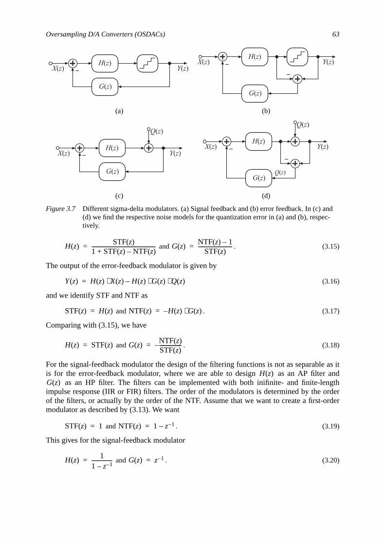
Oversampling D/A Converters (OSDACs) 63
e as itr andgthorderrder
andec-
and . (3.15)
The output of the error-feedback modulator is given by
(3.16)
and we identify STF and NTF as
and . (3.17)
Comparing with (3.15), we have
and . (3.18)
For the signal-feedback modulator the design of the filtering functions is not as separablis for the error-feedback modulator, where we are able to design as an AP filte
as an HP filter. The filters can be implemented with both inifinite- and finite-lenimpulse response (IIR or FIR) filters. The order of the modulators is determined by theof the filters, or actually by the order of the NTF. Assume that we want to create a first-omodulator as described by (3.13). We want
and . (3.19)
This gives for the signal-feedback modulator
and . (3.20)
(a) (b)
(c) (d)
Figure 3.7 Different sigma-delta modulators. (a) Signal feedback and (b) error feedback. In (c) (d) we find the respective noise models for the quantization error in (a) and (b), resptively.
H(z)
G(z)
Y(z)X(z)
H(z)
G(z)
Y(z)X(z)
H(z)
G(z)
Y(z)
Q(z)
X(z)
H(z)
G(z)
Y(z)
Q(z)
X(z)
Q(z)
H z( ) STF z( )1 STFz( ) NTF z( )–+-------------------------------------------------= G z( ) NTF z( ) 1–
STF z( )--------------------------=
Y z( ) H z( ) X z( )⋅ H z( ) G z( ) Q z( )⋅ ⋅–=
STF z( ) H z( )= NTF z( ) H z( ) G z( )⋅–=
H z( ) STF z( )= G z( ) NTF z( )STF z( )-----------------–=
H z( )G z( )
STF z( ) 1= NTF z( ) 1 z 1––=
H z( ) 11 z 1––----------------= G z( ) z 1–=
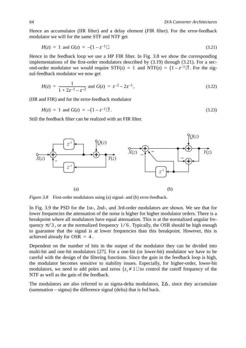
64 D/A Converter Architectures
back
dingsec-
ig-
at forre is aar fre-oughhis is
intobeigh,
er-bitf the
ulate
Hence an accumulator (IIR filter) and a delay element (FIR filter). For the error-feedmodulator we will for the same STF and NTF get
and . (3.21)
Hence in the feedback loop we use a HP FIR filter. In Fig. 3.8 we show the corresponimplementations of the first-order modulators described by (3.19) through (3.21). For aond-order modulator we would require and . For the snal-feedback modulator we now get
and , (3.22)
(IIR and FIR) and for the error-feedback modulator
and . (3.23)
Still the feedback filter can be realized with an FIR filter.
In Fig. 3.9 the PSD for the 1st-, 2nd-, and 3rd-order modulators are shown. We see thlower frequencies the attenuation of the noise is higher for higher modulator orders. Thebreakpoint where all modulators have equal attenuation. This is at the normalized angulquency , or at the normalized frequency . Typically, the OSR should be high ento guarantee that the signal is at lower frequencies than this breakpoint. However, tachieved already for .
Dependent on the number of bits in the output of the modulator they can be dividedmulti-bit and one-bit modulators [27]. For a one-bit (or lower-bit) modulator we have tocareful with the design of the filtering functions. Since the gain in the feedback loop is hthe modulator becomes sensitive to stability issues. Especially, for higher-order, lowmodulators, we need to add poles and zeros to control the cutoff frequency oNTF as well as the gain of the feedback.
The modulators are also referred to as sigma-delta modulators, , since they accum(summation – sigma) the difference signal (delta) that is fed back.
(a) (b)
Figure 3.8 First-order modulators using (a) signal- and (b) error-feedback.
H z( ) 1= G z( ) 1 z 1––( )–=
STF z( ) 1= NTF z( ) 1 z 1––( )2=
H z( ) 11 2z 1– z 2––+---------------------------------= G z( ) z 2– 2z 1––=
H z( ) 1= G z( ) 1 z 1––( )2–=
z-1
z-1
Y(z)
Q(z)
X(z)
z-1
Y(z)
Q(z)
X(z)
π 3⁄ 1 6⁄
OSR 4=
zi 1≠( )
Σ∆
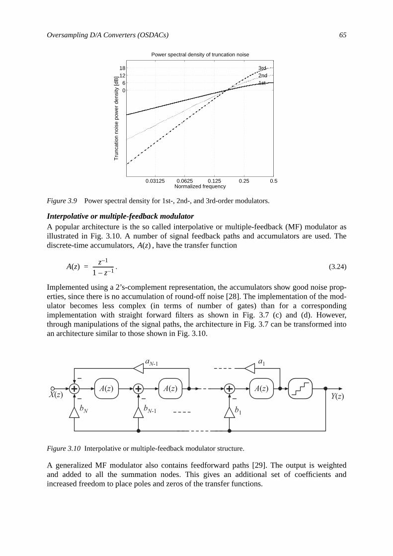
Oversampling D/A Converters (OSDACs) 65
r as. The
prop-mod-ndingver,d into
htedand
Interpolative or multiple-feedback modulatorA popular architecture is the so called interpolative or multiple-feedback (MF) modulatoillustrated in Fig. 3.10. A number of signal feedback paths and accumulators are useddiscrete-time accumulators, , have the transfer function
. (3.24)
Implemented using a 2’s-complement representation, the accumulators show good noiseerties, since there is no accumulation of round-off noise [28]. The implementation of theulator becomes less complex (in terms of number of gates) than for a correspoimplementation with straight forward filters as shown in Fig. 3.7 (c) and (d). Howethrough manipulations of the signal paths, the architecture in Fig. 3.7 can be transformean architecture similar to those shown in Fig. 3.10.
A generalized MF modulator also contains feedforward paths [29]. The output is weigand added to all the summation nodes. This gives an additional set of coefficientsincreased freedom to place poles and zeros of the transfer functions.
Figure 3.9 Power spectral density for 1st-, 2nd-, and 3rd-order modulators.
Figure 3.10 Interpolative or multiple-feedback modulator structure.
0.03125 0.0625 0.125 0.25 0.5
06
1218
Normalized frequency
Tru
ncat
ion
nois
e po
wer
den
sity
[dB
]
Power spectral density of truncation noise
1st2nd3rd
A z( )
A z( ) z 1–
1 z 1––----------------=
b1bN-1bN
aN-1 a1
Y(z)X(z)A(z) A(z) A(z)
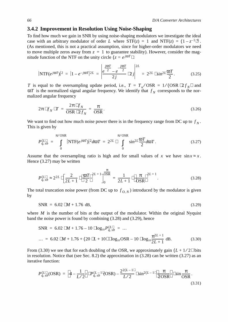
66 D/A Converter Architectures
ideal.
needag-
ndnor-
.
.
iven
uist
bitsas an
3.4.2 Improvement in Resolution Using Noise-ShapingTo find how much we gain in SNR by using noise-shaping modulators we investigate thecase with an arbitrary modulator of order where and(As mentioned, this is not a practical assumption, since for higher-order modulators weto move multiple zeros away from to guarantee stability). However, consider the mnitude function of the NTF on the unity circle :
. (3.25)
is equal to the oversampling update period, i.e., ais the normalized signal angular frequency. We identify that corresponds to the
malized angular frequency
. (3.26)
We want to find out how much noise power there is in the frequency range from DC up toThis is given by
. (3.27)
Assume that the oversampling ratio is high and for small values of we haveHence (3.27) may be written
. (3.28)
The total truncation noise power (from DC up to ) introduced by the modulator is gby
dB, (3.29)
where is the number of bits at the output of the modulator. Within the original Nyqband the noise power is found by combining (3.28) and (3.29), hence
dB. (3.30)
From (3.30) we see that for each doubling of the OSR, we approximately gainin resolution. Notice that (see Sec. 8.2) the approximation in (3.28) can be written (3.27)iterative function:
.
(3.31)
L STF z( ) 1= NTF z( ) 1 z 1––( )L=
z 1=z ejωT=( )
NTF ejωT( ) 2 1 e jωT–– 2L ejωT2
-----------e
jωT2
-----------––2 j
------------------------------- 2 j⋅
2L
22L ωT2
--------sin2L⋅= = =
T T Tu OSR⁄ 1 OSR 2f N⋅( )⁄= =ωT f N
2π f N T⋅ ⋅2π f N⋅
OSR 2f N⋅-------------------------- π
OSR-----------= =
f N
Pq sb,L( ) NTF ejωT( ) 2 ωTd
0
π OSR⁄
∫ 22L ωT2
--------sin2L ωTd
0
π OSR⁄
∫⋅= =
x xsin x≈
Pq sb,L( ) 22L 2
2L 1+---------------- ωT
2--------
2L 1+⋅
0
πOSR-----------
⋅≈ 12L 1+---------------- π
OSR-----------
2L 1+⋅=
f O N,
SNR 6.02 M⋅ 1.76+=
M
SNR 6.02 M⋅ 1.76 10 Pq sb,L( )log10⋅–+ …= =
… 6.02 M⋅ 1.76 20 L⋅ 10+( ) OSRlog10⋅ 10π2L 1+
2L 1+----------------log10⋅–+ +=
L 1 2⁄+( )
Pq sb,L( ) OSR( ) 4 1
L 2⁄----------–
Pq sb,L 1–( ) OSR( )⋅ 22 L 1–( )
L 2⁄------------------ π
2OSR---------------
sin2 L 1–( ) πOSR-----------sin⋅ ⋅–=
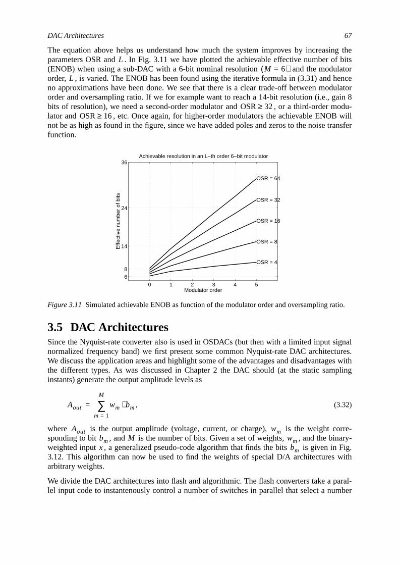
DAC Architectures 67
ing thef bitstorencedulatorain 8odu-will
transfer
ignaltures.es withpling
rre-ary-Fig.with
aral-mber
tio.
The equation above helps us understand how much the system improves by increasparameters OSR and . In Fig. 3.11 we have plotted the achievable effective number o(ENOB) when using a sub-DAC with a 6-bit nominal resolution and the modulaorder, , is varied. The ENOB has been found using the iterative formula in (3.31) and hno approximations have been done. We see that there is a clear trade-off between moorder and oversampling ratio. If we for example want to reach a 14-bit resolution (i.e., gbits of resolution), we need a second-order modulator and , or a third-order mlator and , etc. Once again, for higher-order modulators the achievable ENOBnot be as high as found in the figure, since we have added poles and zeros to the noisefunction.
3.5 DAC ArchitecturesSince the Nyquist-rate converter also is used in OSDACs (but then with a limited input snormalized frequency band) we first present some common Nyquist-rate DAC architecWe discuss the application areas and highlight some of the advantages and disadvantagthe different types. As was discussed in Chapter 2 the DAC should (at the static saminstants) generate the output amplitude levels as
, (3.32)
where is the output amplitude (voltage, current, or charge), is the weight cosponding to bit , and is the number of bits. Given a set of weights, , and the binweighted input , a generalized pseudo-code algorithm that finds the bits is given in3.12. This algorithm can now be used to find the weights of special D/A architecturesarbitrary weights.
We divide the DAC architectures into flash and algorithmic. The flash converters take a plel input code to instantenously control a number of switches in parallel that select a nu
Figure 3.11 Simulated achievable ENOB as function of the modulator order and oversampling ra
LM 6=( )
L
OSR 32≥OSR 16≥
0 1 2 3 4 5
68
14
24
36
OSR = 4
OSR = 8
OSR = 16
OSR = 32
OSR = 64
Modulator order
Effe
ctiv
e nu
mbe
r of
bits
Achievable resolution in an L−th order 6−bit modulator
Aout wm bm⋅m 1=
M
∑=
Aout wmbm M wmx bm
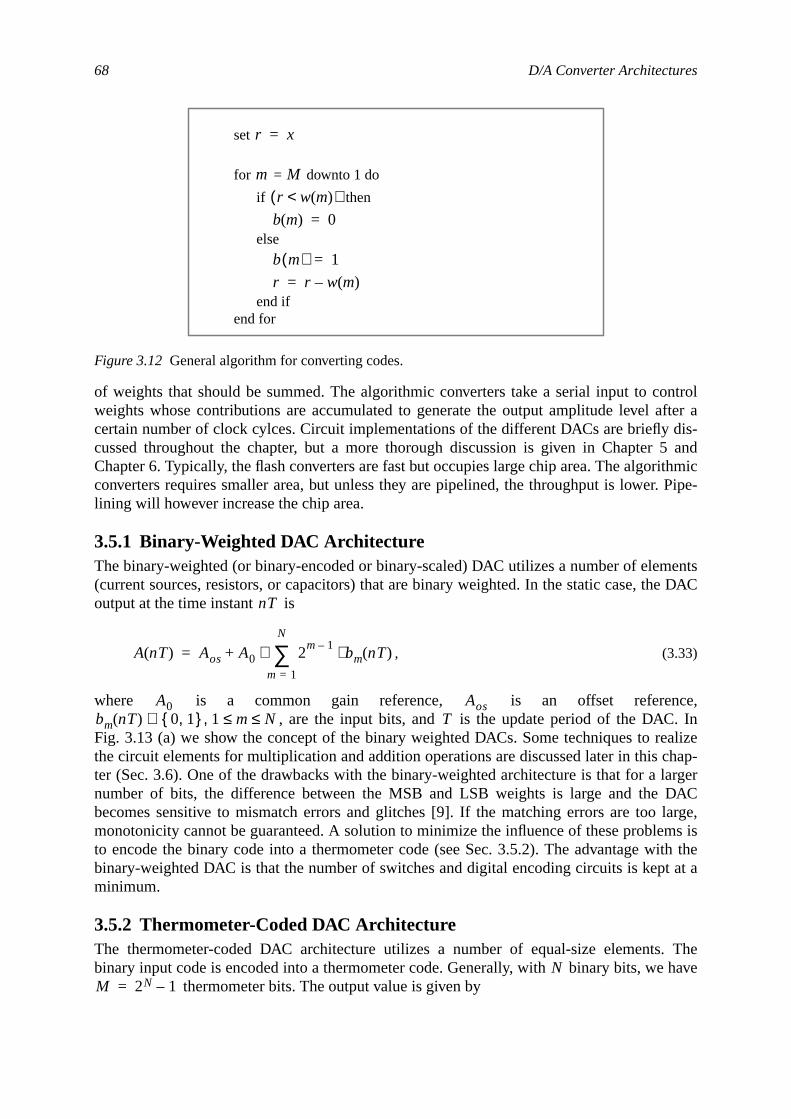
68 D/A Converter Architectures
ntrolfter adis-5 andithmic. Pipe-
entse DAC
ce,In
ealizechap-argerDAClarge,ms isith theat a
. Thehave
of weights that should be summed. The algorithmic converters take a serial input to coweights whose contributions are accumulated to generate the output amplitude level acertain number of clock cylces. Circuit implementations of the different DACs are brieflycussed throughout the chapter, but a more thorough discussion is given in ChapterChapter 6. Typically, the flash converters are fast but occupies large chip area. The algorconverters requires smaller area, but unless they are pipelined, the throughput is lowerlining will however increase the chip area.
3.5.1 Binary-Weighted DAC ArchitectureThe binary-weighted (or binary-encoded or binary-scaled) DAC utilizes a number of elem(current sources, resistors, or capacitors) that are binary weighted. In the static case, thoutput at the time instant is
, (3.33)
where is a common gain reference, is an offset referen, are the input bits, and is the update period of the DAC.
Fig. 3.13 (a) we show the concept of the binary weighted DACs. Some techniques to rthe circuit elements for multiplication and addition operations are discussed later in thister (Sec. 3.6). One of the drawbacks with the binary-weighted architecture is that for a lnumber of bits, the difference between the MSB and LSB weights is large and thebecomes sensitive to mismatch errors and glitches [9]. If the matching errors are toomonotonicity cannot be guaranteed. A solution to minimize the influence of these probleto encode the binary code into a thermometer code (see Sec. 3.5.2). The advantage wbinary-weighted DAC is that the number of switches and digital encoding circuits is keptminimum.
3.5.2 Thermometer-Coded DAC ArchitectureThe thermometer-coded DAC architecture utilizes a number of equal-size elementsbinary input code is encoded into a thermometer code. Generally, with binary bits, we
thermometer bits. The output value is given by
Figure 3.12 General algorithm for converting codes.
set
for = downto 1 do
if then
else
end ifend for
r x=
m M
r w m( )<( )b m( ) 0=
b m( ) 1=
r r w m( )–=
nT
A nT( ) Aos A0 2m 1–
bm nT( )⋅m 1=
N
∑⋅+=
A0 Aosbm nT( ) 0 1, ∈ 1 m N≤ ≤, T
NM 2N 1–=
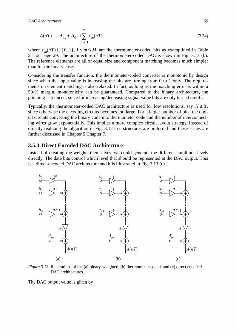
DAC Architectures 69
ble3 (b).simpler
esignuire-thin a, the
/off.
,digi-
nect-d ofes are
levelsThis
d
, (3.34)
where are the thermometer-coded bits as examplified in Ta2.1 on page 29. The architecture of the thermometer-coded DAC is shown in Fig. 3.1The reference elements are all of equal size and component matching becomes muchthan for the binary case.
Considering the transfer function, the thermometer-coded converter is monotonic by dsince when the input value is increasing the bits are turning from 0 to 1 only. The reqments on element matching is also relaxed. In fact, as long as the matching error is wi50-% margin, monotonicity can be guaranteed. Compared to the binary architectureglitching is reduced, since for increasing/decreasing signal value bits are only turned on
Typically, the thermometer-coded DAC architecture is used for low resolutions, saysince otherwise the encoding circuits becomes too large. For a larger number of bits, thetal circuits converting the binary code into thermometer code and the number of interconing wires grow exponentially. This implies a more complex circuit layout strategy. Insteadirectly realizing the algorithm in Fig. 3.12 tree structures are preferred and these issufurther discussed in Chapter 5 Chapter 7.
3.5.3 Direct Encoded DAC ArchitectureInstead of creating the weights themselves, we could generate the different amplitudedirectly. The data bits control which level that should be represented at the DAC output.is a direct-encoded DAC architecture and it is illustrated in Fig. 3.13 (c).
The DAC output value is given by
(a) (b) (c)
Figure 3.13 Illustrations of the (a) binary-weighted, (b) thermometer-coded, and (c) direct encodeDAC architectures.
A nT( ) Aos A0 cm nT( )m 1=
M
∑⋅+=
cm nT( ) 0 1, ∈ 1 m M≤ ≤,
N 8≤
Aos
b1
b2
bN
A0
20
21
2N-1
A(nT)
Aos
c1
c2
cM
A0
1
1
1
A(nT)
Aos
d1
d2
dM
A0
1
2
2N-1
A(nT)
70 D/A Converter Architectures
inther thetingnts. Inrough
switchs theltage
guar-
ed lin-the
or the
v-
dvan-es as7.
disad-erfor-
rententedd thefind
cuits,
, (3.35)
where are bits given by a “walking-one” code as examplifiedTable 2.1 on page 29. For an -bit DAC we need . Encoders convertingbinary code into the “walking-one” code have the same complexity as the the ones fothermometer-coded DAC. In fact, the two DAC architectures are basically similar. Rouand occupied chip area become large and complex due to the large number of componeterms of propagation time, the encoding circuits can be pipelined and the propagation ththe encoder becomes a minor problem.
The drawback is that we need a large number of elements, since one element and oneis needed for each conversion level. A typical implementation using this architecture iresistor-string DAC (Sec. 3.6.4) where resistors are used to divide a reference vointo the different conversion voltage levels. With such an approach, monotonicity can beanteed.
3.5.4 Linear-Coded DAC ArchitectureBetween the two extremes; binary-weighted and thermometer-coded, we put the proposear-coded DAC [32, 33, 34, 35]. The architecture is similar to that of Fig. 3.13 whereweights are linearly increasing. The output level is given by the same expression as fdirect encoded DAC (3.35) as
, (3.36)
where . However, unlike the direct encoded DAC we allow seeral bits to be 1 at the same time. The number of bits of the linear code is given by
. (3.37)
The binary-to-linear encoder becomes complex. The linear DAC shows to have some atages in terms of linearity and glitch performance over the regular converter architecturdescribed above. The properties of linear-coded DACs are further discussed in Chapter
3.5.5 Hybrid DAC ArchitecturesAs has been briefly issued above, the DAC architectures have different advantages andvantages. Therefore the combination of different techniques can be used to improve pmance. This is illustrated by the hybrid converter in Fig. 3.14 where the diffesubconverters, , can be of various types. One popular hybrid is the so called segmarchitecture [9, 30]. The more significant bits are encoded into a thermometer code anless significant bits are binary weighted. One of the key issues in this kind of hybrid is tothe optimum number of bits to encode into thermometer code. The increase of digital cirnoise, chip area, vs. performance, etc., thereby have to be taken into account.
A nT( ) Aos A0 m dm nT( )⋅m 1=
M
∑⋅+=
dm nT( ) 0 1, ∈ 1 m M≤ ≤,N M 2N 1–=
2N 1–
A nT( ) Aos A0 m em nT( )⋅m 1=
M
∑⋅+=
em nT( ) 0 1, ∈ 1 m M≤ ≤,
M 2N 3+ 7– 1+2
------------------------------------=
DACi
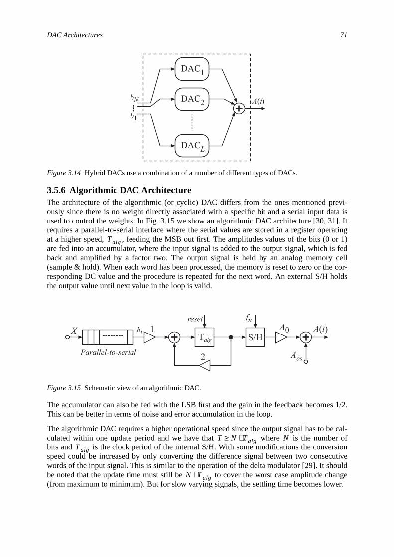
DAC Architectures 71
evi-ata is1]. Itrating
or 1)is fedcell
he cor-holds
s 1/2.
e cal-er ofsioncutiveouldangeer.
3.5.6 Algorithmic DAC ArchitectureThe architecture of the algorithmic (or cyclic) DAC differs from the ones mentioned prously since there is no weight directly associated with a specific bit and a serial input dused to control the weights. In Fig. 3.15 we show an algorithmic DAC architecture [30, 3requires a parallel-to-serial interface where the serial values are stored in a register opeat a higher speed, , feeding the MSB out first. The amplitudes values of the bits (0are fed into an accumulator, where the input signal is added to the output signal, whichback and amplified by a factor two. The output signal is held by an analog memory(sample & hold). When each word has been processed, the memory is reset to zero or tresponding DC value and the procedure is repeated for the next word. An external S/Hthe output value until next value in the loop is valid.
The accumulator can also be fed with the LSB first and the gain in the feedback becomeThis can be better in terms of noise and error accumulation in the loop.
The algorithmic DAC requires a higher operational speed since the output signal has to bculated within one update period and we have that where is the numbbits and is the clock period of the internal S/H. With some modifications the converspeed could be increased by only converting the difference signal between two consewords of the input signal. This is similar to the operation of the delta modulator [29]. It shbe noted that the update time must still be to cover the worst case amplitude ch(from maximum to minimum). But for slow varying signals, the settling time becomes low
Figure 3.14 Hybrid DACs use a combination of a number of different types of DACs.
Figure 3.15 Schematic view of an algorithmic DAC.
DAC1
DAC2
DACL
bN
b1
A(t)
Talg
Aos
biA0
2
S/H1X
fuA(t)
Parallel-to-serial
reset
Talg
T N Talg⋅≥ NTalg
N Talg⋅
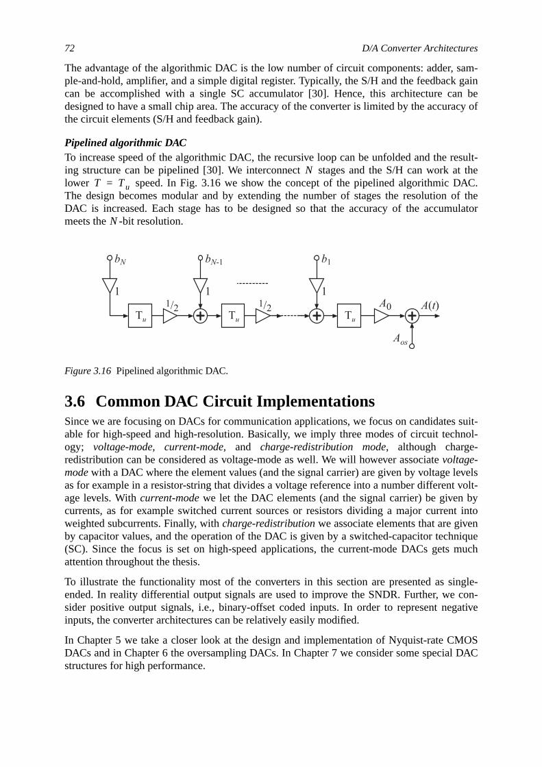
72 D/A Converter Architectures
sam-gain
an beacy of
esult-at theAC.of theulator
suit-nol-
evelst volt-byt inton
niquemuch
ingle-con-ative
MOSDAC
The advantage of the algorithmic DAC is the low number of circuit components: adder,ple-and-hold, amplifier, and a simple digital register. Typically, the S/H and the feedbackcan be accomplished with a single SC accumulator [30]. Hence, this architecture cdesigned to have a small chip area. The accuracy of the converter is limited by the accurthe circuit elements (S/H and feedback gain).
Pipelined algorithmic DACTo increase speed of the algorithmic DAC, the recursive loop can be unfolded and the ring structure can be pipelined [30]. We interconnect stages and the S/H can worklower speed. In Fig. 3.16 we show the concept of the pipelined algorithmic DThe design becomes modular and by extending the number of stages the resolutionDAC is increased. Each stage has to be designed so that the accuracy of the accummeets the -bit resolution.
3.6 Common DAC Circuit ImplementationsSince we are focusing on DACs for communication applications, we focus on candidatesable for high-speed and high-resolution. Basically, we imply three modes of circuit techogy; voltage-mode, current-mode,and charge-redistribution mode, although charge-redistribution can be considered as voltage-mode as well. We will however associatevoltage-modewith a DAC where the element values (and the signal carrier) are given by voltage las for example in a resistor-string that divides a voltage reference into a number differenage levels. Withcurrent-modewe let the DAC elements (and the signal carrier) be givencurrents, as for example switched current sources or resistors dividing a major currenweighted subcurrents. Finally, withcharge-redistributionwe associate elements that are giveby capacitor values, and the operation of the DAC is given by a switched-capacitor tech(SC). Since the focus is set on high-speed applications, the current-mode DACs getsattention throughout the thesis.
To illustrate the functionality most of the converters in this section are presented as sended. In reality differential output signals are used to improve the SNDR. Further, wesider positive output signals, i.e., binary-offset coded inputs. In order to represent neginputs, the converter architectures can be relatively easily modified.
In Chapter 5 we take a closer look at the design and implementation of Nyquist-rate CDACs and in Chapter 6 the oversampling DACs. In Chapter 7 we consider some specialstructures for high performance.
Figure 3.16 Pipelined algorithmic DAC.
NT Tu=
N
1/21
Aos
A0 A(t)
bN
1/21 1
bN-1 b1
Tu Tu Tu
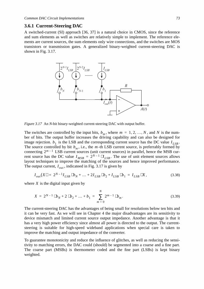
Common DAC Circuit Implementations 73
encee ele-e MOSC is
um-d for
.d by
cur-lowsance.
ts andity tothat itrrent-en to
sensi-part.
inary
3.6.1 Current-Steering DACA switched-current (SI) approach [36, 37] is a natural choice in CMOS, since the referand sum elements as well as switches are relatively simple to implement. The referencments are current sources, the sum elements only wire connections, and the switches artransistors or transmission gates. A generalized binary-weighted current-steering DAshown in Fig. 3.17.
The switches are controlled by the input bits, , where , and is the nber of bits. The output buffer increases the driving capability and can also be designeimage rejection. is the LSB and the corresponding current source has the DC valueThe source controlled by bit , i.e., the -th LSB current source, is preferrably formeconnecting LSB current sources (unit current sources) in parallel, hence the MSBrent source has the DC value . The use of unit element sources allayout techniques to improve the matching of the sources and hence improved performThe output current, , indicateed in Fig. 3.17 is given by
, (3.38)
where is the digital input given by
. (3.39)
The current-steering DAC has the advantages of being small for resolutions below ten biit can be very fast. As we will see in Chapter 4 the major disadvantages are its sensitivdevice mismatch and limited current source output impedance. Another advantage ishas a very high power efficiency since almost all power is directed to the output. The custeering is suitable for high-speed wideband applications when special care is takimprove the matching and output impedance of the converter.
To guarantee monotonicity and reduce the influence of glitches, as well as reducing thetivity to matching errors, the DAC could (should) be segmented into a coarse and a fineThe coarse part (MSBs) is thermometer coded and the fine part (LSBs) is kept bweighted.
Figure 3.17 An N-bit binary-weighted current-steering DAC with output buffer.
R
A(t)
ILSB2N-1ILSB 2N-2ILSB
bN bN-1 b1
Iout(t)
bm m 1 2 … N, , ,= N
b1 I LSBbm m
2m 1–
I MSB 2N 1– I LSB⋅=
I out
I out X( ) 2N 1– I LSB bN⋅ … 2I LSB b2⋅ I LSB b1⋅+ + + I LSB X⋅= =
X
X 2N 1– bN⋅ 2 b2⋅ … b1+ + + 2m 1– bm⋅m 0=
N
∑= =
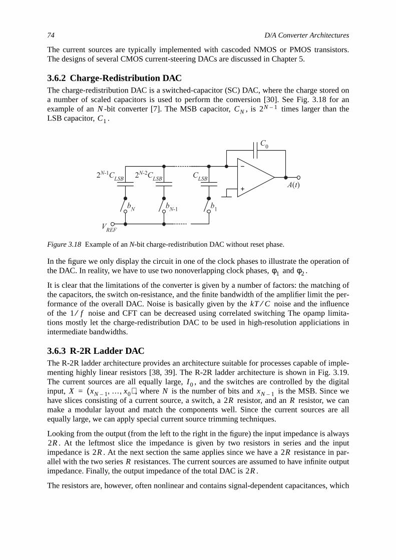
74 D/A Converter Architectures
stors.
ed onfor anthe
n of
g ofper-nceimita-s in
imple-.19.igital
wee can
are all
aysinputin par-output
, which
The current sources are typically implemented with cascoded NMOS or PMOS transiThe designs of several CMOS current-steering DACs are discussed in Chapter 5.
3.6.2 Charge-Redistribution DACThe charge-redistribution DAC is a switched-capacitor (SC) DAC, where the charge stora number of scaled capacitors is used to perform the conversion [30]. See Fig. 3.18example of an -bit converter [7]. The MSB capacitor, , is times larger thanLSB capacitor, .
In the figure we only display the circuit in one of the clock phases to illustrate the operatiothe DAC. In reality, we have to use two nonoverlapping clock phases, and .
It is clear that the limitations of the converter is given by a number of factors: the matchinthe capacitors, the switch on-resistance, and the finite bandwidth of the amplifier limit theformance of the overall DAC. Noise is basically given by the noise and the influeof the noise and CFT can be decreased using correlated switching The opamp ltions mostly let the charge-redistribution DAC to be used in high-resolution appliciationintermediate bandwidths.
3.6.3 R-2R Ladder DACThe R-2R ladder architecture provides an architecture suitable for processes capable ofmenting highly linear resistors [38, 39]. The R-2R ladder architecture is shown in Fig. 3The current sources are all equally large, , and the switches are controlled by the dinput, , where is the number of bits and is the MSB. Sincehave slices consisting of a current source, a switch, a resistor, and an resistor, wmake a modular layout and match the components well. Since the current sourcesequally large, we can apply special current source trimming techniques.
Looking from the output (from the left to the right in the figure) the input impedance is alw. At the leftmost slice the impedance is given by two resistors in series and the
impedance is . At the next section the same applies since we have a resistanceallel with the two series resistances. The current sources are assumed to have infiniteimpedance. Finally, the output impedance of the total DAC is .
The resistors are, however, often nonlinear and contains signal-dependent capacitances
Figure 3.18 Example of anN-bit charge-redistribution DAC without reset phase.
N CN 2N 1–
C1
A(t)CLSB2N-1CLSB 2N-2CLSB
bN bN-1 b1
C0
VREF
φ1 φ2
kT C⁄1 f⁄
I 0X xN 1– … x0, ,( )= N xN 1–
2R R
2R2R 2R
R2R
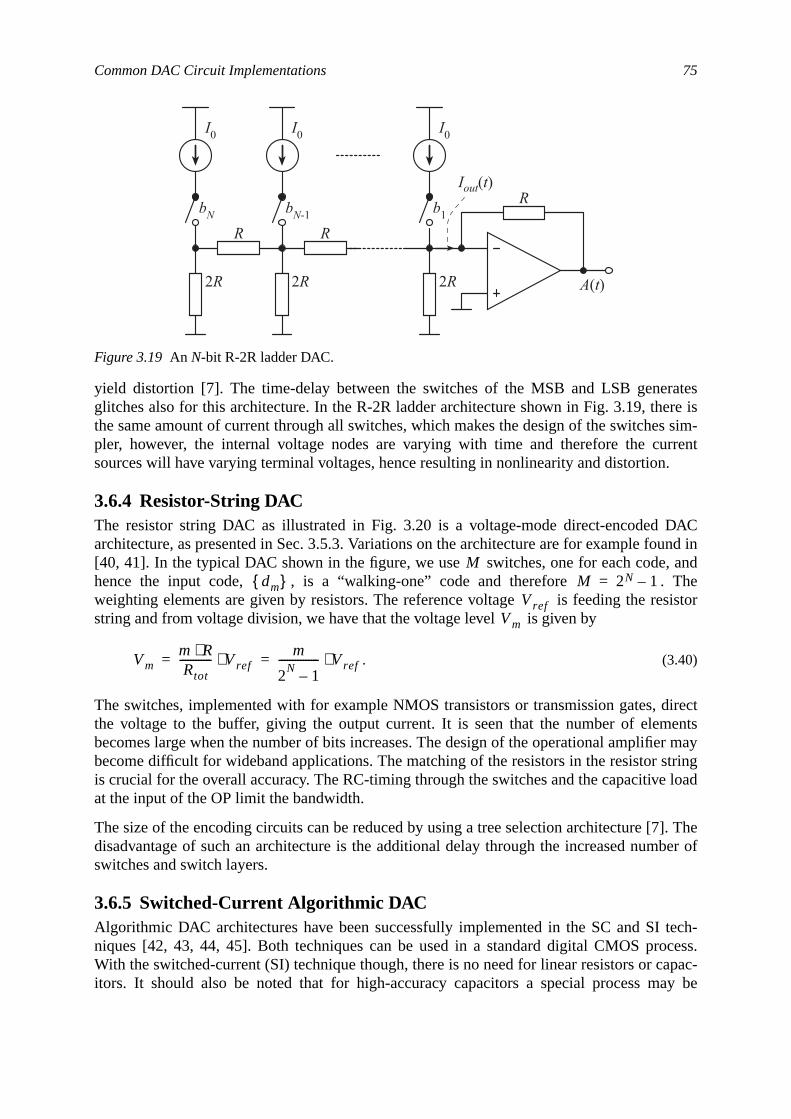
Common DAC Circuit Implementations 75
ratesere iss sim-rrent.
DACund in
, andhesistor
directentsr maytringload
]. Theber of
tech-cess.
apac-ay be
yield distortion [7]. The time-delay between the switches of the MSB and LSB geneglitches also for this architecture. In the R-2R ladder architecture shown in Fig. 3.19, ththe same amount of current through all switches, which makes the design of the switchepler, however, the internal voltage nodes are varying with time and therefore the cusources will have varying terminal voltages, hence resulting in nonlinearity and distortion
3.6.4 Resistor-String DACThe resistor string DAC as illustrated in Fig. 3.20 is a voltage-mode direct-encodedarchitecture, as presented in Sec. 3.5.3. Variations on the architecture are for example fo[40, 41]. In the typical DAC shown in the figure, we use switches, one for each codehence the input code, , is a “walking-one” code and therefore . Tweighting elements are given by resistors. The reference voltage is feeding the restring and from voltage division, we have that the voltage level is given by
. (3.40)
The switches, implemented with for example NMOS transistors or transmission gates,the voltage to the buffer, giving the output current. It is seen that the number of elembecomes large when the number of bits increases. The design of the operational amplifiebecome difficult for wideband applications. The matching of the resistors in the resistor sis crucial for the overall accuracy. The RC-timing through the switches and the capacitiveat the input of the OP limit the bandwidth.
The size of the encoding circuits can be reduced by using a tree selection architecture [7disadvantage of such an architecture is the additional delay through the increased numswitches and switch layers.
3.6.5 Switched-Current Algorithmic DACAlgorithmic DAC architectures have been successfully implemented in the SC and SIniques [42, 43, 44, 45]. Both techniques can be used in a standard digital CMOS proWith the switched-current (SI) technique though, there is no need for linear resistors or citors. It should also be noted that for high-accuracy capacitors a special process m
Figure 3.19 An N-bit R-2R ladder DAC.
Iout(t)R
A(t)
I0
bN bN-1 b1
I0 I0
RR
2R 2R 2R
Mdm M 2N 1–=
VrefVm
Vmm R⋅Rtot
------------ Vref⋅ m
2N
1–--------------- Vref⋅= =
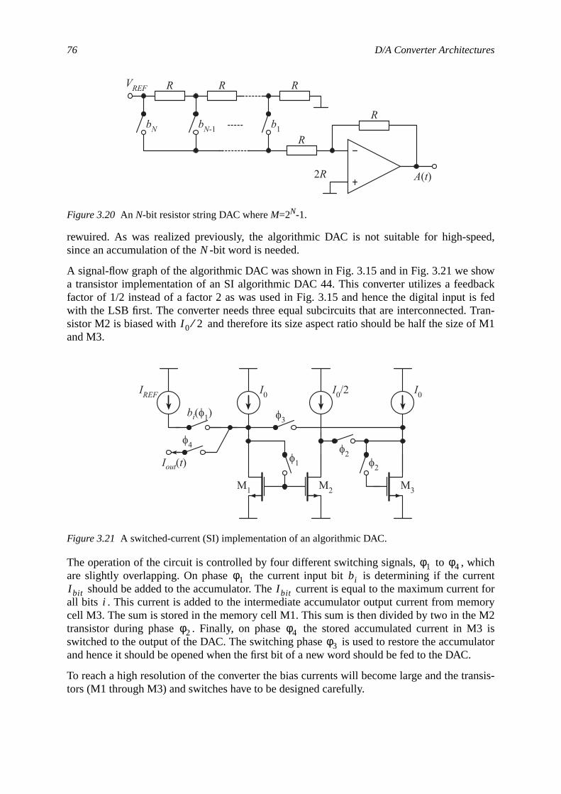
76 D/A Converter Architectures
eed,
owack
is fedTran-f M1
ichrentnt formoryM23 is
ulator.
ansis-
rewuired. As was realized previously, the algorithmic DAC is not suitable for high-spsince an accumulation of the -bit word is needed.
A signal-flow graph of the algorithmic DAC was shown in Fig. 3.15 and in Fig. 3.21 we sha transistor implementation of an SI algorithmic DAC 44. This converter utilizes a feedbfactor of 1/2 instead of a factor 2 as was used in Fig. 3.15 and hence the digital inputwith the LSB first. The converter needs three equal subcircuits that are interconnected.sistor M2 is biased with and therefore its size aspect ratio should be half the size oand M3.
The operation of the circuit is controlled by four different switching signals, to , whare slightly overlapping. On phase the current input bit is determining if the cur
should be added to the accumulator. The current is equal to the maximum curreall bits . This current is added to the intermediate accumulator output current from mecell M3. The sum is stored in the memory cell M1. This sum is then divided by two in thetransistor during phase . Finally, on phase the stored accumulated current in Mswitched to the output of the DAC. The switching phase is used to restore the accumand hence it should be opened when the first bit of a new word should be fed to the DAC
To reach a high resolution of the converter the bias currents will become large and the trtors (M1 through M3) and switches have to be designed carefully.
Figure 3.20 An N-bit resistor string DAC whereM=2N-1.
Figure 3.21 A switched-current (SI) implementation of an algorithmic DAC.
R
A(t)
bN bN-1 b1
2R
R R R
R
VREF
N
I 0 2⁄
Iout(t)
I0 I0I0/2
M1 M2 M3
bi(f1)
IREF
f4
f3
f1
f2f2
φ1 φ4φ1 bi
I bit I biti
φ2 φ4φ3

DAC Comparison 77
ut thehitec-
ell asveralcon-nt the
al fre-gnalto theuse a
ual toor thefre-
ever, aist ofrcuit
onsid-. This
the
s inan begner’s
3.7 DAC ComparisonIn this section we conclude the properties of the DAC architectures discussed througochapter. We compile in tables and figures the properties of different DAC types and arctures as well as reported performance in literature.
In Fig. 3.22 we compile the measured and reported performance from literature as winformation from commercial manufacturers. As we underlined in Chapter 2 there are sedifferent means of performance and resolution. Although the true performance of theverter is not determined by only few measured SFDR or SNDR, we have chosen to preseperformance by using the SFDR and sample frequency in (a) and the SFDR and signquency in (b). For example, with reported performance of 70 dB SFDR at 125 MHz (sifrequency), the measured and reported SFDR is considered to be 70 dB or more upspecified frequency for the specific update frequency. Also notice that we have chosen tologarithmic scale for the signal frequency in Fig. 3.22 (b).
For some of the reported Nyquist-rate converters, the useable signal bandwidth is not eqhalf the update frequency, hence interpolation DACs, and naturally, this is also the case fOSDACs. A better view would be to consider SFDR/SNDR for both signal and updatequencies, hence each point in Fig. 3.22 should be determiend by the three values. Howthree-dimensional plot is not easily interpreted. Therefore, in Table 3.3. we also give a lthe DACs used in the summary together with a description of the DAC architecture, citechnique, etc.
To conclude the reported performance shown in Fig. 3.22 and Table 3.3 we have also cered a best-fit line to the sampled data. This line is given by a slope of -16 dB/decadefigure was briefly mentioned in the previous chapter and we will also touch upon this innext two chapters as well.
From the figures and table we find different design limitations for different architectureterms of speed, resolution, dominating limitations, complexity, and chip area. The table cused as a quick reference guide for proper choice of converter architecture for the desispecific application.
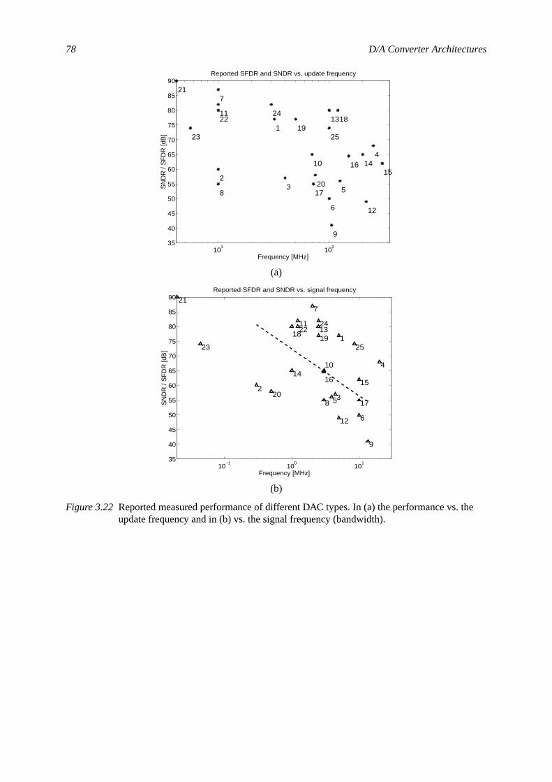
78 D/A Converter Architectures
the
(a)
(b)
Figure 3.22 Reported measured performance of different DAC types. In (a) the performance vs. update frequency and in (b) vs. the signal frequency (bandwidth).
101
102
35
40
45
50
55
60
65
70
75
80
85
90
1
23
4
5
6
7
8
9
10
11
12
13
1415
16
17
1819
20
21
22
23
24
25
Reported SFDR and SNDR vs. update frequency
Frequency [MHz]
SN
DR
/ S
FD
R [d
B]
10−1
100
101
35
40
45
50
55
60
65
70
75
80
85
90
1
23
4
5
6
7
8
9
10
11
12
13
141516
17
1819
20
21
22
23
24
25
Reported SFDR and SNDR vs. signal frequency
Frequency [MHz]
SN
DR
/ S
FD
R [d
B]
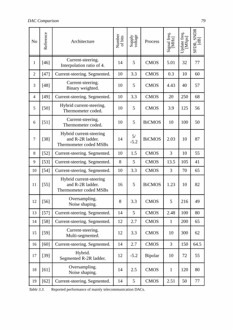
DAC Comparison 79
5
No Architecture Process
1 [46]Current-steering.
Interpolation ratio of 4.14 5 CMOS 5.01 32 77
2 [47] Current-steering. Segmented. 10 3.3 CMOS 0.3 10 60
3 [48]Current-steering.Binary weighted.
10 5 CMOS 4.43 40 57
4 [49] Current-steering. Segmented. 10 3.3 CMOS 20 250 68
5 [50]Hybrid current-steering.
Thermometer coded.10 5 CMOS 3.9 125 56
6 [51]Current-steering.
Thermometer coded.10 5 BiCMOS 10 100 50
7 [38]Hybrid current-steering
and R-2R ladder.Thermometer coded MSBs
145/
-5.2BiCMOS 2.03 10 87
8 [52] Current-steering. Segmented. 10 1.5 CMOS 3 10 55
9 [53] Current-steering. Segmented. 8 5 CMOS 13.5 105 41
10 [54] Current-steering. Segmented. 10 3.3 CMOS 3 70 65
11 [55]Hybrid current-steering
and R-2R ladder.Thermometer coded MSBs
16 5 BiCMOS 1.23 10 82
12 [56]Oversampling.Noise shaping.
8 3.3 CMOS 5 216 49
13 [57] Current-steering. Segmented. 14 5 CMOS 2.48 100 80
14 [58] Current-steering. Segmented. 12 2.7 CMOS 1 200 65
15 [59]Current-steering.Multi-segmented.
12 3.3 CMOS 10 300 62
16 [60] Current-steering. Segmented. 14 2.7 CMOS 3 150 64.
17 [39]Hybrid.
Segmented R-2R ladder.12 -5.2 Bipolar 10 72 55
18 [61]Oversampling.Noise shaping.
14 2.5 CMOS 1 120 80
19 [62] Current-steering. Segmented. 14 5 CMOS 2.51 50 77
Table 3.3. Reported performance of mainly telecommunication DACs.
Ref
eren
ce
Num
ber
of b
its
Sup
ply
volta
ge
Sig
nal f
req.
[MH
z]
Upd
ate
freq
.[M
Sps
]
SF
DR
, SN
DR
[dB
]
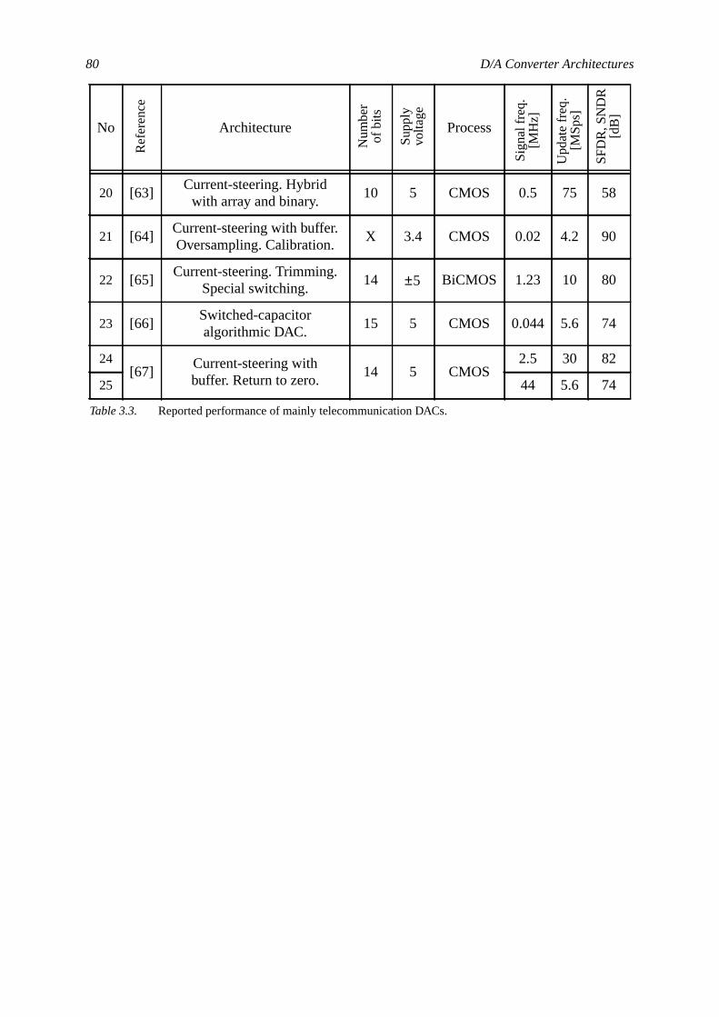
80 D/A Converter Architectures
20 [63]Current-steering. Hybrid
with array and binary.10 5 CMOS 0.5 75 58
21 [64]Current-steering with buffer.Oversampling. Calibration.
X 3.4 CMOS 0.02 4.2 90
22 [65]Current-steering. Trimming.
Special switching.14 BiCMOS 1.23 10 80
23 [66]Switched-capacitoralgorithmic DAC.
15 5 CMOS 0.044 5.6 74
24[67]
Current-steering withbuffer. Return to zero.
14 5 CMOS2.5 30 82
25 44 5.6 74
No Architecture Process
Table 3.3. Reported performance of mainly telecommunication DACs.
Ref
eren
ce
Num
ber
of b
its
Sup
ply
volta
ge
Sig
nal f
req.
[MH
z]
Upd
ate
freq
.[M
Sps
]
SF
DR
, SN
DR
[dB
]
5±
nce ofeters,
umberanu-
rame-
ansis--con-
ncingrties ofstab-
. We
highto
4 Behavioral-Level Modelsfor Current-Steering,
Nyquist-Rate D/A Converters4.1 IntroductionIn this chapter we present proposed models and methodology to predict the performaunbuffered current-steering DACs. We show how the distortion and noise relate to paramsuch as the output impedance, matching error, and circuit noise. The work results in a nof compact formulas that can be used to relatively quick estimate the performance of a mfactured chip. The proposed formulas also give us a design guide for finding proper paters during the design phase.
The design of high-accuracy integrated circuits highly depends on the models used for trtors and other comonents. Characterization of semi-conductors is a complex and timesuming work. For small-dimension transistors complex short-channel effects are influethe results more and more. The models must be able to handle three-dimensional propethe layout. For the transistors, for example, the BSIM level 3 models are now well-elished, but the work to refine and improve the model is continuous.
In general, in terms of abstraction, there are several levels of modeling of the circuitshave for example in descending order from high level of abstraction:
• behavioral level: simulation with AHDL, Matlab, C, etc.• circuit or transistor level: simulation with Spice, Spectre, etc.• layout level: simulation with Spice or Spectre of the extracted layout
view, including parasitic components from nonideal interconnection wires
The lower level of abstraction, the more parameters we include in the models. Due to thecomplexity of a D/A converter or in general, a mixed-signal circuit, it is important not only
81
82 Behavioral-Level Models for Current-Steering, Nyquist-Rate D/A Converters
i.e., weel andls arenfor-ircuiton-st alsoe.g.,rove-nera-ously
dis-utputned ine fre-uch as
L ismoressed
c andwhichic ares, timerfor-ertiese must
ig. 4.1,hapteralizedce the
ped-erefore
off-
have good, accurate models. For the designer, they should also be understandable,want to relatively easy be able to extract fundamental design parameters from the modunderstand how these limit the performance. For this purpose, the circuit and layout levemuch to detailed. We want to be able to work with models where we can add sufficient imation to be able to extract for example the influence of noise, nonlinearity, and other cimperfections. It is important to know in advance how the converter will react on circuit nidealities, to be able to avoid these errors during the design and layout phases. We muknow if the errors will give rise to additional noise or cause a nonlinear transfer function,distortion? The models also help us to identify bottle-necks and how to find possible impment techniques. Using for example Matlab or C we also have a flexible tools where getion of new architectures, stimuli, etc., becomes fairly easy. The models are continuverified and refined using the results from measurements and simulations.
We present an overview of some different models of Nyquist-rate DACs. Especially, wecuss how specific circuit errors such as for example device matching errors, finite oimpedance, settling errors, etc., affect the performance of the converter. As was mentioChapter 2, most of the characterization of the performance of converters is done in thquency domain. Therefore, these models also result in frequency-domain measures, sthe SNDR, SNR, and SFDR. However, the impact of typical DAC errors on DNL and INalso briefly discussed in the chapter. Previously reported models of DAC errors havebeen focused on INL and DNL requirements, and only few of them have thoroughly discuthe impact of DAC errors on the frequency-domain and dynamic parameters.
The models can, as well as the performance characterization, be divided into statidynamic error models. Roughly, the static models describe the settled output values, (often are too optimistic and do not determine the true performance), and the dynamgiven by the signal-dependent transition between two states, hence the slewing, glitcheskew, etc. In communications and wideband applications it is mostly the dynamic pemance that determines the overall quality of the converter. But generally, the static propset the best-case performance and, naturally, to achieve a good dynamic performance walso guarantee a good static performance.
Since the current-steering DAC structure, as presented in Sec. 3.6.1 and repictured in Fis a suitable candidate for high-speed applications, the models proposed in this cdescribe the operation of this type of DAC. However, some of the models can be generto cover other architectures as well. Process variations and other parasitics will influenmatching between current sources and will introduce noise and distortion. The output imance is depedendent on the number of current sources connected to the output and is thit becomes signal-dependent. In Fig. 4.1 we show a typical current-steering DAC.
Briefly, we repeat the operation of the current-steering DAC as illustrated in by the -bitset binary-weighted DAC in Fig. 4.1. The output current is given by
, (4.1)
where is the digital input given by
(4.2)
N
I out X( ) 2N 1– I LSB bN⋅ … 2I LSB b2⋅ I LSB b1⋅+ + + I LSB X⋅= =
X
X 2N 1– bN⋅ 2 b2⋅ … b1+ + + 2m 1– bm⋅m 0=
N
∑= =
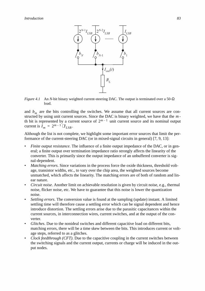
Introduction 83
con-e -utput
per-
n-hesig-
olt-
d lin-
aln
edhence theon-
volt-
en out-
and are the bits controlling the switches. We assume that all current sources arestructed by using unit current sources. Since the DAC is binary weighted, we have that thth bit is represented by a current source of unit current source and its nominal ocurrent is .
Although the list is not complete, we highlight some important error sources that limit theformance of the current-steering DAC (or in mixed-signal circuits in general) [7, 9, 13]:
• Finite output resistance. The influence of a finite output impedance of the DAC, or in geeral; a finite output over termination impedance ratio strongly affects the linearity of tconverter. This is primarily since the output impedance of an unbuffered converter is nal-dependent.
• Matching errors. Since variations in the process force the oxide thickness, threshold vage, transistor widths, etc., to vary over the chip area, the weighted sources becomeunmatched, which affects the linearity. The matching errors are of both of random anear nature.
• Circuit noise. Another limit on achievable resolution is given by circuit noise, e.g., thermnoise, flicker noise, etc. We have to guarantee that this noise is lower the quantizationoise.
• Settling errors. The conversion value is found at the sampling (update) instant. A limitsettling time will therefore cause a settling error which can be signal dependent and introduce distortion. The settling errors arise due to the parasitic capacitances withincurrent sources, in interconnection wires, current switches, and at the output of the cverter.
• Glitches. Due to the nonideal switches and different capacitive load on different bits,matching errors, there will be a time skew between the bits. This introduces current orage steps, referred to as a glitches.
• Clock feedthrough (CFT). Due to the capacitive coupling in the current switches betwethe switching signals and the current output, currents or charge will be induced in theput nodes.
Figure 4.1 An N-bit binary weighted current-steering DAC. The output is terminated over a 50-Ωload.
ILSB2N-1ILSB 2N-2ILSB
bN bN-1 b1
Iout(t)
RL
bmm
2m 1–
I m 2m 1– I LSB⋅=
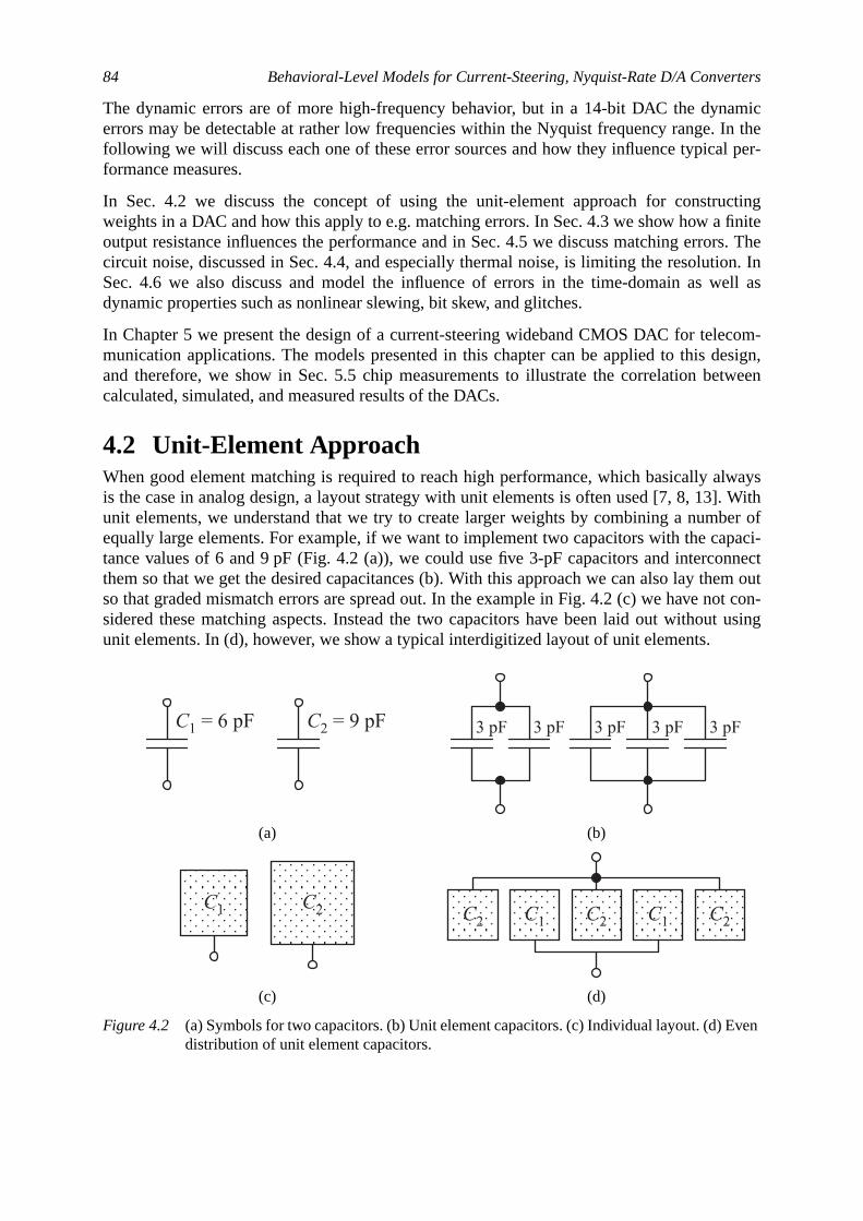
84 Behavioral-Level Models for Current-Steering, Nyquist-Rate D/A Converters
amicIn thel per-
ctingfiniters. Then. Inell as
com-esign,tween
lways. Withber ofpaci-nnectem outt con-
t using
ven
The dynamic errors are of more high-frequency behavior, but in a 14-bit DAC the dynerrors may be detectable at rather low frequencies within the Nyquist frequency range.following we will discuss each one of these error sources and how they influence typicaformance measures.
In Sec. 4.2 we discuss the concept of using the unit-element approach for construweights in a DAC and how this apply to e.g. matching errors. In Sec. 4.3 we show how aoutput resistance influences the performance and in Sec. 4.5 we discuss matching errocircuit noise, discussed in Sec. 4.4, and especially thermal noise, is limiting the resolutioSec. 4.6 we also discuss and model the influence of errors in the time-domain as wdynamic properties such as nonlinear slewing, bit skew, and glitches.
In Chapter 5 we present the design of a current-steering wideband CMOS DAC for telemunication applications. The models presented in this chapter can be applied to this dand therefore, we show in Sec. 5.5 chip measurements to illustrate the correlation becalculated, simulated, and measured results of the DACs.
4.2 Unit-Element ApproachWhen good element matching is required to reach high performance, which basically ais the case in analog design, a layout strategy with unit elements is often used [7, 8, 13]unit elements, we understand that we try to create larger weights by combining a numequally large elements. For example, if we want to implement two capacitors with the catance values of 6 and 9 pF (Fig. 4.2 (a)), we could use five 3-pF capacitors and intercothem so that we get the desired capacitances (b). With this approach we can also lay thso that graded mismatch errors are spread out. In the example in Fig. 4.2 (c) we have nosidered these matching aspects. Instead the two capacitors have been laid out withouunit elements. In (d), however, we show a typical interdigitized layout of unit elements.
(a) (b)
(c) (d)
Figure 4.2 (a) Symbols for two capacitors. (b) Unit element capacitors. (c) Individual layout. (d) Edistribution of unit element capacitors.
C1 = 6 pF C2 = 9 pF 3 pF 3 pF 3 pF 3 pF 3 pF
C1 C2 C1C2 C1C2 C2
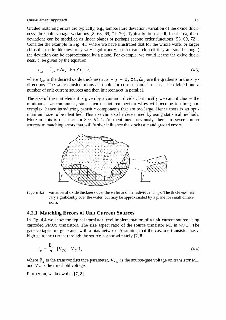
Unit-Element Approach 85
thick-these, 72] .
argerugh)thick-
-into a
e theand
n opti-thods.other
sing. Ther has a
or M1,
ayn-
Graded matching errors are typically, e.g., temperature deviation, variation of the oxideness, threshold voltage variations [8, 68, 69, 71, 70]. Typically, in a small, local area,deviations can be modelled as linear planes or perhaps second order functions [53, 69Consider the example in Fig. 4.3 where we have illustrated that for the whole wafer or lchips the oxide thickness may vary significantly, but for each chip (if they are small enothe deviation can be approximated by a plane. For example, we could let the the oxideness, , be given by the equation
, (4.3)
where is the desired oxide thickness at , are the gradients in thedirections. The same considerations also hold for current sources that can be dividednumber of unit current sources and then interconnect in parallel.
The size of the unit element is given by a common divider, but mostly we cannot choosminimum size component, since then the interconnection wires will become too longcomplex, hence introducing parasitic components that are too large. Hence there is amum unit size to be identified. This size can also be determined by using statistical meMore on this is discussed in Sec. 5.2.1. As mentioned previously, there are severalsources to matching errors that will further influence the stochastic and graded errors.
4.2.1 Matching Errors of Unit Current SourcesIn Fig. 4.4 we show the typical transistor-level implementation of a unit current source ucascoded PMOS transistors. The size aspect ratio of the source transistor M1 isgate voltages are generated with a bias network. Assuming that the cascode transistohigh gain, the current through the source is approximately [7, 8]
, (4.4)
where is the transconductance parameter, is the source-gate voltage on transistand is the threshold voltage.
Further on, we know that [7, 8]
Figure 4.3 Variation of oxide thickness over the wafer and the individual chips. The thickness mvary significantly over the wafer, but may be approximated by a plane for small dimesions.
t
tox tox ∆tx x⋅ ∆ty y⋅+ +=
tox x y 0= = ∆tx ∆ty, x y,
W L⁄
I u
βu
2----- VSG VT–( )2⋅=
βu VSGVT
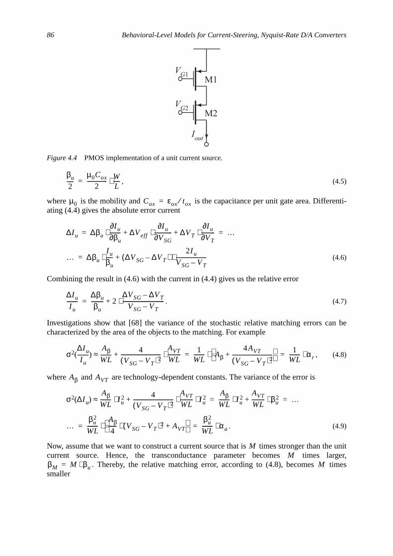
86 Behavioral-Level Models for Current-Steering, Nyquist-Rate D/A Converters
nti-
an be
e unitlarger,mes
, (4.5)
where is the mobility and is the capacitance per unit gate area. Differeating (4.4) gives the absolute error current
(4.6)
Combining the result in (4.6) with the current in (4.4) gives us the relative error
. (4.7)
Investigations show that [68] the variance of the stochastic relative matching errors ccharacterized by the area of the objects to the matching. For example
, (4.8)
where and are technology-dependent constants. The variance of the error is
. (4.9)
Now, assume that we want to construct a current source that is times stronger than thcurrent source. Hence, the transconductance parameter becomes times
. Thereby, the relative matching error, according to (4.8), becomes tismaller
Figure 4.4 PMOS implementation of a unit current source.
VG1
VG2
Iout
M1
M2
βu
2-----
µ0Cox
2--------------- W
L-----⋅=
µ0 Cox εox tox⁄=
∆I u ∆βu
I u∂βu∂
--------⋅ ∆Veff
I u∂VSG∂
-------------⋅ ∆VT
I u∂VT∂
----------⋅+ + …= =
… ∆βu
I u
βu-----⋅ ∆VSG ∆VT–( )
2I u
VSG VT–-----------------------⋅+=
∆I u
I u--------
∆βu
βu--------- 2
∆VSG ∆VT–
VSG VT–-------------------------------⋅+=
σ2∆I u
I u--------( )
AβWL--------
4VSG VT–( )2
------------------------------AVT
WL----------⋅+≈ 1
WL-------- Aβ
4AVT
VSG VT–( )2------------------------------+
⋅ 1WL-------- αr⋅= =
Aβ AVT
σ2 ∆I u( )AβWL-------- I u
2⋅ 4VSG VT–( )2
------------------------------AVT
WL---------- I u
2⋅ ⋅+≈AβWL-------- I u
2⋅AVT
WL---------- βu
2⋅+ …= =
…βu
2
WL--------
Aβ4
------ VSG VT–( )2⋅ AVT+ ⋅
βu2
WL-------- αa⋅= =
MM
βM M βu⋅= M
Limited Output Impedance 87
g thatiance
asticach.
niquesf the
usingorter as
e tran-rs thes pos-sense
i.e.,
w aodede. The
rrents,tslow-tput
er aree cur-
acrossnsiderances have
(4.10)
and the absolute error according to (4.9) becomes times larger
. (4.11)
If we would use unit elements instead, we should use unit current sources. Assuminthe stochastic matching errors, , are individually independent, we may find the var
. (4.12)
Comparing the result in (4.12) with the one in (4.11) we see that considering stochmatching errors, we actually do not gain in matching by using the unit element approThere are however, advantages in terms of the possibilities to use special layout techsuch as interdigitized or common-centroid. Thereby we can minimize the influence ograded matching errors. Secondly, we are also able to achieve a better edge matchingunit elements and the distance between transistors that should be matched becomes shwell. We can include this distance in the formulas above [68] and we get for example
, (4.13)
where is a process- and bias-dependent constant and is the distance between thsistors (or objects) to match. We see that with a larger distance between the transistomismatch increases. Therefore, we should obviously try to keep this distance as small asible. If we lay the transistors out as dense as possible, the distance will also in somedetermined by the transistor sizes. The larger transistors the larger distance,
.
4.3 Limited Output ImpedanceFirst, we consider a dual-output (differential) current-steering DAC. In Fig. 4.5 we shotypical implementation, where the current sources typically are implemented by casctransistors as in Fig. 4.4. The cascodes are used to increase the output impedancswitches are implemented with MOS transistors or transmission gates. The output cu
and , are terminated by 50-Ω loads . In some applications, the output currenare fed to an output buffer which provides the DAC with a virtual ground and hence aimpedance load. This significantly improves the linearity with respect to the limited ouimpedance. However, the buffer itself may limit the performance instead.
The switch signals are slightly overlapping to guarantee that the current sources nevcompletely turned off which would have given glitches and a slower startup phase as thrent sources are opened again. The transistors are dependent on the voltage appliedthem, i.e., the drain-source voltage, hence they will have a finite output impedance. Cothe linearized model of the DAC shown in Fig. 4.6. We have the limited output conductof the current source as well as parasitic capacitance. The switch and interconnect wire
σ2 ∆I M I M⁄( )1
WL( ) M⋅----------------------- αr⋅≈
σ2 ∆I u I u⁄( )
M---------------------------=
M
σ2 ∆I M( )βM
2
WL( ) M⋅----------------------- αa⋅≈
M βu2⋅
WL( )--------------- αr⋅ M σ2 ∆I u( )⋅= =
M∆I u m,
E ∆I u m,m 1=
M
∑ 2
E ∆I u m,2
m 1=
M
∑ M σ2 ∆I u( )⋅= =
σ2 ∆I u( )βu
2
WL-------- αa⋅ βu
2 αd D2⋅ ⋅+=
αd D
D
D a W⋅ b L⋅+∼
I out+ I out
– GL( )
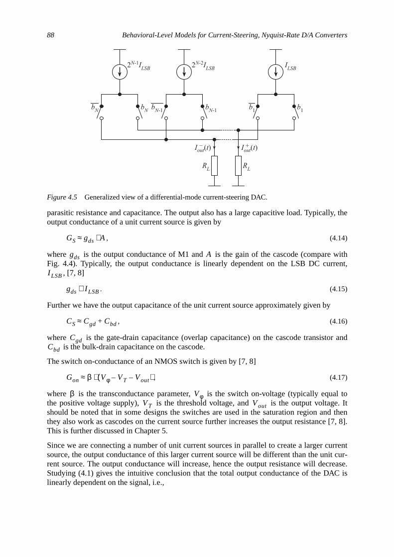
88 Behavioral-Level Models for Current-Steering, Nyquist-Rate D/A Converters
lly, the
withrent,
y
tor and
al toe. Itd then
e [7, 8].
urrentit cur-rease.C is
parasitic resistance and capacitance. The output also has a large capacitive load. Typicaoutput conductance of a unit current source is given by
, (4.14)
where is the output conductance of M1 and is the gain of the cascode (compareFig. 4.4). Typically, the output conductance is linearly dependent on the LSB DC cur
, [7, 8]
. (4.15)
Further we have the output capacitance of the unit current source approximately given b
, (4.16)
where is the gate-drain capacitance (overlap capacitance) on the cascode transis is the bulk-drain capacitance on the cascode.
The switch on-conductance of an NMOS switch is given by [7, 8]
, (4.17)
where is the transconductance parameter, is the switch on-voltage (typically equthe positive voltage supply), is the threshold voltage, and is the output voltagshould be noted that in some designs the switches are used in the saturation region anthey also work as cascodes on the current source further increases the output resistancThis is further discussed in Chapter 5.
Since we are connecting a number of unit current sources in parallel to create a larger csource, the output conductance of this larger current source will be different than the unrent source. The output conductance will increase, hence the output resistance will decStudying (4.1) gives the intuitive conclusion that the total output conductance of the DAlinearly dependent on the signal, i.e.,
Figure 4.5 Generalized view of a differential-mode current-steering DAC.
ILSB2N-1ILSB 2N-2ILSB
bN bN-1 b1
Iout(t)
RL
bN-1bN b1
RL
Iout(t)
GS gds A⋅≈
gds A
I LSB
gds I LSB∼
CS Cgd Cbd+≈
CgdCbd
Gon β Vφ VT– Vout–( )⋅≈
β VφVT Vout
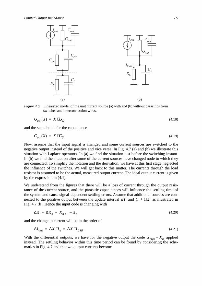
Limited Output Impedance 89
to thee thistant.h theylectedload
s given
resis-me ofre con-
ed in
liedsche-
(4.18)
and the same holds for the capacitance
. (4.19)
Now, assume that the input signal is changed and some current sources are switchednegative output instead of the positive and vice versa. In Fig. 4.7 (a) and (b) we illustratsituation with Laplace operators. In (a) we find the situation just before the switching insIn (b) we find the situation after some of the current sources have changed node to whicare connected. To simplify the notation and the derivation, we have at this first stage negthe influence of the switches. We will get back to this matter. The currents through theresistor is assumed to be the actual, measured output current. The ideal output current iby the expression in (4.1).
We understand from the figures that there will be a loss of current through the outputtance of the current source, and the parasitic capacitances will influence the settling tithe system and cause signal-dependent settling errors. Assume that additional sources anected to the positive output between the update interval and as illustratFig. 4.7 (b). Hence the input code is changing with
(4.20)
and the change in current will be in the order of
. (4.21)
With the differential outputs, we have for the negative output the code appinstead. The settling behavior within this time period can be found by considering thematics in Fig. 4.7 and the two output currents become
(a) (b)
Figure 4.6 Linearized model of the unit current source (a) with and (b) without parasitics fromswitches and interconnection wires.
Iout
Gout
Cout
Gon
Csw
CLRL
Iout
Gout
Cout
CLRL
Iload
Gout X( ) X GS⋅=
Cout X( ) X CS⋅=
nT n 1+( )T
∆X ∆Xn Xn 1+ Xn–= =
∆I out ∆X Iu⋅ ∆X ILSB⋅= =
Xmax Xn–
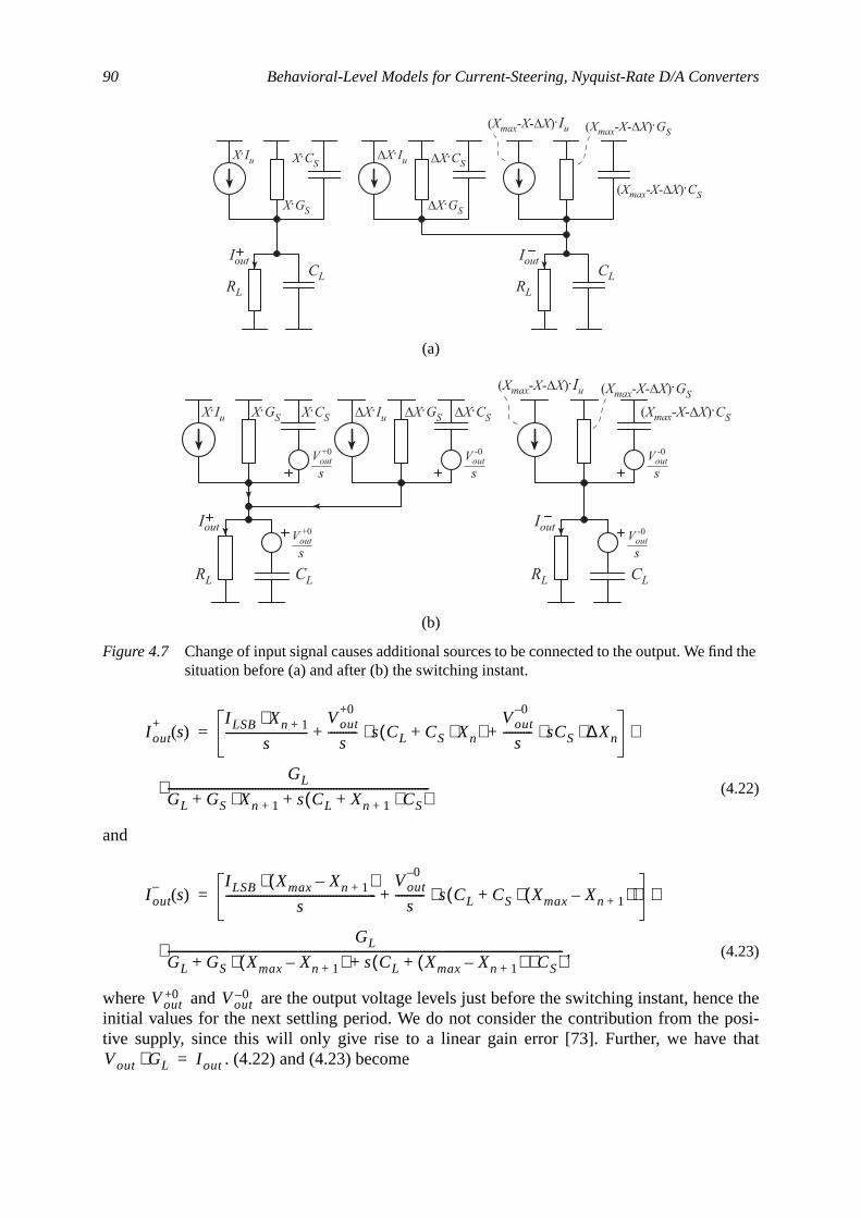
90 Behavioral-Level Models for Current-Steering, Nyquist-Rate D/A Converters
e theosi-that
nd the
(4.22)
and
, (4.23)
where and are the output voltage levels just before the switching instant, hencinitial values for the next settling period. We do not consider the contribution from the ptive supply, since this will only give rise to a linear gain error [73]. Further, we have
. (4.22) and (4.23) become
(a)
(b)
Figure 4.7 Change of input signal causes additional sources to be connected to the output. We fisituation before (a) and after (b) the switching instant.
CLRL
CLRL
IoutIout
X.CS
X.GS
X.Iu DX.Iu
DX.GS
DX.CS
(Xmax-X-DX).GS(Xmax-X-DX).Iu
(Xmax-X-DX).CS
CLRL
IoutIout
CLRL
X.CSX.GSX.Iu DX.Iu DX.GS DX.CS
Vout+0
s
Vout+0
sVout
-0
s
Vout-0
s
Vout-0
s
(Xmax-X-DX).GS(Xmax-X-DX).Iu
(Xmax-X-DX).CS
I out+
s( )I LSB Xn 1+⋅
s----------------------------
Vout+0
s---------- s CL CS Xn⋅+( )⋅
Vout–0
s---------- sCS ∆Xn⋅⋅+ + ⋅=
GL
GL GS Xn 1+⋅ s CL Xn 1+ CS⋅+( )+ +------------------------------------------------------------------------------------------⋅
I out–
s( )I LSB Xmax Xn 1+–( )⋅
s----------------------------------------------------
Vout–0
s---------- s CL CS Xmax Xn 1+–( )⋅+( )⋅+ ⋅=
GL
GL GS Xmax Xn 1+–( )⋅ s CL Xmax Xn 1+–( ) CS⋅+( )+ +-----------------------------------------------------------------------------------------------------------------------------------------⋅
Vout+0 Vout
–0
Vout GL⋅ I out=
Limited Output Impedance 91
thecon-
pplied
on
(4.24)
and
(4.25)
where and denote the output current values just beforeswitching instant. In (4.24) and (4.25) we identify the load and unit current source timestants
and . (4.26)
Notice that the settling time constant of the current sources is independent on the code aon the DAC. We have
. (4.27)
The conductance and capacitance ratios are given by
and . (4.28)
We define the signal-dependent system time constant as
. (4.29)
The output currents from (4.24) and (4.25) can now be written
(4.30)
and
(4.31)
We find expressions on the currents in the time domain for and we use the notati
I out+
s( )I LSB Xn 1+⋅
s---------------------------- I out
+ CL CS Xn⋅+
GL-------------------------------⋅ I out
– CS
GL------- ∆Xn⋅ ⋅+ + ⋅=
11 GS GL⁄ Xn 1+⋅+--------------------------------------------- 1 s
CL CS Xn 1+⋅+
GL GS Xn 1+⋅+--------------------------------------+⁄⋅
I out–
s( )I LSB Xmax Xn 1+–( )
s----------------------------------------------- I out
– CL CS Xmax Xn 1+–( )+
GL---------------------------------------------------------⋅+ ⋅=
11 GS GL⁄ Xmax Xn 1+–( )⋅+-------------------------------------------------------------------- 1 s
CL CS Xmax Xn 1+–( )⋅+
GL GS Xmax Xn 1+–( )⋅+-------------------------------------------------------------+⁄⋅
I out+
Vout+0
GL⋅= I out–
Vout–0
GL⋅=
τL CL GL⁄= τS CS GS⁄=
τS X( )X CS⋅X GS⋅---------------
CS
GS------ τS= = =
ρG GS GL⁄= ρC CS CL⁄=
τσ X( ) τL
1 ρC X⋅+
1 ρG X⋅+------------------------⋅=
I out+
s( )I LSB Xn 1+⋅
s---------------------------- I out
+ τL⋅ 1 ρC Xn⋅+( )⋅ I out– τL ρC ∆Xn⋅ ⋅ ⋅+ + ⋅=
11 ρG Xn 1+⋅+---------------------------------- 1 s τσ Xn 1+( )⋅+[ ]⁄⋅
I out–
s( )I LSB Xmax Xn 1+–( )⋅
s---------------------------------------------------- I out
– τL⋅ 1 ρC Xmax Xn 1+–( )+( )⋅+ ⋅=
11 ρG Xmax Xn 1+–( )⋅+--------------------------------------------------------- 1 s τσ Xmax Xn 1+–( )⋅+[ ]⁄⋅
t nT≥
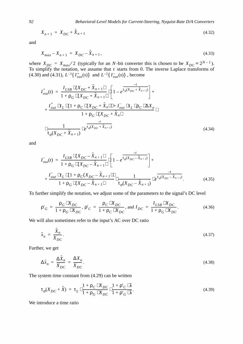
92 Behavioral-Level Models for Current-Steering, Nyquist-Rate D/A Converters
).s of
el
(4.32)
and
, (4.33)
where (typically for an -bit converter this is chosen to beTo simplify the notation, we assume that starts from 0. The inverse Laplace transform(4.30) and (4.31), and , become
(4.34)
and
. (4.35)
To further simplify the notation, we adjust some of the parameters to the signal’s DC lev
, , and . (4.36)
We will also sometimes refer to the input’s AC over DC ratio
. (4.37)
Further, we get
. (4.38)
The system time constant from (4.29) can be written
. (4.39)
We introduce a time ratio
Xn 1+ XDC Xn 1++=
Xmax Xn 1+– XDC Xn 1+–=
XDC Xmax 2⁄= N XDC 2N 1–≈t
L 1– I out+ s( ) L 1– I out
– s( )
I out+
t( )I LSB XDC Xn 1++( )⋅
1 ρG XDC Xn 1++( )⋅+-------------------------------------------------------- 1 e
t–
τσ XDC Xn 1++( )-----------------------------------------
–⋅ +=
I out+ τL⋅ 1 ρC XDC Xn+( )⋅+( )⋅ I out
– τL ρC ∆Xn⋅ ⋅ ⋅+
1 ρG XDC Xn+( )⋅+--------------------------------------------------------------------------------------------------------------------------------- ⋅+
1
τσ XDC Xn 1++( )---------------------------------------- e
t–
τσ XDC Xn 1++( )-----------------------------------------
⋅ ⋅
I out–
t( )I LSB XDC Xn 1+–( )⋅
1 ρG XDC Xn 1+–( )⋅+-------------------------------------------------------- 1 e
t–
τσ XDC Xn 1+–( )----------------------------------------
–⋅ +=
I out– τL⋅ 1 ρC XDC Xn 1+–( )+( )⋅
1 ρG XDC Xn 1+–( )⋅+-------------------------------------------------------------------------------- 1
τσ XDC Xn 1+–( )---------------------------------------- e
t–
τσ XDC Xn 1+–( )----------------------------------------
⋅ ⋅+
ρ'GρG XDC⋅
1 ρG XDC⋅+-------------------------------= ρ'C
ρC XDC⋅1 ρC XDC⋅+-------------------------------= I DC
I LSB XDC⋅1 ρG XDC⋅+-------------------------------=
xnXn
XDC----------=
∆ xn∆Xn
XDC----------
∆Xn
XDC----------= =
τσ XDC X+( ) τL
1 ρC XDC⋅+
1 ρG XDC⋅+-------------------------------
1 ρ'C x⋅+
1 ρ'G x⋅+------------------------⋅ ⋅=
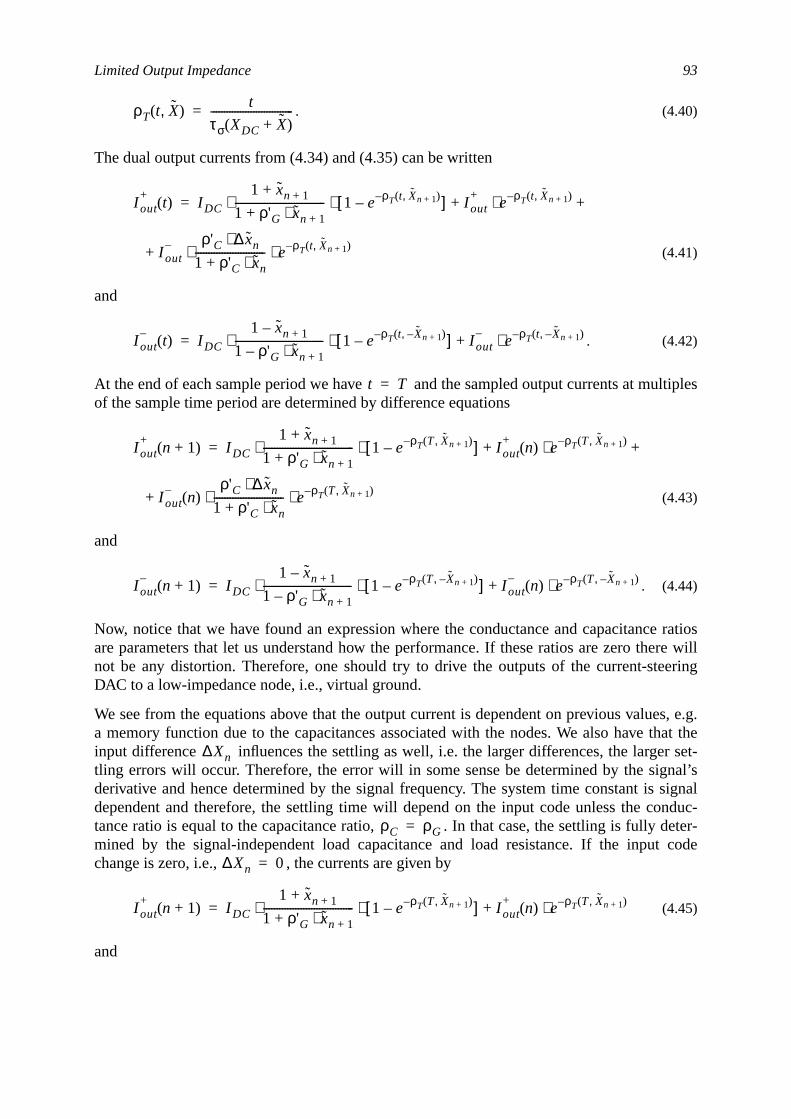
Limited Output Impedance 93
ltiples
ratiosre will
ering
es, e.g.hat ther set-nal’ssignalnduc-eter-code
. (4.40)
The dual output currents from (4.34) and (4.35) can be written
(4.41)
and
. (4.42)
At the end of each sample period we have and the sampled output currents at muof the sample time period are determined by difference equations
(4.43)
and
. (4.44)
Now, notice that we have found an expression where the conductance and capacitanceare parameters that let us understand how the performance. If these ratios are zero thenot be any distortion. Therefore, one should try to drive the outputs of the current-steDAC to a low-impedance node, i.e., virtual ground.
We see from the equations above that the output current is dependent on previous valua memory function due to the capacitances associated with the nodes. We also have tinput difference influences the settling as well, i.e. the larger differences, the largetling errors will occur. Therefore, the error will in some sense be determined by the sigderivative and hence determined by the signal frequency. The system time constant isdependent and therefore, the settling time will depend on the input code unless the cotance ratio is equal to the capacitance ratio, . In that case, the settling is fully dmined by the signal-independent load capacitance and load resistance. If the inputchange is zero, i.e., , the currents are given by
(4.45)
and
ρT t X,( ) t
τσ XDC X+( )-------------------------------=
I out+
t( ) I DC
1 xn 1++
1 ρ'G xn 1+⋅+----------------------------------⋅ 1 e ρT t Xn 1+,( )––[ ]⋅ I out
+e ρT t Xn 1+,( )–⋅+ +=
I out– ρ'C ∆ xn⋅
1 ρ'C xn⋅+--------------------------⋅ e ρT t Xn 1+,( )–⋅+
I out–
t( ) I DC
1 xn 1+–
1 ρ'G xn 1+⋅–---------------------------------⋅ 1 e ρT t Xn 1+–,( )––[ ]⋅ I out
–e ρT t Xn 1+–,( )–⋅+=
t T=
I out+
n 1+( ) I DC
1 xn 1++
1 ρ'G xn 1+⋅+---------------------------------- 1 e ρT T Xn 1+,( )––[ ]⋅ ⋅ I out
+n( ) e ρT T Xn 1+,( )–⋅+ +=
I out–
n( )ρ'C ∆ xn⋅
1 ρ'C xn⋅+--------------------------⋅ e ρT T Xn 1+,( )–⋅+
I out–
n 1+( ) I DC
1 xn 1+–
1 ρ'G xn 1+⋅–--------------------------------- 1 e ρT T Xn 1+–,( )––[ ]⋅ ⋅ I out
–n( ) e ρT T Xn 1+–,( )–⋅+=
∆Xn
ρC ρG=
∆Xn 0=
I out+
n 1+( ) I DC
1 xn 1++
1 ρ'G xn 1+⋅+---------------------------------- 1 e ρT T Xn 1+,( )––[ ]⋅ ⋅ I out
+n( ) e ρT T Xn 1+,( )–⋅+=
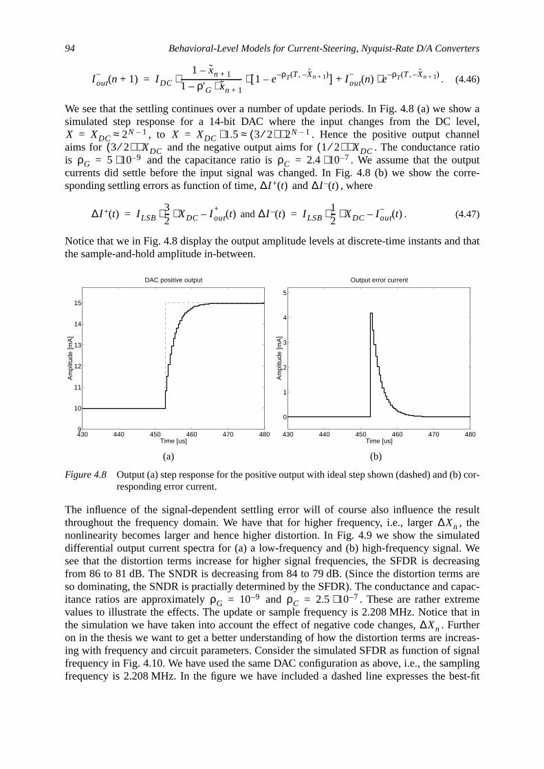
94 Behavioral-Level Models for Current-Steering, Nyquist-Rate D/A Converters
how alevel,l
atiotputorre-
d that
esult, thelated. Weeasings areapac-emeat in
urthercreas-ignalpling
est-fit
) cor-
. (4.46)
We see that the settling continues over a number of update periods. In Fig. 4.8 (a) we ssimulated step response for a 14-bit DAC where the input changes from the DC
, to . Hence the positive output channeaims for and the negative output aims for . The conductance ris and the capacitance ratio is . We assume that the oucurrents did settle before the input signal was changed. In Fig. 4.8 (b) we show the csponding settling errors as function of time, and , where
and . (4.47)
Notice that we in Fig. 4.8 display the output amplitude levels at discrete-time instants anthe sample-and-hold amplitude in-between.
The influence of the signal-dependent settling error will of course also influence the rthroughout the frequency domain. We have that for higher frequency, i.e., largernonlinearity becomes larger and hence higher distortion. In Fig. 4.9 we show the simudifferential output current spectra for (a) a low-frequency and (b) high-frequency signalsee that the distortion terms increase for higher signal frequencies, the SFDR is decrfrom 86 to 81 dB. The SNDR is decreasing from 84 to 79 dB. (Since the distortion termso dominating, the SNDR is practially determined by the SFDR). The conductance and citance ratios are approximately and . These are rather extrvalues to illustrate the effects. The update or sample frequency is 2.208 MHz. Notice ththe simulation we have taken into account the effect of negative code changes, . Fon in the thesis we want to get a better understanding of how the distortion terms are ining with frequency and circuit parameters. Consider the simulated SFDR as function of sfrequency in Fig. 4.10. We have used the same DAC configuration as above, i.e., the samfrequency is 2.208 MHz. In the figure we have included a dashed line expresses the b
(a) (b)
Figure 4.8 Output (a) step response for the positive output with ideal step shown (dashed) and (bresponding error current.
I out–
n 1+( ) I DC
1 xn 1+–
1 ρ'G xn 1+⋅–--------------------------------- 1 e ρT T Xn 1+–,( )––[ ]⋅ ⋅ I out
–n( ) e ρT T Xn 1+–,( )–⋅+=
X XDC 2N 1–≈= X XDC 1.5⋅ 3 2⁄( ) 2N 1–⋅≈=3 2⁄( ) XDC⋅ 1 2⁄( ) XDC⋅
ρG 5 10 9–⋅= ρC 2.4 10 7–⋅=
∆I + t( ) ∆I – t( )
∆I + t( ) I LSB32--- XDC⋅ ⋅ I out
+t( )–= ∆I – t( ) I LSB
12--- XDC⋅ ⋅ I out
–t( )–=
430 440 450 460 470 4809
10
11
12
13
14
15
DAC positive output
Time [us]
Am
plitu
de [m
A]
430 440 450 460 470 480
0
1
2
3
4
5
Output error current
Time [us]
Am
plitu
de [m
A]
∆Xn
ρG 10 9–= ρC 2.5 10 7–⋅=
∆Xn
Limited Output Impedance 95
ttlingt case
line to the simulated SFDR. The slope of this line is approximately 20 dB/decade.
4.3.1 Settling-Time Error with Ideal Current SourcesAssume that and are very small or even zero. Then we have and the se(and bandwidth) of the system is given by the load capacitance and resistance. In tha(4.42) and (4.43) become
(4.48)
and
. (4.49)
(a) (b)
Figure 4.9 Output spectra for (a) lower and (b) higher signal frequencies.
Figure 4.10 Simulated SFDR as function of signal frequency.
0 0.552 1.104
−118
−72
−36
0
DAC differential output
Frequency [MHz]
Po
we
r [d
B]
0 0.552 1.104
−118
−72
−36
0
DAC differential output
Frequency [MHz]
Po
we
r [d
B]
239 304 387 494 629
70
75
80
85
Simulated SFDR with best−fit line
Signal frequency [kHz]
SF
DR
[dB
]
ρC ρG τσ τL≈
I out+
n 1+( ) I LSB XDC Xn 1++( ) 1 e T τL⁄––[ ]⋅ ⋅ I out+
n( ) e T τL⁄–⋅+=
I out–
n 1+( ) I LSB XDC Xn 1+–( ) 1 e T τL⁄––[ ]⋅ ⋅ I out–
n( ) e T τL⁄–⋅+=

96 Behavioral-Level Models for Current-Steering, Nyquist-Rate D/A Converters
e nor-e ele-at theut-
error
) and
r sys-
the
the
The currents are dependent on the current at the previous sampling instant, which is thmal operation of a system with an impedance containing both resistive and capacitivments. This dependency is determining the bandwidth of the system. If we apply a stepinput the output will settle as shown in Fig. 4.8. If we apply a ramp , the oput current at the sampling instants will be given by
, (4.50)
where the latter approximation holds for larger . We see from (4.50) that the settlingwill stabilize and become independent of .
We get the differential output current as the difference between the dual outputs in (4.48(4.49)
. (4.51)
Using (4.48) and (4.49) in (4.51) gives
. (4.52)
This expression is transformed into the z-domain and we get
. (4.53)
The differential output current from (4.53) can be considered as the output from a lineatem to which the signal has been applied. This system function is identified as
. (4.54)
On the unit circle, we have where is the normalized angular frequency (orangle). We get
. (4.55)
If the input is a sinusoid, e.g. , the signal is an eigenfunction oflinear system and we have the output current given by
. (4.56)
Using (4.55) and (4.56) we can write the squared output current
X 0 1 2 …, , ,=( )
I out+
n( ) I LSB 1 e T τL⁄––( )k 1=
n
∑⋅ n ILSB⋅ I LSB e T τL⁄–⋅ e T τL⁄–
k 0=
n 1–
∑⋅–= = =
n ILSB⋅ I LSB e T τL⁄–⋅ 1 e nT τL⁄––
1 e T τL⁄––--------------------------⋅– n ILSB⋅ I LSB
e T τL⁄–
1 e T τL⁄––------------------------⋅–≈=
nn
I diff n 1+( ) I out+
n 1+( ) I out–
n 1+( )–=
I diff n 1+( ) 2I LSB Xn 1+ 1 e T τL⁄––[ ]⋅ ⋅ I diff n( ) e T τL⁄–⋅+=
I diff z( ) 2I LSB1 e T τL⁄––
1 e T τL⁄– z 1–⋅–------------------------------------ X z( )⋅ ⋅=
X
H z( ) 2I LSB1 e T τL⁄––
1 e T τL⁄– z 1–⋅–------------------------------------⋅=
z ejωT= ωT
H z( ) 2I LSB1 e T τL⁄––
1 e T– jω 1 τL⁄+( )–----------------------------------------⋅
2I LSBωT2
--------cosh⁄
1 jωT2
--------tanh T2τL--------tan⁄+
----------------------------------------------------- ejωT
2---
⋅= =
X XAC ω0T n⋅( )sin⋅=
I diff nT( ) XAC H ejω0T( ) ω0T n⋅ H ejω0T( )arg+( )sin⋅ ⋅=
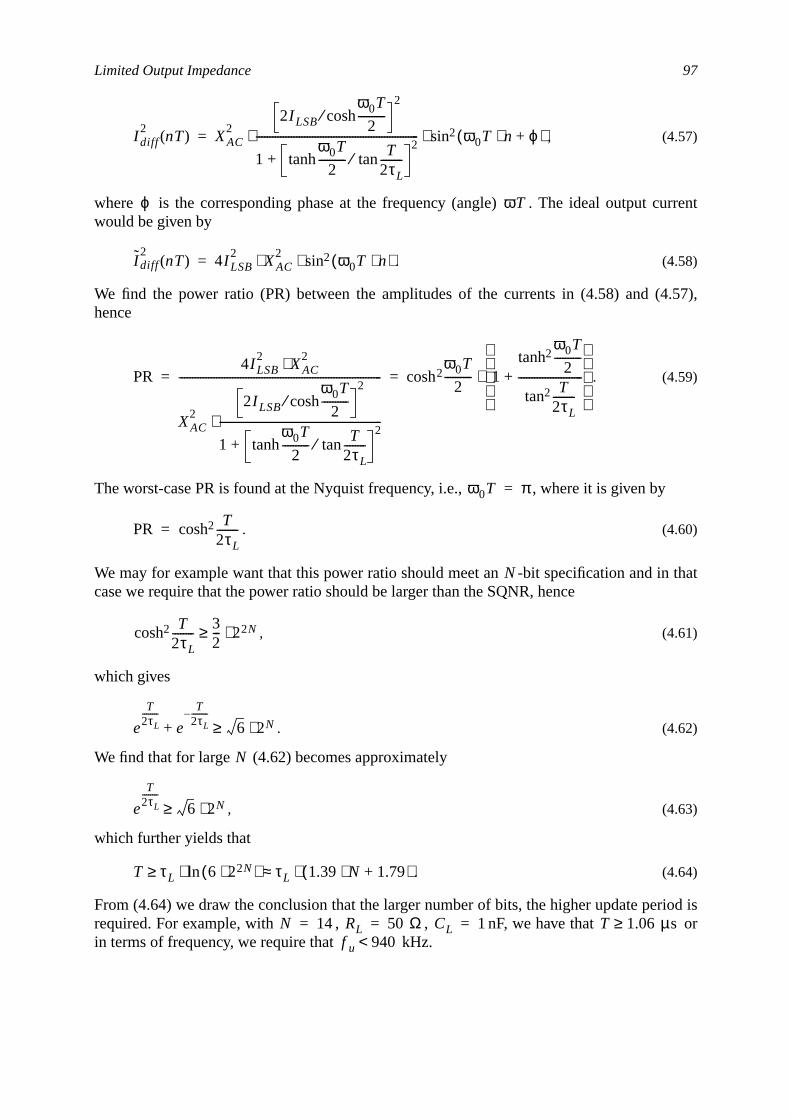
Limited Output Impedance 97
urrent
.57),
that
iod isor
, (4.57)
where is the corresponding phase at the frequency (angle) . The ideal output cwould be given by
. (4.58)
We find the power ratio (PR) between the amplitudes of the currents in (4.58) and (4hence
. (4.59)
The worst-case PR is found at the Nyquist frequency, i.e., , where it is given by
. (4.60)
We may for example want that this power ratio should meet an -bit specification and incase we require that the power ratio should be larger than the SQNR, hence
, (4.61)
which gives
. (4.62)
We find that for large (4.62) becomes approximately
, (4.63)
which further yields that
. (4.64)
From (4.64) we draw the conclusion that the larger number of bits, the higher update perrequired. For example, with , , nF, we have thatin terms of frequency, we require that kHz.
I diff2
nT( ) XAC2
2I LSB
ω0T
2----------cosh⁄
2
1ω0T
2----------tanh T
2τL--------tan⁄
2+
------------------------------------------------------------- ω0T n⋅ ϕ+( )sin2⋅ ⋅=
ϕ ωT
I diff2
nT( ) 4I LSB2
XAC2 ω0T n⋅( )sin2⋅ ⋅=
PR4I LSB
2XAC
2⋅
XAC2
2I LSB
ω0T
2----------cosh⁄
2
1ω0T
2----------tanh T
2τL--------tan⁄
2+
-------------------------------------------------------------⋅
---------------------------------------------------------------------------- cosh2ω0T
2---------- 1
ω0T
2----------tanh2
T2τL--------tan2
------------------------+
⋅= =
ω0T π=
PR T2τL--------cosh2=
N
T2τL--------cosh2
32--- 22N⋅≥
e
T2τL--------
e
T2τL--------–
+ 6 2N⋅≥
N
e
T2τL--------
6 2N⋅≥
T τL 6 22N⋅( )ln⋅ τL 1.39 N⋅ 1.79+( )⋅≈≥
N 14= RL 50 Ω= CL 1= T 1.06 µs≥f u 940<
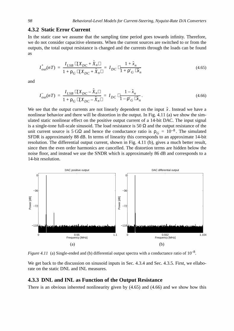
98 Behavioral-Level Models for Current-Steering, Nyquist-Rate D/A Converters
efore,m the
e found
have asim-gnaleted4-bitsult,ow thes to a
llabo-
this
4.3.2 Static Error CurrentIn the static case we assume that the sampling time period goes towards infinity. Therwe do not consider capacitive elements. When the current sources are switched to or frooutputs, the total output resistance is changed and the currents through the loads can bas
(4.65)
and
. (4.66)
We see that the output currents are not linearly dependent on the input . Instead wenonlinear behavior and there will be distortion in the output. In Fig. 4.11 (a) we show theulated static nonlinear effect on the positive output current of a 14-bit DAC. The input siis a single-tone full-scale sinusoid. The load resistance is 50Ω and the output resistance of thunit current source is 5 GΩ and hence the conductance ratio is . The simulaSFDR is approximately 88 dB. In terms of linearity this corresponds to an approximate 1resolution. The differential output current, shown in Fig. 4.11 (b), gives a much better resince then the even order harmonics are cancelled. The distortion terms are hidden belnoise floor, and instead we use the SNDR which is approximately 86 dB and correspond14-bit resolution.
We get back to the discussion on sinusoid inputs in Sec. 4.3.4 and Sec. 4.3.5. First, we erate on the static DNL and INL measures.
4.3.3 DNL and INL as Function of the Output ResistanceThere is an obvious inhereted nonlinearity given by (4.65) and (4.66) and we show how
(a) (b)
Figure 4.11 (a) Single-ended and (b) differential output spectra with a conductance ratio of 10–8.
I out+
nT( )I LSB XDC Xn+( )⋅
1 ρG XDC Xn+( )⋅+------------------------------------------------- I DC
1 xn+
1 ρ'G xn⋅+---------------------------⋅= =
I out–
nT( )I LSB XDC Xn–( )⋅
1 ρG XDC Xn–( )⋅+------------------------------------------------- I DC
1 xn–
1 ρ'G xn⋅–--------------------------⋅= =
x
ρG 10 8–=
0 0.55 1.1
−118
−72
−36
0
DAC positive output
Frequency [MHz]
Pow
er [d
B]
0 0.552 1.104
−118
−72
−36
0
DAC differential output
Frequency [MHz]
Pow
er [d
B]
Limited Output Impedance 99
nd,
valuese posi-
t sinceforthe
L isresis-
h aand
were
d thethe
affects the differential and integral nonlinearities (DNL and INL). The definitions of DNL aINL were given in Chapter 2 and for a ramped offset-binary input,
, they apply as
LSB (4.67)
and
LSB. (4.68)
In the static case (Sec. 4.3.2) we do not consider the capacitive elements and the settledare used. No best-fit line compensation has been applied to the definitions above. For thtive output current we find the DNL by inserting (4.65) in (4.67) and (4.68)
(4.69)
and
. (4.70)
The best-fit line can of course be derived as a function of the conductance parameter, buthe DNL and INL are of minor interest for our applications we leave this as a remarkfuture work. We find in (4.69) that the DNL is a decreasing monotonic function, sinceterm
(4.71)
is positive and decreasing towards zero for increasing . This implies that DNalways larger than -1 LSB and less than 0 LSB. Therefore, with respect to finite outputtance the DAC is always monotonic.
In Fig. 4.12 we illustrate the DNL and INL for the single-ended output of a 14-bit DAC witconductance ratio of as the case in Sec. 4.3.2. In the figure we show the DNLINL associated with the best-fit line approach. The best-fit offset and gradient valuesfound to be approximately
and . (4.72)
Same DAC that was used for the simulation result shown in Fig. 4.11 (a) were used to finINL and DNL as plotted in Fig. 4.12. We identify the nonlinearity parameter fromassumption that the output current can be written
, (4.73)
X k=k 0 … 2N 1–, ,=
DNLk
I out k( ) I out k 1–( )–
I LSB---------------------------------------------- 1–=
INL k INL 0 DNL ii 1=
k
∑+I out k( ) I out 0( )–
I LSB------------------------------------- k–= =
DNLkk
1 ρG k⋅+----------------------- k 1–
1 ρG k 1–( )⋅+-------------------------------------– 1–= =
11 ρG k⋅+( ) 1 ρG k 1–( )⋅+( )⋅
-------------------------------------------------------------------------- 1– 11 ρG k⋅+( )2
------------------------------ 1–≈=
INL kk
1 ρG k⋅+----------------------- 0– k–
ρG k2⋅1 ρG k⋅+-----------------------–= =
11 ρG k⋅+( )2
------------------------------
X k=
ρG 10 8–=
I LSB 0.999836⋅ I LSB 0.447223⋅
c
I out a b X⋅ c X2⋅ O X( )+ + +=
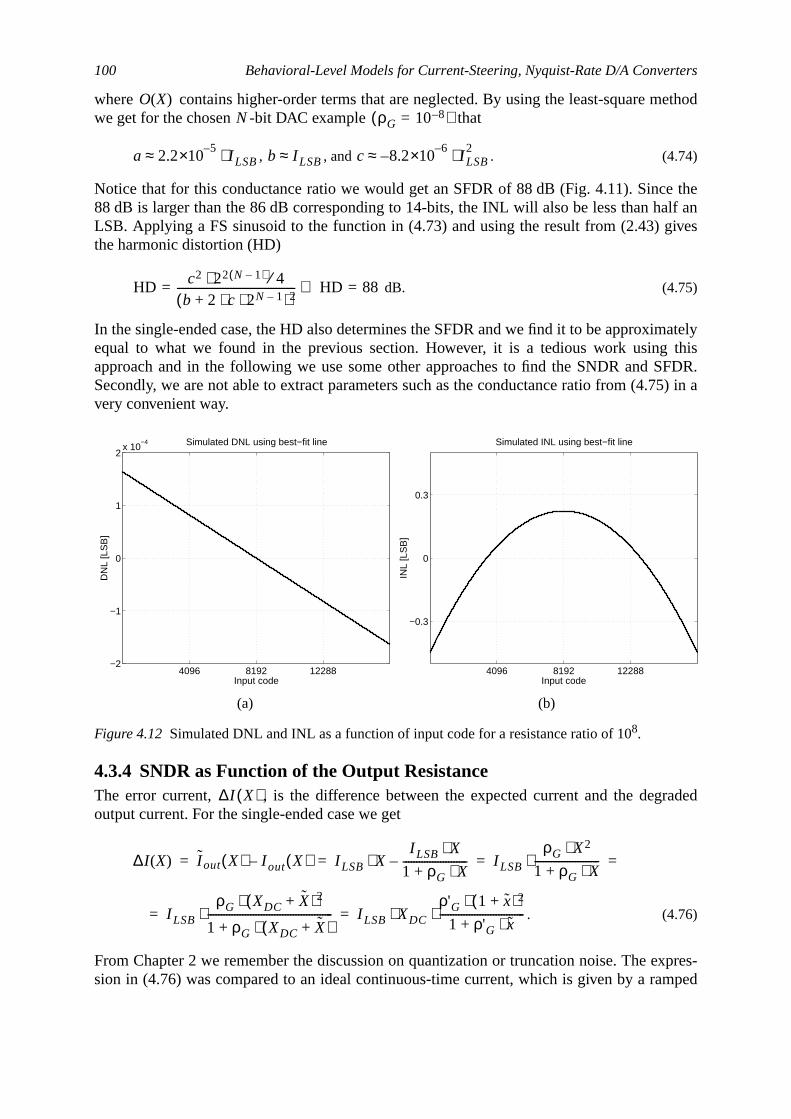
100 Behavioral-Level Models for Current-Steering, Nyquist-Rate D/A Converters
ethod
thelf anives
atelythisFDR.5) in a
raded
xpres-mped
where contains higher-order terms that are neglected. By using the least-square mwe get for the chosen -bit DAC example that
, , and . (4.74)
Notice that for this conductance ratio we would get an SFDR of 88 dB (Fig. 4.11). Since88 dB is larger than the 86 dB corresponding to 14-bits, the INL will also be less than haLSB. Applying a FS sinusoid to the function in (4.73) and using the result from (2.43) gthe harmonic distortion (HD)
dB. (4.75)
In the single-ended case, the HD also determines the SFDR and we find it to be approximequal to what we found in the previous section. However, it is a tedious work usingapproach and in the following we use some other approaches to find the SNDR and SSecondly, we are not able to extract parameters such as the conductance ratio from (4.7very convenient way.
4.3.4 SNDR as Function of the Output ResistanceThe error current, , is the difference between the expected current and the degoutput current. For the single-ended case we get
. (4.76)
From Chapter 2 we remember the discussion on quantization or truncation noise. The esion in (4.76) was compared to an ideal continuous-time current, which is given by a ra
(a) (b)
Figure 4.12 Simulated DNL and INL as a function of input code for a resistance ratio of 108.
O X( )N ρG 10 8–=( )
a 2.25–×10 I LSB⋅≈ b ILSB≈ c 8.2
6–×10– I LSB2⋅≈
HD c2 22 N 1–( )⋅ 4⁄b 2 c 2N 1–⋅ ⋅+( )2
--------------------------------------------= HD 88=⇒
4096 8192 12288−2
−1
0
1
2x 10
−4 Simulated DNL using best−fit line
Input code
DN
L [L
SB
]
4096 8192 12288
−0.3
0
0.3
Simulated INL using best−fit line
Input code
INL
[LS
B]
∆I X( )
∆I X( ) I out X( ) I out X( )– I LSB X⋅I LSB X⋅
1 ρG X⋅+------------------------– I LSB
ρG X2⋅1 ρG X⋅+------------------------⋅= = = =
I LSB
ρG XDC X+( )2⋅
1 ρG XDC X+( )⋅+-----------------------------------------------⋅ I LSB XDC
ρ'G 1 x+( )2⋅1 ρ'G x⋅+
--------------------------------⋅ ⋅= =

Limited Output Impedance 101
rrenton the
con-
theizationf the
well.ot easy
nce
input. The error power, , is given by the difference between the continuous-time cuand the piece-wise linear output current and hence the error power is also dependentcode applied to the converter
, (4.77)
where is the update period. From (4.77) we identify the quantization noise power
. (4.78)
We find the time-average error power (the expected output power) to be
, (4.79)
where is the time-averaged power of the error current introduced by the degradedverter is denoted
. (4.80)
Let the input signal be a sinusoid
, (4.81)
where is the DC level of the signal, is the amplitude of the sinusoid, isnormalized angular frequency, is the sequence index, and corresponds to the quanterror which is considered to be white for higher-resolution converters. The AC power osinusoid at the output is given by
. (4.82)
Due to the nonlinearity, there will be distortion terms folded back onto the signal tone asThe extraction of an exact formula can become somewhat tedious and the results are nto interpret (Sec. 8.3). Therefore, an approximate of the average error, , is used as
, (4.83)
where . Further on, we neglect the DC error, since this is of less importafor us. Therefore, we get
Pe
Pe X( )1T--- ∆I X( )
tT--- I LSB⋅
–2
td
T 2⁄–
T 2⁄
∫I LSB
2–
3------------- ∆I X( )
I LSB-------------- t
T---–
3
T 2⁄–
T 2⁄⋅= = =
I LSB2
12---------- ∆I X( )[ ]2+=
T
Pq
I LSB2
12----------=
Pe X( ) Pe Pq Pε+= =
Pε
Pε ∆I X( )[ ]2=
X n( ) XDC XAC ωT n⋅( )sin⋅ ν+ +=
XDC XAC ωTn ν
Ps
XAC2
2---------- I LSB
2⋅=
Pε
Pε I LSB XDC
ρ'G 1 x+( )2⋅1 ρ'G x⋅+
--------------------------------⋅ ⋅2
I LSB XDC ρ'G 1 x+( )2⋅⋅ ⋅[ ]2≈= =
I LSB XDC ρ'G⋅ ⋅( )2 1 x+( )4⋅ I LSB XDC ρ'G⋅ ⋅( )2 162---x2 3
8---x4+ +
⋅= =
x XAC XDC⁄=
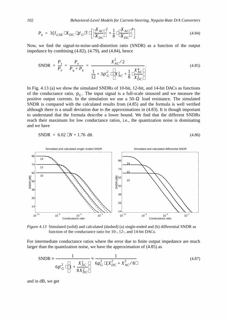
102 Behavioral-Level Models for Current-Steering, Nyquist-Rate D/A Converters
tput
ionse thelatedifiedrtantDRsating
much
as
(4.84)
Now, we find the signal-to-noise-and-distortion ratio (SNDR) as a function of the ouimpedance by combining (4.82), (4.79), and (4.84), hence
. (4.85)
In Fig. 4.13 (a) we show the simulated SNDRs of 10-bit, 12-bit, and 14-bit DACs as functof the conductance ratio, . The input signal is a full-scale sinusoid and we measurpositive output currents. In the simulation we use a 50- load resistance. The simuSNDR is compared with the calculated results from (4.85) and the formula is well veralthough there is a small deviation due to the approximations in (4.83). It is though impoto understand that the formula describe a lower bound. We find that the different SNreach their maximum for low conductance ratios, i.e., the quantization noise is dominand we have
dB. (4.86)
For intermediate conductance ratios where the error due to finite output impedance arelarger than the quantization noise, we have the approximation of (4.85) as
(4.87)
and in dB, we get
Figure 4.13 Simulated (solid) and calculated (dashed) (a) single-ended and (b) differential SNDRfunction of the conductance ratio for 10-, 12-, and 14-bit DACs.
Pε 3 I LSB XDC ρ'G⋅ ⋅( )2XAC
XDC----------
2 18---
XAC
XDC----------
4⋅+⋅=
SNDRPs
Pe-----
Ps
Pq Pε+------------------
XAC2
2⁄
112------ 3ρ'G
2XAC
2 18---
XAC4
XDC2
-----------⋅+
⋅+
----------------------------------------------------------------------= = =
ρGΩ
SNDR 6.02 N⋅ 1.76+=
10−10
10−8
10−6
10−4
14
26
38
50
62
74
8614
12
10
Simulated and calculated single−ended SNDR
SN
DR
[dB
]
Conductance ratio10
−1010
−810
−610
−414
26
38
50
62
74
8614
12
10
Simulated and calculated differential SNDR
SN
DR
[dB
]
Conductance ratio
SNDR1
6ρ'G2
1XAC
2
8XDC2
--------------+
⋅
--------------------------------------------- 1
6ρG2
XDC2
XAC2
8⁄+( )⋅------------------------------------------------------≈ ≈
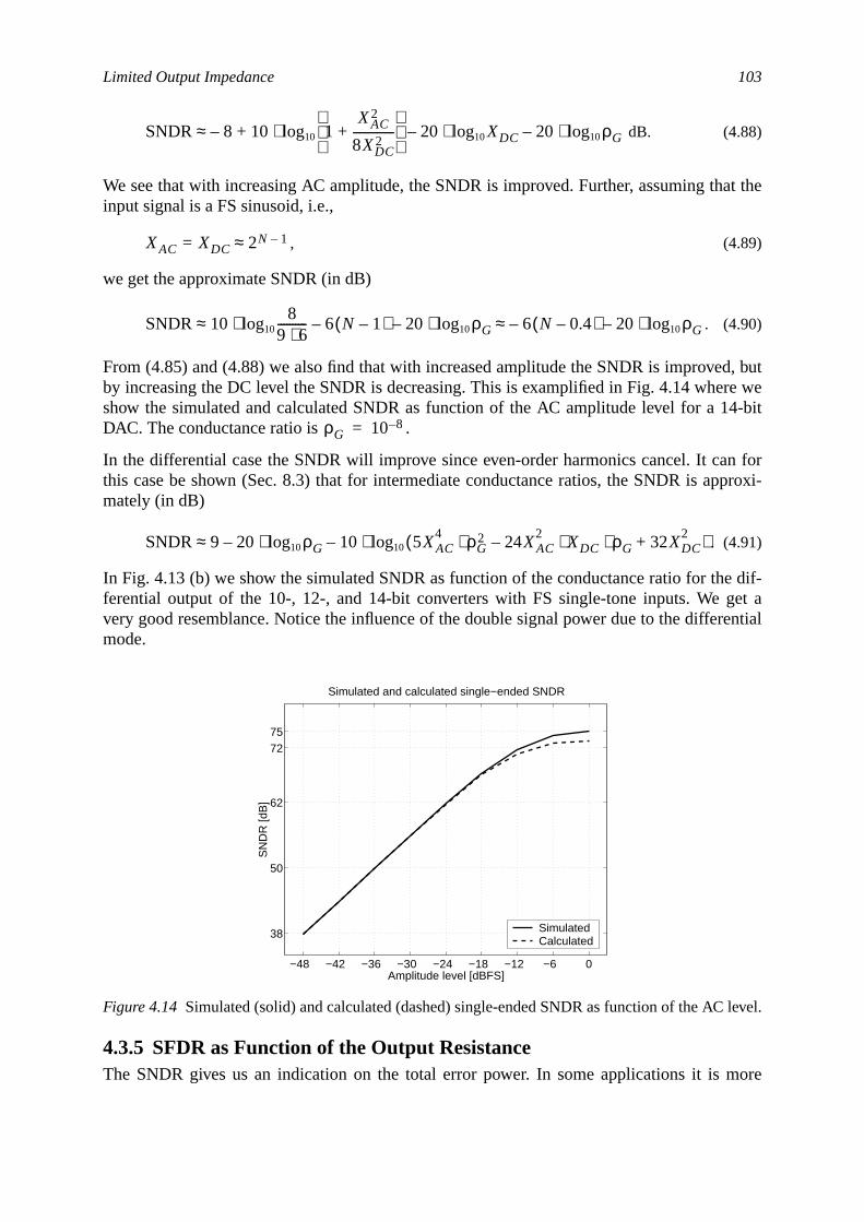
Limited Output Impedance 103
at the
, bute we4-bit
n forproxi-
dif-et a
ential
ore
level.
dB. (4.88)
We see that with increasing AC amplitude, the SNDR is improved. Further, assuming thinput signal is a FS sinusoid, i.e.,
, (4.89)
we get the approximate SNDR (in dB)
. (4.90)
From (4.85) and (4.88) we also find that with increased amplitude the SNDR is improvedby increasing the DC level the SNDR is decreasing. This is examplified in Fig. 4.14 whershow the simulated and calculated SNDR as function of the AC amplitude level for a 1DAC. The conductance ratio is .
In the differential case the SNDR will improve since even-order harmonics cancel. It cathis case be shown (Sec. 8.3) that for intermediate conductance ratios, the SNDR is apmately (in dB)
. (4.91)
In Fig. 4.13 (b) we show the simulated SNDR as function of the conductance ratio for theferential output of the 10-, 12-, and 14-bit converters with FS single-tone inputs. We gvery good resemblance. Notice the influence of the double signal power due to the differmode.
4.3.5 SFDR as Function of the Output ResistanceThe SNDR gives us an indication on the total error power. In some applications it is m
Figure 4.14 Simulated (solid) and calculated (dashed) single-ended SNDR as function of the AC
SNDR 8– 10 1XAC
2
8XDC2
--------------+
log10⋅ 20 XDClog10⋅– 20 ρGlog10⋅–+≈
XAC XDC= 2N 1–≈
SNDR 108
9 6⋅----------log10⋅ 6 N 1–( )– 20 ρGlog10⋅– 6 N 0.4–( )– 20 ρGlog10⋅–≈ ≈
ρG 10 8–=
SNDR 9 20 ρGlog10⋅– 10 5XAC4 ρG
2⋅ 24XAC2
XDC ρG⋅⋅– 32XDC2
+( )log10⋅–≈
−48 −42 −36 −30 −24 −18 −12 −6 0
38
50
62
7275
Simulated and calculated single−ended SNDR
SN
DR
[dB
]
Amplitude level [dBFS]
Simulated Calculated
104 Behavioral-Level Models for Current-Steering, Nyquist-Rate D/A Converters
spe-on ofusoid
the
r thisn wetone.iden-
nd
itten
e and
ono-
interesting to find out how the error is distributed throughout the frequency domain. Ecially, how large the harmonics are. They can be derived by finding the Taylor expansithe transfer characteristics. We may also find them by considering the case of single sininput as given in (4.81). The current through the load as determined by (4.65) becomes
, (4.92)
where and the noise term from (4.81) has been neglected. To simplifynotation, we let be the angle. (4.92) is rewritten as
. (4.93)
Examining (4.93) we find that only the second term contains AC components, hence foanalysis we neglect the first DC term. When finding the SFDR or the harmonic distortioonly care about the power ratio between the fundamental and the largest harmonicTherefore, the sign and the gain factor of the second term may be neglected as well. Wetify a normalized AC current as
, (4.94)
where
. (4.95)
We assume that the signal is not clipping which normally implies that a. Therefore, we also know that
(4.96)
and
. (4.97)
Using the property in (4.97) we know that the normalized AC current in (4.94) can be wras a converging Taylor expansion series. We have
. (4.98)
We isolate the DC term and the fundamental tone and we split the sum into the positivnegative values
(4.99)
The DC level (unity) and the linear gain can once again be neglected. By using trig
I out X( )I LSB XDC XAC αsin⋅+( )⋅
1 ρG XDC XAC αsin⋅+( )⋅+--------------------------------------------------------------------- I DC
1 x αsin⋅+1 ρ'G x αsin⋅⋅+----------------------------------------⋅= =
x XAC XDC⁄= να ωT n⋅=
I out X( ) I DC 1 1ρ'G-------+
⋅I DC
ρ'G--------- 1
1 ρ'G x αsin⋅ ⋅+----------------------------------------⋅–=
I AC X( ) 11 ρ'G x αsin⋅ ⋅+---------------------------------------- 1
1 A αsin⋅+-----------------------------= =
A ρ'G x⋅ ρ'GXAC
XDC----------⋅
ρG XAC⋅1 ρG XDC⋅+-------------------------------= = =
XAC XDC<XDC 2N 1–≈
0 A 1<≤
A αsin⋅ 1<
I AC X( ) A–( )n αsinn⋅n 0=
∞
∑=
I AC X( ) 1 A αsin⋅– A2n αsin2n⋅n 1=
∞
∑ A2n 1+ αsin2n 1+⋅n 1=
∞
∑–+=
A( )
Limited Output Impedance 105
e thehar-
r ratio
itude
e that
e seescale
metric formulas, we find that (4.98) is equal to
,
(4.100)
where contains the DC component and higher order harmonics that do not influencSFDR. In Sec. 8.3 a derivation of the SFDR is given and it is shown that the power of themonics are decreasing with higher frequencies. The SFDR is now found as the powebetween the fundamental and the second harmonic as
o. (4.101)
By substituting back from (4.95) in (4.101) we get the SFDR expressed in the ampllevels as
. (4.102)
When the conductance ratio, , is small, i.e., well-designed current sources, we hav(4.102) can be approximated
. (4.103)
Further, if , or , the SFDR becomes approximately
. (4.104)
In dB we may write (4.104) as
dB. (4.105)
The SFDR is strongly dependent on both the conductance ratio and the AC amplitude. Wthat for increasing AC amplitude, the SFDR decreases. For the (worst-) case of a full-signal, i.e. , we have
, (4.106)
which equals
I AC X( ) f X( ) αsin A 1A2---
2n 2n 1+n
n 1=
∞
∑+⋅ ⋅– 2αcos 2A2---
2n 2nn 1–
n 1=
∞
∑⋅–=
f X( )
SFDRA2
4------
1A2---
2n 2n 1+n
n 1=
∞
∑+
A2---
2n 2nn 1–
n 1=
∞
∑--------------------------------------------------------
2
⋅ 1 1 A2–+A
-----------------------------
2
= =
A
SFDR 1ρ'G x⋅--------------- 1
ρ'G x⋅( )2---------------------- 1–+
2=
ρG
SFDR 21
ρ'G x⋅---------------⋅
2≈ 4
ρ'G x⋅( )2----------------------=
ρG XDC⋅ 1« ρ'G ρG XDC⋅≈
SFDR4
ρG XAC⋅( )2-----------------------------≈
SFDR 104
ρG XAC⋅( )2-----------------------------log10⋅ 6 20 ρGlog10⋅– 20 XAClog10⋅–= =
XAC XDC= 2N 1–≈
SFDR 11
ρG XDC⋅---------------------- 1 1 2 XDC ρG⋅ ⋅++( )⋅+
2=
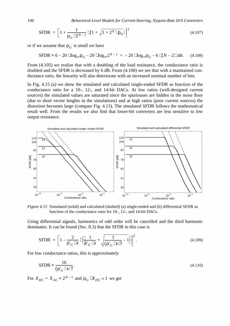
106 Behavioral-Level Models for Current-Steering, Nyquist-Rate D/A Converters
tio isd con-s.
of therentse floors) theatical
low
onic
as
(4.107)
or if we assume that is small we have
dB. (4.108)
From (4.105) we realize that with a doubling of the load resistance, the conductance radoubled and the SFDR is decreased by 6 dB. From (4.108) we see that with a maintaineductance ratio, the linearity will also deteriorate with an increased nominal number of bit
In Fig. 4.15 (a) we show the simulated and calculated single-ended SFDR as functionconductance ratio for a 10-, 12-, and 14-bit DACs. At low ratios (well-designed cursources) the simulated values are saturated since the spuriouses are hidden in the noi(due to short vector lenghts in the simulations) and at high ratios (poor current sourcedistortion becomes large (compare Fig. 4.13). The simulated SFDR follows the mathemresult well. From the results we also find that lower-bit converters are less sensitive tooutput resistance.
Using differential signals, harmonics of odd order will be cancelled and the third harmdominates. It can be found (Sec. 8.3) that the SFDR in this case is
. (4.109)
For low conductance ratios, this is approximately
. (4.110)
For and we get
Figure 4.15 Simulated (solid) and calculated (dashed) (a) single-ended and (b) differential SFDRfunction of the conductance ratio for 10-, 12-, and 14-bit DACs.
SFDR 11
ρG 2N 1–⋅------------------------ 1 1 2N ρG⋅++( )⋅+
2=
ρG
SFDR 6 20 ρGlog10⋅– 20 2N 1–log10⋅–≈ 20 ρGlog10⋅– 6 N 2–( )⋅–=
10−10
10−8
10−6
10−4
33
47
62
76
91
104110 14
12
10
Simulated and calculated single−ended SFDR
SF
DR
[dB
]
Conductance ratio10
−1010
−810
−610
−4
33
47
62
76
91
104110 14
12
10
Simulated and calculated differential SFDR
SF
DR
[dB
]
Conductance ratio
SFDR 12
ρ'G x⋅--------------- 1
ρ'G x⋅--------------- 1
ρ'G x⋅( )2---------------------- 1–+
⋅–2
=
SFDR16
ρ'G x⋅( )4----------------------≈
XDC XAC= 2N 1–≈ ρG XDC⋅ 1«
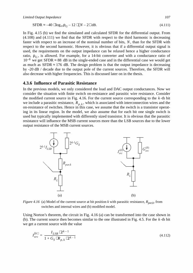
Limited Output Impedance 107
romasingwithal isuctanceio of
getasingR will
w wensiderth bitd the
operat-ch issiticlower
wn inth bit
dB. (4.111)
In Fig. 4.15 (b) we find the simulated and calculated SFDR for the differential output. F(4.108) and (4.111) we find that the SFDR with respect to the third harmonic is decrefaster with respect to an increase of the nominal number of bits, , than for the SFDRrespect to the second harmonic. However, it is obvious that if a differential output signused, the requirements on the output impedance can be relaxed hence a higher condratio, , is allowed. For example, for a 14-bit converter and with a conductance rat
we get dB in the single-ended case and in the differential case we wouldas much as dB. The design problem is that the output impedance is decreby -20 dB / decade due to the output pole of the current sources. Therefore, the SFDalso decrease with higher frequencies. This is discussed later on in the thesis.
4.3.6 Influence of Parasitic ResistanceIn the previous models, we only considered the load and DAC output conductances. Noconsider the situation with finite switch on-resistance and parasitic wire resistance. Cothe modified current source in Fig. 4.16. For the current source corresponding to the -we include a parasitic resistance, , which is associated with interconnection wires anon-resistance of switches. Hence in this case, we assume that the switch is a transistoring in its linear region. In the model, we also assume that for each bit one single switused but typically implemented with differently sized transistor. It is obvious that the pararesistance will influence the MSB current sources more than the LSB sources due to theoutput resistance of the MSB current sources.
Using Norton’s theorem, the circuit in Fig. 4.16 (a) can be transformed into the case sho(b). The current source then becomes similar to the one illustrated in Fig. 4.5. For the -we get a current source with the value
(4.112)
(a) (b)
Figure 4.16 (a) Model of the current source at bit positionk with parasitic resistance,Rpar,k, fromswitches and internal wires and (b) modified model.
SFDR 40– ρGlog10⋅ 12 N 2–( )⋅–≈
N
ρG10 8– SFDR 88≈
SFDR 176≈
kRp k,
2k-1GS2k-1ILSB
Rpar,k
RL
Isrc
RL
(k) Gsrc(k)
k
I srck( ) I LSB 2k 1–⋅
1 GS Rp k, 2k 1–⋅ ⋅+------------------------------------------------=
108 Behavioral-Level Models for Current-Steering, Nyquist-Rate D/A Converters
ession
gres-i.e.,
di-
DRfluence
fre-e inter-s that
withnal’squen-sed intrans-k fre-esultse used
and the output conductance
. (4.113)
The effects of the parasitics, as given in (4.112) and (4.113), can be included in the exprfor the output current as in (4.65)
, (4.114)
where are the individual bits in . If we assume that the switches are designed prosively so that the on-resistance is decreasing with higher bit significance,
. For this case, we have the output current from (4.114) as
. (4.115)
This will give rise to a gain error of and the conductance ratio will be mofied as
. (4.116)
The result from (4.116) is then be used in the expressions for DNL, INL, SFDR, and SNthat were derived in the previous sections. As the output conductance decreases, the inof the switch on-resistance becomes more severe.
4.3.7 SNDR and SFDR as Functions of the Output ImpedanceAs was illustrated in Fig. 4.9 and Fig. 4.10 we found that with higher signal and/or clockquencies the nonlinearity increases, hence the SNDR and SFDR decrease. It is thereforesting to know by how much these measures will decrease and which parameterdetermine the influence.
In Fig. 4.17 we show with solid lines how the measured differential SFDR is decreasinghigher sample frequency for a 14-bit DAC and two different input frequencies. The sigamplitude level is –3 dBFS. We see how the performance is decreasing with higher frecies and higher SUFR. The measured converter is a 5-V current-steering DAC proces0.6-µm CMOS and the output currents are terminated over 50 Ohms each and fed into aformer. We see that the SFDR is decreasing with higher SUFR and with increased clocquency by approximately –16 dB/decade. In the figure we show the simulated SFDR rwith dashed lines and same frequencies and amplitude levels. In the simulation, we hav
GSk( ) GS 2k 1–⋅
1 GS Rp k, 2k 1–⋅ ⋅+------------------------------------------------=
I out X( )
I srck( )
bk⋅k 1=
N
∑
1GS
k( )
GL---------- bk⋅
k 1=
N
∑+
----------------------------------------
I LSB
2k 1– bk⋅1 GS Rp k, 2k 1–⋅ ⋅+------------------------------------------------
k 1=
N
∑⋅
1 ρG
2k 1– bk⋅1 GS Rp k, 2k 1–⋅ ⋅+------------------------------------------------
k 1=
N
∑⋅+
-------------------------------------------------------------------------------= =
bk X
Rp k, 2 k 1–( )– Rp⋅=
I out X( )
I LSB
2k 1– bk⋅1 GS Rp⋅+---------------------------
k 1=
N
∑⋅
1 ρG
2k 1– bk⋅1 GS Rp⋅+---------------------------
k 1=
N
∑⋅+
----------------------------------------------------------
I LSB
1 GS Rp⋅+--------------------------- X⋅
1ρG
1 GS Rp⋅+--------------------------- X⋅+
---------------------------------------------= =
1 1 GS Rp⋅+( )⁄
ρG p,ρG
1 GS Rp⋅+---------------------------=
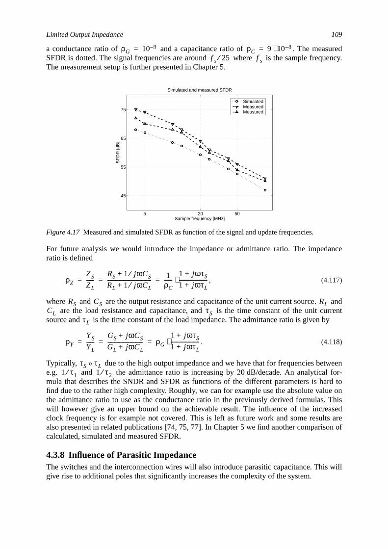
Limited Output Impedance 109
uredency.
ance
andurrent by
weenfor-
ard toue on. Thisaseds areon of
s will
a conductance ratio of and a capacitance ratio of . The measSFDR is dotted. The signal frequencies are around where is the sample frequThe measurement setup is further presented in Chapter 5.
For future analysis we would introduce the impedance or admittance ratio. The impedratio is defined
, (4.117)
where and are the output resistance and capacitance of the unit current source.are the load resistance and capacitance, and is the time constant of the unit c
source and is the time constant of the load impedance. The admittance ratio is given
. (4.118)
Typically, due to the high output impedance and we have that for frequencies bete.g. and the admittance ratio is increasing by 20 dB/decade. An analyticalmula that describes the SNDR and SFDR as functions of the different parameters is hfind due to the rather high complexity. Roughly, we can for example use the absolute valthe admittance ratio to use as the conductance ratio in the previously derived formulaswill however give an upper bound on the achievable result. The influence of the increclock frequency is for example not covered. This is left as future work and some resultalso presented in related publications [74, 75, 77]. In Chapter 5 we find another compariscalculated, simulated and measured SFDR.
4.3.8 Influence of Parasitic ImpedanceThe switches and the interconnection wires will also introduce parasitic capacitance. Thigive rise to additional poles that significantly increases the complexity of the system.
Figure 4.17 Measured and simulated SFDR as function of the signal and update frequencies.
ρG 10 9–= ρC 9 10 8–⋅=f s 25⁄ f s
5 20 50
45
55
65
75
Simulated and measured SFDR
Sample frequency [MHz]
SF
DR
[dB
]
SimulatedMeasured Measured
ρZ
ZS
ZL------
RS 1 jωCS⁄+
RL 1 jωCL⁄+----------------------------------
1ρC------
1 jωτS+
1 jωτL+----------------------⋅= = =
RS CS RLCL τS
τL
ρY
YS
YL------
GS jωCS+
GL jωCL+--------------------------- ρG
1 jωτS+
1 jωτL+----------------------⋅= = =
τS τL»1 τ1⁄ 1 τ2⁄
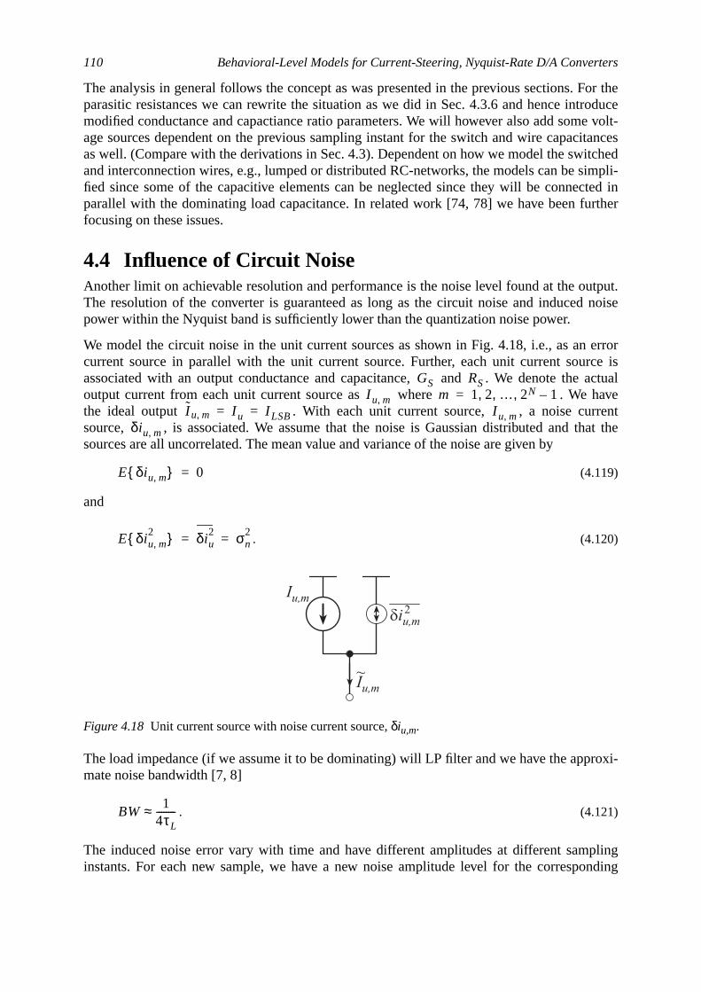
110 Behavioral-Level Models for Current-Steering, Nyquist-Rate D/A Converters
For theroducee volt-itancestchedimpli-ted inrther
tput.noise
errorrce isactualaveenthat the
roxi-
plingnding
The analysis in general follows the concept as was presented in the previous sections.parasitic resistances we can rewrite the situation as we did in Sec. 4.3.6 and hence intmodified conductance and capactiance ratio parameters. We will however also add somage sources dependent on the previous sampling instant for the switch and wire capacas well. (Compare with the derivations in Sec. 4.3). Dependent on how we model the swiand interconnection wires, e.g., lumped or distributed RC-networks, the models can be sfied since some of the capacitive elements can be neglected since they will be connecparallel with the dominating load capacitance. In related work [74, 78] we have been fufocusing on these issues.
4.4 Influence of Circuit NoiseAnother limit on achievable resolution and performance is the noise level found at the ouThe resolution of the converter is guaranteed as long as the circuit noise and inducedpower within the Nyquist band is sufficiently lower than the quantization noise power.
We model the circuit noise in the unit current sources as shown in Fig. 4.18, i.e., as ancurrent source in parallel with the unit current source. Further, each unit current souassociated with an output conductance and capacitance, and . We denote theoutput current from each unit current source as where . We hthe ideal output . With each unit current source, , a noise currsource, , is associated. We assume that the noise is Gaussian distributed and tsources are all uncorrelated. The mean value and variance of the noise are given by
(4.119)
and
. (4.120)
The load impedance (if we assume it to be dominating) will LP filter and we have the appmate noise bandwidth [7, 8]
. (4.121)
The induced noise error vary with time and have different amplitudes at different saminstants. For each new sample, we have a new noise amplitude level for the correspo
Figure 4.18 Unit current source with noise current source,δiu,m.
GS RSI u m, m 1 2 … 2N 1–, , ,=
I u m, I u I LSB= = I u m,δiu m,
E δiu m, 0=
E δiu m,2 δiu
2 σn2
= =
Iu,m
diu,m2
Iu,m~
BW1
4τL--------≈
Influence of Circuit Noise 111
dent of
set ofutput
ionave
utputwenction
omi-ds ofre-
r a
rcend by
current sources. We assume that the standard deviation and mean values are indepentime. We have the output current with the noise included (at the sampling instants)
, (4.122)
where is the set of unit current sources associated with the -th bit. Typically, thesetransistors is chosen so that the matching errors are minimized. The normalized total onoise power, , within the bandwidth, , is given by the sum of the contributfrom all noise sources, and the instantenous sum is signal and time dependent [7]. We h
. (4.123)
According to the discussions in the previous section, the noise current directed to the owill in reality be influenced by the limited output impedance of the current source [7]. Ifassume that the internal capacitance do not influence the result, we have a transfer fufrom each noise current source to the output as
. (4.124)
If we assume that the output resistance is very high, i.e., , we get that the pole dnates further yielding the noise bandwidth as described in (4.121). Including these kinnonidealities will only introduce minor modifications to the following derivations and thefore we neglect their influence. We have the time-averaged normalized noise power
, (4.125)
where is the input DC level which normally is set to . The output power fosinusoid is given by
, (4.126)
where is the AC amplitude and is the nominal output current of the LSB souwhich in most designs corresponds to the unit current source size, . The SNR is foucomparing (4.125) with (4.126) and adding the quantization noise as we did in (4.76)
I out nTs( ) I u X nT( )⋅ bk nT( ) δiu m, nT( )m Mk∈∑⋅
k 1=
N
∑+=
Mk k
Pn nT( ) BW
Pn nT( ) δi tot2
E bk nT( ) δiu m, nT( )m Mk∈∑⋅
k 1=
N
∑2
= = =
bk2
nT( ) E δiu m,2
nT( ) m Mk∈∑⋅
k 1=
N
∑ bk nT( ) σn2
m Mk∈∑⋅
k 1=
N
∑= = =
σn2
bk nT( ) 2k 1–⋅k 1=
N
∑⋅ σn2
X nT( )⋅= =
H s( )GL
GL sCL GS sCS+ + +---------------------------------------------------- 1
1 ρG s τL τS ρG⋅+( )+ +----------------------------------------------------------= =
ρG 0≈
Pn Pn nT( ) σn2
X nT( )⋅ σn2
XDC⋅= = =
XDC FS 2⁄
Ps
XAC2
2---------- I LSB
2⋅=
XAC I LSBI u
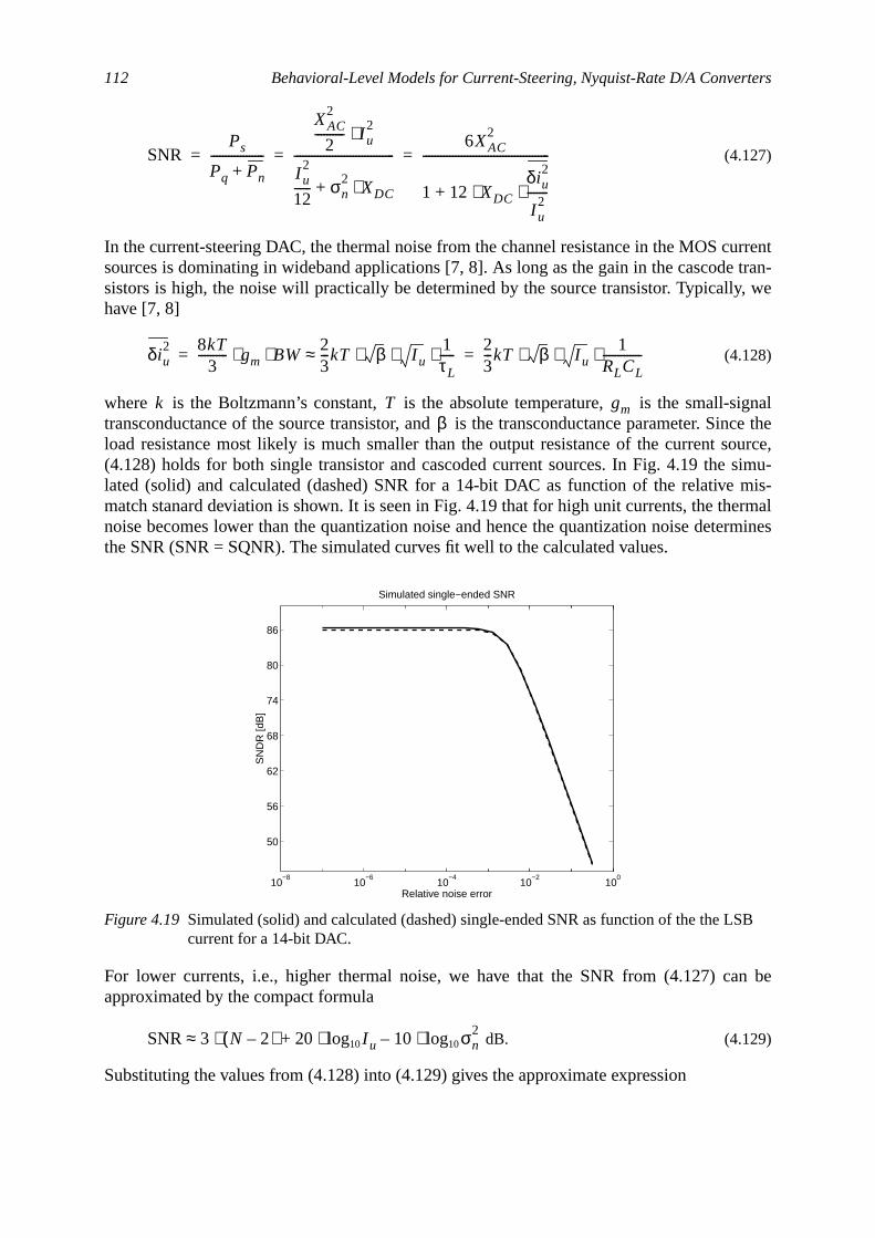
112 Behavioral-Level Models for Current-Steering, Nyquist-Rate D/A Converters
urrenttran-
, we
ignalince theource,simu-mis-ermalrmines
n be
SB
(4.127)
In the current-steering DAC, the thermal noise from the channel resistance in the MOS csources is dominating in wideband applications [7, 8]. As long as the gain in the cascodesistors is high, the noise will practically be determined by the source transistor. Typicallyhave [7, 8]
(4.128)
where is the Boltzmann’s constant, is the absolute temperature, is the small-stransconductance of the source transistor, and is the transconductance parameter. Sload resistance most likely is much smaller than the output resistance of the current s(4.128) holds for both single transistor and cascoded current sources. In Fig. 4.19 thelated (solid) and calculated (dashed) SNR for a 14-bit DAC as function of the relativematch stanard deviation is shown. It is seen in Fig. 4.19 that for high unit currents, the thnoise becomes lower than the quantization noise and hence the quantization noise detethe SNR (SNR = SQNR). The simulated curves fit well to the calculated values.
For lower currents, i.e., higher thermal noise, we have that the SNR from (4.127) caapproximated by the compact formula
dB. (4.129)
Substituting the values from (4.128) into (4.129) gives the approximate expression
Figure 4.19 Simulated (solid) and calculated (dashed) single-ended SNR as function of the the Lcurrent for a 14-bit DAC.
SNRPs
Pq Pn+------------------
XAC2
2---------- I u
2⋅
I u2
12------ σn
2XDC⋅+
----------------------------------6XAC
2
1 12 XDC
δiu2
I u2
-------⋅ ⋅+
-------------------------------------------= = =
δiu2 8kT
3---------- gm BW⋅ ⋅ 2
3---kT β I u
1τL-----⋅ ⋅ ⋅≈ 2
3---kT β I u
1RLCL-------------⋅ ⋅ ⋅= =
k T gmβ
10−8
10−6
10−4
10−2
100
50
56
62
68
74
80
86
Simulated single−ended SNR
SN
DR
[dB
]
Relative noise error
SNR 3 N 2–( )⋅ 20 I ulog10⋅ 10 σn2
log10⋅–+≈
Current Source Mismatch 113
. Forwith
i.e.,
aram-
ped-s the
ts wille cur-nals.
ed byfurther
dis-r cur-s theo notwithis dis-e, we
imilar. 4.20ed toourcet is
error,
dB. (4.130)
Now, we find how the choice of transistor sizes and unit current values influence the SNRexample, consider (4.129). For a 14-bit resolution, we must guarantee that the SNRrespect to the thermal nosie is higher than the quantization noise,
dB. Thereby, we have
dB. (4.131)
From (4.131) we get
. (4.132)
From this equation and (4.128), etc., we can then derive the necessary limits on design peters, such as the transistor widths, etc.
4.5 Current Source MismatchIn an actual implementation, the current sources will not only due to the limited output imance and circuit noise give a fault output current. The influence of matching errors makesizes of the transistors to differ from their designed values and hence the output currennot be correct. In fact, the matching errors tend to be the dominating error sources in thrent-steering DACs, since the matching errors are not cancelled by using differential sigFor the CMOS current source, the so called - and -mismatch can be characteriztheir distribution, the transistor sizes, and physical distance [68, 69]. These issues areaddressed in Chapter 5 and in this chapter we stay on a higher level of abstraction.
In a similar way as we have derived in the previous sections, the output signal will betorted. Since a matching error is associated with a certain bit and hence the output errorent will become signal-dependent. Unlike the noise current, which is of similar nature amatching error, the matching errors for one single DAC or chip are static. Hence, they dchange as function of time, signal or clock frequency. When comparing several chipseachother the matching errors will become Gaussian distributed. Therefore, the analyscussed in this section will focus on the case of comparing a large number of chips. Hencwant to find the expected SFDR and SNDR for a certain standard deviation.
A current source with mismatch error can be modeled as an additional current source (sto the noise current source) in parallel with the nominal current source, as shown in Figfor the -th LSB current source. We still assume that unit current sources are usdefine this current source. We denote the actual output current from each unit current sas where . Also in this case, we assume that the ideal outpu
. For each unit current source, we associate an absolute matching and hence the actual current becomes
. (4.133)
The relative matching error is given by
SNR 3 N 2–( )⋅ 15 I ulog10⋅ 5 βlog10⋅– 102kT 3⁄RLCL
-----------------log10⋅–+≈
SNR 6.02 N⋅ 1.76+≥
3 N 2–( )⋅ 20 I ulog10⋅ 10 σn2
log10⋅–+ 6.02 N⋅ 1.76+≥
σn2 I u
2
3 2N 1+⋅---------------------≤
β VT
k 2k 1–
I u m, m 1 2 … 2N 1–, , ,=I u m, I u I LSB= =δI u m,
I u m, I u m, δI u m,+ I u δI u m,+= =
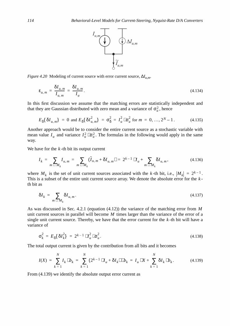
114 Behavioral-Level Models for Current-Steering, Nyquist-Rate D/A Converters
nt and
le withame
.the -
mr of ave a
. (4.134)
In this first discussion we assume that the matching errors are statistically independethat they are Gaussian distributed with zero mean and a variance of , hence
and for . (4.135)
Another approach would be to consider the entire current source as a stochastic variabmean value and variance . The formulas in the following would apply in the sway.
We have for the -th bit its output current
, (4.136)
where is the set of unit current sources associated with the -th bit, i.e.,This is a subset of the entire unit current source array. We denote the absolute error forth bit as
. (4.137)
As was discussed in Sec. 4.2.1 (equation (4.12)) the variance of the matching error frounit current sources in parallel will become times larger than the variance of the errosingle unit current source. Thereby, we have that the error current for the -th bit will havariance of
. (4.138)
The total output current is given by the contribution from all bits and it becomes
. (4.139)
From (4.139) we identify the absolute output error current as
Figure 4.20 Modeling of current source with error current source,∆Iu,m.
Iu,m
DIu,m
Iu,m~
εu m,δI u m,I u m,
-------------δI u m,
I u-------------= =
σu2
Eδ δI u m, 0= Eδ δI u m,2 σδ
2I u
2 σu2⋅= = m 0 … 2N 1–, ,=
I u I u2 σu
2⋅
k
I k I u m,m Mk∈∑ I u m, δI u m,+( )
m Mk∈∑ 2k 1– I u⋅ δI u m,
m Mk∈∑+= = =
Mk k Mk 2k 1–=k
δI k δI u m,m Mk∈∑=
MM
k
σk2
Eδ δI k2 2k 1– I u
2 σu2⋅ ⋅= =
I X( ) I k bk⋅k 1=
N
∑ 2k 1– I u⋅ δI k+( ) bk⋅k 1=
N
∑ I u X⋅ δI k bk⋅k 1=
N
∑+= = =
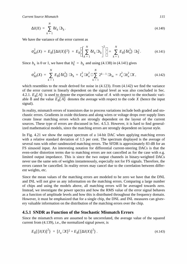
Current Source Mismatch 115
ianceSec.vari-input
d sto-linesrrentneral-tyle.
rorsge ofor anthe
th e.g.ACsre, the
differ-
e DNLberzero.haves
main.ivev-
squared
. (4.140)
We have the variance of the error current as
. (4.141)
Since is 0 or 1, we have that and using (4.138) in (4.141) gives
, (4.142)
which resembles to the result derived for noise in (4.123). From (4.142) we find the varof the error current is linearly dependent on the signal level as was also concluded in4.2.1. is used to denote the expectation value of with respect to the stochasticable and the value denotes the average with respect to the code (hence thesignal).
In reality, mismatch errors of transistors due to process variations include both graded anchastic errors. Gradients in oxide thickness and along wires or voltage drops over supplycreate linear matching errors which are strongly dependent on the layout of the cusources. These type of errors are discussed in Sec. 4.5.3. However, it is hard to find geized mathematical models, since the matching errors are strongly dependent on layout s
In Fig. 4.21 we show the output spectrum of a 14-bit DAC when applying matching erwith a relative standard deviation of 1.5 per cent. The spectrum displayed is the averaseveral runs with other randmozied matching errors. The SFDR is approximately 83 dB fFS sinusoid input. An interesting notation for differential current-steering DACs is thateven-order distortion terms due to matching errors are not cancelled as for the case wilimited output impedance. This is since the two output channels in binary-weighted Dnever use the same sets of weights instantenously, especially not for FS signals. Therefoerrors cannot be cancelled. In reality errors may cancel due to the correlation betweenent weights, etc.
Since the mean values of the matching errors are modeled to be zero we have that thand INL will not give us any information on the matching errors. Comparing a large numof chips and using the models above, all matching errors will be averaged towardsInstead, we investigate the power spectra and how the RMS value of the error signal beas a function of amplitude levels and how this is distributed throughout the frequency doHowever, it must be emphasized that for a single chip, the DNL and INL measures can gery valuable information on the distribution of the matching errors over the chip.
4.5.1 SNDR as Function of the Stochastic Mismatch ErrorsSince the mismatch errors are assumed to be uncorrelated, the average value of thecurrent from (4.139), i.e., the normalized signal power, is
. (4.143)
∆I X( ) δI k bk⋅k 1=
N
∑=
σ∆I2
X( ) Eδ ∆I X( )[ ]2 Eδ δI k bk⋅k 1=
N
∑2
Eδ δI k2 bk
2⋅k 1=
N
∑= = =
bk bk2 bk=
σ∆I2
X( ) Eδ δI k2 bk⋅
k 1=
N
∑ I u2 σu
2⋅ 2k 1– bm⋅k 1=
N
∑⋅ I u2 σu
2X⋅ ⋅= = =
Eδ A Aδ Eδ A X
Eδ I X( )[ ]2 I u X⋅[ ]2 Eδ ∆I X( )[ ]2 +=
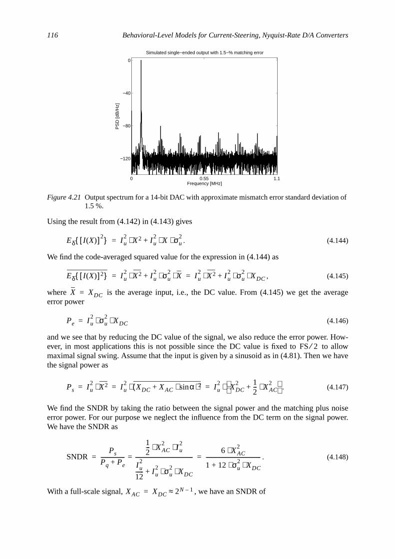
116 Behavioral-Level Models for Current-Steering, Nyquist-Rate D/A Converters
rage
How-llowhave
noiseower.
n of
Using the result from (4.142) in (4.143) gives
. (4.144)
We find the code-averaged squared value for the expression in (4.144) as
, (4.145)
where is the average input, i.e., the DC value. From (4.145) we get the aveerror power
(4.146)
and we see that by reducing the DC value of the signal, we also reduce the error power.ever, in most applications this is not possible since the DC value is fixed to to amaximal signal swing. Assume that the input is given by a sinusoid as in (4.81). Then wethe signal power as
. (4.147)
We find the SNDR by taking the ratio between the signal power and the matching pluserror power. For our purpose we neglect the influence from the DC term on the signal pWe have the SNDR as
. (4.148)
With a full-scale signal, , we have an SNDR of
Figure 4.21 Output spectrum for a 14-bit DAC with approximate mismatch error standard deviatio1.5 %.
0 0.55 1.1
−120
−80
−40
0
Simulated single−ended output with 1.5−% matching error
PS
D [d
B/H
z]
Frequency [MHz]
Eδ I X( )[ ]2 I u2
X2⋅ I u2
X σu2⋅ ⋅+=
Eδ I X( )[ ]2 I u2
X2⋅ I u2 σu
2X⋅⋅+ I u
2X2⋅ I u
2 σu2
XDC⋅⋅+= =
X XDC=
Pe I u2 σu
2XDC⋅⋅=
FS 2⁄
Ps I u2
X2⋅ I u2
XDC XAC αsin⋅+( )2⋅ I u2
XDC2 1
2--- XAC
2⋅+ ⋅= = =
SNDRPs
Pq Pe+------------------
12--- XAC
2I u
2⋅ ⋅
I u2
12------ I u
2 σu2
XDC⋅ ⋅+
-------------------------------------------=6 XAC
2⋅
1 12 σu2
XDC⋅ ⋅+-----------------------------------------= =
XAC XDC 2N 1–≈=
Current Source Mismatch 117
f theults
e findlated
n theFor
tes thes thes thecoeffi-
r stan-
. (4.149)
In dB we have that
dB. (4.150)
In Fig. 4.22 we show the simulated (solid) and calculated (dashed) SNDR as function omismatch for 10-, 12-, and 14-bit DACs. The input signal is full-scale. The simulation reswere found by taking the average value of 1024 simulations for each mismatch value. Wthat the simulated values match the calculated ones well. At low mismatch the simucurves reach their ideal values determined by dB.
4.5.2 SFDR as Function of the Stochastic Mismatch ErrorsTo find the SFDR, we have to investigate how the mismatch error power is distributed ifrequency domain. We will do this by investigating the Fourier series coefficients, .bit we have
, (4.151)
where is the sequence index, is the signal period in number of samples, and denofrequency, i.e., corresponds to the normalized angular frequency , etc. isignal angular frequency and is the sample period. Each Fourier coefficient stateamplitude and phase of the tone at the corresponding frequency. The Fourier seriescients for the (ideal) output current must be given by
Figure 4.22 Calculated (dashed) and simulated (dashed) SNDR as function of the mismatch errodard deviation for 10-, 12-, and 14-bit DACs.
SNDR 3 22N 1+⋅1 3σu
22N 1+⋅+
-------------------------------------=
SNDR 6.02 N⋅ 1.76 10 1 3 σu2
2N 1+⋅ ⋅+( )log10⋅–+≈
SNDR SQNR 6.02 N⋅ 1.76+≈=
10−4
10−3
10−2
10−1
40
45
50
55
60
65
70
75
80
85
90
14
12
10
Simulated single−ended SNDR
SN
DR
[dB
]
Mismatch standard deviation
Cf k,bk
Cf k,1L--- bk l( ) e
j2π lL--- f⋅ ⋅–
⋅l 0=
L 1–
∑⋅=
l L ff 1= ω0T ω0
T
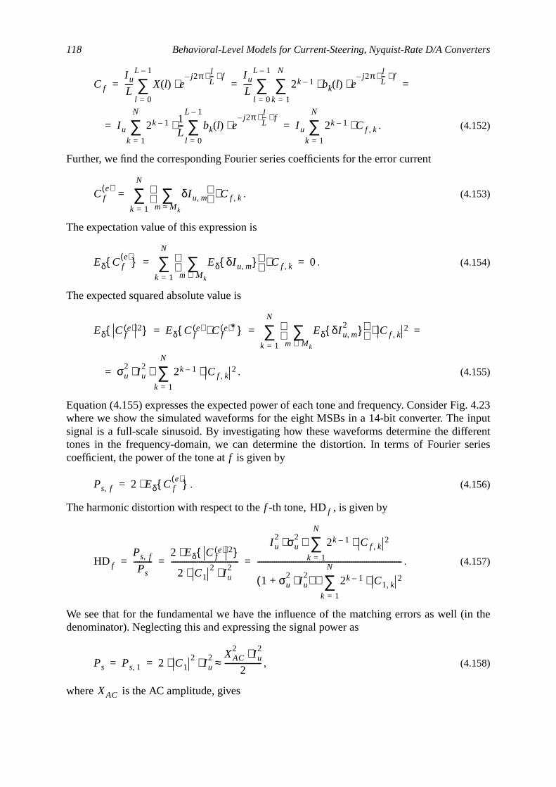
118 Behavioral-Level Models for Current-Steering, Nyquist-Rate D/A Converters
ig. 4.23inputerenteries
in the
. (4.152)
Further, we find the corresponding Fourier series coefficients for the error current
. (4.153)
The expectation value of this expression is
. (4.154)
The expected squared absolute value is
. (4.155)
Equation (4.155) expresses the expected power of each tone and frequency. Consider Fwhere we show the simulated waveforms for the eight MSBs in a 14-bit converter. Thesignal is a full-scale sinusoid. By investigating how these waveforms determine the difftones in the frequency-domain, we can determine the distortion. In terms of Fourier scoefficient, the power of the tone at is given by
. (4.156)
The harmonic distortion with respect to the -th tone, , is given by
. (4.157)
We see that for the fundamental we have the influence of the matching errors as well (denominator). Neglecting this and expressing the signal power as
, (4.158)
where is the AC amplitude, gives
Cf
I u
L---- X l( ) e
j2π lL--- f⋅ ⋅–
⋅l 0=
L 1–
∑I u
L---- 2k 1– bk l( )⋅
k 1=
N
∑ ej2π l
L--- f⋅ ⋅–
⋅l 0=
L 1–
∑= = =
I u 2k 1– 1L--- bk l( ) e
j2π lL--- f⋅ ⋅–
⋅l 0=
L 1–
∑⋅k 1=
N
∑ I u 2k 1– Cf k,⋅k 1=
N
∑= =
Cfe( ) δI u m,
m Mk≈∑
Cf k,⋅k 1=
N
∑=
Eδ Cfe( ) Eδ δI u m,
m Mk∈∑
Cf k,⋅k 1=
N
∑ 0= =
Eδ Cfe( ) 2 Eδ Cf
e( ) Cfe( )∗⋅ Eδ δI u m,
2 m Mk∈∑
Cf k,2⋅
k 1=
N
∑= = =
σu2
I u2
2k 1– Cf k,2⋅
k 1=
N
∑⋅ ⋅=
f
Ps f, 2 Eδ Cfe( ) ⋅=
f HD f
HD f
Ps f,Ps
----------2 Eδ Cf
e( ) 2 ⋅
2 C12
I u2⋅ ⋅
------------------------------------
I u2 σu
22k 1– Cf k,
2⋅k 1=
N
∑⋅ ⋅
1 σu2
I u2⋅+( ) 2k 1– C1 k,
2⋅k 1=
N
∑⋅
-----------------------------------------------------------------------------= = =
Ps Ps 1, 2 C12
I u2⋅ ⋅
XAC2
I u2⋅
2--------------------≈= =
XAC
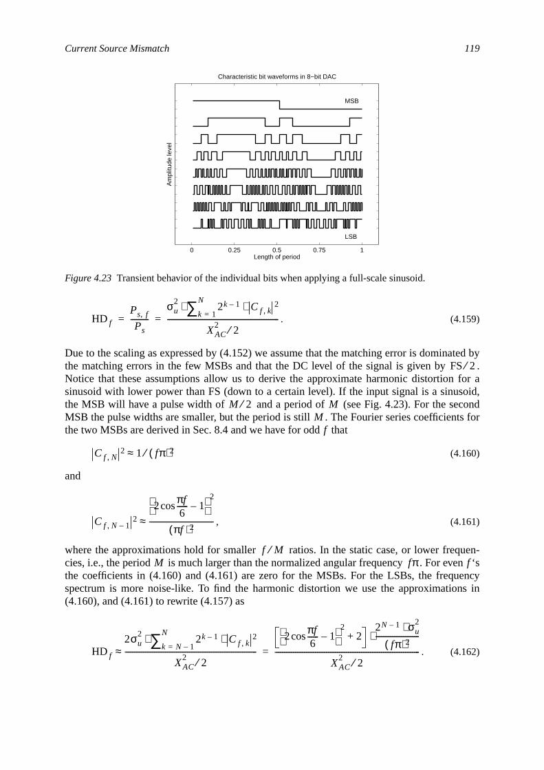
Current Source Mismatch 119
ted by.
for aoid,onds for
uen-n ‘sencyns in
. (4.159)
Due to the scaling as expressed by (4.152) we assume that the matching error is dominathe matching errors in the few MSBs and that the DC level of the signal is given byNotice that these assumptions allow us to derive the approximate harmonic distortionsinusoid with lower power than FS (down to a certain level). If the input signal is a sinusthe MSB will have a pulse width of and a period of (see Fig. 4.23). For the secMSB the pulse widths are smaller, but the period is still . The Fourier series coefficientthe two MSBs are derived in Sec. 8.4 and we have for odd that
(4.160)
and
, (4.161)
where the approximations hold for smaller ratios. In the static case, or lower freqcies, i.e., the period is much larger than the normalized angular frequency . For evethe coefficients in (4.160) and (4.161) are zero for the MSBs. For the LSBs, the frequspectrum is more noise-like. To find the harmonic distortion we use the approximatio(4.160), and (4.161) to rewrite (4.157) as
. (4.162)
Figure 4.23 Transient behavior of the individual bits when applying a full-scale sinusoid.
0 0.25 0.5 0.75 1
MSB
LSB
Characteristic bit waveforms in 8−bit DAC
Am
plitu
de le
vel
Length of period
HD f
Ps f,Ps
----------σu
22k 1– Cf k,
2⋅k 1=
N∑⋅
XAC2
2⁄-------------------------------------------------------------= =
FS 2⁄
M 2⁄ MM
f
Cf N,2 1 fπ( )2⁄≈
Cf N 1–,2
2 πf6------cos 1–
2
πf( )2-----------------------------------≈
f M⁄M fπ f
HD f
2σu2
2k 1– Cf k,2⋅
k N 1–=
N∑⋅
XAC2
2⁄------------------------------------------------------------------------≈
2 πf6------cos 1–
22+
2N 1– σu2⋅
fπ( )2------------------------⋅
XAC2
2⁄-------------------------------------------------------------------------------=
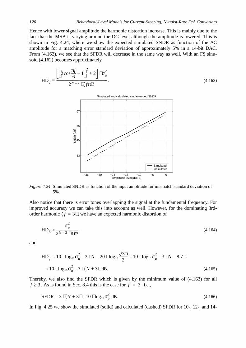
120 Behavioral-Level Models for Current-Steering, Nyquist-Rate D/A Converters
o theis is
ACAC.sinu-
y. For3rd-
all
d 14-
of
Hence with lower signal amplitude the harmonic distortion increase. This is mainly due tfact that the MSB is varying around the DC level although the amplitude is lowered. Thshown in Fig. 4.24, where we show the expected simulated SNDR as function of theamplitude for a matching error standard deviation of approximately 5% in a 14-bit DFrom (4.162), we see that the SFDR will decrease in the same way as well. With an FSsoid (4.162) becomes approximately
. (4.163)
Also notice that there is error tones overlapping the signal at the fundamental frequencimproved accuracy we can take this into account as well. However, for the dominatingorder harmonic , we have an expected harmonic distortion of
. (4.164)
and
dB. (4.165)
Thereby, we also find the SFDR which is given by the minimum value of (4.163) for. As is found in Sec. 8.4 this is the case for , i.e.,
dB. (4.166)
In Fig. 4.25 we show the simulated (solid) and calculated (dashed) SFDR for 10-, 12-, an
Figure 4.24 Simulated SNDR as function of the input amplitude for mismatch standard deviation5%.
HD f
2 πf6------cos 1–
22+ σu
2⋅
2N 2– fπ( )2⋅-------------------------------------------------------------≈
−36 −30 −24 −18 −12 −6 0
33
45
56
67
Simulated and calculated single−ended SNDR
SN
DR
[dB
]
Amplitude level [dBFS]
Simulated Calculated
f 3=( )
HD3
σu2
2N 2– 3π2⋅---------------------------≈
HD f 10 σu2
log10⋅ 3 N⋅– 203π2
----------log10⋅– 10 σu2
log10⋅ 3 N⋅– 8.7–≈ ≈ ≈
10 σu2
log10⋅ 3 N 3+( )⋅–≈
f 3≥ f 3=
SFDR 3 N 3+( )⋅ 10 σu2
log10⋅–≈
Current Source Mismatch 121
tion4.162)rs, thehtly
mula-5 are
ter7.8 onmeteredt arededonly
se thecom-
vesti-ented
ussianan beinear, the
bit DACs as function of the relative matching error. As we see there is a small deviabetween the simulated and calculated values. This depends on the approximation in (where only a few MSBs were considered. Since we are assuming uncorrelated erroerror power from all bits should be added to the specific tone. This would result in a sliglower calculated SFDR. The curves saturate for lower mismatch errors, since in the sitions the harmonics are hidden in the noise. The simulated results shown in Fig. 4.2found by taking the average from 1024 -point spectra for each mismatch value.
Influence of segmentation and thermometer codeA notation is that the distribution of the distortion terms will slightly differ for thermomecoded and segmented converters. Compare for example the simulation result Figurepage 202 where we have applied matching errors in a 8-bit converter that is fully thermocoded. There we find that it is thesecond harmonicthat determines performance. For thbinary converter it is thethird harmonic. This is due to the fact that for thermometer-codeDACs there is not the same fluctuation around the DC level in terms of number of bits thaswitching. With only one LSB changing around DC, all bits are changing in the binary-coDAC and hence much worse matching error than for the thermometer-coded DAC whereone bit changes. Secondly, the analysis must be slightly modified, since we cannot uapproach as examplified by Fig. 4.23. We get back to this issue in Chapter 5 where wepare measured with simulated results and the mathematical modeling is left for future ingation, where the aim is to generalize the expressions above to fit for a MSB segmconverter, where is arbitrary in the interval .
4.5.3 SNDR and SFDR as Function of the Graded andCorrelated Mismatch Errors
As was indicated, the matching errors cannot only be considered to be independent Gadistributed variables. In reality, the matching errors in two adjacent current sources chighly correlated. This is due to edge matching but also since we most likely have lgraded distribution of the matching errors over the array of unit current sources. Typically
Figure 4.25 Calculated and simulated SFDR as function of the mismatch for 10-, 12-, and 14-bitDACs.
216
10−4
10−3
10−2
10−1
40
60
80
100
11114
12
10
Simulated single−ended SFDRS
FD
R [d
B]
Mismatch standard deviation
KK 1 K N< <
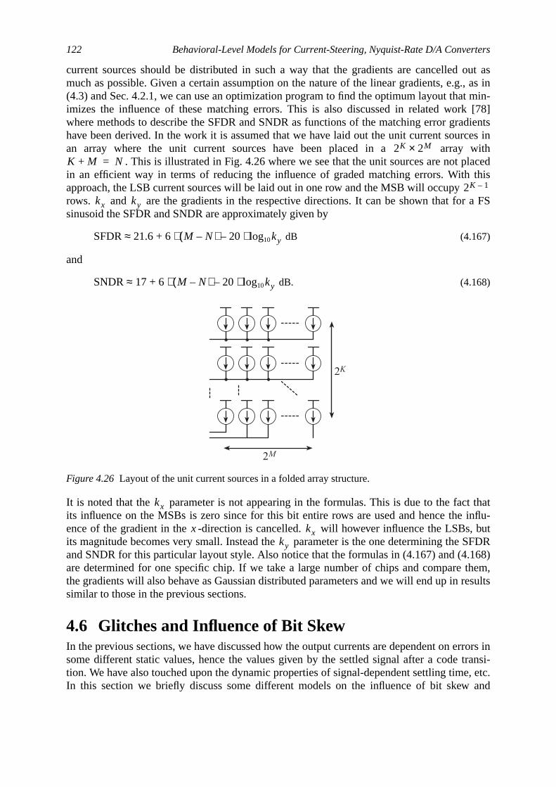
122 Behavioral-Level Models for Current-Steering, Nyquist-Rate D/A Converters
out as., as int min-
[78]dientsces inwith
acedthis
a FS
t thatinflu-
, butSFDR168)them,results
rrors intransi-e, etc.and
current sources should be distributed in such a way that the gradients are cancelledmuch as possible. Given a certain assumption on the nature of the linear gradients, e.g(4.3) and Sec. 4.2.1, we can use an optimization program to find the optimum layout thaimizes the influence of these matching errors. This is also discussed in related workwhere methods to describe the SFDR and SNDR as functions of the matching error grahave been derived. In the work it is assumed that we have laid out the unit current souran array where the unit current sources have been placed in a array
. This is illustrated in Fig. 4.26 where we see that the unit sources are not plin an efficient way in terms of reducing the influence of graded matching errors. Withapproach, the LSB current sources will be laid out in one row and the MSB will occupyrows. and are the gradients in the respective directions. It can be shown that forsinusoid the SFDR and SNDR are approximately given by
dB (4.167)
and
dB. (4.168)
It is noted that the parameter is not appearing in the formulas. This is due to the facits influence on the MSBs is zero since for this bit entire rows are used and hence theence of the gradient in the -direction is cancelled. will however influence the LSBsits magnitude becomes very small. Instead the parameter is the one determining theand SNDR for this particular layout style. Also notice that the formulas in (4.167) and (4.are determined for one specific chip. If we take a large number of chips and comparethe gradients will also behave as Gaussian distributed parameters and we will end up insimilar to those in the previous sections.
4.6 Glitches and Influence of Bit SkewIn the previous sections, we have discussed how the output currents are dependent on esome different static values, hence the values given by the settled signal after a codetion. We have also touched upon the dynamic properties of signal-dependent settling timIn this section we briefly discuss some different models on the influence of bit skew
Figure 4.26 Layout of the unit current sources in a folded array structure.
2K 2M×K M+ N=
2K 1–
kx ky
SFDR 21.6 6 M N–( )⋅ 20 kylog10⋅–+≈
SNDR 17 6 M N–( )⋅ 20 kylog10⋅–+≈
2K
2M
kx
x kxky
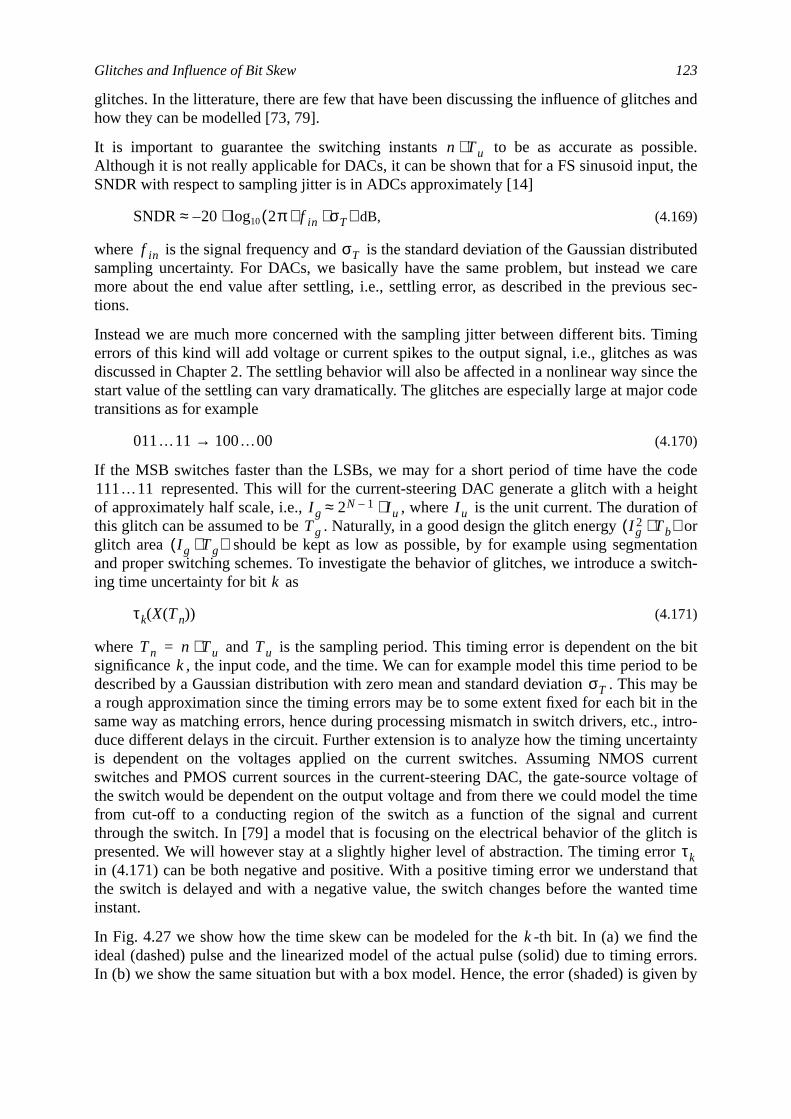
Glitches and Influence of Bit Skew 123
s and
sible.the
butedcare
s sec-
mingwase thecode
codeightofor
tationwitch-
bitto beay be
in the, intro-aintyrrent
age oftime
renth isrthat
d time
therrors.en by
glitches. In the litterature, there are few that have been discussing the influence of glitchehow they can be modelled [73, 79].
It is important to guarantee the switching instants to be as accurate as posAlthough it is not really applicable for DACs, it can be shown that for a FS sinusoid input,SNDR with respect to sampling jitter is in ADCs approximately [14]
dB, (4.169)
where is the signal frequency and is the standard deviation of the Gaussian distrisampling uncertainty. For DACs, we basically have the same problem, but instead wemore about the end value after settling, i.e., settling error, as described in the previoutions.
Instead we are much more concerned with the sampling jitter between different bits. Tierrors of this kind will add voltage or current spikes to the output signal, i.e., glitches asdiscussed in Chapter 2. The settling behavior will also be affected in a nonlinear way sincstart value of the settling can vary dramatically. The glitches are especially large at majortransitions as for example
(4.170)
If the MSB switches faster than the LSBs, we may for a short period of time have therepresented. This will for the current-steering DAC generate a glitch with a he
of approximately half scale, i.e., , where is the unit current. The durationthis glitch can be assumed to be . Naturally, in a good design the glitch energyglitch area should be kept as low as possible, by for example using segmenand proper switching schemes. To investigate the behavior of glitches, we introduce a sing time uncertainty for bit as
(4.171)
where and is the sampling period. This timing error is dependent on thesignificance , the input code, and the time. We can for example model this time perioddescribed by a Gaussian distribution with zero mean and standard deviation . This ma rough approximation since the timing errors may be to some extent fixed for each bitsame way as matching errors, hence during processing mismatch in switch drivers, etc.duce different delays in the circuit. Further extension is to analyze how the timing uncertis dependent on the voltages applied on the current switches. Assuming NMOS cuswitches and PMOS current sources in the current-steering DAC, the gate-source voltthe switch would be dependent on the output voltage and from there we could model thefrom cut-off to a conducting region of the switch as a function of the signal and curthrough the switch. In [79] a model that is focusing on the electrical behavior of the glitcpresented. We will however stay at a slightly higher level of abstraction. The timing erroin (4.171) can be both negative and positive. With a positive timing error we understandthe switch is delayed and with a negative value, the switch changes before the wanteinstant.
In Fig. 4.27 we show how the time skew can be modeled for the -th bit. In (a) we findideal (dashed) pulse and the linearized model of the actual pulse (solid) due to timing eIn (b) we show the same situation but with a box model. Hence, the error (shaded) is giv
n Tu⋅
SNDR 20– 2π f in σT⋅ ⋅( )log10⋅≈
f in σT
011…11 100…00→
111…11I g 2N 1– I u⋅≈ I uTg I g
2 Tb⋅( )I g Tg⋅( )
k
τk X Tn( )( )
Tn n Tu⋅= Tuk
σT
τk
k
124 Behavioral-Level Models for Current-Steering, Nyquist-Rate D/A Converters
off,notavever theega-from
fferentresult-boveo thecou-
put.roxi-for ande the
e
a square wave and not a triangular wave.
The switching activity in bit is denoted as
. (4.172)
If the switching activity is negative, we have that the bit goes from 1 to 0, hence is turnedit is positive if the bit goes from 0 to 1. If the switching activity is zero, the bit doeschange. A positive (4.171) together with a positive switching activity implies that we ha delayed signal and that we should subtract a pulse from the wanted result. A positiwith a negative switching activity implies that we should add a pulse. The same holds focase with a negative and positive switching activity. Finally, with a negative and ntive switching activity we should subtract a pulse. Therefore, we define the error pulse (Fig. 4.27 (b)) for positive as
. (4.173)
We can now describe the glitches in the time domain by
. (4.174)
We see that the glitches are described by several overlapping square-waves with didurations and amplitudes centered around the ideal sampling instants, . The overalling waveform will then most likely not be given by a square wave. The expression adepends on the unit current , the switching activity, and the time uncertainties and texpression, we have not added glitches arising from for example CFT or similar crosspling.
In Fig. 4.28 we show the simulated output spectra for a 14-bit DAC with FS sinusoid inThe timing errors are large to illustrate the effect, they have a standard deviation of appmately 5 per cent of the whole update period. Compare with (2.96) and (2.98) where we14-bit converter would require the glitch width to be in the order of % a
%, respectively. (The expressions assume maximum glitches and therefor
(a) (b)
Figure 4.27 Model of timing uncertainty. The ideal switching signal (dashed) is compared with thactual signal (solid). In (a) a linearized model and in (b) a box model.
t
bit k
t
bit k
k
∆bk Tn( ) bk Tn( ) bk Tn 1–( )–=
τkτk
τk τk
τk
Ukn( )
t( )
1– τk 0> Tn t Tn τk X Tn( )( )+≤ ≤
1 τk 0< Tn τk X Tn( )( )+ t Tn≤ ≤
0 else
=
G t( ) I u 2k 1– ∆bk Tn( ) Ukn( )
t( )⋅ ⋅k 1=
N
∑n 0=
∞
∑⋅=
N( )Tn
I u
7.4 10 7–⋅6.1 10 3–⋅
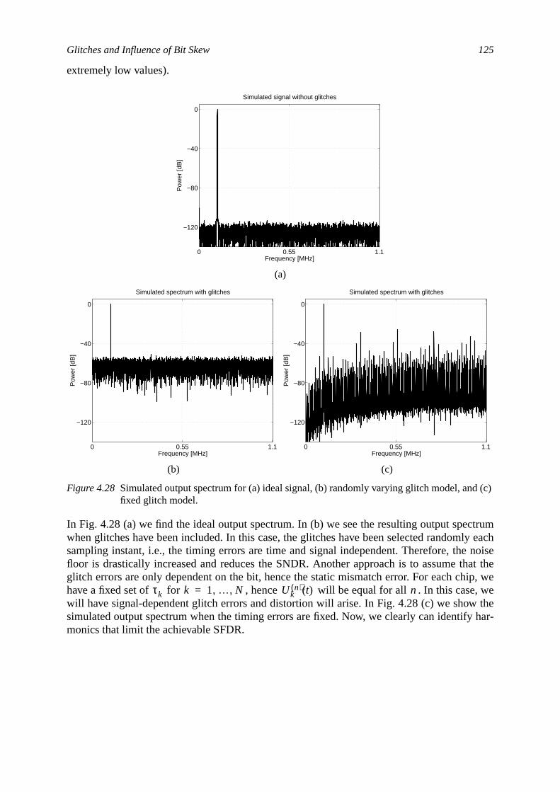
Glitches and Influence of Bit Skew 125
ctrumly eachnoiseat theip, wewethehar-
(c)
extremely low values).
In Fig. 4.28 (a) we find the ideal output spectrum. In (b) we see the resulting output spewhen glitches have been included. In this case, the glitches have been selected randomsampling instant, i.e., the timing errors are time and signal independent. Therefore, thefloor is drastically increased and reduces the SNDR. Another approach is to assume thglitch errors are only dependent on the bit, hence the static mismatch error. For each chhave a fixed set of for , hence will be equal for all . In this case,will have signal-dependent glitch errors and distortion will arise. In Fig. 4.28 (c) we showsimulated output spectrum when the timing errors are fixed. Now, we clearly can identifymonics that limit the achievable SFDR.
(a)
(b) (c)
Figure 4.28 Simulated output spectrum for (a) ideal signal, (b) randomly varying glitch model, andfixed glitch model.
0 0.55 1.1
−120
−80
−40
0
Simulated signal without glitches
Frequency [MHz]
Pow
er [d
B]
0 0.55 1.1
−120
−80
−40
0
Simulated spectrum with glitches
Frequency [MHz]
Pow
er [d
B]
0 0.55 1.1
−120
−80
−40
0
Simulated spectrum with glitches
Frequency [MHz]
Pow
er [d
B]
τk k 1 … N, ,= Ukn( ) t( ) n

126 Behavioral-Level Models for Current-Steering, Nyquist-Rate D/A Converters
Wee.
idatess notomeented
lad-R–2Rtead,
ourcesthes with
es for
at per-ce the
rrenta. Theon theSNR,ore, asually as the
ected,
5 Current-Steering D/AConverters
5.1 IntroductionIn this chapter we present work on circuit implementations of different D/A converters.discuss how the proposed formulas from the previous chapter relates to the design phas
Throughout the thesis, we have identified the current-steering DAC as a suitable candfor high-speed and high-resolution communication applications. This architecture doeneed any output buffer as for example the switched-capacitor DAC. It will however becsensitive to finite output impedance. Further, the current-steering DAC can be implemwith MOS-only components and still reach rather high accuracy. Resistor-string or R–2Rders are also very fast, but they require high-accuracy on-chip resistors. Although thearchitecture is a current-steering DAC, it will not be further addressed in this chapter. Inswe focus on the pure current-steering versions where a number of weighted current sare used to form the conversion function. An overview of different layout strategies forunit current sources is given in Sec. 5.2. We highlight the advantages and disadvantagethe different topologies. For some of the topologies there are inhereted good propertihigh performance.
In Sec. 5.3 we discuss some practical design issues. In the previous chapter we found thformance is strongly dependent on e.g. the output impedance of the current sources sinlinearity is degraded. The circuit noise is determined by the DC output current of a cusource and matching is practically determined by the transistor size, i.e., the gate areoutput impedance is dependent on the DC current and the DC current is dependenttransistor size, etc. When increasing the output current with the ambition to improve thethe output impedance is decreasing and thereby the nonlinearity increase, etc. Therefalways in analog design, we have a delicate relation between design parameters and ustrade-off has to be done. Further the influence of clock feedthrough in switches as well aon-resistance is crucial. Also the influence of the interconnecting wires must not be negl
127
128 Current-Steering D/A Converters
enta--offsresultsi-tonevaria-
t with
onceitches.by thered)low-aboutrfor-
, goodurrentthense spe-t the
pute ratio
nduc-to
etc.
To further illustrate the current-steering architecture, we present the results from implemtion of wideband CMOS DACs for xDSL applications in Sec. 5.4. We show design tradeand ideas on how to implement the required circuit elements. Measured and simulatedfrom the wideband DAC are discussed in Sec. 5.5. Output spectra from single- and multmeasurements are shown. We also compare the results from two similar DACs that havetions in design of the unit current sources and interconnection wires. We have found thaa small variation in layout, an SFDR improvement of over 12 dB is achieved.
5.2 Current-Steering DAC ArchitecturesThe current-steering DAC architecture was described in Sec. 3.6.1 and the structure isagain sketched in Fig. 5.1 for convenience. There is a number of current sources and swDepending on the input code, , the current from the corresponding sources is directedswitches to the output and terminated by an off-chip resistor or I/V converted (and filteusing a buffer at the output as shaded in the figure. The output buffer will guarantee aimpedance node at the output of the DAC and hence we do not have to worry as muchthe limited output impedance. Instead the matching errors will strongly influence the pemance. This was also discussed in the previous chapter and as is commonly knownmatching of the current sources is reuiqred for high performance. Instead of using a csource with the nominal value one uses unit current sources in parallel. We willhave the same type of edge matching errors for each element. Secondly, we may also ucial layout techniques, such as interdigitized or common-centroid in order to smooth ouinfluence of graded mismatch errors.
If no buffer amplifier is used at the output, the DAC will be sensitive to the limited outimpedance. As found in Sec. 4.3 the SNDR and SFDR are dependent on the conductanc
, (5.1)
where is the output conductance of the unit current source and is the load cotance. Typically, with an output buffer, this will become approximately zero, , due
Figure 5.1 Principle of anN-bit current-steering DAC.
X
M M
ILSB2N-1ILSB 2N-2ILSB
bN bN-1 b1
Iout(t)
RL
ρG GS GL⁄=
GS GLGL 0≈
Current-Steering DAC Architectures 129
r large.the dis-
transis-zero.rrentnd ,ign ofg, the
of theout
ourcescur-rcesvioussensi-
andThisdirec-
the virtual ground at the input of the amplifier.
To guarantee good matching we need the gate areas of the current sources to be ratheWe have that the matching is inversely dependent on the gate area of the transistor andtance between the transistors that should be matched [68], e.g.,
, (5.2)
where and is a process-dependent parameter and is the distance to anothertor. Hence we want the area to go towards infinity and the distance to go towardsObviously, this is a contradiction, since one of the main targets is to lay out the cusources as close to each other as well. The design issue is to find the optimum awhere the parameter is a function of the and . This is discussed more in the desunit current sources in Sec. 5.3.1. Since we will occupy a large area for good matchintotal area of the DAC will become very large.
To the matching errors and output impedance issues, we also have to add the influenceinterconnection wires. In the following we discuss some different approaches for layingthe unit current sources.
5.2.1 Flat and Folded Array StructuresThe first, simplest, and perhaps the most naive approach is to lay out the unit current sas shown in Fig. 5.2 (a). The MSB current source is formed by taking parallel unitrent sources in one row. The second MSB is formed in the similar way with soufrom another row, etc. Each row is interconnected and fed to a current switch. It is obthat the array becomes very wide for a higher number of bits. The DAC also becomestive to matching gradients.
The natural and obvious way to circumvent this is for the MSBs to use more than one rowfor the LSBs to use the same row as illustrated by the “folded” approach in Fig. 5.2 (b).also makes the converter less sensitive to linear graded mismatch errors in at least one
(a) (b)
Figure 5.2 (a) “Flat” and (b) “folded” array layout of unit current sources.
σ2 ∆I( )AβWL-------- Ad D2⋅+=
Aβ Ad DWL D
W LD W L
2N 1–
2N 2–
IN
IN-1
I2
I1
IN
IK
I2
I1
IK-1
130 Current-Steering D/A Converters
icateveral
ents on
ributeDACsoci-gradi-ces is
from
isbeen
havemorenoiset thean begths,
tion [78]. To relax the design of interconnection wires, one could for the MSBs also duplthe digital logic circuits and for example use one switch for each row and hence seswitches for the same bit operating in parallel.
These approaches, however, are not suitable for higher resolutions, due to the requiremparasitic resistance in switches and wires as well as the current source matching.
To make the DAC even less sensitive to matching gradients one should preferrably distthe current sources over the array as illustrated in Fig. 5.3 for a 6-bit binary-weightedwith 63 unit current sources. The numbers indicate to which bit the current source is asated. We assume that the matching errors are approximately given by a plane and theents are rather large, and that the distance between the unit current sourunity in both directions.
Further we assume that the zero value is at the center of the array. Using the equation(4.3) we find that the upper left current source would have the nominal value
(5.3)
and the lower right
, (5.4)
etc. In Fig. 5.3 (b) we discuss how this affects the INL of the DAC, the maximum INLapproximately 3 LSB. In Fig. 5.4 we show an approach when the current sources havelaid out in a more random manner. We find that the impact on INL is much lower (b). Wethat the maximum INL is about 0.2 LSB. However, the approach in Fig. 5.4 (a) requirescomplex routing of the interconnecting wires, etc. This will increase the parasitics andlevels. Notice that the distribution of the current sources examplified in Fig. 5.4 (a) is nooptimal one, it has been done by hand. With a computer program, the optimal layout cfound. Further, we can add cost functions such as the impact on DNL and INL, wire lenselection algorithms, etc.
(a) (b)
Figure 5.3 Influence of gradients for a (a) flat layout approach on the (b) INL.
ky kx 0.05= =
6 6 6 6 6 6 6 6
6 6 6 6 6 6 6 6
6 6 6 6 6 6 6 6
6 6 6 6 6 6 6 6
5 5 5 5 5 5 5 5
5 5 5 5 5 5 5 5
4 4 4 4 4 4 4 4
0 1 2 2 3 3 3 3
DAC unit current source array
10 20 30 40 50 60−4
−3
−2
−1
0
1
2
3
4INL for best−fit line
INL
[LS
B]
Input code
I u 1, I u 3.5 kx⋅– 3.5 ky⋅+=
I u 63, I u 3.5 kx⋅ 3.5 ky⋅–+=
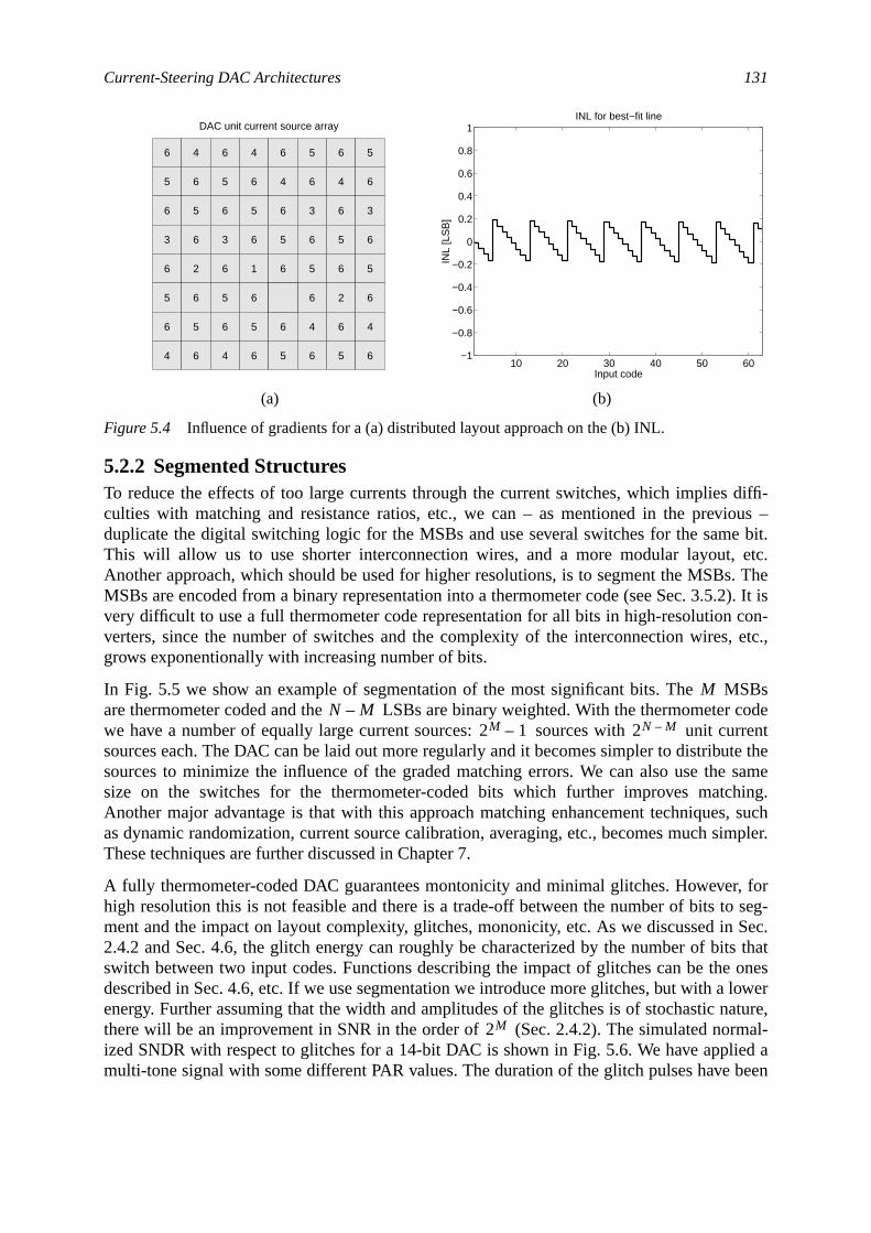
Current-Steering DAC Architectures 131
diffi-ous –e bit.etc.. The
2). It iscon-, etc.,
SBscode
rrentte thesame
hing., such
impler.
, forseg-Sec.
ts thatones
lowerature,mal-ed abeen
5.2.2 Segmented StructuresTo reduce the effects of too large currents through the current switches, which impliesculties with matching and resistance ratios, etc., we can – as mentioned in the previduplicate the digital switching logic for the MSBs and use several switches for the samThis will allow us to use shorter interconnection wires, and a more modular layout,Another approach, which should be used for higher resolutions, is to segment the MSBsMSBs are encoded from a binary representation into a thermometer code (see Sec. 3.5.very difficult to use a full thermometer code representation for all bits in high-resolutionverters, since the number of switches and the complexity of the interconnection wiresgrows exponentionally with increasing number of bits.
In Fig. 5.5 we show an example of segmentation of the most significant bits. The Mare thermometer coded and the LSBs are binary weighted. With the thermometerwe have a number of equally large current sources: sources with unit cusources each. The DAC can be laid out more regularly and it becomes simpler to distribusources to minimize the influence of the graded matching errors. We can also use thesize on the switches for the thermometer-coded bits which further improves matcAnother major advantage is that with this approach matching enhancement techniquesas dynamic randomization, current source calibration, averaging, etc., becomes much sThese techniques are further discussed in Chapter 7.
A fully thermometer-coded DAC guarantees montonicity and minimal glitches. Howeverhigh resolution this is not feasible and there is a trade-off between the number of bits toment and the impact on layout complexity, glitches, mononicity, etc. As we discussed in2.4.2 and Sec. 4.6, the glitch energy can roughly be characterized by the number of biswitch between two input codes. Functions describing the impact of glitches can be thedescribed in Sec. 4.6, etc. If we use segmentation we introduce more glitches, but with aenergy. Further assuming that the width and amplitudes of the glitches is of stochastic nthere will be an improvement in SNR in the order of (Sec. 2.4.2). The simulated norized SNDR with respect to glitches for a 14-bit DAC is shown in Fig. 5.6. We have applimulti-tone signal with some different PAR values. The duration of the glitch pulses have
(a) (b)
Figure 5.4 Influence of gradients for a (a) distributed layout approach on the (b) INL.
6 4 6 4 6 5 6 5
5 6 5 6 4 6 4 6
6 5 6 5 6 3 6 3
3 6 3 6 5 6 5 6
6 2 6 1 6 5 6 5
5 6 5 6 0 6 2 6
6 5 6 5 6 4 6 4
4 6 4 6 5 6 5 6
DAC unit current source array
10 20 30 40 50 60−1
−0.8
−0.6
−0.4
−0.2
0
0.2
0.4
0.6
0.8
1INL for best−fit line
INL
[LS
B]
Input code
MN M–
2M 1– 2N M–
2M
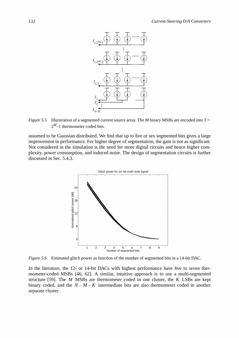
132 Current-Steering D/A Converters
a largeficant.com-rther
ther-ntedkeptother
assumed to be Gaussian distributed. We find that up to five or sex segmented bits givesimprovement in performance. For higher degree of segmentation, the gain is not as signiNot considered in the simulation is the need for more digital circuits and hence higherplexity, power consumption, and induced noise. The design of segmentation circuits is fudiscussed in Sec. 5.4.3.
In the literature, the 12- or 14-bit DACs with highest performance have five to sevenmometer-coded MSBs [46, 62]. A similar, intuitive approach is to use a multi-segmestructure [59]. The MSBs are thermometer coded in one cluster, the LSBs arebinary coded, and the intermediate bits are also thermometer coded in anseparate cluster.
Figure 5.5 Illurstration of a segmented current source array. TheM binary MSBs are encoded intoT =
2M–1 thermometer coded bits.
Figure 5.6 Estimated glitch power as function of the number of segmented bits in a 14-bit DAC.
Is,2M-1
I2
I1
IN-M
Is,2M-2
Is,1
1 2 3 4 5 6 7 8 9
0
6
12
18
24
Glitch power for 14−bit multi−tone signal
Nor
mal
ized
glit
ch p
ower
[dB
]
Number of segmented bits
M KN M– K–
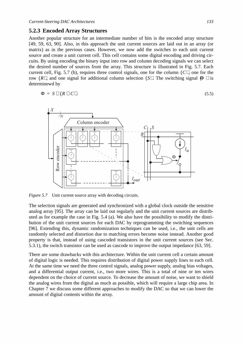
Current-Steering DAC Architectures 133
cturey (orurrentg cir-electEachr the
is
nsitiveistrib-istri-nces
ls arer goode Sec.3, 59].
ountcell.ltages,iresshielda. Iner the
5.2.3 Encoded Array StructuresAnother popular structure for an intermediate number of bits is the encoded array stru[49, 59, 63, 90]. Also, in this approach the unit current sources are laid out in an arramatrix) as in the previous cases. However, we now add the switches to each unit csource and create a unit current cell. This cell contains some digital encoding and drivincuits. By using encoding the binary input into row and column decoding signals we can sthe desired number of sources from the array. This structure is illustrated in Fig. 5.7.current cell, Fig. 5.7 (b), requires three control signals, one for the column , one forow , and one signal for additional column selection . The switching signaldeterminewd by
. (5.5)
The selection signals are generated and synchronized with a global clock outside the seanalog array [95]. The array can be laid out regularly and the unit current sources are duted as for example the case in Fig. 5.4 (a). We also have the possibility to modify the dbution of the unit current sources for each DAC by reprogramming the switching seque[96]. Extending this, dynamic randomization techniques can be used, i.e., the unit celrandomly selected and distortion due to matching errors become noise instead. Anotheproperty is that, instead of using cascoded transistors in the unit current sources (se5.3.1), the switch transistor can be used as cascode to improve the output impedance [6
There are some drawbacks with this architecture. Within the unit current cell a certain amof digital logic is needed. This requires distribution of digital power supply lines to eachAt the same time we need the three control signals, analog power supply, analog bias voand a differential output current, i.e., two more wires. This is a total of nine or ten wdependent on the choice of current source. To decrease the amount of noise, we want tothe analog wires from the digital as much as possible, which will require a large chip areChapter 7 we discuss some different approaches to modify the DAC so that we can lowamount of digital contents within the array.
Figure 5.7 Unit current source array with decoding circuits.
C( )R( ) S( ) Φ( )
Φ S R C∧( )∨=
Column encoder
Row
enc
oder
Iout
SR
C
F
XN
Iu
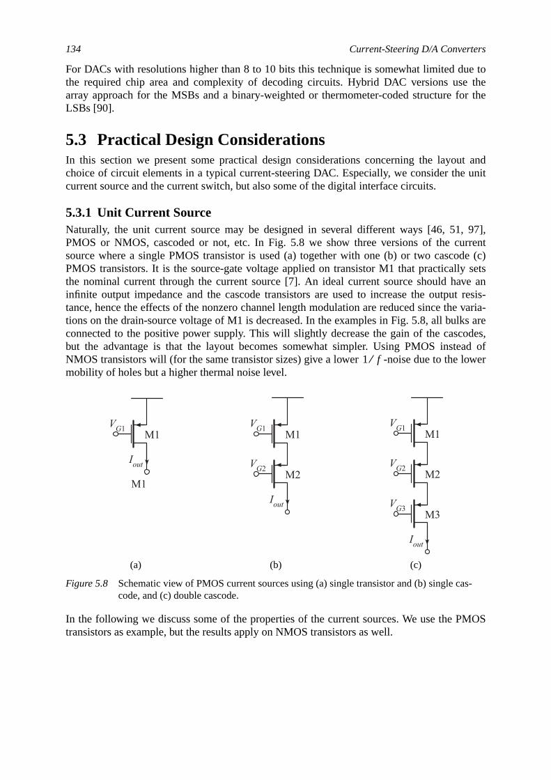
134 Current-Steering D/A Converters
e tothe
or the
t andunit
97],rrentde (c)
setsve ant resis-
varia-s are
odes,ad of
ower
MOS
as-
For DACs with resolutions higher than 8 to 10 bits this technique is somewhat limited duthe required chip area and complexity of decoding circuits. Hybrid DAC versions usearray approach for the MSBs and a binary-weighted or thermometer-coded structure fLSBs [90].
5.3 Practical Design ConsiderationsIn this section we present some practical design considerations concerning the layouchoice of circuit elements in a typical current-steering DAC. Especially, we consider thecurrent source and the current switch, but also some of the digital interface circuits.
5.3.1 Unit Current SourceNaturally, the unit current source may be designed in several different ways [46, 51,PMOS or NMOS, cascoded or not, etc. In Fig. 5.8 we show three versions of the cusource where a single PMOS transistor is used (a) together with one (b) or two cascoPMOS transistors. It is the source-gate voltage applied on transistor M1 that practicallythe nominal current through the current source [7]. An ideal current source should hainfinite output impedance and the cascode transistors are used to increase the outputance, hence the effects of the nonzero channel length modulation are reduced since thetions on the drain-source voltage of M1 is decreased. In the examples in Fig. 5.8, all bulkconnected to the positive power supply. This will slightly decrease the gain of the cascbut the advantage is that the layout becomes somewhat simpler. Using PMOS insteNMOS transistors will (for the same transistor sizes) give a lower -noise due to the lmobility of holes but a higher thermal noise level.
In the following we discuss some of the properties of the current sources. We use the Ptransistors as example, but the results apply on NMOS transistors as well.
(a) (b) (c)
Figure 5.8 Schematic view of PMOS current sources using (a) single transistor and (b) single ccode, and (c) double cascode.
1 f⁄
VG1
Iout
M1
M1VG1
VG2
Iout
M1
M2
VG1
VG2
VG3
Iout
M1
M2
M3
Practical Design Considerations 135
er we. The
,
ctor,sourcesed by
, ist
satura- [7]
paci-gate
annel
t
d withurcesd theere
are
, it isended
Output impedanceWe require a very high output resistance for high performance. In the previous chaptfound that the SFDR and SNDR are highly dependent on a nonzero conductance ratiooutput resistance for the sources in Fig. 5.8 (a) through (c) are denoted , , andrespectively, and they are approximately given by [7]
, , and . (5.6)
where is the DC output current of the source, is the channel length modulation fais the transconductance parameter, and is a parameter determined by the bulk-
transconductance of the transistors. The output resistance of the current source is increaa factor corresponding to the approximate gain of the cascode transistor. The current,mostly set by the specification, e.g., with a 1-V swing over a 50-Ω termination the peak outpucurrent is 20 mA. In a 14-bit DAC, we then get the LSB current as
. (5.7)
For high output resistance we must guarantee that the transistors are operating in theirtion regions. The output current of the unit current source is then approximately given by
, (5.8)
where is the transconductance parameter, is the charge mobility, is the catance per gate area, is the transistor’s size aspect ratio, and is the effectivevoltage. Further, the channel length modulation factor is inversely dependent on the chlength [7], . Since the current is fixed by the specification, we have that
. (5.9)
For high resistance we require long channels. For the cascoded current sources, we ge
and , (5.10)
hence for high output resistance we require large cascode transistors.
The current source will have an output pole due to the parasitic capacitances associatethe transistors. In Fig. 5.9 we show the simulated output impedance for three current soas the examples in Fig. 5.8. In the simulations a 0.6- CMOS process was used angate widths of all transistors were equal, , but the channel lengths w
, , and . The currents through the current sourcesapproximately 1.22µA.
From Fig. 5.9 we clearly see the output resistance is improved by using cascodesimproved from approximately 300 MΩ to 30 TΩ. Using the results from the models in thprevious chapter (4.90), we have that if the SNDR of the 14-bit converter in the single-ecase for an FS sinusoid should be higher than say 80 dB we get
Ra Rb Rc
Ra1
λ1 I u⋅---------------≈ Rb Ra
1 η2+( ) 2β2
λ2 I u⋅----------------------------------⋅≈ Rc Rb
1 η3+( ) 2β3
λ3 I u⋅----------------------------------⋅≈
I u λiβi ηi
I u
203–×10
214 1–-------------------- 1.22 µA≈
I u
β1
2----- Veff
2⋅≈µ0 p, Cox
2-------------------- W
L----- Veff
2⋅ ⋅=
β1 µ0 p, CoxW L⁄ Veff
λ 1 L⁄∼
Ra L1∼
Rb L1 W2L2⋅∼ Rc L1 W2L2 W3 L3⋅⋅ ⋅∼
µmW 2 µm=
L1 8 µm= L2 2 µm= L3 1.2 µm=
136 Current-Steering D/A Converters
-
- androach.due tosameat the
e thatat the
nd thein-bulk
is
. (5.11)
This gives an upper bound on the output conductance as
, (5.12)
where is the load conductance. With a 50-Ω load we get the maximum unit output conductance as
. (5.13)
This corresponds to an output resistance of
. (5.14)
We see from the simulation results in Fig. 5.9 that this requirement is met for the singledouble-cascoded current source configurations, but not for the single transistor appHowever, for higher frequencies the output impedance is decreasing by 20 dB/decadethe output poles. At higher frequencies (above 50 kHz), all sources basically have theimpedance characteristics. Although it is a somewhat rough approach, we can see thbound in (5.14) cannot be guaranteed for frequencies above only 630Ω for the cascoded cur-rent sources.
These limitations are due to the capacitive parts of the current source and if we assumthe cascodes’ gains are rather high the dominating capacitances will be the ones founddrains closest to the outputs. These are typically the gate-drain overlap capacitance adrain-bulk capacitance. The overlap capacitance can be neglected and we have the dracapacitance given by [7]
, (5.15)
where is the drain area and is the junction capacitance per drain area.
Figure 5.9 Simulated output impedance of three different unit current source configurations.
0.2 45 16k 1M 1G
292M
6.3G
104G
29T
Frequency [Hz]
Impe
danc
e [Ω
]
Output impedance of current sources
Double cascode Single cascode Single transistor
SNDR 6 14 0.4–( )– 20 ρGlog10⋅– 80>≈ ρG 7.949–×10<⇒
GS 2.4428–×10 GL⋅<
GL
GS 1.58910–×10<
RS 6.29GΩ>
Cdb Ad Cjd⋅≈
Ad W Ld⋅= Cjd Ld
Practical Design Considerations 137
n the
ined
rs theto bethsce can
sup-0 wece for
fromthe
h the-ance ise, thesourcetran-
atchingvaria-errorstochas-in thevari-e dis-rocesse a
riving
the drain length. Approximately, we get that the capacitance is linearly dependent owidth
. (5.16)
The output poles for the current sources in Fig. 5.8 (a) through (b) can roughly be determby combining (5.6), (5.9), (5.10), and (5.16). We get some approximate relations as
, , and
. (5.17)
From this we have the intuitive result that the larger we make the widths of the transistolower pole. In an implementation, it can be advantegous to choose all transistor widthsequal since the layout becomes somewhat simpler. In that case, we end up with the lengas design parameters. More analysis on the influence of the pole in the unit current sourbe found in e.g. [126].
Another interesting design issue is how the current sources react on variations of the DCply voltage and the DC voltage applied at the output of the current source. In Fig. 5.1show the simulated output impedance for the single-cascoded (Fig. 5.8 (b)) current sourdifferent supply and output voltage levels. In Fig. 5.10 (a) we vary the supply voltage2.2 V to 5 V and the output voltage level is held constant at 0.5 V. In Fig. 5.10 (b) we fixsupply voltage at 5 V and the output voltage is varied from 0 to 1.2 V. The current througsource is kept nearly constant and equal to 1.22µA. We find that the output resistance is linearly depdent on supply and output voltage variations and hence as expected the impeddependent on the current through the mirror and due to the high output impedancchanges are relatively small. From Fig. 5.10 (a) we see for the double cascode currentthat a minimum supply voltage of approximately 3.2 V is required, since otherwise thesistors work in the linear regions.
MatchingAs we have discussed in the previous sections, there are several sources for the merrors, i.e., transistor size errors, threshold voltag variations, supply and bias voltagestions, oxide thickness variations, output voltage variations, etc. The graded matchingcan be minimized by spreading out the unit current sources as smart as possible. The stic matching must be minimized through proper choice of transistor sizes. From studiesliterature [41, 49] we know that the - and -matching are uncorrelated and that theirance is inversely proportional to the transistor area, and linearly dependent on thtance between the objects to match. If the different parameters are provided by the pdistributor, we can find a trade-off yielding the minimum error. For example, if we havrather simplified formula as
, (5.18)
where are the process-dependent parameters. The minimum is found by de(5.18) with respect to the widht and length:
Cdb W∼
ωa1
Ra Cgd a,⋅------------------------ 1
L1 W1⋅------------------∼≈ ωb
1Rb Cgd b,⋅------------------------ 1
L1----- 1
L2
---------- 1
W23 2⁄-------------⋅ ⋅∼≈
ωc1
Rc Cgd c,⋅----------------------- 1
L1----- 1
L2
---------- 1
L3
---------- 1
W2
------------ 1
W33 2⁄-------------⋅ ⋅ ⋅ ⋅∼≈
Li
β VTWL
σ2 ab
WL-------- c W2⋅ d L2⋅ e WL⋅+ + + +=
a b c d e, , , ,
138 Current-Steering D/A Converters
, withthe
f opti-
ue tod the
e tran-r andtioncurate1 wed aslarge.
g theentrrent, i.e.,
volt-
(5.19)
and
. (5.20)
From (5.19) and (5.20) we get for example
. (5.21)
Typically, we have that the larger transistors we choose, the better matching. Howeverlarger widths the output pole will move towards the origin. A natural choice is to choosegate length of the source transistor to be large. Further examples on the calculation omum sizes can be found in for example [98, 99].
Matching errors similar to those of graded oxide variations and similar may also arise dpoorly designed interconnection wires [69, 100]. We have that the output resistance anoutput current is dependent on the bias voltage applied on the gate voltage of the sourcsistors M1. The voltage is generated by a bias current, which basically is a current mirrothe reference current through the primary side of the mirror is controlled by a terminaresistance. However, especially for high resolutions, we have to guarantee that very acand equal bias and supply voltages are supplied to all unit current sources. In Fig. 5.1illustrate the effects of voltage loss over for example the supply wire. The wire is modelea number of resistances in series. In a regular layout these resistances are all equallySince we are tapping current through the unit sources, we will have voltage drops alonsupply wire. With the directions used in the figure, we have . Dependon layout style, the currents, , are typically determined by a number of parallel unit cusources. Further on, the current , is given by the effective voltage according to (5.8)
(a) (b)
Figure 5.10 Simulated output impedance of the unit current sources as function of the (a) supplyage and (b) output DC voltage level.
2 2.5 3 3.5 4 4.5 5
10M
1G
1T
100T
Supply voltage [V]
Out
put r
esis
tanc
e [Ω
]Output resistance vs. supply voltage
Double cascode Single cascode Single transistor
0 0.2 0.4 0.6 0.8 1 1.2
10M
1G
1T
100T
Output DC voltage [V]
Out
put r
esis
tanc
e [Ω
]
Output resistance vs. output voltage
Double cascode Single cascode Single transistor
σ2∂W∂
--------- 2c W⋅ e L⋅ bW2L-----------–+ 0 2c W3L⋅ e W2L2⋅ b–+⇒ 0= = =
σ2∂L∂
--------- 2d L⋅ e W⋅ bW L2-----------–+ 0 2d L3W⋅ e W2L2⋅ b–+⇒ 0= = =
2c W3L⋅ 2d L3W⋅=WL-----⇒ d
c---=
VDD V1 … VN> > >I i
I i
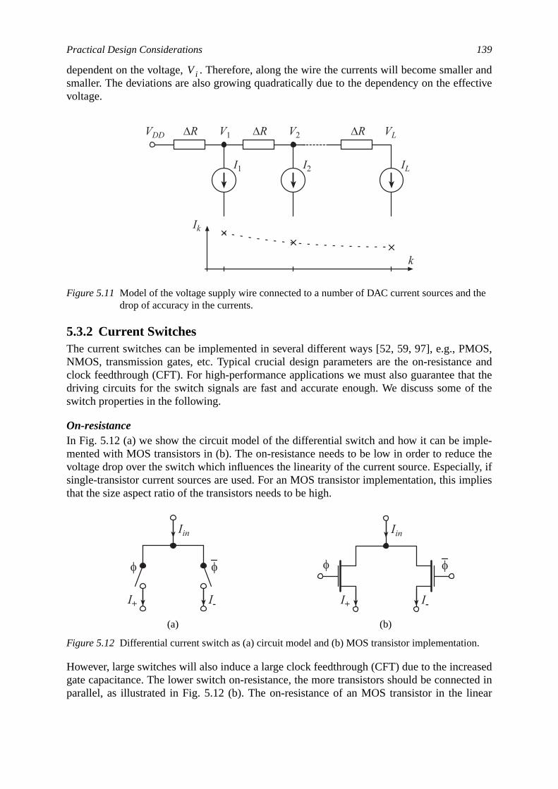
Practical Design Considerations 139
r andective
MOS,ce andat theof the
ple-ce thelly, ifplies
asedcted in
inear
the
.
dependent on the voltage, . Therefore, along the wire the currents will become smallesmaller. The deviations are also growing quadratically due to the dependency on the effvoltage.
5.3.2 Current SwitchesThe current switches can be implemented in several different ways [52, 59, 97], e.g., PNMOS, transmission gates, etc. Typical crucial design parameters are the on-resistanclock feedthrough (CFT). For high-performance applications we must also guarantee thdriving circuits for the switch signals are fast and accurate enough. We discuss someswitch properties in the following.
On-resistanceIn Fig. 5.12 (a) we show the circuit model of the differential switch and how it can be immented with MOS transistors in (b). The on-resistance needs to be low in order to reduvoltage drop over the switch which influences the linearity of the current source. Especiasingle-transistor current sources are used. For an MOS transistor implementation, this imthat the size aspect ratio of the transistors needs to be high.
However, large switches will also induce a large clock feedthrough (CFT) due to the incregate capacitance. The lower switch on-resistance, the more transistors should be conneparallel, as illustrated in Fig. 5.12 (b). The on-resistance of an MOS transistor in the l
Figure 5.11 Model of the voltage supply wire connected to a number of DAC current sources anddrop of accuracy in the currents.
(a) (b)
Figure 5.12 Differential current switch as (a) circuit model and (b) MOS transistor implementation
Vi
VDD DR DR DRV1 V2 VL
I1 I2 IL
Ik
k
I+
Iin
I-
f f
I+
Iin
I-
f f
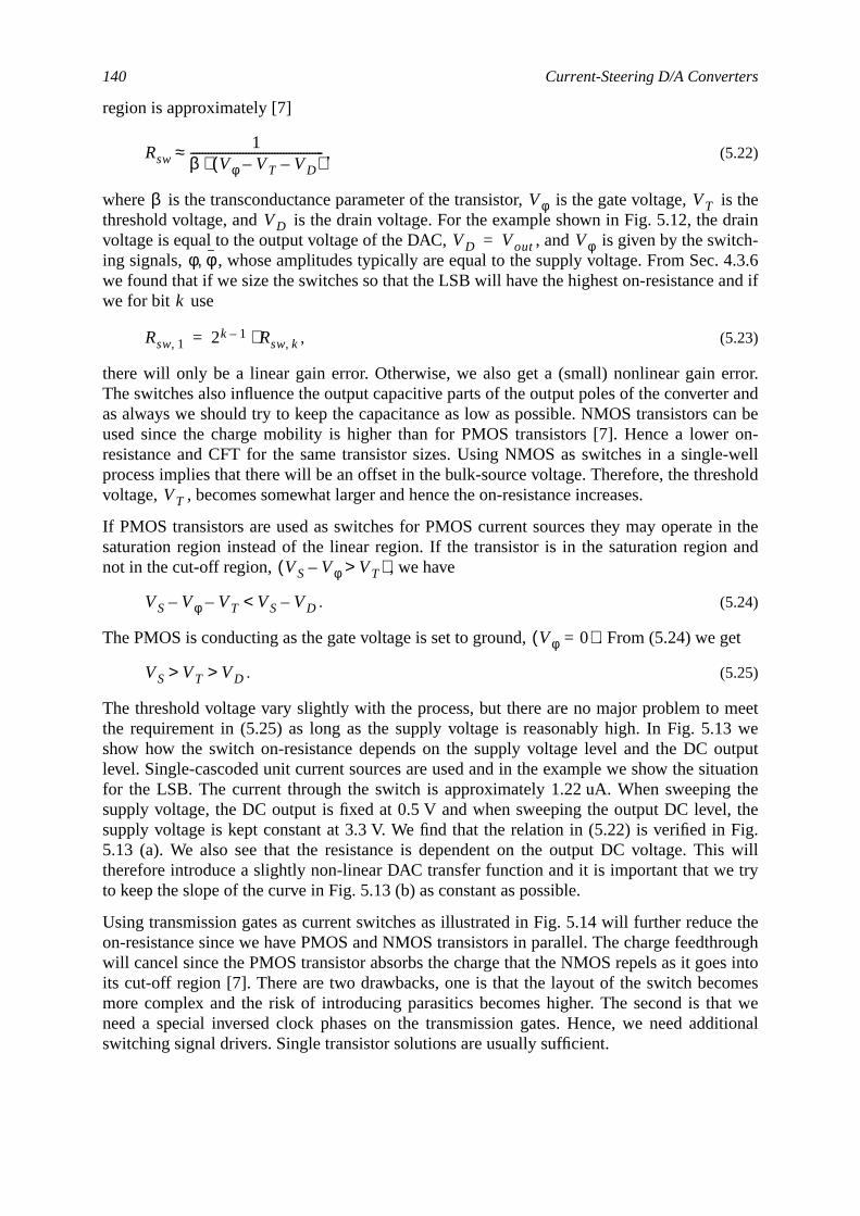
140 Current-Steering D/A Converters
is thedraintch-4.3.6and if
rror.er andcan ber on-e-wellshold
in theand
get
meet3 we
outputituation
thel, theFig.is willtry
e theroughs intomesat weditional
region is approximately [7]
, (5.22)
where is the transconductance parameter of the transistor, is the gate voltage,threshold voltage, and is the drain voltage. For the example shown in Fig. 5.12, thevoltage is equal to the output voltage of the DAC, , and is given by the swiing signals, , whose amplitudes typically are equal to the supply voltage. From Sec.we found that if we size the switches so that the LSB will have the highest on-resistancewe for bit use
, (5.23)
there will only be a linear gain error. Otherwise, we also get a (small) nonlinear gain eThe switches also influence the output capacitive parts of the output poles of the convertas always we should try to keep the capacitance as low as possible. NMOS transistorsused since the charge mobility is higher than for PMOS transistors [7]. Hence a loweresistance and CFT for the same transistor sizes. Using NMOS as switches in a singlprocess implies that there will be an offset in the bulk-source voltage. Therefore, the threvoltage, , becomes somewhat larger and hence the on-resistance increases.
If PMOS transistors are used as switches for PMOS current sources they may operatesaturation region instead of the linear region. If the transistor is in the saturation regionnot in the cut-off region, , we have
. (5.24)
The PMOS is conducting as the gate voltage is set to ground, . From (5.24) we
. (5.25)
The threshold voltage vary slightly with the process, but there are no major problem tothe requirement in (5.25) as long as the supply voltage is reasonably high. In Fig. 5.1show how the switch on-resistance depends on the supply voltage level and the DClevel. Single-cascoded unit current sources are used and in the example we show the sfor the LSB. The current through the switch is approximately 1.22 uA. When sweepingsupply voltage, the DC output is fixed at 0.5 V and when sweeping the output DC levesupply voltage is kept constant at 3.3 V. We find that the relation in (5.22) is verified in5.13 (a). We also see that the resistance is dependent on the output DC voltage. Ththerefore introduce a slightly non-linear DAC transfer function and it is important that weto keep the slope of the curve in Fig. 5.13 (b) as constant as possible.
Using transmission gates as current switches as illustrated in Fig. 5.14 will further reducon-resistance since we have PMOS and NMOS transistors in parallel. The charge feedthwill cancel since the PMOS transistor absorbs the charge that the NMOS repels as it goeits cut-off region [7]. There are two drawbacks, one is that the layout of the switch becomore complex and the risk of introducing parasitics becomes higher. The second is thneed a special inversed clock phases on the transmission gates. Hence, we need adswitching signal drivers. Single transistor solutions are usually sufficient.
Rsw1
β Vφ VT– VD–( )⋅----------------------------------------------≈
β Vφ VTVD
VD Vout= Vφφ φ,
k
Rsw 1, 2k 1– Rsw k,⋅=
VT
VS Vφ– VT>( )
VS Vφ– VT– VS VD–<
Vφ 0=( )
VS VT VD> >
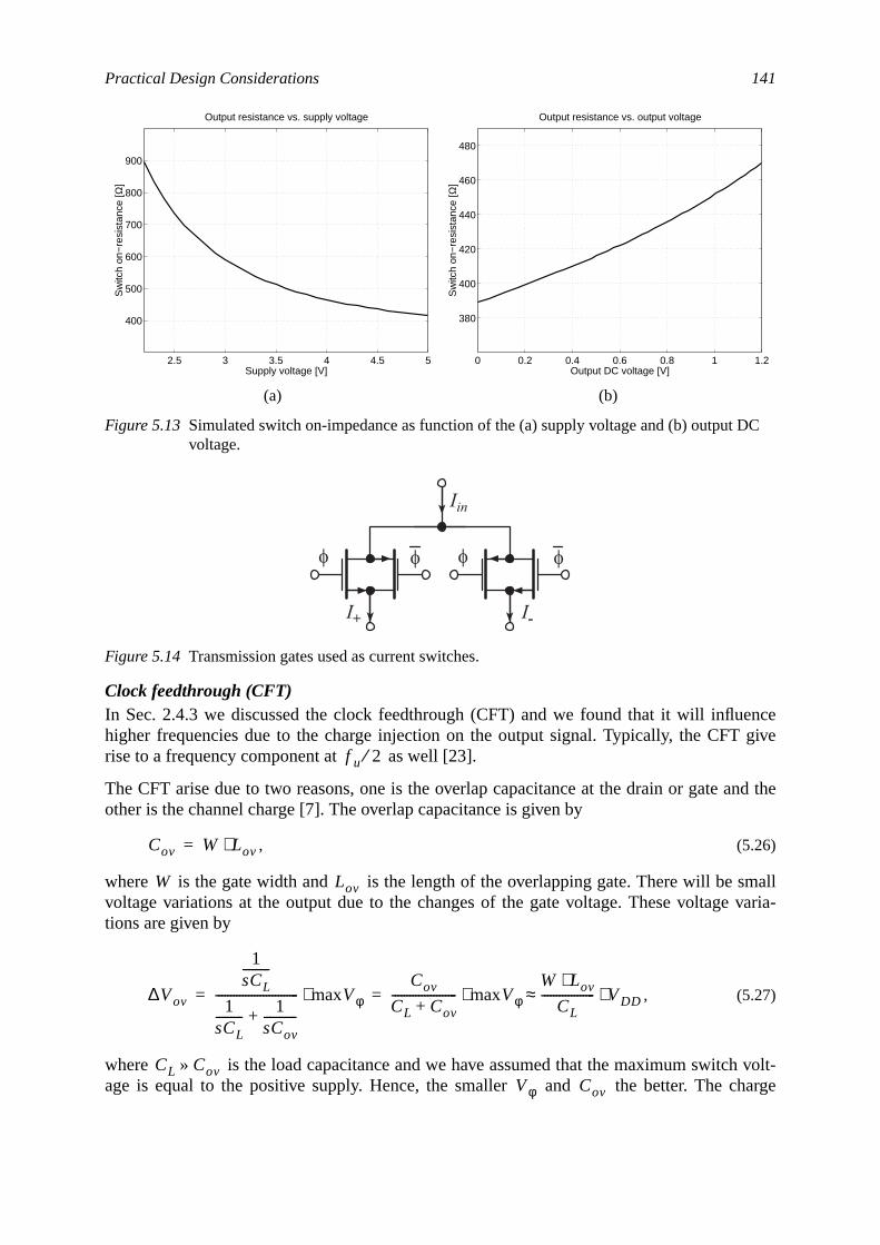
Practical Design Considerations 141
encegive
nd the
mallvaria-
volt-harge
DC
Clock feedthrough (CFT)In Sec. 2.4.3 we discussed the clock feedthrough (CFT) and we found that it will influhigher frequencies due to the charge injection on the output signal. Typically, the CFTrise to a frequency component at as well [23].
The CFT arise due to two reasons, one is the overlap capacitance at the drain or gate aother is the channel charge [7]. The overlap capacitance is given by
, (5.26)
where is the gate width and is the length of the overlapping gate. There will be svoltage variations at the output due to the changes of the gate voltage. These voltagetions are given by
, (5.27)
where is the load capacitance and we have assumed that the maximum switchage is equal to the positive supply. Hence, the smaller and the better. The c
(a) (b)
Figure 5.13 Simulated switch on-impedance as function of the (a) supply voltage and (b) output voltage.
Figure 5.14 Transmission gates used as current switches.
2.5 3 3.5 4 4.5 5
400
500
600
700
800
900
Supply voltage [V]
Sw
itch
on−
resi
stan
ce [Ω
]Output resistance vs. supply voltage
0 0.2 0.4 0.6 0.8 1 1.2
380
400
420
440
460
480
Output DC voltage [V]
Sw
itch
on−
resi
stan
ce [Ω
]
Output resistance vs. output voltage
I+ I-
f f
Iin
f f
f u 2⁄
Cov W Lov⋅=
W Lov
∆Vov
1sCL---------
1sCL--------- 1
sCov-----------+
---------------------------- maxVφ⋅Cov
CL Cov+---------------------- maxVφ⋅
W Lov⋅CL
------------------ VDD⋅≈= =
CL Cov»Vφ Cov
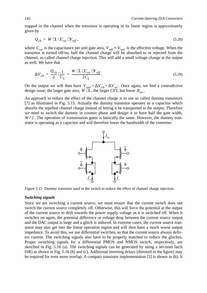
142 Current-Steering D/A Converters
ately
n thethe
utput
tive
sistorshichreforeidth,tran-
es nottput
en itoutpute tran-utputdeliv-tches.aret latchmayb). It
.
trapped in the channel when the transistor is operating in its linear region is approximgiven by
, (5.28)
where is the capacitance per unit gate area, is the effective voltage. Whetransistor is turned off/on, half the channel charge will be absorbed to or rejected fromchannel, so called channel charge injection. This will add a small voltage change at the oas well. We have that
. (5.29)
On the output we will then have . Once again, we find a contradicdesign issue; the larger gate area, , the larger CFT, but lower .
An approach to reduce the effect of the channel charge is to use so called dummy tran[7] as illustrated in Fig. 5.15. Actually the dummy transistor operates as a capacitor wabsorbs the repelled channel charge instead of letting it be transported to the output. Thewe need to switch the dummy in counter phase and design it to have half the gate w
. The operation of transmission gates is basically the same. However, the dummysistor is operating as a capacitor and will therefore lower the bandwidth of the converter.
Switching signalsSince we are switching a current source, we must ensure that the current switch doswitch the current source completely off. Otherwise, this will force the potential at the ouof the current source to drift towards the power supply voltage as it is switched off. Whswitches on again, the potential difference or voltage drop between the current sourceand the DAC output is large and a glitch is induced. In extreme cases, the current sourcsistor may also get into the linear operation region and will then have a much worse oimpedance. To avoid this, we use differential switches, so that the current source alwaysers current. The switching signals also have to be properly matched to reduce the gliProper switching signals for a differential PMOS and NMOS switch, respectively,sketched in Fig. 5.16 (a). The switching signals can be generated by using a set-rese(SR) as shown in Fig. 5.16 (b) and (c). Additional inverting delays (dimmed in the figure)be required for even more overlap. A compact transistor implementation [5] is shown in (
Figure 5.15 Dummy transistor used in the switch to reduce the effect of channel charge injection
Qch W L⋅ Cox Veff⋅ ⋅=
Cox Veff Vout≈
∆Vch
Qch
2--------- 1
CL------⋅
W L⋅ Cox Veff⋅ ⋅2CL
-----------------------------------------= =
Vout ∆Vch ∆Vov+ +W L⋅ Rsw
W 2⁄
I+
Iin
I-
f f
ff
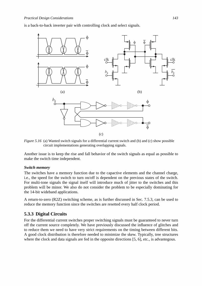
Practical Design Considerations 143
ible to
harge,witch.thisg for
sed to
r turns andt bits.uresgous.
ble
is a back-to-back inverter pair with controlling clock and select signals.
Another issue is to keep the rise and fall behavior of the switch signals as equal as possmake the switch time independent.
Switch memoryThe switches have a memory function due to the capactive elements and the channel ci.e., the speed for the switch to turn on/off is dependent on the previous states of the sFor multi-tone signals the signal itself will introduce much of jitter to the switches andproblem will be minor. We also do not consider the problem to be especially dominatinthe 14-bit wideband applications.
A return-to-zero (R2Z) switching scheme, as is further discussed in Sec. 7.5.3, can be ureduce the memory function since the switches are resetted every half clock period.
5.3.3 Digital CircuitsFor the differential current switches proper switching signals must be guaranteed to neveoff the current source completely. We have previously discussed the influence of glitcheto reduce them we need to have very strict requirements on the timing between differenA good clock distribution is therefore needed to minimize the skew. Typically, tree structwhere the clock and data signals are fed in the opposite directions [5, 6], etc., is advante
(a) (b)
(c)
Figure 5.16 (a) Wanted switch signals for a differential current switch and (b) and (c) show possicircuit implementations generating overlapping signals.
f
f
f
fclkclk
bk
f f
bk
bk f
f
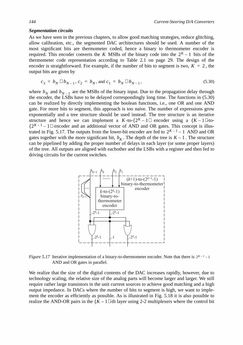
144 Current-Steering D/A Converters
tching,f the
der isf theof the, the
ough(5.30)AND
growerative-to-
llus-ORctureayers)fed to
ue toe stilla highple-le to
l bit
Segmentation circuitsAs we have seen in the previous chapters, to allow good matching strategies, reduce gliallow calibration, etc., the segmented DAC architectures should be used. A number omost significant bits are thermometer coded, hence a binary to thermometer encorequired. This encoder converts the MSBs of the binary code into the bits othermometer code representation according to Table 2.1 on page 29. The designencoder is straightforward. For example, if the number of bits to segment is two,output bits are given by
, , and , (5.30)
where and are the MSBs of the binary input. Due to the propagation delay thrthe encoder, the LSBs have to be delayed correspondingly long time. The functions incan be realized by directly implementing the boolean functions, i.e., one OR and onegate. For more bits to segment, this approach is too naive. The number of expressionsexponentially and a tree structure should be used instead. The tree structure is an itstructure and hence we can implement a -to- encoder using a
encoder and an additional vector of AND and OR gates. This concept is itrated in Fig. 5.17. The outputs from the lower-bit encoder are fed to AND andgates together with the more significant bit, . The depth of the tree is . The strucan be pipelined by adding the proper number of delays in each layer (or some proper lof the tree. All outputs are aligned with eachother and the LSBs with a register and thendriving circuits for the current switches.
We realize that the size of the digital contents of the DAC increases rapidly, however, dtechnology scaling, the relative size of the analog parts will become larger and larger. Wrequire rather large transistors in the unit current sources to achieve good matching andoutput impedance. In DACs where the number of bits to segment is high, we want to imment the encoder as efficiently as possible. As is illustrated in Fig. 5.18 it is also possibrealize the AND-OR pairs in the -th layer using 2-2 multiplexers where the contro
Figure 5.17 Iterative implementation of a binary-to-thermometer encoder. Note that there isAND and OR gates in parallel.
K 2K 1–
K 2=
c3 bN bN 1–∧= c2 bN= c1 bN bN 1–∨=
bN bN 1–
K 2K 1–( ) K 1–( )2K 1– 1–( )
2K 1– 1–bK K 1–
(k+1)-to-(2k+1-1)binary-to-thermometer
encoderk-to-(2k-1)binary-to-
thermometerencoder
bk+1
2k-12k-1
2k-12k-1 1
b1bk b2
bk+1
2K 1– 1–
K 1–( )
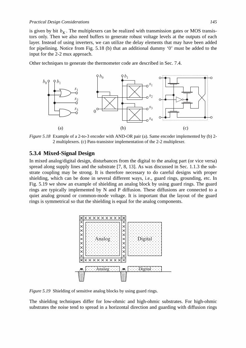
Practical Design Considerations 145
nsis-f eachaddedthe
ersa)e sub-ropertc. Inguardto a
uard
micrings
b) 2-
is given by bit . The multiplexers can be realized with transmission gates or MOS trators only. Then we also need buffers to generate robust voltage levels at the outputs olayer. Instead of using inverters, we can utilize the delay elements that may have beenfor pipelining. Notice from Fig. 5.18 (b) that an additional dummy ‘0’ must be added toinput for the 2-2 mux approach.
Other techniques to generate the thermometer code are described in Sec. 7.4.
5.3.4 Mixed-Signal DesignIn mixed analog/digital design, disturbances from the digital to the analog part (or vice vspread along supply lines and the substrate [7, 8, 13]. As was discussed in Sec. 1.1.3 thstrate coupling may be strong. It is therefore necessary to do careful designs with pshielding, which can be done in several different ways, i.e., guard rings, grounding, eFig. 5.19 we show an example of shielding an analog block by using guard rings. Therings are typically implemented by N and P diffusion. These diffusions are connectedquiet analog ground or common-mode voltage. It is important that the layout of the grings is symmetrical so that the shielding is equal for the analog components.
The shielding techniques differ for low-ohmic and high-ohmic substrates. For high-ohsubstrates the noise tend to spread in a horizontal direction and guarding with diffusion
(a) (b) (c)
Figure 5.18 Example of a 2-to-3 encoder with AND-OR pair (a). Same encoder implemented by (2 multiplexers. (c) Pass-transistor implementation of the 2-2 multiplexer.
Figure 5.19 Shielding of sensitive analog blocks by using guard rings.
bK
b0 b1
s1
s2
s3 0
b0 b1
s2
s1
s3
s4
Analog Digital
Analog Digital
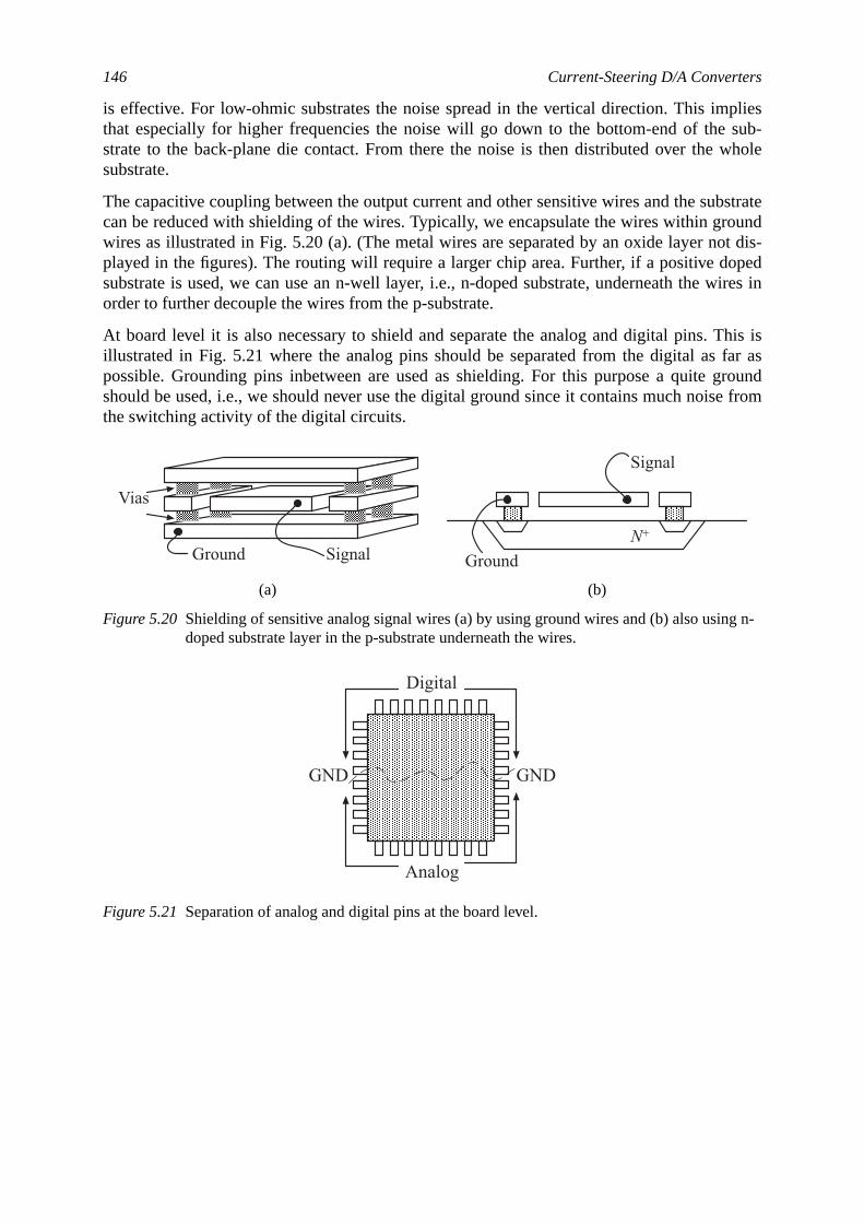
146 Current-Steering D/A Converters
pliessub-whole
bstrateoundt dis-pedires in
his isfar asround
e from
g n-
is effective. For low-ohmic substrates the noise spread in the vertical direction. This imthat especially for higher frequencies the noise will go down to the bottom-end of thestrate to the back-plane die contact. From there the noise is then distributed over thesubstrate.
The capacitive coupling between the output current and other sensitive wires and the sucan be reduced with shielding of the wires. Typically, we encapsulate the wires within grwires as illustrated in Fig. 5.20 (a). (The metal wires are separated by an oxide layer noplayed in the figures). The routing will require a larger chip area. Further, if a positive dosubstrate is used, we can use an n-well layer, i.e., n-doped substrate, underneath the worder to further decouple the wires from the p-substrate.
At board level it is also necessary to shield and separate the analog and digital pins. Tillustrated in Fig. 5.21 where the analog pins should be separated from the digital aspossible. Grounding pins inbetween are used as shielding. For this purpose a quite gshould be used, i.e., we should never use the digital ground since it contains much noisthe switching activity of the digital circuits.
(a) (b)
Figure 5.20 Shielding of sensitive analog signal wires (a) by using ground wires and (b) also usindoped substrate layer in the p-substrate underneath the wires.
Figure 5.21 Separation of analog and digital pins at the board level.
Signal
Vias
Ground GroundN+
Signal
Digital
Analog
GNDGND
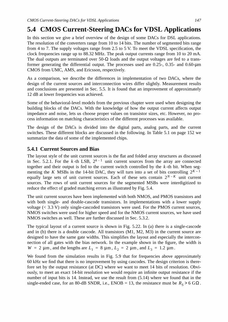
CMOS Current-Steering DACs for VDSL Applications 147
ns.range, the
mA.s-
60-
theesults
ately
ng thetputno pro-
rrent2 we
ussedctedseg-
rrented to
rs andpplyurces,e used
codeare
ercon-th is
atelythere-Obvi-if then the
.
5.4 CMOS Current-Steering DACs for VDSL ApplicationsIn this section we give a brief overview of the design of some DACs for DSL applicatioThe resolution of the converters range from 10 to 14 bits. The number of segmented bitsfrom 4 to 7. The supply voltages range from 2.5 to 5 V. To meet the VDSL specificationclock frequencies range up to 88.32 MHz. The peak output currents range from 10 to 20The dual outputs are terminated over 50-Ω loads and the output voltages are fed to a tranformer generating the differential output. The processes used are 0.25-, 0.35- and 0.µmCMOS from UMC, AMS, and Ericsson, respectively.
As a comparison, we describe the differences in implementation of two DACs, wheredesign of the current sources and interconnection wires differ slightly. Measurement rand conclusions are presented in Sec. 5.5. It is found that an improvement of approxim12 dB at lower frequencies was achieved.
Some of the behavioral-level models from the previous chapter were used when designibuilding blocks of the DACs. With the knowledge of how the output current affects ouimpedance and noise, lets us choose proper values on transistor sizes, etc. However,cess information on matching characteristics of the different processes was available.
The design of the DACs is divided into the digital parts, analog parts, and the cuswitches. These different blocks are discussed in the following. In Table 5.1 on page 15summarize the data of some of the implemented chips.
5.4.1 Current Sources and BiasThe layout style of the unit current sources is the flat and folded array structures as discin Sec. 5.2.1. For the -th LSB, unit current sources from the array are connetogether and their output is fed to the current switch controlled by the -th bit. Whenmenting the MSBs in the 14-bit DAC, they will turn into a set of bits controllingequally large sets of unit current sources. Each of these sets contain unit cusources. The rows of unit current sources for the segmented MSBs were interdigitizreduce the effect of graded matching errors as illustrated by Fig. 5.4.
The unit current sources have been implemented with both NMOS, and PMOS transistowith both single- and double-cascode transistors. In implementations with a lower suvoltage (< 3.3 V) only single-cascoded transistors were used. For the PMOS current soNMOS switches were used for higher speed and for the NMOS current sources, we havNMOS switches as well. These are further discussed in Sec. 5.3.2.
The typical layout of a current source is shown in Fig. 5.22. In (a) there is a single-casand in (b) there is a double cascode. All transistors (M1, M2, M3) in the current sourcedesigned to have the same gate widths. This simplifies the layout and especially the intnection of all gates with the bias network. In the example shown in the figure, the wid
, and the lengths are , , and .
We found from the simulation results in Fig. 5.9 that for frequencies above approxim60 kHz we find that there is no improvement by using cascodes. The design criterion isfore set by the output resistance (at DC) where we want to meet 14 bits of resolution.ously, to meet an exact 14-bit resolution we would require an infinite output resistancenumber of input bits is 14. Instead, we use the result from (5.14) where we found that isingle-ended case, for an 80-dB SNDR, i.e., ENOB = 13, the resistance must be
k 2k 1–
kK 2K 1–
2N K–
W 2 µm= L1 8 µm= L2 2 µm= L3 1.2 µm=
RS 6 GΩ>
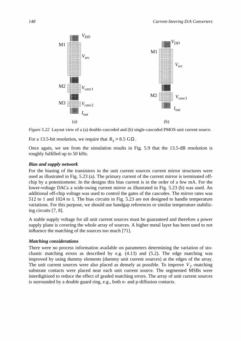
148 Current-Steering D/A Converters
on is
wereoff-
r the. Ans wasraturetabiliz-
powerto not
f sto-g wasarray.tchings wereurces
urce.
For a 13.5-bit resolution, we require that .
Once again, we see from the simulation results in Fig. 5.9 that the 13.5-dB resolutiroughly fulfilled up to 50 kHz.
Bias and supply networkFor the biasing of the transistors in the unit current sources current mirror structuresused as illustrated in Fig. 5.23 (a). The primary current of the current mirror is terminatedchip by a potentiometer. In the designs this bias current is in the order of a few mA. Folower-voltage DACs a wide-swing current mirror as illustrated in Fig. 5.23 (b) was usedadditional off-chip voltage was used to control the gates of the cascodes. The mirror rate512 to 1 and 1024 to 1. The bias circuits in Fig. 5.23 are not designed to handle tempevariations. For this purpose, we should use bandgap references or similar temperature sing circuits [7, 8].
A stable supply voltage for all unit current sources must be guaranteed and therefore asupply plane is covering the whole array of sources. A higher metal layer has been usedinfluence the matching of the sources too much [71].
Matching considerationsThere were no process information available on parameters determining the variation ochastic matching errors as described by e.g. (4.13) and (5.2). The edge matchinimproved by using dummy elements (dummy unit current sources) at the edges of theThe unit current sources were also placed as densely as possible. To improve -masubstrate contacts were placed near each unit current source. The segmented MSBinterdigitized to reduce the effect of graded matching errors. The array of unit current sois surrounded by a double guard ring, e.g., both n- and p-diffusion contacts.
(a) (b)
Figure 5.22 Layout view of a (a) double-cascoded and (b) single-cascoded PMOS unit current so
M1
M2
M3
VDD
Iout
Vsrc
Vcasc1
Vcasc2
M1
M2
VDD
Iout
Vsrc
Vcasc1
RS 8.5 GΩ>
VT
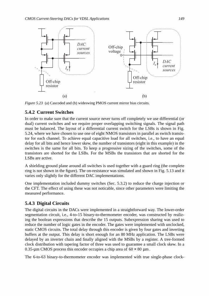
CMOS Current-Steering DACs for VDSL Applications 149
ial (orl pathFig.ansis-equalin theof theor the
pleteand it
ion org the
rderealiz-used toocked,rting
weremed. In a
lock-
5.4.2 Current SwitchesIn order to make sure that the current source never turns off completely we use differentdual) current switches and we require proper overlapping switching signals. The signamust be balanced. The layout of a differential current switch for the LSBs is shown in5.24, where we have chosen to use one of eight NMOS transistors in parallel as switch trtor for each channel. To achieve equal capacitive load for all switches, i.e., to have andelay for all bits and hence lower skew, the number of transistors (eight in this example)switches is the same for all bits. To keep a progressive sizing of the switches, sometransistors are shorted for the LSBs. For the MSBs the transistors that are shorted fLSBs are active.
A shielding ground plane around all switches is used together with a guard ring (the comring is not shown in the figure). The on-resistance was simulated and shown in Fig. 5.13varies only slightly for the different DAC implementations.
One implementation included dummy switches (Sec. 5.3.2) to reduce the charge injectthe CFT. The effect of using these was not noticable, since other parameters were limitinmeasured performance.
5.4.3 Digital CircuitsThe digital circuits in the DACs were implemented in a straightforward way. The lower-osegmentation circuit, i.e., 4-to-15 binary-to-thermometer encoder, was constructed by ring the boolean expressions that describe the 15 outputs. Subexpression sharing wasreduce the number of logic gates in the encoder. The gates were implemented with unclstatic CMOS circuits. The total delay through this encoder is given by four gates and invebuffers at the output. This delay is short enough for an 80 MHz application. The LSBsdelayed by an inverter chain and finally aligned with the MSBs by a register. A tree-forclock distribution with tapering factor of three was used to guarantee a small clock skew0.35-µm CMOS process this encoder occupies a chip area of .
The 6-to-63 binary-to-thermometer encoder was implemented with true single-phase c
,
(a) (b)
Figure 5.23 (a) Cascoded and (b) wideswing PMOS current mirror bias circuits.
Off-chipresistor
Iu
DACcurrentsources
Off-chipresistor
IuDACcurrentsources
Off-chipvoltage
60 80µm×
150 Current-Steering D/A Converters
-
6 (c).oppo-
pho-chip
enta-Then
. 5.26ary-
e unitasuredsed in
marizedlated,fromTwo
mea-
ing (TSPC) logic. The tree was pipelined to ensure a high clock frequency. In a 0.25µmCMOS process, this encoder occupies a chip area of mm2.
The circuits generating overlapping switch signals had a structure as shown in Fig. 5.1For PMOS switches we replace the NAND gates with NOR gates to compensate for thesite polarity.
5.4.4 Chip ImplementationsThe layouts of the DACs are all similar with some exceptions. In Fig. 5.25 we show a dietograph of one of the chips (This is DAC A in Table 5.1). Since it was designed as a testthe digital circuits were placed apart from the unit current source array. A better implemtion would be to rotate the digital circuits and put the closer to the current source array.we get much shorter interconnection wires which reduces the parasitic resistance.
These types of changes were done in some of the other DACs as the example in Figshows. (This is DAC E in Table 5.1). It has a larger digital contents due to the 6-to-63 binto-thermometer encoding circuit.
In Table 5.1 we summarize some of the implemented Nyquist-rate DACs. The data on thcurrent sources and the switches is also included in the table. Further, we find the meSFDR for some different signal and clock frequencies. More on these results is discusthe following section.
5.5 Measurement ResultsIn this section some measured results are shown and concluded. Some results are sumin Table 5.1 on page 152. A comparison study is also given where the measured, simuand calculated results are compared. DAC A and B are of the same generation. DAC C isthe second generation, DAC D third generation, and DAC E is the fourth generation.DACs of different generations, DAC A/B and C, are compared and the improvement insured SFDR is discussed.
Figure 5.24 Layout view of a differential current switch for the LSBs.
Ground
Iout+
Iout–
Iin
φ
φ
1.1 0.165×
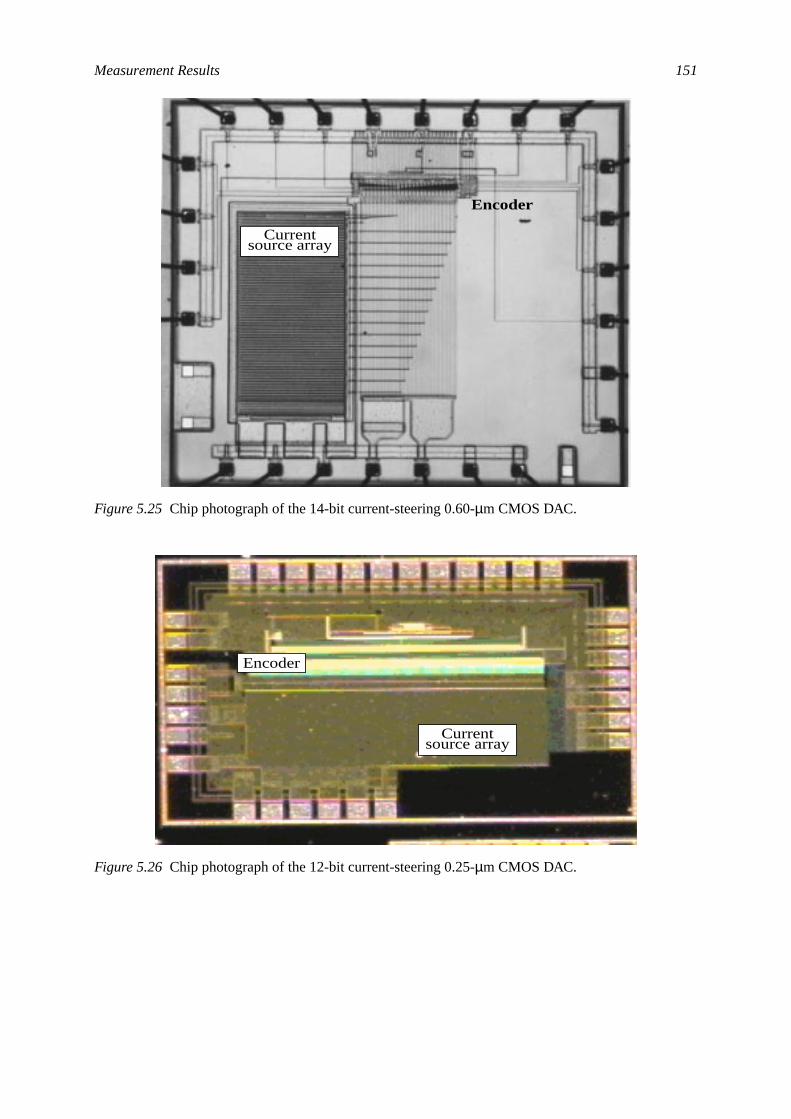
Measurement Results 151
Figure 5.25 Chip photograph of the 14-bit current-steering 0.60-µm CMOS DAC.
Figure 5.26 Chip photograph of the 12-bit current-steering 0.25-µm CMOS DAC.
Encoder
Currentsource array
Currentsource array
Encoder
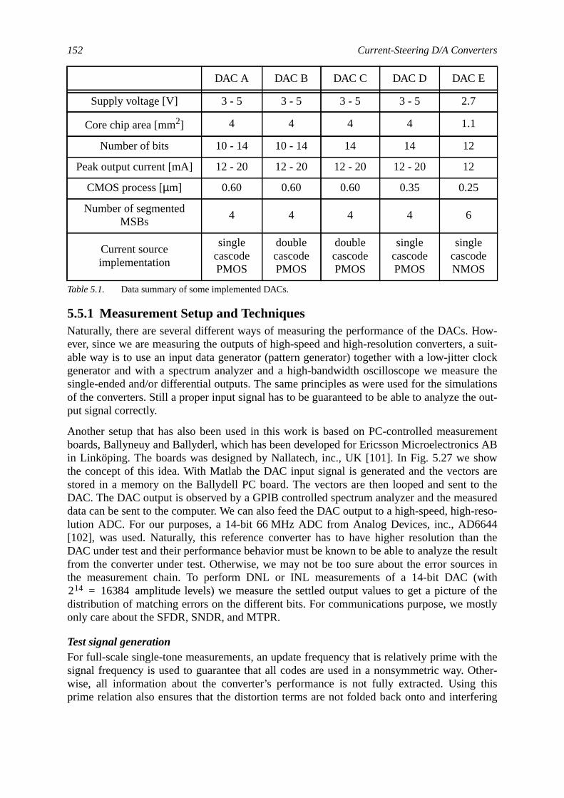
152 Current-Steering D/A Converters
How-a suit-clockre the
lationse out-
rements ABhows areto thesuredh-reso-44n theresultces inwithf theostly
th theOther-thisfering
5.5.1 Measurement Setup and TechniquesNaturally, there are several different ways of measuring the performance of the DACs.ever, since we are measuring the outputs of high-speed and high-resolution converters,able way is to use an input data generator (pattern generator) together with a low-jittergenerator and with a spectrum analyzer and a high-bandwidth oscilloscope we measusingle-ended and/or differential outputs. The same principles as were used for the simuof the converters. Still a proper input signal has to be guaranteed to be able to analyze thput signal correctly.
Another setup that has also been used in this work is based on PC-controlled measuboards, Ballyneuy and Ballyderl, which has been developed for Ericsson Microelectronicin Linköping. The boards was designed by Nallatech, inc., UK [101]. In Fig. 5.27 we sthe concept of this idea. With Matlab the DAC input signal is generated and the vectorstored in a memory on the Ballydell PC board. The vectors are then looped and sentDAC. The DAC output is observed by a GPIB controlled spectrum analyzer and the meadata can be sent to the computer. We can also feed the DAC output to a high-speed, higlution ADC. For our purposes, a 14-bit 66 MHz ADC from Analog Devices, inc., AD66[102], was used. Naturally, this reference converter has to have higher resolution thaDAC under test and their performance behavior must be known to be able to analyze thefrom the converter under test. Otherwise, we may not be too sure about the error sourthe measurement chain. To perform DNL or INL measurements of a 14-bit DAC (
amplitude levels) we measure the settled output values to get a picture odistribution of matching errors on the different bits. For communications purpose, we monly care about the SFDR, SNDR, and MTPR.
Test signal generationFor full-scale single-tone measurements, an update frequency that is relatively prime wisignal frequency is used to guarantee that all codes are used in a nonsymmetric way.wise, all information about the converter’s performance is not fully extracted. Usingprime relation also ensures that the distortion terms are not folded back onto and inter
DAC A DAC B DAC C DAC D DAC E
Supply voltage [V] 3 - 5 3 - 5 3 - 5 3 - 5 2.7
Core chip area [mm2] 4 4 4 4 1.1
Number of bits 10 - 14 10 - 14 14 14 12
Peak output current [mA] 12 - 20 12 - 20 12 - 20 12 - 20 12
CMOS process [µm] 0.60 0.60 0.60 0.35 0.25
Number of segmentedMSBs
4 4 4 4 6
Current sourceimplementation
singlecascodePMOS
doublecascodePMOS
doublecascodePMOS
singlecascodePMOS
singlecascodeNMOS
Table 5.1. Data summary of some implemented DACs.
214 16384=
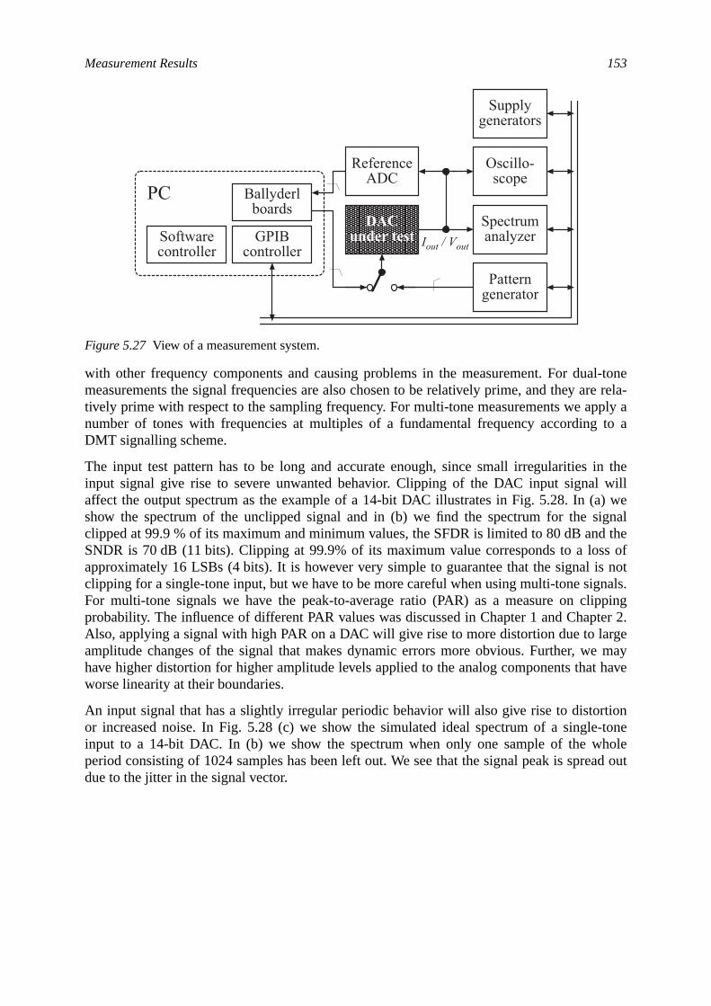
Measurement Results 153
l-tonere rela-ply ato a
in thewill) weignalthe
s ofs notnals.ippingter 2.rge
mayt have
tion-tone
holead out
with other frequency components and causing problems in the measurement. For duameasurements the signal frequencies are also chosen to be relatively prime, and they atively prime with respect to the sampling frequency. For multi-tone measurements we apnumber of tones with frequencies at multiples of a fundamental frequency accordingDMT signalling scheme.
The input test pattern has to be long and accurate enough, since small irregularitiesinput signal give rise to severe unwanted behavior. Clipping of the DAC input signalaffect the output spectrum as the example of a 14-bit DAC illustrates in Fig. 5.28. In (ashow the spectrum of the unclipped signal and in (b) we find the spectrum for the sclipped at 99.9 % of its maximum and minimum values, the SFDR is limited to 80 dB andSNDR is 70 dB (11 bits). Clipping at 99.9% of its maximum value corresponds to a losapproximately 16 LSBs (4 bits). It is however very simple to guarantee that the signal iclipping for a single-tone input, but we have to be more careful when using multi-tone sigFor multi-tone signals we have the peak-to-average ratio (PAR) as a measure on clprobability. The influence of different PAR values was discussed in Chapter 1 and ChapAlso, applying a signal with high PAR on a DAC will give rise to more distortion due to laamplitude changes of the signal that makes dynamic errors more obvious. Further, wehave higher distortion for higher amplitude levels applied to the analog components thaworse linearity at their boundaries.
An input signal that has a slightly irregular periodic behavior will also give rise to distoror increased noise. In Fig. 5.28 (c) we show the simulated ideal spectrum of a singleinput to a 14-bit DAC. In (b) we show the spectrum when only one sample of the wperiod consisting of 1024 samples has been left out. We see that the signal peak is spredue to the jitter in the signal vector.
Figure 5.27 View of a measurement system.
Supplygenerators
Spectrumanalyzer
PC
ReferenceADC
GPIBcontroller
Ballyderlboards
Softwarecontroller
Oscillo-scope
Patterngenerator
Iout / Vout
DACunder test
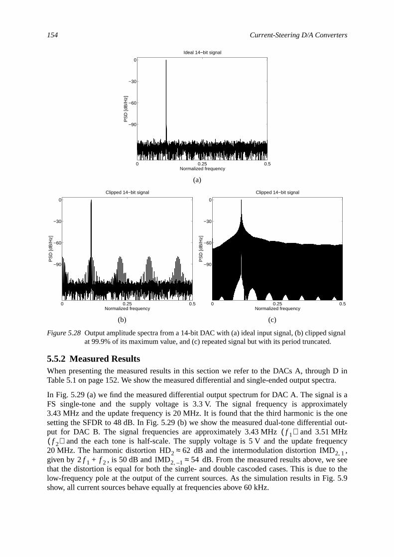
154 Current-Steering D/A Converters
D inctra.
is aatelyone
l out-Hzency,
seeto the. 5.9
nal.
5.5.2 Measured ResultsWhen presenting the measured results in this section we refer to the DACs A, throughTable 5.1 on page 152. We show the measured differential and single-ended output spe
In Fig. 5.29 (a) we find the measured differential output spectrum for DAC A. The signalFS single-tone and the supply voltage is 3.3 V. The signal frequency is approxim3.43 MHz and the update frequency is 20 MHz. It is found that the third harmonic is thesetting the SFDR to 48 dB. In Fig. 5.29 (b) we show the measured dual-tone differentiaput for DAC B. The signal frequencies are approximately 3.43 MHz and 3.51 M
and the each tone is half-scale. The supply voltage is 5 V and the update frequ20 MHz. The harmonic distortion dB and the intermodulation distortiongiven by , is 50 dB and dB. From the measured results above, wethat the distortion is equal for both the single- and double cascoded cases. This is duelow-frequency pole at the output of the current sources. As the simulation results in Figshow, all current sources behave equally at frequencies above 60 kHz.
(a)
(b) (c)
Figure 5.28 Output amplitude spectra from a 14-bit DAC with (a) ideal input signal, (b) clipped sigat 99.9% of its maximum value, and (c) repeated signal but with its period truncated
0 0.25 0.5
−90
−60
−30
0
Normalized frequency
PS
D [d
B/H
z]
Ideal 14−bit signal
0 0.25 0.5
−90
−60
−30
0
Normalized frequency
PS
D [d
B/H
z]
Clipped 14−bit signal
0 0.25 0.5
−90
−60
−30
0
Normalized frequency
PS
D [d
B/H
z]
Clipped 14−bit signal
f 1( )f 2( )
HD2 62≈ IMD 2 1,2 f 1 f 2+ IMD 2 1–, 54≈
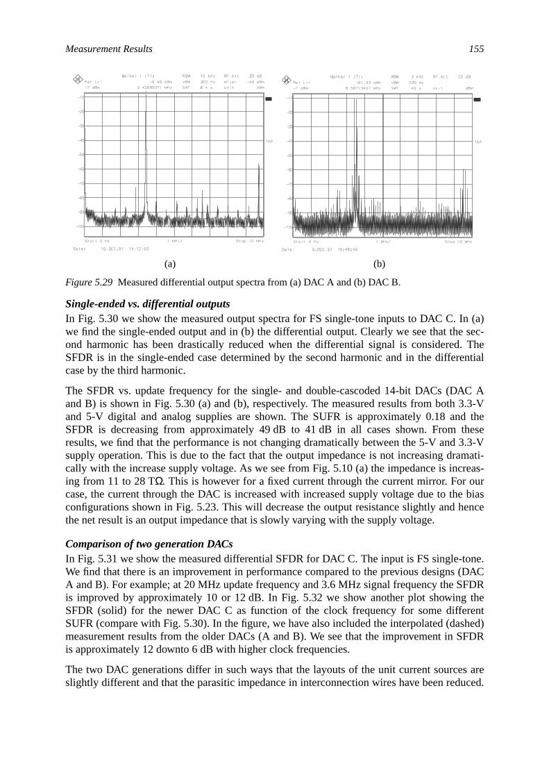
Measurement Results 155
In (a)sec-
. Therential
C A3.3-Vd thehese3.3-Vmati-reas-ure biasence
one.(DACFDRthe
entshed)FDR
s areuced.
Single-ended vs. differential outputsIn Fig. 5.30 we show the measured output spectra for FS single-tone inputs to DAC C.we find the single-ended output and in (b) the differential output. Clearly we see that theond harmonic has been drastically reduced when the differential signal is consideredSFDR is in the single-ended case determined by the second harmonic and in the diffecase by the third harmonic.
The SFDR vs. update frequency for the single- and double-cascoded 14-bit DACs (DAand B) is shown in Fig. 5.30 (a) and (b), respectively. The measured results from bothand 5-V digital and analog supplies are shown. The SUFR is approximately 0.18 anSFDR is decreasing from approximately 49 dB to 41 dB in all cases shown. From tresults, we find that the performance is not changing dramatically between the 5-V andsupply operation. This is due to the fact that the output impedance is not increasing dracally with the increase supply voltage. As we see from Fig. 5.10 (a) the impedance is incing from 11 to 28 TΩ. This is however for a fixed current through the current mirror. For ocase, the current through the DAC is increased with increased supply voltage due to thconfigurations shown in Fig. 5.23. This will decrease the output resistance slightly and hthe net result is an output impedance that is slowly varying with the supply voltage.
Comparison of two generation DACsIn Fig. 5.31 we show the measured differential SFDR for DAC C. The input is FS single-tWe find that there is an improvement in performance compared to the previous designsA and B). For example; at 20 MHz update frequency and 3.6 MHz signal frequency the Sis improved by approximately 10 or 12 dB. In Fig. 5.32 we show another plot showingSFDR (solid) for the newer DAC C as function of the clock frequency for some differSUFR (compare with Fig. 5.30). In the figure, we have also included the interpolated (dameasurement results from the older DACs (A and B). We see that the improvement in Sis approximately 12 downto 6 dB with higher clock frequencies.
The two DAC generations differ in such ways that the layouts of the unit current sourceslightly different and that the parasitic impedance in interconnection wires have been red
(a) (b)
Figure 5.29 Measured differential output spectra from (a) DAC A and (b) DAC B.
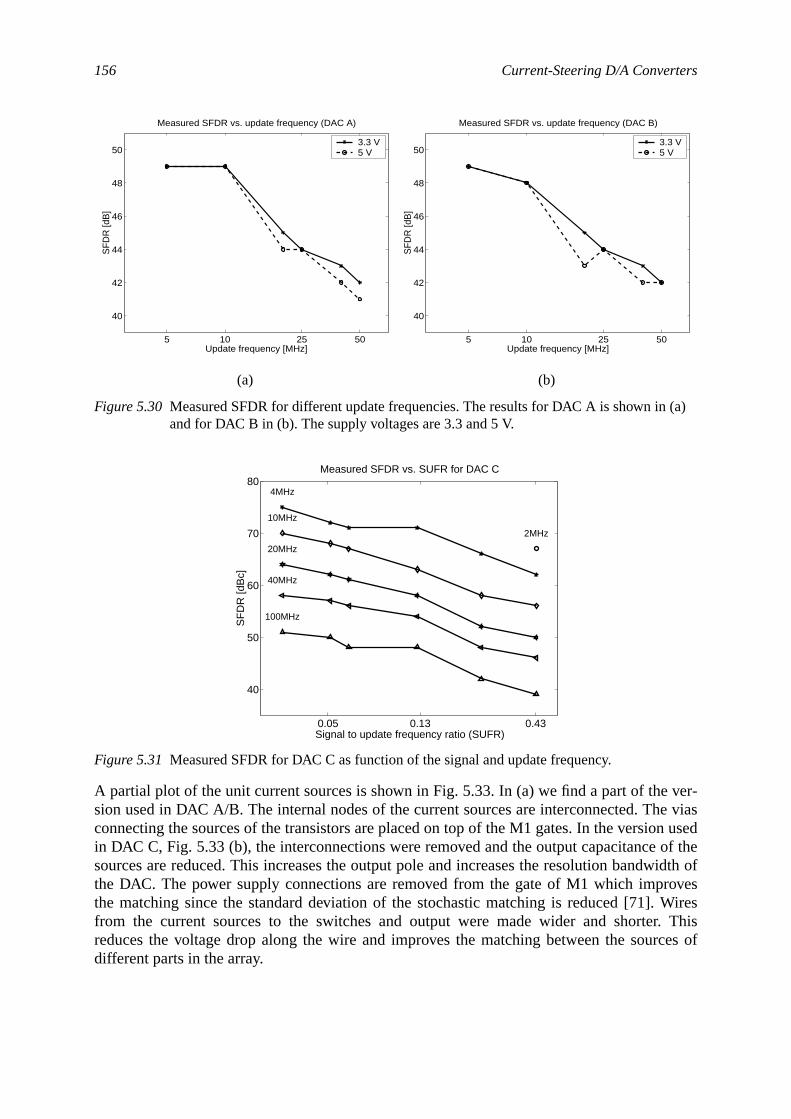
156 Current-Steering D/A Converters
ver-e viasn usedof the
idth ofovesWires. Thisces of
(a)
A partial plot of the unit current sources is shown in Fig. 5.33. In (a) we find a part of thesion used in DAC A/B. The internal nodes of the current sources are interconnected. Thconnecting the sources of the transistors are placed on top of the M1 gates. In the versioin DAC C, Fig. 5.33 (b), the interconnections were removed and the output capacitancesources are reduced. This increases the output pole and increases the resolution bandwthe DAC. The power supply connections are removed from the gate of M1 which imprthe matching since the standard deviation of the stochastic matching is reduced [71].from the current sources to the switches and output were made wider and shorterreduces the voltage drop along the wire and improves the matching between the sourdifferent parts in the array.
(a) (b)
Figure 5.30 Measured SFDR for different update frequencies. The results for DAC A is shown inand for DAC B in (b). The supply voltages are 3.3 and 5 V.
Figure 5.31 Measured SFDR for DAC C as function of the signal and update frequency.
5 10 25 50
40
42
44
46
48
50
Update frequency [MHz]
SF
DR
[dB
]
Measured SFDR vs. update frequency (DAC A)
3.3 V5 V
5 10 25 50
40
42
44
46
48
50
Update frequency [MHz]
SF
DR
[dB
]
Measured SFDR vs. update frequency (DAC B)
3.3 V5 V
0.05 0.13 0.43
40
50
60
70
804MHz
10MHz
20MHz
40MHz
100MHz
2MHz
Measured SFDR vs. SUFR for DAC C
Signal to update frequency ratio (SUFR)
SF
DR
[dB
c]
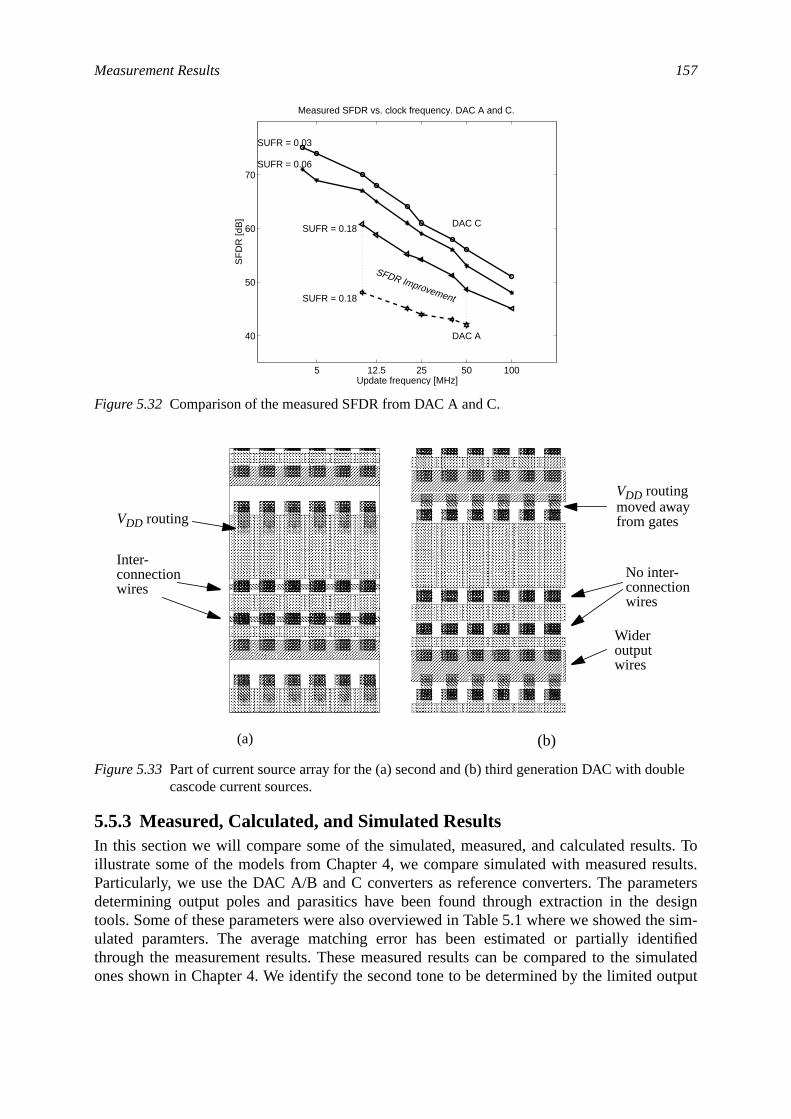
Measurement Results 157
lts. Tosults.eters
esigne sim-ntifiedmulatedutput
ble
5.5.3 Measured, Calculated, and Simulated ResultsIn this section we will compare some of the simulated, measured, and calculated resuillustrate some of the models from Chapter 4, we compare simulated with measured reParticularly, we use the DAC A/B and C converters as reference converters. The paramdetermining output poles and parasitics have been found through extraction in the dtools. Some of these parameters were also overviewed in Table 5.1 where we showed thulated paramters. The average matching error has been estimated or partially idethrough the measurement results. These measured results can be compared to the siones shown in Chapter 4. We identify the second tone to be determined by the limited o
Figure 5.32 Comparison of the measured SFDR from DAC A and C.
(a) (b)
Figure 5.33 Part of current source array for the (a) second and (b) third generation DAC with doucascode current sources.
5 12.5 25 50 100
40
50
60
70
SUFR = 0.03
SUFR = 0.06
SUFR = 0.18
DAC C
Measured SFDR vs. clock frequency. DAC A and C.
Update frequency [MHz]
SF
DR
[dB
]SUFR = 0.18
DAC A
SFDR Improvement
VDD routing
Inter-connectionwires
VDD routing
No inter-connectionwires
moved awayfrom gates
Wideroutputwires
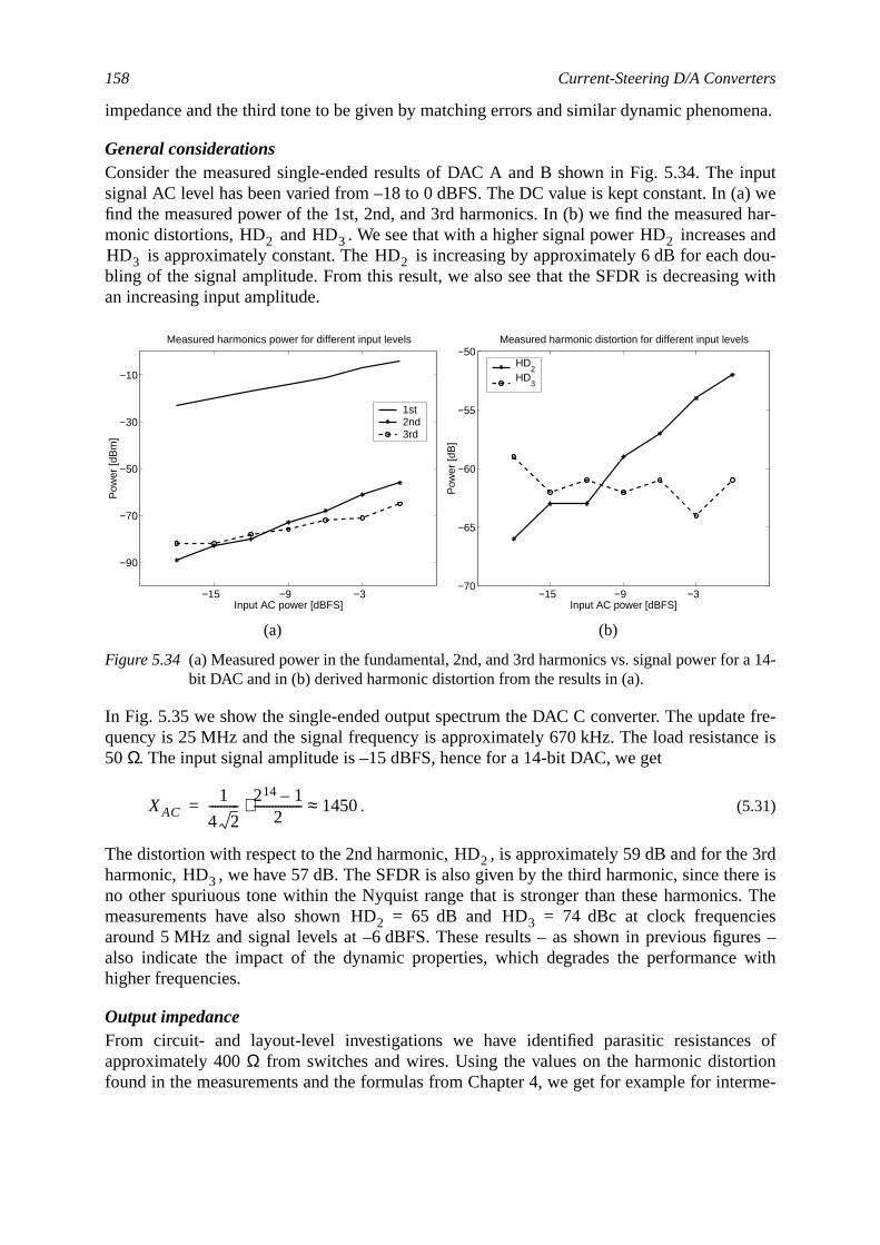
158 Current-Steering D/A Converters
mena.
input) wed har-and
dou-with
e fre-ce is
3rdre is. Theciesres –with
s oftionerme-
a 14-
impedance and the third tone to be given by matching errors and similar dynamic pheno
General considerationsConsider the measured single-ended results of DAC A and B shown in Fig. 5.34. Thesignal AC level has been varied from –18 to 0 dBFS. The DC value is kept constant. In (afind the measured power of the 1st, 2nd, and 3rd harmonics. In (b) we find the measuremonic distortions, and . We see that with a higher signal power increases
is approximately constant. The is increasing by approximately 6 dB for eachbling of the signal amplitude. From this result, we also see that the SFDR is decreasingan increasing input amplitude.
In Fig. 5.35 we show the single-ended output spectrum the DAC C converter. The updatquency is 25 MHz and the signal frequency is approximately 670 kHz. The load resistan50 Ω. The input signal amplitude is –15 dBFS, hence for a 14-bit DAC, we get
. (5.31)
The distortion with respect to the 2nd harmonic, , is approximately 59 dB and for theharmonic, , we have 57 dB. The SFDR is also given by the third harmonic, since theno other spuriuous tone within the Nyquist range that is stronger than these harmonicsmeasurements have also shown dB and dBc at clock frequenaround 5 MHz and signal levels at –6 dBFS. These results – as shown in previous figualso indicate the impact of the dynamic properties, which degrades the performancehigher frequencies.
Output impedanceFrom circuit- and layout-level investigations we have identified parasitic resistanceapproximately 400Ω from switches and wires. Using the values on the harmonic distorfound in the measurements and the formulas from Chapter 4, we get for example for int
(a) (b)
Figure 5.34 (a) Measured power in the fundamental, 2nd, and 3rd harmonics vs. signal power forbit DAC and in (b) derived harmonic distortion from the results in (a).
HD2 HD3 HD2HD3 HD2
−15 −9 −3
−90
−70
−50
−30
−10
Input AC power [dBFS]
Pow
er [d
Bm
]
Measured harmonics power for different input levels
1st2nd3rd
−15 −9 −3−70
−65
−60
−55
−50
Input AC power [dBFS]
Pow
er [d
B]
Measured harmonic distortion for different input levels
HD2
HD3
XAC1
4 2---------- 214 1–
2----------------⋅ 1450≈=
HD2HD3
HD2 65= HD3 74=
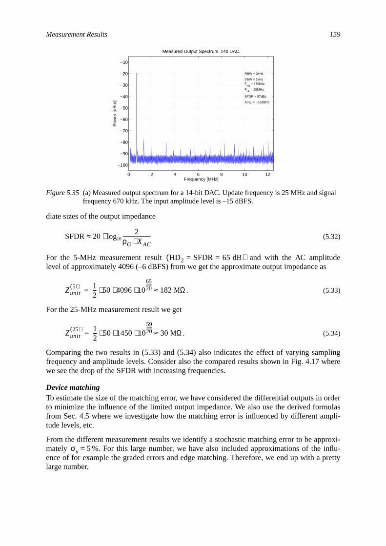
Measurement Results 159
des
plingwhere
orderulas
mpli-
proxi-nflu-pretty
nal
diate sizes of the output impedance
(5.32)
For the 5-MHz measurement result and with the AC amplitulevel of approximately 4096 (–6 dBFS) from we get the approximate output impedance a
. (5.33)
For the 25-MHz measurement result we get
. (5.34)
Comparing the two results in (5.33) and (5.34) also indicates the effect of varying samfrequency and amplitude levels. Consider also the compared results shown in Fig. 4.17we see the drop of the SFDR with increasing frequencies.
Device matchingTo estimate the size of the matching error, we have considered the differential outputs into minimize the influence of the limited output impedance. We also use the derived formfrom Sec. 4.5 where we investigate how the matching error is influenced by different atude levels, etc.
From the different measurement results we identify a stochastic matching error to be apmately %. For this large number, we have also included approximations of the ience of for example the graded errors and edge matching. Therefore, we end up with alarge number.
Figure 5.35 (a) Measured output spectrum for a 14-bit DAC. Update frequency is 25 MHz and sigfrequency 670 kHz. The input amplitude level is –15 dBFS.
0 2 4 6 8 10 12
−100
−90
−80
−70
−60
−50
−40
−30
−20
−10
Measured Output Spectrum. 14b DAC.
Frequency [MHz]
Pow
er [d
Bm
]
RBW = 3kHz
VBW = 1kHzF
sig = 670kHz
Fclk
= 25MHz
SFDR = 57dBc
Amp. = −15dBFS
SFDR 202
ρG XAC⋅---------------------log10⋅≈
HD2 SFDR 65 dB= =( )
Zunit5( ) 1
2--- 50 4096 10
6520------
⋅ ⋅ ⋅ 182MΩ≈=
Zunit25( ) 1
2--- 50 1450 10
5920------
⋅ ⋅ ⋅ 30 MΩ≈=
σu 5≈
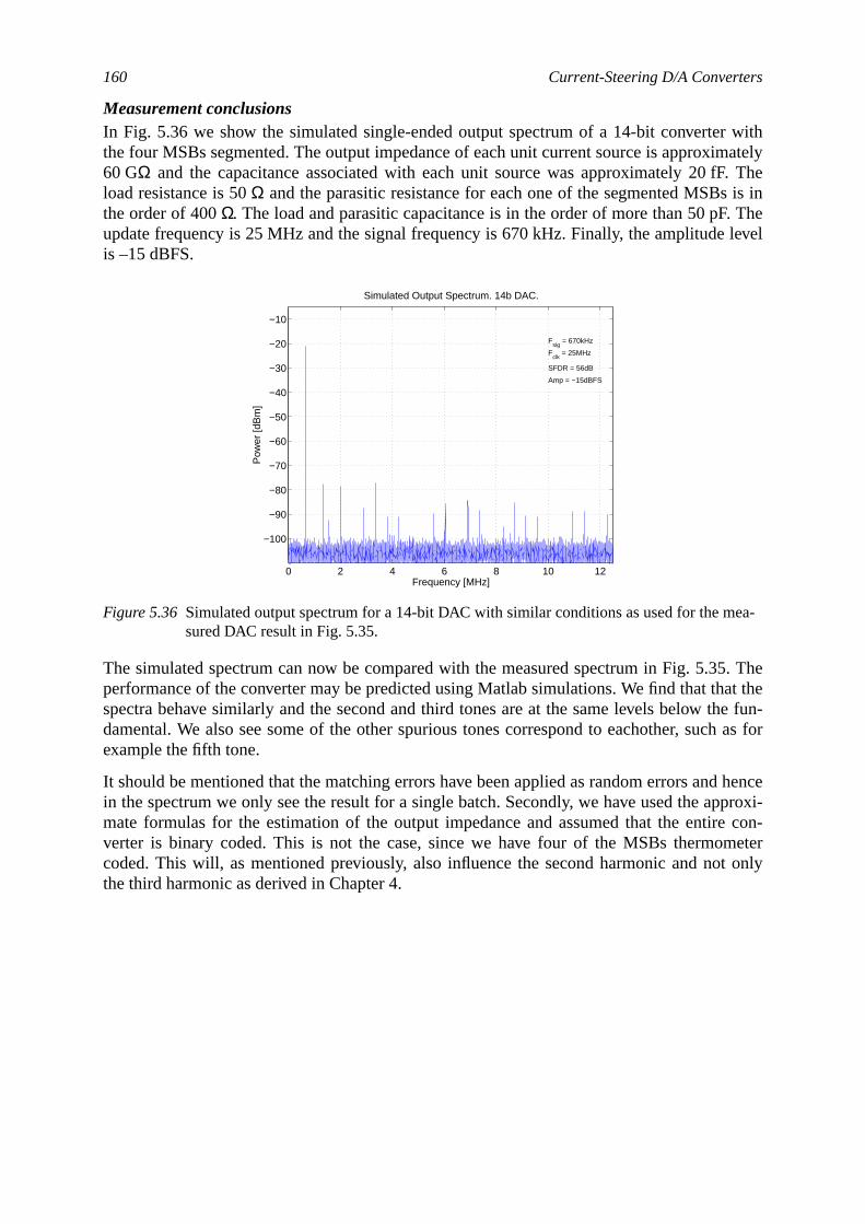
160 Current-Steering D/A Converters
withately
. Theis inThelevel
5. Theat thehe fun-h as for
henceproxi-
e con-metert only
ea-
Measurement conclusionsIn Fig. 5.36 we show the simulated single-ended output spectrum of a 14-bit converterthe four MSBs segmented. The output impedance of each unit current source is approxim60 GΩ and the capacitance associated with each unit source was approximately 20 fFload resistance is 50Ω and the parasitic resistance for each one of the segmented MSBsthe order of 400Ω. The load and parasitic capacitance is in the order of more than 50 pF.update frequency is 25 MHz and the signal frequency is 670 kHz. Finally, the amplitudeis –15 dBFS.
The simulated spectrum can now be compared with the measured spectrum in Fig. 5.3performance of the converter may be predicted using Matlab simulations. We find that thspectra behave similarly and the second and third tones are at the same levels below tdamental. We also see some of the other spurious tones correspond to eachother, sucexample the fifth tone.
It should be mentioned that the matching errors have been applied as random errors andin the spectrum we only see the result for a single batch. Secondly, we have used the apmate formulas for the estimation of the output impedance and assumed that the entirverter is binary coded. This is not the case, since we have four of the MSBs thermocoded. This will, as mentioned previously, also influence the second harmonic and nothe third harmonic as derived in Chapter 4.
Figure 5.36 Simulated output spectrum for a 14-bit DAC with similar conditions as used for the msured DAC result in Fig. 5.35.
0 2 4 6 8 10 12
−100
−90
−80
−70
−60
−50
−40
−30
−20
−10
Pow
er [d
Bm
]
Frequency [MHz]
Simulated Output Spectrum. 14b DAC.
Fsig
= 670kHz
Fclk
= 25MHz
SFDR = 56dB
Amp = −15dBFS
rredand-singere-cans can
er. WeDSLl cir-reasedcom-e cur-
ted inSec.D/A
ehav-ula-
pre-havethe
6 Oversampling D/AConverters
6.1 IntroductionThe oversampling D/A converter (OSDAC) is typically used when high linearity is prefeover high bandwidth. Traditionally, OSDACs are used in audio DACs since there the bwidth is relatively low and a high linearity is required [27, 29]. One of the advantages of uOSDACs is that the major part of the converter is implemented with digital circuits. Thfore, we can avoid many of the analog errors. With technology scaling the digital circuitsbe kept at a relatively small chip area and power consumption and hence the OSDACalso be used in applications were the bandwidth reaches the MHz range or even highcan allow oversampling ratios in the order of 32, 64, or even more for, for example, Aapplications where the signal bandwidth is approximately 1.104 MHz. Some of the digitacuits then have to operate at frequencies around 71 and 141 MHz, respectively. The incupdate frequency allows us to design the analog image-rejection filters with very lowplexity. Large requirements are however set on the switch signal generators and e.g. thrent switches due to the high sampling frequency.
The operation and properties of the oversampling converters in general were presenChapter 3. In Sec. 6.2 we take a somewhat closer look at the different building blocks. In6.3 we present the simulated behavior of some of the building blocks in the oversamplingconverter. We overview for example some filter orders and modulator orders and their bior. In Sec. 6.4 we describe a 3.3-V 14-bit current-steering OSDAC with a 5th-order modtor for DMT-ADSL.
6.2 OSDAC Building BlocksThe operation and use of the oversampling digital-to-analog converter (OSDAC) wassented in Chapter 3 and in Fig. 6.1 we repeat the block view of a general OSDAC. Wethe interpolator taking the input signal which is bandlimited to and increasesf N f u 2⁄=
161
162 Oversampling D/A Converters
.idealucesodula-(thelatorto
ts tos fromthise bitfilter
nals) is
oneslatione fre-func-ationlarge) we
it out-r fre-uous-screte-ed afil-
first-r we
us toted.rther,vary.d toband.nt of
tenua-
LP
update frequency by times, and we get the new update frequency ofThe interpolation filters attenuate images due to the interpolation operation and in thecase, they bandlimit the signal at the output of the interpolator to . The modulator redthe number of bits in the signal. Instead the signal is represented through pulse code mtion (PCM). The reduction of bits is done through truncation where the truncated bitstruncation error) or the modulator’s output is used in a feedback loop. The -bit moduoutput is fed to the DAC, which is a Nyquist-rate DAC with its input signal bandlimited
of the update frequency. With a lower-bit DAC, we have less analog componenlay out and special matching improvement techniques can be used since the parasiticinterconnection wires become smaller. If we have a one-bit modulator and incase, the DAC can be implemented by a so-called semi-digital FIR filter which takes thstream and lowpass filters it. Thereby, the requirements on the analog image-rejectioncan be significantly reduced.
In the frequency domain the power spectral density (PSD) of the internal OSDAC sigare illustrated by the example in Fig. 6.2 where the oversampling ratio (OSR
8 and the modulator order is 2. In (a) we show the input consisting of four –12 dBFS tand the whole bandwidth up to half the update frequency is used. Through interpothe update frequency is increased and a number of images is introduced in thquency domain as shown in (b). The interpolator is also designed to perform a filteringtion and in (c) we show the result using a 6th-order Cauer approximation as interpolfilter. The modulator truncates the input signal drastically and this operation introduces aamount of out-of-band noise (d) due to the highpass filtering of the truncation error. In (eshow the same result but with a logarithmic frequency axis. The modulator has a one-bput and therefore the high noise power. The (sub-) DAC that is operating at the highequency generates the output. This output should be filtered by an analog, contintime filter that attenuates the out-of-band noise and the images that arise due to the ditime operation of the DAC. Since the DAC is a one-bit DAC it can be cascaded and ussemi-digital FIR filter. In (f) we show the result when using a 19th-order semi-digital FIRter at the output.
From the example in Fig. 6.2 we see that the oversampling ratio is much too low for aorder, one-bit modulator since the noise shaping function is not powerful enough. Eithehave to increase the number of output bits from the modulator. This will however forceuse a multi-bit DAC and the semi-digital filtering function Fig. 6.2 (f) cannot be implemenIt is therefore better to increase the order of the modulator or the oversampling ratio. Fudependent on the order of the modulator the amount of out-of-band noise power willThis affects the filtering function of the continuous-time filter which then must be designehave a high stopband attenuation and with poor design even for a narrow transitionThen the complexity is too high since the purpose of the OSDAC is to reduce the amouanalog hardware. The same occurs if we use interpolation filters with poor stopband at
Figure 6.1 Generalized OSDAC architecture including interpolator, modulator, DAC, and analogfilter.
OSR f O u, OSR f u⋅=
f N
M
1 OSR⁄
M 1=
DAC LPSDIPFx(n) A(t)N M
X1 … X5, ,( )
f uOSR 1–( )
f O u,
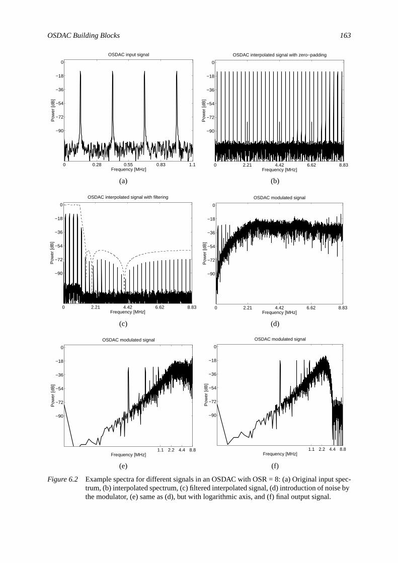
OSDAC Building Blocks 163
ec-by
(a) (b)
(c) (d)
(e) (f)
Figure 6.2 Example spectra for different signals in an OSDAC with OSR = 8: (a) Original input sptrum, (b) interpolated spectrum, (c) filtered interpolated signal, (d) introduction of noisethe modulator, (e) same as (d), but with logarithmic axis, and (f) final output signal.
0 0.28 0.55 0.83 1.1
−90
−72
−54
−36
−18
0
Frequency [MHz]
Pow
er [d
B]
OSDAC input signal
0 2.21 4.42 6.62 8.83
−90
−72
−54
−36
−18
0
Frequency [MHz]
Pow
er [d
B]
OSDAC interpolated signal with zero−padding
0 2.21 4.42 6.62 8.83
−90
−72
−54
−36
−18
0
Frequency [MHz]
Pow
er [d
B]
OSDAC interpolated signal with filtering
0 2.21 4.42 6.62 8.83
−90
−72
−54
−36
−18
0
Frequency [MHz]
Pow
er [d
B]
OSDAC modulated signal
1.1 2.2 4.4 8.8
−90
−72
−54
−36
−18
0
Frequency [MHz]
Pow
er [d
B]
OSDAC modulated signal
1.1 2.2 4.4 8.8
−90
−72
−54
−36
−18
0
Frequency [MHz]
Pow
er [d
B]
OSDAC modulated signal
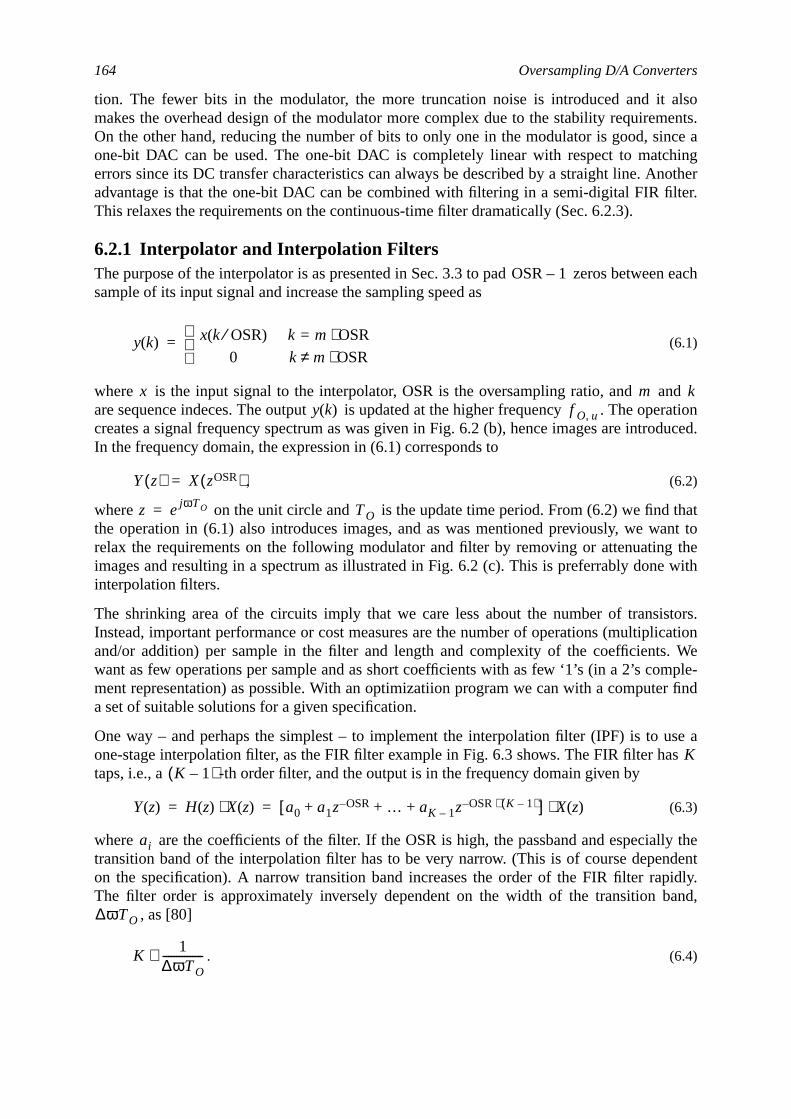
164 Oversampling D/A Converters
alsoents.
nce ahingnotherlter.
n each
ndrationduced.
thatant tothewith
stors.ication. Wemple-r find
se as
lly thedentidly.and,
tion. The fewer bits in the modulator, the more truncation noise is introduced and itmakes the overhead design of the modulator more complex due to the stability requiremOn the other hand, reducing the number of bits to only one in the modulator is good, sione-bit DAC can be used. The one-bit DAC is completely linear with respect to matcerrors since its DC transfer characteristics can always be described by a straight line. Aadvantage is that the one-bit DAC can be combined with filtering in a semi-digital FIR fiThis relaxes the requirements on the continuous-time filter dramatically (Sec. 6.2.3).
6.2.1 Interpolator and Interpolation FiltersThe purpose of the interpolator is as presented in Sec. 3.3 to pad zeros betweesample of its input signal and increase the sampling speed as
(6.1)
where is the input signal to the interpolator, OSR is the oversampling ratio, and aare sequence indeces. The output is updated at the higher frequency . The opecreates a signal frequency spectrum as was given in Fig. 6.2 (b), hence images are introIn the frequency domain, the expression in (6.1) corresponds to
, (6.2)
where on the unit circle and is the update time period. From (6.2) we findthe operation in (6.1) also introduces images, and as was mentioned previously, we wrelax the requirements on the following modulator and filter by removing or attenuatingimages and resulting in a spectrum as illustrated in Fig. 6.2 (c). This is preferrably doneinterpolation filters.
The shrinking area of the circuits imply that we care less about the number of transiInstead, important performance or cost measures are the number of operations (multipland/or addition) per sample in the filter and length and complexity of the coefficientswant as few operations per sample and as short coefficients with as few ‘1’s (in a 2’s coment representation) as possible. With an optimizatiion program we can with a computea set of suitable solutions for a given specification.
One way – and perhaps the simplest – to implement the interpolation filter (IPF) is to uone-stage interpolation filter, as the FIR filter example in Fig. 6.3 shows. The FIR filter hataps, i.e., a -th order filter, and the output is in the frequency domain given by
(6.3)
where are the coefficients of the filter. If the OSR is high, the passband and especiatransition band of the interpolation filter has to be very narrow. (This is of course depenon the specification). A narrow transition band increases the order of the FIR filter rapThe filter order is approximately inversely dependent on the width of the transition b
, as [80]
. (6.4)
OSR 1–
y k( ) x k OSR⁄( ) k m OSR⋅=
0 k m OSR⋅≠
=
x m ky k( ) f O u,
Y z( ) X zOSR( )=
z ejωTO= TO
KK 1–( )
Y z( ) H z( ) X z( )⋅ a0 a1z OSR– … aK 1– z OSR K 1–( )⋅–+ + +[ ] X z( )⋅= =
ai
∆ωTO
K1
∆ωTO---------------∼
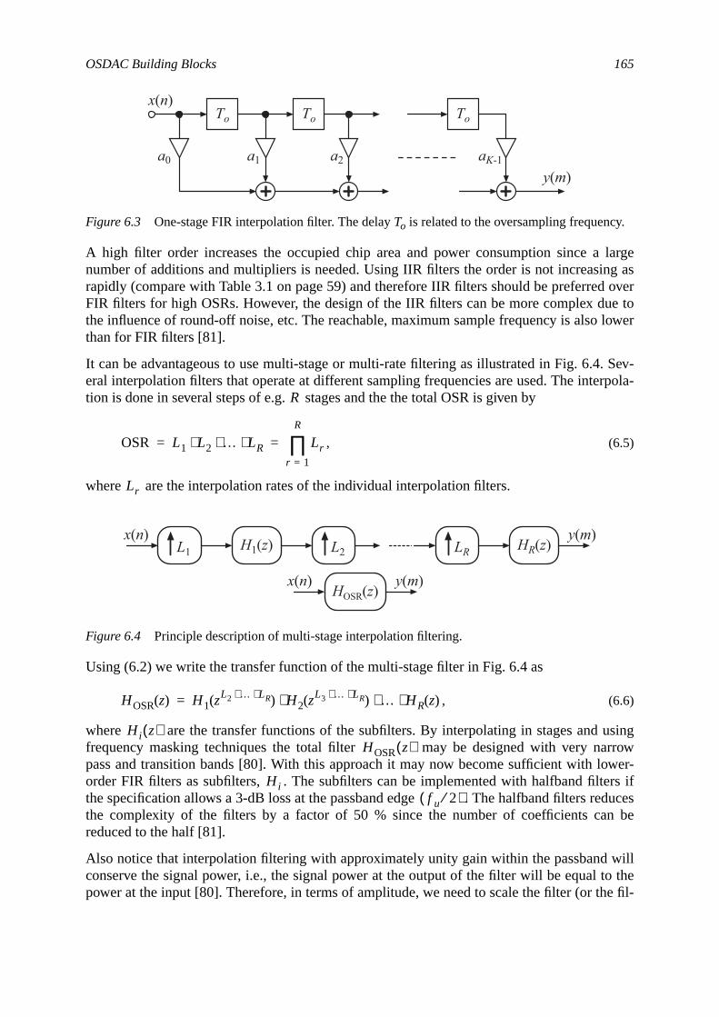
OSDAC Building Blocks 165
largeg asovere tolower
Sev-rpola-
usingrrowwer-rs ifduces
be
willo thee fil-
A high filter order increases the occupied chip area and power consumption since anumber of additions and multipliers is needed. Using IIR filters the order is not increasinrapidly (compare with Table 3.1 on page 59) and therefore IIR filters should be preferredFIR filters for high OSRs. However, the design of the IIR filters can be more complex duthe influence of round-off noise, etc. The reachable, maximum sample frequency is alsothan for FIR filters [81].
It can be advantageous to use multi-stage or multi-rate filtering as illustrated in Fig. 6.4.eral interpolation filters that operate at different sampling frequencies are used. The intetion is done in several steps of e.g. stages and the the total OSR is given by
, (6.5)
where are the interpolation rates of the individual interpolation filters.
Using (6.2) we write the transfer function of the multi-stage filter in Fig. 6.4 as
, (6.6)
where are the transfer functions of the subfilters. By interpolating in stages andfrequency masking techniques the total filter may be designed with very napass and transition bands [80]. With this approach it may now become sufficient with loorder FIR filters as subfilters, . The subfilters can be implemented with halfband filtethe specification allows a 3-dB loss at the passband edge . The halfband filters rethe complexity of the filters by a factor of 50 % since the number of coefficients canreduced to the half [81].
Also notice that interpolation filtering with approximately unity gain within the passbandconserve the signal power, i.e., the signal power at the output of the filter will be equal tpower at the input [80]. Therefore, in terms of amplitude, we need to scale the filter (or th
Figure 6.3 One-stage FIR interpolation filter. The delayTo is related to the oversampling frequency.
Figure 6.4 Principle description of multi-stage interpolation filtering.
a1 a2 aK-1
y(m)
To To To
x(n)
a0
R
OSR L1 L2 … LR⋅ ⋅ ⋅ Lrr 1=
R
∏= =
Lr
L1 H1(z) L2 LR HR(z)x(n) y(m)
x(n) y(m)HOSR(z)
HOSR z( ) H1 zL2 … LR⋅ ⋅( ) H2 zL3 … LR⋅ ⋅( ) … HR z( )⋅ ⋅ ⋅=
Hi z( )HOSR z( )
Hif u 2⁄( )
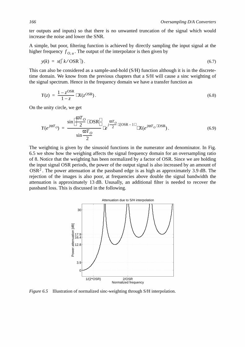
166 Oversampling D/A Converters
ould
the
crete-g of
Fig.ratioldingunt of. The
th ther the
ter outputs and inputs) so that there is no unwanted truncation of the signal which wincrease the noise and lower the SNR.
A simple, but poor, filtering function is achieved by directly sampling the input signal athigher frequency . The output of the interpolator is then given by
. (6.7)
This can also be considered as a sample-and-hold (S/H) function although it is in the distime domain. We know from the previous chapters that a S/H will cause a sinc weightinthe signal spectrum. Hence in the frequency domain we have a transfer function as
. (6.8)
On the unity circle, we get
. (6.9)
The weighting is given by the sinusoid functions in the numerator and denominator. In6.5 we show how the weighing affects the signal frequency domain for an oversamplingof 8. Notice that the weighting has been normalized by a factor of OSR. Since we are hothe input signal OSR periods, the power of the output signal is also increased by an amo
. The power attenuation at the passband edge is as high as approximately 3.9 dBrejection of the images is also poor, at frequencies above double the signal bandwidattenuation is approximately 13 dB. Ususally, an additional filter is needed to recovepassband loss. This is discussed in the following.
Figure 6.5 Illustration of normalized sinc-weighting through S/H interpolation.
f O u,
y k( ) x k OSR⁄( )=
Y z( )1 zOSR–
1 z–-------------------- X zOSR( )⋅=
Y ejωTO( )
ωTO
2----------- OSR⋅
sin
ωTO
2-----------sin
----------------------------------------- ejωTO
2----------- OSR 1–( )⋅
X ejωTO OSR⋅( )⋅ ⋅=
OSR2
1/(2*OSR) 2/OSR
0
3.9
12.8
16.417.9
30
Attenuation due to S/H interpolation
Pow
er a
ttenu
atio
n [d
B]
Normalized frequency
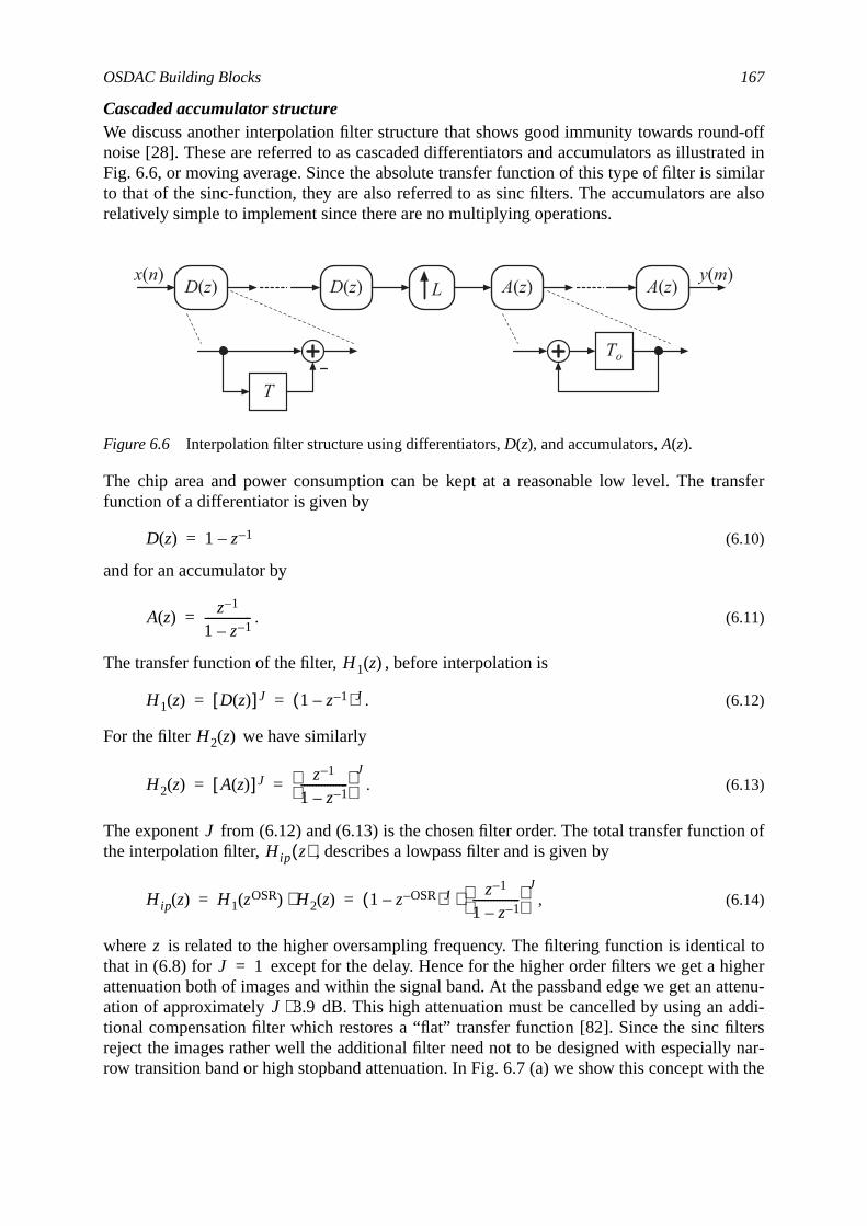
OSDAC Building Blocks 167
d-offated in
ilare also
ansfer
on of
al togherattenu-ddi-
tersnar-
h the
Cascaded accumulator structureWe discuss another interpolation filter structure that shows good immunity towards rounnoise [28]. These are referred to as cascaded differentiators and accumulators as illustrFig. 6.6, or moving average. Since the absolute transfer function of this type of filter is simto that of the sinc-function, they are also referred to as sinc filters. The accumulators arrelatively simple to implement since there are no multiplying operations.
The chip area and power consumption can be kept at a reasonable low level. The trfunction of a differentiator is given by
(6.10)
and for an accumulator by
. (6.11)
The transfer function of the filter, , before interpolation is
. (6.12)
For the filter we have similarly
. (6.13)
The exponent from (6.12) and (6.13) is the chosen filter order. The total transfer functithe interpolation filter, , describes a lowpass filter and is given by
, (6.14)
where is related to the higher oversampling frequency. The filtering function is identicthat in (6.8) for except for the delay. Hence for the higher order filters we get a hiattenuation both of images and within the signal band. At the passband edge we get anation of approximately dB. This high attenuation must be cancelled by using an ational compensation filter which restores a “flat” transfer function [82]. Since the sinc filreject the images rather well the additional filter need not to be designed with especiallyrow transition band or high stopband attenuation. In Fig. 6.7 (a) we show this concept wit
Figure 6.6 Interpolation filter structure using differentiators,D(z), and accumulators,A(z).
x(n) y(m)LD(z) A(z)D(z) A(z)
To
T
D z( ) 1 z 1––=
A z( ) z 1–
1 z 1––----------------=
H1 z( )
H1 z( ) D z( )[ ]J 1 z 1––( )J= =
H2 z( )
H2 z( ) A z( )[ ]J z 1–
1 z 1––----------------
J= =
JHip z( )
Hip z( ) H1 zOSR( ) H2 z( )⋅ 1 z OSR––( )J z 1–
1 z 1––----------------
J⋅= =
zJ 1=
J 3.9⋅
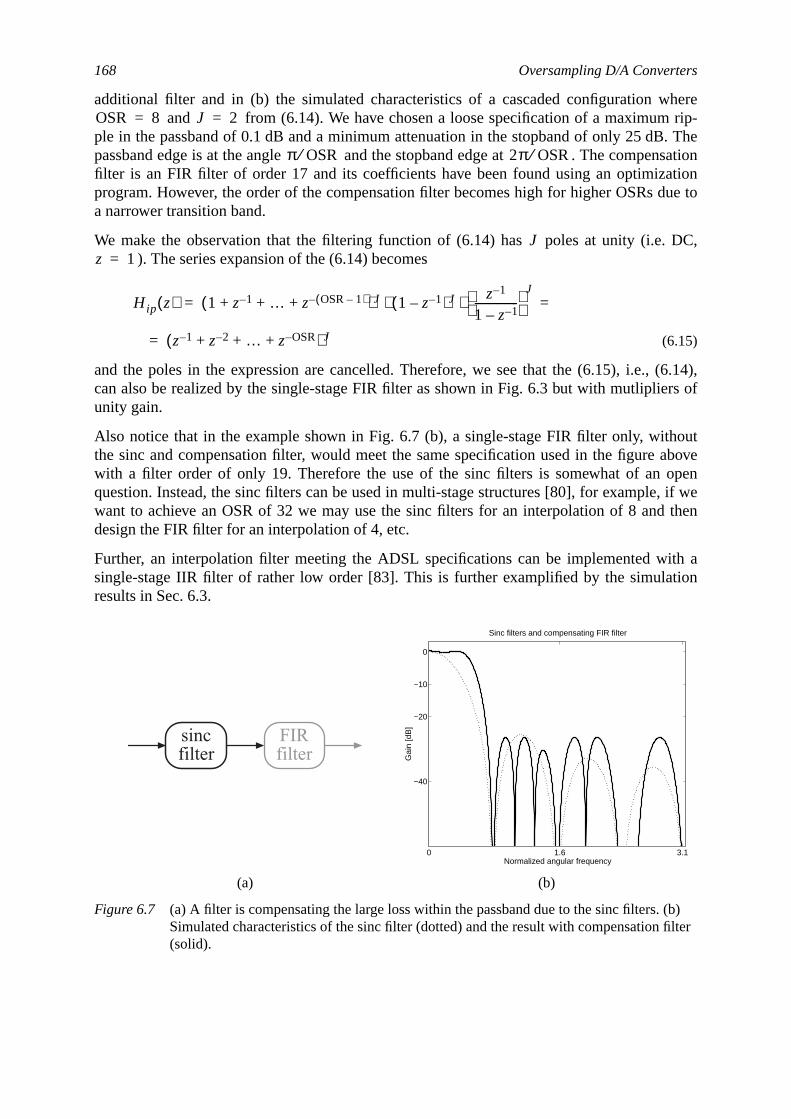
168 Oversampling D/A Converters
hererip-. Thesationtionue to
DC,
(6.14),rs of
outabovepen
, if wethen
ith aion
(b)filter
additional filter and in (b) the simulated characteristics of a cascaded configuration wand from (6.14). We have chosen a loose specification of a maximum
ple in the passband of 0.1 dB and a minimum attenuation in the stopband of only 25 dBpassband edge is at the angle and the stopband edge at . The compenfilter is an FIR filter of order 17 and its coefficients have been found using an optimizaprogram. However, the order of the compensation filter becomes high for higher OSRs da narrower transition band.
We make the observation that the filtering function of (6.14) has poles at unity (i.e.). The series expansion of the (6.14) becomes
(6.15)
and the poles in the expression are cancelled. Therefore, we see that the (6.15), i.e.,can also be realized by the single-stage FIR filter as shown in Fig. 6.3 but with mutliplieunity gain.
Also notice that in the example shown in Fig. 6.7 (b), a single-stage FIR filter only, withthe sinc and compensation filter, would meet the same specification used in the figurewith a filter order of only 19. Therefore the use of the sinc filters is somewhat of an oquestion. Instead, the sinc filters can be used in multi-stage structures [80], for examplewant to achieve an OSR of 32 we may use the sinc filters for an interpolation of 8 anddesign the FIR filter for an interpolation of 4, etc.
Further, an interpolation filter meeting the ADSL specifications can be implemented wsingle-stage IIR filter of rather low order [83]. This is further examplified by the simulatresults in Sec. 6.3.
(a) (b)
Figure 6.7 (a) A filter is compensating the large loss within the passband due to the sinc filters.Simulated characteristics of the sinc filter (dotted) and the result with compensation (solid).
OSR 8= J 2=
π OSR⁄ 2π OSR⁄
Jz 1=
Hip z( ) 1 z 1– … z OSR 1–( )–+ + +( )J 1 z 1––( )J z 1–
1 z 1––----------------
J⋅ ⋅= =
z 1– z 2– … z OSR–+ + +( ) J=
sincfilter
FIRfilter
0 1.6 3.1
−40
−20
−10
0
Sinc filters and compensating FIR filter
Normalized angular frequency
Gai
n [d
B]
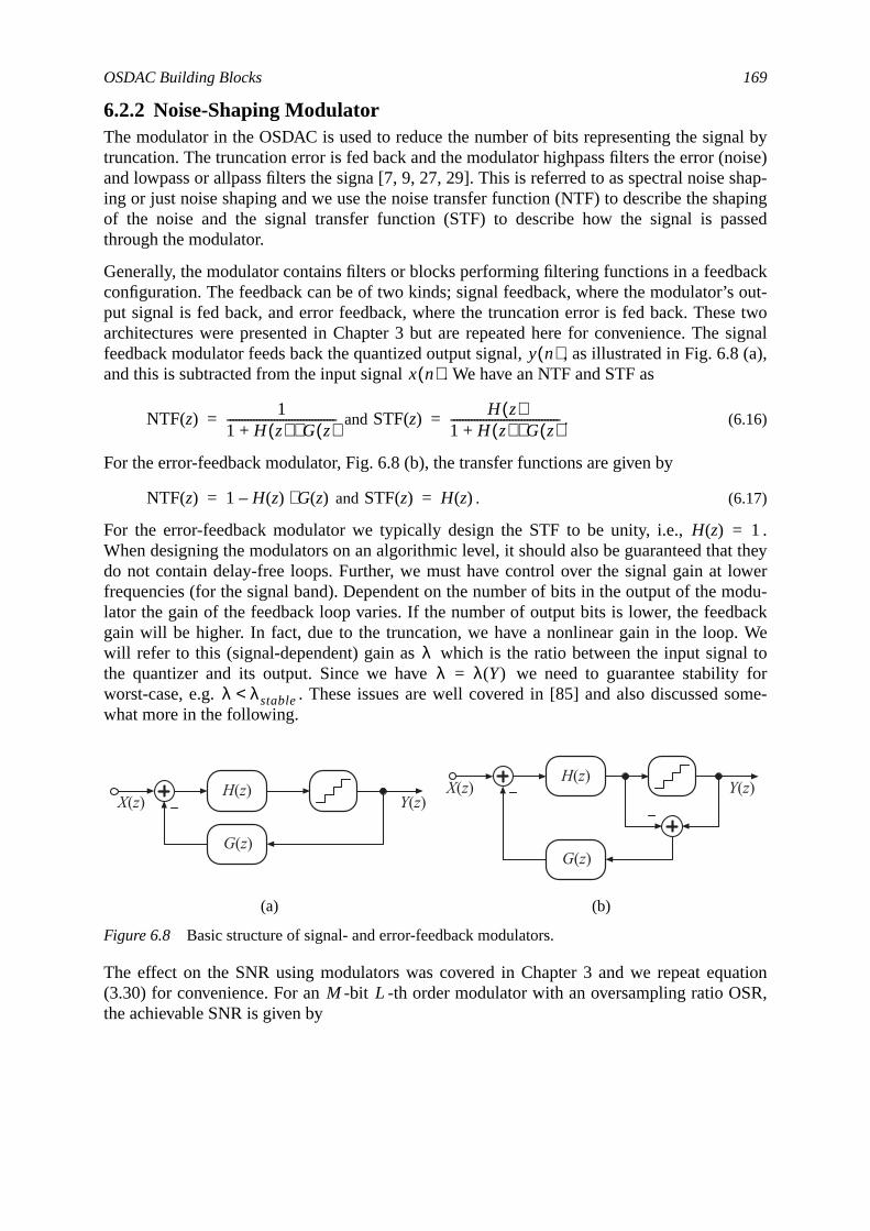
OSDAC Building Blocks 169
al byoise)shap-apingssed
acks out-e twosignal
.8 (a),
.t theylowerodu-
back. Weal toy forsome-
uationSR,
6.2.2 Noise-Shaping ModulatorThe modulator in the OSDAC is used to reduce the number of bits representing the signtruncation. The truncation error is fed back and the modulator highpass filters the error (nand lowpass or allpass filters the signa [7, 9, 27, 29]. This is referred to as spectral noiseing or just noise shaping and we use the noise transfer function (NTF) to describe the shof the noise and the signal transfer function (STF) to describe how the signal is pathrough the modulator.
Generally, the modulator contains filters or blocks performing filtering functions in a feedbconfiguration. The feedback can be of two kinds; signal feedback, where the modulator’put signal is fed back, and error feedback, where the truncation error is fed back. Thesarchitectures were presented in Chapter 3 but are repeated here for convenience. Thefeedback modulator feeds back the quantized output signal, , as illustrated in Fig. 6and this is subtracted from the input signal . We have an NTF and STF as
and . (6.16)
For the error-feedback modulator, Fig. 6.8 (b), the transfer functions are given by
and . (6.17)
For the error-feedback modulator we typically design the STF to be unity, i.e.,When designing the modulators on an algorithmic level, it should also be guaranteed thado not contain delay-free loops. Further, we must have control over the signal gain atfrequencies (for the signal band). Dependent on the number of bits in the output of the mlator the gain of the feedback loop varies. If the number of output bits is lower, the feedgain will be higher. In fact, due to the truncation, we have a nonlinear gain in the loopwill refer to this (signal-dependent) gain as which is the ratio between the input signthe quantizer and its output. Since we have we need to guarantee stabilitworst-case, e.g. . These issues are well covered in [85] and also discussedwhat more in the following.
The effect on the SNR using modulators was covered in Chapter 3 and we repeat eq(3.30) for convenience. For an -bit -th order modulator with an oversampling ratio Othe achievable SNR is given by
(a) (b)
Figure 6.8 Basic structure of signal- and error-feedback modulators.
y n( )x n( )
NTF z( ) 11 H z( ) G z( )⋅+-------------------------------------= STF z( ) H z( )
1 H z( ) G z( )⋅+-------------------------------------=
NTF z( ) 1 H z( ) G z( )⋅–= STF z( ) H z( )=
H z( ) 1=
λλ λ Y( )=
λ λstable<
H(z)
G(z)
Y(z)X(z)
H(z)
G(z)
Y(z)X(z)
M L
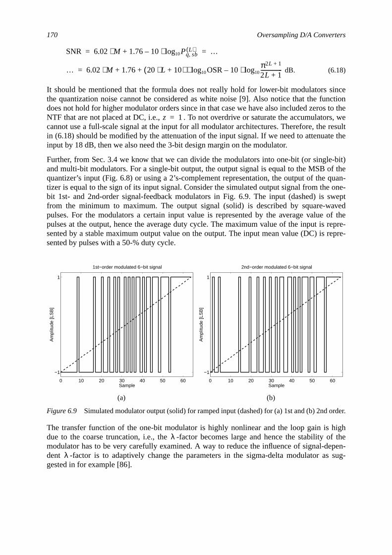
170 Oversampling D/A Converters
incectionto the
s, weresultte the
-bit)f thequan-one-weptvedof therepre-repre-
highof thepen-
s sug-
rder.
dB. (6.18)
It should be mentioned that the formula does not really hold for lower-bit modulators sthe quantization noise cannot be considered as white noise [9]. Also notice that the fundoes not hold for higher modulator orders since in that case we have also included zerosNTF that are not placed at DC, i.e., . To not overdrive or saturate the accumulatorcannot use a full-scale signal at the input for all modulator architectures. Therefore, thein (6.18) should be modified by the attenuation of the input signal. If we need to attenuainput by 18 dB, then we also need the 3-bit design margin on the modulator.
Further, from Sec. 3.4 we know that we can divide the modulators into one-bit (or singleand multi-bit modulators. For a single-bit output, the output signal is equal to the MSB oquantizer’s input (Fig. 6.8) or using a 2’s-complement representation, the output of thetizer is equal to the sign of its input signal. Consider the simulated output signal from thebit 1st- and 2nd-order signal-feedback modulators in Fig. 6.9. The input (dashed) is sfrom the minimum to maximum. The output signal (solid) is described by square-wapulses. For the modulators a certain input value is represented by the average valuepulses at the output, hence the average duty cycle. The maximum value of the input issented by a stable maximum output value on the output. The input mean value (DC) issented by pulses with a 50-% duty cycle.
The transfer function of the one-bit modulator is highly nonlinear and the loop gain isdue to the coarse truncation, i.e., the -factor becomes large and hence the stabilitymodulator has to be very carefully examined. A way to reduce the influence of signal-dedent -factor is to adaptively change the parameters in the sigma-delta modulator agested in for example [86].
(a) (b)
Figure 6.9 Simulated modulator output (solid) for ramped input (dashed) for (a) 1st and (b) 2nd o
SNR 6.02 M⋅ 1.76 10 Pq sb,L( )log10⋅–+ …= =
… 6.02 M⋅ 1.76 20 L⋅ 10+( ) OSRlog10⋅ 10π2L 1+
2L 1+----------------log10⋅–+ +=
z 1=
0 10 20 30 40 50 60
−1
1
Sample
Am
plitu
de [L
SB
]
1st−order modulated 6−bit signal
0 10 20 30 40 50 60
−1
1
Sample
Am
plitu
de [L
SB
]
2nd−order modulated 6−bit signal
λ
λ
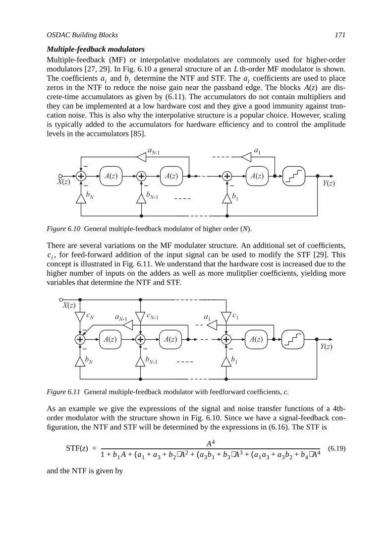
OSDAC Building Blocks 171
rderown.placere dis-s andt trun-aling
itude
ients,histo theore
a 4th-con-
Multiple-feedback modulatorsMultiple-feedback (MF) or interpolative modulators are commonly used for higher-omodulators [27, 29]. In Fig. 6.10 a general structure of an th-order MF modulator is shThe coefficients and determine the NTF and STF. The coefficients are used tozeros in the NTF to reduce the noise gain near the passband edge. The blocks acrete-time accumulators as given by (6.11). The accumulators do not contain multiplierthey can be implemented at a low hardware cost and they give a good immunity againscation noise. This is also why the interpolative structure is a popular choice. However, scis typically added to the accumulators for hardware efficiency and to control the ampllevels in the accumulators [85].
There are several variations on the MF modulater structure. An additional set of coeffic, for feed-forward addition of the input signal can be used to modify the STF [29]. T
concept is illustrated in Fig. 6.11. We understand that the hardware cost is increased duehigher number of inputs on the adders as well as more mulitplier coefficients, yielding mvariables that determine the NTF and STF.
As an example we give the expressions of the signal and noise transfer functions oforder modulator with the structure shown in Fig. 6.10. Since we have a signal-feedbackfiguration, the NTF and STF will be determined by the expressions in (6.16). The STF is
(6.19)
and the NTF is given by
Figure 6.10 General multiple-feedback modulator of higher order (N).
Figure 6.11 General multiple-feedback modulator with feedforward coefficients,c.
Lai bi ai
A z( )
b1bN-1bN
aN-1 a1
Y(z)X(z)A(z) A(z) A(z)
ci
A(z) A(z) A(z)
b1bN-1bN
aN-1 a1
Y(z)
X(z)c1cN-1cN
STF z( ) A4
1 b1A a1 a3 b2+ +( )A2 a3b1 b3+( )A3 a1a3 a3b2 b4+ +( )A4+ + + +----------------------------------------------------------------------------------------------------------------------------------------------------------------------=
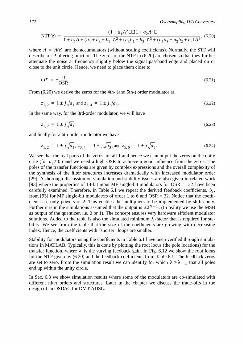
172 Oversampling D/A Converters
willrtheron or
e unityTheity oforderworkeens, ,ffi-
only.SB
ulatorsta-sing
ula-heocuszerosles
withn the
, (6.20)
where are the accumulators (without scaling coefficients). Normally, the STFdescribe a LP filtering function. The zeros of the NTF in (6.20) are chosen so that they fuattenuate the noise at frequency slightly below the signal passband edge and placedclose to the unit circle. Hence, we need to place them close to
. (6.21)
From (6.20) we derive the zeros for the 4th- (and 5th-) order modulator as
and . (6.22)
In the same way, for the 3rd-order modulator, we will have
(6.23)
and finally for a 6th-order modulator we have
, , and . (6.24)
We see that the real parts of the zeros are all 1 and hence we cannot put the zeros on thcirle (for ) and we need a high OSR to achieve a good influence from the zeros.poles of the transfer functions are given by complex expressions and the overall complexthe synthesis of the filter structures increases dramatically with increased modulator[29]. A thorough discussion on simulation and stability issues are also given in related[93] where the properties of 14-bit input MF single-bit modulators for have bcarefully examined. Therefore, in Table 6.1 we repeat the derived feedback coefficientfrom [93] for MF single-bit modulators of order 1 to 6 and OSR = 32. Notice that the coecients are only powers of 2. This enables the multipliers to be implemented by shiftsFurther it is in the simulations assumed that the output is . (In reality we use the Mas output of the quantizer, i.e. 0 or 1). The concept ensures very hardware efficient modsolutions. Added to the table is also the simulated minimum -factor that is required forbility. We see from the table that the size of the coefficients are growing with decreaindex. Hence, the coefficients with “shorter” loops are smaller.
Stability for modulators using the coefficients in Table 6.1 have been verified through simtions in MATLAB. Typically, this is done by plotting the root locus (the pole locations) for ttransfer function, where is the varying feedback gain. In Fig. 6.12 we show the root lfor the NTF given by (6.20) and the feedback coefficients from Table 6.1. The feedbackare set to zero. From the simulation result we can identify for which that all poend up within the unity circle.
In Sec. 6.3 we show simulation results where some of the modulators are co-simulateddifferent filter orders and structures. Later in the chapter we discuss the trade-offs idesign of an OSDAC for DMT-ADSL.
NTF z( )1 a1A2+( ) 1 a2A2+( )⋅
1 b1A a1 a3 b2+ +( )A2 a3b1 b3+( )A3 a1a3 a3b2 b4+ +( )A4+ + + +----------------------------------------------------------------------------------------------------------------------------------------------------------------------=
A A z( )=
ωTπ
OSR-----------±=
z1 2, 1 j a1±= z3 4, 1 j a3±=
z1 2, 1 j a1±=
z1 2, 1 j a1±= z3 4, 1 j a3±= z5 6, 1 j a5±=
ai 0≠
OSR 32=bi
2N 1–±
λ
λ
λ λmin>
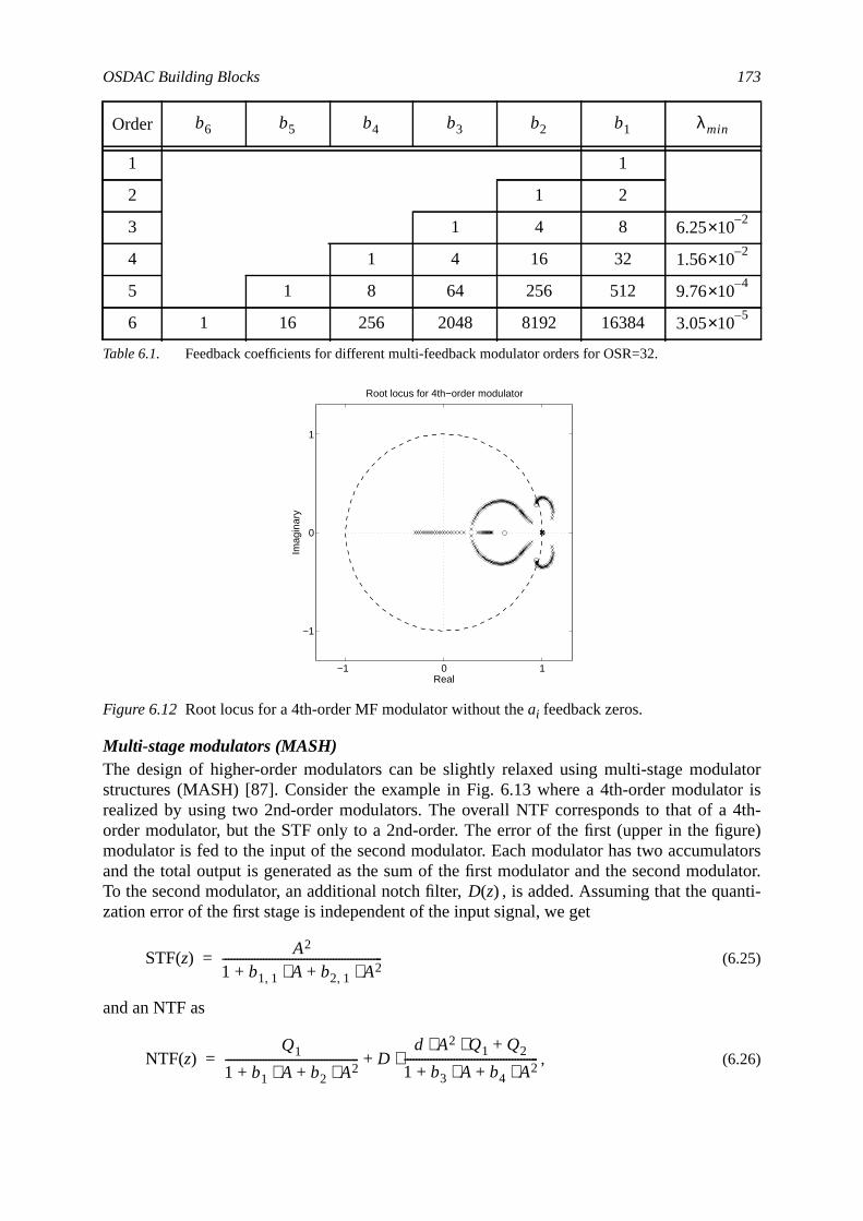
OSDAC Building Blocks 173
latoror is4th-ure)latorsulator.anti-
Multi-stage modulators (MASH)The design of higher-order modulators can be slightly relaxed using multi-stage modustructures (MASH) [87]. Consider the example in Fig. 6.13 where a 4th-order modulatrealized by using two 2nd-order modulators. The overall NTF corresponds to that of aorder modulator, but the STF only to a 2nd-order. The error of the first (upper in the figmodulator is fed to the input of the second modulator. Each modulator has two accumuand the total output is generated as the sum of the first modulator and the second modTo the second modulator, an additional notch filter, , is added. Assuming that the quzation error of the first stage is independent of the input signal, we get
(6.25)
and an NTF as
, (6.26)
Order
1 1
2 1 2
3 1 4 8
4 1 4 16 32
5 1 8 64 256 512
6 1 16 256 2048 8192 16384
Table 6.1. Feedback coefficients for different multi-feedback modulator orders for OSR=32.
Figure 6.12 Root locus for a 4th-order MF modulator without theai feedback zeros.
b6 b5 b4 b3 b2 b1 λmin
6.252–×10
1.562–×10
9.764–×10
3.055–×10
−1 0 1
−1
0
1
Real
Imag
inar
y
Root locus for 4th−order modulator
D z( )
STF z( ) A2
1 b1 1, A⋅ b2 1, A2⋅+ +-------------------------------------------------------=
NTF z( )Q1
1 b1 A⋅ b2 A2⋅+ +---------------------------------------------- D
d A2 Q1⋅ ⋅ Q2+
1 b3 A⋅ b4 A2⋅+ +----------------------------------------------⋅+=
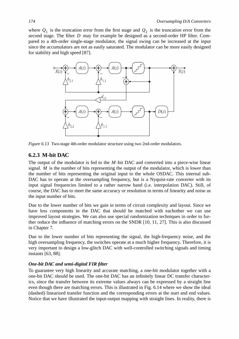
174 Oversampling D/A Converters
theCom-input
esigned
nearthansub-th its, ofise as
wen useto fur-ussed
d thee, it ising
ith acter-ht lineideal
values.re is
where is the truncation error from the first stage and is the truncation error fromsecond stage. The filter may for example be designed as a second-order HP filter.pared to a 4th-order single-stage modulator, the signal swing can be increased at thesince the accumulators are not as easily saturated. The modulator can be more easily dfor stability and high speed [87].
6.2.3 M-bit DACThe output of the modulator is fed to the -bit DAC and converted into a piece-wise lisignal. is the number of bits representing the output of the modulator, which is lowerthe number of bits representing the original input to the whole OSDAC. This internalDAC has to operate at the oversampling frequency, but is a Nyquist-rate converter wiinput signal frequencies limited to a rather narrow band (i.e. interpolation DAC). Stillcourse, the DAC has to meet the same accuracy or resolution in terms of linearity and nothe input number of bits.
Due to the lower number of bits we gain in terms of circuit complexity and layout. Sincehave less components in the DAC that should be matched with eachother we caimproved layout strategies. We can also use special randomization techniques in orderther reduce the influence of matching errors on the SNDR [10, 11, 27]. This is also discin Chapter 7.
Due to the lower number of bits representing the signal, the high-frequency noise, anhigh oversampling frequency, the switches operate at a much higher frequency. Thereforvery important to design a low-glitch DAC with well-controlled switching signals and timinstants [63, 88].
One-bit DAC and semi-digital FIR filterTo guarantee very high linearity and accurate matching, a one-bit modulator together wone-bit DAC should be used. The one-bit DAC has an infinitely linear DC transfer charaics, since the transfer between its extreme values always can be expressed by a straigeven though there are matching errors. This is illustrated in Fig. 6.14 where we show the(dashed) linearized transfer function and the corresponding errors at the start and endNotice that we have illustrated the input-output mapping with straight lines. In reality, the
Figure 6.13 Two-stage 4th-order modulator structure using two 2nd-order modulators.
Q1 Q2D
b1,1
b1,2
b2,1
d12
b2,2
Y(z)X(z)
A(z) A(z)
A(z) A(z)
D(z)
MM
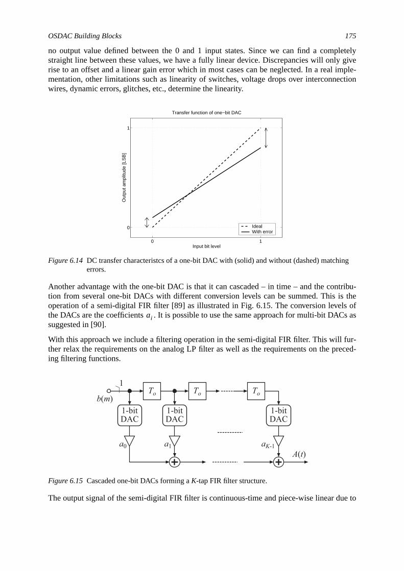
OSDAC Building Blocks 175
letelygive
imple-ction
tribu-the
s ofs as
ur-reced-
e to
ng
no output value defined between the 0 and 1 input states. Since we can find a compstraight line between these values, we have a fully linear device. Discrepancies will onlyrise to an offset and a linear gain error which in most cases can be neglected. In a realmentation, other limitations such as linearity of switches, voltage drops over interconnewires, dynamic errors, glitches, etc., determine the linearity.
Another advantage with the one-bit DAC is that it can cascaded – in time – and the contion from several one-bit DACs with different conversion levels can be summed. This isoperation of a semi-digital FIR filter [89] as illustrated in Fig. 6.15. The conversion levelthe DACs are the coefficients . It is possible to use the same approach for multi-bit DACsuggested in [90].
With this approach we include a filtering operation in the semi-digital FIR filter. This will fther relax the requirements on the analog LP filter as well as the requirements on the ping filtering functions.
The output signal of the semi-digital FIR filter is continuous-time and piece-wise linear du
Figure 6.14 DC transfer characteristcs of a one-bit DAC with (solid) and without (dashed) matchierrors.
Figure 6.15 Cascaded one-bit DACs forming aK-tap FIR filter structure.
0 1
0
1
Input bit level
Out
put a
mpl
itude
[LS
B]
Transfer function of one−bit DAC
Ideal With error
ai
b(m)To
1-bitDAC
1-bitDAC
1-bitDAC
To To
1
a1 aK-1a0A(t)
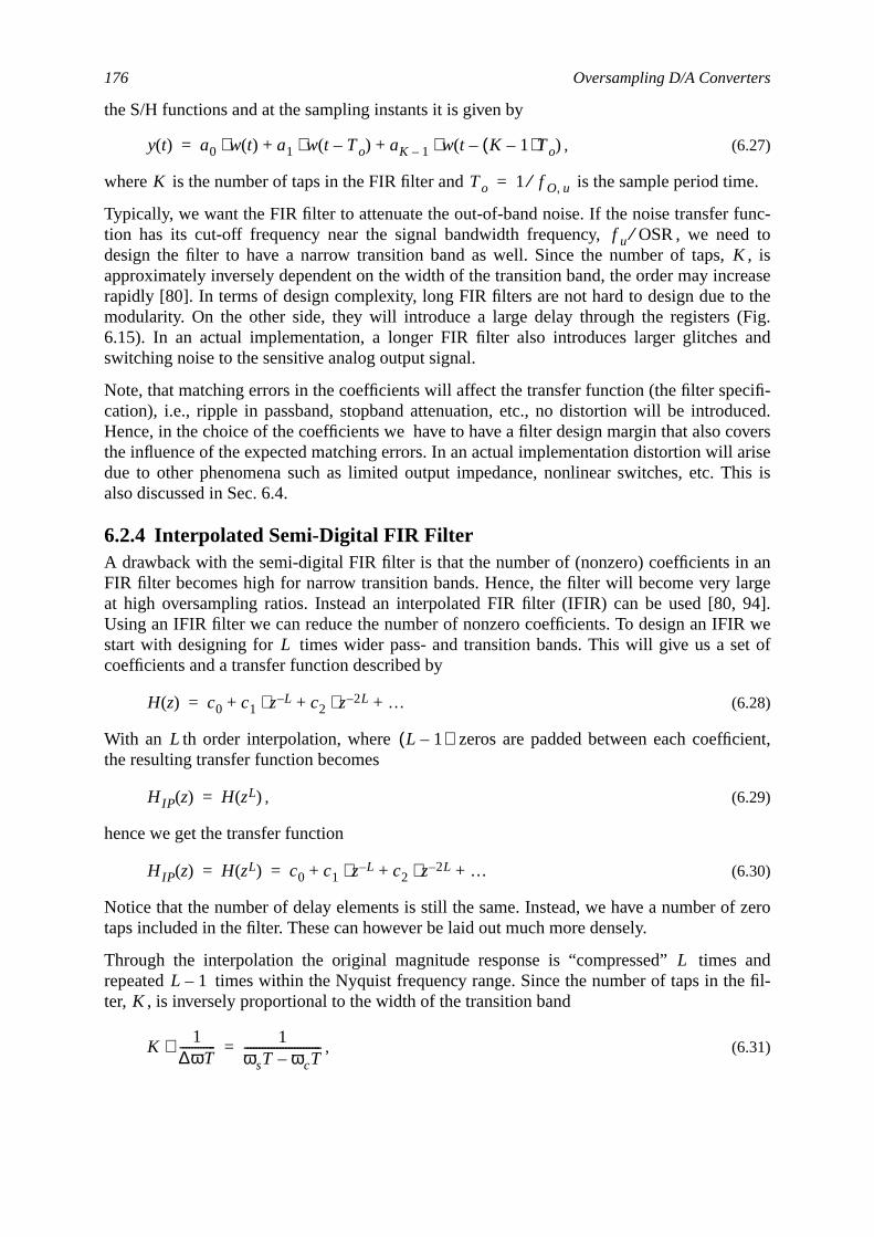
176 Oversampling D/A Converters
e.
unc-d to
, isreasethe
(Fig.and
cifi-uced.oversarisehis is
anarge94].
R weet of
cient,
f zero
ande fil-
the S/H functions and at the sampling instants it is given by
, (6.27)
where is the number of taps in the FIR filter and is the sample period tim
Typically, we want the FIR filter to attenuate the out-of-band noise. If the noise transfer ftion has its cut-off frequency near the signal bandwidth frequency, , we needesign the filter to have a narrow transition band as well. Since the number of taps,approximately inversely dependent on the width of the transition band, the order may incrapidly [80]. In terms of design complexity, long FIR filters are not hard to design due tomodularity. On the other side, they will introduce a large delay through the registers6.15). In an actual implementation, a longer FIR filter also introduces larger glitchesswitching noise to the sensitive analog output signal.
Note, that matching errors in the coefficients will affect the transfer function (the filter specation), i.e., ripple in passband, stopband attenuation, etc., no distortion will be introdHence, in the choice of the coefficients we have to have a filter design margin that also cthe influence of the expected matching errors. In an actual implementation distortion willdue to other phenomena such as limited output impedance, nonlinear switches, etc. Talso discussed in Sec. 6.4.
6.2.4 Interpolated Semi-Digital FIR FilterA drawback with the semi-digital FIR filter is that the number of (nonzero) coefficients inFIR filter becomes high for narrow transition bands. Hence, the filter will become very lat high oversampling ratios. Instead an interpolated FIR filter (IFIR) can be used [80,Using an IFIR filter we can reduce the number of nonzero coefficients. To design an IFIstart with designing for times wider pass- and transition bands. This will give us a scoefficients and a transfer function described by
(6.28)
With an th order interpolation, where zeros are padded between each coeffithe resulting transfer function becomes
, (6.29)
hence we get the transfer function
(6.30)
Notice that the number of delay elements is still the same. Instead, we have a number otaps included in the filter. These can however be laid out much more densely.
Through the interpolation the original magnitude response is “compressed” timesrepeated times within the Nyquist frequency range. Since the number of taps in thter, , is inversely proportional to the width of the transition band
, (6.31)
y t( ) a0 w t( )⋅ a1 w t To–( )⋅ aK 1– w t K 1–( )To–( )⋅+ +=
K To 1 f O u,⁄=
f u OSR⁄K
L
H z( ) c0 c1 z L–⋅ c2 z 2L–⋅ …+ + +=
L L 1–( )
HIP z( ) H zL( )=
HIP z( ) H zL( ) c0 c1 z L–⋅ c2 z 2L–⋅ …+ + += =
LL 1–
K
K1
∆ωT------------∼ 1
ωsT ωcT–--------------------------=
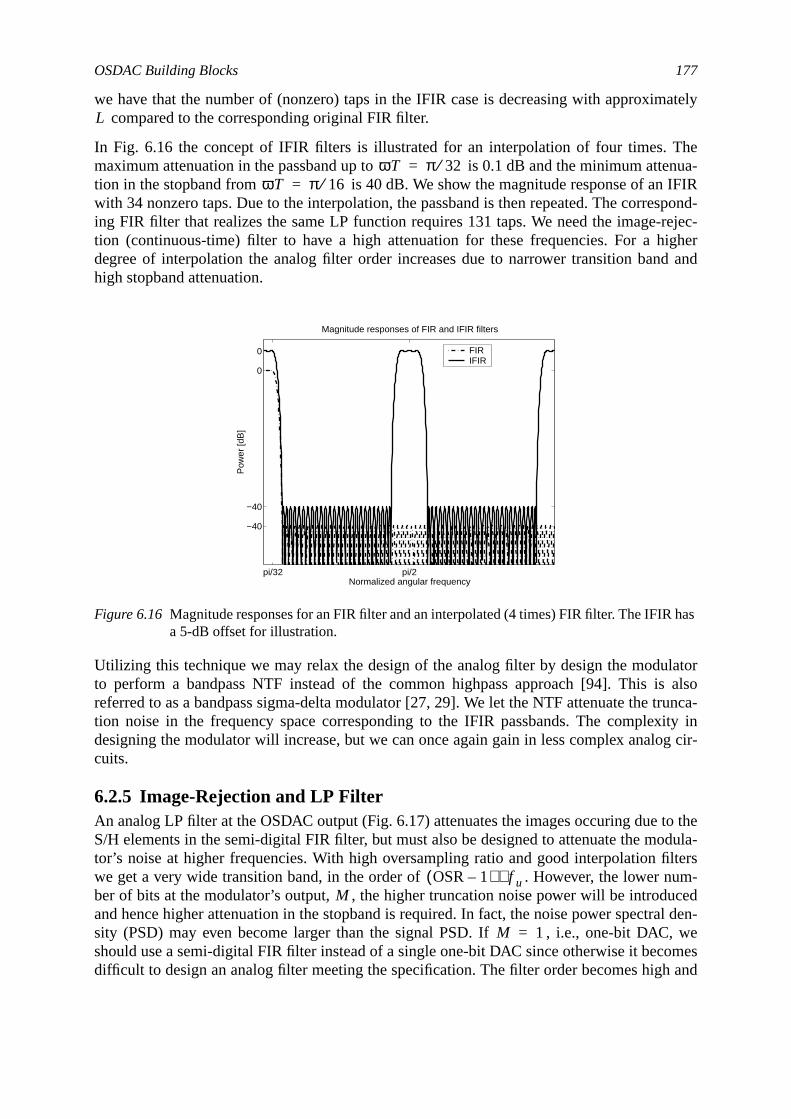
OSDAC Building Blocks 177
ately
henua-IFIRspond-rejec-igherd and
latoralso
runca-ity ing cir-
to thedula-ltersm-ced
al den-, wemesand
has
we have that the number of (nonzero) taps in the IFIR case is decreasing with approxim compared to the corresponding original FIR filter.
In Fig. 6.16 the concept of IFIR filters is illustrated for an interpolation of four times. Tmaximum attenuation in the passband up to is 0.1 dB and the minimum attetion in the stopband from is 40 dB. We show the magnitude response of anwith 34 nonzero taps. Due to the interpolation, the passband is then repeated. The correing FIR filter that realizes the same LP function requires 131 taps. We need the image-tion (continuous-time) filter to have a high attenuation for these frequencies. For a hdegree of interpolation the analog filter order increases due to narrower transition banhigh stopband attenuation.
Utilizing this technique we may relax the design of the analog filter by design the moduto perform a bandpass NTF instead of the common highpass approach [94]. This isreferred to as a bandpass sigma-delta modulator [27, 29]. We let the NTF attenuate the ttion noise in the frequency space corresponding to the IFIR passbands. The complexdesigning the modulator will increase, but we can once again gain in less complex analocuits.
6.2.5 Image-Rejection and LP FilterAn analog LP filter at the OSDAC output (Fig. 6.17) attenuates the images occuring dueS/H elements in the semi-digital FIR filter, but must also be designed to attenuate the motor’s noise at higher frequencies. With high oversampling ratio and good interpolation fiwe get a very wide transition band, in the order of . However, the lower nuber of bits at the modulator’s output, , the higher truncation noise power will be introduand hence higher attenuation in the stopband is required. In fact, the noise power spectrsity (PSD) may even become larger than the signal PSD. If , i.e., one-bit DACshould use a semi-digital FIR filter instead of a single one-bit DAC since otherwise it becodifficult to design an analog filter meeting the specification. The filter order becomes high
Figure 6.16 Magnitude responses for an FIR filter and an interpolated (4 times) FIR filter. The IFIRa 5-dB offset for illustration.
L
ωT π 32⁄=ωT π 16⁄=
pi/32 pi/2
−40
−40
0
0
Normalized angular frequency
Pow
er [d
B]
Magnitude responses of FIR and IFIR filters
FIR IFIR
OSR 1–( ) f u⋅M
M 1=
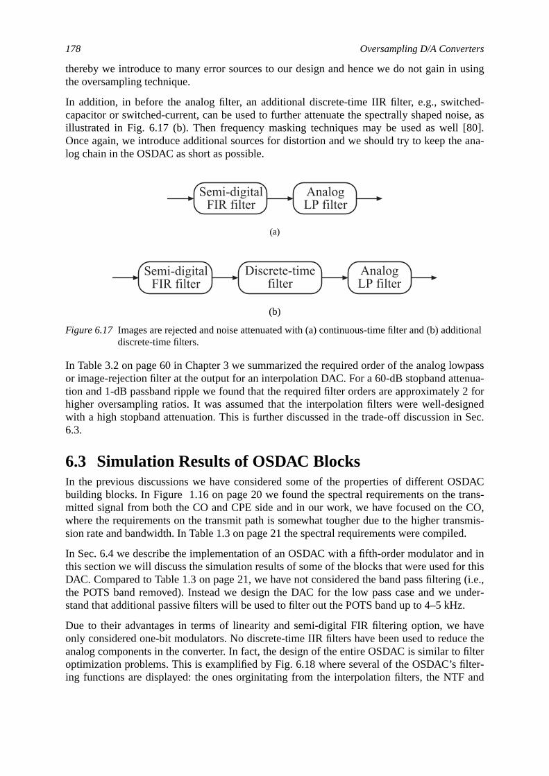
178 Oversampling D/A Converters
using
ed-ise, as[80].ana-
wpassnua-2 for
ignedSec.
DACtrans-
CO,nsmis-led.
d inr thisg (i.e.,under-z.
avece thefilterlter-and
itional
thereby we introduce to many error sources to our design and hence we do not gain inthe oversampling technique.
In addition, in before the analog filter, an additional discrete-time IIR filter, e.g., switchcapacitor or switched-current, can be used to further attenuate the spectrally shaped noillustrated in Fig. 6.17 (b). Then frequency masking techniques may be used as wellOnce again, we introduce additional sources for distortion and we should try to keep thelog chain in the OSDAC as short as possible.
In Table 3.2 on page 60 in Chapter 3 we summarized the required order of the analog loor image-rejection filter at the output for an interpolation DAC. For a 60-dB stopband attetion and 1-dB passband ripple we found that the required filter orders are approximatelyhigher oversampling ratios. It was assumed that the interpolation filters were well-deswith a high stopband attenuation. This is further discussed in the trade-off discussion in6.3.
6.3 Simulation Results of OSDAC BlocksIn the previous discussions we have considered some of the properties of different OSbuilding blocks. In Figure 1.16 on page 20 we found the spectral requirements on themitted signal from both the CO and CPE side and in our work, we have focused on thewhere the requirements on the transmit path is somewhat tougher due to the higher trasion rate and bandwidth. In Table 1.3 on page 21 the spectral requirements were compi
In Sec. 6.4 we describe the implementation of an OSDAC with a fifth-order modulator anthis section we will discuss the simulation results of some of the blocks that were used foDAC. Compared to Table 1.3 on page 21, we have not considered the band pass filterinthe POTS band removed). Instead we design the DAC for the low pass case and westand that additional passive filters will be used to filter out the POTS band up to 4–5 kH
Due to their advantages in terms of linearity and semi-digital FIR filtering option, we honly considered one-bit modulators. No discrete-time IIR filters have been used to reduanalog components in the converter. In fact, the design of the entire OSDAC is similar tooptimization problems. This is examplified by Fig. 6.18 where several of the OSDAC’s fiing functions are displayed: the ones orginitating from the interpolation filters, the NTF
(a)
(b)
Figure 6.17 Images are rejected and noise attenuated with (a) continuous-time filter and (b) adddiscrete-time filters.
Semi-digitalFIR filter
AnalogLP filter
Semi-digitalFIR filter
Discrete-timefilter
AnalogLP filter
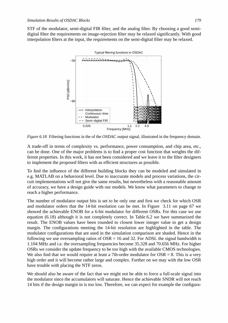
Simulation Results of OSDAC Blocks 179
emi-ood.
etc.,e dif-igners
d ine cir-mountnge to
OSR7 we
e used theesignThein the
th isigher
ogies.very
OSR
l intoreachura-
ain.
STF of the modulator, semi-digital FIR filter, and the analog filter. By choosing a good sdigital filter the requirements on image-rejection filter may be relaxed significantly. With ginterpolation filters at the input, the requirements on the semi-digital filter may be relaxed
A trade-off in terms of complexity vs. performance, power consumption, and chip area,can be done. One of the major problems is to find a proper cost function that weights thferent properties. In this work, it has not been considered and we leave it to the filter desto implement the proposed filters with as efficient structures as possible.
To find the influence of the different building blocks they can be modeled and simulatee.g. MATLAB on a behavioral level. Due to inaccurate models and process variations, thcuit implementations will not give the same results, but nevertheless with a reasonable aof accuracy, we have a design guide with our models. We know what parameters to chareach a higher performance.
The number of modulator output bits is set to be only one and first we check for whichand modulator orders that the 14-bit resolution can be met. In Figure 3.11 on page 6showed the achievable ENOB for a 6-bit modulator for different OSRs. For this case wequation (6.18) although it is not completely correct. In Table 6.2 we have summarizeresult. The ENOB values have been rounded to closest lower integer value to get a dmargin. The configurations meeting the 14-bit resolution are highlighted in the table.modulator configurations that are used in the simulation comparison are shaded. Hencefollowing we use oversampling ratios of OSR = 16 and 32. For ADSL the signal bandwid1.104 MHz and i.e. the oversampling frequencies become 35.328 and 70.656 MHz. For hOSRs we consider the update frequency to be too high with the available CMOS technolWe also find that we would require at least a 7th-order modulator for OSR = 8. This is ahigh order and it will become rather large and complex. Further on we may with the lowhave trouble with placing the NTF zeros.
We should also be aware of the fact that we might not be able to force a full-scale signathe modulator since the accumulators will saturate. Hence the achievable SNDR will not14 bits if the design margin in is too low. Therefore, we can expect for example the config
Figure 6.18 Filtering functions in the of the OSDAC output signal, illustrated in the frequency dom
0.026 1.1 2.2 4.9
−90
−36
Typical filtering functions in OSDAC
PS
D [d
Bm
/Hz]
Frequency [MHz]
Interpolation Continuous−time Modulator Semi−digital FIR
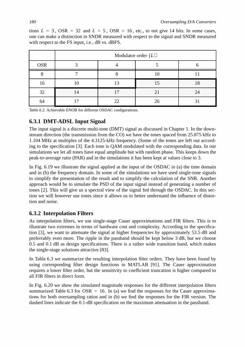
180 Oversampling D/A Converters
es,sured
own-kHz tocord-
ourn the
ainignalstherber ofsec-istor-
is toifica-
andhoose
akes
d byiond to
filtersima-
. Theand.
tions , and , , etc., to not give 14 bits. In some casone can make a distinction in SNDR measured with respect to the signal and SNDR meawith respect to the FS input, i.e., dB vs. dBFS.
6.3.1 DMT-ADSL Input SignalThe input signal is a discrete multi-tone (DMT) signal as discussed in Chapter 1. In the dstream direction (the transmission from the CO) we have the tones spaced from 25.8751.104 MHz at multiples of the 4.3125-kHz frequency. (Some of the tones are left out acing to the specification [3]. Each tone is QAM modulated with the corresponding data. Insimulations we let all tones have equal amplitude but with random phase. This keeps dowpeak-to-average ratio (PAR) and in the simulations it has been kept at values close to 3.
In Fig. 6.19 we illustrate the signal applied at the input of the OSDAC in (a) the time domand in (b) the frequency domain. In some of the simulations we have used single-tone sto simplify the presentation of the result and to simplify the calculation of the SNR. Anoapproach would be to simulate the PSD of the input signal instead of generating a numtones [2]. This will give us a spectral view of the signal fed through the OSDAC. In thistion we will however use tones since it allows us to better understand the influence of dtion and noise.
6.3.2 Interpolation FiltersAs interpolation filters, we use single-stage Cauer approximations and FIR filters. Thisillustrate two extremes in terms of hardware cost and complexity. According to the spection [3], we want to attenuate the signal at higher frequencies by approximately 53.5 dBpreferrably even more. The ripple in the passband should be kept below 3 dB, but we c0.5 and 0.1 dB as design specifications. There is a rather wide transition band, which mthe single-stage solutions attractive [83].
In Table 6.3 we summarize the resulting interpolation filter orders. They have been founusing corresponding filter design functions in MATLAB [91]. The Cauer approximatrequires a lower filter order, but the sensitivity to coefficient truncation is higher compareall FIR filters in direct form.
In Fig. 6.20 we show the simulated magnitude responses for the different interpolationsummarized Table 6.3 for . In (a) we find the responses for the Cauer approxtions for both oversampling ratios and in (b) we find the responses for the FIR versiondashed lines indicate the 0.1-dB specification on the maximum attenuation in the passb
Modulator order
OSR 3 4 5 6
8 7 8 10 11
16 10 13 15 18
32 14 17 21 24
64 17 22 26 31
Table 6.2.Achievable ENOB for different OSDAC configurations.
L 3= OSR 32= L 5= OSR 16=
L( )
OSR 16=
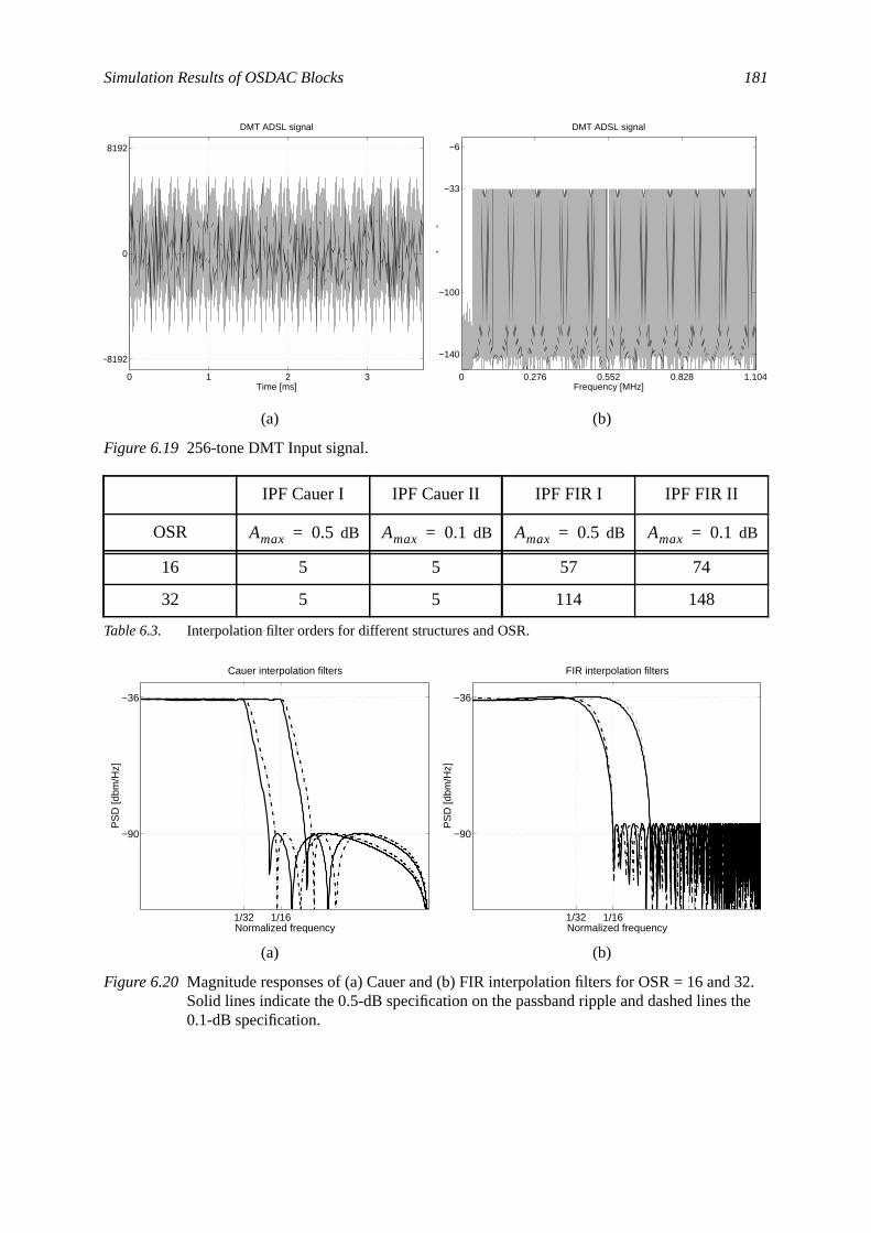
Simulation Results of OSDAC Blocks 181
32. the
(a) (b)
Figure 6.19 256-tone DMT Input signal.
IPF Cauer I IPF Cauer II IPF FIR I IPF FIR II
OSR dB dB dB dB
16 5 5 57 74
32 5 5 114 148
Table 6.3. Interpolation filter orders for different structures and OSR.
(a) (b)
Figure 6.20 Magnitude responses of (a) Cauer and (b) FIR interpolation filters for OSR = 16 andSolid lines indicate the 0.5-dB specification on the passband ripple and dashed lines0.1-dB specification.
0 1 2 3
−8192
0
8192
DMT ADSL signal
Time [ms]0 0.276 0.552 0.828 1.104
−140
−100
−33
−6
DMT ADSL signal
Pow
er [d
BF
S]
Frequency [MHz]
Amax 0.5= Amax 0.1= Amax 0.5= Amax 0.1=
1/32 1/16
−90
−36
Normalized frequency
PS
D [d
bm/H
z]
Cauer interpolation filters
1/32 1/16
−90
−36
Normalized frequency
PS
D [d
bm/H
z]
FIR interpolation filters
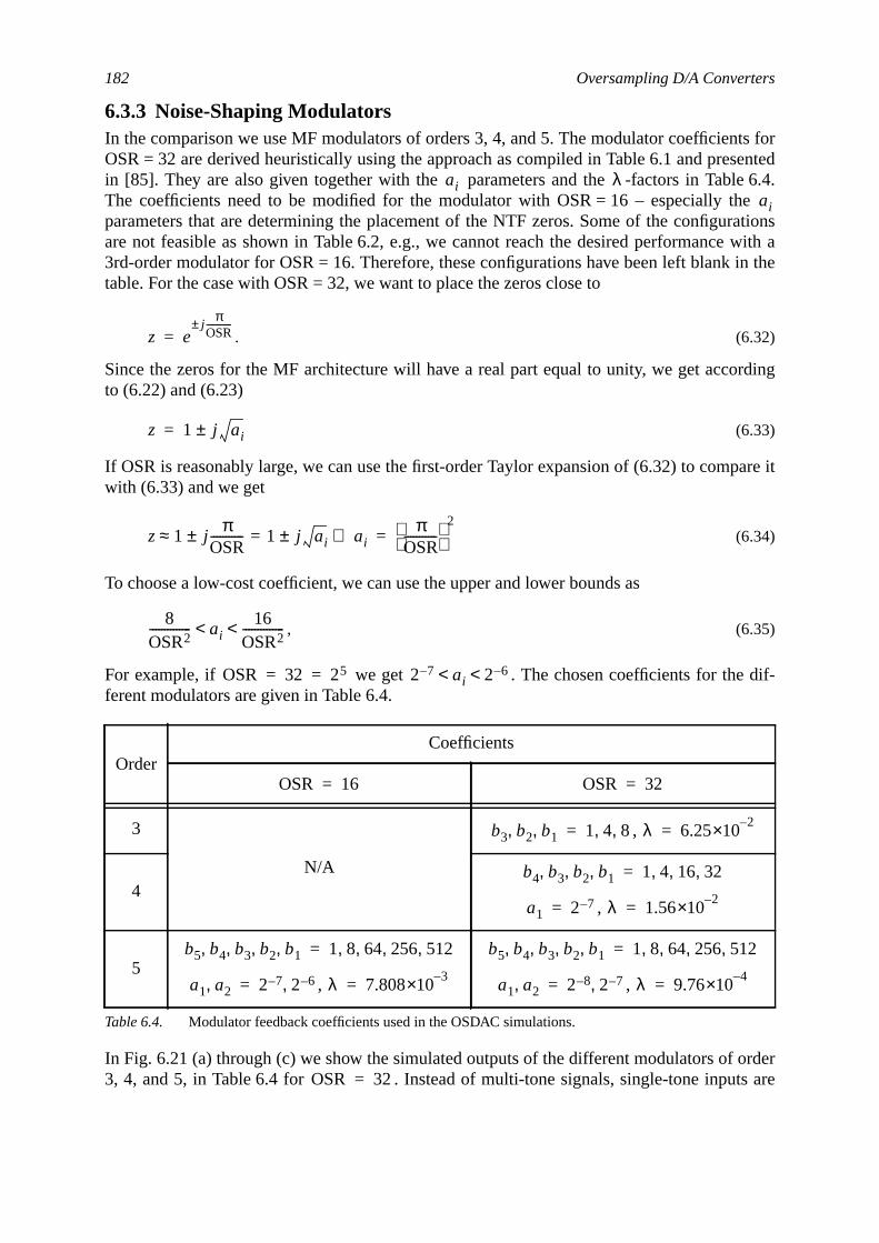
182 Oversampling D/A Converters
ts forsented
6.4.erationswith a
in the
rding
are it
if-
rderare
6.3.3 Noise-Shaping ModulatorsIn the comparison we use MF modulators of orders 3, 4, and 5. The modulator coefficienOSR = 32 are derived heuristically using the approach as compiled in Table 6.1 and prein [85]. They are also given together with the parameters and the -factors in TableThe coefficients need to be modified for the modulator with OSR = 16 – especially thparameters that are determining the placement of the NTF zeros. Some of the configuare not feasible as shown in Table 6.2, e.g., we cannot reach the desired performance3rd-order modulator for OSR = 16. Therefore, these configurations have been left blanktable. For the case with OSR = 32, we want to place the zeros close to
. (6.32)
Since the zeros for the MF architecture will have a real part equal to unity, we get accoto (6.22) and (6.23)
(6.33)
If OSR is reasonably large, we can use the first-order Taylor expansion of (6.32) to compwith (6.33) and we get
(6.34)
To choose a low-cost coefficient, we can use the upper and lower bounds as
, (6.35)
For example, if we get . The chosen coefficients for the dferent modulators are given in Table 6.4.
In Fig. 6.21 (a) through (c) we show the simulated outputs of the different modulators of o3, 4, and 5, in Table 6.4 for . Instead of multi-tone signals, single-tone inputs
OrderCoefficients
3
N/A
,
4,
5, ,
Table 6.4. Modulator feedback coefficients used in the OSDAC simulations.
ai λai
z ej
πOSR-----------±
=
z 1 j ai±=
z 1 jπ
OSR-----------±≈ 1 j ai±= ai⇒ π
OSR-----------
2=
8OSR2-------------- ai
16OSR2--------------< <
OSR 32 25= = 2 7– ai 2 6–< <
OSR 16= OSR 32=
b3 b2 b1, , 1 4 8, ,= λ 6.252–×10=
b4 b3 b2 b1, , , 1 4 16 32, , ,=
a1 2 7–= λ 1.562–×10=
b5 b4 b3 b2 b1, , , , 1 8 64 256 512, , , ,=
a1 a2, 2 7– 2 6–,= λ 7.8083–×10=
b5 b4 b3 b2 b1, , , , 1 8 64 256 512, , , ,=
a1 a2, 2 8– 2 7–,= λ 9.764–×10=
OSR 32=
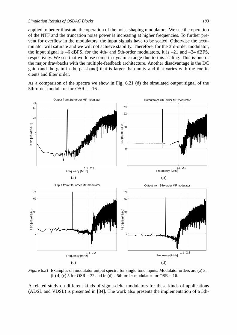
Simulation Results of OSDAC Blocks 183
rationr pre-accu-tor,
BFS,ne ofe DCoeffi-
f the
tions5th-
a) 3,
applied to better illustrate the operation of the noise shaping modulators. We see the opeof the NTF and the truncation noise power is increasing at higher frequencies. To furthevent for overflow in the modulators, the input signals have to be scaled. Otherwise themulator will saturate and we will not achieve stability. Therefore, for the 3rd-order modulathe input signal is –6 dBFS, for the 4th- and 5th-order modulators, it is –21 and –24 drespectively. We see that we loose some in dynamic range due to this scaling. This is othe major drawbacks with the multiple-feedback architecture. Another disadvantage is thgain (and the gain in the passband) that is larger than unity and that varies with the ccients and filter order.
As a comparison of the spectra we show in Fig. 6.21 (d) the simulated output signal o5th-order modulator for .
A related study on different kinds of sigma-delta modulators for these kinds of applica(ADSL and VDSL) is presented in [84]. The work also presents the implementation of a
(a) (b)
(c) (d)
Figure 6.21 Examples on modulator output spectra for single-tone inputs. Modulator orders are ((b) 4, (c) 5 for OSR = 32 and in (d) a 5th-order modulator for OSR = 16.
OSR 16=
1.1 2.2
0
38
62
74
Frequency [MHz]
PS
D [d
Bm
FS
/Hz]
Output from 3rd−order MF modulator
1.1 2.2
0
38
62
74
Frequency [MHz]
PS
D [d
Bm
FS
/Hz]
Output from 4th−order MF modulator
1.1 2.2
0
38
62
74
Frequency [MHz]
PS
D [d
Bm
FS
/Hz]
Output from 5th−order MF modulator
1.1 2.2
0
38
62
74
Frequency [MHz]
PS
D [d
Bm
FS
/Hz]
Output from 5th−order MF modulator
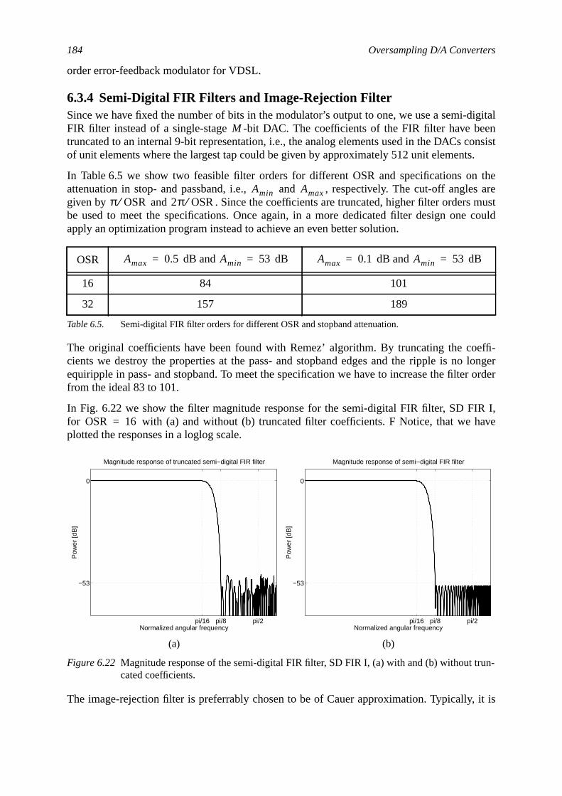
184 Oversampling D/A Converters
igitaleenonsist
ts.
thes areustcould
effi-longer
r order
R I,ve
it is
run-
order error-feedback modulator for VDSL.
6.3.4 Semi-Digital FIR Filters and Image-Rejection FilterSince we have fixed the number of bits in the modulator’s output to one, we use a semi-dFIR filter instead of a single-stage -bit DAC. The coefficients of the FIR filter have btruncated to an internal 9-bit representation, i.e., the analog elements used in the DACs cof unit elements where the largest tap could be given by approximately 512 unit elemen
In Table 6.5 we show two feasible filter orders for different OSR and specifications onattenuation in stop- and passband, i.e., and , respectively. The cut-off anglegiven by and . Since the coefficients are truncated, higher filter orders mbe used to meet the specifications. Once again, in a more dedicated filter design oneapply an optimization program instead to achieve an even better solution.
The original coefficients have been found with Remez’ algorithm. By truncating the cocients we destroy the properties at the pass- and stopband edges and the ripple is noequiripple in pass- and stopband. To meet the specification we have to increase the filtefrom the ideal 83 to 101.
In Fig. 6.22 we show the filter magnitude response for the semi-digital FIR filter, SD FIfor with (a) and without (b) truncated filter coefficients. F Notice, that we haplotted the responses in a loglog scale.
The image-rejection filter is preferrably chosen to be of Cauer approximation. Typically,
OSR dB and dB dB and dB
16 84 101
32 157 189
Table 6.5. Semi-digital FIR filter orders for different OSR and stopband attenuation.
(a) (b)
Figure 6.22 Magnitude response of the semi-digital FIR filter, SD FIR I, (a) with and (b) without tcated coefficients.
M
Amin Amaxπ OSR⁄ 2π OSR⁄
Amax 0.5= Amin 53= Amax 0.1= Amin 53=
OSR 16=
pi/16 pi/8 pi/2
−53
0
Normalized angular frequency
Pow
er [d
B]
Magnitude response of truncated semi−digital FIR filter
pi/16 pi/8 pi/2
−53
0
Normalized angular frequency
Pow
er [d
B]
Magnitude response of semi−digital FIR filter
A CMOS Current-Steering 5th-Order OSDAC for DMT-ADSL 185
n theder 1terr this
andthe
namic32 is
beenThere-dB).havete byin a
SLhoutlterThe
e to ale-hence
were
ccu-willed tobe
zgular
implemented with active RC or gm-C circuits. Since we want to keep the design effort oanalog filter at a minimum and therefore the order of the analog filter should be of the oror 2. Without the semi-digital FIR filter, we would require very high continuous-time filorders due to the high truncation noise power. For a Cauer approximation of the filtewould result in orders of at least 6 or 7 as discussed in Chapter 3.
6.4 A CMOS Current-Steering 5th-OrderOSDAC for DMT-ADSL
It has been found [85, 92, 93] that the ADSL specification will not be met with the 3rd4th order modulators and only nearly met with the 5th-order modulator. This is due torequired downscaling of the input signal, since we are not able to reach the desired dyrange with the chosen single-bit output. Further, an oversampling ratio of at leastrequired to allow a feasible implementation of a modulator with a single-bit output.
Once again, notice that in this work no co-optimization of the passband behavior hastaken into account. Instead we sum up the total loss at the passband edge of all filters.fore, we have chosen the passband ripple from the interpolation to be small (Then we let, due to the coarse quantization of the coefficients, the semi-digital FIR filtera rather high ripple in the passband. (The specification allows that the carriers fluctuaapproximately 3 dB). With an optimization toolbox we can generate filter coefficientssmarter way so that the behavior within the passband is much more controlled.
In this section we present the design of a 14-bit 5-V 0.6- mCMOS OSDAC for DMT-ADapplications [85, 92, 93]. The oversampling ratio is 32. The OSDAC is implemented witinterpolation filters or an analog filter. The modulator order is 5 and the semi-digital FIR fihas 219 taps. In this section we briefly overview the design of the semi-digital FIR filter.analog filter was not implemented since it would require too large on-chip capacitors duhigh output DC current from the semi-digital FIR filter. Secondly, the OSDAC was impmented to meet an older ADSL specification than the one presented in Chapter 1 andsome specification values on the filter seem somewhat misplaced.
6.4.1 Semi-Digital FIR FilterSince unit elements are used in the layout, the coefficients of the semi-digital FIR filtertruncated according to the formula
, (6.36)
where is a gain value which determines the size of the truncation error. With higher aracy, , the errors in the filter’s frequency response will be smaller, but the chip areaincrease, since with a higher we need more unit elements. The FIR filter was designmeet a specfication where the cut-off frequency was chosen to
MHz which is slightly higher than the signal bandwidth of 1.104 MHto cover for the effects due to the truncation of the coefficients. Using the normalized anfrequency the specification on the filter is
Amax 0.1=
ai Jmax ai
min ai-------------------⋅ 0.5 ai sgn⋅+=
JJ
J
f c 1.15 f N⋅ 1.27≈=
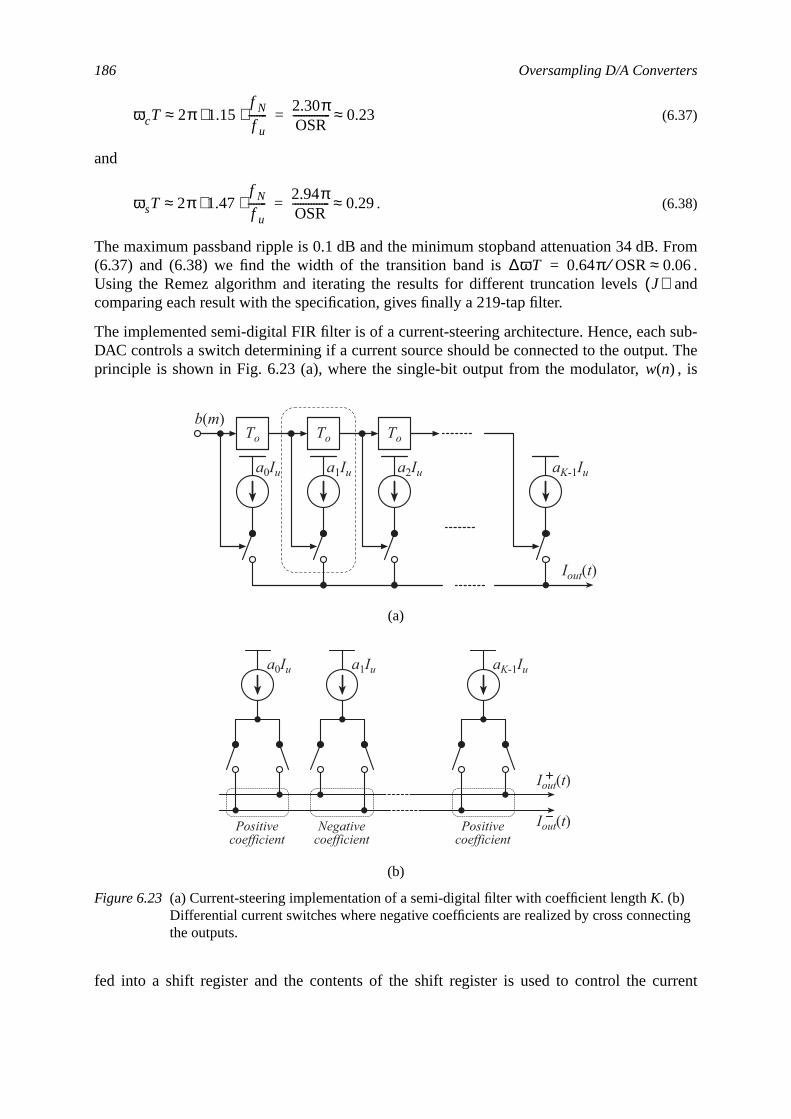
186 Oversampling D/A Converters
From.
and
sub-t. The, is
rrent
cting
(6.37)
and
. (6.38)
The maximum passband ripple is 0.1 dB and the minimum stopband attenuation 34 dB.(6.37) and (6.38) we find the width of the transition band isUsing the Remez algorithm and iterating the results for different truncation levelscomparing each result with the specification, gives finally a 219-tap filter.
The implemented semi-digital FIR filter is of a current-steering architecture. Hence, eachDAC controls a switch determining if a current source should be connected to the outpuprinciple is shown in Fig. 6.23 (a), where the single-bit output from the modulator,
fed into a shift register and the contents of the shift register is used to control the cu
(a)
(b)
Figure 6.23 (a) Current-steering implementation of a semi-digital filter with coefficient lengthK. (b)Differential current switches where negative coefficients are realized by cross connethe outputs.
ωcT 2π 1.15f N
f u-------⋅ ⋅≈ 2.30π
OSR-------------- 0.23≈=
ωsT 2π 1.47f N
f u-------⋅ ⋅≈ 2.94π
OSR-------------- 0.29≈=
∆ωT 0.64π OSR⁄ 0.06≈=J( )
w n( )
To To To
a0Iu a1Iu a2Iu aK-1Iu
b(m)
Iout(t)
Iout(t)
Iout(t)
a0Iu a1Iu aK-1Iu
Negativecoefficient
Positivecoefficient
Positivecoefficient
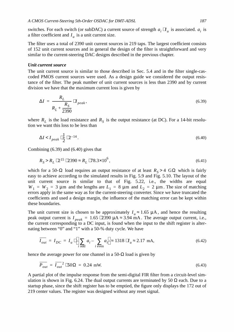
A CMOS Current-Steering 5th-Order OSDAC for DMT-ADSL 187
. is
nsistsvery
-cas-t resis-urrent
solu-
irlyof theualngted thewithin
lting.e.,lter-
im-
out of
switches. For each switch (or subDAC) a current source of strength is associateda filter coefficient and is a unit current size.
The filter uses a total of 2390 unit current sources in 219 taps. The largest coefficient coof 152 unit current sources and in general the design of the filter is straightforward andsimilar to the current-steering DAC designs described in the previous chapter.
Unit current sourceThe unit current source is similar to those described in Sec. 5.4 and in the filter singlecoded PMOS current sources were used. As a design guide we considered the outputance of the filter. The peak number of unit current sources is less than 2390 and by cdivision we have that the maximum current loss is given by
, (6.39)
where is the load resistance and is the output resistance (at DC). For a 14-bit retion we want this loss to be less than
. (6.40)
Combining (6.39) and (6.40) gives that
, (6.41)
which for a 50- load requires an output resistance of at least which is faeasy to achieve according to the simulated results in Fig. 5.9 and Fig. 5.10. The layoutunit current source is similar to that of Fig. 5.22, i.e., the widths are eq
and the lengths are and . The size of matchierrors apply in the same way as for the current-steering converter. Since we have truncacoefficients and used a design margin, the influence of the matching error can be keptthese boundaries.
The unit current size is chosen to be approximately , and hence the resupeak output current is . The average output current, ithe current corresponding to a DC input, is found when the input to the shift register is anating between “0” and “1” with a 50-% duty cycle. We have
mA, (6.42)
hence the average power for one channel in a 50-Ω load is given by
mW. (6.43)
A partial plot of the impulse response from the semi-digital FIR filter from a circuit-level sulation is shown in Fig. 6.24. The dual output currents are terminated by 50Ω each. Due to astartup phase, since the shift register has to be emptied, the figure only displays the 172219 center values. The register was designed without any reset signal.
ai I u⋅ aiI u
∆IRL
RL
RS
2390------------+
------------------------- I peak⋅=
RL RS
∆I I peak12--- 2 14–⋅ ⋅<
RS RL 215 2390⋅ ⋅ RL 78.36×10⋅≈>
Ω RS 4> GΩ
W1 W2 3 µm= = L1 8 µm= L2 2 µm=
I u 1.65 µA≈I peak 1.65 2390µA⋅ 3.94 mA≈=
I out I DC I u aii odd∑ ai
i even∑–
⋅ 1318 I u⋅ 2.17≈ ≈= =
Pout I out2 50Ω⋅ 0.24= =
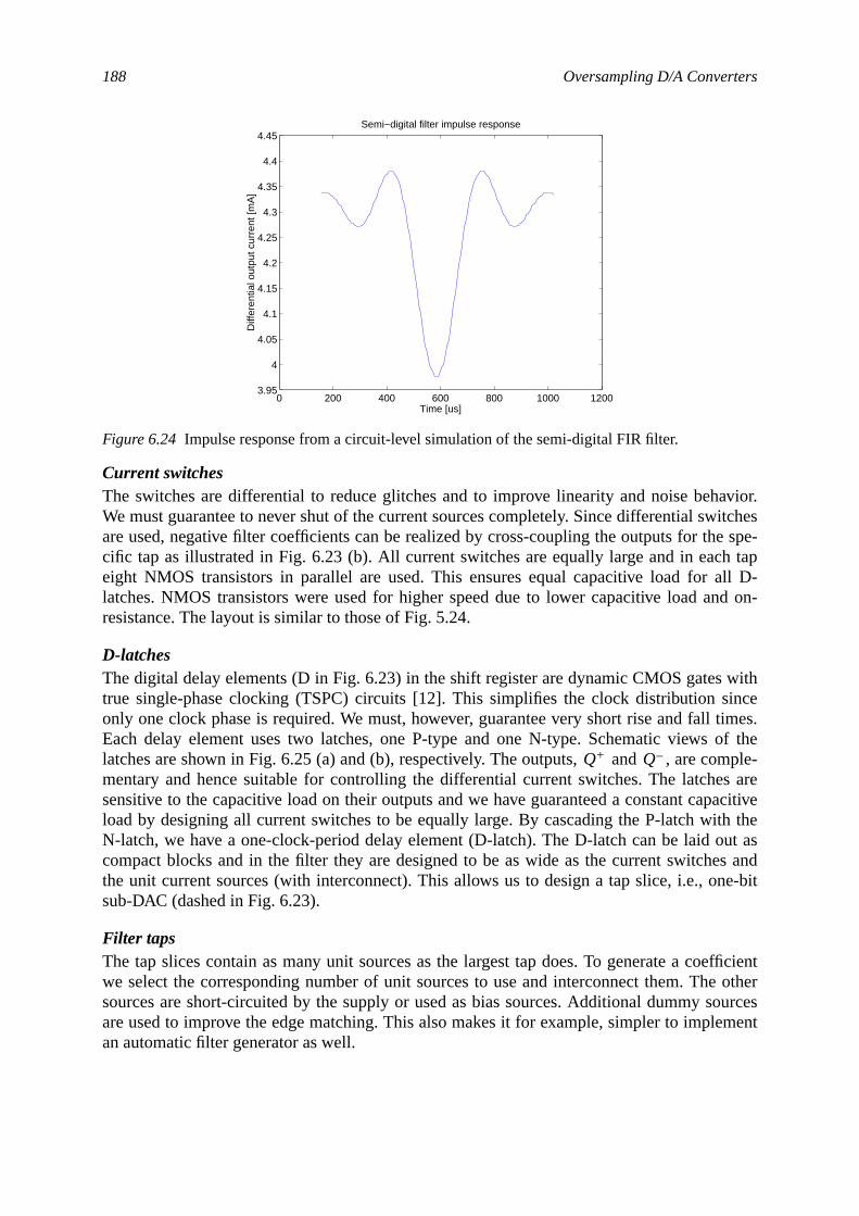
188 Oversampling D/A Converters
avior.itchese spe-
tapll D-d on-
withincetimes.of themple-s areacitive
h theut ass and
ne-bit
efficientother
ourcesment
Current switchesThe switches are differential to reduce glitches and to improve linearity and noise behWe must guarantee to never shut of the current sources completely. Since differential sware used, negative filter coefficients can be realized by cross-coupling the outputs for thcific tap as illustrated in Fig. 6.23 (b). All current switches are equally large and in eacheight NMOS transistors in parallel are used. This ensures equal capacitive load for alatches. NMOS transistors were used for higher speed due to lower capacitive load anresistance. The layout is similar to those of Fig. 5.24.
D-latchesThe digital delay elements (D in Fig. 6.23) in the shift register are dynamic CMOS gatestrue single-phase clocking (TSPC) circuits [12]. This simplifies the clock distribution sonly one clock phase is required. We must, however, guarantee very short rise and fallEach delay element uses two latches, one P-type and one N-type. Schematic viewslatches are shown in Fig. 6.25 (a) and (b), respectively. The outputs, and , are comentary and hence suitable for controlling the differential current switches. The latchesensitive to the capacitive load on their outputs and we have guaranteed a constant capload by designing all current switches to be equally large. By cascading the P-latch witN-latch, we have a one-clock-period delay element (D-latch). The D-latch can be laid ocompact blocks and in the filter they are designed to be as wide as the current switchethe unit current sources (with interconnect). This allows us to design a tap slice, i.e., osub-DAC (dashed in Fig. 6.23).
Filter tapsThe tap slices contain as many unit sources as the largest tap does. To generate a cowe select the corresponding number of unit sources to use and interconnect them. Thesources are short-circuited by the supply or used as bias sources. Additional dummy sare used to improve the edge matching. This also makes it for example, simpler to implean automatic filter generator as well.
Figure 6.24 Impulse response from a circuit-level simulation of the semi-digital FIR filter.
0 200 400 600 800 1000 12003.95
4
4.05
4.1
4.15
4.2
4.25
4.3
4.35
4.4
4.45Semi−digital filter impulse response
Diff
eren
tial o
utpu
t cur
rent
[mA
]
Time [us]
Q+ Q–
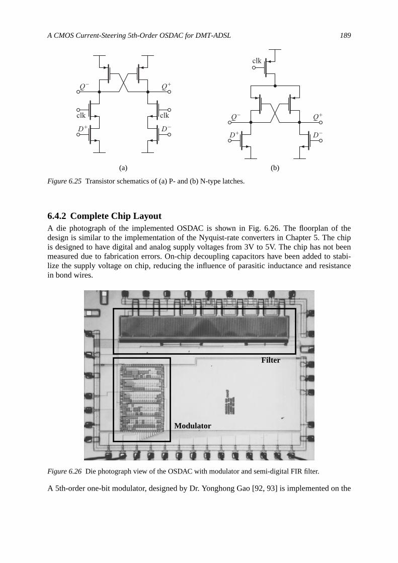
A CMOS Current-Steering 5th-Order OSDAC for DMT-ADSL 189
thechipbeenstabi-
tance
n the
6.4.2 Complete Chip LayoutA die photograph of the implemented OSDAC is shown in Fig. 6.26. The floorplan ofdesign is similar to the implementation of the Nyquist-rate converters in Chapter 5. Theis designed to have digital and analog supply voltages from 3V to 5V. The chip has notmeasured due to fabrication errors. On-chip decoupling capacitors have been added tolize the supply voltage on chip, reducing the influence of parasitic inductance and resisin bond wires.
A 5th-order one-bit modulator, designed by Dr. Yonghong Gao [92, 93] is implemented o
(a) (b)
Figure 6.25 Transistor schematics of (a) P- and (b) N-type latches.
Figure 6.26 Die photograph view of the OSDAC with modulator and semi-digital FIR filter.
clk clk
Q Q
D D
clk
Q Q
D D
Filter
Modulator

190 Oversampling D/A Converters
on isduce
ageandrrentlayersgister.
chip. Its core size is approximately and the approximate power consumpti92 mW at a clock frequency of 71 MHz and 3-V supply. To save hardware and to repower dissipation the modulator’s coefficients have been scaled internally.
The core area of the semi-digital FIR filter is approximately . The averpower dissipation for the filter is approximately 6 mW at 71 MHz and with a 3-V analogdigital supply. A higher-layer metal plate is covering the current sources to provide the cusources with the positive analog supply. N- and P-diffusion layers are used as shieldingto decrease substrate coupling between the analog current sources and the digital shift re
1.2 0.8× µm2
3.2 0.5× µm2
mainlyout-
gnal-whichsfer
rs doto the
ncence.onetized,ll still
errorsre arecases;tching
one ising ancali-get
ise or
7 Special Techniques forEnhanced D/A Conversion
7.1 IntroductionIn the previous sections we have discussed implementation aspects and properties ofcurrent-steering DACs. We have found that the major limitations on performance are theput impedance, matching errors, and noise. A finite output impedance will give a sidependent settling time as well as a signal-dependent current loss through the DACresults in distortion. The matching errors are static and they will influence the DC trancharacteristics. With a dual DAC output the even-order distortion due to matching erronot cancel eachother. This is, however, the case for the even-order terms arising duefinite output impedance. With an output buffer providing the DAC with a low-impedanode, i.e., virtual ground, practically eliminates the problem with limited output impedaTherefore most effort should be put on minimizing the matching errors. Typically this is dthrough careful layout with special techniques, such as using unit elements, interdigicommon-centroid and dummy elements for improved edge matching. However, there wibe matching errors that influence the achievable performance.
In this chapter we discuss some different methods to reduce the effect of the matchingby using proposed algorithms and other special techniques in the digital domain. Theseveral different approaches to improve performance and we divide them into threeinverse functions (Sec. 7.2), element calibration (Sec. 7.3), and dynamic element ma(DEM) techniques (Sec. 7.4).
The inverse-function methods presented in Sec. 7.2 require two important parameters:knowledge about the nature of the nonlinearity and the second is a feedback loop includADC or similar. For the calibration and DEM techniques this is not needed. The elementbration technique aims on adjusting the size of the elements in the DAC. With DEM wethe average of the signal-dependent errors and will transform into signal-independent nooffset.
191
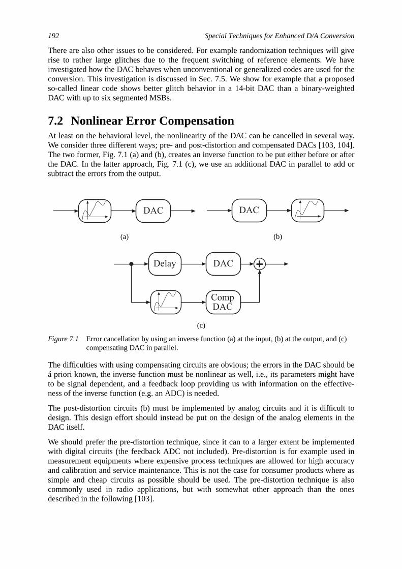
192 Special Techniques for Enhanced D/A Conversion
ill givehavefor theposedhted
way.104].
r afterd or
ld behavetive-
lt toin the
entedd inccuracyere as
is alsoones
(c)
There are also other issues to be considered. For example randomization techniques wrise to rather large glitches due to the frequent switching of reference elements. Weinvestigated how the DAC behaves when unconventional or generalized codes are usedconversion. This investigation is discussed in Sec. 7.5. We show for example that a proso-called linear code shows better glitch behavior in a 14-bit DAC than a binary-weigDAC with up to six segmented MSBs.
7.2 Nonlinear Error CompensationAt least on the behavioral level, the nonlinearity of the DAC can be cancelled in severalWe consider three different ways; pre- and post-distortion and compensated DACs [103,The two former, Fig. 7.1 (a) and (b), creates an inverse function to be put either before othe DAC. In the latter approach, Fig. 7.1 (c), we use an additional DAC in parallel to adsubtract the errors from the output.
The difficulties with using compensating circuits are obvious; the errors in the DAC shouá priori known, the inverse function must be nonlinear as well, i.e., its parameters mightto be signal dependent, and a feedback loop providing us with information on the effecness of the inverse function (e.g. an ADC) is needed.
The post-distortion circuits (b) must be implemented by analog circuits and it is difficudesign. This design effort should instead be put on the design of the analog elementsDAC itself.
We should prefer the pre-distortion technique, since it can to a larger extent be implemwith digital circuits (the feedback ADC not included). Pre-distortion is for example usemeasurement equipments where expensive process techniques are allowed for high aand calibration and service maintenance. This is not the case for consumer products whsimple and cheap circuits as possible should be used. The pre-distortion techniquecommonly used in radio applications, but with somewhat other approach than thedescribed in the following [103].
(a) (b)
(c)
Figure 7.1 Error cancellation by using an inverse function (a) at the input, (b) at the output, andcompensating DAC in parallel.
DAC DAC
DAC
CompDAC
Delay
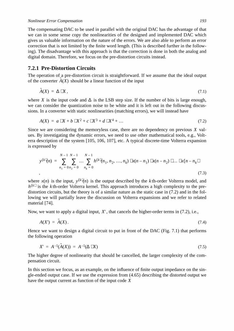
Nonlinear Error Compensation 193
f thatwhicherror
ow-g and
utput
ugh,cus-
val-, Volt-sion
andpre-e fol-ated
.,
ms
com-
e sin-ut we
The compensating DAC to be used in parallel with the original DAC has the advantage owe can in some sense copy the nonlinearities of the designed and implemented DACgives us valuable information on the nature of the errors. We are also able to perform ancorrection that is not limited by the finite word length. (This is described further in the folling). The disadvantage with this approach is that the correction is done in both the analodigital domain. Therefore, we focus on the pre-distortion circuits instead.
7.2.1 Pre-Distortion CircuitsThe operation of a pre-distortion circuit is straightforward. If we assume that the ideal oof the converter should be a linear function of the input
, (7.1)
where is the input code and is the LSB step size. If the number of bits is large enowe can consider the quantization noise to be white and it is left out in the following dissions. In a converter with static nonlinearities (matching errors), we will instead have
(7.2)
Since we are considering the memoryless case, there are no dependency on previousues. By investigating the dynamic errors, we need to use other mathematical tools, e.g.erra description of the system [105, 106, 107], etc. A typical discrete-time Volterra expanis expressed by
, (7.3)
where is the input, is the output described by the th-order Volterra model,is the th-order Volterra kernel. This approach introduces a high complexity to the
distortion circuits, but the theory is of a similar nature as the static case in (7.2) and in thlowing we will partially leave the discussion on Volterra expansions and we refer to relmaterial [74].
Now, we want to apply a digital input, , that cancels the higher-order terms in (7.2), i.e
. (7.4)
Hence we want to design a digital circuit to put in front of the DAC (Fig. 7.1) that perforthe following operation
(7.5)
The higher degree of nonlinearity that should be cancelled, the larger complexity of thepensation circuit.
In this section we focus, as an example, on the influence of finite output impedance on thgle-ended output case. If we use the expression from (4.65) describing the distorted outphave the output current as function of the input code
A X( )
A X( ) ∆ X⋅=
X ∆
A X( ) a X⋅ b X2⋅ c X3⋅ d X4⋅ …+ + + +=
X
y k( ) n( ) … h k( ) n1 n2 … nk, , ,( ) x n n1–( ) x n n2–( ) … x n nk–( )⋅ ⋅ ⋅ ⋅nk 0=
N 1–
∑n2 0=
N 1–
∑n1 0=
N 1–
∑=
x n( ) y k( ) n( ) kh k( ) k
X'
A X'( ) A X( )=
X' A 1– A X( )( ) A 1– ∆ X⋅( )= =
X
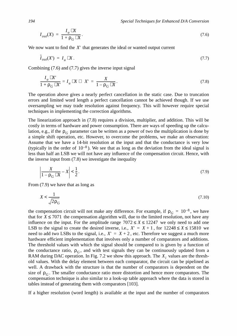
194 Special Techniques for Enhanced D/A Conversion
catione useecial
l becalcu-e byation:y lowal iswith
aveanyonewemoretions.n ofom aesh-ed asn thes. Thered in
ators
. (7.6)
We now want to find the that generates the ideal or wanted output current
. (7.7)
Combining (7.6) and (7.7) gives the inverse input signal
. (7.8)
The operation above gives a nearly perfect cancellation in the static case. Due to trunerrors and limited word length a perfect cancellation cannot be achieved though. If woversampling we may trade resolution against frequency. This will however require sptechniques in implementing the correction algorithms.
The linearization approach in (7.8) requires a division, multiplier, and addition. This wilcostly in terms of hardware and power consumption. There are ways of speeding up thelation, e.g., if the parameter can be written as a power of two the multiplication is dona simple shift operation, etc. However, to overcome the problems, we make an observAssume that we have a 14-bit resolution at the input and that the conductance is ver(typically in the order of ). We see that as long as the deviation from the ideal signless than half an LSB we will not have any influence of the compensation circuit. Hence,the inverse input from (7.8) we investigate the inequality
. (7.9)
From (7.9) we have that as long as
(7.10)
the compensation circuit will not make any difference. For example, if , we hthat for the compensation algorithm will, due to the limited resolution, not haveinfluence on the input. For the amplitude range we only need to addLSB to the signal to create the desired inverse, i.e., , forneed to add two LSBs to the signal, i.e., , etc. Therefore we suggest a muchhardware efficient implementation that involves only a number of comparators and addiThe threshold values with which the signal should be compared to is given by a functiothe conductance ratio, , and with test signals they can be continuously updated frRAM during DAC operation. In Fig. 7.2 we show this approach. The values are the throld values. With the delay element between each comparator, the circuit can be pipelinwell. A drawback with the structure is that the number of comparators is dependent osize of . The smaller conductance ratio more distortion and hence more comparatorcompensation technique is also similar to a look-up table approach where the data is stotables instead of generating them with comparators [103].
If a higher resolution (word length) is available at the input and the number of compar
I out X( )I u X⋅
1 ρG X⋅+------------------------=
X'
I out X'( ) I u X⋅=
I u X'⋅1 ρG X'⋅+------------------------- I u X⋅= X'⇒ X
1 ρG X⋅–------------------------=
ρG
10 8–
X1 ρG X⋅–------------------------ X–
12---<
X1
2ρG
--------------<
ρG 10 8–=X 7071≤
7072 X 12247≤ ≤X' X 1+= 12248 X 15810≤ ≤
X' X 2+=
ρGXi
ρG
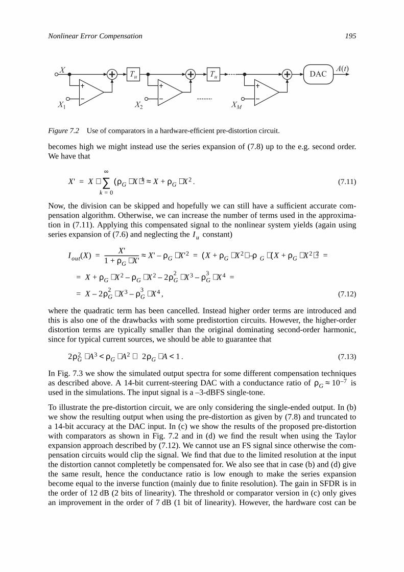
Nonlinear Error Compensation 195
order.
com-xima-sing
ed andorderonic,
iquesis
n (b)ted tortion
aylore com-nputd) giveansionis inivesn be
becomes high we might instead use the series expansion of (7.8) up to the e.g. secondWe have that
. (7.11)
Now, the division can be skipped and hopefully we can still have a sufficient accuratepensation algorithm. Otherwise, we can increase the number of terms used in the approtion in (7.11). Applying this compensated signal to the nonlinear system yields (again useries expansion of (7.6) and neglecting the constant)
, (7.12)
where the quadratic term has been cancelled. Instead higher order terms are introducthis is also one of the drawbacks with some predistortion circuits. However, the higher-distortion terms are typically smaller than the original dominating second-order harmsince for typical current sources, we should be able to guarantee that
. (7.13)
In Fig. 7.3 we show the simulated output spectra for some different compensation technas described above. A 14-bit current-steering DAC with a conductance ratio ofused in the simulations. The input signal is a –3-dBFS single-tone.
To illustrate the pre-distortion circuit, we are only considering the single-ended output. Iwe show the resulting output when using the pre-distortion as given by (7.8) and truncaa 14-bit accuracy at the DAC input. In (c) we show the results of the proposed pre-distowith comparators as shown in Fig. 7.2 and in (d) we find the result when using the Texpansion approach described by (7.12). We cannot use an FS signal since otherwise thpensation circuits would clip the signal. We find that due to the limited resolution at the ithe distortion cannot completetly be compensated for. We also see that in case (b) and (the same result, hence the conductance ratio is low enough to make the series expbecome equal to the inverse function (mainly due to finite resolution). The gain in SFDRthe order of 12 dB (2 bits of linearity). The threshold or comparator version in (c) only gan improvement in the order of 7 dB (1 bit of linearity). However, the hardware cost ca
Figure 7.2 Use of comparators in a hardware-efficient pre-distortion circuit.
X1
X Tu Tu DAC
X2 XM
A(t)
X' X ρG X⋅( )k
k 0=
∞
∑⋅ X ρG X2⋅+≈=
I u
I out X( )X'
1 ρG X'⋅+------------------------- X' ρG X'2⋅–≈ X ρG X2⋅+( ) ρG X ρG X2⋅+( )2⋅–= = =
X ρG X2⋅ ρG X2⋅– 2ρG2
X3⋅– ρG3
X4⋅–+= =
X 2ρG2
X3⋅– ρG3
X4⋅–=
2ρG2 A3⋅ ρG A2⋅< 2ρG A⋅ 1<⇒
ρG 10 7–≈
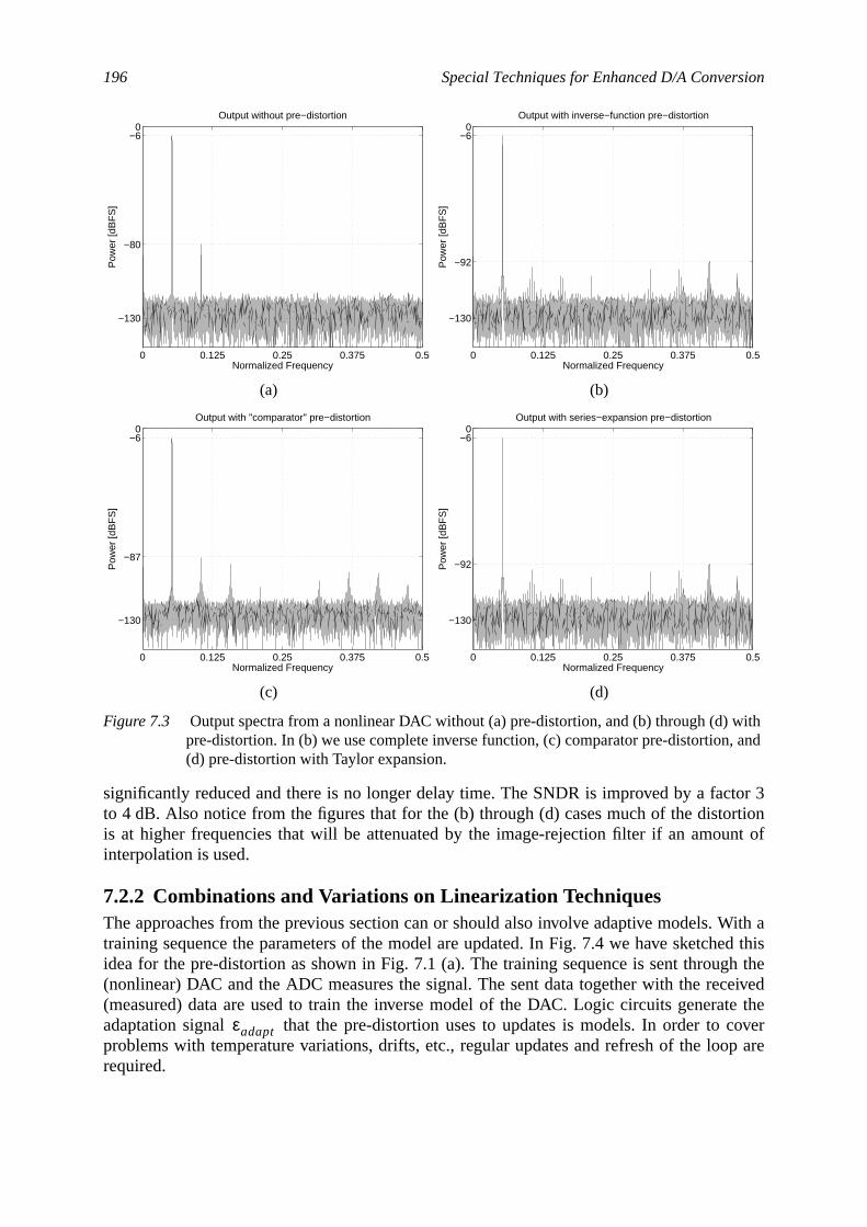
196 Special Techniques for Enhanced D/A Conversion
tor 3rtionnt of
With aed thish theeivedte thecoverp are
ith, and
significantly reduced and there is no longer delay time. The SNDR is improved by a facto 4 dB. Also notice from the figures that for the (b) through (d) cases much of the distois at higher frequencies that will be attenuated by the image-rejection filter if an amouinterpolation is used.
7.2.2 Combinations and Variations on Linearization TechniquesThe approaches from the previous section can or should also involve adaptive models.training sequence the parameters of the model are updated. In Fig. 7.4 we have sketchidea for the pre-distortion as shown in Fig. 7.1 (a). The training sequence is sent throug(nonlinear) DAC and the ADC measures the signal. The sent data together with the rec(measured) data are used to train the inverse model of the DAC. Logic circuits generaadaptation signal that the pre-distortion uses to updates is models. In order toproblems with temperature variations, drifts, etc., regular updates and refresh of the loorequired.
(a) (b)
(c) (d)
Figure 7.3 Output spectra from a nonlinear DAC without (a) pre-distortion, and (b) through (d) wpre-distortion. In (b) we use complete inverse function, (c) comparator pre-distortion(d) pre-distortion with Taylor expansion.
0 0.125 0.25 0.375 0.5
−130
−80
−60
Output without pre−distortionP
ower
[dB
FS
]
Normalized Frequency0 0.125 0.25 0.375 0.5
−130
−92
−60
Output with inverse−function pre−distortion
Pow
er [d
BF
S]
Normalized Frequency
0 0.125 0.25 0.375 0.5
−130
−87
−60
Output with "comparator" pre−distortion
Pow
er [d
BF
S]
Normalized Frequency0 0.125 0.25 0.375 0.5
−130
−92
−60
Output with series−expansion pre−distortion
Pow
er [d
BF
S]
Normalized Frequency
εadapt
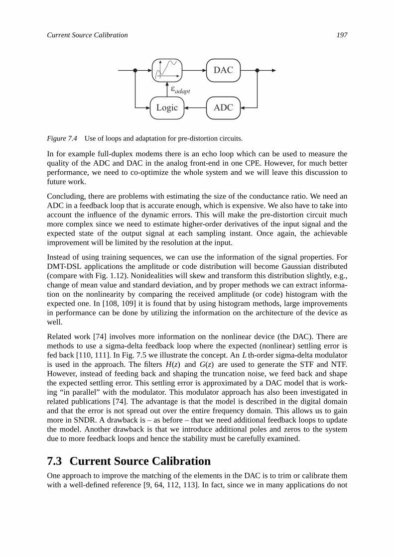
Current Source Calibration 197
re thetter
ion to
ed ane intouchd the
evable
s. Foruted.g.,forma-theentse as
arerror islatorNTF.shapeork-d inmaingain
pdateystem
themnot
In for example full-duplex modems there is an echo loop which can be used to measuquality of the ADC and DAC in the analog front-end in one CPE. However, for much beperformance, we need to co-optimize the whole system and we will leave this discussfuture work.
Concluding, there are problems with estimating the size of the conductance ratio. We neADC in a feedback loop that is accurate enough, which is expensive. We also have to takaccount the influence of the dynamic errors. This will make the pre-distortion circuit mmore complex since we need to estimate higher-order derivatives of the input signal anexpected state of the output signal at each sampling instant. Once again, the achiimprovement will be limited by the resolution at the input.
Instead of using training sequences, we can use the information of the signal propertieDMT-DSL applications the amplitude or code distribution will become Gaussian distrib(compare with Fig. 1.12). Nonidealities will skew and transform this distribution slightly, echange of mean value and standard deviation, and by proper methods we can extract intion on the nonlinearity by comparing the received amplitude (or code) histogram withexpected one. In [108, 109] it is found that by using histogram methods, large improvemin performance can be done by utilizing the information on the architecture of the devicwell.
Related work [74] involves more information on the nonlinear device (the DAC). Theremethods to use a sigma-delta feedback loop where the expected (nonlinear) settling efed back [110, 111]. In Fig. 7.5 we illustrate the concept. An th-order sigma-delta moduis used in the approach. The filters and are used to generate the STF andHowever, instead of feeding back and shaping the truncation noise, we feed back andthe expected settling error. This settling error is approximated by a DAC model that is wing “in parallel” with the modulator. This modulator approach has also been investigaterelated publications [74]. The advantage is that the model is described in the digital doand that the error is not spread out over the entire frequency domain. This allows us tomore in SNDR. A drawback is – as before – that we need additional feedback loops to uthe model. Another drawback is that we introduce additional poles and zeros to the sdue to more feedback loops and hence the stability must be carefully examined.
7.3 Current Source CalibrationOne approach to improve the matching of the elements in the DAC is to trim or calibratewith a well-defined reference [9, 64, 112, 113]. In fact, since we in many applications do
Figure 7.4 Use of loops and adaptation for pre-distortion circuits.
DAC
ADCLogic
eadapt
LH z( ) G z( )
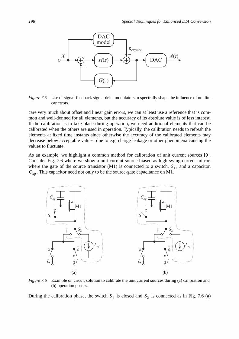
198 Special Techniques for Enhanced D/A Conversion
is com-erest.an besh thets maysing the
[9].irror,
acitor,
.6 (a)
onlin-
and
care very much about offset and linear gain errors, we can at least use a reference thatmon and well-defined for all elements, but the accuracy of its absolute value is of less intIf the calibration is to take place during operation, we need additional elements that ccalibrated when the others are used in operation. Typically, the calibration needs to refreelements at fixed time instants since otherwise the accuracy of the calibrated elemendecrease below acceptable values, due to e.g. charge leakage or other phenomena cauvalues to fluctuate.
As an example, we highlight a common method for calibration of unit current sourcesConsider Fig. 7.6 where we show a unit current source biased as high-swing current mwhere the gate of the source transistor (M1) is connected to a switch, , and a cap
. This capacitor need not only to be the source-gate capacitance on M1.
During the calibration phase, the switch is closed and is connected as in Fig. 7
Figure 7.5 Use of signal-feedback sigma-delta modulators to spectrally shape the influence of near errors.
(a) (b)
Figure 7.6 Example on circuit solution to calibrate the unit current sources during (a) calibration(b) operation phases.
H(z)
G(z)
DAC
DACmodel
eexpect
X A(t)
S1Csg
I+ I-
f fIref
M1
Csg
S1
S2
I+ I-
f fIref
M1
Csg
S1
S2
S1 S2
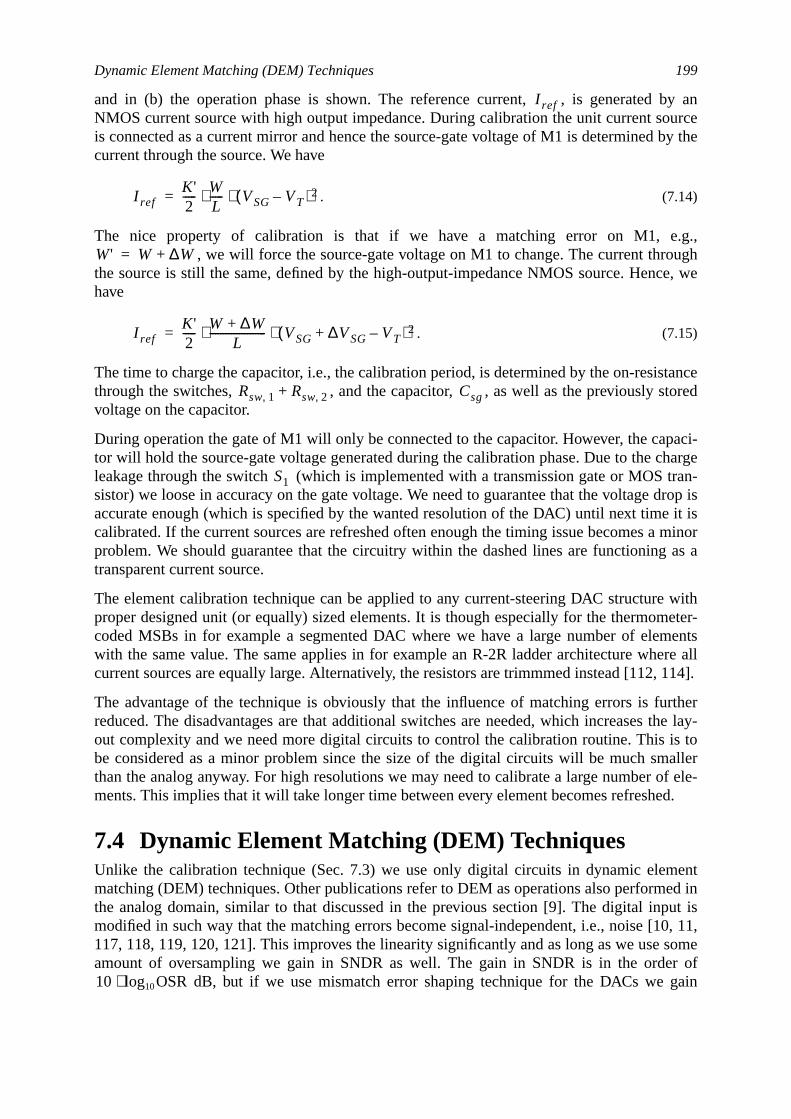
Dynamic Element Matching (DEM) Techniques 199
by anurceby the
.g.,ughe, we
stanceored
paci-hargetran-drop isit isminoras a
witheter-
mentsere all, 114].
rtherthe lay-is toaller
of ele-ed.
ented inut is0, 11,somer ofain
and in (b) the operation phase is shown. The reference current, , is generatedNMOS current source with high output impedance. During calibration the unit current sois connected as a current mirror and hence the source-gate voltage of M1 is determinedcurrent through the source. We have
. (7.14)
The nice property of calibration is that if we have a matching error on M1, e, we will force the source-gate voltage on M1 to change. The current thro
the source is still the same, defined by the high-output-impedance NMOS source. Henchave
. (7.15)
The time to charge the capacitor, i.e., the calibration period, is determined by the on-resithrough the switches, , and the capacitor, , as well as the previously stvoltage on the capacitor.
During operation the gate of M1 will only be connected to the capacitor. However, the cator will hold the source-gate voltage generated during the calibration phase. Due to the cleakage through the switch (which is implemented with a transmission gate or MOSsistor) we loose in accuracy on the gate voltage. We need to guarantee that the voltageaccurate enough (which is specified by the wanted resolution of the DAC) until next timecalibrated. If the current sources are refreshed often enough the timing issue becomes aproblem. We should guarantee that the circuitry within the dashed lines are functioningtransparent current source.
The element calibration technique can be applied to any current-steering DAC structureproper designed unit (or equally) sized elements. It is though especially for the thermomcoded MSBs in for example a segmented DAC where we have a large number of elewith the same value. The same applies in for example an R-2R ladder architecture whcurrent sources are equally large. Alternatively, the resistors are trimmmed instead [112
The advantage of the technique is obviously that the influence of matching errors is fureduced. The disadvantages are that additional switches are needed, which increasesout complexity and we need more digital circuits to control the calibration routine. Thisbe considered as a minor problem since the size of the digital circuits will be much smthan the analog anyway. For high resolutions we may need to calibrate a large numberments. This implies that it will take longer time between every element becomes refresh
7.4 Dynamic Element Matching (DEM) TechniquesUnlike the calibration technique (Sec. 7.3) we use only digital circuits in dynamic elemmatching (DEM) techniques. Other publications refer to DEM as operations also performthe analog domain, similar to that discussed in the previous section [9]. The digital inpmodified in such way that the matching errors become signal-independent, i.e., noise [1117, 118, 119, 120, 121]. This improves the linearity significantly and as long as we useamount of oversampling we gain in SNDR as well. The gain in SNDR is in the orde
dB, but if we use mismatch error shaping technique for the DACs we g
I ref
I refK'2----- W
L----- VSG VT–( )2⋅ ⋅=
W' W ∆W+=
I refK'2----- W ∆W+
L--------------------- VSG ∆VSG VT–+( )2⋅ ⋅=
Rsw 1, Rsw 2,+ Csg
S1
10 OSRlog10⋅
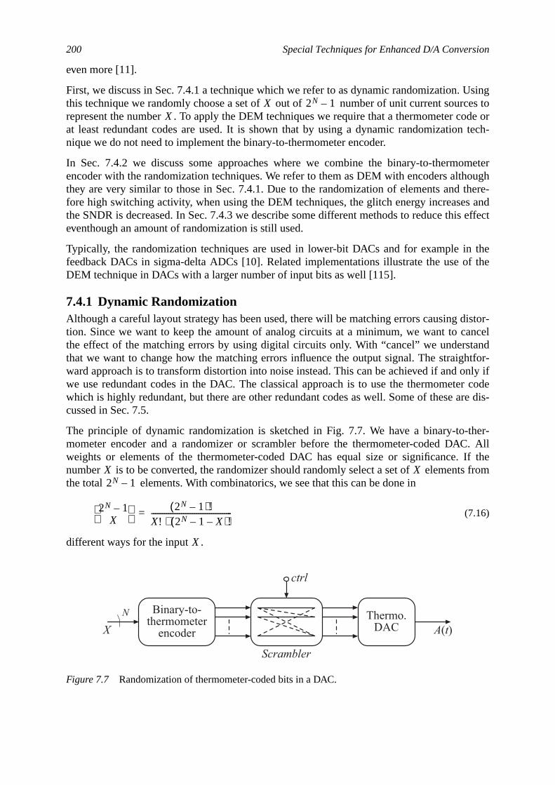
200 Special Techniques for Enhanced D/A Conversion
Usinges toode or
tech-
ometerough
there-and
s effect
thef the
distor-ncel
andhtfor-nly ifr codere dis-
ther-C. AllIf thes from
even more [11].
First, we discuss in Sec. 7.4.1 a technique which we refer to as dynamic randomization.this technique we randomly choose a set of out of number of unit current sourcrepresent the number . To apply the DEM techniques we require that a thermometer cat least redundant codes are used. It is shown that by using a dynamic randomizationnique we do not need to implement the binary-to-thermometer encoder.
In Sec. 7.4.2 we discuss some approaches where we combine the binary-to-thermencoder with the randomization techniques. We refer to them as DEM with encoders alththey are very similar to those in Sec. 7.4.1. Due to the randomization of elements andfore high switching activity, when using the DEM techniques, the glitch energy increasesthe SNDR is decreased. In Sec. 7.4.3 we describe some different methods to reduce thieventhough an amount of randomization is still used.
Typically, the randomization techniques are used in lower-bit DACs and for example infeedback DACs in sigma-delta ADCs [10]. Related implementations illustrate the use oDEM technique in DACs with a larger number of input bits as well [115].
7.4.1 Dynamic RandomizationAlthough a careful layout strategy has been used, there will be matching errors causingtion. Since we want to keep the amount of analog circuits at a minimum, we want to cathe effect of the matching errors by using digital circuits only. With “cancel” we understthat we want to change how the matching errors influence the output signal. The straigward approach is to transform distortion into noise instead. This can be achieved if and owe use redundant codes in the DAC. The classical approach is to use the thermometewhich is highly redundant, but there are other redundant codes as well. Some of these acussed in Sec. 7.5.
The principle of dynamic randomization is sketched in Fig. 7.7. We have a binary-to-mometer encoder and a randomizer or scrambler before the thermometer-coded DAweights or elements of the thermometer-coded DAC has equal size or significance.number is to be converted, the randomizer should randomly select a set of elementthe total elements. With combinatorics, we see that this can be done in
(7.16)
different ways for the input .
Figure 7.7 Randomization of thermometer-coded bits in a DAC.
X 2N 1–X
X X2N 1–
2N 1–X
2N 1–( )!X! 2N 1– X–( )!⋅-------------------------------------------=
X
Binary-to-thermometer
encoder
Thermo.DAC
N
Scrambler
A(t)X
ctrl
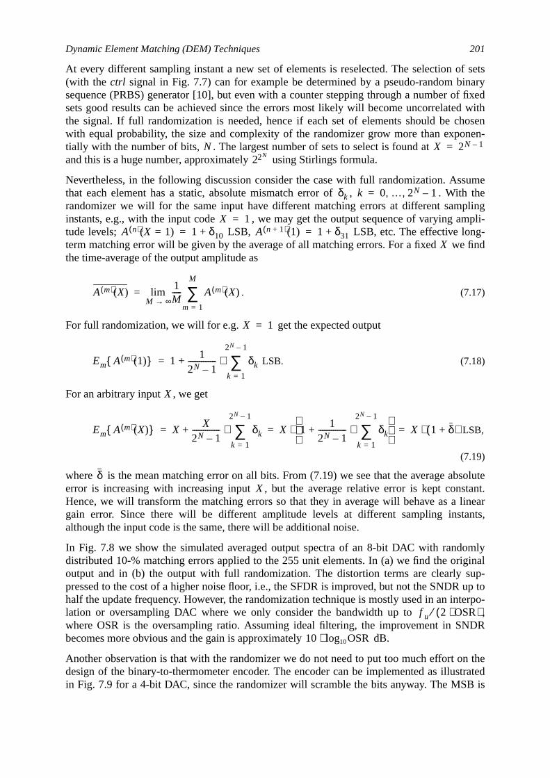
Dynamic Element Matching (DEM) Techniques 201
f setsnaryf fixedd withhosennen-
umetheling
mpli--find
solutetant.
linearnts,
omlyginalup-up to
terpo-,
DR
n thestratedB is
At every different sampling instant a new set of elements is reselected. The selection o(with the ctrl signal in Fig. 7.7) can for example be determined by a pseudo-random bisequence (PRBS) generator [10], but even with a counter stepping through a number osets good results can be achieved since the errors most likely will become uncorrelatethe signal. If full randomization is needed, hence if each set of elements should be cwith equal probability, the size and complexity of the randomizer grow more than expotially with the number of bits, . The largest number of sets to select is found atand this is a huge number, approximately using Stirlings formula.
Nevertheless, in the following discussion consider the case with full randomization. Assthat each element has a static, absolute mismatch error of , . Withrandomizer we will for the same input have different matching errors at different sampinstants, e.g., with the input code , we may get the output sequence of varying atude levels; LSB, LSB, etc. The effective longterm matching error will be given by the average of all matching errors. For a fixed wethe time-average of the output amplitude as
. (7.17)
For full randomization, we will for e.g. get the expected output
LSB. (7.18)
For an arbitrary input , we get
LSB,
(7.19)
where is the mean matching error on all bits. From (7.19) we see that the average aberror is increasing with increasing input , but the average relative error is kept consHence, we will transform the matching errors so that they in average will behave as again error. Since there will be different amplitude levels at different sampling instaalthough the input code is the same, there will be additional noise.
In Fig. 7.8 we show the simulated averaged output spectra of an 8-bit DAC with randdistributed 10-% matching errors applied to the 255 unit elements. In (a) we find the orioutput and in (b) the output with full randomization. The distortion terms are clearly spressed to the cost of a higher noise floor, i.e., the SFDR is improved, but not the SNDRhalf the update frequency. However, the randomization technique is mostly used in an inlation or oversampling DAC where we only consider the bandwidth up towhere OSR is the oversampling ratio. Assuming ideal filtering, the improvement in SNbecomes more obvious and the gain is approximately dB.
Another observation is that with the randomizer we do not need to put too much effort odesign of the binary-to-thermometer encoder. The encoder can be implemented as illuin Fig. 7.9 for a 4-bit DAC, since the randomizer will scramble the bits anyway. The MS
N X 2N 1–=22N
δk k 0 … 2N 1–, ,=
X 1=A n( ) X 1=( ) 1 δ10+= A n 1+( ) 1( ) 1 δ31+=
X
A m( ) X( )1M----- A m( ) X( )
m 1=
M
∑M ∞→lim=
X 1=
Em A m( ) 1( ) 11
2N 1–--------------- δk
k 1=
2N 1–
∑⋅+=
X
Em A m( ) X( ) XX
2N 1–--------------- δk
k 1=
2N 1–
∑⋅+ X 11
2N 1–--------------- δk
k 1=
2N 1–
∑⋅+
⋅ X 1 δ+( )⋅= = =
δX
f u 2 OSR⋅( )⁄
10 OSRlog10⋅
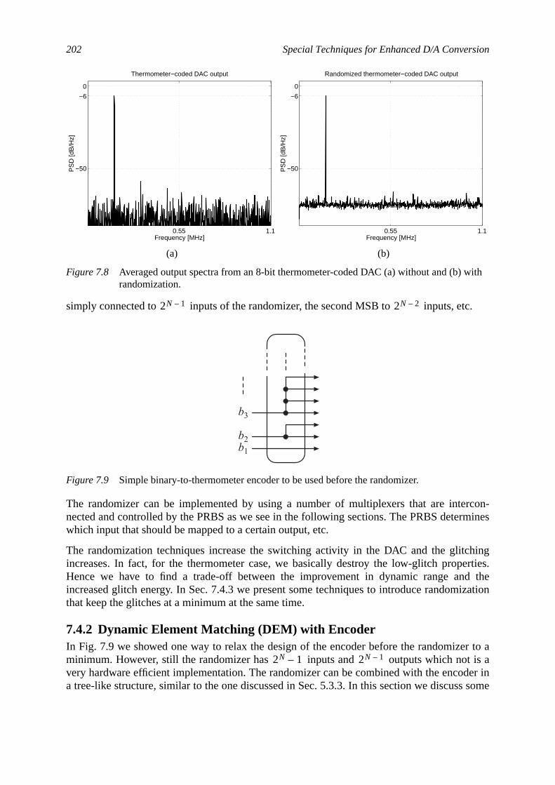
202 Special Techniques for Enhanced D/A Conversion
c.
rcon-mines
hingrties.
d theization
r to ais ader in
some
ith
simply connected to inputs of the randomizer, the second MSB to inputs, et
The randomizer can be implemented by using a number of multiplexers that are intenected and controlled by the PRBS as we see in the following sections. The PRBS deterwhich input that should be mapped to a certain output, etc.
The randomization techniques increase the switching activity in the DAC and the glitcincreases. In fact, for the thermometer case, we basically destroy the low-glitch propeHence we have to find a trade-off between the improvement in dynamic range anincreased glitch energy. In Sec. 7.4.3 we present some techniques to introduce randomthat keep the glitches at a minimum at the same time.
7.4.2 Dynamic Element Matching (DEM) with EncoderIn Fig. 7.9 we showed one way to relax the design of the encoder before the randomizeminimum. However, still the randomizer has inputs and outputs which notvery hardware efficient implementation. The randomizer can be combined with the encoa tree-like structure, similar to the one discussed in Sec. 5.3.3. In this section we discuss
(a) (b)
Figure 7.8 Averaged output spectra from an 8-bit thermometer-coded DAC (a) without and (b) wrandomization.
Figure 7.9 Simple binary-to-thermometer encoder to be used before the randomizer.
0.55 1.1
−50
−6
0
Frequency [MHz]
PS
D [d
B/H
z]Thermometer−coded DAC output
0.55 1.1
−50
−6
0
Frequency [MHz]
PS
D [d
B/H
z]
Randomized thermometer−coded DAC output
2N 1– 2N 2–
b1
b2
b3
2N 1– 2N 1–
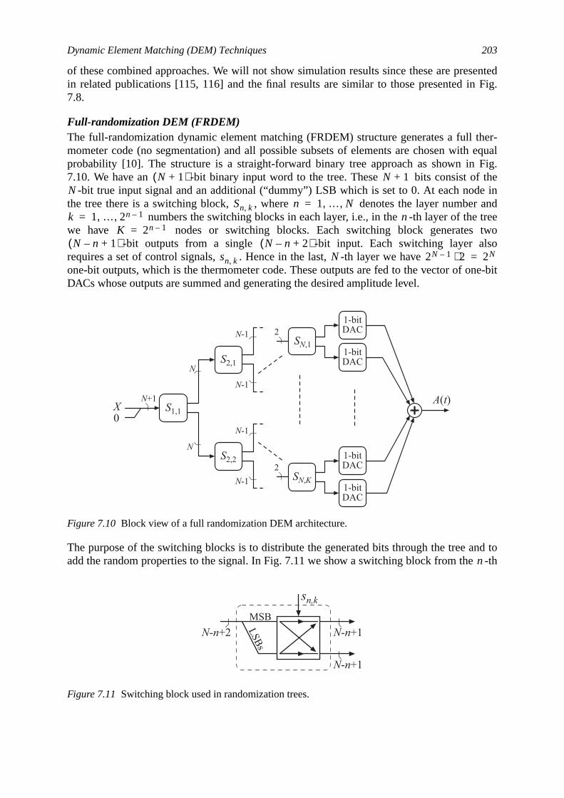
Dynamic Element Matching (DEM) Techniques 203
sentedFig.
ther-h equalFig.thein
andtreetwoo
ne-bit
nd to-th
of these combined approaches. We will not show simulation results since these are prein related publications [115, 116] and the final results are similar to those presented in7.8.
Full-randomization DEM (FRDEM)The full-randomization dynamic element matching (FRDEM) structure generates a fullmometer code (no segmentation) and all possible subsets of elements are chosen witprobability [10]. The structure is a straight-forward binary tree approach as shown in7.10. We have an -bit binary input word to the tree. These bits consist of
-bit true input signal and an additional (“dummy”) LSB which is set to 0. At each nodethe tree there is a switching block, , where denotes the layer number
numbers the switching blocks in each layer, i.e., in the -th layer of thewe have nodes or switching blocks. Each switching block generates
-bit outputs from a single -bit input. Each switching layer alsrequires a set of control signals, . Hence in the last, -th layer we haveone-bit outputs, which is the thermometer code. These outputs are fed to the vector of oDACs whose outputs are summed and generating the desired amplitude level.
The purpose of the switching blocks is to distribute the generated bits through the tree aadd the random properties to the signal. In Fig. 7.11 we show a switching block from the
Figure 7.10 Block view of a full randomization DEM architecture.
Figure 7.11 Switching block used in randomization trees.
N 1+( ) N 1+N
Sn k, n 1 … N, ,=k 1 … 2n 1–, ,= n
K 2n 1–=N n– 1+( ) N n– 2+( )
sn k, N 2N 1– 2⋅ 2N=
0X
N+1S1,1
NS2,2
S2,1N
N-1
N-1
N-1
N-1 SN,K
1-bitDAC
1-bitDAC
2
SN,1
1-bitDAC
1-bitDAC
2
A(t)
n
sn,k
N-n+2 N-n+1
N-n+1
MSB
LSBs
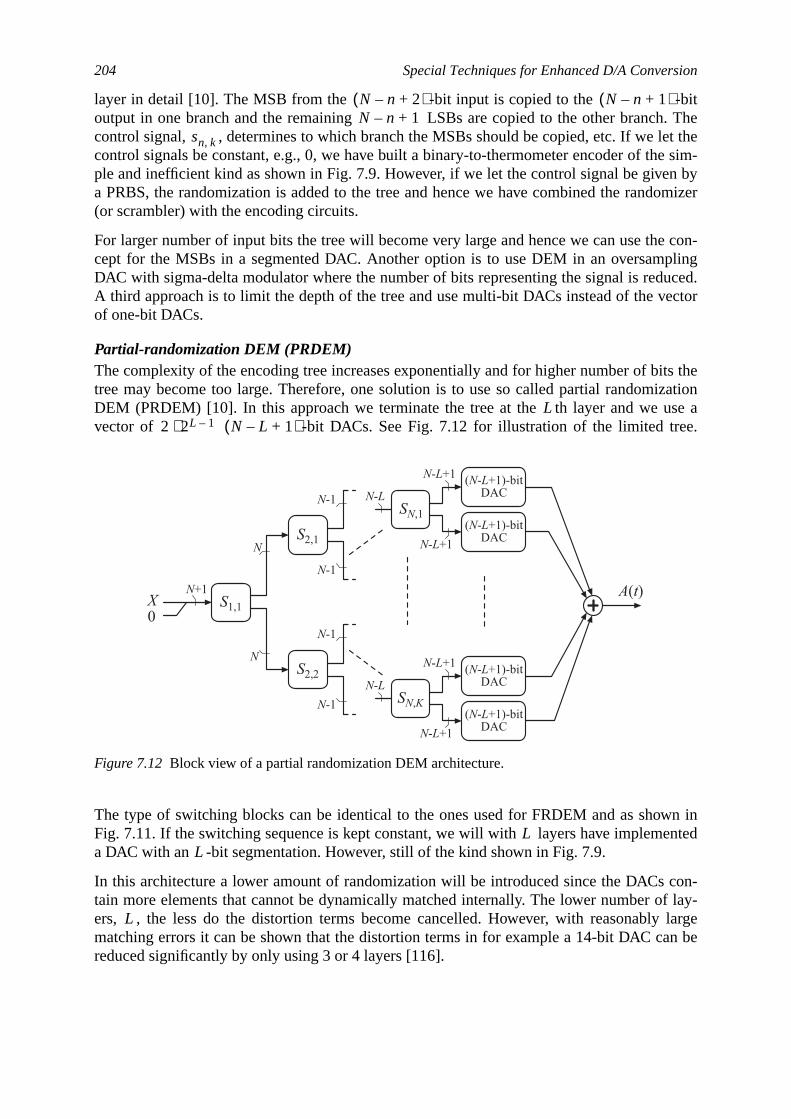
204 Special Techniques for Enhanced D/A Conversion
it. Thet the
e sim-n byomizer
con-ling
uced.ctor
ts thezationse ae.
wn innted
con-f lay-largen be
layer in detail [10]. The MSB from the -bit input is copied to the -boutput in one branch and the remaining LSBs are copied to the other branchcontrol signal, , determines to which branch the MSBs should be copied, etc. If we lecontrol signals be constant, e.g., 0, we have built a binary-to-thermometer encoder of thple and inefficient kind as shown in Fig. 7.9. However, if we let the control signal be givea PRBS, the randomization is added to the tree and hence we have combined the rand(or scrambler) with the encoding circuits.
For larger number of input bits the tree will become very large and hence we can use thecept for the MSBs in a segmented DAC. Another option is to use DEM in an oversampDAC with sigma-delta modulator where the number of bits representing the signal is redA third approach is to limit the depth of the tree and use multi-bit DACs instead of the veof one-bit DACs.
Partial-randomization DEM (PRDEM)The complexity of the encoding tree increases exponentially and for higher number of bitree may become too large. Therefore, one solution is to use so called partial randomiDEM (PRDEM) [10]. In this approach we terminate the tree at the th layer and we uvector of -bit DACs. See Fig. 7.12 for illustration of the limited tre
The type of switching blocks can be identical to the ones used for FRDEM and as shoFig. 7.11. If the switching sequence is kept constant, we will with layers have implemea DAC with an -bit segmentation. However, still of the kind shown in Fig. 7.9.
In this architecture a lower amount of randomization will be introduced since the DACstain more elements that cannot be dynamically matched internally. The lower number oers, , the less do the distortion terms become cancelled. However, with reasonablymatching errors it can be shown that the distortion terms in for example a 14-bit DAC careduced significantly by only using 3 or 4 layers [116].
Figure 7.12 Block view of a partial randomization DEM architecture.
N n– 2+( ) N n– 1+( )N n– 1+
sn k,
L2 2L 1–⋅ N L– 1+( )
0X
N+1S1,1
NS2,2
S2,1N
N-1
N-1
N-1
N-1 SN,K
SN,1
A(t)
(N-L+1)-bitDAC
(N-L+1)-bitDAC
(N-L+1)-bitDAC
(N-L+1)-bitDAC
N-L+1
N-L+1
N-L+1
N-L+1
N-L
N-L
LL
L
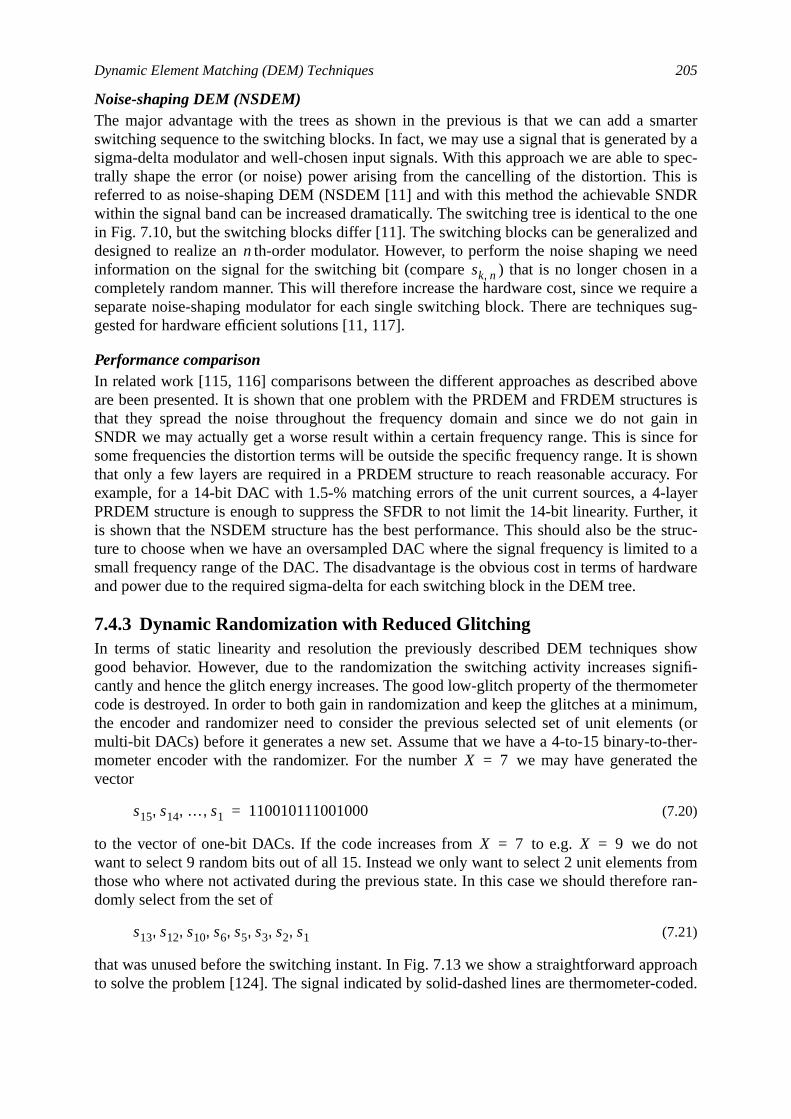
Dynamic Element Matching (DEM) Techniques 205
marterd by aspec-is isNDRe oneandneed
in auire as sug-
aboveres isain ine forhowny. Forayerer, itstruc-d to adware
howgnifi-metermum,nts (or-ther-d the
notfrom
re ran-
roachoded.
Noise-shaping DEM (NSDEM)The major advantage with the trees as shown in the previous is that we can add a sswitching sequence to the switching blocks. In fact, we may use a signal that is generatesigma-delta modulator and well-chosen input signals. With this approach we are able totrally shape the error (or noise) power arising from the cancelling of the distortion. Threferred to as noise-shaping DEM (NSDEM [11] and with this method the achievable Swithin the signal band can be increased dramatically. The switching tree is identical to thin Fig. 7.10, but the switching blocks differ [11]. The switching blocks can be generalizeddesigned to realize an th-order modulator. However, to perform the noise shaping weinformation on the signal for the switching bit (compare ) that is no longer chosencompletely random manner. This will therefore increase the hardware cost, since we reqseparate noise-shaping modulator for each single switching block. There are techniquegested for hardware efficient solutions [11, 117].
Performance comparisonIn related work [115, 116] comparisons between the different approaches as describedare been presented. It is shown that one problem with the PRDEM and FRDEM structuthat they spread the noise throughout the frequency domain and since we do not gSNDR we may actually get a worse result within a certain frequency range. This is sincsome frequencies the distortion terms will be outside the specific frequency range. It is sthat only a few layers are required in a PRDEM structure to reach reasonable accuracexample, for a 14-bit DAC with 1.5-% matching errors of the unit current sources, a 4-lPRDEM structure is enough to suppress the SFDR to not limit the 14-bit linearity. Furthis shown that the NSDEM structure has the best performance. This should also be theture to choose when we have an oversampled DAC where the signal frequency is limitesmall frequency range of the DAC. The disadvantage is the obvious cost in terms of harand power due to the required sigma-delta for each switching block in the DEM tree.
7.4.3 Dynamic Randomization with Reduced GlitchingIn terms of static linearity and resolution the previously described DEM techniques sgood behavior. However, due to the randomization the switching activity increases sicantly and hence the glitch energy increases. The good low-glitch property of the thermocode is destroyed. In order to both gain in randomization and keep the glitches at a minithe encoder and randomizer need to consider the previous selected set of unit elememulti-bit DACs) before it generates a new set. Assume that we have a 4-to-15 binary-tomometer encoder with the randomizer. For the number we may have generatevector
(7.20)
to the vector of one-bit DACs. If the code increases from to e.g. we dowant to select 9 random bits out of all 15. Instead we only want to select 2 unit elementsthose who where not activated during the previous state. In this case we should therefodomly select from the set of
(7.21)
that was unused before the switching instant. In Fig. 7.13 we show a straightforward appto solve the problem [124]. The signal indicated by solid-dashed lines are thermometer-c
nsk n,
X 7=
s15 s14 … s1, , , 110010111001000=
X 7= X 9=
s13 s12 s10 s6 s5 s3 s2 s1, , , , , , ,
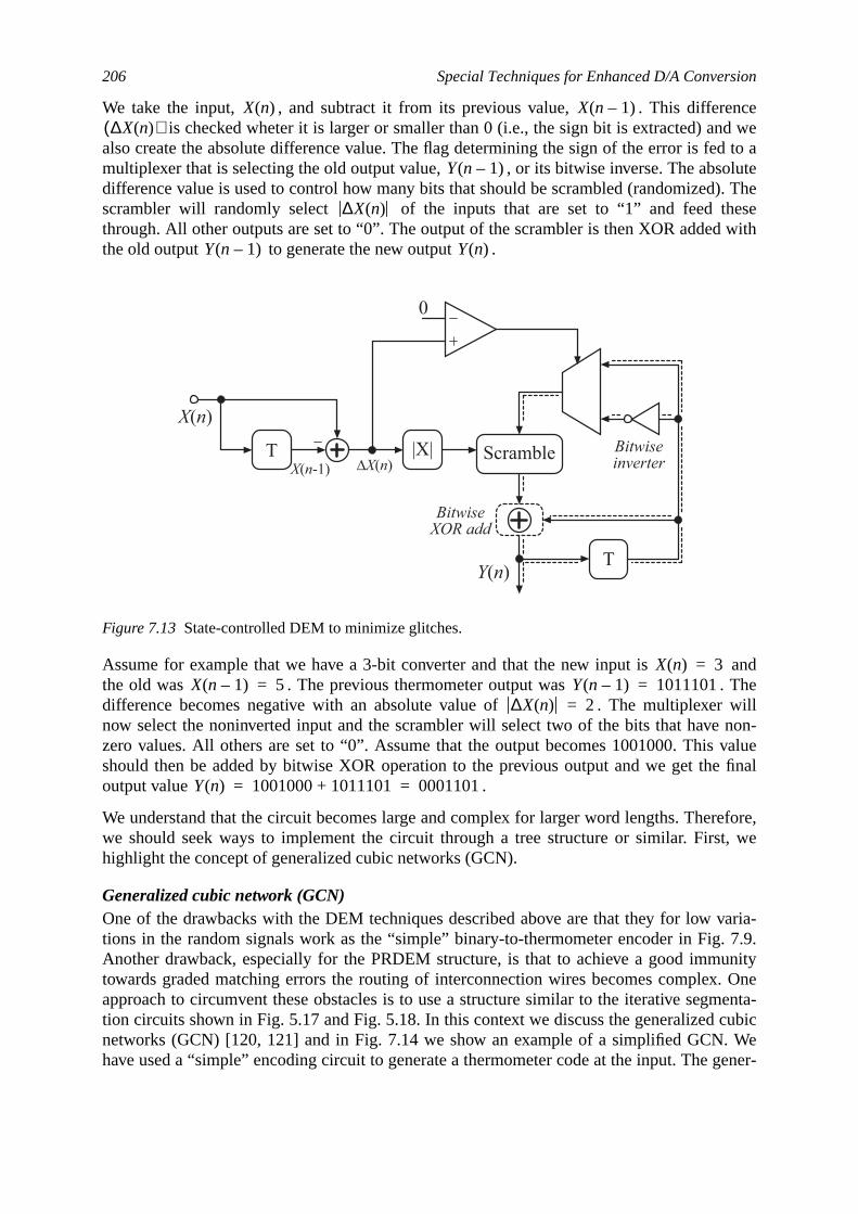
206 Special Techniques for Enhanced D/A Conversion
nced wed to alute
). Theesewith
andhewillnon-valuefinal
efore,t, we
varia-7.9.
unity. Onementa-cubicWe
gener-
We take the input, , and subtract it from its previous value, . This differeis checked wheter it is larger or smaller than 0 (i.e., the sign bit is extracted) an
also create the absolute difference value. The flag determining the sign of the error is femultiplexer that is selecting the old output value, , or its bitwise inverse. The absodifference value is used to control how many bits that should be scrambled (randomizedscrambler will randomly select of the inputs that are set to “1” and feed ththrough. All other outputs are set to “0”. The output of the scrambler is then XOR addedthe old output to generate the new output .
Assume for example that we have a 3-bit converter and that the new input isthe old was . The previous thermometer output was . Tdifference becomes negative with an absolute value of . The multiplexernow select the noninverted input and the scrambler will select two of the bits that havezero values. All others are set to “0”. Assume that the output becomes 1001000. Thisshould then be added by bitwise XOR operation to the previous output and we get theoutput value .
We understand that the circuit becomes large and complex for larger word lengths. Therwe should seek ways to implement the circuit through a tree structure or similar. Firshighlight the concept of generalized cubic networks (GCN).
Generalized cubic network (GCN)One of the drawbacks with the DEM techniques described above are that they for lowtions in the random signals work as the “simple” binary-to-thermometer encoder in Fig.Another drawback, especially for the PRDEM structure, is that to achieve a good immtowards graded matching errors the routing of interconnection wires becomes complexapproach to circumvent these obstacles is to use a structure similar to the iterative segtion circuits shown in Fig. 5.17 and Fig. 5.18. In this context we discuss the generalizednetworks (GCN) [120, 121] and in Fig. 7.14 we show an example of a simplified GCN.have used a “simple” encoding circuit to generate a thermometer code at the input. The
Figure 7.13 State-controlled DEM to minimize glitches.
X n( ) X n 1–( )∆X n( )( )
Y n 1–( )
∆X n( )
Y n 1–( ) Y n( )
T
0
X(n)
X(n-1) DX(n)
T
BitwiseXOR add
|X| Scramble
Y(n)
Bitwiseinverter
X n( ) 3=X n 1–( ) 5= Y n 1–( ) 1011101=
∆X n( ) 2=
Y n( ) 1001000 1011101+ 0001101= =
Dynamic Element Matching (DEM) Techniques 207
smis-s are
.e lethe cir-ave a
s sec-e treeyerimi-r the
workillus-
tatesbjectivechingn in
plied,f the, tothe
nted
alized version allows a true thermometer coded input. Further we use a number of transion gates (or the and-or pairs) in 2-to-2 muxes, , where the states of the muxedetermined by a number of control signals, , where andWe can choose to apply equal control signal for each layer as well, i.e., . If wthe control signals be random (or pseudo-random), we get a random data path through tcuit. Since the bits will interleave through the tree more or less by them selves, we will hgood immunity towards graded errors as well.
Dependent on implementation, we need not, unlike the DEM structures from the previoutions, to feed all bits through the entire tree (as in Sec. 5.3.3). We can also terminate th“from the other direction” than in the PRDEM. Hence, we feed forward the LSBs to la
and distribute them together with the MSBs to the muxes in an interdigitized way slar to that of Fig. 7.9. In terms of partial randomization we can choose to add the GCN foMSBs only.
Hardware Efficient dynamic randomization with reduced glitchingA hardware efficient approach to solve the problem with glitches is presented in related[123, 124]. The purpose with this approach is to combine the tree-structured encoder (astrated in Fig. 7.14), with the randomization, and glitch reduction. Instead of saving the sof selected sets and comparing the consecutive codes as in the approach above, the ois now to save the data path through the tree. For this purpose, we modify the switblocks as is illustrated in Fig. 7.15 and each block follows a decision table as showTable 7.1. Once again, we find in the figure the and-or pair and if no randomization is apthe outputs and are selected as and , respectively. The operation oblock is simple; if the bit has changed its value, we use a random switch signal,choose one of the outputs. In related work [122, 123, 124] simulation results show
Figure 7.14 Segmentation and scrambling 3-to-7 binary-to-thermometer encoding circuit implemeby a GCN.
Sn k,sn k, n 1 … N, ,= k 1 … 2N 1–, ,=
cn k, cn=
0
b0
b1
t2
t1
t3
t4
s1,1
s1,2
s1,3
s1,4
s2,1
s2,2
s2,3
s2,4
s3,1
s3,2
s3,3
s3,4
b2
t6
t5
t7
t8
KK 1+
xn k, yn k, an k, bn k,sn k,
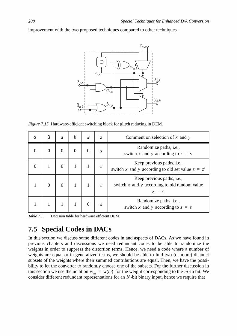
208 Special Techniques for Enhanced D/A Conversion
nd inize theber ofjunctpossi-
ion inWe
that
improvement with the two proposed techniques compared to other techniques.
7.5 Special Codes in DACsIn this section we discuss some different codes in and aspects of DACs. As we have fouprevious chapters and discussions we need redundant codes to be able to randomweights in order to suppress the distortion terms. Hence, we need a code where a numweights are equal or in generalized terms, we should be able to find two (or more) dissubsets of the weights where their summed contributions are equal. Then, we have thebility to let the converter to randomly choose one of the subsets. For the further discussthis section we use the notation for the weight corresponding to the -th bit.consider different redundant representations for an -bit binary input, hence we require
Figure 7.15 Hardware-efficient switching block for glitch reducing in DEM.
Comment on selection of and
0 0 0 0 0Randomize paths, i.e.,
switch and according to
0 1 0 1 1Keep previous paths, i.e.,
switch and according to old set value
1 0 0 1 1
Keep previous paths, i.e.,switch and according to old random value
1 1 1 1 0Randomize paths, i.e.,
switch and according to
Table 7.1. Decision table for hardware efficient DEM.
sn,k
D
an,k
bn,k
an,k
bn,k
xn,k
yn,k
wn,kzn,k
α β a b w z x y
sx y z s=
z'x y z z'=
z' x y
z z'=
sx y z s=
wm w m( )= mN

Special Codes in DACs 209
fortherbuttwoher-utions.men-ep the
hings, thend the
some-are toiza-
forces to
at isdencys reset
rsionerentmeterer ofe
a full-
. (7.22)
One code that fulfils this relation with equality is the thermometer code, where. We have a high degree of flexibility when chosing the subsets. Ano
solution is to segment the input, hence, we have for the LSBs,for the MSBs. Further, we can point out the rather naive case of using
parallel DACs where the two inputs are chopped, etc. A drawback with using the full tmometer-code representation is that the digital hardware becomes large for higher resolTo keep the amount of hardware low, we prefer segmentation instead. With shrinking disions though, this cost measure becomes of minor interest. Still, however, we want to kepower dissipation low.
In terms of glitching, the thermometer code is optimal since the number of bits switcbetween two consecutive samples as the input is ramped is minimum. In those termbinary code shows the worst behavior. In between these two extremes, we once again fisegmented code.
In Sec. 7.5.1 we present the studies on linear-coded DACs. We investigate a code that iswhere in-between the full thermometer code and the binary code. The design issuesminimize glitches, to allow a fairly easy layout technique, and redundant code for randomtion techniques.
In Sec. 7.5.2 we discuss the commonly known signed-digit code which is suitable inexample current-steering DACs where we can use both NMOS and PMOS current sourgenerate positive and negative output currents.
In an implementation of the current switches it is likely to get a switching time instant thdependent on the previous value applied to the switch. This switch memory, or depencan be reduced by using a return-to-zero code (R2Z) where the state of the switches ieach update period. This is further discussed in Sec. 7.5.3.
7.5.1 Linear-Coded DACsIn Chapter 2 we find a summary of different codes that are/can be used for D/A conveand in Chapter 3 we found some different techniques to realize the converters for diffcodes. In our work, we have investigated some codes that are between the full thermocode and the binary code [32, 33, 34, 35]. The full thermometer code shows a high ordredundancy whereas the binary code is not redundant at all. For the linear code, we hav
for . (7.23)
must be large enough so that the inequality of (7.22) is met (to be able to representscale signal). We get
. (7.24)
This gives the approximate value on
wmm 1=
M
∑ 2N 1–≥
w m( ) 1=m 1 … 2N 1–, ,=
w m( ) 2m 1–= Kw m( ) 2K= N K–
wm w m( ) m= = m 1 … M, ,=
M
w m( )m 1=
M
∑ mm 1=
M
∑ M M 1+( )⋅2
----------------------------- 2N 1–≥= =
M
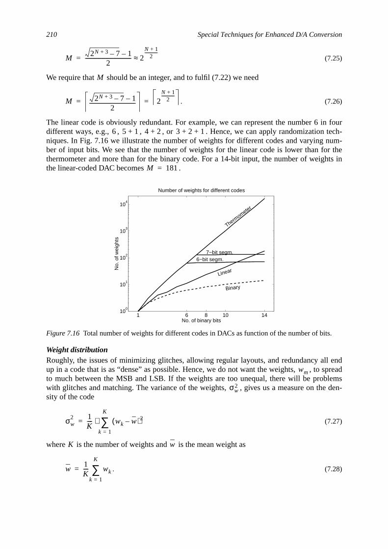
210 Special Techniques for Enhanced D/A Conversion
n fourch-um-r thehts in
l endpreadlems
den-
.
(7.25)
We require that should be an integer, and to fulfil (7.22) we need
. (7.26)
The linear code is obviously redundant. For example, we can represent the number 6 idifferent ways, e.g., , , , or . Hence, we can apply randomization teniques. In Fig. 7.16 we illustrate the number of weights for different codes and varying nber of input bits. We see that the number of weights for the linear code is lower than fothermometer and more than for the binary code. For a 14-bit input, the number of weigthe linear-coded DAC becomes .
Weight distributionRoughly, the issues of minimizing glitches, allowing regular layouts, and redundancy alup in a code that is as “dense” as possible. Hence, we do not want the weights, , to sto much between the MSB and LSB. If the weights are too unequal, there will be probwith glitches and matching. The variance of the weights, , gives us a measure on thesity of the code
(7.27)
where is the number of weights and is the mean weight as
. (7.28)
Figure 7.16 Total number of weights for different codes in DACs as function of the number of bits
M2N 3+ 7– 1–
2----------------------------------- 2
N 1+2
-------------≈=
M
M 2N 3+ 7– 1–2
----------------------------------- 2N 1+
2-------------
= =
6 5 1+ 4 2+ 3 2 1+ +
M 181=
1 6 8 10 1410
0
101
102
103
104
Thermometer
Linear
Binary
7−bit segm.6−bit segm.
Number of weights for different codes
No.
of w
eigh
ts
No. of binary bits
wm
σw2
σw2 1
K---- wk w–( )2
k 1=
K
∑⋅=
K w
w1K---- wk
k 1=
K
∑=

Special Codes in DACs 211
For the
r (orseg-
et the
iation, fored to
rter. Weget 14
For the binary code, we get for example
(7.29)
and
. (7.30)
For the thermometer code, we get
and . (7.31)
Since all weights are equally large, there is no spread and hence the variance is zero.linear code, we get
(7.32)
and
. (7.33)
Comparing (7.33) with (7.30) tells us that the linear code for all number of bits has a loweequal to for ) standard deviation. However, we can compare the result with themented converter in stead. For thise case, we will for a thermometer coded MSBs gaverage weight
(7.34)
and the variance
. (7.35)
For example, for a 14-bit converter, we would for the binary converter get a standard devof 2326 and for the linear converter only 52. However, for a 6-bit segmentation we get 73a 7-bit segmentation about 25. Hence, heuristically, for the 14-bit binary converter, we nesegment at least 6 or 7 bits to achieve the same performance as the linear-coded convemay also consider the number of weights in the different cases. For the binary case, we
wB1N---- 2m 1–
m 1=
N
∑ 2N 1–N
--------------- 2N
N------≈= =
σwB2 1
N---- 2m 1– 2N
N------–
2
m 1=
N
∑ 22N N 3–3N2-------------⋅= =
wT1
2N 1–--------------- 1
m 1=
2N 1–
∑ 1= = σwT2
0=
wL1M----- m
m 1=
M
∑ M M 1+( )⋅2M
----------------------------- M 1+2
-------------- M2----- 2
N 1–2
-------------≈ ≈ ≈= =
σwL2 1
M----- m
M 1+2
--------------– 2
m 1=
M
∑ M 1+( ) M 1 2⁄+( )⋅3
-------------------------------------------------- M 1+( )2
4----------------------–
M2
12------- 2N 1–
3-------------≈ ≈= =
N 1 2,=K
wS1
N K– 2K 1–+------------------------------------ 2m 1–
m 1=
N K–
∑ 2N K–
m 1=
2K 1–
∑+ 2N 1–
N K– 2K 1–+------------------------------------= =
σwS2 1
N K– 2K 1–+------------------------------------ 2m 1– wS–( )2
m 1=
N K–
∑ 2N K– wS–( )2
m 1=
2K 1–
∑+
≈=
22N K– N K– 2–N K– 2K+( )2
-----------------------------------⋅≈
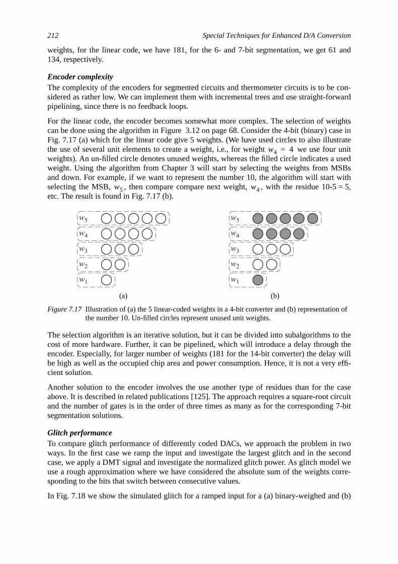
212 Special Techniques for Enhanced D/A Conversion
1 and
con-rward
eightsase intrateunitusedBswith= 5,
thethewill
y effi-
casecircuitg 7-bit
twoecondl wecorre-
d (b)
n of
weights, for the linear code, we have 181, for the 6- and 7-bit segmentation, we get 6134, respectively.
Encoder complexityThe complexity of the encoders for segmented circuits and thermometer circuits is to besidered as rather low. We can implement them with incremental trees and use straight-fopipelining, since there is no feedback loops.
For the linear code, the encoder becomes somewhat more complex. The selection of wcan be done using the algorithm in Figure 3.12 on page 68. Consider the 4-bit (binary) cFig. 7.17 (a) which for the linear code give 5 weights. (We have used circles to also illusthe use of several unit elements to create a weight, i.e., for weight we use fourweights). An un-filled circle denotes unused weights, whereas the filled circle indicates aweight. Using the algorithm from Chapter 3 will start by selecting the weights from MSand down. For example, if we want to represent the number 10, the algorithm will startselecting the MSB, , then compare compare next weight, , with the residue 10-5etc. The result is found in Fig. 7.17 (b).
The selection algorithm is an iterative solution, but it can be divided into subalgorithms tocost of more hardware. Further, it can be pipelined, which will introduce a delay throughencoder. Especially, for larger number of weights (181 for the 14-bit converter) the delaybe high as well as the occupied chip area and power consumption. Hence, it is not a vercient solution.
Another solution to the encoder involves the use another type of residues than for theabove. It is described in related publications [125]. The approach requires a square-rootand the number of gates is in the order of three times as many as for the correspondinsegmentation solutions.
Glitch performanceTo compare glitch performance of differently coded DACs, we approach the problem inways. In the first case we ramp the input and investigate the largest glitch and in the scase, we apply a DMT signal and investigate the normalized glitch power. As glitch modeuse a rough approximation where we have considered the absolute sum of the weightssponding to the bits that switch between consecutive values.
In Fig. 7.18 we show the simulated glitch for a ramped input for a (a) binary-weighed an
(a) (b)
Figure 7.17 Illustration of (a) the 5 linear-coded weights in a 4-bit converter and (b) representatiothe number 10. Un-filled circles represent unused unit weights.
w4 4=
w5 w4
w2
w1
w3
w4
w5
w2
w1
w3
w4
w5
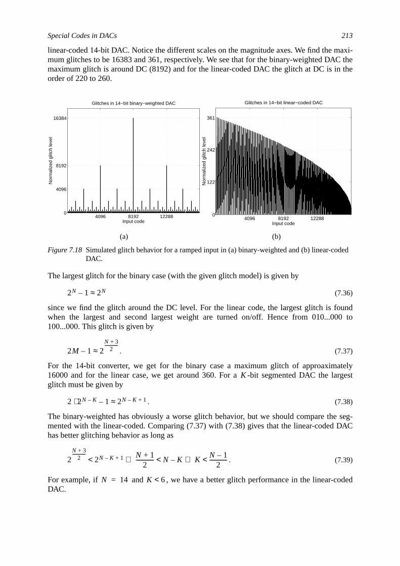
Special Codes in DACs 213
axi-C thethe
und00 to
atelyrgest
seg-DAC
ded
ded
linear-coded 14-bit DAC. Notice the different scales on the magnitude axes. We find the mmum glitches to be 16383 and 361, respectively. We see that for the binary-weighted DAmaximum glitch is around DC (8192) and for the linear-coded DAC the glitch at DC is inorder of 220 to 260.
The largest glitch for the binary case (with the given glitch model) is given by
(7.36)
since we find the glitch around the DC level. For the linear code, the largest glitch is fowhen the largest and second largest weight are turned on/off. Hence from 010...0100...000. This glitch is given by
. (7.37)
For the 14-bit converter, we get for the binary case a maximum glitch of approaxim16000 and for the linear case, we get around 360. For a -bit segmented DAC the laglitch must be given by
. (7.38)
The binary-weighted has obviously a worse glitch behavior, but we should compare themented with the linear-coded. Comparing (7.37) with (7.38) gives that the linear-codedhas better glitching behavior as long as
. (7.39)
For example, if and , we have a better glitch performance in the linear-coDAC.
(a) (b)
Figure 7.18 Simulated glitch behavior for a ramped input in (a) binary-weighted and (b) linear-coDAC.
4096 8192 122880
4096
8192
16384
Glitches in 14−bit binary−weighted DAC
Input code
Nor
mal
ized
glit
ch le
vel
4096 8192 122880
122
242
361
Glitches in 14−bit linear−coded DAC
Input code
Nor
mal
ized
glit
ch le
vel
2N 1– 2N≈
2M 1– 2N 3+
2-------------
≈
K
2 2N K–⋅ 1– 2N K– 1+≈
2N 3+
2-------------
2N K– 1+< N 1+2
------------- N K–< KN 1–
2-------------<⇒ ⇒
N 14= K 6<
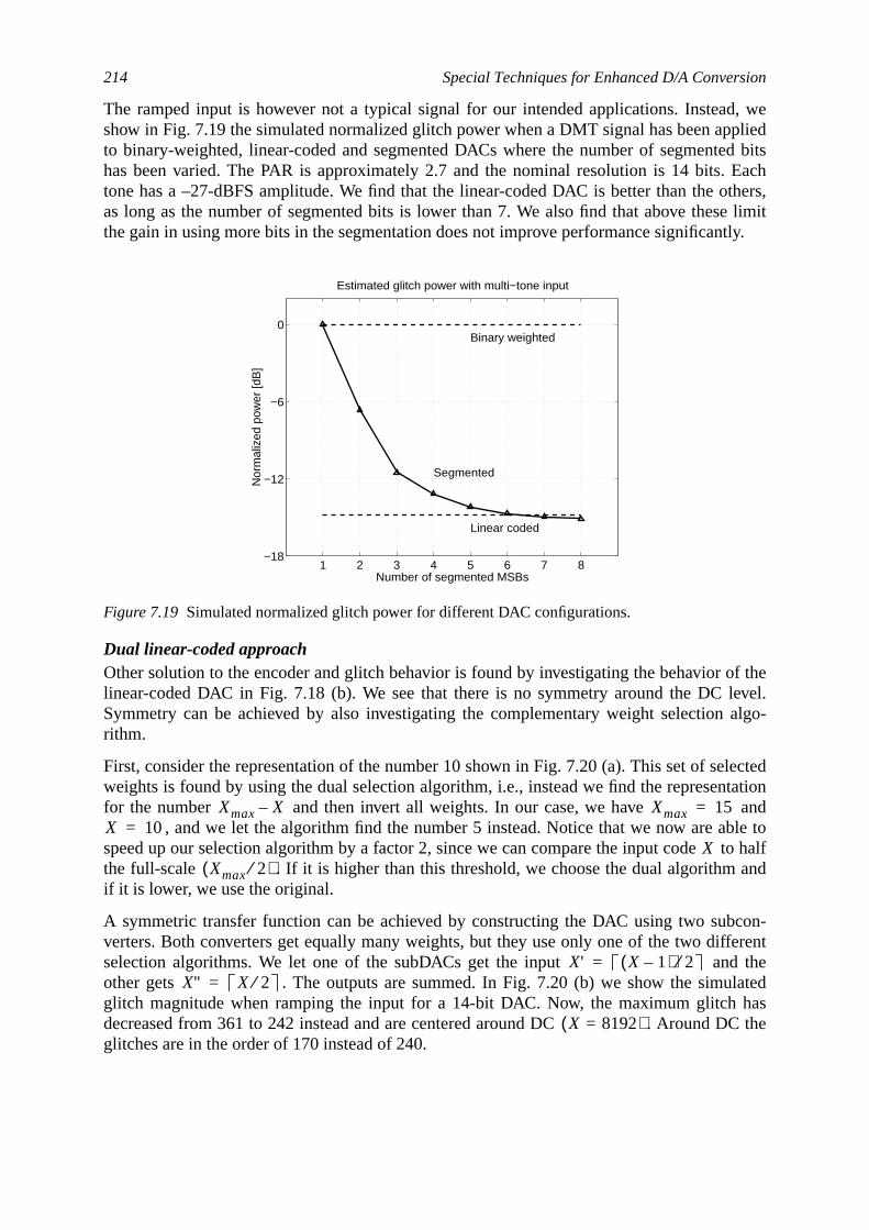
214 Special Techniques for Enhanced D/A Conversion
, wepliedd bitsEachthers,e limittly.
f theevel.algo-
lectedtationandle toto halfand
con-erentthe
latedhasC the
The ramped input is however not a typical signal for our intended applications. Insteadshow in Fig. 7.19 the simulated normalized glitch power when a DMT signal has been apto binary-weighted, linear-coded and segmented DACs where the number of segmentehas been varied. The PAR is approximately 2.7 and the nominal resolution is 14 bits.tone has a –27-dBFS amplitude. We find that the linear-coded DAC is better than the oas long as the number of segmented bits is lower than 7. We also find that above thesthe gain in using more bits in the segmentation does not improve performance significan
Dual linear-coded approachOther solution to the encoder and glitch behavior is found by investigating the behavior olinear-coded DAC in Fig. 7.18 (b). We see that there is no symmetry around the DC lSymmetry can be achieved by also investigating the complementary weight selectionrithm.
First, consider the representation of the number 10 shown in Fig. 7.20 (a). This set of seweights is found by using the dual selection algorithm, i.e., instead we find the represenfor the number and then invert all weights. In our case, we have
, and we let the algorithm find the number 5 instead. Notice that we now are abspeed up our selection algorithm by a factor 2, since we can compare the input codethe full-scale . If it is higher than this threshold, we choose the dual algorithmif it is lower, we use the original.
A symmetric transfer function can be achieved by constructing the DAC using two subverters. Both converters get equally many weights, but they use only one of the two diffselection algorithms. We let one of the subDACs get the input andother gets . The outputs are summed. In Fig. 7.20 (b) we show the simuglitch magnitude when ramping the input for a 14-bit DAC. Now, the maximum glitchdecreased from 361 to 242 instead and are centered around DC . Around Dglitches are in the order of 170 instead of 240.
Figure 7.19 Simulated normalized glitch power for different DAC configurations.
1 2 3 4 5 6 7 8−18
−12
−6
0Binary weighted
Linear coded
Segmented
Estimated glitch power with multi−tone input
Number of segmented MSBs
Nor
mal
ized
pow
er [d
B]
Xmax X– Xmax 15=X 10=
XXmax 2⁄( )
X' X 1–( ) 2⁄=X'' X 2⁄=
X 8192=( )
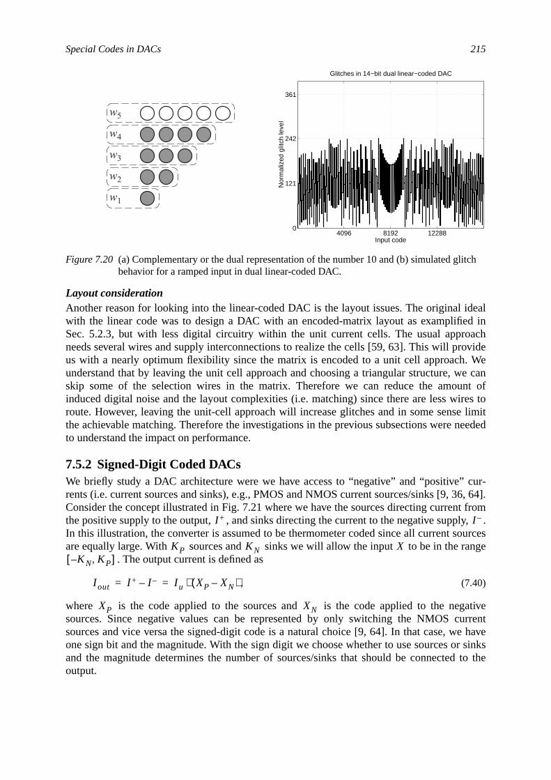
Special Codes in DACs 215
ideald inach
ovideWee cannt ofres tolimiteeded
cur-6, 64].t fromy, .ourcesnge
gativeurrente haver sinks
to the
litch
Layout considerationAnother reason for looking into the linear-coded DAC is the layout issues. The originalwith the linear code was to design a DAC with an encoded-matrix layout as examplifieSec. 5.2.3, but with less digital circuitry within the unit current cells. The usual approneeds several wires and supply interconnections to realize the cells [59, 63]. This will prus with a nearly optimum flexibility since the matrix is encoded to a unit cell approach.understand that by leaving the unit cell approach and choosing a triangular structure, wskip some of the selection wires in the matrix. Therefore we can reduce the amouinduced digital noise and the layout complexities (i.e. matching) since there are less wiroute. However, leaving the unit-cell approach will increase glitches and in some sensethe achievable matching. Therefore the investigations in the previous subsections were nto understand the impact on performance.
7.5.2 Signed-Digit Coded DACsWe briefly study a DAC architecture were we have access to “negative” and “positive”rents (i.e. current sources and sinks), e.g., PMOS and NMOS current sources/sinks [9, 3Consider the concept illustrated in Fig. 7.21 where we have the sources directing currenthe positive supply to the output, , and sinks directing the current to the negative supplIn this illustration, the converter is assumed to be thermometer coded since all current sare equally large. With sources and sinks we will allow the input to be in the ra
. The output current is defined as
, (7.40)
where is the code applied to the sources and is the code applied to the nesources. Since negative values can be represented by only switching the NMOS csources and vice versa the signed-digit code is a natural choice [9, 64]. In that case, wone sign bit and the magnitude. With the sign digit we choose whether to use sources oand the magnitude determines the number of sources/sinks that should be connectedoutput.
Figure 7.20 (a) Complementary or the dual representation of the number 10 and (b) simulated gbehavior for a ramped input in dual linear-coded DAC.
w2
w1
w3
w4
w5
4096 8192 122880
121
242
361
Glitches in 14−bit dual linear−coded DAC
Input code
Nor
mal
ized
glit
ch le
vel
I + I –
KP KN XKN– KP,[ ]
I out I + I –– I u XP XN–( )⋅= =
XP XN
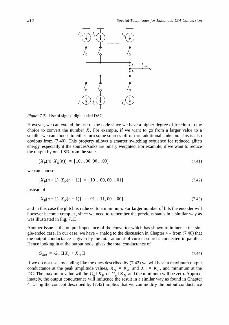
216 Special Techniques for Enhanced D/A Conversion
in theto as alsolitch
educe
r willway as
e sin-
rallel.
utputt thex-pter
tance
However, we can extend the use of the code since we have a higher degree of freedomchoice to convert the number . For example, if we want to go from a larger valuesmaller we can choose to either turn some sources off or turn additional sinks on. This iobvious from (7.40). This property allows a smarter switching sequence for reduced genergy, especially if the sources/sinks are binary weighted. For example, if we want to rthe output by one LSB from the state
(7.41)
we can choose
(7.42)
instead of
(7.43)
and in this case the glitch is reduced to a minimum. For larger number of bits the encodehowever become complex, since we need to remember the previous states in a similarwas illustrated in Fig. 7.13.
Another issue is the output impedance of the converter which has shown to influence thgle-ended case. In our case, we have – analog to the discussion in Chapter 4 – from (7.40) thatthe output conductance is given by the total amount of current sources connected in paHence looking in at the output node, gives the total conductance of
. (7.44)
If we do not use any coding like the ones described by (7.42) we will have a maximum oconductance at the peak amplitude values, and , and minimum aDC. The maximum value will be or and the minimum will be zero. Approimately, the output conductance will influence the result in a similar way as found in Cha4. Using the concept described by (7.42) implies that we can modify the output conduc
Figure 7.21 Use of signed-digit coded DAC.
Iu Iu Iu
Iu Iu Iu
IoutI+
I-
X
XP n( ) XN n( ),[ ] 10…00 00…00,[ ]=
XP n 1+( ) XN n 1+( ),[ ] 10…00 00…01,[ ]=
XP n 1+( ) XN n 1+( ),[ ] 01…11 00…00,[ ]=
Gout Gu XP XN+( )⋅=
XN KN= XP KP=Gu KP⋅ Gu KN⋅
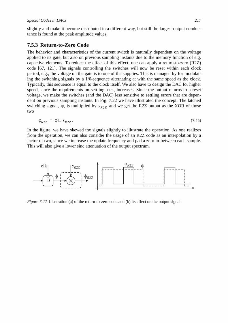
Special Codes in DACs 217
duc-
oltagef e.g.(R2Z)lockdulat-clock.
ighera resetepen-tchedose
lizesn by aample.
slightly and make it become distributed in a different way, but still the largest output contance is found at the peak amplitude values.
7.5.3 Return-to-Zero CodeThe behavior and characteristics of the current switch is naturally dependent on the vapplied to its gate, but also on previous sampling instants due to the memory function ocapactive elements. To reduce the effect of this effect, one can apply a return-to-zerocode [67, 121]. The signals controlling the switches will now be reset within each cperiod, e.g., the voltage on the gate is to one of the supplies. This is managed by for moing the switching signals by a 1/0-sequence alternating at with the same speed as theTypically, this sequence is equal to the clock itself. We also have to design the DAC for hspeed, since the requirements on settling, etc., increases. Since the output returns tovoltage, we make the switches (and the DAC) less sensitive to settling errors that are ddent on previous sampling instants. In Fig. 7.22 we have illustrated the concept. The laswitching signal, , is multiplied by and we get the R2Z output as the XOR of thtwo
. (7.45)
In the figure, we have skewed the signals slightly to illustrate the operation. As one reafrom the operation, we can also consider the usage of an R2Z code as an interpolatiofactor of two, since we increase the update frequency and pad a zero in-between each sThis will also give a lower sinc attenuation of the output spectrum.
Figure 7.22 Illustration (a) of the return-to-zero code and (b) its effect on the output signal.
φ sR2Z
φR2Z φ sR2Z⊕=
D
clk
f fR2Z
sR2ZfR2Z f

218 Special Techniques for Enhanced D/A Conversion
hapter3 wee cur-con-ms ofutedNDR
con-tio.ghoutPSD
ing aesentreso-whereownideal
nalbility.n be
8 Appendices8.1 IntroductionIn these appendices we present some of the derivations of the expressions in mainly C4. In App. 8.2 we present the derivation in the gain by using noise shaping. In App. 8.deal with the models that consider output conductance of the unit current sources in thrent-steering DAC. We find formulas on the SNDR and SFDR as functions of the outputductance for single-ended and differential outputs. App. 8.4 discusses how the waveforthe more significant bits for a sinusoid input have their Fourier components distribthroughout the frequency domain. This is used to find the expression on the SFDR and Sas function of the matching error.
8.2 Resolution Improvement Through Noise ShapingWe find that we can gain in performance by increasing the update frequency in a D/Averter. In dB, this gain is in the order of where OSR is the oversampling raSome of the LSBs are thrown away and the increased truncation noise is spread throuthe frequency domain. If the frequency range is large enough to suppress the noisewithin the signal band to the desired level, we can reach a higher performance by uslower-bit DAC. The resulting signal is a version of pulse code modulation, hence we repra certain amplitude level by the average of several amplitude levels. To reach very highlution the OSR needs to be extremely high and instead we prefer to use noise shapingthe truncated signal (or the truncation error) is fed back in a filtering loop rather than “thraway”. This is done by a modulator and we assume that for an th order modulator thenoise transfer function (NTF) is given by
(8.1)
where also is the order of the filtering function. In reality, we would require additiozeros and poles that are not placed on the unity circle for higher-order modulators for staThe quantization noise power within the signal frequency band, from 0 to , cafound by investigating the magnitude function on the unity circly. We have
10 OSRlog10⋅
L
NTF z( ) 1 z 1––( )L=
L
π OSR⁄
219
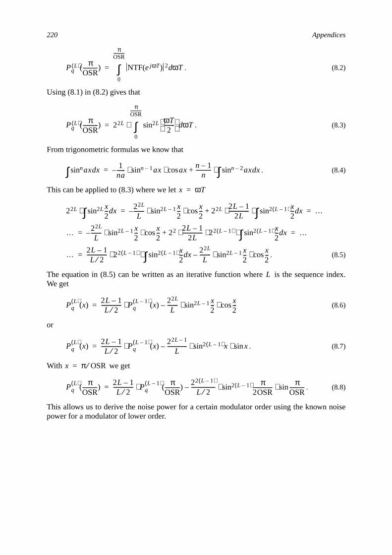
220 Appendices
ndex.
noise
. (8.2)
Using (8.1) in (8.2) gives that
. (8.3)
From trigonometric formulas we know that
. (8.4)
This can be applied to (8.3) where we let
. (8.5)
The equation in (8.5) can be written as an iterative function where is the sequence iWe get
(8.6)
or
. (8.7)
With we get
. (8.8)
This allows us to derive the noise power for a certain modulator order using the knownpower for a modulator of lower order.
PqL( ) π
OSR-----------( ) NTF ejωT( ) 2 ωTd
0
πOSR-----------
∫=
PqL( ) π
OSR-----------( ) 22L ωT
2--------
sin2L ωTd
0
πOSR-----------
∫⋅=
axsinn xd∫ 1na------– axsinn 1– axcos⋅ ⋅ n 1–
n------------ axsinn 2– xd∫⋅+=
x ωT=
22L x2---sin2L xd∫⋅ 22L
L--------– x
2---sin2L 1– x
2---cos⋅ ⋅ 22L 2L 1–
2L--------------- x
2---sin2 L 1–( ) xd∫⋅ ⋅+ …= =
… 22L
L--------– x
2---sin2L 1– x
2---cos⋅ ⋅ 22 2L 1–
2L--------------- 22 L 1–( ) x
2---sin2 L 1–( ) xd∫⋅ ⋅ ⋅+ …= =
… 2L 1–L 2⁄
--------------- 22 L 1–( ) x2---sin2 L 1–( ) xd∫⋅ ⋅ 22L
L-------- x
2---sin2L 1– x
2---cos⋅ ⋅–=
L
PqL( )
x( )2L 1–L 2⁄
--------------- PqL 1–( )
x( )⋅ 22L
L-------- x
2---sin2L 1– x
2---cos⋅ ⋅–=
PqL( )
x( )2L 1–L 2⁄
--------------- PqL 1–( )
x( )⋅ 22L 1–
L--------------- xsin2 L 1–( ) xsin⋅ ⋅–=
x π OSR⁄=
PqL( ) π
OSR-----------( )
2L 1–L 2⁄
--------------- PqL 1–( ) π
OSR-----------( )⋅ 22 L 1–( )
L 2⁄------------------ π
2OSR---------------sin2 L 1–( ) π
OSR-----------sin⋅ ⋅–=
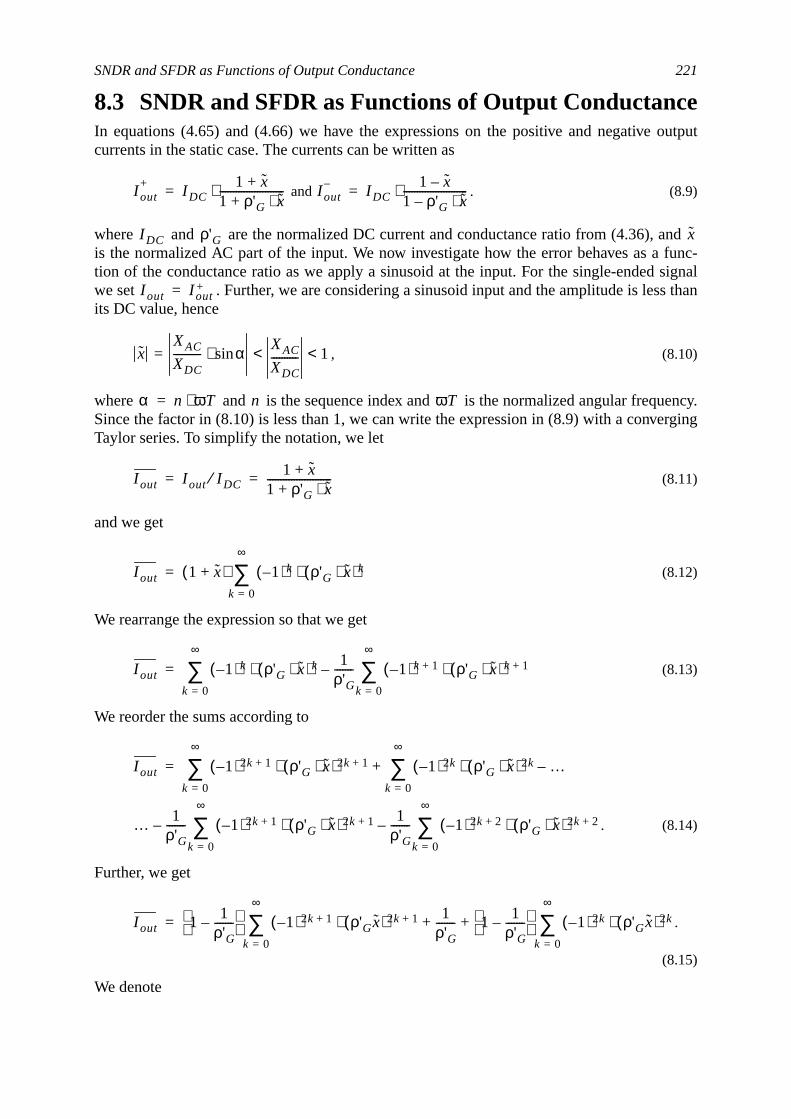
SNDR and SFDR as Functions of Output Conductance 221
output
ndfunc-signalthan
ency.rging
8.3 SNDR and SFDR as Functions of Output ConductanceIn equations (4.65) and (4.66) we have the expressions on the positive and negativecurrents in the static case. The currents can be written as
and . (8.9)
where and are the normalized DC current and conductance ratio from (4.36), ais the normalized AC part of the input. We now investigate how the error behaves as ation of the conductance ratio as we apply a sinusoid at the input. For the single-endedwe set . Further, we are considering a sinusoid input and the amplitude is lessits DC value, hence
, (8.10)
where and is the sequence index and is the normalized angular frequSince the factor in (8.10) is less than 1, we can write the expression in (8.9) with a conveTaylor series. To simplify the notation, we let
(8.11)
and we get
(8.12)
We rearrange the expression so that we get
(8.13)
We reorder the sums according to
. (8.14)
Further, we get
.
(8.15)
We denote
I out+
I DC1 x+
1 ρ'G x⋅+------------------------⋅= I out
–I DC
1 x–1 ρ'G x⋅–------------------------⋅=
I DC ρ'G x
I out I out+=
xXAC
XDC---------- αsin⋅ XAC
XDC----------<= 1<
α n ωT⋅= n ωT
I out I out I DC⁄ 1 x+1 ρ'G x⋅+------------------------= =
I out 1 x+( ) 1–( )k ρ'G x⋅( )k⋅k 0=
∞
∑=
I out 1–( )k ρ'G x⋅( )k⋅k 0=
∞
∑ 1ρ'G------- 1–( )k 1+ ρ'G x⋅( )k 1+⋅
k 0=
∞
∑–=
I out 1–( )2k 1+ ρ'G x⋅( )2k 1+⋅k 0=
∞
∑ 1–( )2k ρ'G x⋅( )2k⋅k 0=
∞
∑ …–+=
… 1ρ'G------- 1–( )2k 1+ ρ'G x⋅( )2k 1+⋅
k 0=
∞
∑ 1ρ'G------- 1–( )2k 2+ ρ'G x⋅( )2k 2+⋅
k 0=
∞
∑––
I out 1 1ρ'G-------–
1–( )2k 1+ ρ'Gx( )2k 1+⋅k 0=
∞
∑ 1ρ'G------- 1 1
ρ'G-------–
1–( )2k ρ'Gx( )2k⋅k 0=
∞
∑+ +=
222 Appendices
(8.19)
) andexam-u-
uble
formonic.
and . (8.16)
(8.15) is now rewritten as
(8.17)
We know that
(8.18)
and
. (8.19)
We now have a method to express the error by a number of harmonics. (8.18) andinserted in (8.17) gives
(8.20)
From this expression, we find identify the constant terms, the odd-order harmonics (sineven-order harmonics (cos). We can reorder the sums to find the proper harmonics, forple, the first harmonic, , is found when we set in the first doble sum in (8.20), hence it must be given by
. (8.21)
The second harmonic is found when we set in the second dosum in (8.20)
. (8.22)
Also notice from (8.22) that we have to start the summation from . We may nowexample find the SFDR as the power ratio between the fundamental and the second har
A ρ'GXAC
XDC----------⋅= B 1 1
ρ'G-------–=
I out 1 B– B A2k 1+ αsin2k 1+⋅k 0=
∞
∑– B A2k αsin2k⋅k 0=
∞
∑+=
αsin2k 2kk
122k-------⋅ 1–( )k
22k 1–-------------- 1–( )n 2k
n 2 k n–( )α( )cos⋅⋅
n 0=
k 1–
∑+=
αsin2k 1+ 1–( )k
22k------------- 1–( )n 2k 1+
n ⋅ 2 k n–( ) 1+( )α( )sin⋅
n 0=
k
∑=
I out 1 B– B 2kk
A2---
2k⋅
k 0=
∞
∑ –+=
2B 1–( )n k+ A2---
2k 1+ 2k 1+n
⋅ ⋅ 2 k n–( ) 1+( )α( )sin⋅n 0=
k
∑k 0=
∞
∑– +
2B 1–( )n k+ A2---
2k 2kn
2 k n–( )α( )cos⋅⋅ ⋅n 0=
k 1–
∑k 0=
∞
∑+
H1 2 k n–( ) 1+ 1= n⇒ k=
H1 2BA2---
2k 1+ 2k 1+k
⋅k 0=
∞
∑ αsin⋅=
2 k n–( ) 2= n⇒ k 1–=
H2 2BA2---
2k 2kk 1–
⋅k 1=
∞
∑ 2αcos–=
k 1=
SNDR and SFDR as Functions of Output Conductance 223
the
evels
can-
We have that the SFDR must be
(8.23)
where is the power of the harmonic from (8.22), and is the signal power withfirst error harmonic overlayered. We get
(8.24)
The sums express hypergeometric distributions and it can be shown that (8.24) equals
. (8.25)
Substituting back from (8.16) into (8.25) gives the SFDR expressed by the amplitude las
.
(8.26)
For the differential output, we use the difference between the currents in (8.9). We get
. (8.27)
To simplify the notation, we normalize this expression as
. (8.28)
Using the same methods as above (8.12) gives that (8.28) can be written as
(8.29)
Using the trigonometric description from (8.19) in (8.29) gives
. (8.30)
Now, we notice, as expected for differential signals, that the even-order harmonics are
SFDRPH1
PH2---------=
PH2 PH1
SFDR
12--- 2B
A2---
2k 1+ 2k 1+k
⋅k 0=
∞
∑2
⋅
12--- 2B
A2---
2k 2kk 1–
⋅k 1=
∞
∑2
⋅
--------------------------------------------------------------------------------
A2---
2k 1+ 2k 1+k
⋅k 0=
∞
∑2
A2---
2k 2kk 1–
⋅k 1=
∞
∑2
-----------------------------------------------------------------= =
SFDR1 1 A2–+
A-----------------------------
2
=
A
SFDR 1XAC
XDC----------ρ'G
------------------- 1XAC
XDC----------ρ'G
2--------------------------- 1–+
2
1 XDC ρG⋅+
XAC-------------------------------
1 XDC ρG⋅+( )2
XAC2
--------------------------------------- 1–+2
= =
I diff I DC1 x+
1 ρ'G x⋅+------------------------⋅ I DC
1 x+1 ρ'G x⋅+------------------------⋅– I DC 1 ρ'G–( )⋅ 2x
1 ρ'G x⋅( )2–-------------------------------⋅= =
I diff
ρ'G I diff⋅2 I DC 1 ρ'G–( )⋅ ⋅------------------------------------------
ρ'G x⋅1 ρ'G x⋅( )2–-------------------------------= =
I diff ρ'G x⋅( ) ρ'G x⋅( )2k
k 0=
∞
∑ ρ'G x⋅( )2k 1+
k 0=
∞
∑ A2k 1+ αsin2k 1+⋅k 0=
∞
∑= = =
I diff 2 1–( )n k+ A2---
2k 1+ 2k 1+n
⋅ ⋅ 2 k n–( ) 1+( )α( )sin⋅n 0=
k
∑k 0=
∞
∑=
224 Appendices
har-
2):
0)
s the
owere the
celled. Instead the third-order harmonic will determine SFDR. As before, we get the firstmonic for and the third harmonic as
(8.31)
and
. (8.32)
The SFDR is found by taking the power ratio between the expressions in (8.31) and (8.3
(8.33)
It is somewhat more tricky to find the SNDR. For the single-ended case we found in (8.2
, (8.34)
where is the DC term. The output error will be given by the expression above minusignal, i.e. by also considering the scaling factor, we get
(8.35)
and
. (8.36)
We will, however, use the approximation that the first harmonic is equal to the signal palthough there is an overlayered error term. As an expression on the SNDR, we will usTHD where we use some of the first harmonics, i.e.,
k n= k n 1+=
H1 2A2---
2k 1+ 2k 1+k
⋅ αsin⋅k 0=
∞
∑=
H3 2–A2---
2k 1+ 2k 1+k 1–
⋅ 3αsin⋅k 1=
∞
∑=
SFDR
A2---
2k 1+ 2k 1+k
⋅k 0=
∞
∑2
A2---
2k 1+ 2k 1+k 1–
⋅k 1=
∞
∑2
----------------------------------------------------------------- 12A2------ 1 1 A–
A-----------------+
⋅–2
= =
I out JDC 2B 1–( )n k+ A2---
2k 2kn
2 k n–( )α( )cos⋅⋅ ⋅n 0=
k 1–
∑k 0=
∞
∑ –+=
2B 1–( )n k+ A2---
2k 1+ 2k 1+n
⋅ ⋅ 2 k n–( ) 1+( )α( )sin⋅n 0=
k
∑k 0=
∞
∑–
JDC
I err I out
XDC I LSB⋅I DC
-------------------------- 1 x+( )⋅– I out 1 ρG XDC⋅+( ) 1 x+( )⋅–= =
I out J'DC 2B 1–( )n k+ A2---
2k 2kn
2 k n–( )α( )cos⋅⋅ ⋅n 0=
k 1–
∑k 0=
∞
∑ –+=
2B 1–( )n k+ A2---
2k 1+ 2k 1+n
⋅ ⋅ 2 k n–( ) 1+( )α( )sin⋅n 0=
k
∑k 0=
∞
∑– –
1 ρG XDC⋅+( )XAC
XDC---------- x⋅ ⋅–
SNDR and SFDR as Functions of Output Conductance 225
sec-ng
t can
l nots go
xpres-mpedrrenton the
(8.37)
The second harmonic, , was found in (8.22), is found by setting in theond sum in (8.34), is found by setting in the first sum, by setti
in the second sum, etc.
, ,
. (8.38)
We now have a number of hypergeometric distributions in the denominator of (8.37). Ifor example be found that
, , and
, etc. (8.39)
We may for example find the SNDR (or THD) with respect to the first three terms
, (8.40)
where was defined in (8.16). This equation only contains few of the tones and it wilhold as a good approximation on the SNDR. Instead, we will for the SNDR derivationback to the “original” expressions. Consider the current error
. (8.41)
From Chapter 2 we remember the discussion on quantization or truncation noise. The esion in (8.41) was compared to an ideal continuous-time current, which is given by a rainput. The error power, , is given by the difference between the continuous-time cuand the piece-wise linear output current and hence the error power is also dependentcode applied to the converter
SNDRPH1
PH2 PH3 PH4 …+ + +------------------------------------------------------≈
PH1 PH2⁄
1PH3
PH2---------
PH4
PH3--------- …+ + +
------------------------------------------------ SFDR
1PH3
PH2---------
PH4
PH3--------- …+ + +
------------------------------------------------= =
H2 H3 n k 1–=H4 n k 2–= H5
n k 2–=
H3 2BA2---
2k 1+ 2k 1+k 1–
⋅ 3αsin⋅k 1=
∞
∑= H4 2BA2---
2k 2kk 2–
4αcos⋅⋅k 2=
∞
∑=
H5 2BA2---
2k 1+ 2k 1+k 2–
⋅ 5αsin⋅k 2=
∞
∑–=
PH3
PH2---------
1 1 A2––A
----------------------------
2
=PH4
PH2---------
2A2------ 1 1 A2––( )⋅ 1–
2=
PH5
PH2---------
4 3A2– A2 4–( ) 1 A2–⋅+A3
---------------------------------------------------------------------
2
=
SNDR8 A2 1–( ) 4 1 A2– A2 2–( )⋅ A4–+
A2 A2 4–( )⋅------------------------------------------------------------------------------------------≈
A
∆I X( ) I out X( ) I out X( )– I LSB X⋅I LSB X⋅
1 ρG X⋅+------------------------– I LSB
ρG X2⋅1 ρG X⋅+------------------------⋅= = = =
I LSB
ρG XDC X+( )2⋅
1 ρG XDC X+( )⋅+-----------------------------------------------⋅ I LSB XDC
ρ'G 1 x+( )2⋅1 ρ'G x⋅+
--------------------------------⋅ ⋅= =
Pe
226 Appendices
con-
theizationf the
:
, (8.42)
where is the update period. From (8.42) we identify the quantization noise power
. (8.43)
We find the time-average error power (the expected output power) to be
, (8.44)
where is the time-averaged power of the error current introduced by the degradedverter is denoted
. (8.45)
Let the input signal be a sinusoid
, (8.46)
where is the DC level of the signal, is the amplitude of the sinusoid, isnormalized angular frequency, is the sequence index, and corresponds to the quanterror which is considered to be white for higher-resolution converters. The AC power osinusoid at the output is given by
. (8.47)
The error can be approximated as
(8.48)
From (8.4) we know that
. (8.49)
From (8.49) we find the iterative expression on the power for a sinusoid to the power of
, where . (8.50)
Pe X( )1T--- ∆I X( )
tT--- I LSB⋅
–2
td
T 2⁄–
T 2⁄
∫I LSB
2–
3------------- ∆I X( )
I LSB-------------- t
T---–
3
T 2⁄–
T 2⁄⋅ …= = =
…I LSB
2
12---------- ∆I X( )[ ]2+=
T
Pq
I LSB2
12----------=
Pe X( ) Pe Pq Pε+= =
Pε
Pε ∆I X( )[ ]2=
X n( ) XDC XAC ωT n⋅( )sin⋅ ν+ +=
XDC XAC ωTn ν
Ps
XAC2
2---------- I LSB
2⋅=
Pε ∆I X( )[ ]2 I LSB XDC
ρ'G 1 x+( )2⋅1 ρ'G x⋅+
--------------------------------⋅ ⋅2
I LSB XDC ρ'G 1 x+( )2⋅⋅ ⋅[ ]2≈= = =
I LSB XDC ρ'G⋅ ⋅( )2 1 x+( )4⋅ I LSB XDC ρ'G⋅ ⋅( )2 162---x2 3
8---x4+ +
⋅= =
XAC2n
T---------- 2π
T------t
sin2n td0
T
∫ XAC2 2n 1–
2n---------------⋅
XAC2 n 1–( )
T------------------- 2π
T------t
sin2 n 1–( ) td0
T
∫⋅=
2n
P2n( )
XAC2 2n 1–
2n--------------- P 2n 2–( )⋅ ⋅= P 0( ) 1=
SNDR and SFDR as Functions of Output Conductance 227
e get
tput
t be
ce wee get
ode.
Hence, we get
, , and . (8.51)
Further on, we neglect the DC error, since this is of less importance for us. Therefore, w
(8.52)
Now, we find the signal-to-noise-and-distortion ratio (SNDR) as a function of the ouimpedance by combining , , and , hence
. (8.53)
From (8.27) we get the differential output current and the differential error current musgiven by
(8.54)
To calculate the error power, we once again approximate the denominator with one. Sinare considering the differential error, we will not have any DC error in the expression. Wthe approximation of (8.54) as
(8.55)
The error power is
. (8.56)
In this expression we will not have any odd-order powers of due to the differential mWe get
. (8.57)
Thereby, we get the power from (8.57) as
(8.58)
P 2( ) 12--- XAC
2⋅= P 4( ) 38--- XAC
4⋅= P 6( ) 516------ XAC
6⋅=
Pε 3 I LSB XDC ρ'G⋅ ⋅( )2XAC
XDC----------
2 18---
XAC
XDC----------
4⋅+⋅=
SNDRPs
Pe-----
Ps
Pq Pε+------------------
XAC2
2⁄
112------ 3ρ'G
2XAC
2 18---
XAC4
XDC2
-----------⋅+
⋅+
----------------------------------------------------------------------= = =
I derr I diff I diff– I LSB XDC 2x⋅ ⋅ I DC 1 ρ'G–( ) 2x1 ρ'G x⋅( )2–-------------------------------⋅ ⋅–= = =
2I LSB X ρG 2XDC ρG XDC2
X2
–( )⋅–( )⋅ ⋅ ⋅
1 ρG XDC X–( )⋅+( ) 1 ρG XDC X+( )⋅+( )⋅-----------------------------------------------------------------------------------------------------------=
I derr 2I LSB X ρG 2XDC ρG XDC2
X2
–( )⋅–( )⋅ ⋅ ⋅≈
Pε I derr2
4I LSB2
X2 ρG2
2XDC ρG XDC2
X2
–( )⋅–( )2⋅ ⋅ ⋅= =
X
Pε 4I LSB2 ρG
4⋅ X6
X4 4XDC
ρG-------------- 2XDC
2+
⋅– X2 4XDC
2
ρG2
--------------4XDC
3
ρG-------------- XDC
4+ +
⋅+⋅=
Pε 4I LSB2 ρG
4⋅5XAC
6
16--------------
3XAC4
8--------------
4XDC
ρG-------------- 2XDC
2+
⋅–XAC
2
2----------
4XDC2
ρG2
--------------4XDC
3
ρG-------------- XDC
4+ +
⋅+⋅=
228 Appendices
on
ltage
nd is
riod)
We approximate the expression as
(8.59)
We get the SNDR in the differential case as
. (8.60)
For cases where the quantization noise is not dominating, we get the approximate relati
. (8.61)
8.4 Fourier Series Coefficients for the MSBs of SinusoidInputs
In Fig. 8.1 we repeat the plot from Chapter 4 showing the transient behavior of the vowaveforms for the MSBs of a 14-bit FS sinusoid. The bits are given by
for and , (8.62)
where we have assumed that is an even integer expressing the period of the signal athe bit index. From the figure above and the intuitive conclusion we find that
for and else. (8.63)
For the second MSB we have that the signal goes to 1 for (within the first half of the pewhen
, (8.64)
We have that
(8.65)
Pε 4I LSB2 ρG
4⋅5XAC
6
16--------------
3XAC4
2--------------
XDC
ρG----------⋅– XAC
2 2XDC2
ρG2
--------------⋅+⋅=
SNDRPs
Pq Pε+------------------
2XAC I LSB⋅( )2
2------------------------------------
I LSB2
12---------- 4I LSB
2 ρG4⋅
5XAC6
16--------------
3XAC4
2--------------
XDC
ρG----------⋅– XAC
2 2XDC2
ρG2
--------------⋅+⋅+
-------------------------------------------------------------------------------------------------------------------------------------------≈= =
2XAC2
112------ 4 ρG
4⋅5XAC
6
16--------------
3XAC4
2--------------
XDC
ρG----------⋅– XAC
2 2XDC2
ρG2
--------------⋅+⋅+
---------------------------------------------------------------------------------------------------------------------------=
SNDR1
2 ρG4⋅
5XAC4
16--------------
3XAC2
2--------------
XDC
ρG----------⋅–
2XDC2
ρG2
--------------+⋅
-----------------------------------------------------------------------------------------------≈
bk m( ) m 0 … M 1–, ,= k 1 … N, ,=
M k
bN m( ) 1= m 0 … M2----- 1–, ,= bN m( ) 0=
2N 1– 1 2π mM-----⋅
sin+⋅ 2N 1– 2N 2–+≥
2π mM-----⋅ 1
2---sin 1–≥
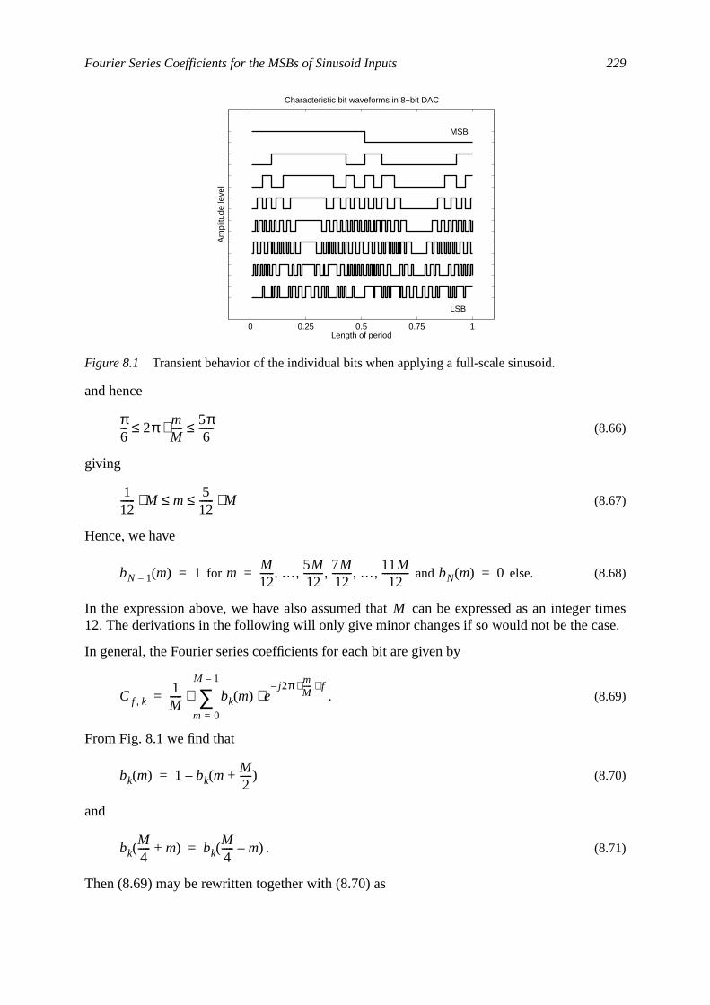
Fourier Series Coefficients for the MSBs of Sinusoid Inputs 229
er timesse.
and hence
(8.66)
giving
(8.67)
Hence, we have
for and else. (8.68)
In the expression above, we have also assumed that can be expressed as an integ12. The derivations in the following will only give minor changes if so would not be the ca
In general, the Fourier series coefficients for each bit are given by
. (8.69)
From Fig. 8.1 we find that
(8.70)
and
. (8.71)
Then (8.69) may be rewritten together with (8.70) as
Figure 8.1 Transient behavior of the individual bits when applying a full-scale sinusoid.
0 0.25 0.5 0.75 1
MSB
LSB
Characteristic bit waveforms in 8−bit DAC
Am
plitu
de le
vel
Length of period
π6--- 2π m
M-----⋅ 5π
6------≤ ≤
112------ M⋅ m
512------ M⋅≤ ≤
bN 1– m( ) 1= mM12------ … 5M
12-------- 7M
12-------- … 11M
12-----------, , , , ,= bN m( ) 0=
M
Cf k,1M----- bk m( ) e
j2π–mM----- f⋅ ⋅
⋅m 0=
M 1–
∑⋅=
bk m( ) 1 bk mM2-----+( )–=
bkM4----- m+( ) bk
M4----- m–( )=
230 Appendices
. (8.72)
Using (8.63) we have the coefficients for the MSB
(8.73)
The normalized power of the tone is given by
. (8.74)
For odd we have that
(8.75)
and for even the coefficients are
. (8.76)
For the second MSB, we have
M Cf k,⋅ bk m( ) ej2π–
mM----- f⋅ ⋅
⋅m 0=
M 2⁄ 1–
∑ bk m( ) ej2π–
mM----- f⋅ ⋅
⋅m M 2⁄=
M 1–
∑+= =
bk m( ) ej2π–
mM----- f⋅ ⋅
⋅m 0=
M 2⁄ 1–
∑ ej2π–
M 2⁄M
------------ f⋅ ⋅bk m
M2-----+( ) e
j2π–mM----- f⋅ ⋅
⋅m 0=
M 2⁄ 1–
∑⋅+= =
bk m( ) bk mM2-----+( ) 1–( ) f⋅+ e
j2π–mM----- f⋅ ⋅
⋅m 0=
M 2⁄ 1–
∑= =
bk m( ) 1 bk m( )–( ) 1–( ) f⋅+[ ] ej2π–
mM----- f⋅ ⋅
⋅m 0=
M 2⁄ 1–
∑=
Cf N,1M----- bN m( ) e
j2π–mM----- f⋅ ⋅
⋅m 0=
M 1–
∑ 1M----- e
j2π–mM----- f⋅ ⋅
m 0=
M2----- 1–
∑ 1M----- 1 e
j2π–M 2⁄
M------------ f⋅ ⋅
–
1 ej2π–
1M----- f⋅ ⋅
–
----------------------------------------⋅= = = =
1M----- e
jπ2---– f⋅
ejπfM------–
----------------
πf2------sin
πfM------sin
--------------⋅ ⋅ 1M-----
πf2------sin
πfM------sin
-------------- ejπf– 1
2--- 1
M-----–
⋅ ⋅= =
Cf N,2 1
M-----
πf2------sin
πfM------sin
--------------⋅
2 πf2------sin2
πf( )2----------------≈=
f
C f N,2 1
πf( )2-------------≈
f
C f N,2 0=
M Cf N 1–,⋅ bN 1– m( ) ej2π–
mM----- f⋅ ⋅
⋅m 0=
M 1–
∑= =
ej2π–
mM----- f⋅ ⋅
m M 12⁄=
5M 12⁄ 1–
∑ ej2π–
mM----- f⋅ ⋅
m M 2⁄=
7M 12⁄ 1–
∑ ej2π–
mM----- f⋅ ⋅
m 11M 12⁄=
M 1–
∑+ += =
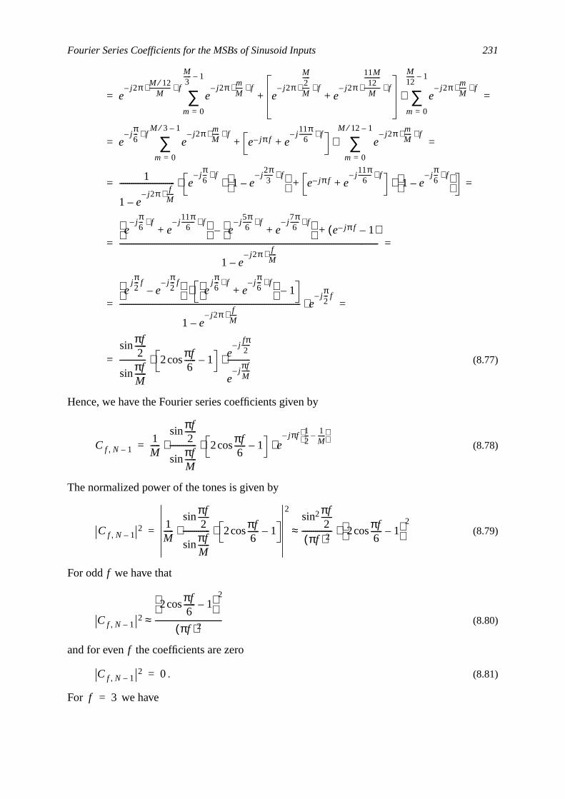
Fourier Series Coefficients for the MSBs of Sinusoid Inputs 231
(8.77)
Hence, we have the Fourier series coefficients given by
(8.78)
The normalized power of the tones is given by
(8.79)
For odd we have that
(8.80)
and for even the coefficients are zero
. (8.81)
For we have
ej2π–
M 12⁄M
--------------- f⋅ ⋅e
j2π–mM----- f⋅ ⋅
m 0=
M3----- 1–
∑ ej2π–
M2-----
M----- f⋅ ⋅
ej2π–
11M12
-----------
M----------- f⋅ ⋅
+ ej2π–
mM----- f⋅ ⋅
m 0=
M12------ 1–
∑⋅+= =
ej–π6--- f⋅
ej2π–
mM----- f⋅ ⋅
m 0=
M 3⁄ 1–
∑ e jπ– f ej11π6
---------– f⋅+ e
j2π–mM----- f⋅ ⋅
m 0=
M 12⁄ 1–
∑⋅+= =
1
1 ej2π–
fM-----⋅
–
----------------------------- ej–π6--- f⋅
1 ej2π3
------– f⋅–
⋅ e jπ– f ej11π6
---------– f⋅+ 1 e
jπ6---– f⋅
– ⋅+⋅= =
ej–π6--- f⋅
ej11π6
---------– f⋅+
ej5π6
------– f⋅e
j7π6
------– f⋅+
– e jπ– f 1–( )+
1 ej2π–
fM-----⋅
–
----------------------------------------------------------------------------------------------------------------------------------------= =
ejπ2--- f
ejπ2---– f
– e
jπ6--- f⋅
ej–π6--- f⋅
+ 1–⋅
1 ej2π–
fM-----⋅
–
----------------------------------------------------------------------------------------------- ejπ2---– f
⋅= =
πf2------sin
πfM------sin
-------------- 2 πf6------cos 1–⋅ e
j–fπ2------
ejπfM------–
------------⋅=
Cf N 1–,1M-----
πf2------sin
πfM------sin
-------------- 2 πf6------cos 1–⋅ e
jπf– 12--- 1
M-----–
⋅ ⋅=
Cf N 1–,2 1
M-----
πf2------sin
πfM------sin
-------------- 2 πf6------cos 1–⋅ ⋅
2 πf2------sin2
πf( )2---------------- 2 πf
6------cos 1–
2⋅≈=
f
C f N 1–,2
2 πf6------cos 1–
2
πf( )2-----------------------------------≈
f
C f N 1–,2 0=
f 3=
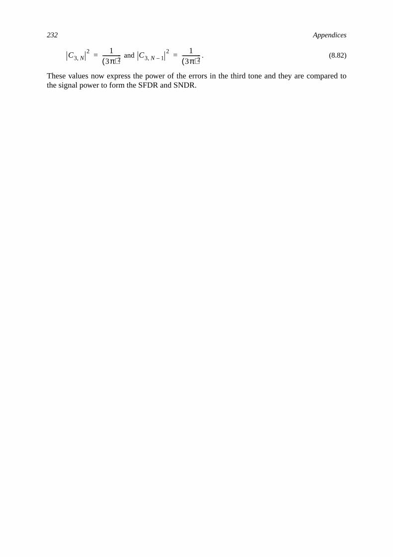
232 Appendices
red to
and . (8.82)
These values now express the power of the errors in the third tone and they are compathe signal power to form the SFDR and SNDR.
C3 N,2 1
3π( )2--------------= C3 N 1–,
2 13π( )2
--------------=
ital8,
ine-4.
mere,”
76-
for
ith
References[1] W.Y. Chen, DSL Simulation Techniques and Standards. Development for Dig
Subscriber Line Systems, Maxmillan Technical Publishing, Indianapolis, IN, USA, 199ISBN 1-57870-017-5.
[2] T. Starr, J.M. Cioffi, and P.J. Silvermann, Understanding Digital Subscriber LTechnology, Prentice Hall, Upper Saddle River, NJ, USA, 1999, ISBN 0-13-780545
[3] “American National Standard for Telecommunications – Network and CustoInstallation Interfaces – Assymetric Digital Subscriber Line (ADSL) Metallic Interfacin draft American National Standard for Telecommunications, ANSI T1E1.4/97-007R6,Jan. 1998.
[4] Future Mobile Standards, private communication, Ericsson Microelectronics AB.[5] J. Rabaey,Digital Integrated Circuits – A Design Perspective, Prentice Hall, Upper
Saddle River, NJ, USA, 1996, ISBN 0-13-394271-6.[6] N.H.E. Weste and K. Eshraghian, Principles of CMOS VLSI Design – A Systems
Perspective, 2nd ed., Addison-Wesley, New York, NY, USA, 1994, ISBN 0-201-5336.
[7] D. A. Johns and K. Martin,Analog Integrated Circuit Design, John Wiley & Sons, NewYork, USA, 1997, ISBN 0-471-14448-7.
[8] B. Razavi,Design of Analog CMOS Integrated Circuits, McGraw-Hill, New York, NY,USA, 2000, ISBN 0-07-238032-2.
[9] R. J. van de Plassche,Integrated Analog-to-Digital and Digital-to-Analog Converters,Kluwer Academic Publishers, Boston, MA, USA, 1994, ISBN 0-7923-9436-4.
[10] H. T. Jensen and I. Galton, “A Low-Complexity Dynamic Element Matching DACDirect Digital Synthesis,”IEEE Trans. on Circuits and Systems II, vol. 45, no. 1, Jan.1998, p. 13-27.
[11] I. Galton, “Spectral Shaping of Circuit Errors in Digital-to-Analog Converters,”IEEETrans. on Circuits and Systems II, vol. 44, no. 10, Oct. 1997, p. 808-17.
[12] J. Yuan and C. Svensson, “New Single-Clock CMOS Latches and Flipflops wImproved Speed and Power Savings,”IEEE J. of Solid-State Circuits, vol. 32, no. 1, Jan.1997, p. 62-9.
233

References 234
s
ew
son,
ust
,
ofent
tio
ncy-of
,
e
in
dish
[13] M. Ismail and T. Fiez,Analog VLSI: Signal and Information Processing, McGraw-Hill,New York, NY, USA, 1994, ISBN 0-07-113387-9.
[14] M. Gustavsson, J.J. Wikner, and N. Tan,CMOS Data Converters for Communication,Kluwer Academic Publishers, Boston, MA, USA, Jan. 2000, ISBN 0-7923-7780-X.
[15] S. Haykin,Digital Communications, John Wiley & Sons, New York, USA, 1988, ISBN0-471-62947-2.
[16] T.M. Cover and J.A. Thomas, Elements of Information Theory, John Wiley & Sons, NYork, USA, 1998, ISBN 0-471-06259-6.
[17] Analog front-end for DSL, Private communication, Ericsson Microelectronics AB.[18] Echo cancellation techniques, Private communication, Ericsson Microelectronics AB.[19] F. Sjöberg, M. Isaksson, P. Deutgen, R. Nilsson, P. Ödling, and P.-O. Börjes
“Performance Evaluation of the Zipper Duplex Method,” inProc. IEEE 1998 Intern.Conf. on Communications, ICC’98, vol. 2, 1998, p. 1035-9.
[20] D.G. Mestdagh, M.R. Isaksson, and P. Ödling, “Zipper VDSL: a Solution for RobDuplex Communication over Telephone Lines,”IEEE Communications Magazine, vol.38, no. 5, May 2000, p. 90-6.
[21] I. Koren, Computer Arithmetic Algorithms, Prentice-Hall, Englewood Cliffs, NJ, USA1993, ISBN 0-13-151952-2.
[22] A. Pacut and K. Hejn, “Analog-to-Digital Converters: Towards a GeneralizationWidrow’s Theorem,” inProc. IEEE 1998 Conf. on Instrumentation and MeasuremTechnology, IMTC’98, vol. 2, 1998, p. 1190-7.
[23] P. Hendriks,“Specifying Communication DACs,” IEEE Spectrum, vol. 34, no. 7, July1997, p. 58-69.
[24] Analog Amp Linearity Characterization via Probability Weighted Mutlitone Power Ra,AN9718, Application note, Intersil, Apr. 1997.
[25] J.J. van de Beek, P. Ödling, S.K. Wilson, and P.O. Börjesson, “Orthogonal FrequeDivision Multiplexing (OFDM),” in Review of Radio Science 1996-99, Intern. UnionRadio Science (URSI), Oxford University Press, UK, 1999.
[26] R.A. Witte, Electronic Test Instruments – Theory and Applications, HP ProfessionalBooks, Prentice Hall, Englewood Cliffs, NJ, USA, 1993, ISBN 0-13-253147-X
[27] J. C. Candy and G. C. Temes,Oversampling Delta-Sigma Data Converters, IEEE Press,New York, NY, USA, 1992, ISBN 0-87942-281-5.
[28] S. Chu and C.S. Burrus, “Multirate Filter Design Using Comb Filters,”IEEE Trans. onCircuits and Systems I, vol. 31, no. 11, Nov. 1988, p. 913-24.
[29] S.R. Norsworthy, R. Schreier, and G.C. Temes,Delta-Sigma Data Converters: TheoryDesign, and Simulation, IEEE Press, NY, USA, ISBN 0-78031-045-4, Nov. 1996.
[30] R. Unbehauen and A. Cichocki,MOS Switched-Capacitor and Continuous-TimIntegrated Circuits and Systems, Springer-Verlag, 1989, ISBN 0-387-50599-7.
[31] S. Wang, M.O. Ahmad, and B.B. Bhattacharrya, “A Novel Cyclic D/A Converter,”Proc. IEEE 1993 Symp. on Circuits and Systems, ISCAS ’93, vol. 2, May 1993, p. 1224-7.
[32] J.J. Wikner and M. Vesterbacka, “D/A Conversion Method and D/A Converter,” Swepatent, 9903500-8, 1999.
[33] J.J. Wikner and M. Vesterbacka, “D/A conversion with Linear-Coded Weights,” inProc.IEEE 2000 Southwest Symp. on Mixed-Signal Design, SSMSD’00, San Diego, CA, USA,Feb. 2000, p. 61-6.
235 References
,” in
,” in
93,
7.
dg
ng
nf.,
sing
eds,
to
e of
es,
r, “A
)
/A
[34] J.J. Wikner and M. Vesterbacka, “Characteristics of Linear-Coded D/A ConvertersProc. IEEE 2000 Southwest Symp. on Mixed-Signal Design, SSMSD’00, San Diego, CA,USA, Feb. 2000, p. 67-72.
[35] M. Vesterbacka and J.J. Wikner, “Characteristics of Linear-Coded D/A ConvertersProc. IEEJ 4th analog VLSI workshop, AVLSIWS’00, Stockholm, Sweden, June 2000.
[36] C. Toumazou, J. B. Hughes, and N. C. Battersby,Switched-Currents: an AnalogueTechnique for Digital Technology, IEE Press, Peter Peregrinus, Stevenage, UK, 19ISBN 0-86341-294-7.
[37] C. Toumazou, F.J. Lidgey, and D.G. Haigh,Analogue IC Design: the Current-ModeApproach, IEE Press, Peter Peregrinus, Stevenage, UK, 1990, ISBN 0-86341-215-
[38] B.J. Tesch and J.C. Garcia, “A Low Glitch 14-b 100MHz D/A Converter,”IEEE J. ofSolid-State Circuits, vol. 32, no. 9, Sept. 1997, p. 1465-9.
[39] C.G. Martinez and S. Simpkins, “A Monolithic 12-Bit Multiplying DAC for NTSC anHDTV Applications, “ in Proc. IEEE 1989 Bipolar Circuits and Technology Meetin,1989, p. 52-5.
[40] P.K. Oborn and D.T. Comer, “A New Digital to Analog Converter Resistor StriArchitecture,” inProc. IEEE 10th Annual Intern. ASIC Conf. and Exhibit, 1997, p. 304-7.
[41] M.J.M. Pelgrom, “A 50 MHz 10-bit CMOS Digital-to-Analog Converter with 75ΩBuffer,” in Digest of Technical Papers 37th IEEE Intern. Solid-State Circuits CoISSCC’90, 1990, p. 200-1, 290, San Fransisco, CA, USA.
[42] V.F. Dias, J.E. Franca, and J.C. Vital, “High-speed Digital-to-Analogue Convertor UPassive Switched-Capacitor Algorithmic Conversion,”Electronics Letters, vol. 24, no.17, Aug. 1988, p. 1063-5.
[43] M.S. Piedade and A. Pinto, “A New Multiplier-Divider Circuit Based on SwitchCapacitor Data Converters,” inProc. IEEE 1990 Intern. Symp. on Circuits and SystemISCAS’90, vol. 3, 1990, p. 2224-7.
[44] H. Träff, T. Holmberg, and S. Eriksson,”Application of Switched Current TechniqueAlgorithmic DA- and AD-Converters,” inProc. IEEE Intern. Symp. on Circuits andSystems, ISCAS’91, June 1991, p. 1549-52.
[45] P. Riffaud-Desgreys, E. Garnier, Ph. Roux, and Ph. Marchegay, “New StructurAlgorithmic DAC in Switched Current Technique,” inProc. 3rd Intern. Conf. onAdvanced A/D and D/A Conversion Techniques and their Applications, Glasgow,Scotland, July 1999, p. 111-4.
[46] AD9774, Data sheet, Analog Devices Inc., 2000.[47] N. Tan, E. Cijvat, and H. Tenhunen,“ Design and Implementation of High-Performanc
CMOS D/A Converter,” InProc. IEEE 1997 Intern. Symp. on Circuits and SystemISCAS’97,Hong Kong, vol. 1, May 1997, p. 421-4.
[48] C.A.A. Bastiaansen, D.W.J. Groeneveld, H.J. Schouwenaars, and H.A.H. Termee10-b 40-MHz 0.8-mm CMOS Current-Output D/A Converter,”IEEE J. of Solid-StateCircuits, vol. 26, no. 7, July 1991, p. 917-21.
[49] C.H. Lin and K. Bult, “A 10-b, 500-MSample/s CMOS DAC in 0.6 mm2,” IEEE J. ofSolid-State Circuits, vol. 33, no. 12, Dec. 1998, p. 1948-58.
[50] S.-Y. Chin and C.-Y. Wu, “A 10-b 125-MHz CMOS Digital-to-Analog Converter (DACwith Threshold-Voltage Compensated Current Sources,”IEEE J. of Solid-State Circuits,vol. 29, no. 11, Nov. 1994, p. 1374-80.
[51] I.H.H. Jørgensen and S.A. Tunheim, “A 10-bit 100MSamples/s BiCMOS DConverter,”Analog Integrated Circuits and Signal Processing, vol. 12, 1997, p. 15-28.
References 236
V
r
ighg
elta
l-to-
.
ques,OS
and
.
ielen,
gI
S.ous
g
AC
[52] N. Tan, “A 1.5-V 3-mW 10-bit 50 MS/s CMOS DAC with Low Distortion and LowIntermodulation in Standard Digital CMOS Process,” inProc. IEEE 1997 CustomIntegrated Circuits Conf., CICC’97, Santa Clara, CA, USA, May 1997, p. 599-602.
[53] J.M. Fournier and P. Senn, “A 130-MHz 8-b CMOS Video DAC for HDTApplications,”IEEE J. of Solid-State Circuits, vol. 26, no. 7, July 1991, p. 1073-6.
[54] A. Fraval and F. Dell’ova, “A 10-bit 70MHz 3.3V CMOS 0.5um D/A Converter foVideo Applications,”IEEE Trans. on Consumer Electronics, vol. 41, no. 3, Aug. 1995,p. 875-9
[55] D.A. Mercer, “Two Approaches To Increasing Spurious Free Dynamic Range in HSpeed DACs,” inProc. IEEE 1993 Bipolar/BiCMOS Circuits and Technology Meetin,1993, p. 80-3.
[56] D. Birru and E. Roza, “Video-Rate D/A Converter Using Reduced Rate Sigma-DModulation,” in Proc. IEEE 1998 Custom Integrated Circuits Conf., CICC’98, 1998,p. 241-4.
[57] B.J. Tesch, P.M. Pratt, K. Bacrania, and M. Sanchez, “A 14-b 125 MSps DigitaAnalog Converter and Bandgap Voltage Reference in 0.5um CMOS,” inProc. IEEEIntern. Symp. on Circuits and Systems 1999, ISCAS’99, Orlando, FL, USA, June 1998, p452-5.
[58] A. Van den Bosch, M. Borremans, J. Vandenbussche, G. Van der Plas, A. MarJ. Bastos, M. Steyaert, G. Gielen, and W. Sansen, “A 12 bit 200 MHz Low Glitch CMD/A Converter,” inProc. IEEE 1998 Custom Integrated Circuits Conf., CICC’98, SanFransisco, CA, USA, 1998, p. 249-52.
[59] A. Marques, J. Bastos, A. Van den Bosch, J. Vandenbussche, M. Steyaert,W. Sansen, “A 12b Accuracy 300MSample/s Update Rate CMOS DAC,” inProc. IEEE1998 Intern. Solid-State Circuits Conf., ISSCC’98, San Fransisco, CA, USA, 1998, p216-7, 440.
[60] J. Vandenbussche, G. Van der Plas, A. Van den Bosch, W. Daerns, G. GM. Steyaert, and W. Sansen, “A 14b 150MSample/s Update Rate Q2 Random WalkCMOS DAC,” in Proc. IEEE 1999 Intern. Solid-State Circuits Conf., ISSCC’99, SanFransisco, CA, USA, 1999, p. 146-7
[61] K. Falaksahi, C.-K. Ken Yang, and B.A. Wooley, “A 14-bit, 5-MHz Digital-to-AnaloConverter Using Multi-bit Sigma-Delta Modulation,” inProc. IEEE 1998 Symp. on VLSCircuits, 1998, p. 164-5.
[62] AD9764, Data sheet, Analog Devices Inc., 2000[63] T.-Y. Wu, C.-T. Jih, J.-C. Chen, and C.-Y. Wu, “A Low Glitch 10-bit 75-MHz CMO
Video D/A Converter,”IEEE J. of Solid-State Circuits, vol. 30, no. 1, Jan. 1995, p. 68-72[64] D.W.J. Groeneveld and H.J. Schouwenaars, “A Dual 3.4V Bitstream Continu
Calibration CMOS D/A Converter with 110 dB Dynamic Range,” inProc. 2nd Intern.Conf. on Advanced A-D and D-A Conversion Techniques and their Applications, UK,1994, p. 42-7,
[65] D. Mercer, “A 16-b D/A Converter with Increased Spurious Free Dynamic Range,”IEEEJ. of Solid-State Circuits, vol. 29, Dec. 1994, p. 1180-5.
[66] M.J.M. Pelgrom and M. Roorda, “An Algorithmic 15-bit CMOS Digital-to-AnaloConverter,”IEEE J. of Solid-State Circuits, vol. 23, no. 6, Dec. 1988, p. 1402-5.
[67] A.R. Bugeja, B.-S. Song, P.L. Rakers, and S.F. Gillig, “A 14-b, 100-MS/s CMOS DDesigned for Spectral Performance”,IEEE J. of Solid-State Circuits, vol. 34, no. 12, Dec.1999, p. 1719-32.
237 References
OS
it
n ofg
tal
o 16-
or
AC00,
AC
of
or’98
ent
el of
s,471-
2.in x/
2,
L
[68] M.J.M Pelgrom, A.C.J. Duinmaijer, and A.P.G. Welbers, “Matching Properties of MTransistors,”IEEE J. of Solid-State Circuits, vol. 24, no. 5, Oct. 1989, p. 1433-9.
[69] T. Miki, Y. Nakamura, M. Nakaya, S. Asai, Y. Akasaka, Y. Horiba, “An 80 MHz 8-bCMOS D/A Converter,”IEEE J. of Solid-State Circuits, vol. 21, Dec. 1986, p. 983-8.
[70] J. Bastos, M. Steyaert, A. Pergoot, and W. Sansen, “Mismatch CharacterizatioSubmicron MOS Transistors,”,Analog Integrated Circuits and Signal Processin,vol. 12, no. 2, Feb. 1997, p. 95-106.
[71] H. Tuinhout, M.J.M. Pelgrom, R. Penning de Vries, and M. Vertregt, “Effects of MeCoverage on MOSFET Matching,” inProc. Intern. Electron Devices Meeting, IEDM’96,San Fransisco, CA, USA, Dec. 1996, p. 735-8.
[72] H.J. Schouwenaars, D.W.J. Groeneveld, and H.A.H. Termeer, “A Low-Power Sterebit CMOS D/A Converter for Digital Audio,”IEEE J. of Solid-State Circuits, vol. 23,Dec. 1988, p. 1290-7.
[73] J.J. Wikner and N. Tan, “Modeling of CMOS Digital-to-Analog Converters fTelecommunication,”IEEE Trans. on Circuits and Systems II,vol..46, no. 5, May 1999,p. 489-99.
[74] K.O. Andersson and J.J. Wikner, “Characterization of a CMOS Current-Steering Dusing State-Space Models,“ inProc. IEEE Midwest Symp. on Circuits and Systems 20MWSCAS’00, Lansing, MI, USA, Aug. 2000.
[75] K.O Andersson, N.U. Andersson, and J.J. Wikner, “Spectral Shaping of DNonlinearity Errors through Modulation of Expected Errors,” to appear inProc. IEEE2001 Intern. Symp. on Circuits and Systems, ISCAS’01, Sydney, Australia, May 6-9,2001.
[76] J.J. Wikner and N. Tan, “Influences of Circuit Imperfections on the PerformanceDACs,” Analog Integrated Circuits and Signal Processing, no. 1, Jan. 1999.
[77] J.J. Wikner and N. Tan, “Modelling of CMOS Digital-to-Analog Converters fTelecommunication,” inProc. IEEE Symp. on Circuits and Systems 1998, ISCAS,Monterey, CA, USA, May/June 1998, p. 25-8.
[78] K.O. Andersson and J.J. Wikner, “Modeling of the Influence of Graded ElemMatching Errors in CMOS Current-Steering DACs,” inProc. 17th NorChip Conf., Oslo,Norway, Nov. 8-9, 1999.
[79] J. Vandenbussche, G. Van Der Plas, G. Gielen, and W. Sansen, “Behavioral ModReusable D/A Converters,”IEEE Trans. on Circuits and Systems II, vol. 46, no. 10, Oct.1999, p. 1323-6.
[80] N.J. Fliege, Multirate Digital Signal Processing: Multirate Systems, Filter BankWavelets, John Wiley & Sons, Chichester, West Sussex, England, 1994, ISBN 0-93976-5.
[81] L. Wanhammar,DSP Integrated Circuits, Academic Press, 1998, ISBN 0-127-34530-[82] B.G. Henriques and J.E. Franca, “High-speed D/A Conversion With Linear Phase S
x Compensation,” inProc. IEEE Symp. on Circuits and Systems 1993, ISCAS’93, vol. 2,1993, p. 1204-7.
[83] G. Eriksson,Interpolation Filters in OSDACs for DSL Applications, Master Thesis,LiTH-ISY-EX-3151, Linköping University, 2001.
[84] M. Lövgren, Sigma-delta Modulators in DACs, Master Thesis, LiTH-ISY-EX-315Linköping University, 2001.
[85] J.J. Wikner, Y. Gao, and N. Tan, “D/A Conversion Interface Design for DMT-ADSApplications,”IEEE Magazine of Circuits & Devices, vol. 1, no. 6, Nov. 1998, p. 7-13.
References 238
s,”
-A
t-
stem
D/A,
D/Al
-
rs,
ror-
/A
atch
rear
rent--
tion
[86] C. Dunn and M. Sandler, “Adaptive Sigma-Delta Modulation for use in DACElectronics Letters, vol. 32, no. 10, May 1996, p. 867-8.
[87] Y. Matsuya, K. Uchimura, A. Iwata, and T. Kaneko, “A 17 bit Oversampling DConversion Technology Using Multistage Noise Shaping,”IEEE J. of Solid-StateCircuits, vol. 24, no. 4, Aug. 1989, p. 969-75.
[88] Y. Zhou and J. Yuan, “An 8-bit, 100 MHz Low Glitch Interpolation DAC,” inProc. 18thNorChip Conf., Turku, Finland, Nov. 2000.
[89] D.K. Su and B.A. Wooley, “A CMOS Oversampling D/A Converter with a CurrenMode Semi-Digital Reconstruction Filter,” inProc. IEEE 1993 Intern. Solid-StateCircuits Conf., ISSCC’93, San Fransisco, CA, USA, Feb. 1993, p. 230-1.
[90] B.G. Henriques and J.E. Franca, “A High-Speed Programmable CMOS Interface SyCombining D/A Conversion and FIR,”IEEE J. of Solid-State Circuits, vol. 29, no. 8, Aug.1994, p. 972-7.
[91] Matlab Reference Manual, Mathworks, Dec. 1999.[92] Y. Gao, J. J. Wikner, and H. Tenhunen, “Design and Analysis of an Oversampling
Converter for DMT-ADSL Systems,” inProc. IEEJ 3rd Analog VLSI WorkshopAVLSIWS’99, Taiwan, May, 1999.
[93] Y. Gao, J.J. Wikner, and H. Tenhunen, “Design and Analysis of an OversamplingConverter in DMT-ADSL Systems,” to appear inAnalog Integrated Circuits and SignaProcessing J., 2001.
[94] J.-W. Kim, B.-M. Min, J.-S. Yoo, and S.-W. Kim, “An Area-Efficient Sigma-Delta DACwith a Current-Mode Semidigital IFIR Reconstruction Filter,” inProc. 1998 IEEE Intern.Symp. on Circuits and Systems, ISCAS’98, Monterey, CA, USA, May/June, 1998, p. 3447.
[95] K.-H. Ryu, K.S. Yoon, and H.K. Min, “Design of a 3.3 V 12 bit CMOS D/A convertewith a high linearity,” in Proc.IEEE 1998 Midwest Symp. on Circuits and SystemMWSCAS’98, 1998, p. 538-41.
[96] Y. Cong and R.L. Geiger, “Switching-Sequence Optimization for Gradient ErCompensation in Thermometer-Decoded DAC Array,”IEEE Trans. on Circuits andSystems II, vol. 47, no. 7, July 2000, p. 585-95.
[97] R.J. Romanczyk and B.H. Leung, “BiCMOS Circuits for High Speed Current Mode DConverters,”IEEE J. of Solid-State Circuits, vol. 30, no. 8, Aug. 1995, p. 923-34.
[98] A. van den Bosch, M. Steyaert, and W. Sansen, “The Extraction of Transistor MismParameters: The CMOS Current-Steering D/A Converter as a Test Structure,” inProc.IEEE 2000 Intern. Symp. on Circuits and Systems, ISCAS’00, vol. 2, Geneva,Switzerland, May 2000, p. 745-8.
[99] M. Otsuka, S. Ichiki, T. Tskuada, T. Matsuura, and K. Maio, “Low-Power, Small-A10bit D/A Converter for Cell-Based IC,” inProc. 1995 IEEE Symp. on Low PoweElectronics, 1995, p. 66-7.
[100] B. E. Jonsson, “Design of Power Supply Lines in High-Performance SI and CurMode Circuits,” inProc. 15th Norchip Conf., Tallinn, Estonia, Nov. 10-11, 1997, p. 24550.
[101] www.nallatech.com, Product information, Dec. 1999.[102] AD6644, Data sheet, Analog Devices Inc., 2000.[103] K. Kitamura and K. Rondo, “Distortion Compensation Characteristics of Pre-Distor
Circuit for Private Mobile Radio,”Electronics Letters, vol. 36, no. 20, Oct. 2000,p. 1675-6.
239 References
ror
llys,
rtion
mss
in
ish
pingd
AC
ed
in000
entd-
ing
e-s,
/AI
,”
[104] J.-H. Han and S. Nam, “Power Amplifier Linearisation Using Post-Distortion ErCanceller Based on Complex Envelope Transfer Characteristics,”Electronics Letters,vol. 36, no. 19, Sept. 2000, p. 1665-6.
[105] A. Bauer and W. Schwarz, “Circuit Analysis and Optimization with AutomaticaDerived Volterra Kernels,” inProc. IEEE 2000 Intern. Symp. on Circuits and SystemISCAS’00, vol. 1, Geneva, Switzerland, 2000, p. 491-4.
[106] P. Wambacq, G.G.E. Gielen, P.R. Kinget, and W. Sansen, “High-Frequency DistoAnalysis of Analog Integrated Circuits,”IEEE Trans. on Circuits and Systems II, vol. 46,no. 3, March 1999, p. 335-45.
[107] S. Orcioni, “Approximation and Analog Implementation of Nonlinear SysteRepresented by Volterra Series,” inProc. 6th IEEE Intern. Conf. on Electronics, Circuitand Systems, 1999, ICECS’99, vol. 2, 1999, p. 1109-13.
[108] M. Karlsson Rudberg, “ADC Offset Identification and Correction in DMT Modems,”Proc. IEEE 2000 Intern. Conf. on Circuits and Systems, ISCAS’00, vol. 4, Geneva,Switzerland, 2000, p. 677-80.
[109] J.-E. Eklund and M. Karlsson Rudberg, “Correction of Static Errors in ADCs,” Swedpatent, 9902000-0, May 1999.
[110] D.P. Scholnik and J.O. Coleman, “Vector Delta-Sigma Modulation with Integral Shaof Hardware-Mismatch Errors,” inProc. IEEE 2000 Intern. Symp. on Circuits anSystems, ISCAS’00, Geneva, Switzerland, 2000, p. 677-80.
[111] K.O. Andersson, N.U. Andersson, and J.J. Wikner, “Spectral Shaping of DNonlinearity Errors through Modulation of Expected Errors,” to appear inProc. IEEE2001 Intern. Symp. on Circuits and Systems, ISCAS’01, Sydney, Australia, May, 2001.
[112] A. Biman and D. G. Nairn, “Trimming of Current Mode DACs by Adjusting Vt,” in Proc.1996 IEEE Intern. Symp. on Circuits and Systems, ISCAS’96, vol. 1, Atlanta, GA, USA,May 1996, p. 33-6.
[113] S. Boiocchi, S. Brigati, G. Caiulo, and F. Maloberti, “Self-Calibration in High SpeCurrent Steering CMOS D/A Converters,” inProc. IEE 2nd Intern. Conf. on ‘AdvancedA-D and D-A Conversion Techniques and their Applications’, London, UK, 1994, p. 148-52.
[114] B. Vargha and I. Zoltan, “Calibration Algorithm for Current-Output R-2R Ladders,”Proc. IEEE 17th Instrumentation and Measurement Technology Conf. 2000, IMTC 2,vol. 2, 2000, p. 753-8.
[115] N.U. Andersson and J.J. Wikner, “A Strategy of Implementing Dynamic ElemMatching in Current-Steering DACs,“ inProc. IEEE 2000 Southwest Symp. on MixeSignal Design, SSMSD’00, San Diego, CA, USA, Feb. 2000, p. 51-6.
[116] N.U. Andersson and J.J. Wikner, “Comparison of Different Dynamic Element MatchTechniques for Wideband CMOS DACs,” inProc. 17th NorChip Conf., Oslo, Norway,Nov. 1999.
[117] H. Lin, J. Barreiro da Silva, B. Zhang, and R. Schreier, “Multi-Bit DAC with NoisShaped Element Mismatch,” inProc. 1996 IEEE Intern. Symp. on Circuits and SystemISCAS’96, vol. 1, Atlanta, GA, USA, May 1996, p. 235-8.
[118] R.T. Baird and T.S. Fiez, “Linearity Enhancement of Multibit Delta-Sigma A/D and DConverters Using Data Weighted Averaging,”IEEE Trans. on Circuits and Systems I,vol. 42, no. 12, Dec. 1995, p. 753-62.
[119] A. Keady and C. Lyden, “Tree Structure for Mismatch Noise-Shaping Multibit DACElectronics Letters, vol. 33, no. 17, Aug. 1997, p. 1431-2.
References 240
amicn
ith
ment
litch
mic
D/A’01
igh
[120] J.W. Bruce and P. Stubberud,“Generalized Cube Networks for Implementing DynElement Matching Digital-to-Analog Converters,” inProc. IEEE 1998 Midwest Symp. oCircuits and Systems, MWSCAS’98, 1999, p. 522-5.
[121] R. Adams, K.Q. Nguyen, and K. Sweetland, “A 113-dB SNR Oversampling DAC wSegmented Noise-Shaped Scrambling,”IEEE J. of Solid-State Circuits, vol. 33, no. 12,Dec. 1998, p. 1871-8.
[122] N.U. Andersson, M. Vesterbacka, J.J. Wikner, and M. Karlsson Rudberg, "Improveof Segmented DACs", Swedish patent 0001917-4 pending, May 2000
[123] M. Karlsson Rudberg, M. Vesterbacka, N.U. Andersson, and J.J. Wikner, “GMinimization and Dynamic Element Matching in D/A Converters,” inProc. IEEE 7thIntern. Conf. on Electronics, Circuits, and Systems, ICECS’00, Beirut, Lebanon, Dec.2000.
[124] M. Vesterbacka, M. Karlsson Rudberg, J.J. Wikner, and N.U. Andersson, “DynaElement Matching in D/A Converters with Restricted Scrambling,” inProc. IEEE 7thIntern. Conf. on Electronics, Circuits, and Systems, ICECS’00, Beirut, Lebanon, Dec.2000.
[125] M. Vesterbacka and J.J. Wikner, "Design of Encoders for Linear-CodedConverters". Submitted toIEEE 2001 Intern. Symp. on Circuits and Systems, ISCAS,Sydney, Australia, May 2001.
[126] A. van den Bosch, M. Steyaert, and W. Sansen, “SFDR-Bandwidth Limitations for HSpeed High Resolution Current Steering CMOS D/A Converters,” inProc. 6th IEEEIntern. Conf. on Electronics, Circuits and Systems, vol. 3, 1999, p. 1193-6.
Index
AAdmittance ratio 109ADSL, Asymmetric digital subscriber line 11AFE, Analog front end 12
BBias current 148
CCalibration technique 197CAP, Carrierless amplitude phase modulation11Capacitance ratio 91CFT, Clock feedthrough 47, 141Common-centroid layout 87Conductance ratio 91, 128Converter
Digital-to-analog 26Crest factor 54Crosstalk 22
FEXT,Far-end 22NEXT, Near-end 22
Current source matching 137
DD/A converters
Algorithmic 71Binary-weighted 68Charge-redistribution 74Current-steering 73, 128Direct encoded 69Dual linear-coded 214Hybrid 70Interpolating 57Linear-coded 70, 209Nyquist-rate 56One-bit 174Oversampling 62Pipelined algorithmic 72R-2R ladder 74Resistor-string 75Segmented 131SI algorithmic 75Signed-digit coded 215Thermometer-coded 68
DAC, Digital-to-analog converter 26dBFS 48DEM, Dynamic element matching 199
DMT, Discrete multi-tone 13, 180DNL, Differential nonlinearity 37, 99DSL, Digital subscriber line 11Duplex 11Dynamic element matching
FRDEM, Full-randomization 203NSDEM, Noise-shaping 205PRDEM, Partial-randomization 204Reduced glitching 205
Dynamic randomization 200
EEcho cancelling 13Element matching 84ENOB, Effective number of bits 51
FFEXT, Far-end crosstalk 22Filter
Image-rejection 56FIR, Finite-length impulse response 58Full-duplex 11
GGain error 35GCN, Generalized cubic network 206Glitch 45, 123, 212Graded mismatch 85
HHalf-duplex 11HD, Harmonic distortion 50, 100, 118
IIFIR, interpolated FIR 58IIR, Infinite-length impulse response 58Image-rejection filter 27, 56, 177, 184IMD, Intermodulation distortion 52Impedance ratio 109INL, Integral nonlinearity 37, 99Interdigitized layout 87Interpolated FIR filter 176Interpolating D/A converters 57Interpolation 57Interpolator 164IPF, Interpolation filter 57, 164, 180IQ diagram 9
i
Index ii
MMeasurement 150Miller effect 47Mismatch 113, 129, 148
Graded 85Stochastic 86
Mixed-signal design 145Modulation 9
DMT, Discrete multi-tone 13PAM, Pulse-amplitude modulation 26QAM, Quadrature amplitude modulation 9
ModulatorError-feedback 63, 169MASH, Multi-stage 173MF, Multiple-feedback 65, 171, 182Multi-bit 64, 170Noise-shaping 62, 169, 182One-bit 64, 170Signal-feedback 62, 169
Monotonicity 39Moving average filter 167MSB segmentation circuit 144MTPR, Multi-tone power ratio 51Multi-rate filtering 165Multi-stage interpolation 165
NNEXT, Near-end crosstalk 22Noise 110Noise bandwidth 110Noise-shaping modulators 62NTF, Noise transfer function 62, 171Nyquist-rate D/A converters 56
OOffset error 34OSDAC, Oversampling D/A converters 62OSR, Oversampling ratio 58, 164
PPAM, Pulse-amplitude modulation 26PAR, Peak-to-average ratio 15, 54Parasitic resistance 107Performance
Dynamic 42Static 31
Poissons formula 26
Post-distortion circuit 192PR, Power ratio 97PRBS, Pseudo-random binary sequence 201Pre-distortion circuit 192, 193Prefix 19PSD, Power spectral density 57
QQAM, Quadrature amplitude modulation 9Quantization
Noise 31Non-uniform 40Uniform 32
RR2Z, Return-to-zero 143, 217
SScrambler 200Semi-digital FIR filter 175, 184, 185Settling-time error 95SFDR, Spurious-free dynamic range51, 105, 120,
122Signed-digit code 215Simplex 11Sinc filter 167SNDR, Signal-to-noise-and-distortion ratio50,
102, 116, 122, 227SNR, Signal-to-noise ratio 33, 50, 112Splitter filter 12SQNR, Signal-to-quantization noise ratio 33STF, Signal transfer function 62, 171Stochastic mismatch 86SUFR, Signal-to-update frequency ratio 46Switch memory 143Switch on-conductance 88Switch on-resistance 139Switch signal generator 142
TTHD, Total harmonic distortion 50Time ratio 92Twisted-pair 20
UUnit current source 134, 147, 187, 198


DissertationsDivision of Electronics Systems
Department of Electrical EngineeringLinköpings universitet
Sweden
rs,ni-
l Fil-ings
ingwe-
ers,ing
Vesterbacka, M.: On Implementation of Maximally Fast Wave Digital FilteLinköping Studies in Science and Technology, Diss. No. 487, Linköpings Uversity, Sweden, June 1997.
Johansson, H.: Synthesis and Realization of High-Speed Recursive Digitaters, Linköping Studies in Science and Technology, Diss. No. 534, LinköpUniversity, Sweden, May 1998.
Gustavsson, M.: CMOS A/D Converters for Telecommunications, LinköpStudies in Science and Technology, Diss. No. 552, Linköpings University, Sden, Dec 1998.
Palmkvist K.: Studies on the the Design and Implementation of Digital FiltLinköping Studies in Science and Technology, Dissertation. No. 583, LinköpUniversity, Sweden, June 1999.