Embed Size (px)
Citation preview

Nyquist Digital to Analog ConvertersNyquist Digital to Analog ConvertersTuesday, February 22nd, 9:15 – 11:10
Snorre Aunet ([email protected])Nanoelectronics group
Department of InformaticsUniversity of Oslo
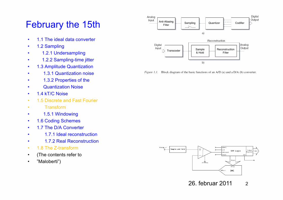
February the 15th• 1.1 The ideal data converter• 1.2 Sampling• 1.2.1 Undersamplingp g• 1.2.2 Sampling-time jitter• 1.3 Amplitude Quantization• 1.3.1 Quantization noise• 1.3.2 Properties of the• Quantization Noise• 1.4 kT/C Noise• 1 5 Discrete and Fast Fourier• 1.5 Discrete and Fast Fourier• Transform• 1.5.1 Windowing• 1.6 Coding Schemesg• 1.7 The D/A Converter• 1.7.1 Ideal reconstruction• 1.7.2 Real Reconstruction• 1.8 The Z-transform• (The contents refer to • ”Maloberti”)
226. februar 2011
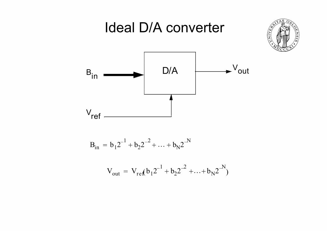
Ideal D/A converter
D/ABinVout
Vrefref
1 2 NBin b12 1– b22 2– … bN2 N–+ + +=
1 2 NVout Vref b12 1– b22 2– … bN2 N–+ + +( )=
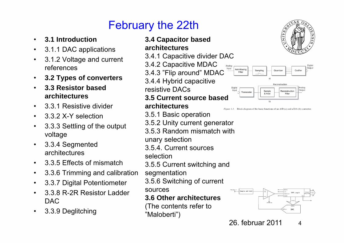
February the 22th• 3 1 Introduction 3 4 Capacitor based• 3.1 Introduction• 3.1.1 DAC applications• 3.1.2 Voltage and current
f
3.4 Capacitor basedarchitectures3.4.1 Capacitive divider DAC3.4.2 Capacitive MDACreferences
• 3.2 Types of converters• 3.3 Resistor based
hit t
3.4.2 Capacitive MDAC3.4.3 ”Flip around” MDAC3.4.4 Hybrid capacitiveresistive DACs
architectures• 3.3.1 Resistive divider• 3.3.2 X-Y selection
3.5 Current source basedarchitectures3.5.1 Basic operation3 5 2 Unity current generator• 3.3.3 Settling of the output
voltage• 3.3.4 Segmented
3.5.2 Unity current generator3.5.3 Random mismatch withunary selection3 5 4 Current sources
architectures• 3.3.5 Effects of mismatch• 3.3.6 Trimming and calibration
3.5.4. Current sourcesselection3.5.5 Current switching and segmentation
• 3.3.7 Digital Potentiometer• 3.3.8 R-2R Resistor Ladder
DAC
3.5.6 Switching of currentsources3.6 Other architectures(Th t t f t
• 3.3.9 Deglitching
426. februar 2011
(The contents refer to ”Maloberti”)
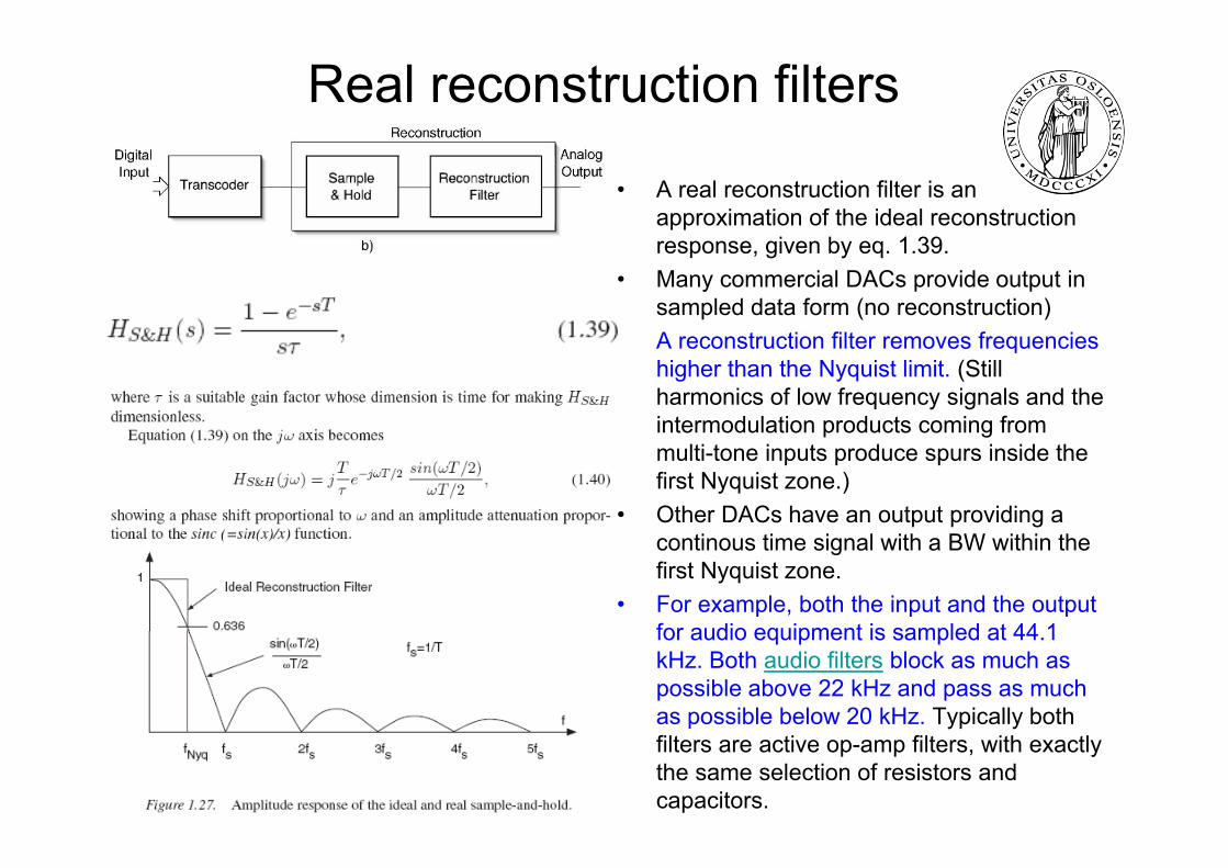
Real reconstruction filters
• A real reconstruction filter is an approximation of the ideal reconstruction
i b 1 39response, given by eq. 1.39.• Many commercial DACs provide output in
sampled data form (no reconstruction)A t ti filt f i• A reconstruction filter removes frequencieshigher than the Nyquist limit. (Still harmonics of low frequency signals and theintermodulation products coming from p gmulti-tone inputs produce spurs inside thefirst Nyquist zone.)
• Other DACs have an output providing a continous time signal with a BW within thefirst Nyquist zone.
• For example, both the input and the output for audio equipment is sampled at 44 1for audio equipment is sampled at 44.1 kHz. Both audio filters block as much as possible above 22 kHz and pass as much as possible below 20 kHz. Typically both filters are active op-amp filters, with exactly the same selection of resistors and capacitors.
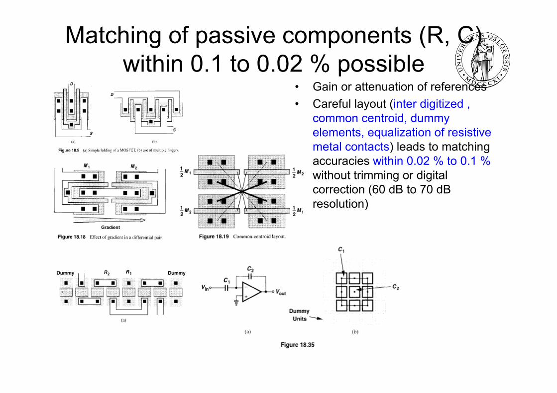
Matching of passive components (R, C) within 0 1 to 0 02 % possiblewithin 0.1 to 0.02 % possible
• Gain or attenuation of references• Careful layout (inter digitized ,Careful layout (inter digitized ,
common centroid, dummy elements, equalization of resistivemetal contacts) leads to matching ) gaccuracies within 0.02 % to 0.1 % without trimming or digital correction (60 dB to 70 dB resolution)
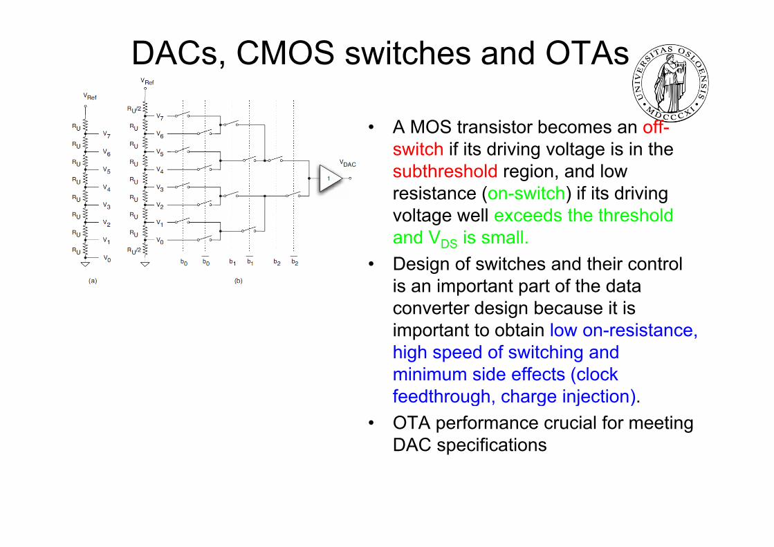
DACs, CMOS switches and OTAs
• A MOS transistor becomes an off-switch if its driving voltage is in theswitch if its driving voltage is in thesubthreshold region, and lowresistance (on-switch) if its driving
lt ll d th th h ldvoltage well exceeds the thresholdand VDS is small.
• Design of switches and their controlgis an important part of the data converter design because it is important to obtain low on-resistance,important to obtain low on resistance, high speed of switching and minimum side effects (clockfeedthrough charge injection)feedthrough, charge injection).
• OTA performance crucial for meetingDAC specifications
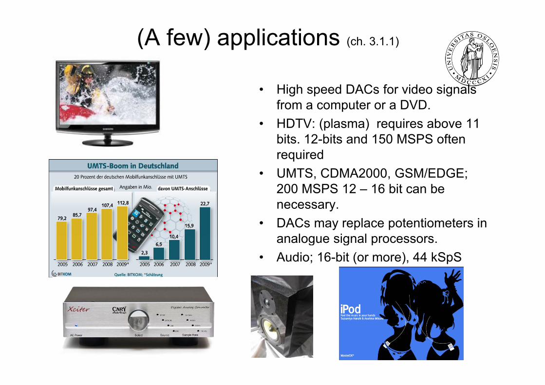
(A few) applications (ch. 3.1.1)
• High speed DACs for video signals from a computer or a DVDfrom a computer or a DVD.
• HDTV: (plasma) requires above 11 bits. 12-bits and 150 MSPS oftenrequired
• UMTS, CDMA2000, GSM/EDGE; 200 MSPS 12 – 16 bit can be200 MSPS 12 16 bit can be necessary.
• DACs may replace potentiometers in analogue signal processorsanalogue signal processors.
• Audio; 16-bit (or more), 44 kSpS
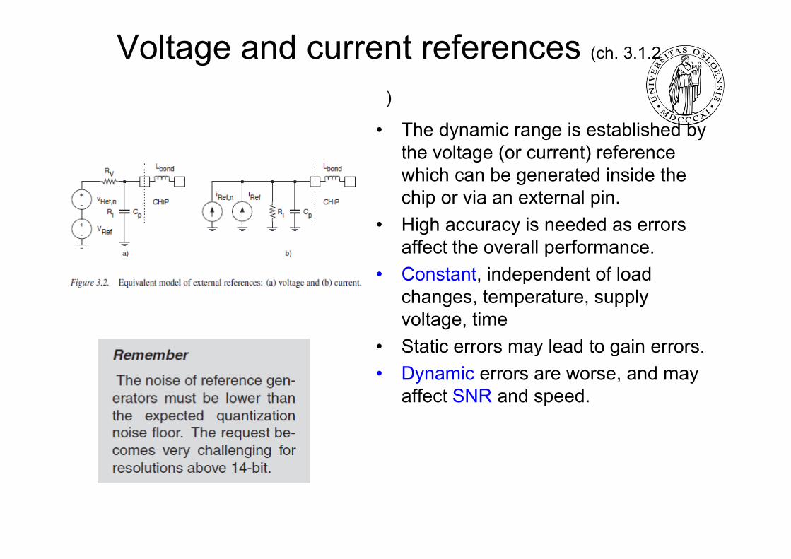
Voltage and current references (ch. 3.1.2
)
• The dynamic range is established by the voltage (or current) referencethe voltage (or current) referencewhich can be generated inside thechip or via an external pin.
• High accuracy is needed as errorsaffect the overall performance.
• Constant, independent of loadConstant, independent of loadchanges, temperature, supplyvoltage, timeStatic errors may lead to gain errors• Static errors may lead to gain errors.
• Dynamic errors are worse, and mayaffect SNR and speed.
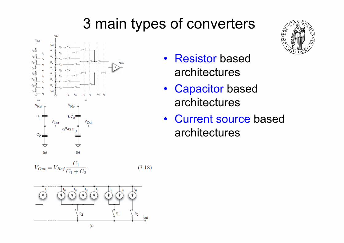
3 main types of converters
• Resistor basedarchitectures
• Capacitor basedparchitectures
• Current source basedCurrent source basedarchitectures
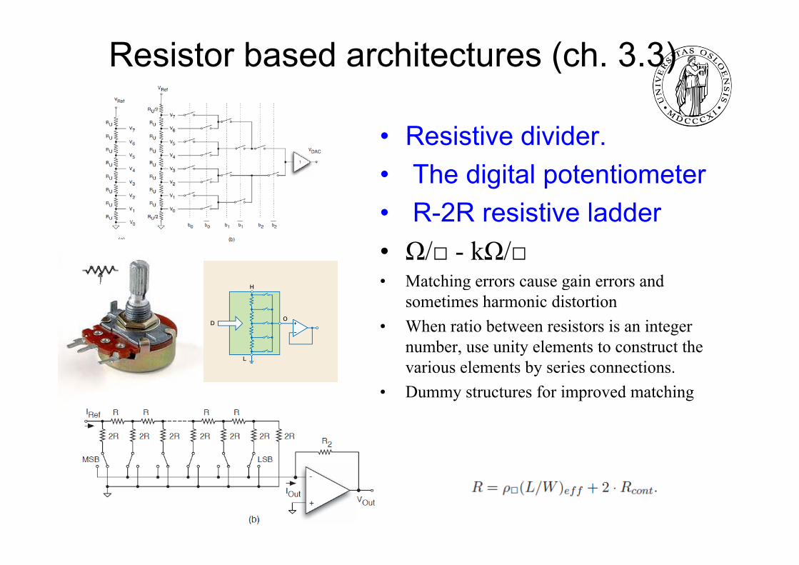
Resistor based architectures (ch. 3.3)
• Resistive divider.• The digital potentiometer• R-2R resistive ladderR 2R resistive ladder• Ω/ - kΩ/• Matching errors cause gain errors and• Matching errors cause gain errors and
sometimes harmonic distortion• When ratio between resistors is an integer
number use unity elements to construct thenumber, use unity elements to construct thevarious elements by series connections.
• Dummy structures for improved matching
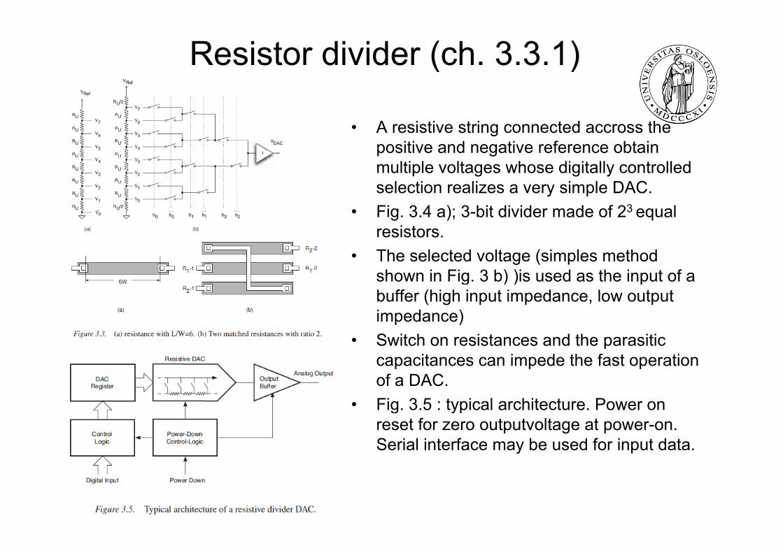
Resistor divider (ch. 3.3.1)
• A resistive string connected accross thepositive and negative reference obtainpositive and negative reference obtainmultiple voltages whose digitally controlledselection realizes a very simple DAC.
• Fig 3 4 a); 3-bit divider made of 23 equalFig. 3.4 a); 3 bit divider made of 2 equalresistors.
• The selected voltage (simples methodshown in Fig 3 b) )is used as the input of ashown in Fig. 3 b) )is used as the input of a buffer (high input impedance, low output impedance)
• Switch on resistances and the parasitic• Switch on resistances and the parasiticcapacitances can impede the fast operationof a DAC.
• Fig 3 5 : typical architecture Power on• Fig. 3.5 : typical architecture. Power onreset for zero outputvoltage at power-on. Serial interface may be used for input data.
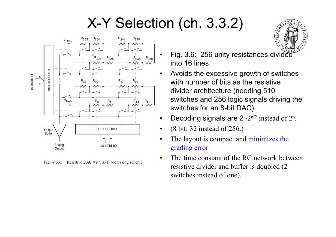
X-Y Selection (ch. 3.3.2)
• Fig. 3.6: 256 unity resistances dividedinto 16 linesinto 16 lines.
• Avoids the excessive growth of switcheswith number of bits as the resistivedivider architecture (needing 510divider architecture (needing 510 switches and 256 logic signals driving theswitches for an 8-bit DAC).
• Decoding signals are 2 ·2n/2 instead of 2n• Decoding signals are 2 ·2 instead of 2 .• (8 bit: 32 instead of 256.)• The layout is compact and minimizes the
digrading error• The time constant of the RC network between
resistive divider and buffer is doubled (2 switches instead of one).
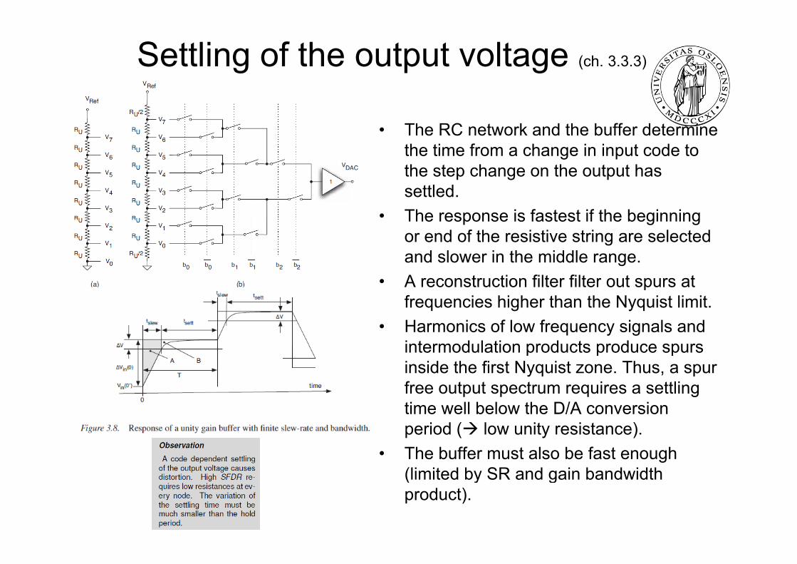
Settling of the output voltage (ch. 3.3.3)
• The RC network and the buffer determinethe time from a change in input code tothe time from a change in input code to the step change on the output has settled.
• The response is fastest if the beginningThe response is fastest if the beginningor end of the resistive string are selectedand slower in the middle range.
• A reconstruction filter filter out spurs at• A reconstruction filter filter out spurs at frequencies higher than the Nyquist limit.
• Harmonics of low frequency signals and intermodulation products produce spursintermodulation products produce spursinside the first Nyquist zone. Thus, a spurfree output spectrum requires a settlingtime well below the D/A conversiontime well below the D/A conversionperiod ( low unity resistance).
• The buffer must also be fast enough(limited by SR and gain bandwidth(limited by SR and gain bandwidthproduct).
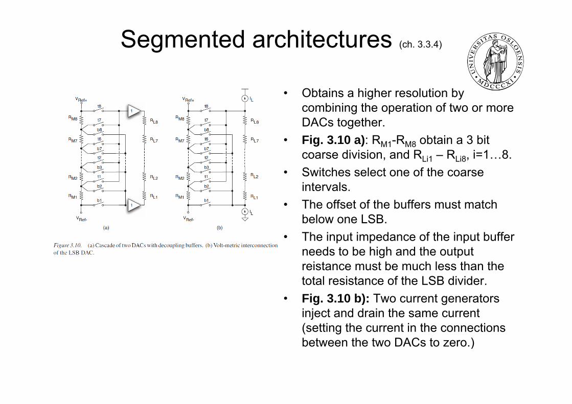
Segmented architectures (ch. 3.3.4)
• Obtains a higher resolution by combining the operation of two or morecombining the operation of two or more DACs together.
• Fig. 3.10 a): RM1-RM8 obtain a 3 bit coarse division and RLi1 – RLi8 i=1 8coarse division, and RLi1 RLi8, i 1…8.
• Switches select one of the coarseintervals.The offset of the b ffers m st match• The offset of the buffers must match below one LSB.
• The input impedance of the input buffer d t b hi h d th t tneeds to be high and the output
reistance must be much less than thetotal resistance of the LSB divider.Fi 3 10 b) T• Fig. 3.10 b): Two current generators inject and drain the same current(setting the current in the connectionsb t th t DAC t )between the two DACs to zero.)

Effect of the mismatch (ch. 3.3.5)
• Global error and local fluctuations ofparametersparameters
• The error depends on accumulation ofmismatches and is zero at the two endsof the stringof the string.
• Problematic when errors are correlatedand accumulate to a large INL.Fig 3 11 8 bit DAC ith ά∆X +/ 10 4• Fig.3.11: 8-bit DAC with ά∆X = +/-10-4
• (∆X is the spacing between unity elements.)(curves a) and b)) Max INL±0.8 LSB.
• Fig. 3.11 c) has a resistive divider foldedaround it’s midpoint, where the INL becomeszero. The max INL is reduced to ¼.
• Better results are obtained with multiple folding and suitably designed layouts.
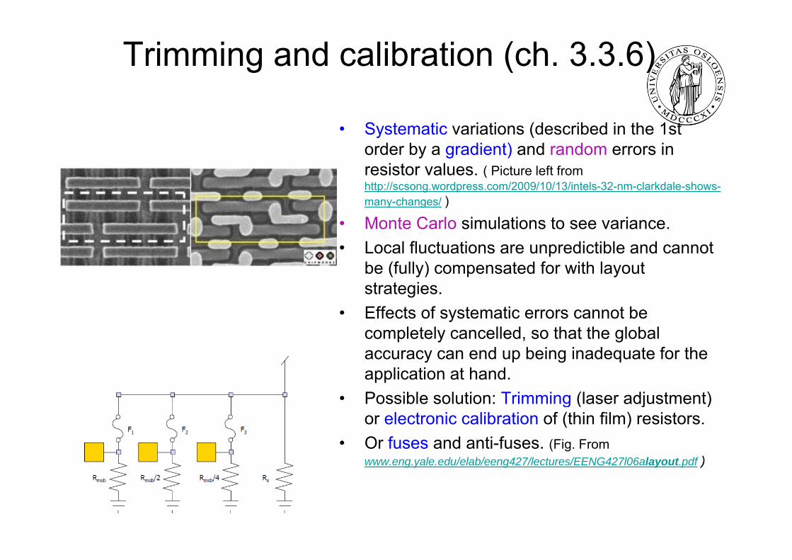
Trimming and calibration (ch. 3.3.6)
• Systematic variations (described in the 1st order by a gradient) and random errors inorder by a gradient) and random errors in resistor values. ( Picture left from http://scsong.wordpress.com/2009/10/13/intels-32-nm-clarkdale-shows-many-changes/ )
• Monte Carlo simulations to see variance.• Local fluctuations are unpredictible and cannot
be (fully) compensated for with layout strategies.
• Effects of systematic errors cannot be completely cancelled, so that the global accuracy can end up being inadequate for theapplication at hand.
• Possible solution: Trimming (laser adjustment) g ( j )or electronic calibration of (thin film) resistors.
• Or fuses and anti-fuses. (Fig. From www.eng.yale.edu/elab/eeng427/lectures/EENG427l06alayout.pdf )
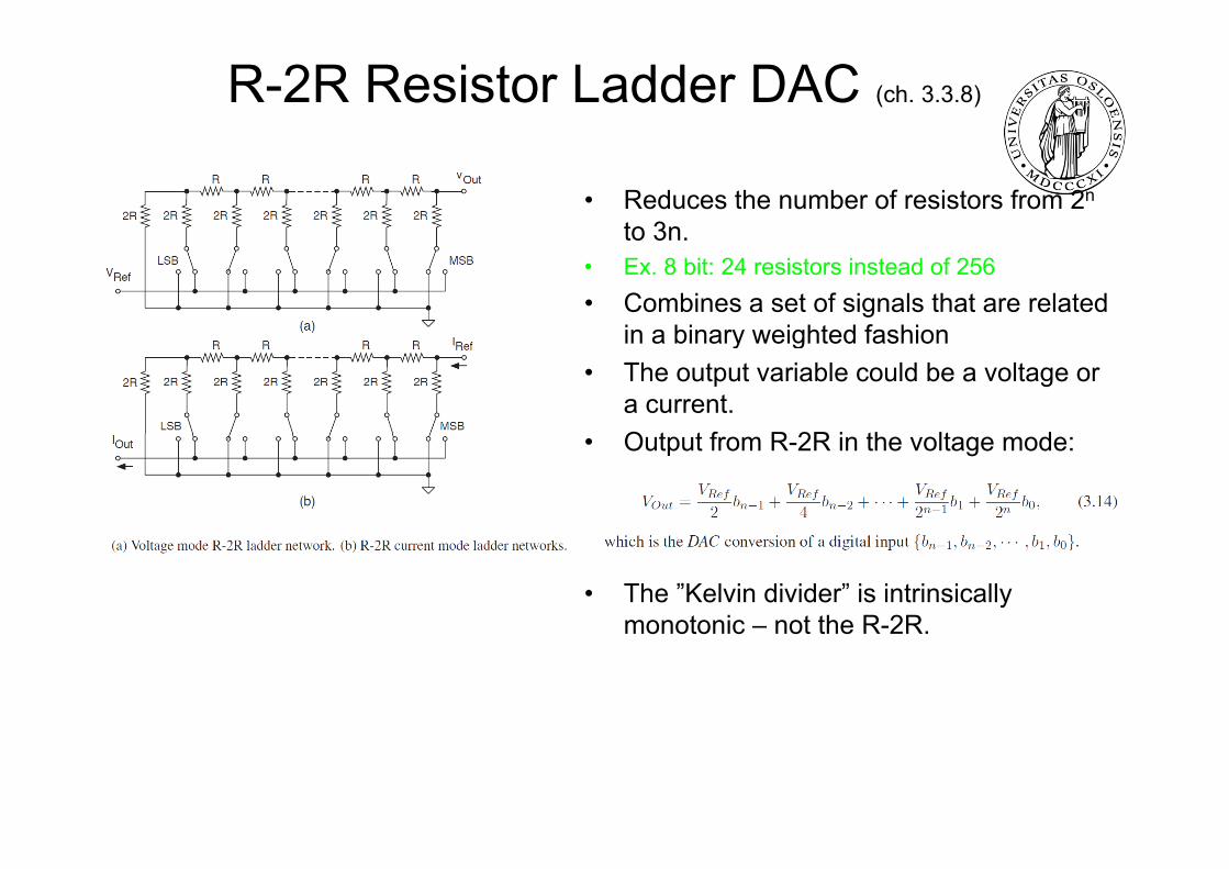
R-2R Resistor Ladder DAC (ch. 3.3.8)
• Reduces the number of resistors from 2n
to 3nto 3n.• Ex. 8 bit: 24 resistors instead of 256• Combines a set of signals that are related
in a binary weighted fashionin a binary weighted fashion• The output variable could be a voltage or
a current.O t t f R 2R i th lt d• Output from R-2R in the voltage mode:
• The ”Kelvin divider” is intrinsicallymonotonic – not the R-2R.monotonic not the R 2R.
R-2R Resistor Ladder DAC
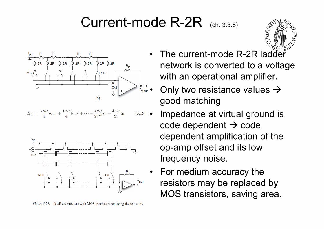
Current-mode R-2R (ch. 3.3.8)
• The current-mode R-2R ladder t k i t d t ltnetwork is converted to a voltage
with an operational amplifier.• Only two resistance values• Only two resistance values
good matching• Impedance at virtual ground is• Impedance at virtual ground is
code dependent codedependent amplification of thep pop-amp offset and its lowfrequency noise.
• For medium accuracy theresistors may be replaced by MOS transistors saving areaMOS transistors, saving area.
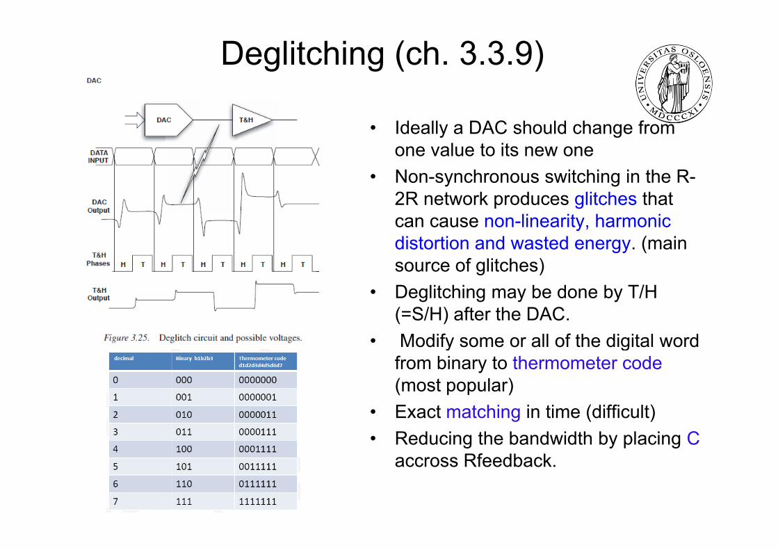
Deglitching (ch. 3.3.9)
• Ideally a DAC should change from one value to its new oneone value to its new one
• Non-synchronous switching in the R-2R network produces glitches thatcan cause non-linearity, harmonicdistortion and wasted energy. (mainsource of glitches)g )
• Deglitching may be done by T/H (=S/H) after the DAC.Modify some or all of the digital word• Modify some or all of the digital wordfrom binary to thermometer code(most popular)
• Exact matching in time (difficult)• Reducing the bandwidth by placing C
accross Rfeedbackaccross Rfeedback.
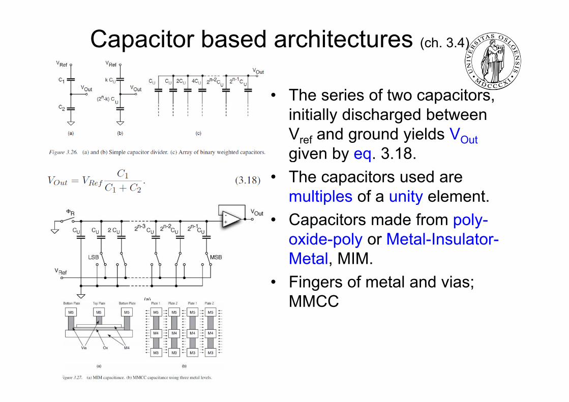
Capacitor based architectures (ch. 3.4)
• The series of two capacitors, i iti ll di h d b tinitially discharged betweenVref and ground yields VOutgiven by eq 3 18given by eq. 3.18.
• The capacitors used aremultiples of a unity element.multiples of a unity element.
• Capacitors made from poly-oxide-poly or Metal-Insulator-p yMetal, MIM.
• Fingers of metal and vias; MMCC
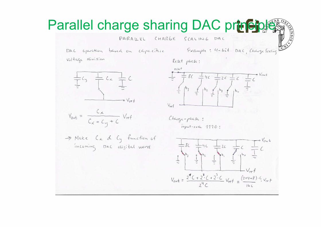
Parallel charge sharing DAC principle

Hybrid Capacitive-Resistive DACs (ch. 3.4.4)
• Resistive and CapacitiveDACs may be combinedto give hybrid solutions.
• Resistive DAC for coarseconversion and capacitivepDAC for the fineconversion.
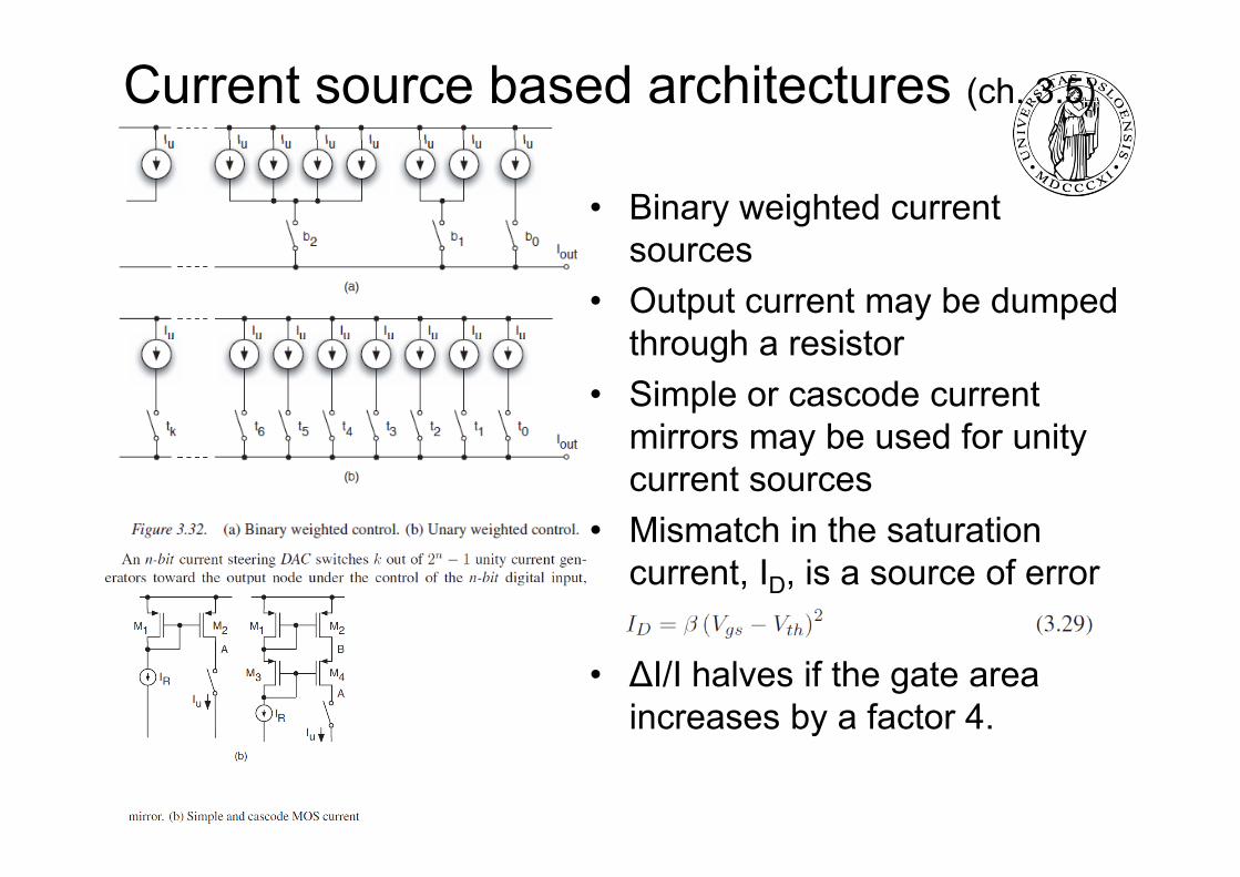
Current source based architectures (ch. 3.5)
• Binary weighted currentsources
• Output current may be dumpedthrough a resistorthrough a resistor
• Simple or cascode currentmirrors may be used for unitymirrors may be used for unitycurrent sources
• Mismatch in the saturationMismatch in the saturationcurrent, ID, is a source of error
• ΔI/I halves if the gate area increases by a factor 4.

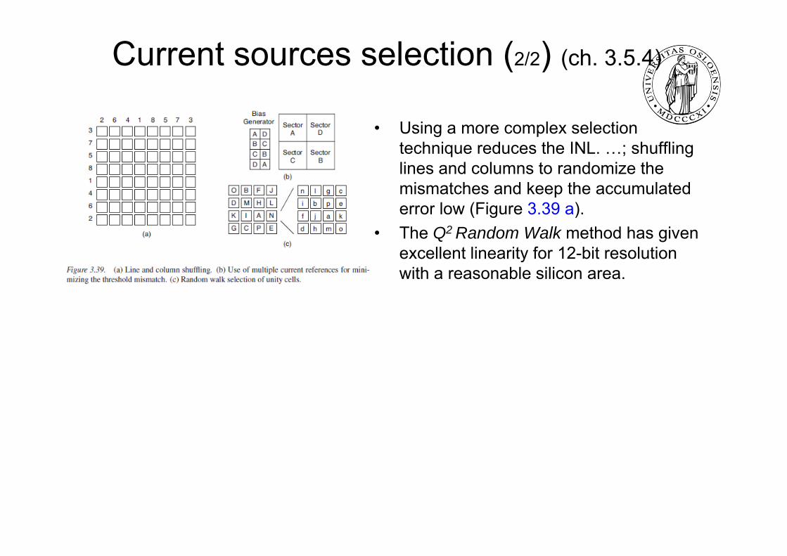
Current sources selection (1/2) (ch. 3.5.4)
• The unity current sources are oftenarranged in a two-dimensional arrayarranged in a two dimensional arraywhose optimum shape is a square with2n/2 lines and columns if the number ofbits n is even.
• The simplest thermometric selection is sequential by lines and columns starting from one corner of the array. Fig 3.38from one corner of the array. Fig 3.38 shows the block diag. Of a possible 8-bit DAC with 70 selected cells correspondingto the input code 01000110. A possiblep pgrading error in x and y directions causesINL.
• Using a more complex selectionUs g a o e co p e se ec otechnique reduces the INL. …
Current sources selection (2/2) (ch. 3.5.4)
• Using a more complex selectiontechnique reduces the INL ; shufflingtechnique reduces the INL. …; shufflinglines and columns to randomize themismatches and keep the accumulatederror low (Figure 3.39 a).( g )
• The Q2 Random Walk method has given excellent linearity for 12-bit resolutionwith a reasonable silicon area.with a reasonable silicon area.
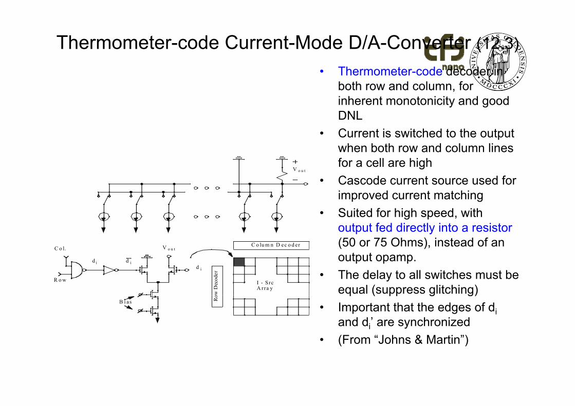
Thermometer-code Current-Mode D/A-Converter (12.3)• Thermometer-code decoder in
both row and column, for inherent monotonicity and good DNLDNL
• Current is switched to the output when both row and column lines for a cell are high
• Cascode current source used for improved current matching
V o u t
• Suited for high speed, with output fed directly into a resistor (50 or 75 Ohms), instead of an C o lu m n D ec o d er
C o l V o u t
output opamp.• The delay to all switches must be
equal (suppress glitching)I - SrcA rra y
ow D
ecod
er
R o w
C o l. V o u t
d i
d id i
q ( pp g g)• Important that the edges of di
and di’ are synchronized• (From “Johns & Martin”)
Ro
B i as
(From Johns & Martin )
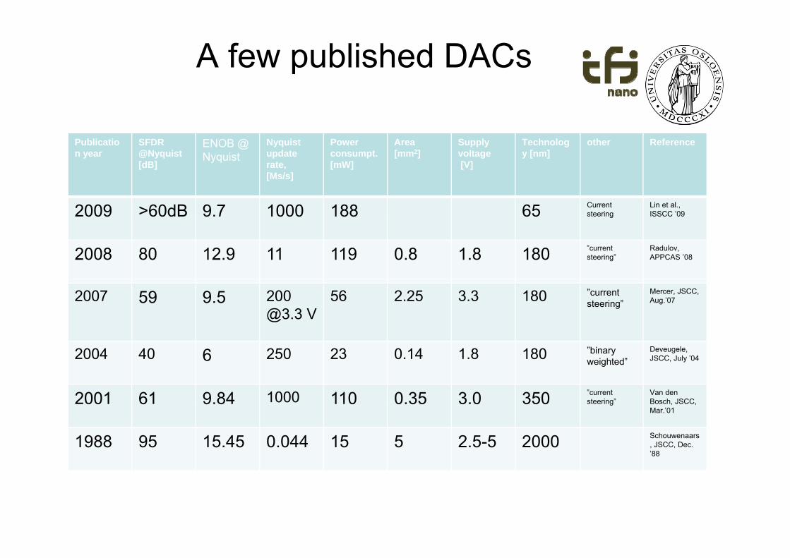
A few published DACs
Publication year
SFDR@Nyquist
ENOB @ Nyquistupdate
Power consumpt
Area[mm2]
Supplyvoltage
Technology [nm]
other Referencen year @Nyquist
[dB]Nyquist update
rate,[Ms/s]
consumpt.[mW]
[mm2] voltage[V]
y [nm]
2009 >60dB 9.7 1000 188 65 Currentsteering
Lin et al., ISSCC ’092009 60dB 9.7 1000 188 65 steering ISSCC 09
2008 80 12.9 11 119 0.8 1.8 180 ”currentsteering”
Radulov, APPCAS ’08
2007 59 9.5 200 @3.3 V
56 2.25 3.3 180 ”currentsteering”
Mercer, JSCC, Aug.’07
2004 40 6 250 23 0.14 1.8 180 ”binaryweighted”
Deveugele, JSCC, July ’04
2001 61 9.84 1000 110 0.35 3.0 350 ”currentsteering”
Van den Bosch, JSCC, Mar.’01
1988 95 15.45 0.044 15 5 2.5-5 2000 Schouwenaars, JSCC, Dec. ’88
Litterature• Johns & Martin: ”Analog Integrated Circuit Design”• Franco Maloberti: ”Data Converters”
30

Next week, 1/3:
• More on Nyquist Analog to Digital Converters (ch. 4 in ”Maloberti”Maloberti
• Messages are given on the INF4420 homepage.g g p g
• Questions: [email protected] , 22852703 / 90013264 Q @ , 3 3