Embed Size (px)
Citation preview
Department of Electrical and Computer Engineering
Vishal Saxena -1-
Pipelined Analog-to-Digital
Converters
Vishal Saxena, Boise State University ([email protected])
Vishal Saxena -2-
Multi-Step A/D Conversion Basics
2
Vishal Saxena -3-
Motivation for Multi-Step Converters
Flash A/D Converters
Area and power consumption increase exponentially with
number of bits N
Impractical beyond 7-8 bits
Multi-step conversion-Coarse conversion followed by fine
conversion
Multi-step converters
Subranging converters
Multi step conversion takes more time
Pipelining to increase sampling rate
Objective: Understand digital redundancy concept in multi-step converters
Vishal Saxena -4-
Two-step A/D Converter - Basic Operation
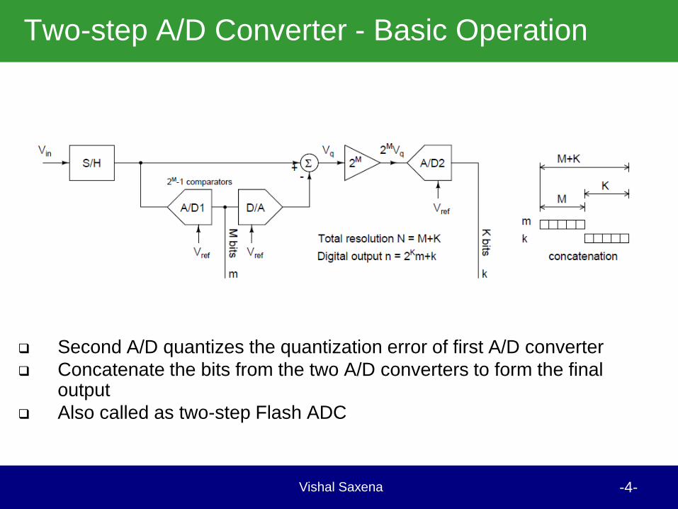
Second A/D quantizes the quantization error of first A/D converter
Concatenate the bits from the two A/D converters to form the final output
Also called as two-step Flash ADC
Vishal Saxena -5-
Two-step A/D Converter - Basic Operation
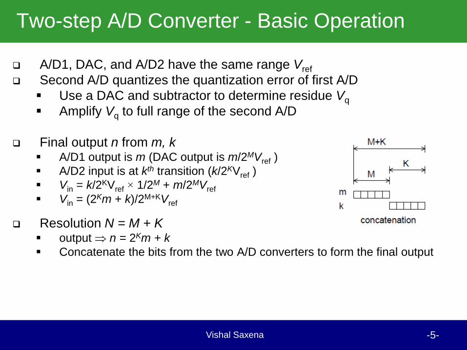
A/D1, DAC, and A/D2 have the same range Vref
Second A/D quantizes the quantization error of first A/D
Use a DAC and subtractor to determine residue Vq
Amplify Vq to full range of the second A/D
Final output n from m, k A/D1 output is m (DAC output is m/2MVref )
A/D2 input is at kth transition (k/2KVref )
Vin = k/2KVref × 1/2M + m/2MVref
Vin = (2Km + k)/2M+KVref
Resolution N = M + K output n = 2Km + k
Concatenate the bits from the two A/D converters to form the final output
Vishal Saxena -6-
Two-step A/D Converter – Example with M=3, K=2
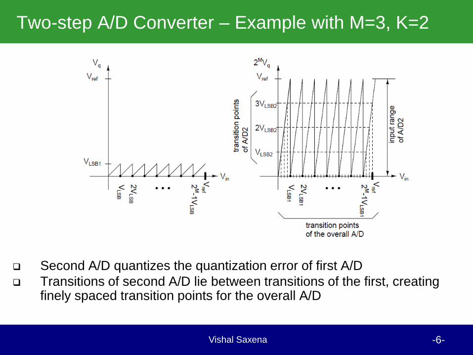
Second A/D quantizes the quantization error of first A/D
Transitions of second A/D lie between transitions of the first, creating finely spaced transition points for the overall A/D
Vishal Saxena -7-
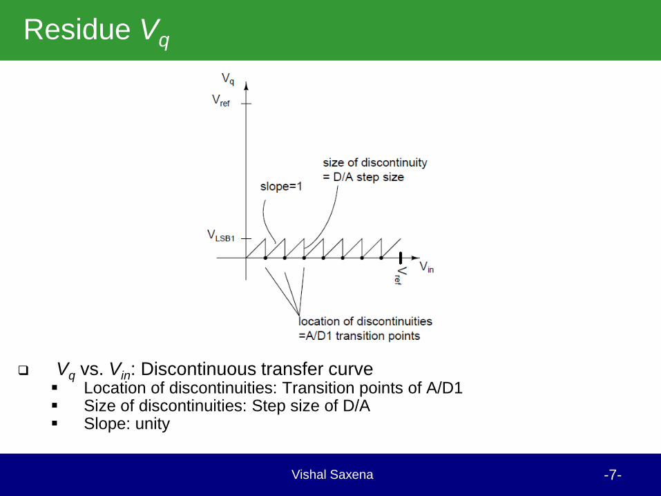
Residue Vq
Vq vs. Vin: Discontinuous transfer curve Location of discontinuities: Transition points of A/D1 Size of discontinuities: Step size of D/A Slope: unity
Vishal Saxena -8-
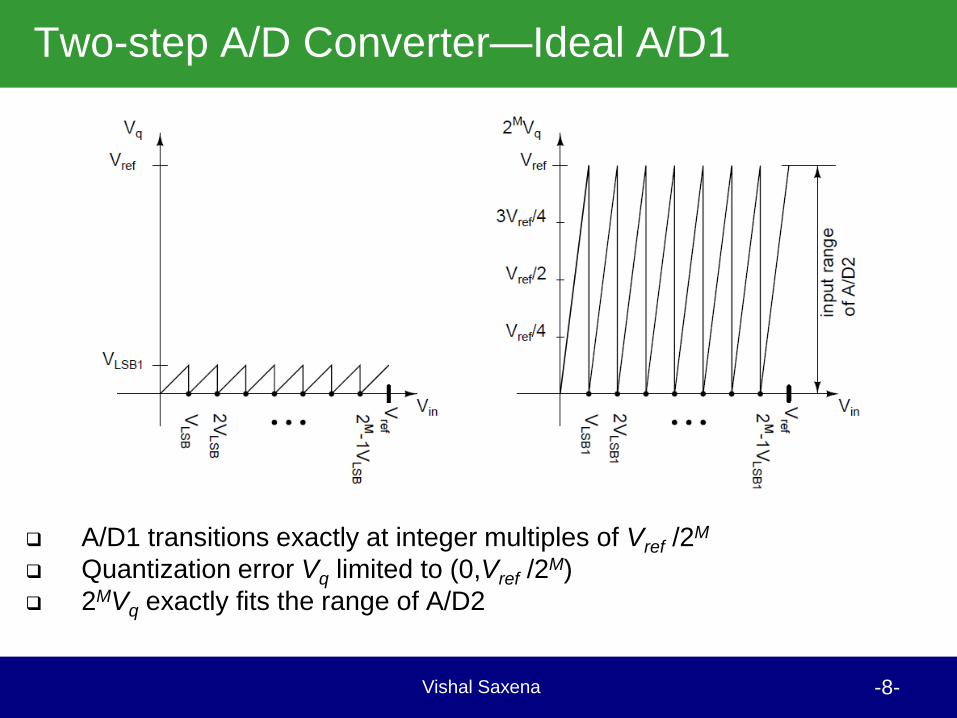
Two-step A/D Converter—Ideal A/D1
A/D1 transitions exactly at integer multiples of Vref /2M
Quantization error Vq limited to (0,Vref /2M)
2MVq exactly fits the range of A/D2
Vishal Saxena -9-
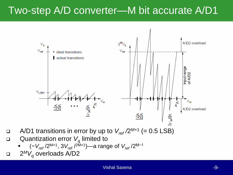
Two-step A/D converter—M bit accurate A/D1
A/D1 transitions in error by up to Vref /2M+1 (= 0.5 LSB)
Quantization error Vq limited to (−Vref /2
M+1, 3Vref /2M+1)—a range of Vref /2
M−1
2MVq overloads A/D2
Vishal Saxena -10-
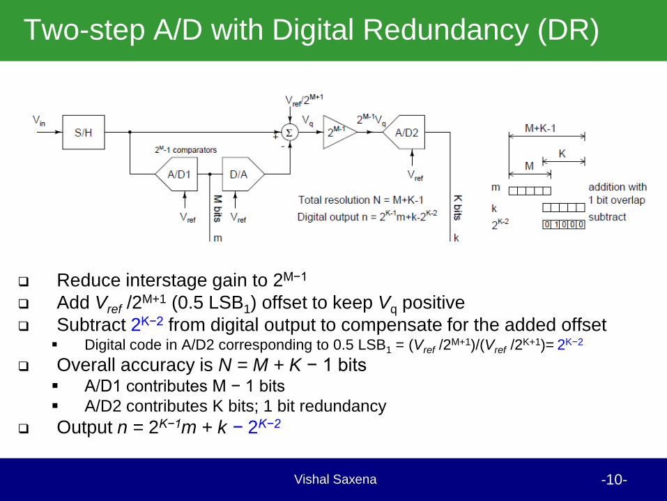
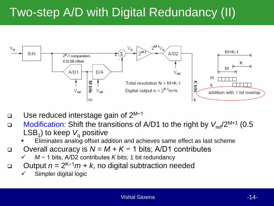
Two-step A/D with Digital Redundancy (DR)
Reduce interstage gain to 2M−1
Add Vref /2M+1 (0.5 LSB1) offset to keep Vq positive
Subtract 2K−2 from digital output to compensate for the added offset Digital code in A/D2 corresponding to 0.5 LSB1 = (Vref /2
M+1)/(Vref /2K+1)= 2K−2
Overall accuracy is N = M + K − 1 bits A/D1 contributes M − 1 bits
A/D2 contributes K bits; 1 bit redundancy
Output n = 2K−1m + k − 2K−2
Vishal Saxena -11-
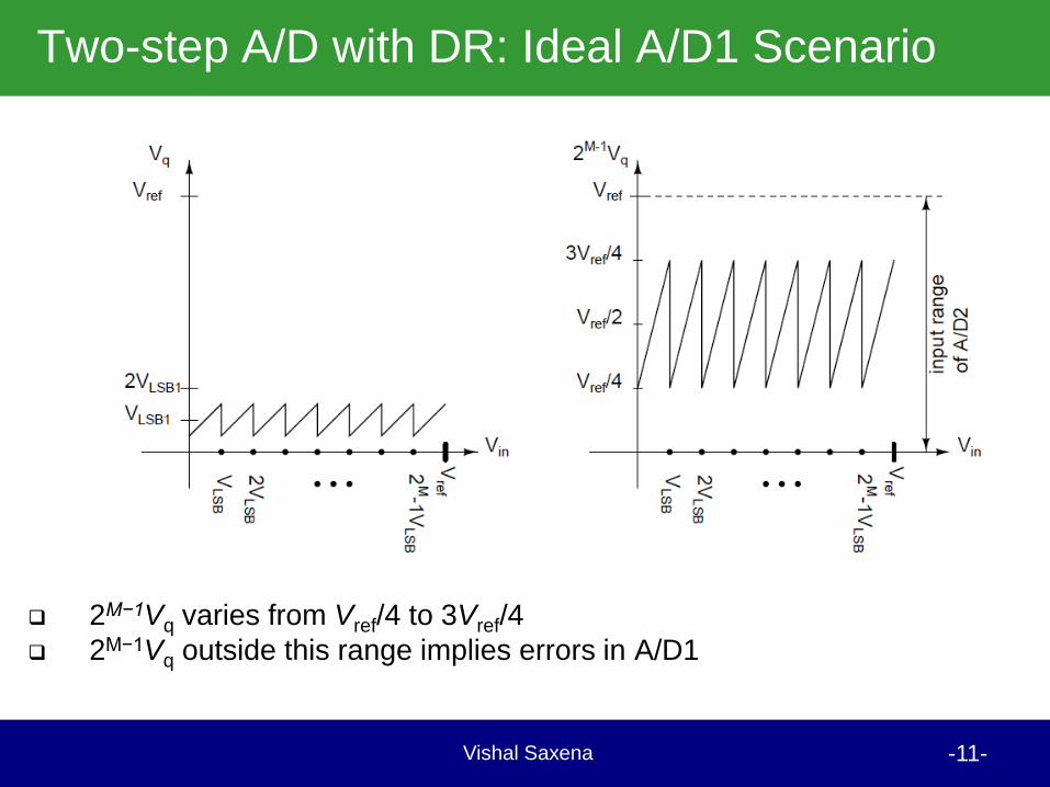
Two-step A/D with DR: Ideal A/D1 Scenario
2M−1Vq varies from Vref/4 to 3Vref/4
2M−1Vq outside this range implies errors in A/D1
Vishal Saxena -12-
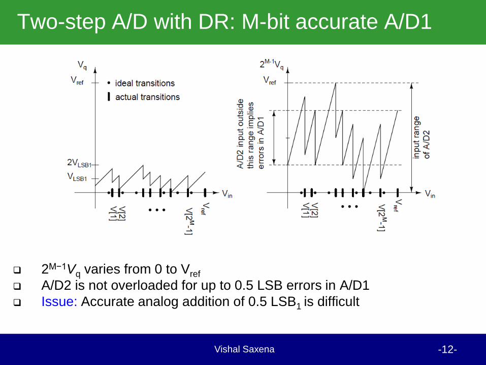
Two-step A/D with DR: M-bit accurate A/D1
2M−1Vq varies from 0 to Vref
A/D2 is not overloaded for up to 0.5 LSB errors in A/D1
Issue: Accurate analog addition of 0.5 LSB1 is difficult
Vishal Saxena -13-
Two-step A/D with DR: M-bit accurate A/D1
Recall that output n = 2K−1m + k − 2K−2
A/D1 Transition shifted to the left
m greater than its ideal value by 1
k lesser than its ideal value by 2K−1
A/D output n = 2K−1m + k − 2K−2 doesn’t change
A/D1 Transition shifted to the right m lesser than its ideal value by 1
k greater than its ideal value by 2K−1
A/D output n = 2K−1m + k − 2K−2 doesn’t change
1 LSB error in m can be corrected
Vishal Saxena -14-
Two-step A/D with Digital Redundancy (II)
Use reduced interstage gain of 2M−1
Modification: Shift the transitions of A/D1 to the right by Vref/2M+1 (0.5
LSB1) to keep Vq positive Eliminates analog offset addition and achieves same effect as last scheme
Overall accuracy is N = M + K − 1 bits; A/D1 contributes M − 1 bits, A/D2 contributes K bits; 1 bit redundancy
Output n = 2K−1m + k, no digital subtraction needed Simpler digital logic
Vishal Saxena -15-
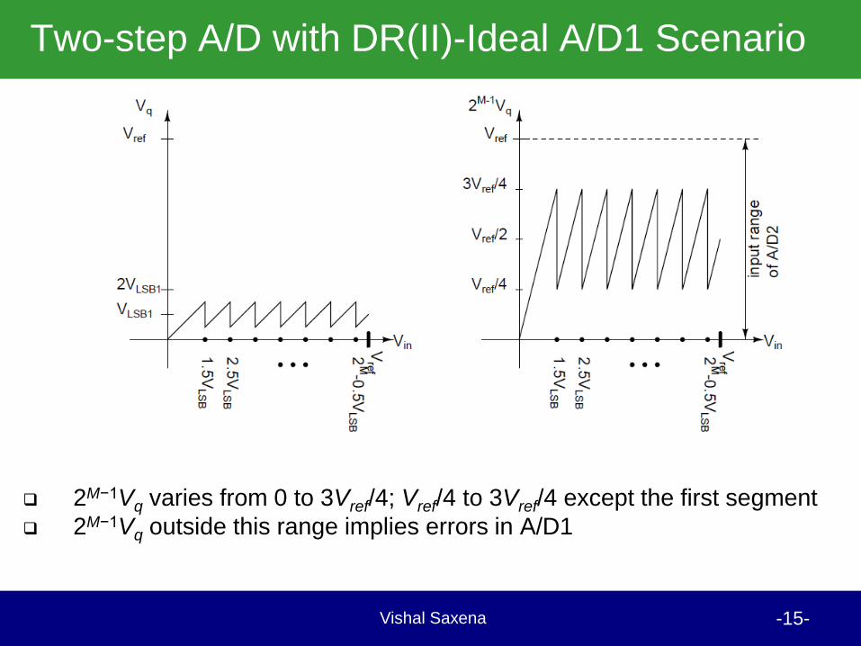
Two-step A/D with DR(II)-Ideal A/D1 Scenario
2M−1Vq varies from 0 to 3Vref/4; Vref/4 to 3Vref/4 except the first segment
2M−1Vq outside this range implies errors in A/D1
Vishal Saxena -16-
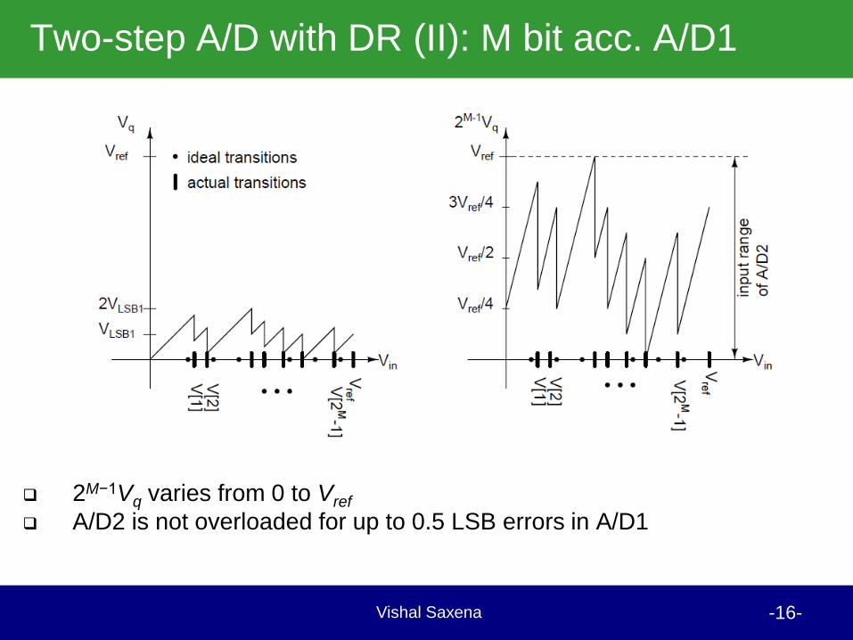
Two-step A/D with DR (II): M bit acc. A/D1
2M−1Vq varies from 0 to Vref
A/D2 is not overloaded for up to 0.5 LSB errors in A/D1
Vishal Saxena -17-
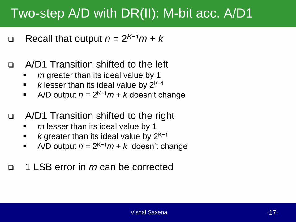
Two-step A/D with DR(II): M-bit acc. A/D1
Recall that output n = 2K−1m + k
A/D1 Transition shifted to the left
m greater than its ideal value by 1
k lesser than its ideal value by 2K−1
A/D output n = 2K−1m + k doesn’t change
A/D1 Transition shifted to the right m lesser than its ideal value by 1
k greater than its ideal value by 2K−1
A/D output n = 2K−1m + k doesn’t change
1 LSB error in m can be corrected
Vishal Saxena -18-
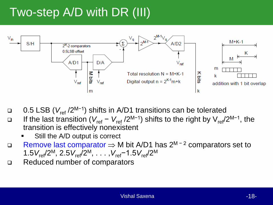
Two-step A/D with DR (III)
0.5 LSB (Vref /2M−1) shifts in A/D1 transitions can be tolerated
If the last transition (Vref − Vref /2M−1) shifts to the right by Vref/2
M−1, the transition is effectively nonexistent Still the A/D output is correct
Remove last comparator M bit A/D1 has 2M − 2 comparators set to 1.5Vref/2
M, 2.5Vref/2M, . . . ,Vref−1.5Vref/2
M
Reduced number of comparators
Vishal Saxena -19-
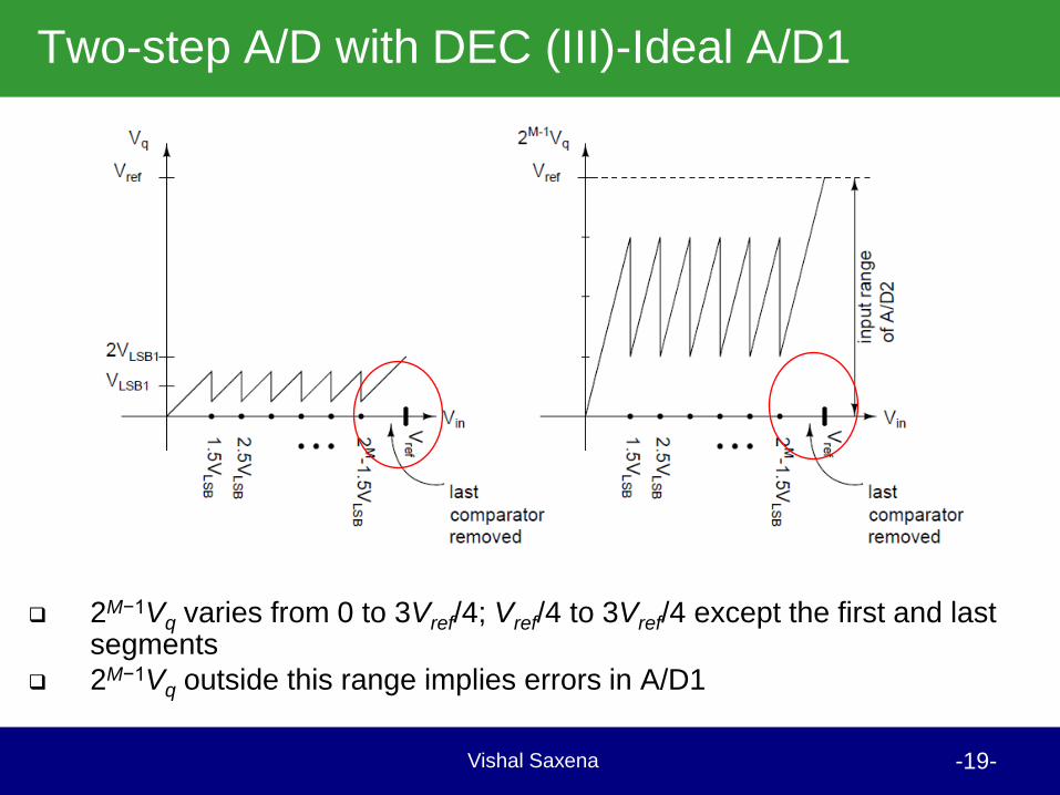
Two-step A/D with DEC (III)-Ideal A/D1
2M−1Vq varies from 0 to 3Vref/4; Vref/4 to 3Vref/4 except the first and last segments
2M−1Vq outside this range implies errors in A/D1
Vishal Saxena -20-
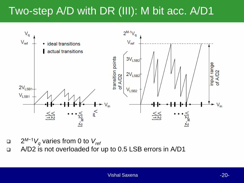
Two-step A/D with DR (III): M bit acc. A/D1
2M−1Vq varies from 0 to Vref
A/D2 is not overloaded for up to 0.5 LSB errors in A/D1
Vishal Saxena -21-
Two-step A/D with DR(III): M-bit acc. A/D1
Recall that output n = 2K−1m + k
A/D1 Transition shifted to the left
m greater than its ideal value by 1
k lesser than its ideal value by 2K−1
A/D output n = 2K−1m + k doesn’t change
A/D1 Transition shifted to the right m lesser than its ideal value by 1
k greater than its ideal value by 2K−1
A/D output n = 2K−1m + k doesn’t change
1 LSB error in m can be corrected
Vishal Saxena -22-
Multi-step Converters
Two-step architecture can be extended to multiple steps
All stages except the last have their outputs digitally corrected from the following A/D output
Number of effective bits in each stage is one less than the stage A/D resolution
Accuracy of components in each stage depends on the accuracy of the A/D converter following it
Accuracy requirements less stringent down the pipeline, but optimizing every stage separately increases design effort
Pipelined operation to obtain high sampling rates
Last stage is not digitally corrected
Vishal Saxena -23-
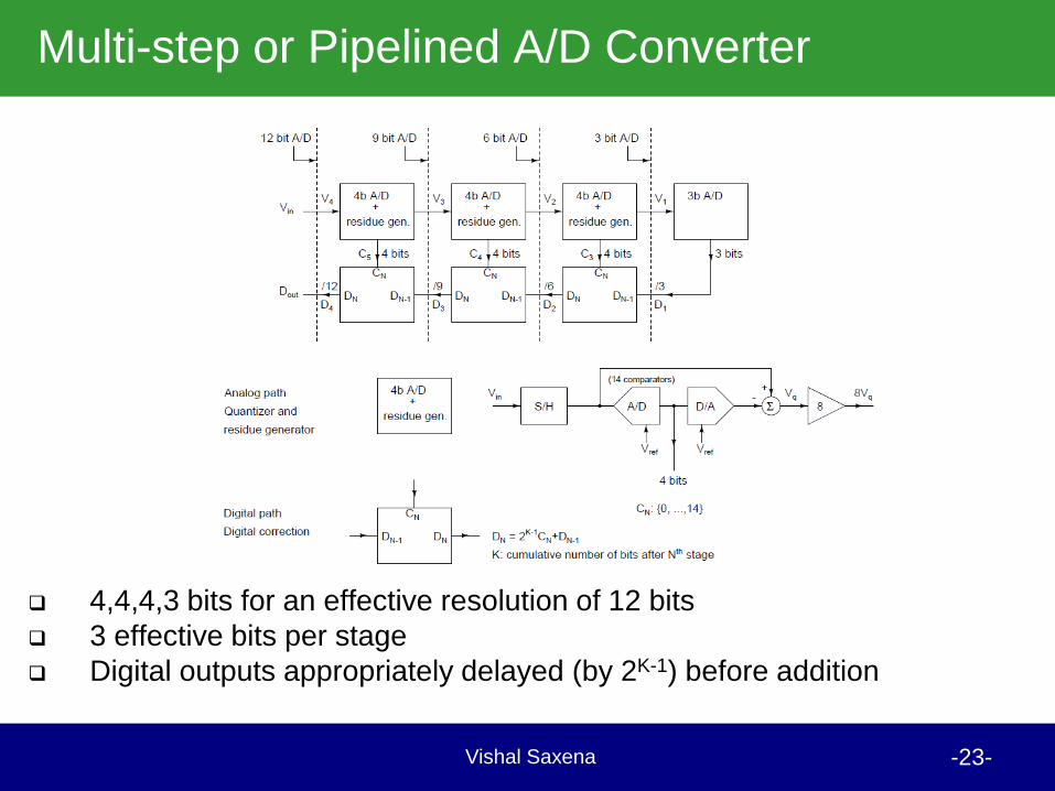
Multi-step or Pipelined A/D Converter
4,4,4,3 bits for an effective resolution of 12 bits
3 effective bits per stage
Digital outputs appropriately delayed (by 2K-1) before addition
Vishal Saxena -24-
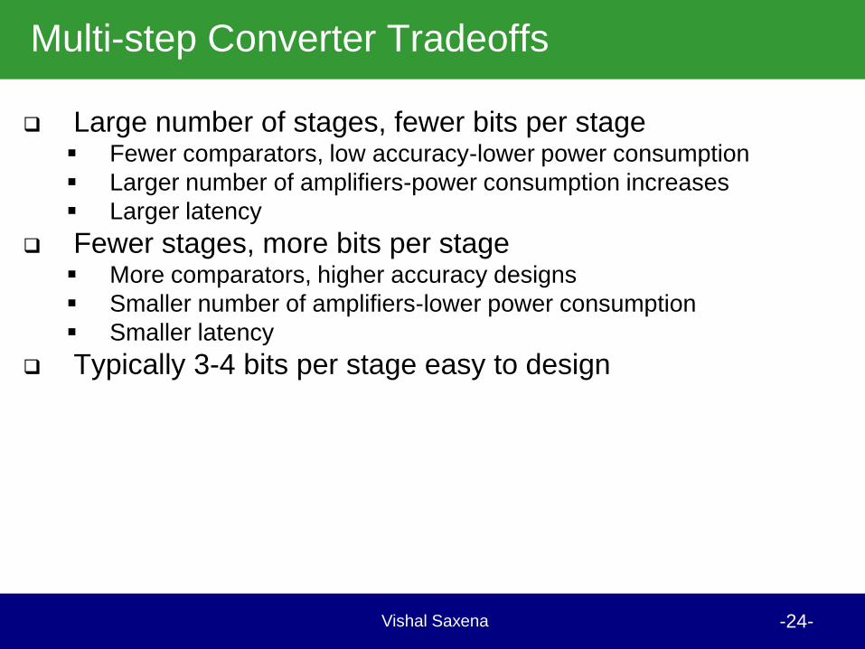
Multi-step Converter Tradeoffs
Large number of stages, fewer bits per stage Fewer comparators, low accuracy-lower power consumption
Larger number of amplifiers-power consumption increases
Larger latency
Fewer stages, more bits per stage More comparators, higher accuracy designs
Smaller number of amplifiers-lower power consumption
Smaller latency
Typically 3-4 bits per stage easy to design
Vishal Saxena -25-
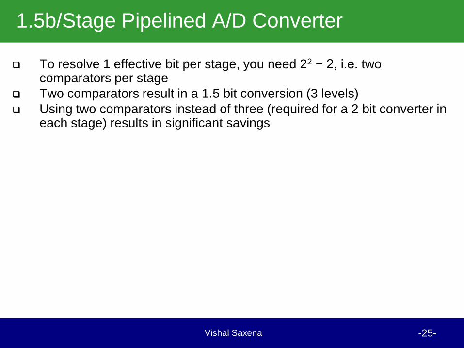
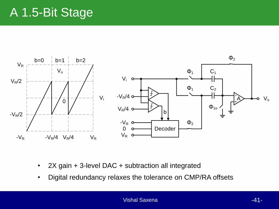
1.5b/Stage Pipelined A/D Converter
To resolve 1 effective bit per stage, you need 22 − 2, i.e. two comparators per stage
Two comparators result in a 1.5 bit conversion (3 levels)
Using two comparators instead of three (required for a 2 bit converter in each stage) results in significant savings
Vishal Saxena -26-
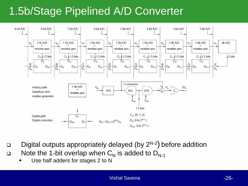
1.5b/Stage Pipelined A/D Converter
Digital outputs appropriately delayed (by 2N-2) before addition
Note the 1-bit overlap when CN is added to DN-1 Use half adders for stages 2 to N
Vishal Saxena -27-
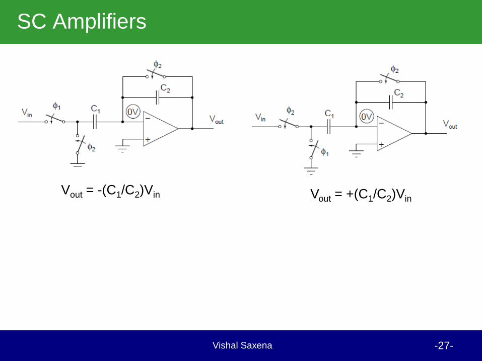
SC Amplifiers
Vout = -(C1/C2)Vin Vout = +(C1/C2)Vin
Vishal Saxena -28-
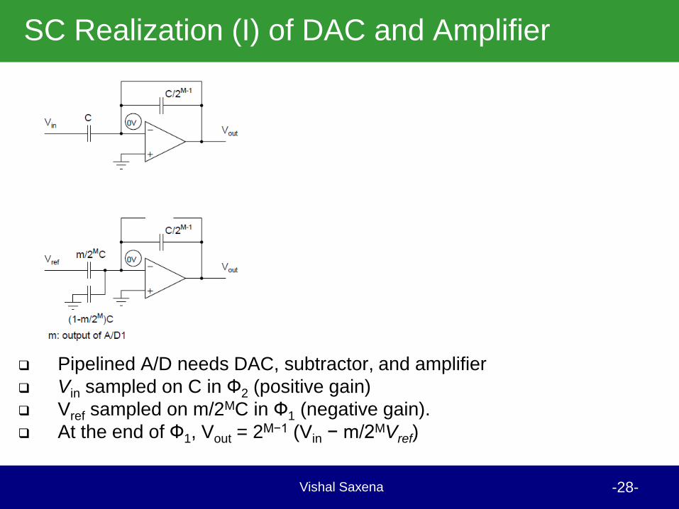
SC Realization (I) of DAC and Amplifier
Pipelined A/D needs DAC, subtractor, and amplifier
Vin sampled on C in Ф2 (positive gain)
Vref sampled on m/2MC in Ф1 (negative gain).
At the end of Ф1, Vout = 2M−1 (Vin − m/2MVref)
Vishal Saxena -29-
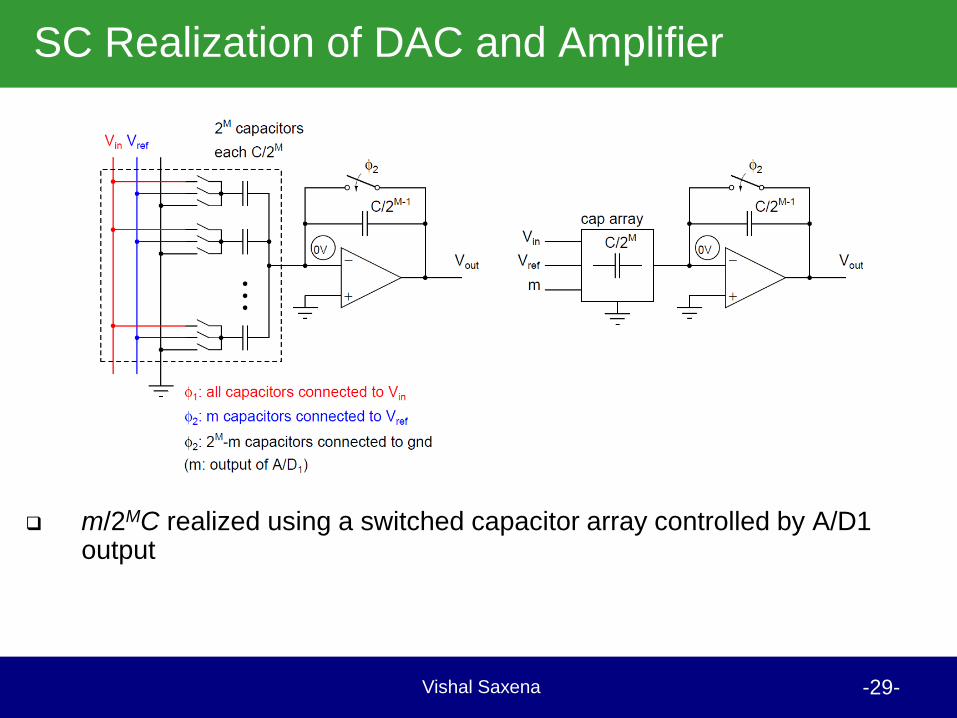
SC Realization of DAC and Amplifier
m/2MC realized using a switched capacitor array controlled by A/D1 output
Vishal Saxena -30-
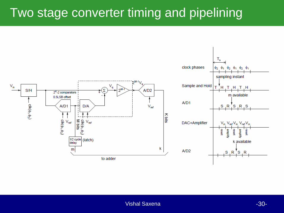
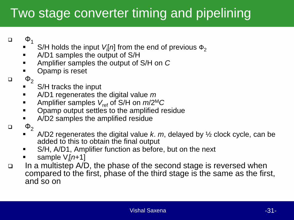
Two stage converter timing and pipelining
Vishal Saxena -31-
Two stage converter timing and pipelining
Ф1 S/H holds the input Vi[n] from the end of previous Ф2
A/D1 samples the output of S/H Amplifier samples the output of S/H on C Opamp is reset
Ф2 S/H tracks the input A/D1 regenerates the digital value m Amplifier samples Vref of S/H on m/2MC Opamp output settles to the amplified residue A/D2 samples the amplified residue
Ф2 A/D2 regenerates the digital value k. m, delayed by ½ clock cycle, can be
added to this to obtain the final output S/H, A/D1, Amplifier function as before, but on the next sample Vi[n+1]
In a multistep A/D, the phase of the second stage is reversed when compared to the first, phase of the third stage is the same as the first, and so on
Vishal Saxena -32-
Pipelined A/D Implementation
Vishal Saxena -33-
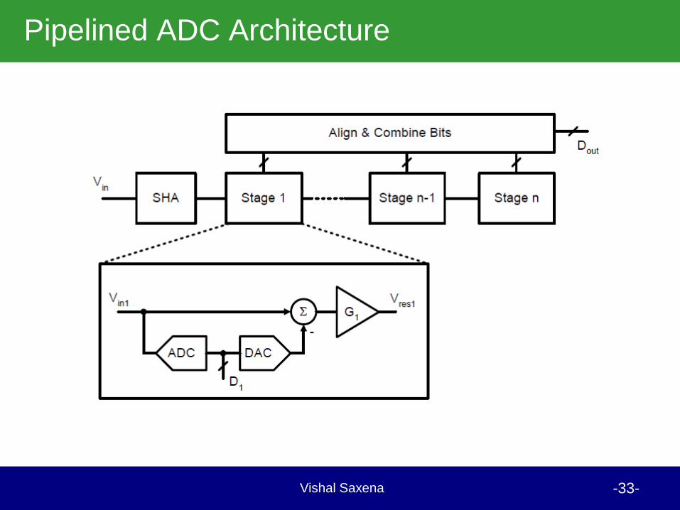
Pipelined ADC Architecture
Vishal Saxena -34-
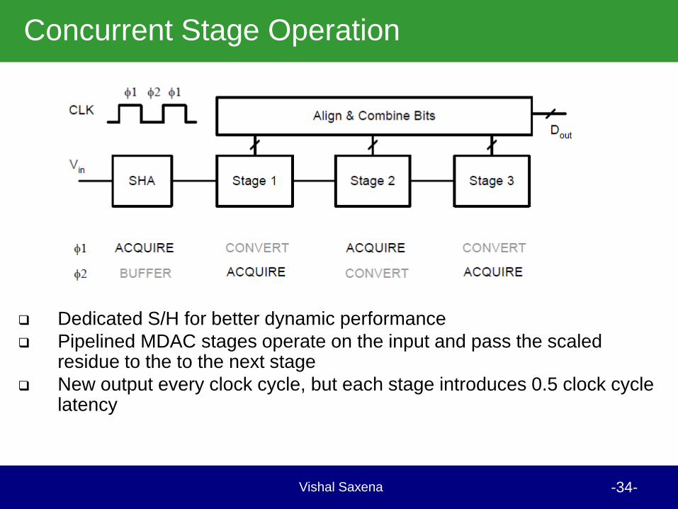
Concurrent Stage Operation
Dedicated S/H for better dynamic performance
Pipelined MDAC stages operate on the input and pass the scaled residue to the to the next stage
New output every clock cycle, but each stage introduces 0.5 clock cycle latency
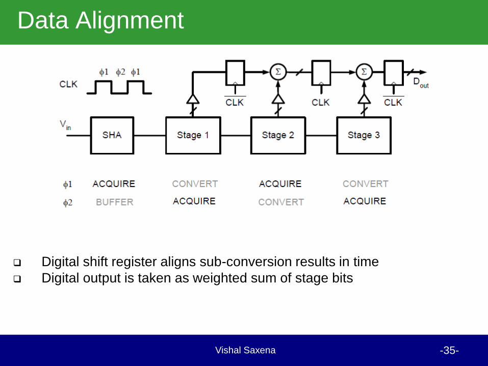
Vishal Saxena -35-
Data Alignment
Digital shift register aligns sub-conversion results in time
Digital output is taken as weighted sum of stage bits
Vishal Saxena -36-
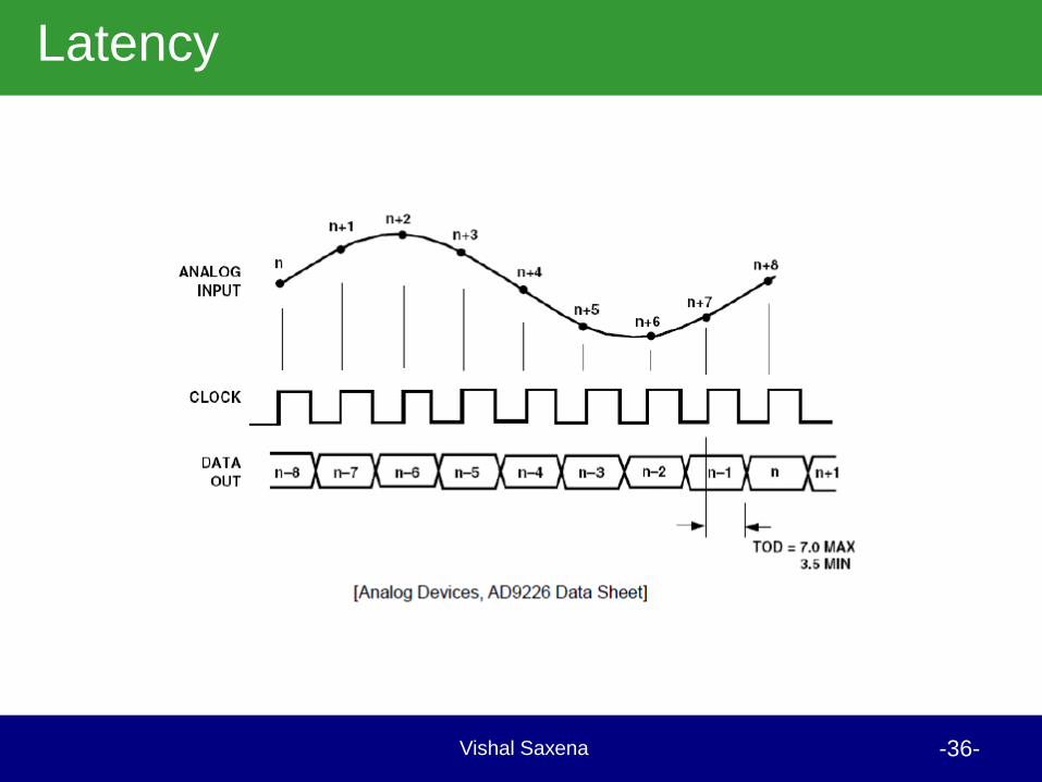
Latency
Vishal Saxena -37-
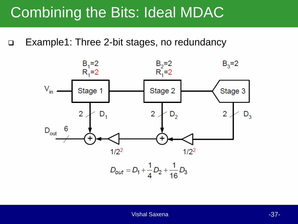
Combining the Bits: Ideal MDAC
Example1: Three 2-bit stages, no redundancy
Vishal Saxena -38-
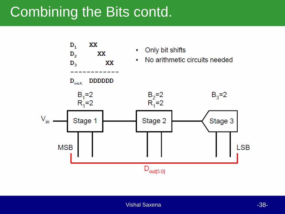
Combining the Bits contd.
Vishal Saxena -39-
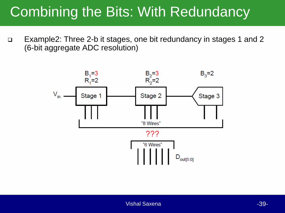
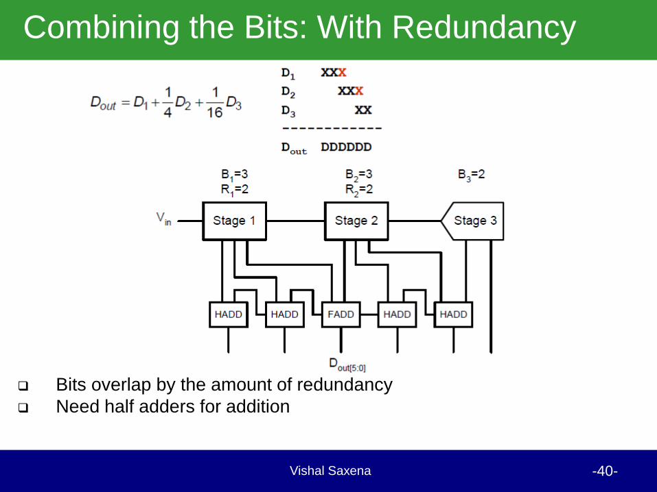
Combining the Bits: With Redundancy
Example2: Three 2-b it stages, one bit redundancy in stages 1 and 2 (6-bit aggregate ADC resolution)
Vishal Saxena -40-
Combining the Bits: With Redundancy
Bits overlap by the amount of redundancy
Need half adders for addition
Vishal Saxena -41-
A 1.5-Bit Stage
• 2X gain + 3-level DAC + subtraction all integrated
• Digital redundancy relaxes the tolerance on CMP/RA offsets
Vo
Vi
0-VR
VR
Decoder
Φ1 C1
Φ1 C2
Φ2
Φ1e
A
Φ2
-VR/4
VR/4b
-VR/4 VR/4
0
VR/2
-VR/2
Vi
-VR
VR
VR
b=0 b=2b=1
Vo
Vishal Saxena -42-
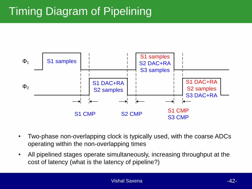
Timing Diagram of Pipelining
S1 samples
S1 DAC+RA
S2 samples
S1 samples
S2 DAC+RA
S3 samples
S1 DAC+RA
S2 samples
S3 DAC+RA
S1 CMP S2 CMPS1 CMP
S3 CMP
Φ1
Φ2
• Two-phase non-overlapping clock is typically used, with the coarse ADCs
operating within the non-overlapping times
• All pipelined stages operate simultaneously, increasing throughput at the
cost of latency (what is the latency of pipeline?)
Vishal Saxena -43-
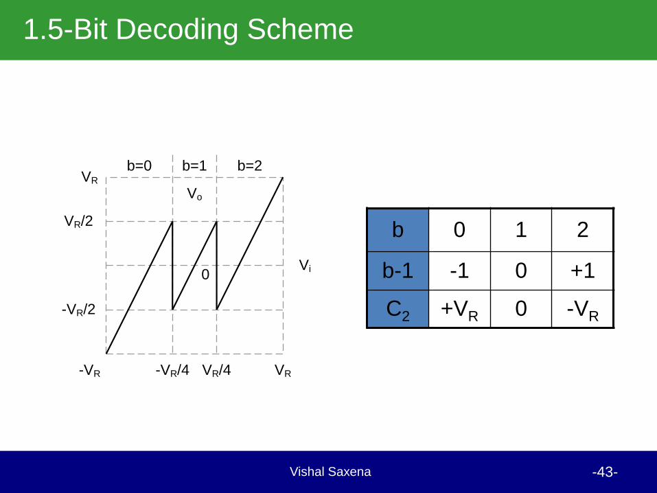
1.5-Bit Decoding Scheme
b 0 1 2
b-1 -1 0 +1
C2 +VR 0 -VR
-VR/4 VR/4
0
VR/2
-VR/2
Vi
-VR
VR
VR
b=0 b=2b=1
Vo
Vishal Saxena -44-
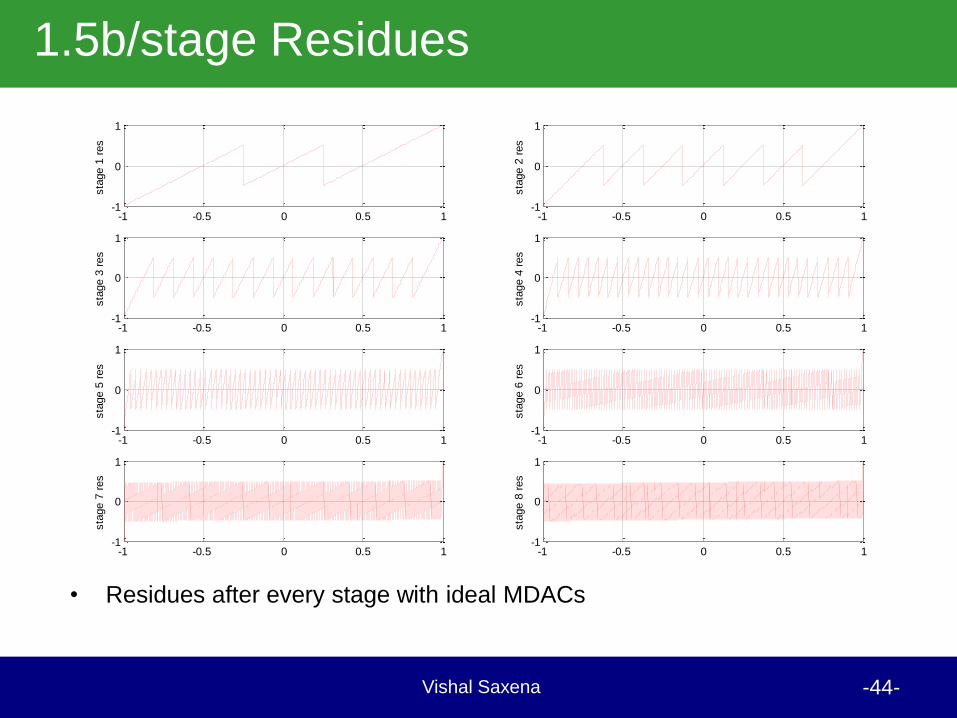
1.5b/stage Residues
-1 -0.5 0 0.5 1-1
0
1
sta
ge 1
res
-1 -0.5 0 0.5 1-1
0
1
sta
ge 2
res
-1 -0.5 0 0.5 1-1
0
1
sta
ge 3
res
-1 -0.5 0 0.5 1-1
0
1
sta
ge 4
res
-1 -0.5 0 0.5 1-1
0
1
sta
ge 5
res
-1 -0.5 0 0.5 1-1
0
1
sta
ge 6
res
-1 -0.5 0 0.5 1-1
0
1
sta
ge 7
res
-1 -0.5 0 0.5 1-1
0
1
sta
ge 8
res
• Residues after every stage with ideal MDACs
Vishal Saxena -45-
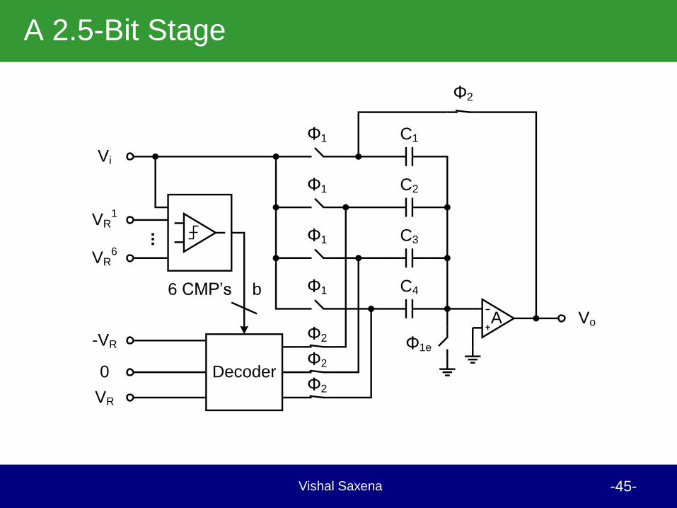
A 2.5-Bit Stage
Vo
Vi
0
-VR
VR
Decoder
Φ1e
A
Φ2
VR6
VR1
6 CMP’s
...
Φ1 C1
Φ1 C2
Φ2
C3
C4
Φ1
Φ1
Φ2
Φ2
b
Vishal Saxena -46-
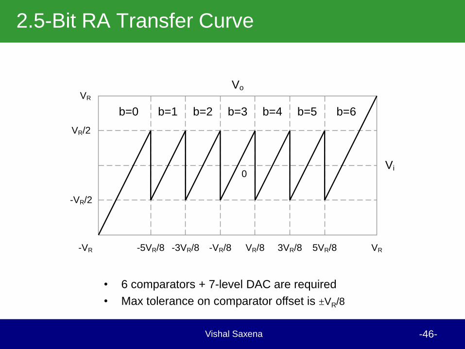
2.5-Bit RA Transfer Curve
• 6 comparators + 7-level DAC are required
• Max tolerance on comparator offset is ±VR/8
b=1 b=3 b=5b=0 b=2 b=4 b=6
Vi
Vo
-5VR/8 VR/8
VR/2
-VR/2
0
-3VR/8 -VR/8 5VR/83VR/8-VR VR
VR
Vishal Saxena -47-
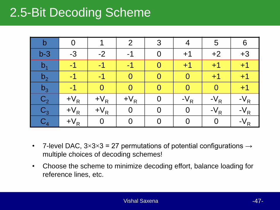
2.5-Bit Decoding Scheme
b 0 1 2 3 4 5 6
b-3 -3 -2 -1 0 +1 +2 +3
b1 -1 -1 -1 0 +1 +1 +1
b2 -1 -1 0 0 0 +1 +1
b3 -1 0 0 0 0 0 +1
C2 +VR +VR +VR 0 -VR -VR -VR
C3 +VR +VR 0 0 0 -VR -VR
C4 +VR 0 0 0 0 0 -VR
• 7-level DAC, 3×3×3 = 27 permutations of potential configurations →
multiple choices of decoding schemes!
• Choose the scheme to minimize decoding effort, balance loading for
reference lines, etc.
Vishal Saxena -48-
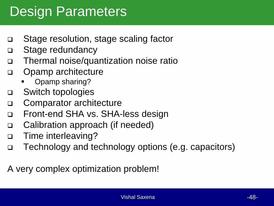
Design Parameters
Stage resolution, stage scaling factor
Stage redundancy
Thermal noise/quantization noise ratio
Opamp architecture Opamp sharing?
Switch topologies
Comparator architecture
Front-end SHA vs. SHA-less design
Calibration approach (if needed)
Time interleaving?
Technology and technology options (e.g. capacitors)
A very complex optimization problem!
Vishal Saxena -49-
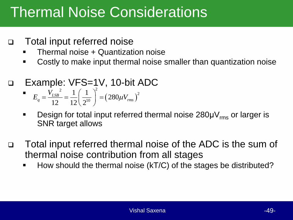
Thermal Noise Considerations
Total input referred noise Thermal noise + Quantization noise
Costly to make input thermal noise smaller than quantization noise
Example: VFS=1V, 10-bit ADC
Design for total input referred thermal noise 280μVrms or larger is
SNR target allows
Total input referred thermal noise of the ADC is the sum of thermal noise contribution from all stages How should the thermal noise (kT/C) of the stages be distributed?
22
2
10
1 1280
12 12 2
LSBq rms
VE V
Vishal Saxena -50-
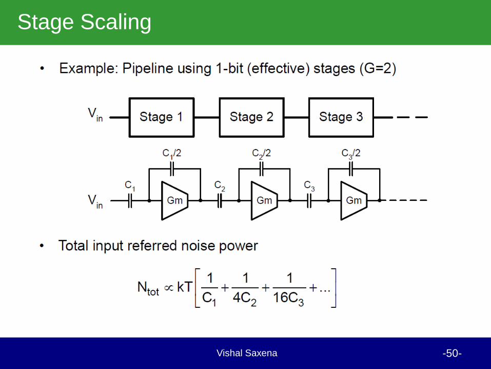
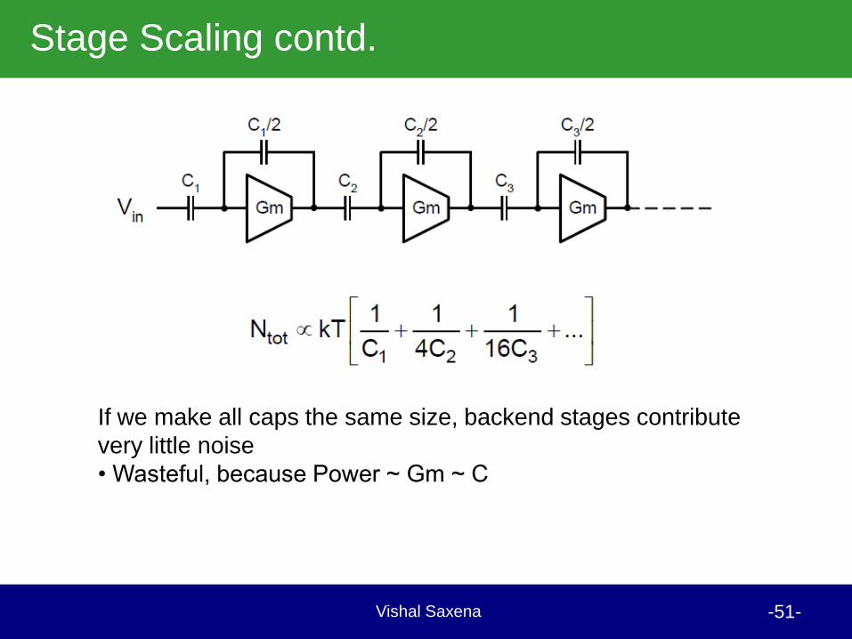
Stage Scaling
Vishal Saxena -51-
Stage Scaling contd.
If we make all caps the same size, backend stages contribute
very little noise
• Wasteful, because Power ~ Gm ~ C
Vishal Saxena -52-
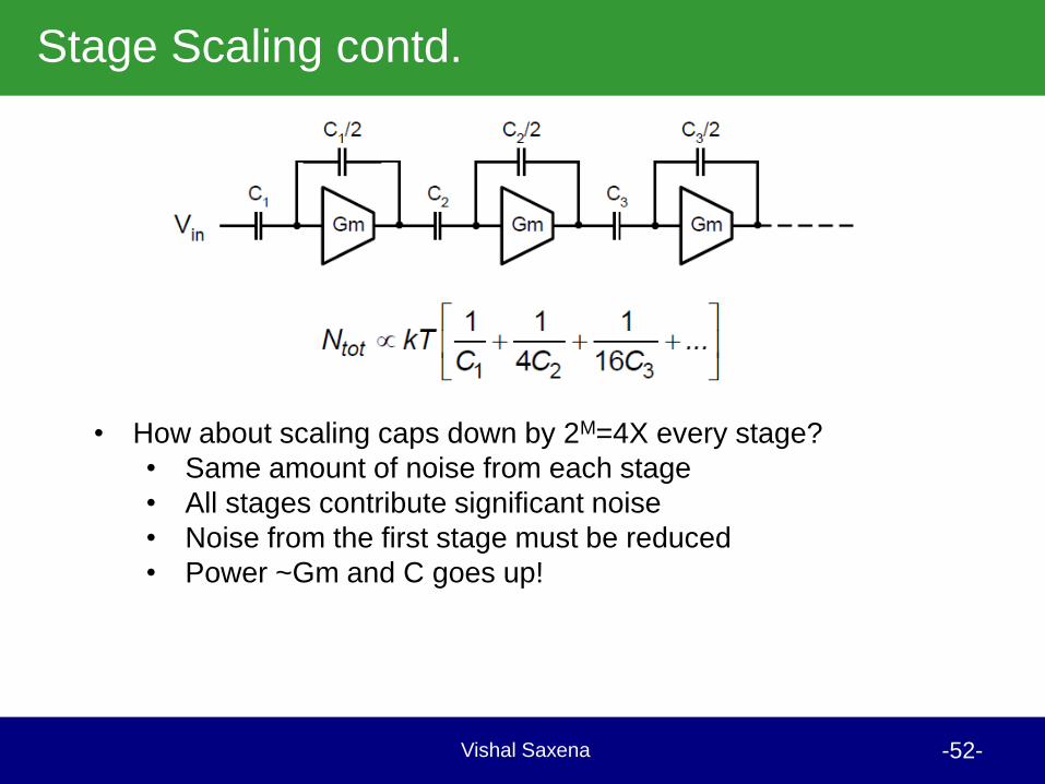
Stage Scaling contd.
• How about scaling caps down by 2M=4X every stage?
• Same amount of noise from each stage
• All stages contribute significant noise
• Noise from the first stage must be reduced
• Power ~Gm and C goes up!
Vishal Saxena -53-
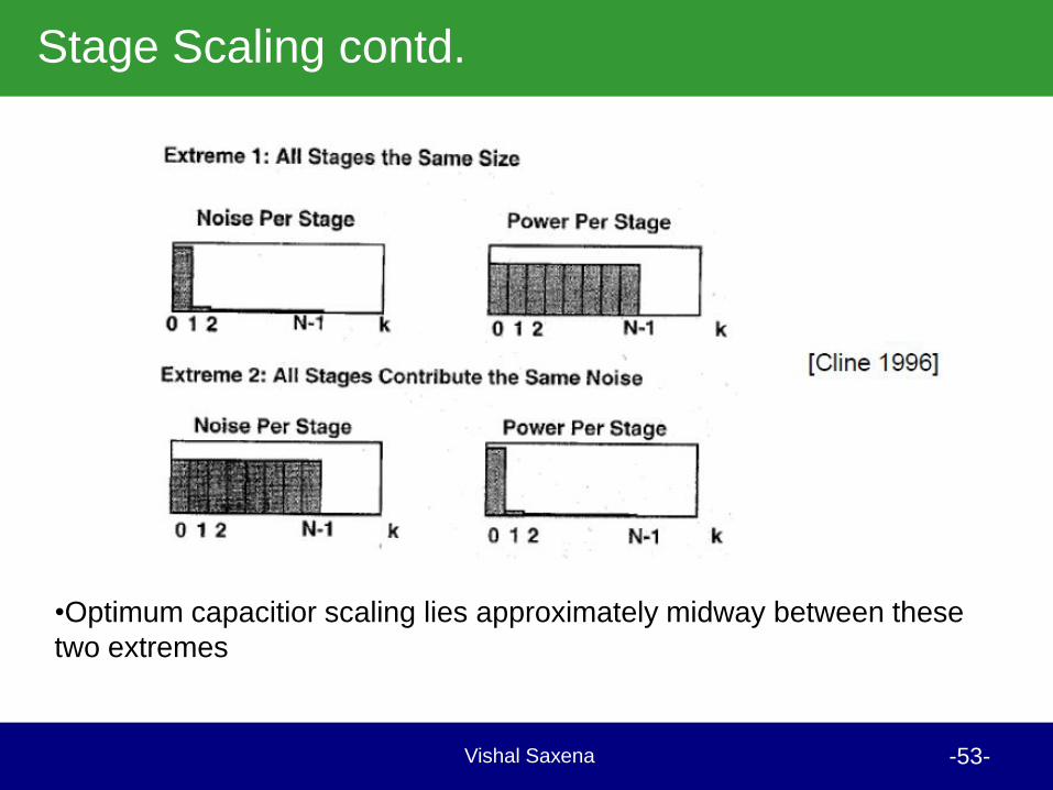
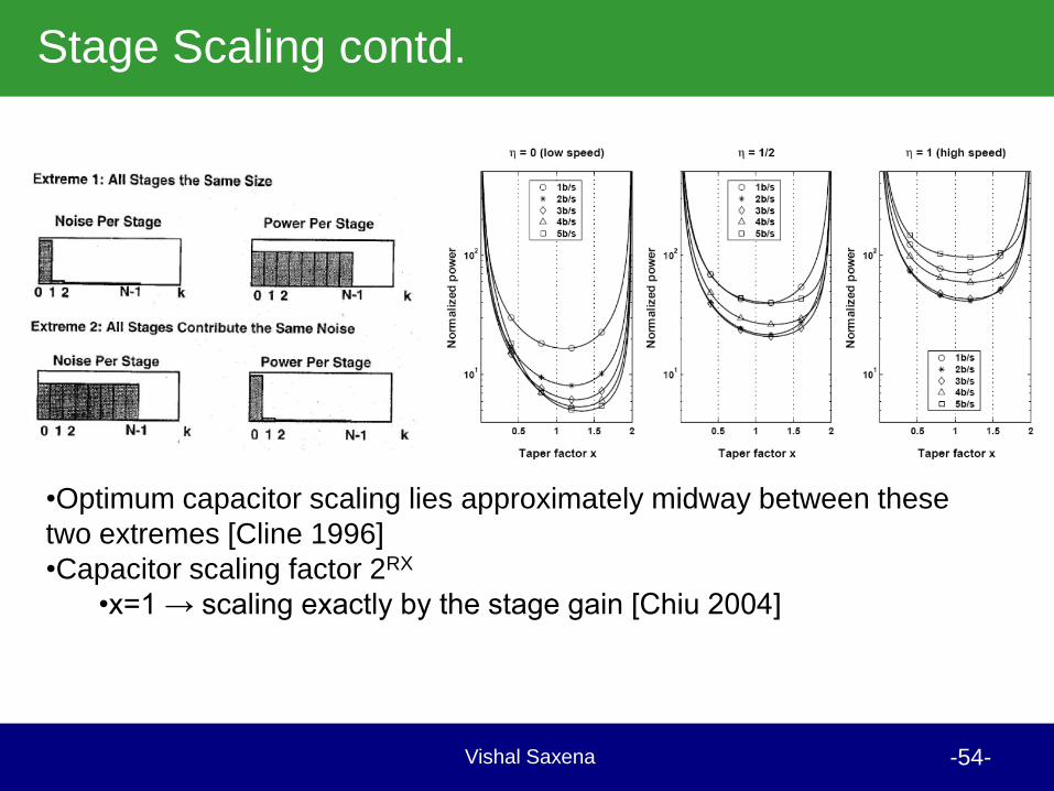
Stage Scaling contd.
•Optimum capacitior scaling lies approximately midway between these
two extremes
Vishal Saxena -54-
Stage Scaling contd.
•Optimum capacitor scaling lies approximately midway between these
two extremes [Cline 1996]
•Capacitor scaling factor 2RX
•x=1 → scaling exactly by the stage gain [Chiu 2004]
Vishal Saxena -55-
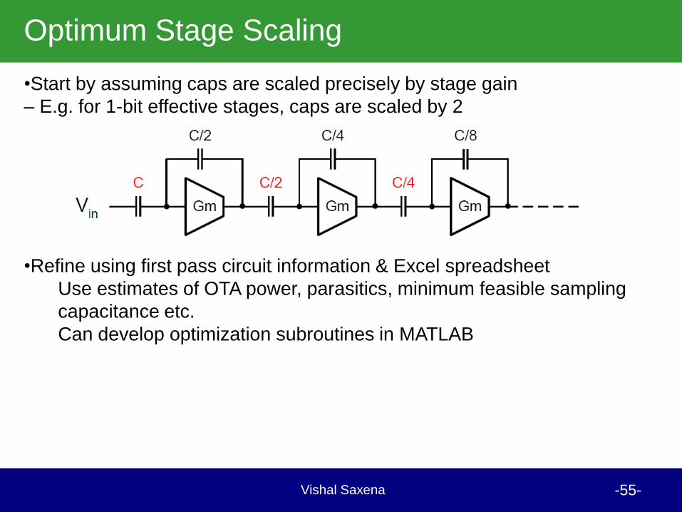
Optimum Stage Scaling
•Start by assuming caps are scaled precisely by stage gain
– E.g. for 1-bit effective stages, caps are scaled by 2
•Refine using first pass circuit information & Excel spreadsheet
Use estimates of OTA power, parasitics, minimum feasible sampling
capacitance etc.
Can develop optimization subroutines in MATLAB
Vishal Saxena -56-
How Many Bits per Stage?
Low per-stage resolution (e.g. 1-bit effective) – Need many stages
+ OTAs have small closed loop gain, large feedback factor
• High speed
High per-stage resolution (e.g. 3-bit effective) + Fewer stages
– OTAs can be power hungry, especially at high speed
– Significant loading from flash-ADC
Qualitative conclusion Use low per-stage resolution for very high speed designs
Try higher resolution stages when power efficiency is most important constraint
Vishal Saxena -57-
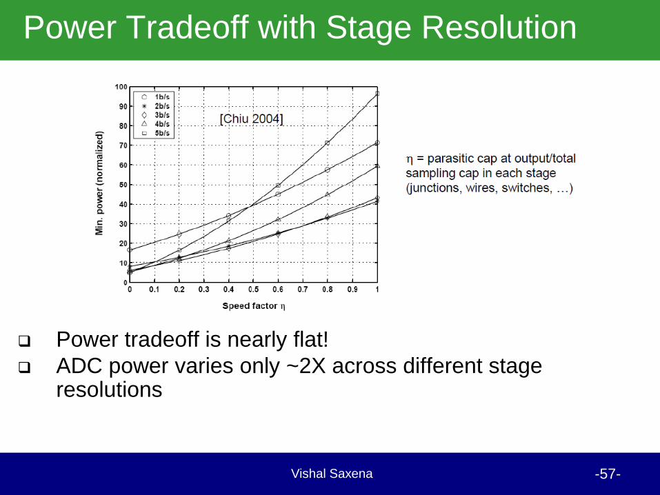
Power Tradeoff with Stage Resolution
Power tradeoff is nearly flat!
ADC power varies only ~2X across different stage resolutions
Vishal Saxena -58-
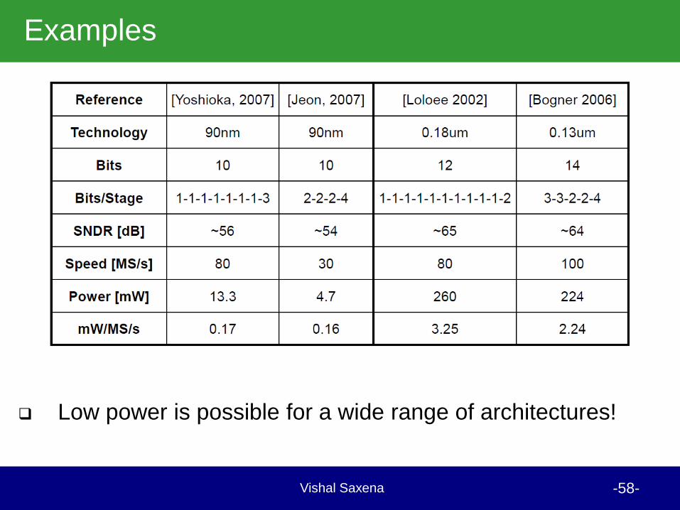
Examples
Low power is possible for a wide range of architectures!
Vishal Saxena -59-
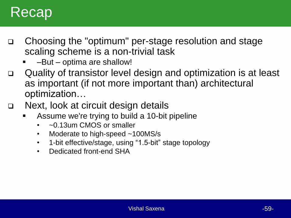
Recap
Choosing the "optimum" per-stage resolution and stage scaling scheme is a non-trivial task –But – optima are shallow!
Quality of transistor level design and optimization is at least as important (if not more important than) architectural optimization…
Next, look at circuit design details Assume we're trying to build a 10-bit pipeline
• ~0.13um CMOS or smaller
• Moderate to high-speed ~100MS/s
• 1-bit effective/stage, using “1.5-bit” stage topology
• Dedicated front-end SHA
Vishal Saxena -60-
References
1. Rudy van de Plassche, “CMOS Integrated Analog-to-Digital and Digital-to-Analog Converters,” 2nd Ed., Springer, 2005.
2. M. Gustavsson, J. Wikner, N. Tan, CMOS Data Converters for Communications, Kluwer Academic Publishers, 2000.
3. N. Krishnapura, Pipelined Analog to Digital Converters Slides, IIT Madras, 2009.
4. Y. Chiu, Data Converters Lecture Slides, UT Dallas 2012.
5. B. Boser, Analog-Digital Interface Circuits Lecture Slides, UC Berkeley 2011.
6. K. Nagaraj et al., “A 250-mW, 8-b, 52-Msamples/s parallel-pipelined A/D converter with reduced number of amplifiers”, IEEE Journal of Solid-State Circuits, pp. 312-320, vol. 32, no. 3, March 1997.
7. S. Kulhalli et al., “A 30mW 12b 21MSample/s pipelined CMOS ADC”, 2002 IEEE International Solid State Conference, pp. 18.4, vol. I, pp. 248-249,492, vol. II.
8. N. Sasidhar et al., “A Low Power Pipelined ADC Using Capacitor and Opamp Sharing Technique With a Scheme to Cancel the Effect of Signal Dependent Kickback”, IEEE Journal of Solid State Conference, pp. 2392-2401, vol. 44, no. 9, Sep 2009.
Vishal Saxena -61-
References
Implementation T. Cho, "Low-Power Low-Voltage Analog-to-Digital Conversion Techniques using Pipelined
Architecures, PhD Dissertation, UC Berkeley, 1995, http://kabuki.eecs.berkeley.edu/~tcho/Thesis1.pdf.
L. A. Singer at al., "A 14-bit 10-MHz calibration-free CMOS pipelined A/D converter," VLSI Circuit Symposium, pp. 94-95, Jun. 1996.
A. Abo, "Design for Reliability of Low-voltage, Switched-capacitor Circuits," PhD Dissertation, UC Berkeley, 1999, http://kabuki.eecs.berkeley.edu/~abo/abothesis.pdf.
D. Kelly et al., "A 3V 340mW 14b 75MSPS CMOS ADC with 85dB SFDR at Nyquist," ISSCC Dig. Techn. Papers, pp. 134-135, Feb. 2001.
A. Loloee, et. al, “A 12b 80-MSs Pipelined ADC Core with 190 mW Consumption from 3 V in 0.18-um, Digital CMOS”, Proc. ESSCIRC, pp. 467-469, 2002
B.-M. Min et al., "A 69-mW 10-bit 80-MSample/s Pipelined CMOS ADC," IEEE JSSC, pp. 2031-2039, Dec. 2003.
Y. Chiu, et al., "A 14-b 12-MS/s CMOS pipeline ADC with over 100-dB SFDR,” IEEE JSSC, pp. 2139-2151, Dec. 2004.
S. Limotyrakis et al., "A 150-MS/s 8-b 71-mW CMOS time-interleaved ADC," IEEE JSSC, pp. 1057-1067, May 2005.
T. N. Andersen et al., "A Cost-Efficient High-Speed 12-bit Pipeline ADC in 0.18-um Digital CMOS," IEEE JSSC, pp. 1506-1513, Jul 2005.
Vishal Saxena -62-
References
P. Bogner et al., "A 14b 100MS/s digitally self-calibrated pipelined ADC in 0.13um CMOS," ISSCC
Dig. Techn. Papers, pp. 832-833, Feb. 2006.
D. Kurose et al., "55-mW 200-MSPS 10-bit Pipeline ADCs for Wireless Receivers," IEEE JSSC, pp. 1589-1595, Jul. 2006.
S. Bardsley et al., "A 100-dB SFDR 80-MSPS 14-Bit 0.35um BiCMOS Pipeline ADC," IEEE JSSC, pp. 2144-2153, Sep. 2006.
A. M. A. Ali et al, "A 14-bit 125 MS/s IF/RF Sampling Pipelined ADC With 100 dB SFDR and 50 fs Jitter," IEEE JSSC, pp. 1846-1855, Aug. 2006.
S. K. Gupta, "A 1-GS/s 11-bit ADC With 55-dB SNDR, 250-mW Power Realized by a High Bandwidth Scalable Time-Interleaved Architecture," IEEE JSSC, 2650-2657, Dec. 2006.
M. Yoshioka et al., "A 0.8V 10b 80MS/s 6.5mW Pipelined ADC with Regulated Overdrive Voltage Biasing," ISSCC Dig. Techn. Papers, pp. 452-453, Feb. 2007.
Y.-D. Jeon et al., "A 4.7mW 0.32mm2 10b 30MS/s Pipelined ADC Without a Front-End S/H in 90nm CMOS," ISSCC Dig. Techn. Papers, pp. 456-457, Feb. 2007.
K.-H. Lee et al., "Calibration-free 14b 70MS/s 0.13um CMOS pipeline A/D converters based on highmatching 3D symmetric capacitors," Electronics Letters, pp. 35-36, Mar. 15, 2007.
K. Honda et al., "A Low-Power Low-Voltage 10-bit 100-MSample/s Pipeline A/D Converter Using Capacitance Coupling Techniques," IEEE JSSC, pp. 757-765, Apr. 2007.
Vishal Saxena -63-
References
Per-Stage Resolution and Stage Scaling D. W. Cline et al., "A power optimized 13-b 5 MSamples/s pipelined analog-to-digital converter in
1.2um CMOS," IEEE JSSC, Mar. 1996
Y. Chiu, "High-Performance Pipeline A/D Converter Design in Deep-Submicron CMOS," PhD Dissertation, UC Berkeley, 2004.
H. Ishii et al., "A 1.0 V 40mW 10b 100MS/s pipeline ADC in 90nm CMOS," Proc. CICC, pp. 395-398, Sep. 2005.
OTA Design, Noise B. E. Boser, "Analog Circuit Design with Submicron Transistors," Presentation at IEEE Santa Clara
Valley, May 19, 2005, http://www.ewh.ieee.org/r6/scv/ssc/May1905.htm
B. Murmann, EE315A Course Material, http://ccnet.stanford.edu/cgi-bin/handouts.cgi?cc=ee315a
R. Schreier et al., "Design-oriented estimation of thermal noise in switched-capacitor circuits," IEEE TCAS I, pp. 2358-2368, Nov. 2005.
Capacitor Matching Data C. H. Diaz et al., "CMOS technology for MS/RF SoC," IEEE Trans. Electron Devices, pp. 557-566,
Mar. 2003.
A. Verma et al., "Frequency-Based Measurement of Mismatches Between Small Capacitors," Proc. CICC, pp. 481-484, Sep. 2006.
Reference Generator T. L. Brooks et al., "A low-power differential CMOS bandgap reference," ISSCC Dig. Techn. Papers,
pp. 248-249, Feb. 1994.
Vishal Saxena -64-
References
Digitally-Assisted Pipelined B. Murmann et al., "A 12-bit 75-MS/s Pipelined ADC using Open-Loop Residue Amplification," IEEE
JSSC, pp. 2040-2050, Dec. 2003.
J. Fiorenza et al., "Comparator-Based Switched-Capacitor Circuits for Scaled CMOS Technologies, " IEEE JSSC, pp. 2658-2668, Dec. 2006.
E. Iroaga et al. "A 12b, 75MS/s Pipelined ADC Using Incomplete Settling," IEEE JSSC, pp. 748-756, Apr. 2007.
J. Hu, N. Dolev and B. Murmann, "A 9.4-bit, 50-MS/s, 1.44-mW Pipelined ADC using Dynamic Residue Amplification,“ VLSI Circuits Symposium, June 2008.