Embed Size (px)
Citation preview
Analog to Digital Converters for DC-DC converters with digital control
Maria João Perdigão Barradas Instituto Superior Técnico, TU Lisbon
Abstract – This work proposes an A/D converter that quantizes the difference between the output voltage of a DC-DC buck converter and the desired value on the output. Two A/D converters, each one based on a single comparator, were designed to integrate two different DC-DC converters, one of them with eight outputs, non-linear quantization intervals and working with 2 MHz, and the other one working with a 20 MHz frequency and with two outputs.
This solution leads to the design of A/D converts in 130 nm UMC® technology, which allow the digital control to sense transient variation in the output voltage of the DC-DC in less than 10% of a clock period.
Keywords - DC-DC Converters with digital control; A/D Converters; Comparators; Comparators with multiple output
I. INTRODUCTION
In the last years the industry of consumer’s electronics has experimented extraordinary advances in terms of number of functionalities that are available inside computers and cell phones, for example. These extraordinary advances require efficient power management solutions in order to supply lots of complex circuits without losing batteries’ life span. A solution to manage efficiently the power consumption in these devices is the use of DC-DC buck converters as the one depicted on Figure 1, that convert the voltage of the battery in a lower voltage, in order to supply the electronic components at their proper voltage level.
Figure 1. DC-DC buck converter.
Despite the high efficiency of the DC-DC buck converters, typically between 80 and 98%, their design is not simple. The complexity of their design is motivated by the need of keep the output voltage at a desired value with the minimum ripple possible. That claims for control circuits which are able to regulate the output voltage when a line or a load transient oc-curs. A line variation means changes in the battery, like its discharge. The load variations occur when the load conditions are changed.
The purpose of the control laws is to regulate of the output value by adjusting the time during the power switches sw1 and sw2 are on. According to equations (1) and (2) since the mean value of the inductor voltage is zero in steady-state, the output voltage is related to the input voltage by the percentage of the clock period when sw1 is on (duty-cycle, D). The purpose of
the control circuit is to adapt the duty-cycle to obtain the de-sired value at the output.
��(�) = �� − ��, 0 < � < ��−��,�� < � < � (1)
< �� >= 0 ⇔1�� � − ���� +1�� −�����
��
��
�= 0⇔ � = ���
(2)
In the last years the techniques used to control the output voltage of the DC-DC buck converter have been changing from the analog domain to the digital domain, since the digital domain allows the implementation of more accurate, fast, complex and flexible control laws [1].
Despite the advantages of this migration from the analog domain to the digital domain, the use of digital control laws involve the use of analog to digital (ADC) and digital to analog (DAC) converters, because the state values of the DC-DC are analog. The purpose of the ADC in these power conversion systems is the quantization between the voltage sensed at the DC-DC output and the desired value at the output.
II. ANALOG TO DIGITAL CONVERTERS FOR DC-DC
CONVERTERS WITH DIGITAL CONTROL
A. Introduction
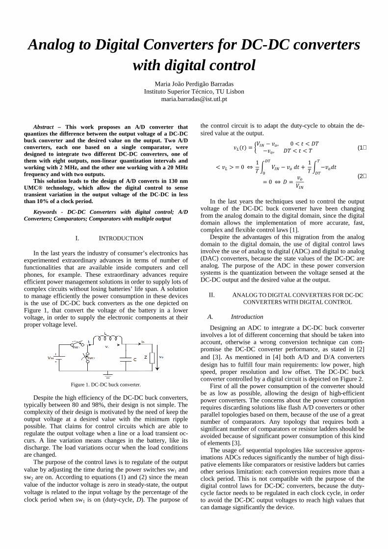
Designing an ADC to integrate a DC-DC buck converter involves a lot of different concerning that should be taken into account, otherwise a wrong conversion technique can com-promise the DC-DC converter performance, as stated in [2] and [3]. As mentioned in [4] both A/D and D/A converters design has to fulfill four main requirements: low power, high speed, proper resolution and low offset. The DC-DC buck converter controlled by a digital circuit is depicted on Figure 2.
First of all the power consumption of the converter should be as low as possible, allowing the design of high-efficient power converters. The concerns about the power consumption requires discarding solutions like flash A/D converters or other parallel topologies based on them, because of the use of a great number of comparators. Any topology that requires both a significant number of comparators or resistor ladders should be avoided because of significant power consumption of this kind of elements [3].
The usage of sequential topologies like successive approx-imations ADCs reduces significantly the number of high dissi-pative elements like comparators or resistive ladders but carries other serious limitation: each conversion requires more than a clock period. This is not compatible with the purpose of the digital control laws for DC-DC converters, because the duty-cycle factor needs to be regulated in each clock cycle, in order to avoid the DC-DC output voltages to reach high values that can damage significantly the device.
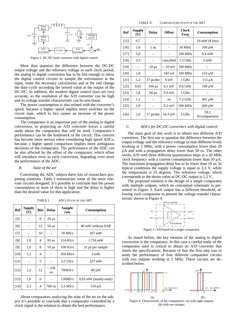
Figure 2. DC-DC buck converter with digital control.
More than quantize the difference between the DC-DC output voltage and the reference voltage in each clock period, the analog to digital conversion has to be fast enough to allow the digital control circuits to sample the information at the input, make the necessary calculations and at the end change the duty-cycle according the sensed value at the output of the DC-DC. In addition, the modern digital control laws are very accurate, so the resolution of the A/D converter can be high and its voltage transfer characteristic can be non-linear.
The power consumption is also related with the converter’s speed, because a higher speed implies more switches on the circuit state, which in fact causes an increase of the power consumption.
The comparator is an important part of the analog to digital conversion, so projecting an A/D converter forces a careful study about the comparator that will be used. Comparator’s performance can be the bottleneck of the circuit. This concern has become more serious when considering high speed ADCs, because a higher speed comparison implies more ambiguous decisions of the comparator. The performance of the ADC can be also affected by the offset of the comparator, which offset will introduce error in each conversion, degrading even more the performance of the ADC.
B. State of the art
Concerning the ADC subject there lots of researchers pro-posing solutions. Table I summarizes some of the most rele-vant circuits designed. It’s possible to conclude that the power consumption in most of them is high and the delay is higher than the desired value for this application.
TABLE I. ADCS STATE OF THE ART
Ref Supply [V] Bits Delay Sample
rate Consumption
[5] - 8 20 µs - -
[6] - 12 50 µs - 40 mW without SAR
[7] - 10 - 70 MS/s 267 mW
[8] 1,8 4 93 ns 114 KS/s 1,716 mW
[9] 1,0 8 10 µs 100 KS/s 31 pJ per sample
[10] 1,5 4 - 104 MS/s 3 mW
[11] - 5 - 3.5 GS/s 227 mW
[12] 1,2 12 ~ 230
ns 700KS/s 40 µW
[13] 1,0 6 - 130MS/s 0,63 mW (steady-state)
[14] 2,3 4 700 ns 5.5 MS/s 119 µA
About comparators analyzing the state of the art on the sub-ject it’s possible to conclude that a comparator controlled by a clock signal is the solution to obtain the best performance.
TABLE II. COMPARATORS STATE OF THE ART
Ref Supply [V] Delay Offset Clock
Freq Consumption
[15] 0,7 - - - 19 mW (8 bits)
[16] 1,0 1 ns - 50 MHz 100 µW
[17] 5,0 - - 100 MHz 0.4 mW
[18] 3,3 - cancelled 1.3 GHz 2 mW
[19] - 10 ps < 10 mV 100 MHz -
[20] 1,8 - 182 nA 100 MHz 153 µW
[21] 1,2 37 ps/dec 8 mV 1 GHz 113 µA
[22] 0,65 104 ps 6.1 mV 0.6 GHz 108 µW
[23] 1,8 60 ps 0.9 mV 1 GHz -
[24] 1,2 - ne 7.2 GHz 461 µW
[25] 1,8 - 0.2 mV 500 MHz 600 µW
[26] 1,0 17 ps/dec 16.3 mV 3 GHz 59.2
fJ/comparision
C. ADCs for DC-DC converters with digital control
The main goal of this work is to obtain two different A/D converters. The first one to quantize the difference between the output voltage and the reference voltage in nine different levels working at 2 MHz, with a power consumption lower than 20 µA and with a propagation delay lower than 50 ns. The other works A/D with three different quantization steps at a 20 MHz clock frequency with a current consumption lower than 50 µA. The maximum propagation delay has to be lower than 10 ns. In typical conditions the supply voltage is equal to 3,3 V, while the temperature is 25 degrees. The reference voltage, which corresponds to the desire value at DC-DC output is 1,2 V.
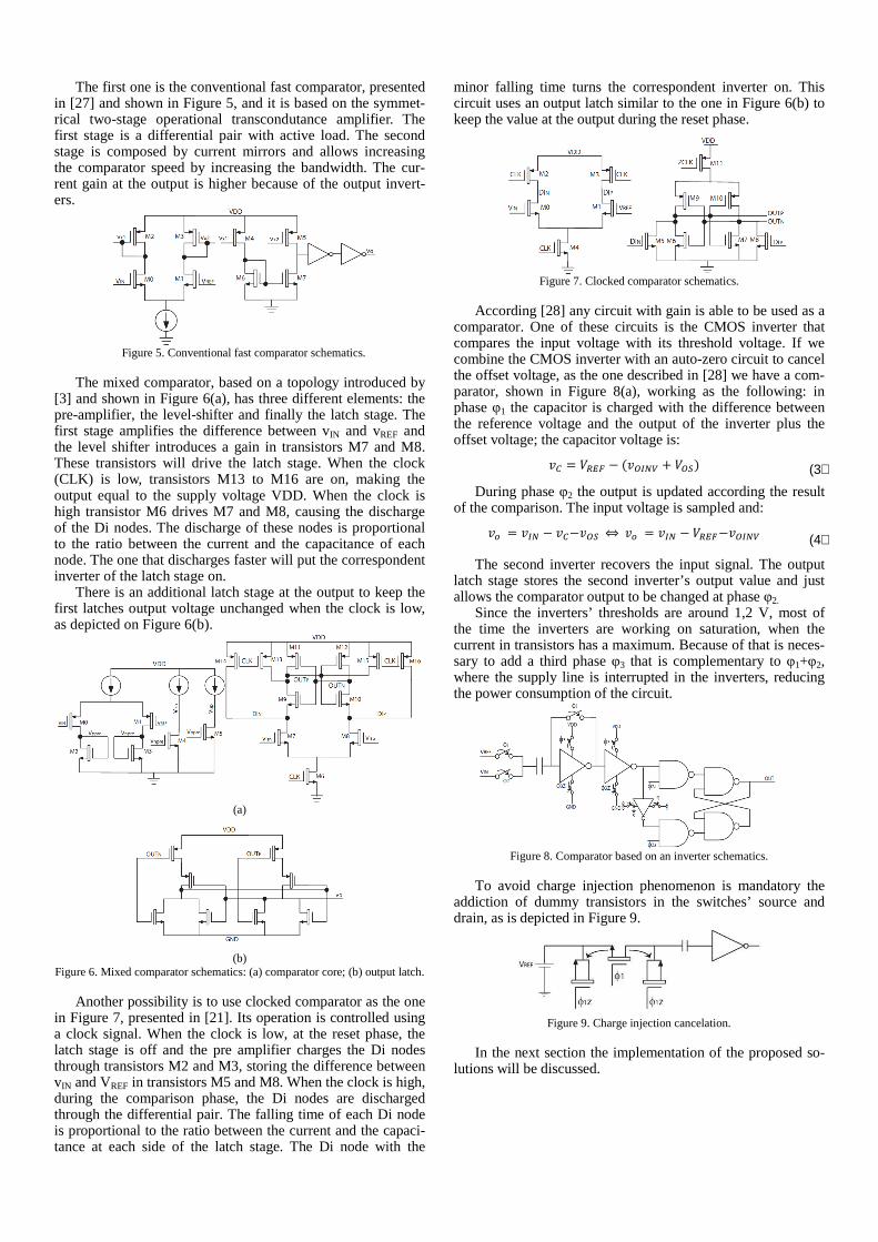
The proposed solution is the design of a single comparator with multiple outputs, which its conceptual schematic is pre-sented in Figure 3. Each output has a different threshold, al-lowing each comparator to present the voltage transfer charac-teristic shown in Figure 4.
Figure 3. A/D based on a single comparator.
As stated before, the key element of the analog to digital conversion is the comparator. In this case a careful study of the comparator used is critical to obtain an A/D converter that meets the specifications. Because of that the first step was to study the performance of four different comparator circuits with two outputs working at 2 MHz. These circuits are de-scribed below.
(a) (b)
Figure 4. Characteristic of the comparators: (a) with eight outputs; (b) with two outupts.
The first one is the conventional fast comparator, presented in [27] and shown in Figure 5, and it is based on the symmet-rical two-stage operational transcondutance amplifier. The first stage is a differential pair with active load. The second stage is composed by current mirrors and allows increasing the comparator speed by increasing the bandwidth. The cur-rent gain at the output is higher because of the output invert-ers.
Figure 5. Conventional fast comparator schematics.
The mixed comparator, based on a topology introduced by [3] and shown in Figure 6(a), has three different elements: the pre-amplifier, the level-shifter and finally the latch stage. The first stage amplifies the difference between vIN and vREF and the level shifter introduces a gain in transistors M7 and M8. These transistors will drive the latch stage. When the clock (CLK) is low, transistors M13 to M16 are on, making the output equal to the supply voltage VDD. When the clock is high transistor M6 drives M7 and M8, causing the discharge of the Di nodes. The discharge of these nodes is proportional to the ratio between the current and the capacitance of each node. The one that discharges faster will put the correspondent inverter of the latch stage on.
There is an additional latch stage at the output to keep the first latches output voltage unchanged when the clock is low, as depicted on Figure 6(b).
(a)
(b)
Figure 6. Mixed comparator schematics: (a) comparator core; (b) output latch.
Another possibility is to use clocked comparator as the one in Figure 7, presented in [21]. Its operation is controlled using a clock signal. When the clock is low, at the reset phase, the latch stage is off and the pre amplifier charges the Di nodes through transistors M2 and M3, storing the difference between vIN and VREF in transistors M5 and M8. When the clock is high, during the comparison phase, the Di nodes are discharged through the differential pair. The falling time of each Di node is proportional to the ratio between the current and the capaci-tance at each side of the latch stage. The Di node with the
minor falling time turns the correspondent inverter on. This circuit uses an output latch similar to the one in Figure 6(b) to keep the value at the output during the reset phase.
Figure 7. Clocked comparator schematics.
According [28] any circuit with gain is able to be used as a comparator. One of these circuits is the CMOS inverter that compares the input voltage with its threshold voltage. If we combine the CMOS inverter with an auto-zero circuit to cancel the offset voltage, as the one described in [28] we have a com-parator, shown in Figure 8(a), working as the following: in phase φ1 the capacitor is charged with the difference between the reference voltage and the output of the inverter plus the offset voltage; the capacitor voltage is:
�� = ���� − (� ! + � ") (3)
During phase φ2 the output is updated according the result of the comparison. The input voltage is sampled and:
�� = � − ��−� " ⇔�� = � − ����−� ! (4)
The second inverter recovers the input signal. The output latch stage stores the second inverter’s output value and just allows the comparator output to be changed at phase φ2.
Since the inverters’ thresholds are around 1,2 V, most of the time the inverters are working on saturation, when the current in transistors has a maximum. Because of that is neces-sary to add a third phase φ3 that is complementary to φ1+φ2, where the supply line is interrupted in the inverters, reducing the power consumption of the circuit.
Figure 8. Comparator based on an inverter schematics.
To avoid charge injection phenomenon is mandatory the addiction of dummy transistors in the switches’ source and drain, as is depicted in Figure 9.
Figure 9. Charge injection cancelation.
In the next section the implementation of the proposed so-lutions will be discussed.
III. IMPLEMENTATION
A. Preliminary study
In order to choose the best comparator for the application, four comparators with two outputs and thresholds for ± 5 mV at 2 MHz will be designed, each one based on one of the topol-ogies presented in Section II.
For the conventional fast comparator the solution was to duplicate the output stage to have two different outputs, as shown in Figure 10(a). The two different thresholds are created increasing the channel width W of: transistor M6, to reinforce the pull-down and move the characteristic to +5mV; transistor M8, in order to move the characteristic to -5mV by reinforcing the pull-up. The circuit behavior is illustrated in Figure 10(b) by illustrating the current in the current mirrors.
(a)
(b) Figure 10. Conventional fast comparator with two ouptups: (a) schematics; (b)
behaviour.
The solution found to add two outputs to the mixed com-parator and to the clocked compactor was to duplicate the latch stages, each one with the proper threshold, to ensure a signifi-cant power saving comparing with the solution of duplicating the pre-amplifier or other analog stage that has static power dissipation.
Figure 11. Mixed comparator with two output.
(a) (b)
(c) (d)
(e) (f) Figure 12. Mixed comparator behaviour: .(a) input signals; (b) output voltage;
(c) (d) voltage at Di nodes; (e) (f) back-to-back inverter output.
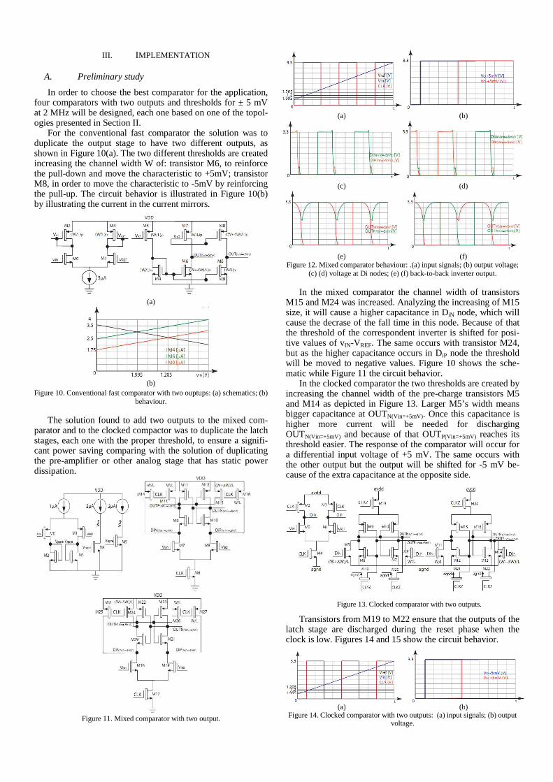
In the mixed comparator the channel width of transistors M15 and M24 was increased. Analyzing the increasing of M15 size, it will cause a higher capacitance in DiN node, which will cause the decrase of the fall time in this node. Because of that the threshold of the correspondent inverter is shifted for posi-tive values of vIN-VREF. The same occurs with transistor M24, but as the higher capacitance occurs in DiP node the threshold will be moved to negative values. Figure 10 shows the sche-matic while Figure 11 the circuit behavior.
In the clocked comparator the two thresholds are created by increasing the channel width of the pre-charge transistors M5 and M14 as depicted in Figure 13. Larger M5’s width means bigger capacitance at OUTN(Vin=+5mV). Once this capacitance is higher more current will be needed for discharging OUTN(Vin=+5mV) and because of that OUTP(Vin=+5mV) reaches its threshold easier. The response of the comparator will occur for a differential input voltage of +5 mV. The same occurs with the other output but the output will be shifted for -5 mV be-cause of the extra capacitance at the opposite side.
Figure 13. Clocked comparator with two outputs.
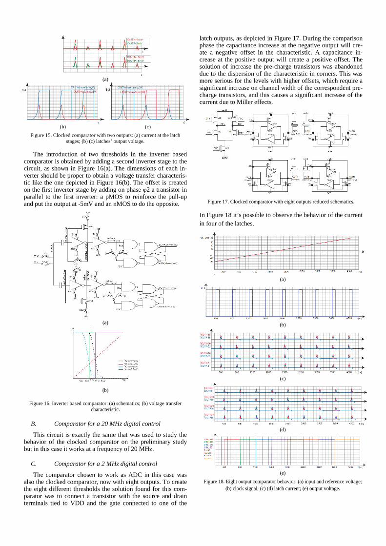
Transistors from M19 to M22 ensure that the outputs of the latch stage are discharged during the reset phase when the clock is low. Figures 14 and 15 show the circuit behavior.
(a) (b) Figure 14. Clocked comparator with two outputs: (a) input signals; (b) output
voltage.
(a)
(b) (c)
Figure 15. Clocked comparator with two outputs: (a) current at the latch stages; (b) (c) latches’ output voltage.
The introduction of two thresholds in the inverter based comparator is obtained by adding a second inverter stage to the circuit, as shown in Figure 16(a). The dimensions of each in-verter should be proper to obtain a voltage transfer characteris-tic like the one depicted in Figure 16(b). The offset is created on the first inverter stage by adding on phase φ2 a transistor in parallel to the first inverter: a pMOS to reinforce the pull-up and put the output at -5mV and an nMOS to do the opposite.
(a)
(b)
Figure 16. Inverter based comparator: (a) schematics; (b) voltage transfer characteristic.
B. Comparator for a 20 MHz digital control
This circuit is exactly the same that was used to study the behavior of the clocked comparator on the preliminary study but in this case it works at a frequency of 20 MHz.
C. Comparator for a 2 MHz digital control
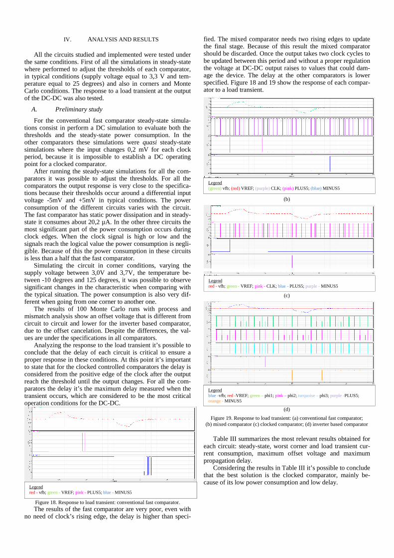
The comparator chosen to work as ADC in this case was also the clocked comparator, now with eight outputs. To create the eight different thresholds the solution found for this com-parator was to connect a transistor with the source and drain terminals tied to VDD and the gate connected to one of the
latch outputs, as depicted in Figure 17. During the comparison phase the capacitance increase at the negative output will cre-ate a negative offset in the characteristic. A capacitance in-crease at the positive output will create a positive offset. The solution of increase the pre-charge transistors was abandoned due to the dispersion of the characteristic in corners. This was more serious for the levels with higher offsets, which require a significant increase on channel width of the correspondent pre-charge transistors, and this causes a significant increase of the current due to Miller effects.
Figure 17. Clocked comparator with eight outputs reduced schematics.
In Figure 18 it’s possible to observe the behavior of the current in four of the latches.
(a)
(b)
(c)
(d)
(e)
Figure 18. Eight output comparator behavior: (a) input and reference voltage; (b) clock signal; (c) (d) latch current; (e) output voltage.
IV. ANALYSIS AND RESULTS
All the circuits studied and implemented were tested under the same conditions. First of all the simulations in steady-state where performed to adjust the thresholds of each comparator, in typical conditions (supply voltage equal to 3,3 V and tem-perature equal to 25 degrees) and also in corners and Monte Carlo conditions. The response to a load transient at the output of the DC-DC was also tested.
A. Preliminary study
For the conventional fast comparator steady-state simula-tions consist in perform a DC simulation to evaluate both the thresholds and the steady-state power consumption. In the other comparators these simulations were quasi steady-state simulations where the input changes 0,2 mV for each clock period, because it is impossible to establish a DC operating point for a clocked comparator.
After running the steady-state simulations for all the com-parators it was possible to adjust the thresholds. For all the comparators the output response is very close to the specifica-tions because their thresholds occur around a differential input voltage -5mV and +5mV in typical conditions. The power consumption of the different circuits varies with the circuit. The fast comparator has static power dissipation and in steady-state it consumes about 20,2 µA. In the other three circuits the most significant part of the power consumption occurs during clock edges. When the clock signal is high or low and the signals reach the logical value the power consumption is negli-gible. Because of this the power consumption in these circuits is less than a half that the fast comparator.
Simulating the circuit in corner conditions, varying the supply voltage between 3,0V and 3,7V, the temperature be-tween -10 degrees and 125 degrees, it was possible to observe significant changes in the characteristic when comparing with the typical situation. The power consumption is also very dif-ferent when going from one corner to another one.
The results of 100 Monte Carlo runs with process and mismatch analysis show an offset voltage that is different from circuit to circuit and lower for the inverter based comparator, due to the offset cancelation. Despite the differences, the val-ues are under the specifications in all comparators.
Analyzing the response to the load transient it’s possible to conclude that the delay of each circuit is critical to ensure a proper response in these conditions. At this point it’s important to state that for the clocked controlled comparators the delay is considered from the positive edge of the clock after the output reach the threshold until the output changes. For all the com-parators the delay it’s the maximum delay measured when the transient occurs, which are considered to be the most critical operation conditions for the DC-DC.
Figure 18. Response to load transient: conventional fast comparator. The results of the fast comparator are very poor, even with
no need of clock’s rising edge, the delay is higher than speci-
fied. The mixed comparator needs two rising edges to update the final stage. Because of this result the mixed comparator should be discarded. Once the output takes two clock cycles to be updated between this period and without a proper regulation the voltage at DC-DC output raises to values that could dam-age the device. The delay at the other comparators is lower specified. Figure 18 and 19 show the response of each compar-ator to a load transient.
(b)
(c)
(d)
Figure 19. Response to load transient: (a) conventional fast comparator; (b) mixed comparator (c) clocked comparator; (d) inverter based comparator
Table III summarizes the most relevant results obtained for each circuit: steady-state, worst corner and load transient cur-rent consumption, maximum offset voltage and maximum propagation delay.
Considering the results in Table III it’s possible to conclude that the best solution is the clocked comparator, mainly be-cause of its low power consumption and low delay.
Legend red - vfb; green - VREF; pink - PLUS5; blue - MINUS5
Legend (green) vfb; (red) VREF; (purple) CLK; (pink) PLUS5; (blue) MINUS5
Legend red - vfb; green - VREF; pink - CLK; blue - PLUS5; purple - MINUS5
Legend blue -vfb; red -VREF; green – phi1; pink – phi2; turquoise – phi3; purple -PLUS5; orange - MINUS5
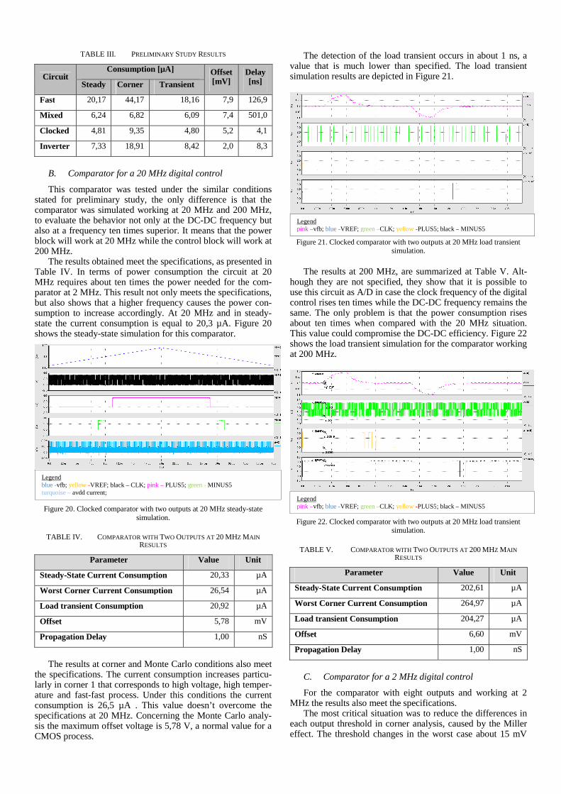
TABLE III. PRELIMINARY STUDY RESULTS
Circuit Consumption [µA] Offset
[mV] Delay [ns] Steady Corner Transient
Fast 20,17 44,17 18,16 7,9 126,9
Mixed 6,24 6,82 6,09 7,4 501,0
Clocked 4,81 9,35 4,80 5,2 4,1
Inverter 7,33 18,91 8,42 2,0 8,3
B. Comparator for a 20 MHz digital control
This comparator was tested under the similar conditions stated for preliminary study, the only difference is that the comparator was simulated working at 20 MHz and 200 MHz, to evaluate the behavior not only at the DC-DC frequency but also at a frequency ten times superior. It means that the power block will work at 20 MHz while the control block will work at 200 MHz.
The results obtained meet the specifications, as presented in Table IV. In terms of power consumption the circuit at 20 MHz requires about ten times the power needed for the com-parator at 2 MHz. This result not only meets the specifications, but also shows that a higher frequency causes the power con-sumption to increase accordingly. At 20 MHz and in steady-state the current consumption is equal to 20,3 µA. Figure 20 shows the steady-state simulation for this comparator.
Figure 20. Clocked comparator with two outputs at 20 MHz steady-state simulation.
TABLE IV. COMPARATOR WITH TWO OUTPUTS AT 20 MHZ MAIN RESULTS
Parameter Value Unit
Steady-State Current Consumption 20,33 µA
Worst Corner Current Consumption 26,54 µA
Load transient Consumption 20,92 µA
Offset 5,78 mV
Propagation Delay 1,00 nS
The results at corner and Monte Carlo conditions also meet the specifications. The current consumption increases particu-larly in corner 1 that corresponds to high voltage, high temper-ature and fast-fast process. Under this conditions the current consumption is 26,5 µA . This value doesn’t overcome the specifications at 20 MHz. Concerning the Monte Carlo analy-sis the maximum offset voltage is 5,78 V, a normal value for a CMOS process.
The detection of the load transient occurs in about 1 ns, a value that is much lower than specified. The load transient simulation results are depicted in Figure 21.
Figure 21. Clocked comparator with two outputs at 20 MHz load transient simulation.
The results at 200 MHz, are summarized at Table V. Alt-hough they are not specified, they show that it is possible to use this circuit as A/D in case the clock frequency of the digital control rises ten times while the DC-DC frequency remains the same. The only problem is that the power consumption rises about ten times when compared with the 20 MHz situation. This value could compromise the DC-DC efficiency. Figure 22 shows the load transient simulation for the comparator working at 200 MHz.
Figure 22. Clocked comparator with two outputs at 20 MHz load transient simulation.
TABLE V. COMPARATOR WITH TWO OUTPUTS AT 200 MHZ MAIN RESULTS
Parameter Value Unit
Steady-State Current Consumption 202,61 µA
Worst Corner Current Consumption 264,97 µA
Load transient Consumption 204,27 µA
Offset 6,60 mV
Propagation Delay 1,00 nS
C. Comparator for a 2 MHz digital control
For the comparator with eight outputs and working at 2 MHz the results also meet the specifications.
The most critical situation was to reduce the differences in each output threshold in corner analysis, caused by the Miller effect. The threshold changes in the worst case about 15 mV
Legend blue -vfb; yellow -VREF; black – CLK; pink – PLUS5; green - MINUS5 turquoise – avdd current;
Legend pink –vfb; blue -VREF; green –CLK; yellow -PLUS5; black – MINUS5
Legend pink –vfb; blue -VREF; green –CLK; yellow -PLUS5; black – MINUS5
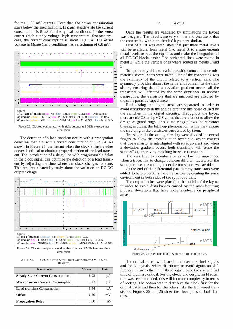
for the ± 35 mV outputs. Even that, the power consumption stays below the specifications. In quasi steady-state the current consumption is 8 µA for the typical conditions. In the worst corner (high supply voltage, high temperature, fast-fast pro-cess) the current consumption is about 11,1 µA. The offset voltage in Monte Carlo conditions has a maximum of 6,8 mV.
Figure 23. Clocked comparator with eight outputs at 2 MHz steady-state simulation.
The detection of a load transient occurs with a propagation delay less than 2 ns with a current consumption of 8,94 µA. As shown in Figure 23, the instant when the clock’s rinsing edge occurs is critical to obtain a proper detection of the load transi-ent. The introduction of a delay line with programmable delay in the clock signal can optimize the detection of a load transi-ent by adjusting the time where the clock changes its state. This requires a carefully study about the variation on DC-DC output voltage.
Figure 24. Clocked comparator with eight outputs at 2 MHz load transient
simulation.
TABLE VI. COMPARATOR WITH EIGHT OUTPUTS AT 2 MHZ MAIN RESULTS
Parameter Value Unit
Steady-State Current Consumption 8,03 µA
Worst Corner Current Consumption 11,13 µA
Load transient Consumption 8.94 µA
Offset 6,80 mV
Propagation Delay 1,60 nS
V. LAYOUT
Once the results are validated by simulations the layout was designed. The circuits are very similar and because of that the concerning with both circuits’ layout are similar.
First of all it was established that just three metal levels will be available, from metal 1 to metal 3, to ensure enough metal levels to rout the top lines and make the integration of all DC-DC blocks easier. The horizontal lines were routed in metal 2, while the vertical ones where routed in metals 1 and 3.
To optimize yield and avoid parasitic connections or mis-matches several cares were taken. One of the concerning was the symmetry of the circuit related to a vertical axis. The symmetry provides almost the same environment to the tran-sistors, ensuring that if a deviation gradient occurs all the transistors will affected by the same deviation. In another perspective, the transistors that are mirrored are affected by the same parasitic capacitance.
Both analog and digital areas are separated in order to avoid disturbances in the analog circuitry like noise caused by the switches in the digital circuitry. Throughout the layout there are nMOS and pMOS zones that are distinct to allow the design of guard rings. This guard rings allows the substract biasing avoiding the latch-up phenomenon, while they ensure the shielding of the transistors surrounded by them.
Transistors in the analog circuitry were divided in several fingers to allow the interdigitation technique, which ensures that one transistor is interdigited with its equivalent and when a deviation gradient occurs both transistors will sense the same effect, improving matching between transistors.
The vias have two contacts to make low the impedance when a traces has to change between different layers. For the same purposes the routing under the transistors was avoided.
At the end of the differential pair dummy transistors were added, to help protecting these transistors by creating the same environment in both sides of the symmetry axis.
The output latches were placed in the middle of the layout in order to avoid disturbances caused by the manufacturing process, deviations that have more incidence on peripheral areas.
Figure 25. Clocked comparator with two outputs floor plan.
The critical traces, which are in this case the clock signals and the Di signals, where distributed to avoid significant dif-ferences in traces that carry these signal, once the rise and fall time of them are critical. For the clock, and despite an H struc-ture was recommended, this will increase complexity in terms of rooting. The option was to distribute the clock first for the critical paths and then for the others, like the latch-reset tran-sistors. Figures 25 and 26 show the floor plans of both lay-outs.
Legend 1st, 2nd and 5th graphics pink –vfb; blue -VREF; green –CLK; pink – avdd current 3rd graphic yellow – PLUS35; pink –PLUS20; black – PLUS10; turquoise – PLUS5 4th graphic yellow – MINUS5; green –MINUS10; pink – ;MINUS20; blue – MINUS35
Legend 1st and 2nd graphics turquoise –vfb; yellow –VREF; green –CLK 3rd graphic pink – PLUS35; blue – PLUS20; green – PLUS10; black – PLUS5 4th graphic pink – MINUS5; blue –MINUS10; yellow – ;MINUS20; black – MINUS35
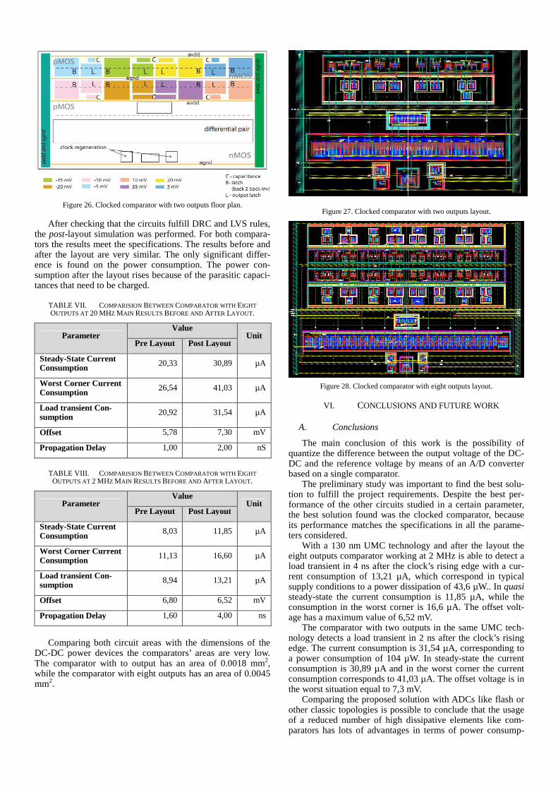
Figure 26. Clocked comparator with two outputs floor plan.
After checking that the circuits fulfill DRC and LVS rules, the post-layout simulation was performed. For both compara-tors the results meet the specifications. The results before and after the layout are very similar. The only significant differ-ence is found on the power consumption. The power con-sumption after the layout rises because of the parasitic capaci-tances that need to be charged.
TABLE VII. COMPARISION BETWEEN COMPARATOR WITH EIGHT OUTPUTS AT 20 MHZ MAIN RESULTS BEFORE AND AFTER LAYOUT.
Parameter Value
Unit Pre Layout Post Layout
Steady-State Current Consumption 20,33 30,89 µA
Worst Corner Current Consumption 26,54 41,03 µA
Load transient Con-sumption 20,92 31,54 µA
Offset 5,78 7,30 mV
Propagation Delay 1,00 2,00 nS
TABLE VIII. COMPARISION BETWEEN COMPARATOR WITH EIGHT OUTPUTS AT 2 MHZ MAIN RESULTS BEFORE AND AFTER LAYOUT.
Parameter Value
Unit Pre Layout Post Layout
Steady-State Current Consumption 8,03 11,85 µA
Worst Corner Current Consumption 11,13 16,60 µA
Load transient Con-sumption 8,94 13,21 µA
Offset 6,80 6,52 mV
Propagation Delay 1,60 4,00 ns
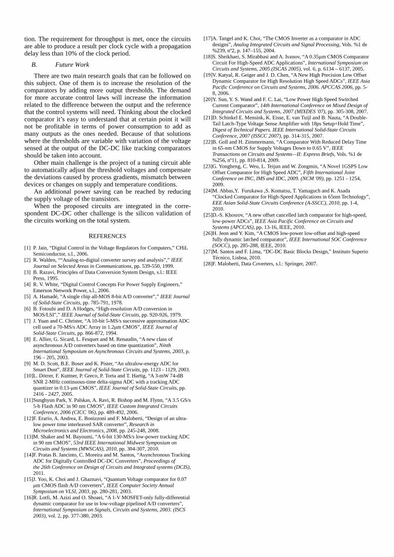
Comparing both circuit areas with the dimensions of the DC-DC power devices the comparators’ areas are very low. The comparator with to output has an area of 0.0018 mm2, while the comparator with eight outputs has an area of 0.0045 mm2.
Figure 27. Clocked comparator with two outputs layout.
Figure 28. Clocked comparator with eight outputs layout.
VI. CONCLUSIONS AND FUTURE WORK
A. Conclusions
The main conclusion of this work is the possibility of quantize the difference between the output voltage of the DC-DC and the reference voltage by means of an A/D converter based on a single comparator.
The preliminary study was important to find the best solu-tion to fulfill the project requirements. Despite the best per-formance of the other circuits studied in a certain parameter, the best solution found was the clocked comparator, because its performance matches the specifications in all the parame-ters considered.
With a 130 nm UMC technology and after the layout the eight outputs comparator working at 2 MHz is able to detect a load transient in 4 ns after the clock’s rising edge with a cur-rent consumption of 13,21 µA, which correspond in typical supply conditions to a power dissipation of 43,6 µW.. In quasi steady-state the current consumption is 11,85 µA, while the consumption in the worst corner is 16,6 µA. The offset volt-age has a maximum value of 6,52 mV.
The comparator with two outputs in the same UMC tech-nology detects a load transient in 2 ns after the clock’s rising edge. The current consumption is 31,54 µA, corresponding to a power consumption of 104 µW. In steady-state the current consumption is 30,89 µA and in the worst corner the current consumption corresponds to 41,03 µA. The offset voltage is in the worst situation equal to 7,3 mV.
Comparing the proposed solution with ADCs like flash or other classic topologies is possible to conclude that the usage of a reduced number of high dissipative elements like com-parators has lots of advantages in terms of power consump-
tion. The requirement for throughput is met, once the circuits are able to produce a result per clock cycle with a propagation delay less than 10% of the clock period.
B. Future Work
There are two main research goals that can be followed on this subject. One of them is to increase the resolution of the comparators by adding more output thresholds. The demand for more accurate control laws will increase the information related to the difference between the output and the reference that the control systems will need. Thinking about the clocked comparator it’s easy to understand that at certain point it will not be profitable in terms of power consumption to add as many outputs as the ones needed. Because of that solutions where the thresholds are variable with variation of the voltage sensed at the output of the DC-DC like tracking comparators should be taken into account.
Other main challenge is the project of a tuning circuit able to automatically adjust the threshold voltages and compensate the deviations caused by process gradients, mismatch between devices or changes on supply and temperature conditions.
An additional power saving can be reached by reducing the supply voltage of the transistors.
When the proposed circuits are integrated in the corre-spondent DC-DC other challenge is the silicon validation of the circuits working on the total system.
REFERENCES [1] P. Jain, “Digital Control in the Voltage Regulators for Computers,” CHiL
Semiconductor, s.l., 2006. [2] R. Walden, ““Analog-to-digital converter survey and analysis”,” IEEE
Journal on Selected Areas in Communications, pp. 539-550, 1999. [3] B. Razavi, Principles of Data Conversion System Design, s.l.: IEEE
Press, 1995. [4] R. V. White, “Digital Control Concepts For Power Supply Engineers,”
Emerson Network Power, s.l., 2006. [5] A. Hamadé, “A single chip all-MOS 8-bit A/D converter”,” IEEE Journal
of Solid-State Circuits, pp. 785-791, 1978. [6] B. Fotouhi and D. A Hodges, “High-resolution A/D conversion in
MOS/LSI”,” IEEE Journal of Solid-State Circuits, pp. 920-926, 1979. [7] J. Yuan and C. Christer, “A 10-bit 5-MS/s successive approximation ADC
cell used a 70-MS/s ADC Array in 1.2µm CMOS”, IEEE Journal of Solid-State Circuits, pp. 866-872, 1994.
[8] E. Allier, G. Sicard, L. Fesquet and M. Renaudin, “A new class of asynchronous A/D converters based on time quantization”, Ninth International Symposium on Asynchronous Circuits and Systems, 2003, p. 196 – 205, 2003.
[9] M. D. Scott, B.E. Boser and K. Pister, “An ultralow-energy ADC for Smart Dust”, IEEE Journal of Solid-State Circuits, pp. 1123 - 1129, 2003.
[10] L. Dörrer, F. Kuttner, P. Greco, P. Torta and T. Hartig, “A 3-mW 74-dB SNR 2-MHz continuous-time delta-sigma ADC with a tracking ADC quantizer in 0.13-µm CMOS”, IEEE Journal of Solid-State Circuits, pp. 2416 - 2427, 2005.
[11] Sunghyun Park, Y. Palskas, A. Ravi, R. Bishop and M. Flynn, “A 3.5 GS/s 5-b Flash ADC in 90 nm CMOS”, IEEE Custom Integrated Circuits Conference, 2006 (CICC '06), pp. 489-492, 2006.
[12] F. Erario, A. Andrea, E. Bonizzoni and F. Maloberti, “Design of an ultra-low power time interleaved SAR converter”, Research in Microelectronics and Electronics, 2008, pp. 245-248, 2008.
[13] M. Shaker and M. Bayoumi, “A 6-bit 130-MS/s low-power tracking ADC in 90 nm CMOS”, 53rd IEEE International Midwest Symposium on Circuits and Systems (MWSCAS), 2010, pp. 304-307, 2010.
[14] F. Pratas B. Jancinto, C. Moreira and M. Santos, “Asynchronous Tracking ADC for Digitally Controlled DC-DC Converters”, Proceedings of the 26th Conference on Design of Circuits and Integrated systems (DCIS), 2011.
[15] J. Yoo, K. Choi and J. Ghaznavi, “Quantum Voltage comparator for 0.07 µm CMOS flash A/D converters”, IEEE Computer Society Annual Symposium on VLSI, 2003, pp. 280-281, 2003.
[16] R. Lotfi, M. Azizi and O. Shoaei, “A 1-V MOSFET-only fully-differential dynamic comparator for use in low-voltage pipelined A/D converters”, International Symposium on Signals, Circuits and Systems, 2003. (ISCS 2003), vol. 2, pp. 377-380, 2003.
[17] A. Tangel and K. Choi, “The CMOS Inverter as a comparator in ADC designs”, Analog Integrated Circuits and Signal Processing, Vols. %1 de %239, nº2, p. 147–155, 2004.
[18] S. Sheikhaei, S. Mirabbasi and A. Ivanov, “A 0.35µm CMOS Comparator Circuit For High-Speed ADC Applications”, International Symposium on Circuits and Systems, 2005 (ISCAS 2005), vol. 6, p. 6134 – 6137, 2005.
[19] V. Katyal, R. Geiger and J. D. Chen, “A New High Precision Low Offset Dynamic Comparator for High Resolution High Speed ADCs”, IEEE Asia Pacific Conference on Circuits and Systems, 2006. APCCAS 2006, pp. 5-8, 2006.
[20] Y. Sun, Y. S. Wand and F. C. Lai, “Low Power High Speed Switched Current Comparator”, 14th International Conference on Mixed Design of Integrated Circuits and Systems, 2007 (MIXDES '07), pp. 305-308, 2007.
[21] D. Schinkel E. Mensink, K. Eisse, E. van Tuijl and B. Nauta, “A Double-Tail Latch-Type Voltage Sense Amplifier with 18ps Setup+Hold Time”, Digest of Technical Papers. IEEE International Solid-State Circuits Conference, 2007 (ISSCC 2007), pp. 314-315, 2007.
[22] B. Goll and H. Zimmermann, “A Comparator With Reduced Delay Time in 65-nm CMOS for Supply Voltages Down to 0.65 V”, IEEE Transactions on Circuits and Systems—II: Express Briefs, Vols. %1 de %256, nº11, pp. 810-814, 2009.
[23] G. Yongheng, C. Weu, L. Teijun and W. Zongmin, “A Novel 1GSPS Low Offset Comparator for High Speed ADC”, Fifth International Joint Conference on INC, IMS and IDC, 2009. (NCM '09), pp. 1251 - 1254, 2009.
[24] M. Abbas,Y. Furukawa ,S. Komatsu, T. Yamaguch and K. Asada “Clocked Comparator for High-Speed Applications in 65nm Technology”, EEE Asian Solid-State Circuits Conference (A-SSCC), 2010, pp. 1-4, 2010.
[25] D.-S. Khosrov, “A new offset cancelled latch comparator for high-speed, low-power ADCs”, IEEE Asia Pacific Conference on Circuits and Systems (APCCAS), pp. 13-16, IEEE, 2010.
[26] H. Jeon and Y. Kim, “A CMOS low-power low-offset and high-speed fully dynamic latched comparator”, IEEE International SOC Conference (SOCC), pp. 285-288, IEEE, 2010.
[27] M. Santos and F. Lima, “DC-DC Basic Blocks Design,” Instituto Superio Técnico, Lisboa, 2010.
[28] F. Maloberti, Data Coverters, s.l.: Springer, 2007.