Embed Size (px)
DESCRIPTION
4 Bits 250MHz Sampling Rate CMOSPipelined Analog-to-Digital Converter
Citation preview
4 Bits 250MHz Sampling Rate CMOS Pipelined Analog-to-Digital Converter
Jinrong Wang
B.Sc. Ningbo University
Supervisor: dr.ir. Wouter A. Serdijn
Submitted to
The Faculty of Electrical Engineering,
Mathematics and Computer Science
In Partial Fulfillment of the Requirements
For the Degree of
MASTER OF SCIENCE
In Electrical Engineering
Delft University of Technology
May, 2009

Committee member:
Professor John R. Long
Dr. ir. Wouter A. Serdjin
Dr. ir. G.N. Gaydadjiev

III
Acknowledgement First, I would like to express my deep gratitude to my supervisor Mr Wouter A.
Serdijn. Actually, he is very busy every day. However, he will give at least one hour
appointment per week to each of his students to explain and resolve their problems.
During more than one year of my design time, he gave me a lot of good advice and
guidance. Further more, he could understand my situation during my final thesis
periods. I really thank him.
I also would like to express my deep appreciation to Dr Reza Lotfi. I was a beginner
in the circuit design area one year ago. I even did not know what exactly ADC was
before I started my project. Every time, when I discussed some problems with him, I
could always learn something new from him. His suggestion gave me a lot of progress
in my design. He was back to his country after finishing his design in January 2009. I
hope that every thing goes well with him in the future.
Then, I thank my classmate Rui Hou and all my UWB group members. At the
beginning of my thesis, they gave me a lot of help. They taught me how to design a
circuit and what kind of parameters should be paid attention to. In the middle time of
my thesis, I should thank Acshay’s good advice on design S/H. I also thank all the
people who helped me in student lab on the 18th floor, like Shengjie Wang, Michiel
etc.
Finally, I sincerely thank my family’s support and give me this chance to go abroad
for further study. They never pushed me to move quickly on my project. Instead, they
suggested me learn step by step, which made me more comfortable. I should also
thank Tan’s support.

IV
V
Abstract
Nowadays, a lot of applications utilize digital signal processing (DSP) to demodulate
the transmitted information. Therefore, an Analog to Digital interface should be used
between the DSP system and received analog signal. With the development of the
technology, the integrated circuit becomes smaller and smaller, which means low
power circuit design is demanded recently. The pipelined ADC has the attractive
feature of high conversion rate with low complexity and power consumption. So it is
used extensively in high-quality video systems and high performance digital
communication systems. In my design, the pipelined analog to digital converter will
be used in an Ultra-wide band communication system.
Here, a 4-bit 250MHz sampling rate pipelined A/D converter, with 1.5-bit resolution
per stage, has been designed by Cadence using TSMC 0.13um CMOS process. The
ADC which works at 1.2 V supply voltage dissipates 15.23 mW and has an ENOB of
3.7 bits @ 100MHz sampling condition. The maximum DNL is 0.38 LSB, and the
maximum INL is 0.352 LSB.

VI
i
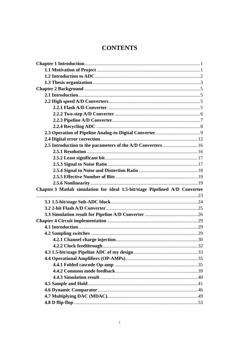
CONTENTS
Chapter 1 Introduction................................................................................................1 1.1 Motivation of Project ......................................................................................1 1.2 Introduction to ADC .......................................................................................2 1.3 Thesis organization .........................................................................................3
Chapter 2 Background ................................................................................................5 2.1 Introduction.....................................................................................................5 2.2 High speed A/D Converters............................................................................5
2.2.1 Flash A/D Converter .............................................................................5 2.2.2 Two-step A/D Converter .......................................................................6 2.2.3 Pipeline A/D Converter.........................................................................7 2.2.4 Recycling ADC ......................................................................................8
2.3 Operation of Pipeline Analog-to-Digital Converter.....................................9 2.4 Digital error correction.................................................................................12 2.5 Introduction to the parameters of the A/D Converters .............................16
2.5.1 Resolution ............................................................................................16 2.5.2 Least significant bit.............................................................................17 2.5.3 Signal to Noise Ratio...........................................................................17 2.5.4 Signal to Noise and Distortion Ratio .................................................18 2.5.5 Effective Number of Bits ....................................................................19 2.5.6 Nonlinearity .........................................................................................19
Chapter 3 Matlab simulation for ideal 1.5-bit/stage Pipelined A/D Converter......................................................................................................................................23
3.1 1.5-bit/stage Sub-ADC block........................................................................24 3.2 2-bit Flash A/D Converter ............................................................................25 3.3 Simulation result for Pipeline A/D Converter ............................................26
Chapter 4 Circuit implementation ...........................................................................29 4.1 Introduction...................................................................................................29 4.2 Sampling switches .........................................................................................29
4.2.1 Channel charge injection....................................................................30 4.2.2 Clock feedthrough...............................................................................32
4.3 1.5-bit/stage Pipeline ADC of my design .....................................................33 4.4 Operational Amplifiers (OP-AMPs)............................................................35
4.4.1 Folded cascode Op-amp .....................................................................35 4.4.2 Common mode feedback ....................................................................39 4.4.3 Simulation result .................................................................................40
4.5 Sample and Hold ...........................................................................................41 4.6 Dynamic Comparator ...................................................................................46 4.7 Multiplying DAC (MDAC)...........................................................................49 4.8 D flip-flop .......................................................................................................53

ii
4.9 Digital error correction.................................................................................54 4.10 noise analysis ...............................................................................................55
Chapter 5 Simulation results ....................................................................................61 Chapter 6 Conclusion and Future work ..................................................................65 References ...................................................................................................................67
1
Chapter 1
Introduction
1.1 Motivation of Project
In reality, we know that Digital signal has the advantages of easier processing,
analysis and storage. So we convert the analog signal to the digital signal for
processing. The way to realize this is that we can use the analog to digital converter as
the interface. Take Optical Mouse for a simple example, when the radiation
component delivers the light to the desktop, then it is reflected. Finally it’s detected by
the Image Sensor. At this moment, output voltage will be generated according to the
intensity of reflected light. This kind of output voltage is analog signal. Then ADC is
used to convert this signal to digital signal which can be processed by DSP.
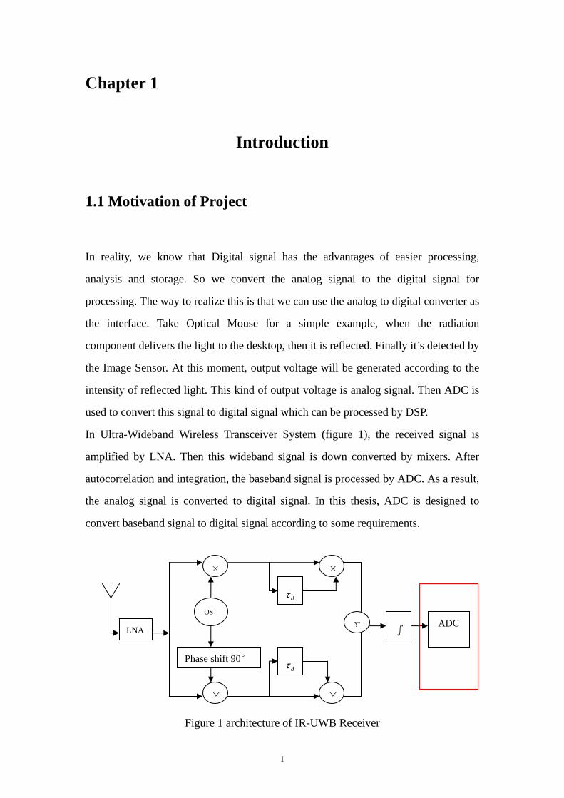
In Ultra-Wideband Wireless Transceiver System (figure 1), the received signal is
amplified by LNA. Then this wideband signal is down converted by mixers. After
autocorrelation and integration, the baseband signal is processed by ADC. As a result,
the analog signal is converted to digital signal. In this thesis, ADC is designed to
convert baseband signal to digital signal according to some requirements.
Figure 1 architecture of IR-UWB Receiver
LNA
×
×
OS
Phase shift 90°
dτ
dτ
×
×
∑∫ ADC
2
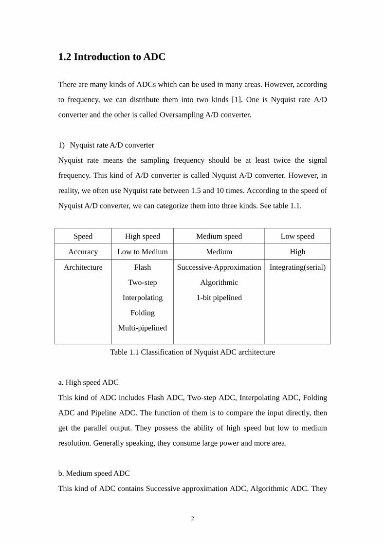
1.2 Introduction to ADC There are many kinds of ADCs which can be used in many areas. However, according
to frequency, we can distribute them into two kinds [1]. One is Nyquist rate A/D
converter and the other is called Oversampling A/D converter.
1) Nyquist rate A/D converter
Nyquist rate means the sampling frequency should be at least twice the signal
frequency. This kind of A/D converter is called Nyquist A/D converter. However, in
reality, we often use Nyquist rate between 1.5 and 10 times. According to the speed of
Nyquist A/D converter, we can categorize them into three kinds. See table 1.1.
Speed High speed Medium speed Low speed
Accuracy Low to Medium Medium High
Architecture Flash
Two-step
Interpolating
Folding
Multi-pipelined
Successive-Approximation
Algorithmic
1-bit pipelined
Integrating(serial)
Table 1.1 Classification of Nyquist ADC architecture
a. High speed ADC
This kind of ADC includes Flash ADC, Two-step ADC, Interpolating ADC, Folding
ADC and Pipeline ADC. The function of them is to compare the input directly, then
get the parallel output. They possess the ability of high speed but low to medium
resolution. Generally speaking, they consume large power and more area.
b. Medium speed ADC
This kind of ADC contains Successive approximation ADC, Algorithmic ADC. They
3
use the method dividing by 2 in each level to find out the corresponding position
where the output is. The speed of these is about tens of KHz to hundred KHz.
c. Low speed ADC
This kind of ADC, such as Integrating ADC, has the low speed but high resolution,
which can be used to process the requirements of high resolution but slow changeable
signals.
2) Oversampling A/D Converter
Oversampling A/D converter can also be called Sigma-Delta A/D converter. It uses
the idea of Noise shaping and Oversampling frequency technology to improve the
Signal to Noise Ratio (SNR), then to increase the resolution.
1.3 Thesis organization
In this thesis, Pipeline ADC was designed by 4bit resolution and 250MHz sampling
speed. Because the frequency of input signal was 100MHz, the sampling frequency
was chosen to be 250MHz considering safe margin and Nyquist-rate. Resolution was
defined by positioning of the waveform. The content of thesis can be divided into 6
chapters, which can be seen as follows.
Chapter 1 it gives purpose of thesis and short introduction to ADC.
Chapter 2 it introduces several types of high speed ADCs and gives an abstract
description of pipeline ADC. At last some parameters of ADCs are presented.
Chapter 3 it presents the simulation of ideal case 1.5-bit per stage Pipeline ADC and
gives a short explanation of each block.
Chapter 4 it is the main part of thesis and discusses circuit implementation of every
block separately and presents some analysis of noise.
Chapter 5 it gives the simulation results.
Chapter 6 it contains the conclusion and future work.

4
5
Chapter 2
Background
2.1 Introduction
In this chapter, I will present several types of high speed ADCs. Namely, Flash ADC,
Two-step ADC, Pipeline ADC, Recycling ADC. Advantages and disadvantages will
be shown in each type. After this, the work operation of Pipeline ADC, introduction of
digital error correction and some of parameters of ADCs will be discussed.
2.2 High speed A/D Converters
2.2.1 Flash A/D Converter
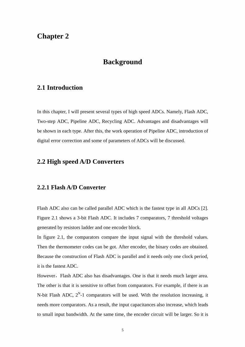
Flash ADC also can be called parallel ADC which is the fastest type in all ADCs [2].
Figure 2.1 shows a 3-bit Flash ADC. It includes 7 comparators, 7 threshold voltages
generated by resistors ladder and one encoder block.
In figure 2.1, the comparators compare the input signal with the threshold values.
Then the thermometer codes can be got. After encoder, the binary codes are obtained.
Because the construction of Flash ADC is parallel and it needs only one clock period,
it is the fastest ADC.
However,Flash ADC also has disadvantages. One is that it needs much larger area.
The other is that it is sensitive to offset from comparators. For example, if there is an
N-bit Flash ADC, 2N-1 comparators will be used. With the resolution increasing, it
needs more comparators. As a result, the input capacitances also increase, which leads
to small input bandwidth. At the same time, the encoder circuit will be larger. So it is
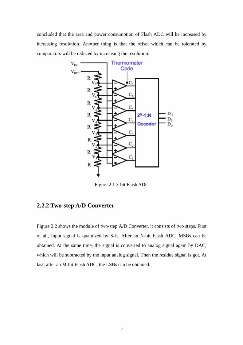
6
concluded that the area and power consumption of Flash ADC will be increased by
increasing resolution. Another thing is that the offset which can be tolerated by
comparators will be reduced by increasing the resolution.
Figure 2.1 3-bit Flash ADC
2.2.2 Two-step A/D Converter
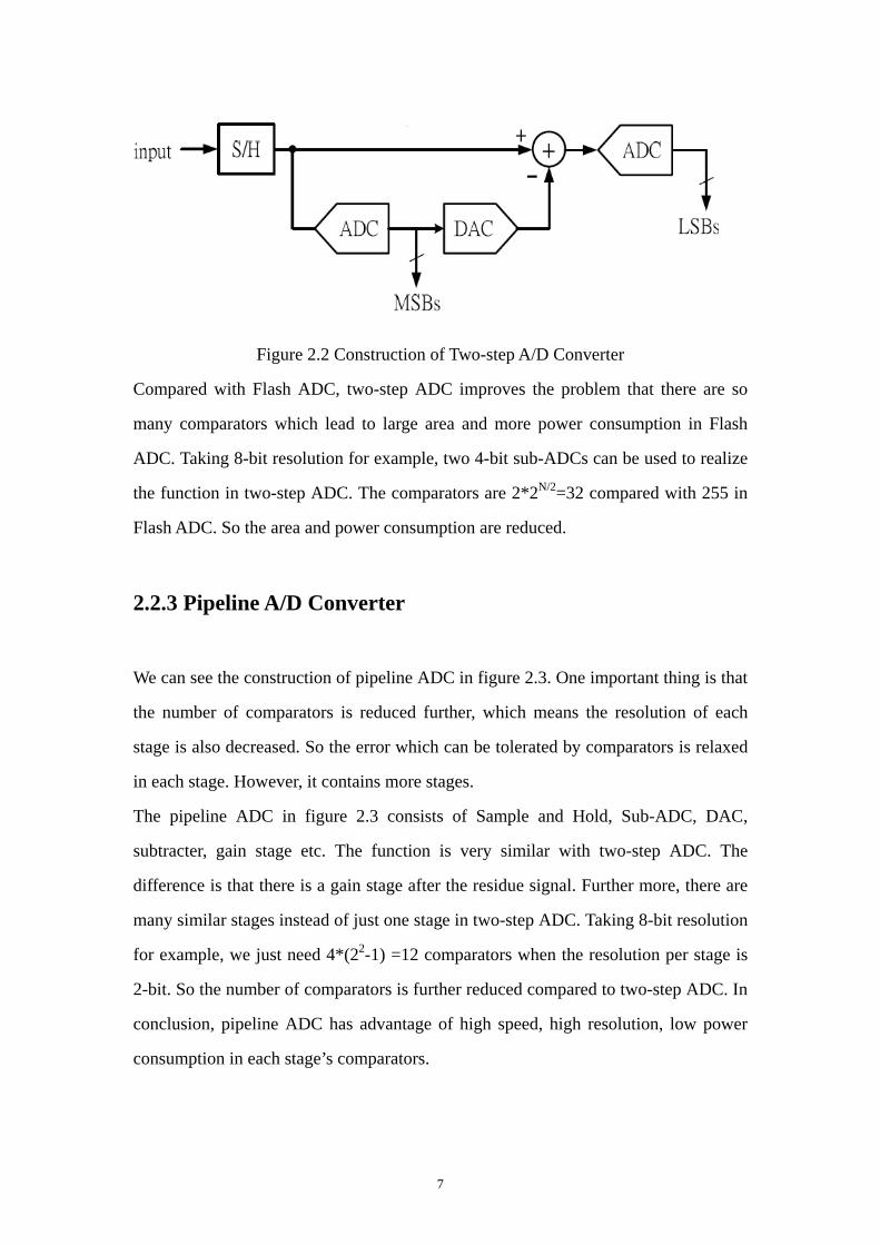
Figure 2.2 shows the module of two-step A/D Converter. it consists of two steps. First
of all, Input signal is quantized by S/H. After an N-bit Flash ADC, MSBs can be
obtained. At the same time, the signal is converted to analog signal again by DAC,
which will be subtracted by the input analog signal. Then the residue signal is got. At
last, after an M-bit Flash ADC, the LSBs can be obtained.
7
Figure 2.2 Construction of Two-step A/D Converter
Compared with Flash ADC, two-step ADC improves the problem that there are so
many comparators which lead to large area and more power consumption in Flash
ADC. Taking 8-bit resolution for example, two 4-bit sub-ADCs can be used to realize
the function in two-step ADC. The comparators are 2*2N/2=32 compared with 255 in
Flash ADC. So the area and power consumption are reduced.
2.2.3 Pipeline A/D Converter
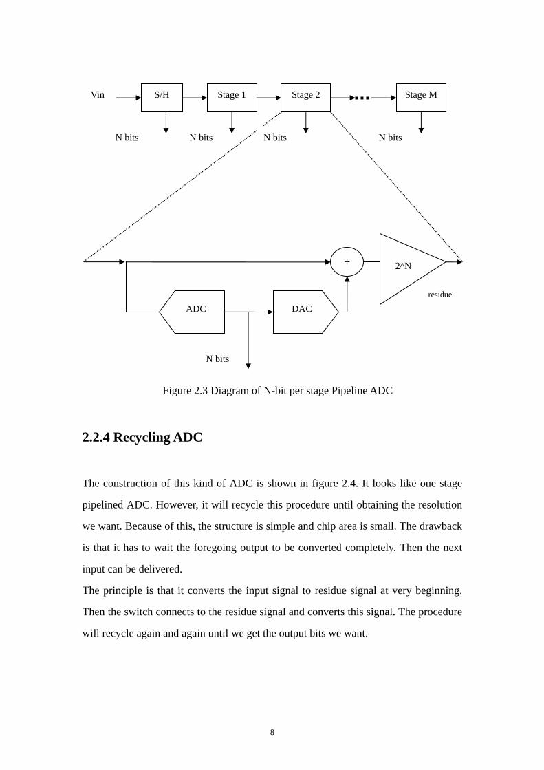
We can see the construction of pipeline ADC in figure 2.3. One important thing is that
the number of comparators is reduced further, which means the resolution of each
stage is also decreased. So the error which can be tolerated by comparators is relaxed
in each stage. However, it contains more stages.
The pipeline ADC in figure 2.3 consists of Sample and Hold, Sub-ADC, DAC,
subtracter, gain stage etc. The function is very similar with two-step ADC. The
difference is that there is a gain stage after the residue signal. Further more, there are
many similar stages instead of just one stage in two-step ADC. Taking 8-bit resolution
for example, we just need 4*(22-1) =12 comparators when the resolution per stage is
2-bit. So the number of comparators is further reduced compared to two-step ADC. In
conclusion, pipeline ADC has advantage of high speed, high resolution, low power
consumption in each stage’s comparators.
8
Figure 2.3 Diagram of N-bit per stage Pipeline ADC
2.2.4 Recycling ADC
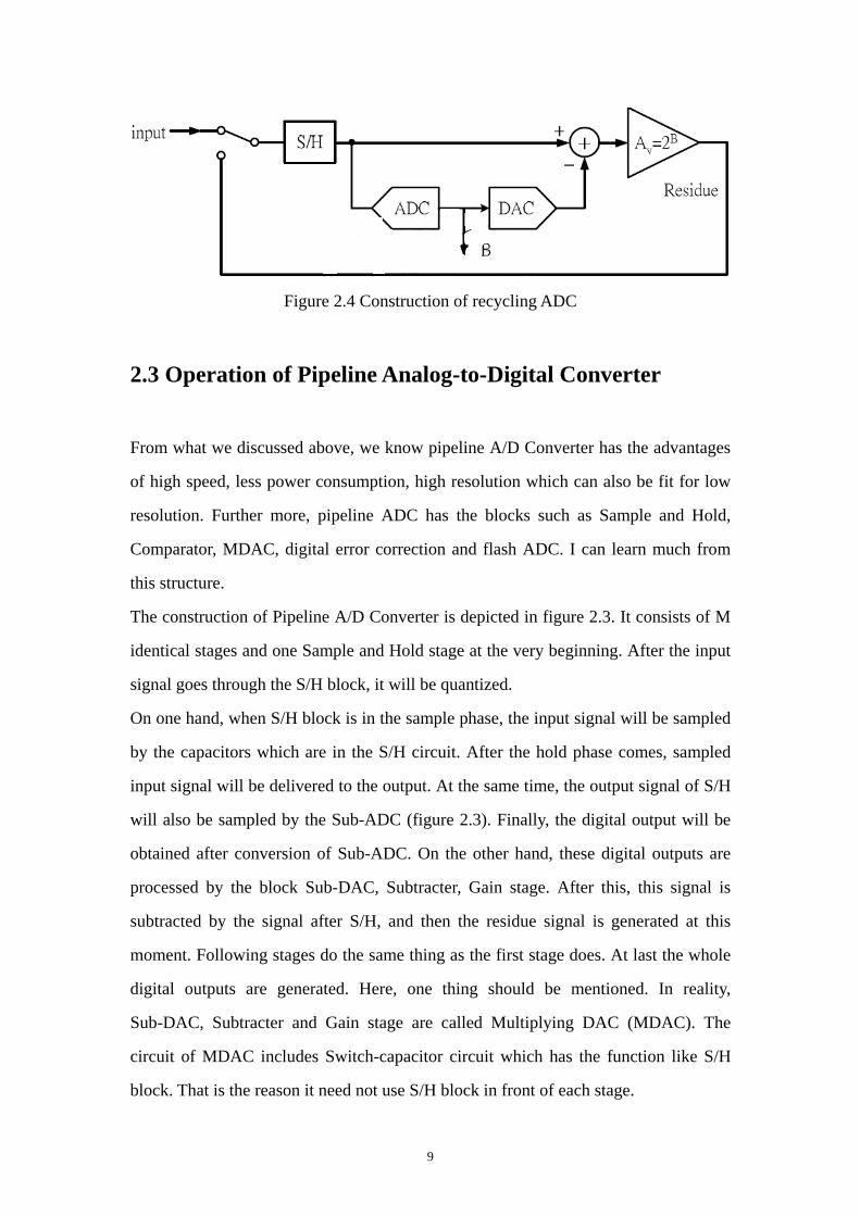
The construction of this kind of ADC is shown in figure 2.4. It looks like one stage
pipelined ADC. However, it will recycle this procedure until obtaining the resolution
we want. Because of this, the structure is simple and chip area is small. The drawback
is that it has to wait the foregoing output to be converted completely. Then the next
input can be delivered.
The principle is that it converts the input signal to residue signal at very beginning.
Then the switch connects to the residue signal and converts this signal. The procedure
will recycle again and again until we get the output bits we want.
Vin S/H Stage 1 Stage 2 Stage M
N bits N bits N bits N bits
ADC DAC
+ 2^N
N bits
residue
9
Figure 2.4 Construction of recycling ADC
2.3 Operation of Pipeline Analog-to-Digital Converter
From what we discussed above, we know pipeline A/D Converter has the advantages
of high speed, less power consumption, high resolution which can also be fit for low
resolution. Further more, pipeline ADC has the blocks such as Sample and Hold,
Comparator, MDAC, digital error correction and flash ADC. I can learn much from
this structure.
The construction of Pipeline A/D Converter is depicted in figure 2.3. It consists of M
identical stages and one Sample and Hold stage at the very beginning. After the input
signal goes through the S/H block, it will be quantized.
On one hand, when S/H block is in the sample phase, the input signal will be sampled
by the capacitors which are in the S/H circuit. After the hold phase comes, sampled
input signal will be delivered to the output. At the same time, the output signal of S/H
will also be sampled by the Sub-ADC (figure 2.3). Finally, the digital output will be
obtained after conversion of Sub-ADC. On the other hand, these digital outputs are
processed by the block Sub-DAC, Subtracter, Gain stage. After this, this signal is
subtracted by the signal after S/H, and then the residue signal is generated at this
moment. Following stages do the same thing as the first stage does. At last the whole
digital outputs are generated. Here, one thing should be mentioned. In reality,
Sub-DAC, Subtracter and Gain stage are called Multiplying DAC (MDAC). The
circuit of MDAC includes Switch-capacitor circuit which has the function like S/H
block. That is the reason it need not use S/H block in front of each stage.
10
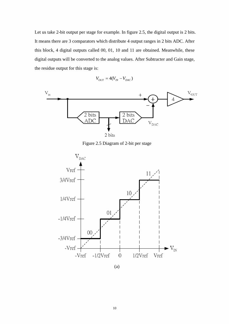
Let us take 2-bit output per stage for example. In figure 2.5, the digital output is 2 bits.
It means there are 3 comparators which distribute 4 output ranges in 2 bits ADC. After
this block, 4 digital outputs called 00, 01, 10 and 11 are obtained. Meanwhile, these
digital outputs will be converted to the analog values. After Subtracter and Gain stage,
the residue output for this stage is:
4( )OUT IN DACV V V= −
Figure 2.5 Diagram of 2-bit per stage
(a)
11
(b)
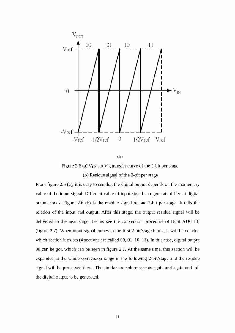
Figure 2.6 (a) VDAC to VIN transfer curve of the 2-bit per stage
(b) Residue signal of the 2-bit per stage
From figure 2.6 (a), it is easy to see that the digital output depends on the momentary
value of the input signal. Different value of input signal can generate different digital
output codes. Figure 2.6 (b) is the residue signal of one 2-bit per stage. It tells the
relation of the input and output. After this stage, the output residue signal will be
delivered to the next stage. Let us see the conversion procedure of 8-bit ADC [3]
(figure 2.7). When input signal comes to the first 2-bit/stage block, it will be decided
which section it exists (4 sections are called 00, 01, 10, 11). In this case, digital output
00 can be got, which can be seen in figure 2.7. At the same time, this section will be
expanded to the whole conversion range in the following 2-bit/stage and the residue
signal will be processed there. The similar procedure repeats again and again until all
the digital output to be generated.
12
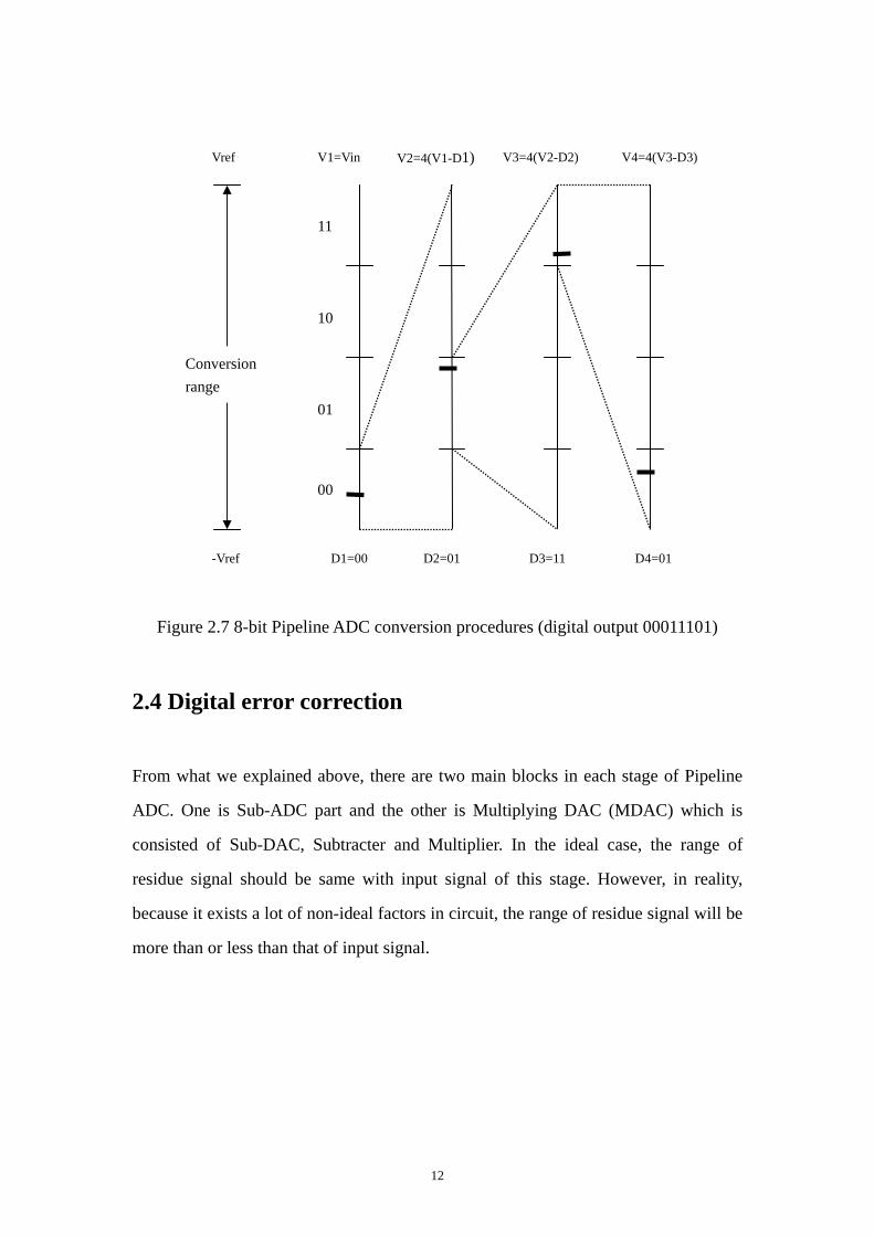
Figure 2.7 8-bit Pipeline ADC conversion procedures (digital output 00011101)
2.4 Digital error correction
From what we explained above, there are two main blocks in each stage of Pipeline
ADC. One is Sub-ADC part and the other is Multiplying DAC (MDAC) which is
consisted of Sub-DAC, Subtracter and Multiplier. In the ideal case, the range of
residue signal should be same with input signal of this stage. However, in reality,
because it exists a lot of non-ideal factors in circuit, the range of residue signal will be
more than or less than that of input signal.
11
10
01
00
V3=4(V2-D2) V4=4(V3-D3)
D1=00 D2=01 D3=11 D4=01
Conversion range
-Vref
Vref V2=4(V1-D1)V1=Vin
13
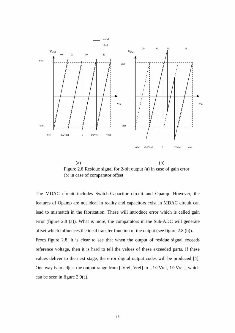
The MDAC circuit includes Switch-Capacitor circuit and Opamp. However, the
features of Opamp are not ideal in reality and capacitors exist in MDAC circuit can
lead to mismatch in the fabrication. These will introduce error which is called gain
error (figure 2.8 (a)). What is more, the comparators in the Sub-ADC will generate
offset which influences the ideal transfer function of the output (see figure 2.8 (b)).
From figure 2.8, it is clear to see that when the output of residue signal exceeds
reference voltage, then it is hard to tell the values of these exceeded parts. If these
values deliver to the next stage, the error digital output codes will be produced [4].
One way is to adjust the output range from [-Vref, Vref] to [-1/2Vref, 1/2Vref], which
can be seen in figure 2.9(a).
Vref
-Vref
Vin
Vout Vout
Vref
-Vref
Vin
00 01 10 11
-Vref -1/2Vref 0 1/2Vref Vref
00 01 10 11
-Vref -1/2Vref 0 1/2Vref Vref
actual
ideal
(a) (b) Figure 2.8 Residue signal for 2-bit output (a) in case of gain error (b) in case of comparator offset
14
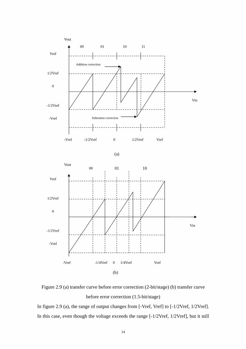
Figure 2.9 (a) transfer curve before error correction (2-bit/stage) (b) transfer curve
before error correction (1.5-bit/stage)
In figure 2.9 (a), the range of output changes from [-Vref, Vref] to [-1/2Vref, 1/2Vref].
In this case, even though the voltage exceeds the range [-1/2Vref, 1/2Vref], but it still
(b)
Vref
1/2Vref
0
-1/2Vref
-Vref
Vref
1/2Vref
0
-1/2Vref
-Vref
-Vref -1/2Vref 0 1/2Vref Vref
Vin
Vout
00 01 10 11
Vin
Vout
-Vref -1/4Vref 0 1/4Vref Vref
00 01 10
(a)
Addition correction
Subtration correction
15
in the range [-Vref, Vref]. So the method that the output code of next stage plus or
subtracts the output code of this stage can be used. Finally the correct output codes
can be got. This method using one bit output code of this stage plus/subtracts one bit
output code of next stage is called digital error correction [5] [6].
Figure 2.9 (b) is the result when the curve in figure 2.9 (a) moves 0.5 LSB to the
positive direction of Vin axis and neglects the most right part curve. In this case, only
addition correction need to be done and the complexity of the circuit will be further
reduced. Using this method, the digital outputs of 1.5-bit/stage are 00, 01 and 10.
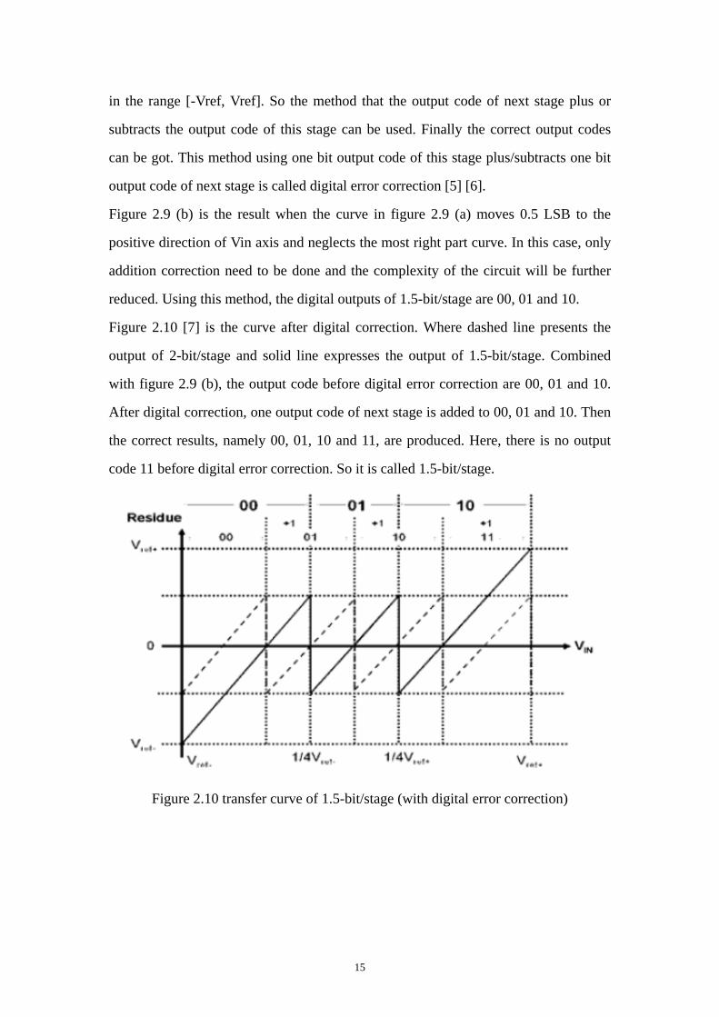
Figure 2.10 [7] is the curve after digital correction. Where dashed line presents the
output of 2-bit/stage and solid line expresses the output of 1.5-bit/stage. Combined
with figure 2.9 (b), the output code before digital error correction are 00, 01 and 10.
After digital correction, one output code of next stage is added to 00, 01 and 10. Then
the correct results, namely 00, 01, 10 and 11, are produced. Here, there is no output
code 11 before digital error correction. So it is called 1.5-bit/stage.
Figure 2.10 transfer curve of 1.5-bit/stage (with digital error correction)
16
2 bits/stage 1.5 bits/stage
Input range [-Vref, Vref] [-Vref, Vref]
Sub-ADC threshold levels -1/2Vref, 0, 1/2Vref -1/4Vref, 1/4Vref
Comparator numbers/stage 3 2
Digital codes 00, 01, 10, 11 00, 01, 10
Stage gain 4 2
Bits/stage 2 1.5
Table 2.1 comparison between 1.5-bit/stage and 2-bit/stage
In table 2.1, it is listed parameters between 1.5-bit/stage and 2-bit/stage. It is obvious
that the comparators in 1.5-bit/stage are one less than those in 2-bit/stage. So the gain
is also reduced by 2. In this case, 1.5-bit/stage has less chip area and less power
consumption than that of 2-bit/stage.
2.5 Introduction to the parameters of the A/D Converters
There are a lot of parameters of A/D Converters. Different parameters correspond to
different requirements. Here, I will introduce some important parameters in the A/D
Converters.
2.5.1 Resolution Resolution means the number of discrete values ADC can produce. Taking N bits
resolution for example, it represents there are 2N levels can generate in the range of
input signal. If N=8, it means there are 256 levels according to the input range. In
reality, the resolution we get from ADC is a measurement result. It is called Effective
Number of Bits (ENOB) which will be explained later.
17
2.5.2 Least significant bit
Generally speaking, least significant bit can be represented as voltage which is called
the least significant voltage. It means the minimum voltage can be obtained according
to the input voltage. Or we can also say that the digital output can be converted to the
next step after one least significant voltage.
Let us take 10-bit ADC for example. If we assume input voltage is from -1V to +1V.
Then the least significant voltage can be calculated as,
( )
2ref ref
LSB N
V VV + −−
= (2.1)
From equation 2.1, we know that ( )10
1 ( 1)1.953125
2LSBV mV− −
= = which means one
LSB= 1.953125mV.
2.5.3 Signal to Noise Ratio
Signal to noise ratio means the power ratio between signal and noise. The unit is dB.
If this value is large, it represents that signal will be less influenced by noise and
better performance will be.
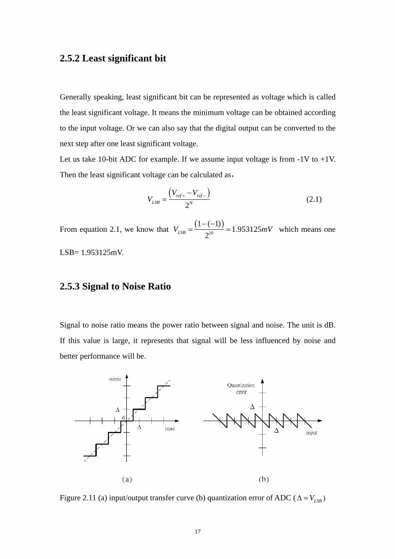
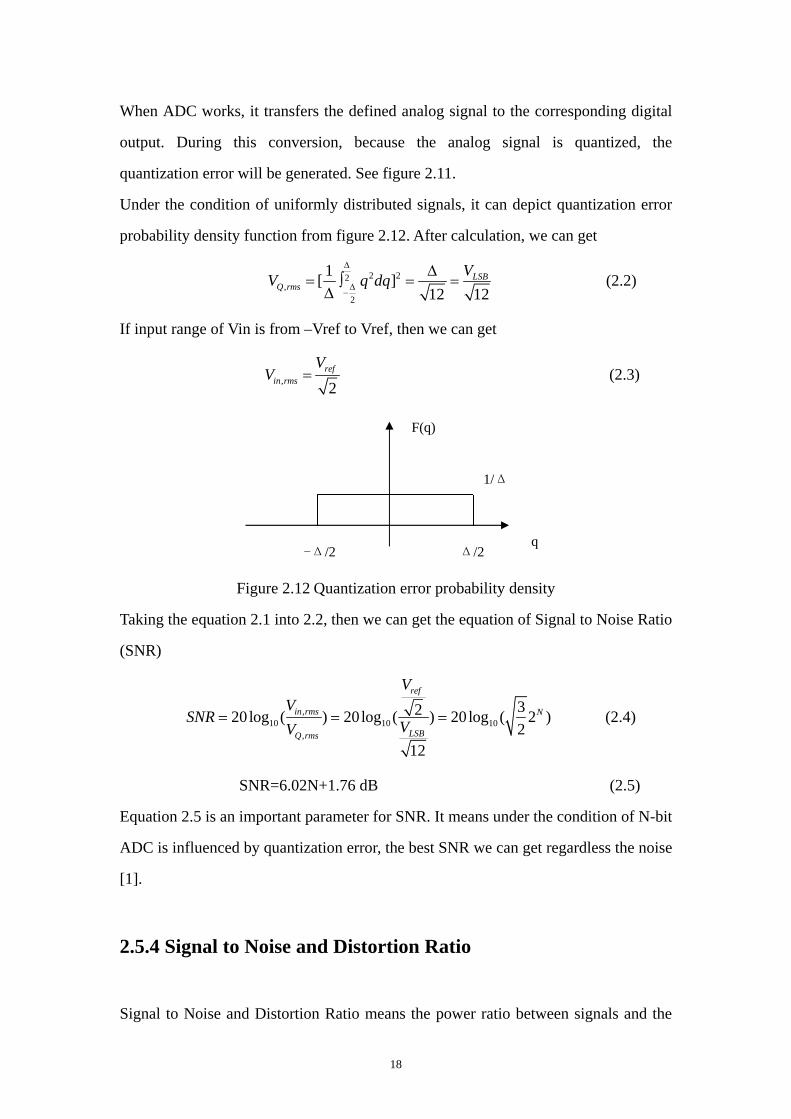
Figure 2.11 (a) input/output transfer curve (b) quantization error of ADC ( LSBVΔ = )
18
When ADC works, it transfers the defined analog signal to the corresponding digital
output. During this conversion, because the analog signal is quantized, the
quantization error will be generated. See figure 2.11.
Under the condition of uniformly distributed signals, it can depict quantization error
probability density function from figure 2.12. After calculation, we can get
2 22,
2
1[ ]12 12
LSBQ rms
VV q dqΔ
Δ−
Δ= ∫ = =
Δ (2.2)
If input range of Vin is from –Vref to Vref, then we can get
, 2ref
in rms
VV = (2.3)
Figure 2.12 Quantization error probability density
Taking the equation 2.1 into 2.2, then we can get the equation of Signal to Noise Ratio
(SNR)
,10 10 10
,
3220log ( ) 20log ( ) 20log ( 2 )2
12
ref
in rms N
LSBQ rms
VV
SNR VV= = = (2.4)
SNR=6.02N+1.76 dB (2.5)
Equation 2.5 is an important parameter for SNR. It means under the condition of N-bit
ADC is influenced by quantization error, the best SNR we can get regardless the noise
[1].
2.5.4 Signal to Noise and Distortion Ratio
Signal to Noise and Distortion Ratio means the power ratio between signals and the
-Δ/2 Δ/2 q
F(q)
1/Δ
19
summation of noise and total harmonic distortion. The unit is dB. It represents how
much noise and distortion can influence the signals. SNDR is also the value to
calculate the effective number of bits.
2.5.5 Effective Number of Bits
In reality, the output signals contain the real signals we want, noise and harmonic
distortion signals. So the resolution we get does not equal to the ideal case resolution.
That is the reason why we define ENOB to denote the real resolution after ADC.
The expression can be written as follows
1.76
6.02peakSNDR
ENOB−
= (2.6)
2.5.6 Nonlinearity
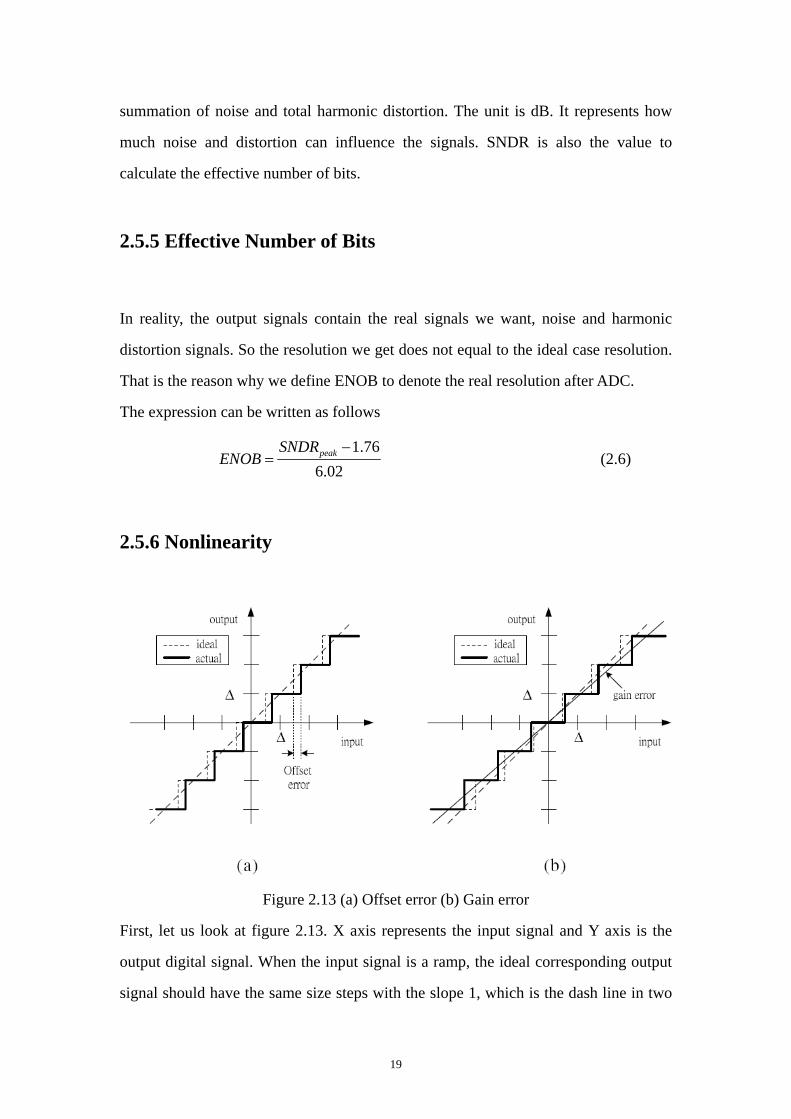
Figure 2.13 (a) Offset error (b) Gain error
First, let us look at figure 2.13. X axis represents the input signal and Y axis is the
output digital signal. When the input signal is a ramp, the ideal corresponding output
signal should have the same size steps with the slope 1, which is the dash line in two
20
figures. However, in real A/D Converter circuit, every circuit element will generate
nonlinear effect which leads to the steps are not so perfect. In figure 2.13 (a), it is the
offset error which leads to the drift of the output signals. In figure 2.13 (b), it is the
gain error which makes the output steps have different size.
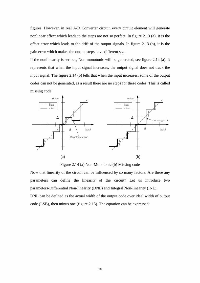
If the nonlinearity is serious, Non-monotonic will be generated, see figure 2.14 (a). It
represents that when the input signal increases, the output signal does not track the
input signal. The figure 2.14 (b) tells that when the input increases, some of the output
codes can not be generated, as a result there are no steps for these codes. This is called
missing code.
(a) (b)
Figure 2.14 (a) Non-Monotonic (b) Missing code
Now that linearity of the circuit can be influenced by so many factors. Are there any
parameters can define the linearity of the circuit? Let us introduce two
parameters-Differential Non-linearity (DNL) and Integral Non-linearity (INL).
DNL can be defined as the actual width of the output code over ideal width of output
code (LSB), then minus one (figure 2.15). The equation can be expressed:
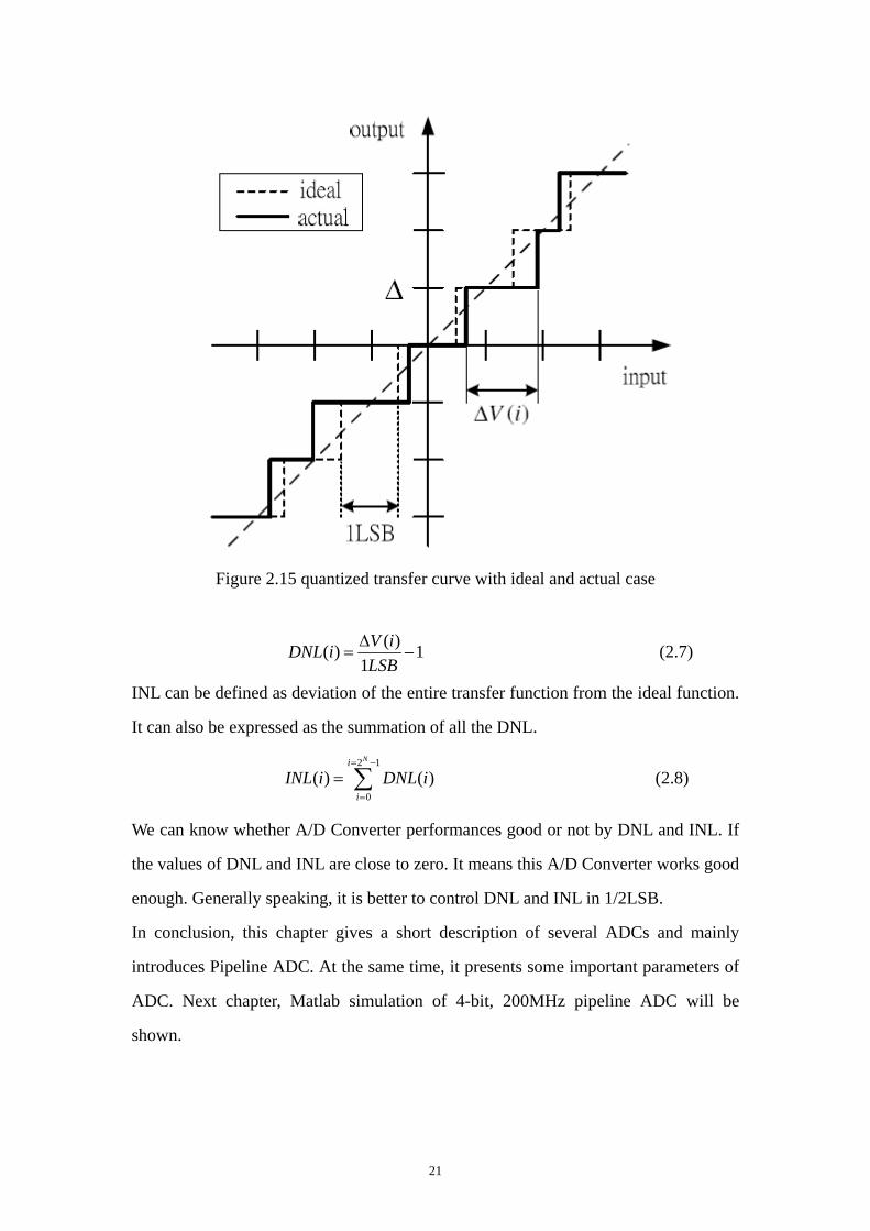
21
Figure 2.15 quantized transfer curve with ideal and actual case
( )( ) 1
1V iDNL iLSBΔ
= − (2.7)
INL can be defined as deviation of the entire transfer function from the ideal function.
It can also be expressed as the summation of all the DNL.
2 1
0( ) ( )
Ni
iINL i DNL i
= −
=
= ∑ (2.8)
We can know whether A/D Converter performances good or not by DNL and INL. If
the values of DNL and INL are close to zero. It means this A/D Converter works good
enough. Generally speaking, it is better to control DNL and INL in 1/2LSB.
In conclusion, this chapter gives a short description of several ADCs and mainly
introduces Pipeline ADC. At the same time, it presents some important parameters of
ADC. Next chapter, Matlab simulation of 4-bit, 200MHz pipeline ADC will be
shown.

22
23
Chapter 3
Matlab simulation for ideal 1.5-bit/stage Pipelined
A/D Converter
In order to have a concept of pipelined A/D Converter and know how it works, the
system level using Matlab was finished. In simulation only ideal case has been done
because of the time limitation.
According to Nyquist rate, sampling speed should be equal to or larger than 200MHz
when input signal is 100MHz. In simulation, sampling speed of 200MHz is chosen
and the resolution is 4 bits.
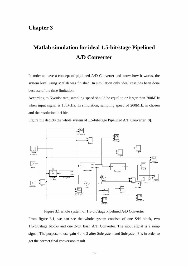
Figure 3.1 depicts the whole system of 1.5-bit/stage Pipelined A/D Converter [8].
Figure 3.1 whole system of 1.5-bit/stage Pipelined A/D Converter
From figure 3.1, we can see the whole system consists of one S/H block, two
1.5-bit/stage blocks and one 2-bit flash A/D Converter. The input signal is a ramp
signal. The purpose to use gain 4 and 2 after Subsystem and Subsystem3 is in order to
get the correct final conversion result.
24
3.1 1.5-bit/stage Sub-ADC block
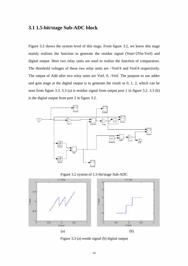
Figure 3.2 shows the system level of this stage. From figure 3.2, we know this stage
mainly realizes the function to generate the residue signal (Vout=2Vin-Vref) and
digital output. Here two relay units are used to realize the function of comparators.
The threshold voltages of these two relay units are –Vref/4 and Vref/4 respectively.
The output of Add after two relay units are Vref, 0, -Vref. The purpose to use adder
and gain stage at the digital output is to generate the result as 0, 1, 2, which can be
seen from figure 3.3. 3.3 (a) is residue signal from output port 1 in figure 3.2. 3.3 (b)
is the digital output from port 2 in figure 3.2.
Figure 3.2 system of 1.5-bit/stage Sub-ADC
(a) (b)
Figure 3.3 (a) reside signal (b) digital output
25
Figure 3.4 shows the result of second stage of 1.5-bit/stage Sub-ADC. 3.4 (a) is the
residue signal and 3.4 (b) is digital output.
Figure 3.4 (a) residue signal (b) digital output
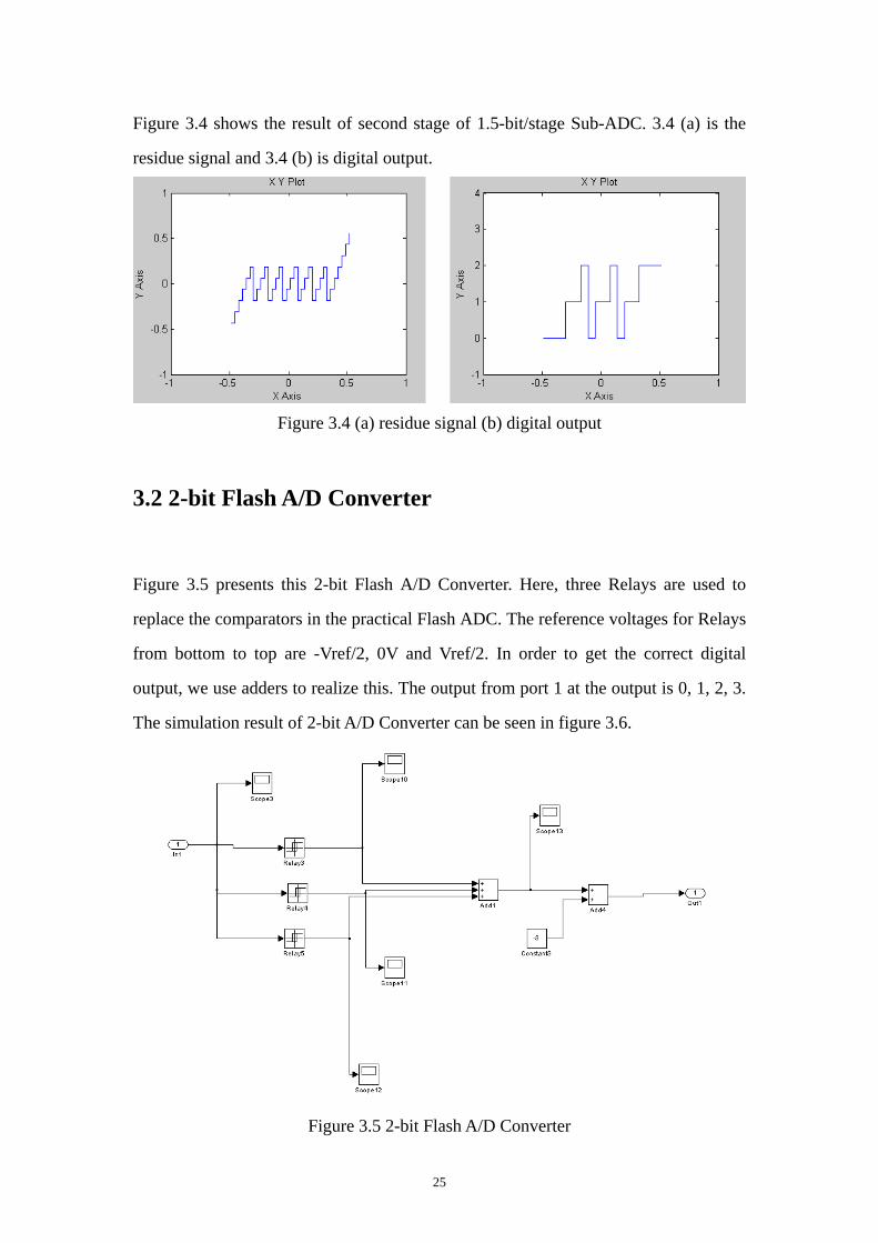
3.2 2-bit Flash A/D Converter
Figure 3.5 presents this 2-bit Flash A/D Converter. Here, three Relays are used to
replace the comparators in the practical Flash ADC. The reference voltages for Relays
from bottom to top are -Vref/2, 0V and Vref/2. In order to get the correct digital
output, we use adders to realize this. The output from port 1 at the output is 0, 1, 2, 3.
The simulation result of 2-bit A/D Converter can be seen in figure 3.6.
Figure 3.5 2-bit Flash A/D Converter
26
Figure 3.6 result of 2-bit Flash A/D Converter
3.3 Simulation result for Pipeline A/D Converter
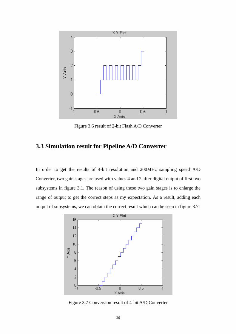
In order to get the results of 4-bit resolution and 200MHz sampling speed A/D
Converter, two gain stages are used with values 4 and 2 after digital output of first two
subsystems in figure 3.1. The reason of using these two gain stages is to enlarge the
range of output to get the correct steps as my expectation. As a result, adding each
output of subsystems, we can obtain the correct result which can be seen in figure 3.7.
Figure 3.7 Conversion result of 4-bit A/D Converter

27
A ramp signal is used as input. From figure 3.7, it is easy to see the ramp signal is
replaced by 16 steps which prove the result correct. After doing this ideal case
simulation on Matlab, I know the whole blocks of my design and have a detailed
concept how to design each block. It is helpful in my future pipeline A/D Converter
circuit design by Cadence.
In conclusion, Chapter 3 presents the whole pipeline ADC simulation structure and
the result. For the next chapter, circuit implementation and results of 4-bit, 250MHz
pipeline ADC will be shown.

28
29
Chapter 4
Circuit implementation
4.1 Introduction
This chapter will introduce all the circuit blocks in my designed Pipeline ADC,
namely OPAMP, S/H, Comparator, MDAC, D flip-flop, Digital Correction circuit.
Each part will be explained in detail and simulation results will also be presented. At
the end of this chapter, noise analysis is shown. In my design, the sampling speed is
250MHz considering safety margin. Resolution is still 4-bit.
4.2 Sampling switches
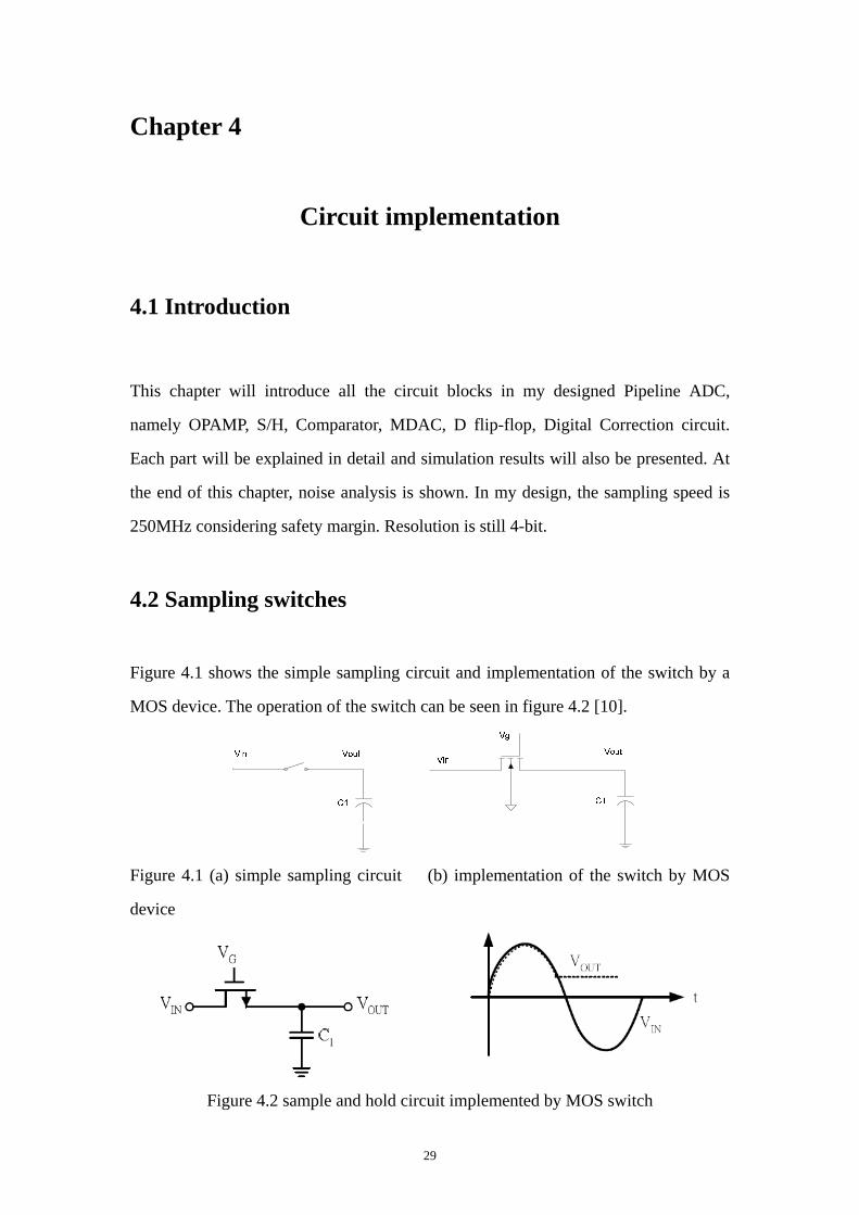
Figure 4.1 shows the simple sampling circuit and implementation of the switch by a
MOS device. The operation of the switch can be seen in figure 4.2 [10].
Figure 4.1 (a) simple sampling circuit (b) implementation of the switch by MOS
device
Figure 4.2 sample and hold circuit implemented by MOS switch
30
The left side of figure 4.2 shows the sample and hold circuit implemented by MOS
switch and the right side of figure 4.2 is the relation between input signal and output
signal. Where the real line is input signal and the dashed line is output signal. When
VG is high, CMOS switch is turned on. Vout follows the track of Vin. When VG is low,
Vout keeps the voltage before the switch turns off. One thing should be mentioned.
When switch is switched on, CMOS works as a resistor. It should satisfy the condition
Vds<<2 (Vgs-Vth). Then:
21 [2( ) ]2d n ox gs th ds ds
WI u C V V V VL
= − − (4.1)
Because Vds is small, the square item of Vds in equation 4.1 can be neglected. The
resistance of switch can be expressed:
1 [2( ) ]2d n ox gs th ds
WI u C V V VL
≈ − (4.2)
1 1( )( )
don
dsn ox gs th
IR WV u C V VL
−∂= =
∂ − (4.3)
From equation 4.3, it is easy to see the resistance of switch is influenced by ratio of
width over length and overdrive voltage.
4.2.1 Channel charge injection
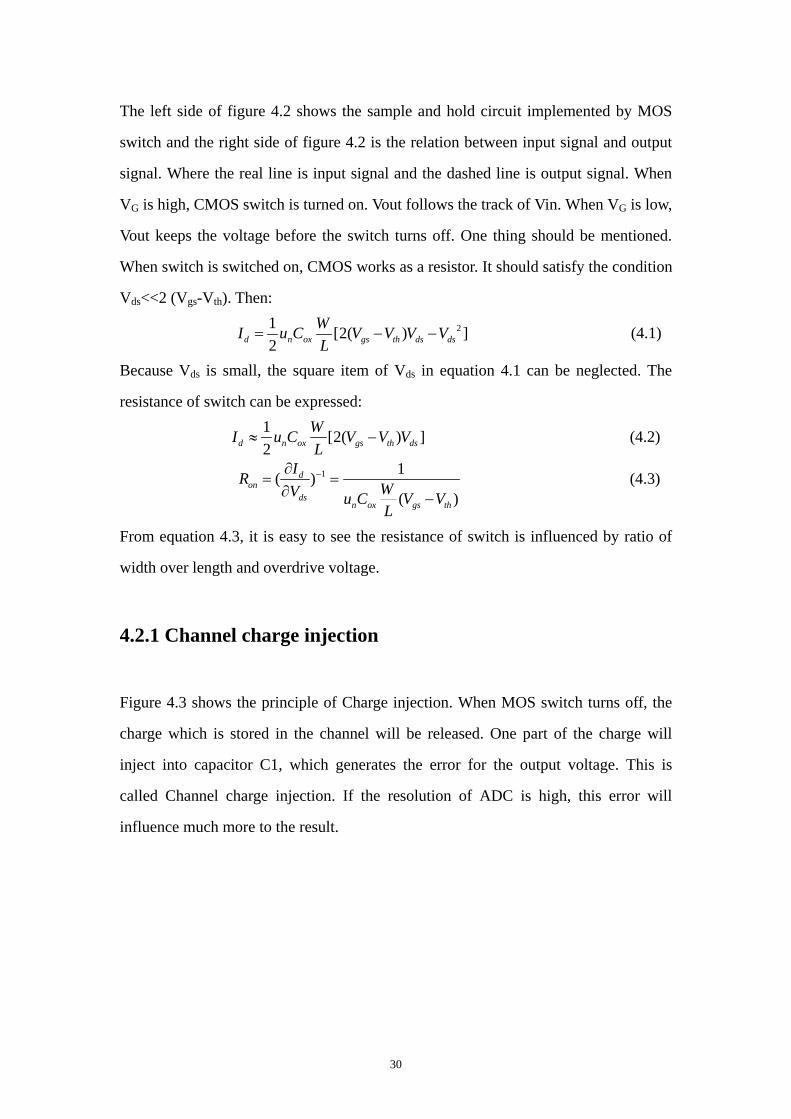
Figure 4.3 shows the principle of Charge injection. When MOS switch turns off, the
charge which is stored in the channel will be released. One part of the charge will
inject into capacitor C1, which generates the error for the output voltage. This is
called Channel charge injection. If the resolution of ADC is high, this error will
influence much more to the result.
31
Figure 4.3 Charge injection
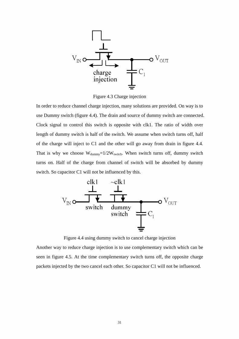
In order to reduce channel charge injection, many solutions are provided. On way is to
use Dummy switch (figure 4.4). The drain and source of dummy switch are connected.
Clock signal to control this switch is opposite with clk1. The ratio of width over
length of dummy switch is half of the switch. We assume when switch turns off, half
of the charge will inject to C1 and the other will go away from drain in figure 4.4.
That is why we choose Wdummy=1/2Wswitch. When switch turns off, dummy switch
turns on. Half of the charge from channel of switch will be absorbed by dummy
switch. So capacitor C1 will not be influenced by this.
Figure 4.4 using dummy switch to cancel charge injection
Another way to reduce charge injection is to use complementary switch which can be
seen in figure 4.5. At the time complementary switch turns off, the opposite charge
packets injected by the two cancel each other. So capacitor C1 will not be influenced.
32
Figure 4.5 using complementary switch to cancel charge injection
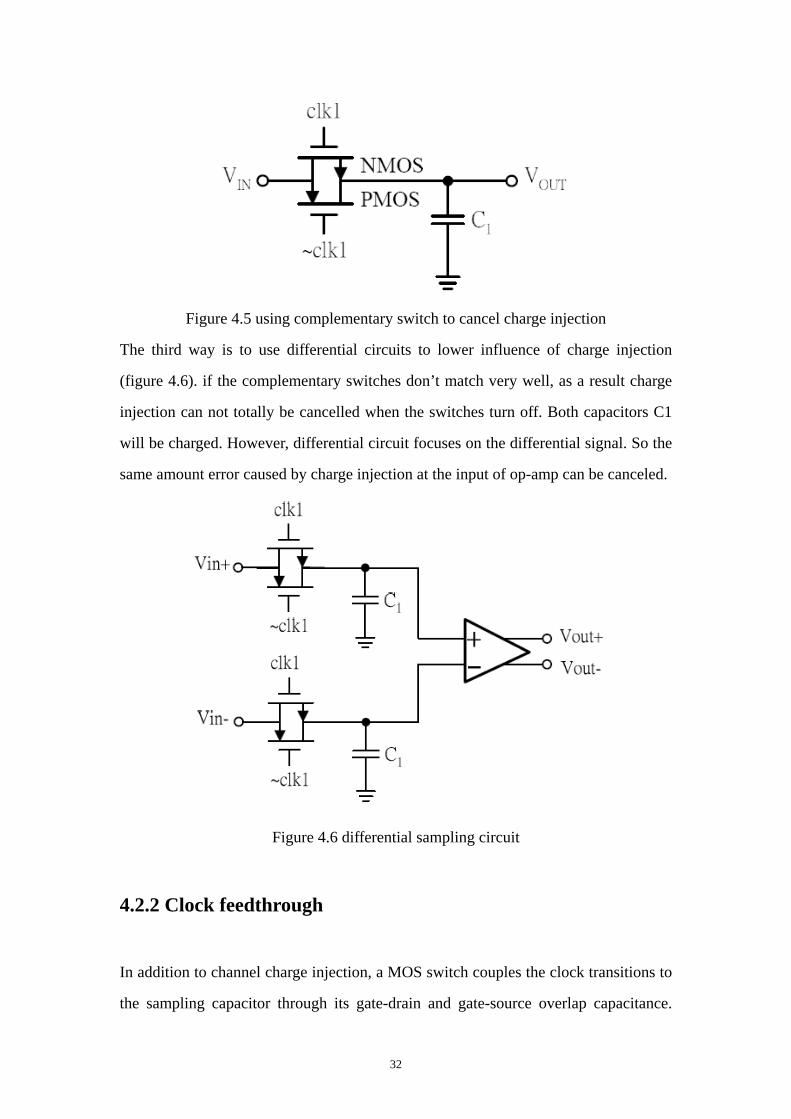
The third way is to use differential circuits to lower influence of charge injection
(figure 4.6). if the complementary switches don’t match very well, as a result charge
injection can not totally be cancelled when the switches turn off. Both capacitors C1
will be charged. However, differential circuit focuses on the differential signal. So the
same amount error caused by charge injection at the input of op-amp can be canceled.
Figure 4.6 differential sampling circuit
4.2.2 Clock feedthrough
In addition to channel charge injection, a MOS switch couples the clock transitions to
the sampling capacitor through its gate-drain and gate-source overlap capacitance.
33
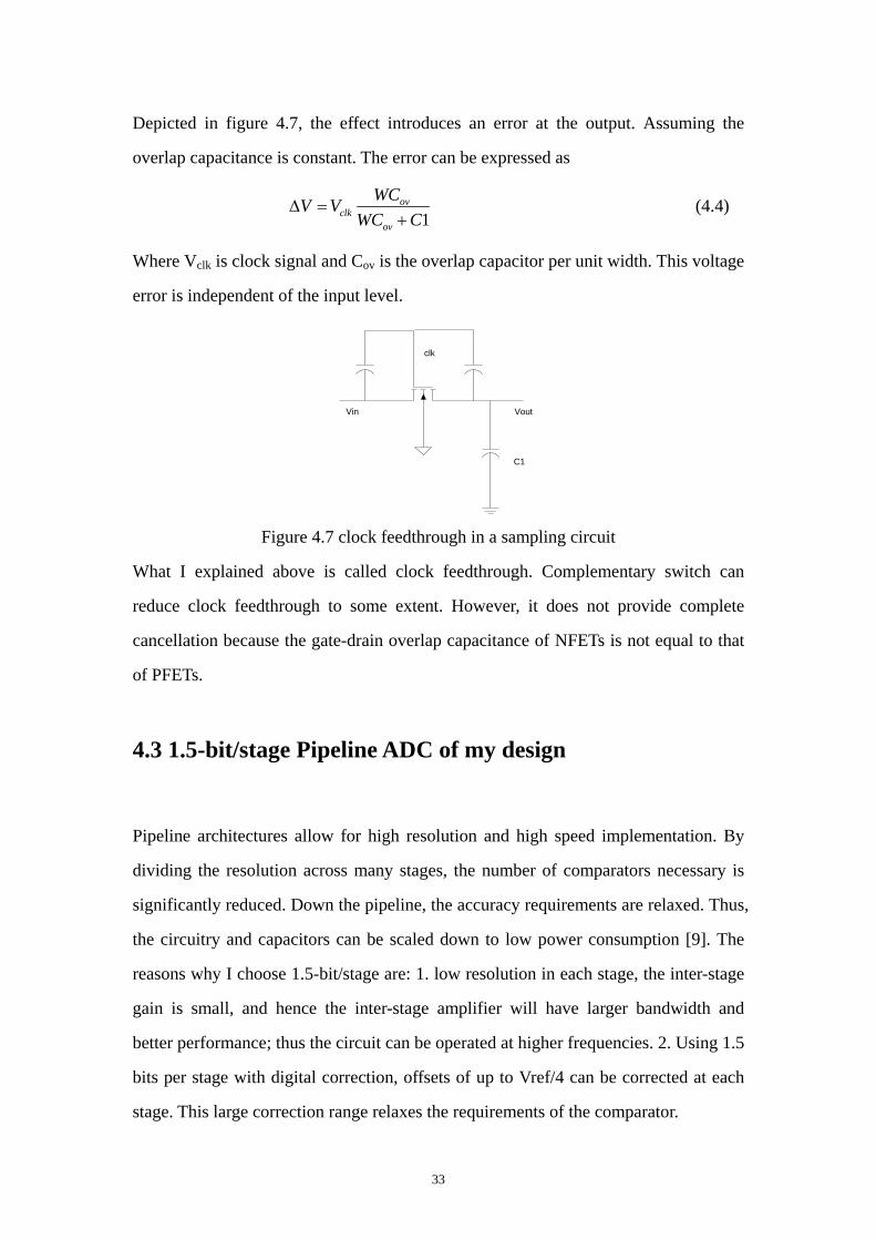
Depicted in figure 4.7, the effect introduces an error at the output. Assuming the
overlap capacitance is constant. The error can be expressed as
1
ovclk
ov
WCV VWC C
Δ =+
(4.4)
Where Vclk is clock signal and Cov is the overlap capacitor per unit width. This voltage
error is independent of the input level.
Vin Vout
C1
clk
Figure 4.7 clock feedthrough in a sampling circuit
What I explained above is called clock feedthrough. Complementary switch can
reduce clock feedthrough to some extent. However, it does not provide complete
cancellation because the gate-drain overlap capacitance of NFETs is not equal to that
of PFETs.
4.3 1.5-bit/stage Pipeline ADC of my design
Pipeline architectures allow for high resolution and high speed implementation. By
dividing the resolution across many stages, the number of comparators necessary is
significantly reduced. Down the pipeline, the accuracy requirements are relaxed. Thus,
the circuitry and capacitors can be scaled down to low power consumption [9]. The
reasons why I choose 1.5-bit/stage are: 1. low resolution in each stage, the inter-stage
gain is small, and hence the inter-stage amplifier will have larger bandwidth and
better performance; thus the circuit can be operated at higher frequencies. 2. Using 1.5
bits per stage with digital correction, offsets of up to Vref/4 can be corrected at each
stage. This large correction range relaxes the requirements of the comparator.
34
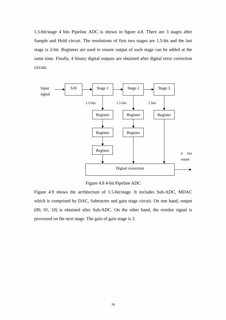
1.5-bit/stage 4 bits Pipeline ADC is shown in figure 4.8. There are 3 stages after
Sample and Hold circuit. The resolutions of first two stages are 1.5-bit and the last
stage is 2-bit. Registers are used to ensure output of each stage can be added at the
same time. Finally, 4 binary digital outputs are obtained after digital error correction
circuit.
Figure 4.8 4-bit Pipeline ADC
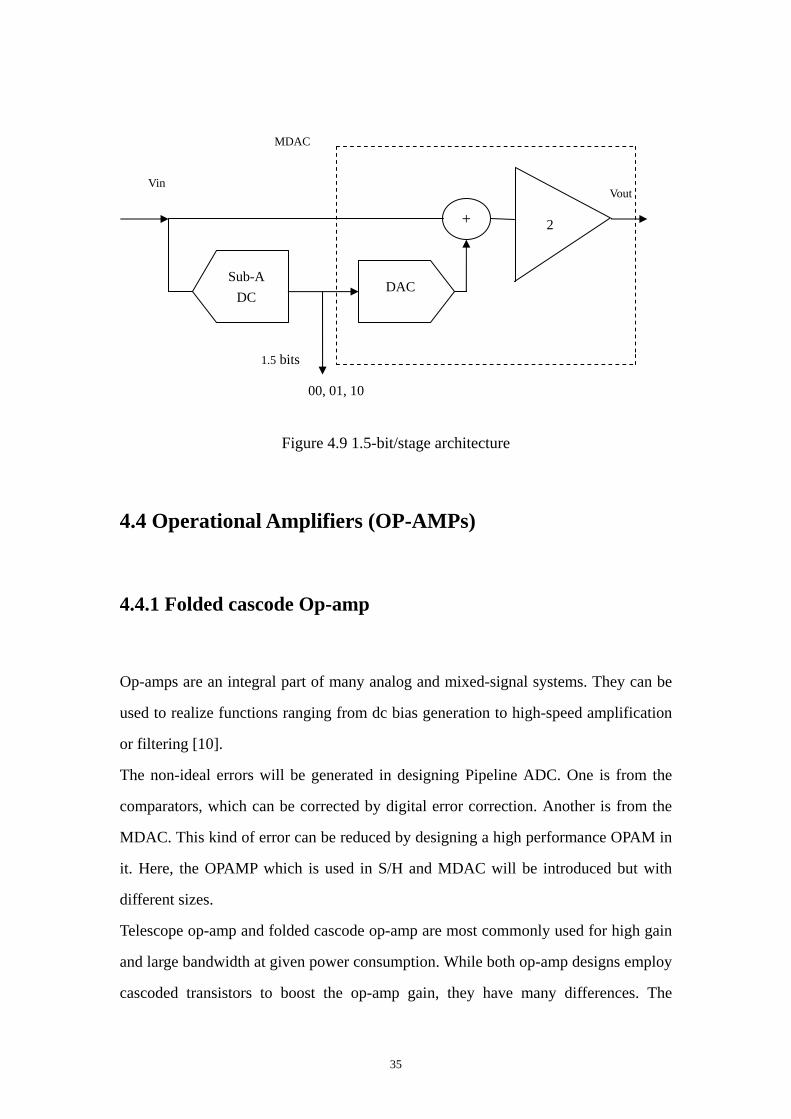
Figure 4.9 shows the architecture of 1.5-bit/stage. It includes Sub-ADC, MDAC
which is comprised by DAC, Subtracter and gain stage circuit. On one hand, output
(00, 01, 10) is obtained after Sub-ADC. On the other hand, the residue signal is
processed on the next stage. The gain of gain stage is 2.
Input signal
S/H Stage 1 Stage 2 Stage 3
Register Register
Register
Digital correction
Register
Register
Register
1.5 bits 1.5 bits 2 bits
4 bits
output
35
Figure 4.9 1.5-bit/stage architecture
4.4 Operational Amplifiers (OP-AMPs)
4.4.1 Folded cascode Op-amp
Op-amps are an integral part of many analog and mixed-signal systems. They can be
used to realize functions ranging from dc bias generation to high-speed amplification
or filtering [10].
The non-ideal errors will be generated in designing Pipeline ADC. One is from the
comparators, which can be corrected by digital error correction. Another is from the
MDAC. This kind of error can be reduced by designing a high performance OPAM in
it. Here, the OPAMP which is used in S/H and MDAC will be introduced but with
different sizes.
Telescope op-amp and folded cascode op-amp are most commonly used for high gain
and large bandwidth at given power consumption. While both op-amp designs employ
cascoded transistors to boost the op-amp gain, they have many differences. The
00, 01, 10
Sub-ADC
DAC
+ 2
1.5 bits
Vin Vout
MDAC
36
telescopic op-amp has the advantages of higher speed and lower power consumption.
But folded cacode op-amp has large output signal swing and large input common
mode range. Considering my supply voltage is only 1.2V and it is easy to control
common mode voltage for folded cascode op-amp. I choose this one.
Firstly, let us get the range of unit gain bandwidth of op-amp. The op-amp’s
closed-loop bandwidth determines the output settling for the S/H. Assuming DC gain
to be large enough, settling error due to op-amp’s finite bandwidth can be written as
[11]:
set
set CL
tt
errV e V e Vωτ− −≈ = (4.5)
Where tset is available settling time, τ is the settling time constant determined by
op-amp’s closed-loop bandwidth CLω . V is op-amp’s ideal output voltage step for
settling. From equation 4.5, we can get the closed-loop bandwidth is (the gain error
for op-amp is 1/27 which comes from the assumption that according to 4-bit ADC, the
accuracy is 1/25, then the accuracy of SHA is 1/26, so 1/27 accuracy for op-amp):
7
9
1( )1 1 4.852 3862 2 2 10
2
CL
Inf MHzTπ π −
−= = =
× (4.6)
Equation 4.6 means the closed-loop bandwidth should be larger than 386MHz. the
relationship between op-amp’s closed-loop bandwidth and op-amp’s unit gain
bandwidth is:
CL UGBf f β= × (4.7)
β in equation 4.7 is feedback factor. The value here is one. So the unit gain
bandwidth should be larger than 386MHz.
Secondly, let us get the range for tail current of op-amp. If considering the worst case,
half the period 2ns is used for Slew rate. When the peak-to-peak input signal is
200mV, Slew Rate should be:
tail
L
ISRC
= (4.8)
Itail is tail current for the input pair of the op-amp. CL is load capacitance. The value
37
for CL is 1.5pF. Using equation 4.8, the minimum tail current should be larger than
0.15mA.
However, trans-conductance of the input pair is related to unit gain bandwidth and
load capacitance.
mUGB
L
gC
ω = (4.9)
From equation 4.9, the value of gm can be known. Then the range of tail current can be
obtained, which should be larger than 0.55mA. This can be obtained by equation 4.9
and Itail=gm*(VGS-VTH), where overdrive voltage is around 150 mV. Compared this
value with 0.15mA, tail current should be large than 0.55mA.
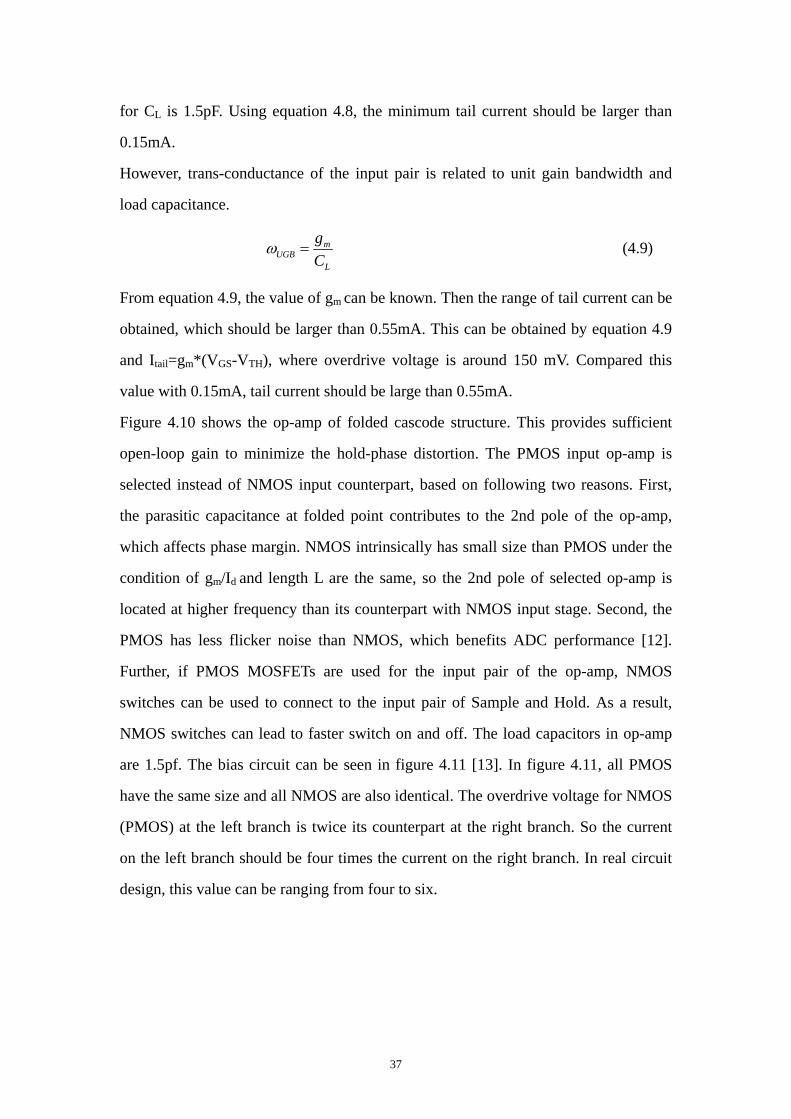
Figure 4.10 shows the op-amp of folded cascode structure. This provides sufficient
open-loop gain to minimize the hold-phase distortion. The PMOS input op-amp is
selected instead of NMOS input counterpart, based on following two reasons. First,
the parasitic capacitance at folded point contributes to the 2nd pole of the op-amp,
which affects phase margin. NMOS intrinsically has small size than PMOS under the
condition of gm/Id and length L are the same, so the 2nd pole of selected op-amp is
located at higher frequency than its counterpart with NMOS input stage. Second, the
PMOS has less flicker noise than NMOS, which benefits ADC performance [12].
Further, if PMOS MOSFETs are used for the input pair of the op-amp, NMOS
switches can be used to connect to the input pair of Sample and Hold. As a result,
NMOS switches can lead to faster switch on and off. The load capacitors in op-amp
are 1.5pf. The bias circuit can be seen in figure 4.11 [13]. In figure 4.11, all PMOS
have the same size and all NMOS are also identical. The overdrive voltage for NMOS
(PMOS) at the left branch is twice its counterpart at the right branch. So the current
on the left branch should be four times the current on the right branch. In real circuit
design, this value can be ranging from four to six.
38
Figure 4.10 folded cascode op-amp
vdd
Vbn
Vcn
Vcp
Vbp
I1 I2
Figure 4.11 bias circuit for op-amp
39
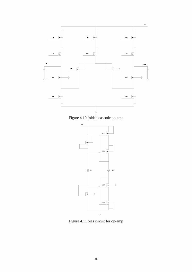
4.4.2 Common mode feedback
In reality, there are a lot of factors will influence the output voltage of op-amp. Such
as temperature, mismatch. The purpose to add common mode feedback is to keep the
common mode voltage at the output stable. Generally speaking, common mode is
assumed to be half of the supply voltage. In my op-amp design, switch-capacitor
common mode feedback circuit is used instead of continuous one in order to save the
power consumption.
Figure 4.12 shows the structure of common mode feedback circuit. In the reset mode,
clock signal Sn1 goes high and S1 goes low. All the switches turn on at this moment.
Common mode output voltage equals to reference voltage which is 600mV. The
capacitors sustain a voltage Vref-Vbs. In the amplification mode, clock signal Sn1
goes low and S1 goes high. All the switches turn off at this time. However, the bias
currents in figure 4.10 don’t change, so voltage Vbs remains the same value. As a
result, the output common-mode voltage equals to Vbs+(Vref-Vbs)=Vref=600mV,
which ensures the common-mode voltage constant in the amplification mode.
40
Figure 4.12 switched capacitor common mode feedback
4.4.3 Simulation result
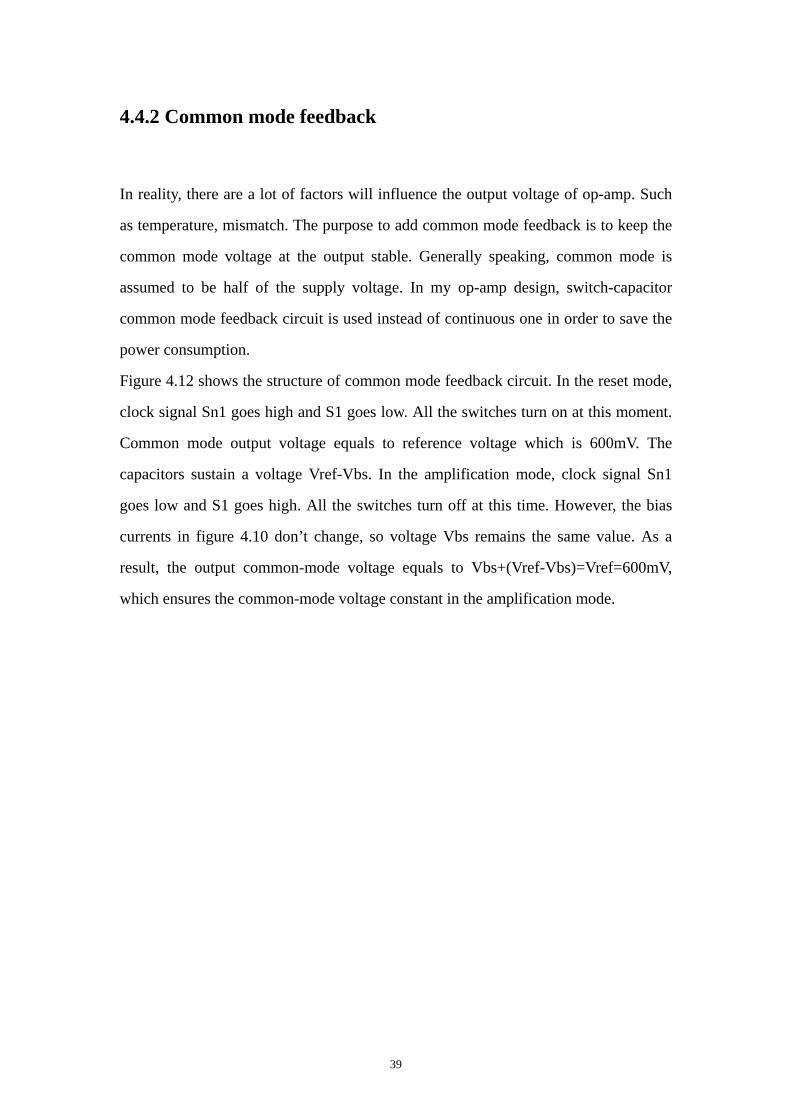
The AC simulation result of my op-amp can be seen in figure 4.13. We can see gain of
op-amp is 43.8dB, unit gain frequency is around 702.6MHz and phase margin is
around 70 degree. In table 4.1, more parameters of op-amp will be shown. From this
table, the result of bandwidth meets the analysis requirement above.
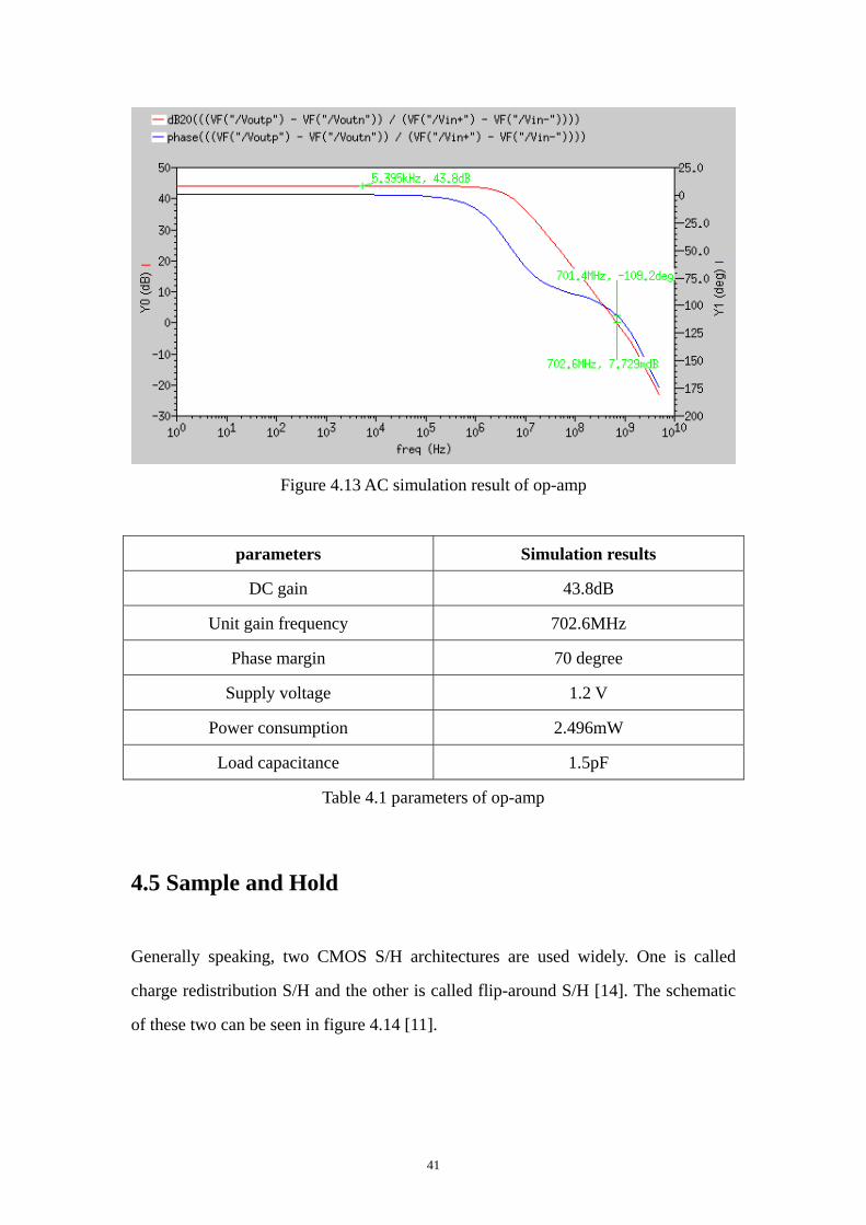
41
Figure 4.13 AC simulation result of op-amp
parameters Simulation results
DC gain 43.8dB
Unit gain frequency 702.6MHz
Phase margin 70 degree
Supply voltage 1.2 V
Power consumption 2.496mW
Load capacitance 1.5pF
Table 4.1 parameters of op-amp
4.5 Sample and Hold
Generally speaking, two CMOS S/H architectures are used widely. One is called
charge redistribution S/H and the other is called flip-around S/H [14]. The schematic
of these two can be seen in figure 4.14 [11].
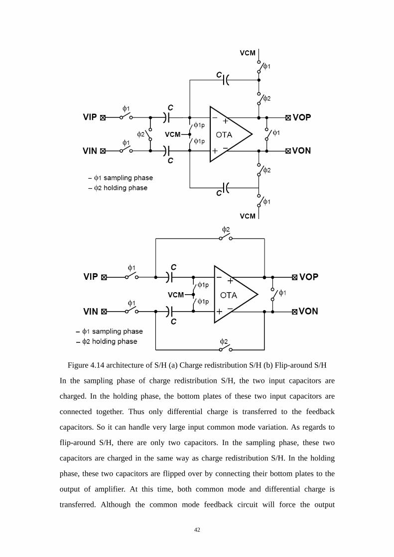
42
Figure 4.14 architecture of S/H (a) Charge redistribution S/H (b) Flip-around S/H
In the sampling phase of charge redistribution S/H, the two input capacitors are
charged. In the holding phase, the bottom plates of these two input capacitors are
connected together. Thus only differential charge is transferred to the feedback
capacitors. So it can handle very large input common mode variation. As regards to
flip-around S/H, there are only two capacitors. In the sampling phase, these two
capacitors are charged in the same way as charge redistribution S/H. In the holding
phase, these two capacitors are flipped over by connecting their bottom plates to the
output of amplifier. At this time, both common mode and differential charge is
transferred. Although the common mode feedback circuit will force the output
43
common mode to a nominal value, the common mode for the input of amplifier will
change if the signal’s input common mode level is different from the output one. As a
result, amplifier must handle large input common mode variation. However,
flip-around S/H is more popular in high speed ADC design because its low power
consumption, low noise and smaller size [12].
gnd
vdd
gnd
vdd
gnd
vdd
gnd
vdd
gnd
gnd
gnd
OPAMP
gnd
voutp
voutn
vinp
vinn
Sn1
S1
Sn2
S2
Sn1
S1
Sn2
S2
Sn1
Sn1
S3
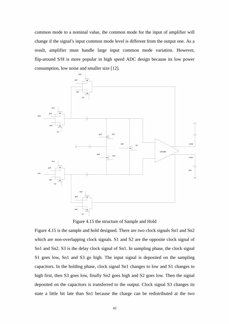
Figure 4.15 the structure of Sample and Hold
Figure 4.15 is the sample and hold designed. There are two clock signals Sn1 and Sn2
which are non-overlapping clock signals. S1 and S2 are the opposite clock signal of
Sn1 and Sn2. S3 is the delay clock signal of Sn1. In sampling phase, the clock signal
S1 goes low, Sn1 and S3 go high. The input signal is deposited on the sampling
capacitors. In the holding phase, clock signal Sn1 changes to low and S1 changes to
high first, then S3 goes low, finally Sn2 goes high and S2 goes low. Then the signal
deposited on the capacitors is transferred to the output. Clock signal S3 changes its
state a little bit late than Sn1 because the charge can be redistributed at the two
44
differential input of the op-amp, which gives rise to cancel charge injection influence
at the top plates of two capacitors.
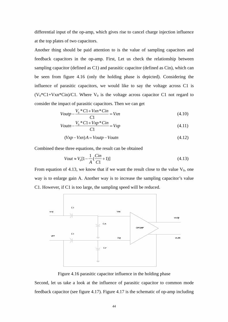
Another thing should be paid attention to is the value of sampling capacitors and
feedback capacitors in the op-amp. First, Let us check the relationship between
sampling capacitor (defined as C1) and parasitic capacitor (defined as Cin), which can
be seen from figure 4.16 (only the holding phase is depicted). Considering the
influence of parasitic capacitors, we would like to say the voltage across C1 is
(V0*C1+Vxn*Cin)/C1. Where V0 is the voltage across capacitor C1 not regard to
consider the impact of parasitic capacitors. Then we can get
0 * 1 *1
V C Vxn CinVoutp VxnC+
− = (4.10)
0 * 1 *1
V C Vxp CinVoutn VxpC+
− = (4.11)
( )Vxp Vxn A Voutp Voutn− = − (4.12)
Combined these three equations, the result can be obtained
01[1 ( 1)]
1CinVout V
A C≈ − + (4.13)
From equation of 4.13, we know that if we want the result close to the value V0, one
way is to enlarge gain A. Another way is to increase the sampling capacitor’s value
C1. However, if C1 is too large, the sampling speed will be reduced.
Figure 4.16 parasitic capacitor influence in the holding phase
Second, let us take a look at the influence of parasitic capacitor to common mode
feedback capacitor (see figure 4.17). Figure 4.17 is the schematic of op-amp including
45
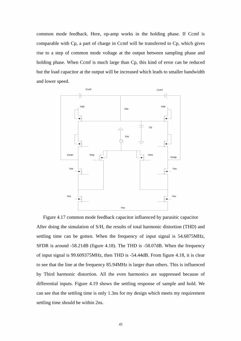
common mode feedback. Here, op-amp works in the holding phase. If Ccmf is
comparable with Cp, a part of charge in Ccmf will be transferred to Cp, which gives
rise to a step of common mode voltage at the output between sampling phase and
holding phase. When Ccmf is much large than Cp, this kind of error can be reduced
but the load capacitor at the output will be increased which leads to smaller bandwidth
and lower speed.
Vss
Vss
Vss
Vss
Vss
Vss
Vbs
Ccmf Ccmf
Cp
Vdd Vdd
Vinp VinnVoutp
Voutn
Figure 4.17 common mode feedback capacitor influenced by parasitic capacitor
After doing the simulation of S/H, the results of total harmonic distortion (THD) and
settling time can be gotten. When the frequency of input signal is 54.6875MHz,
SFDR is around -58.21dB (figure 4.18). The THD is -58.07dB. When the frequency
of input signal is 99.609375MHz, then THD is -54.44dB. From figure 4.18, it is clear
to see that the line at the frequency 85.94MHz is larger than others. This is influenced
by Third harmonic distortion. All the even harmonics are suppressed because of
differential inputs. Figure 4.19 shows the settling response of sample and hold. We
can see that the settling time is only 1.3ns for my design which meets my requirement
settling time should be within 2ns.
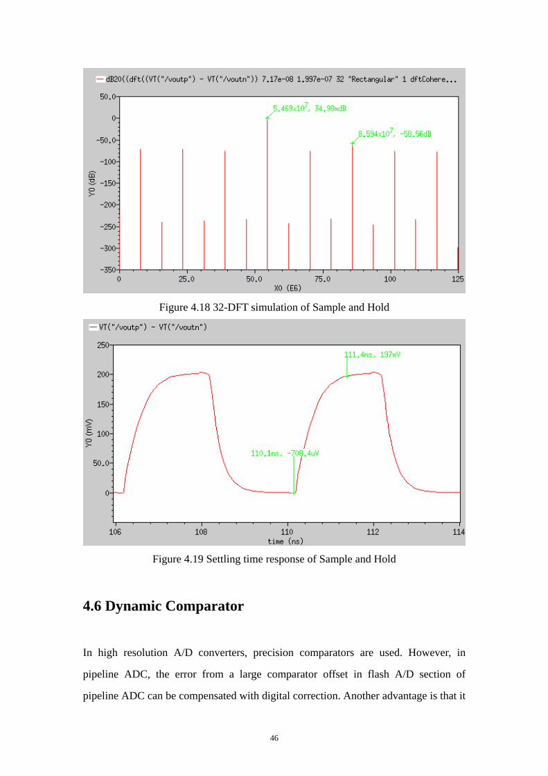
46
Figure 4.18 32-DFT simulation of Sample and Hold
Figure 4.19 Settling time response of Sample and Hold
4.6 Dynamic Comparator
In high resolution A/D converters, precision comparators are used. However, in
pipeline ADC, the error from a large comparator offset in flash A/D section of
pipeline ADC can be compensated with digital correction. Another advantage is that it
47
saves power by using simple dynamic comparator in low resolution flash A/D
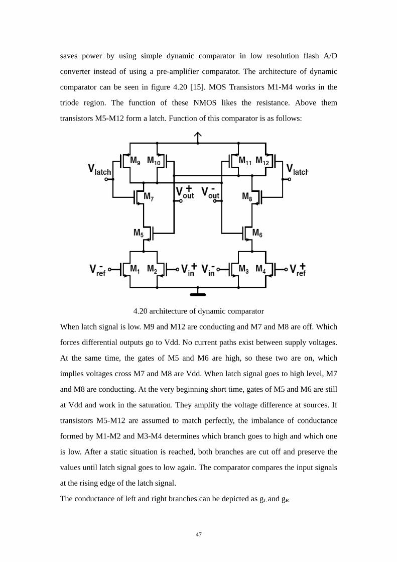
converter instead of using a pre-amplifier comparator. The architecture of dynamic
comparator can be seen in figure 4.20 [15]. MOS Transistors M1-M4 works in the
triode region. The function of these NMOS likes the resistance. Above them
transistors M5-M12 form a latch. Function of this comparator is as follows:
4.20 architecture of dynamic comparator
When latch signal is low. M9 and M12 are conducting and M7 and M8 are off. Which
forces differential outputs go to Vdd. No current paths exist between supply voltages.
At the same time, the gates of M5 and M6 are high, so these two are on, which
implies voltages cross M7 and M8 are Vdd. When latch signal goes to high level, M7
and M8 are conducting. At the very beginning short time, gates of M5 and M6 are still
at Vdd and work in the saturation. They amplify the voltage difference at sources. If
transistors M5-M12 are assumed to match perfectly, the imbalance of conductance
formed by M1-M2 and M3-M4 determines which branch goes to high and which one
is low. After a static situation is reached, both branches are cut off and preserve the
values until latch signal goes to low again. The comparator compares the input signals
at the rising edge of the latch signal.
The conductance of left and right branches can be depicted as gL and gR.
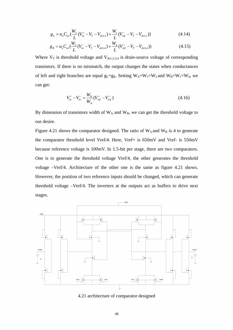
48
2 11,2 1,2( ( ) ( ))L n ox in T ds ref T ds
W Wg u C V V V V V VL L
+ −= − − + − − (4.14)
3 43,4 3,4( ( ) ( ))R n ox in T ds ref T ds
W Wg u C V V V V V VL L
− += − − + − − (4.15)
Where VT is threshold voltage and Vds1,2,3,4 is drain-source voltage of corresponding
transistors. If there is no mismatch, the output changes the states when conductances
of left and right branches are equal gL=gR. Setting WA=W2=W3 and WB=W1=W4, we
can get:
( )Bin in ref ref
A
WV V V VW
+ − + −− = − (4.16)
By dimension of transistors width of WA and WB, we can get the threshold voltage to
our desire.
Figure 4.21 shows the comparator designed. The ratio of WA and WB is 4 to generate
the comparator threshold level Vref/4. Here, Vref+ is 650mV and Vref- is 550mV
because reference voltage is 100mV. In 1.5-bit per stage, there are two comparators.
One is to generate the threshold voltage Vref/4, the other generates the threshold
voltage –Vref/4. Architecture of the other one is the same as figure 4.21 shows.
However, the position of two reference inputs should be changed, which can generate
threshold voltage –Vref/4. The inverters at the outputs act as buffers to drive next
stages.
Vdd
C
voutp
C
voutn
Vref+Vin-Vin+Vref-
latch
4.21 architecture of comparator designed
49
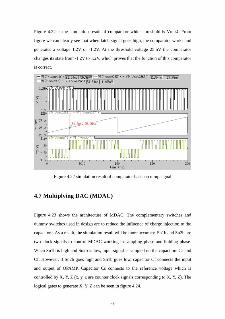
Figure 4.22 is the simulation result of comparator which threshold is Vref/4. From
figure we can clearly see that when latch signal goes high, the comparator works and
generates a voltage 1.2V or -1.2V. At the threshold voltage 25mV the comparator
changes its state from -1.2V to 1.2V, which proves that the function of this comparator
is correct.
Figure 4.22 simulation result of comparator basis on ramp signal
4.7 Multiplying DAC (MDAC)
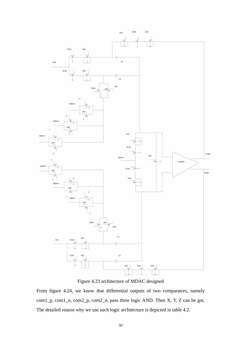
Figure 4.23 shows the architecture of MDAC. The complementary switches and
dummy switches used in design are to reduce the influence of charge injection to the
capacitors. As a result, the simulation result will be more accuracy. Sn1b and Sn2b are
two clock signals to control MDAC working in sampling phase and holding phase.
When Sn1b is high and Sn2b is low, input signal is sampled on the capacitors Cs and
Cf. However, if Sn2b goes high and Sn1b goes low, capacitor Cf connects the input
and output of OPAMP. Capacitor Cs connects to the reference voltage which is
controlled by X, Y, Z (x, y, z are counter clock signals corresponding to X, Y, Z). The
logical gates to generate X, Y, Z can be seen in figure 4.24.
50
vdd
vdd
vdd
vdd
vdd
vdd
vdd
vdd
650mV
600mV
550mV
550mV
600mV
650mV
vinp
Sn1b
Sn1b
S1b
S1b
Sn2bS2b S2b
Sn2bS2b
S1b
Sn1b
Sn1b
150mV
S1b
S3b
OPAMP
Voutp
Voutn
X
x
Z
z
Y
y
Y
y Z
z
X
x
Sn2b
S2b
Sn1bS1b
Sn1b S1b
Sn2bS2b S2b
vinn
Cf
Cs
Cf
Cs
Figure 4.23 architecture of MDAC designed
From figure 4.24, we know that differential outputs of two comparators, namely
com1_p, com1_n, com2_p, com2_n, pass three logic AND. Then X, Y, Z can be got.
The detailed reason why we use such logic architecture is depicted in table 4.2.
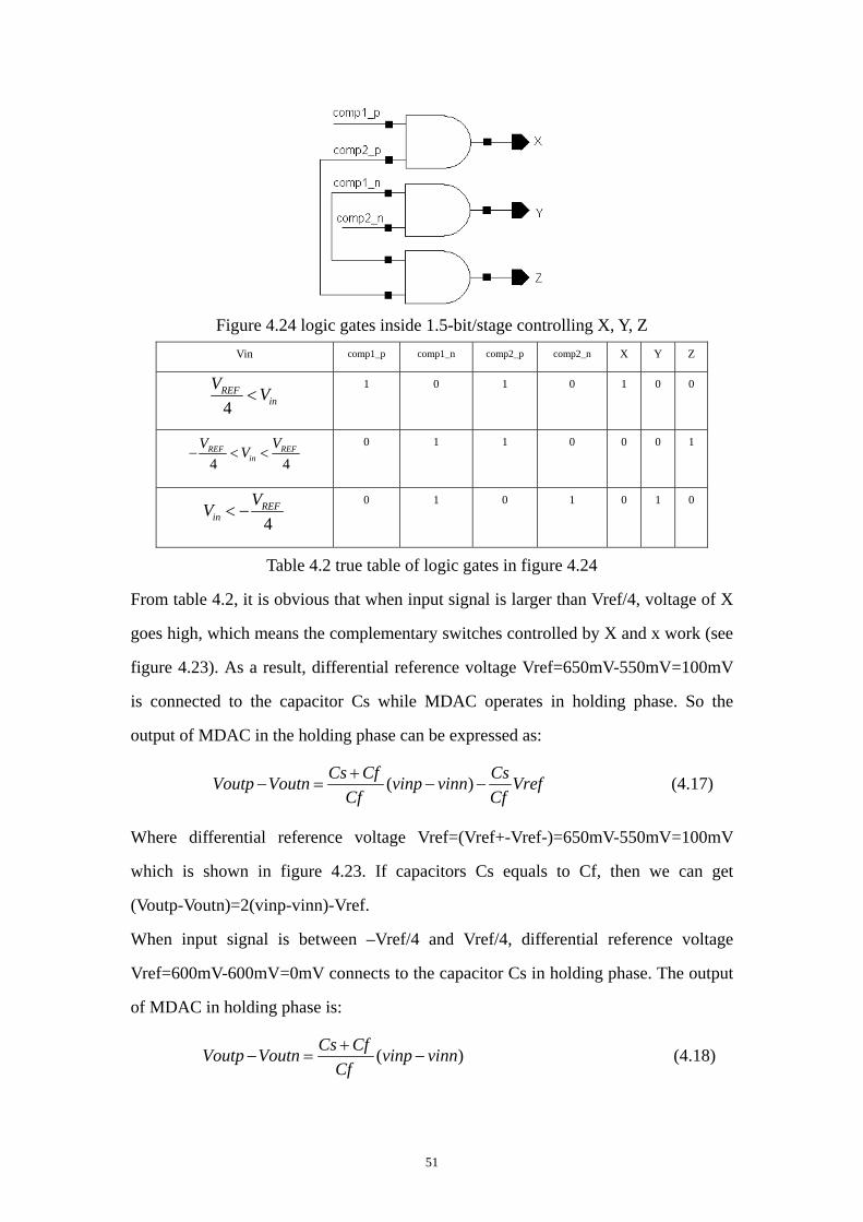
51
Figure 4.24 logic gates inside 1.5-bit/stage controlling X, Y, Z Vin comp1_p comp1_n comp2_p comp2_n X Y Z
4REF
inV V<
1 0 1 0 1 0 0
4 4REF REF
inV VV− < <
0 1 1 0 0 0 1
4REF
inVV < −
0 1 0 1 0 1 0
Table 4.2 true table of logic gates in figure 4.24
From table 4.2, it is obvious that when input signal is larger than Vref/4, voltage of X
goes high, which means the complementary switches controlled by X and x work (see
figure 4.23). As a result, differential reference voltage Vref=650mV-550mV=100mV
is connected to the capacitor Cs while MDAC operates in holding phase. So the
output of MDAC in the holding phase can be expressed as:
( )Cs Cf CsVoutp Voutn vinp vinn VrefCf Cf+
− = − − (4.17)
Where differential reference voltage Vref=(Vref+-Vref-)=650mV-550mV=100mV
which is shown in figure 4.23. If capacitors Cs equals to Cf, then we can get
(Voutp-Voutn)=2(vinp-vinn)-Vref.
When input signal is between –Vref/4 and Vref/4, differential reference voltage
Vref=600mV-600mV=0mV connects to the capacitor Cs in holding phase. The output
of MDAC in holding phase is:
( )Cs CfVoutp Voutn vinp vinnCf+
− = − (4.18)
52
If Cs equals to Cf, then equation (Voutp-Voutn)=2(vinp-vinn) is obtained.
When input signal is smaller than –Vref/4, differential reference voltage
–Vref=550mV-650mV=-100mV is connected to the capacitor Cs of MDAC in holding
phase. Then the output of MDAC can be written:
( )Cs Cf CsVoutp Voutn vinp vinn VrefCf Cf+
− = − + (4.19)
If Cf has the same value with Cs, then 4.19 can be changed to
(Voup-Voutn)=2(vinp-vinn)+Vref.
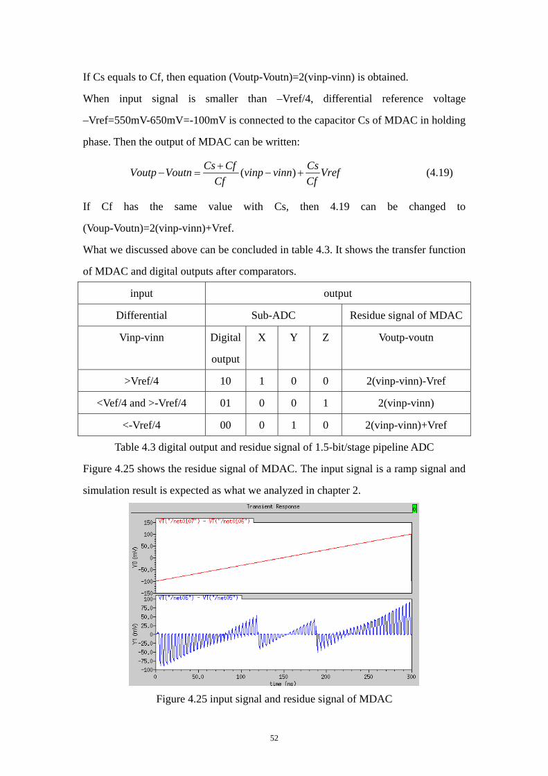
What we discussed above can be concluded in table 4.3. It shows the transfer function
of MDAC and digital outputs after comparators.
input output
Differential Sub-ADC Residue signal of MDAC
Vinp-vinn Digital
output
X Y Z Voutp-voutn
>Vref/4 10 1 0 0 2(vinp-vinn)-Vref
<Vef/4 and >-Vref/4 01 0 0 1 2(vinp-vinn)
<-Vref/4 00 0 1 0 2(vinp-vinn)+Vref
Table 4.3 digital output and residue signal of 1.5-bit/stage pipeline ADC
Figure 4.25 shows the residue signal of MDAC. The input signal is a ramp signal and
simulation result is expected as what we analyzed in chapter 2.
Figure 4.25 input signal and residue signal of MDAC
53
4.8 D flip-flop In pipeline ADC, there are several similar N-bit per stage architecture. Each of them is
controlled by two phases-sampling and holding. In this case, however, the digital
output of each stage is not generated at the same time. Time difference (delay) is
existed for these digital outputs. In order to get all the digital outputs at the same time,
we need to use registers to keep data until the digital output from last stage generated.
Then all the outputs can be processed by digital correction at the same time.
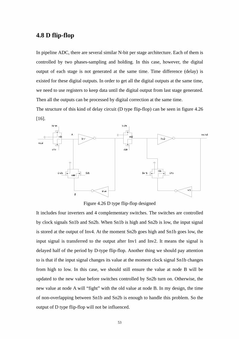
The structure of this kind of delay circuit (D type flip-flop) can be seen in figure 4.26
[16].
Figure 4.26 D type flip-flop designed
It includes four inverters and 4 complementary switches. The switches are controlled
by clock signals Sn1b and Sn2b. When Sn1b is high and Sn2b is low, the input signal
is stored at the output of Inv4. At the moment Sn2b goes high and Sn1b goes low, the
input signal is transferred to the output after Inv1 and Inv2. It means the signal is
delayed half of the period by D-type flip-flop. Another thing we should pay attention
to is that if the input signal changes its value at the moment clock signal Sn1b changes
from high to low. In this case, we should still ensure the value at node B will be
updated to the new value before switches controlled by Sn2b turn on. Otherwise, the
new value at node A will “fight” with the old value at node B. In my design, the time
of non-overlapping between Sn1b and Sn2b is enough to handle this problem. So the
output of D type flip-flop will not be influenced.
54
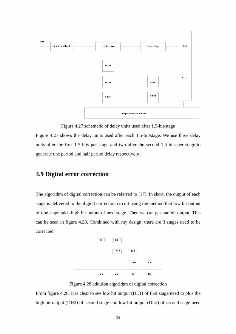
Figure 4.27 schematic of delay units used after 1.5-bit/stage
Figure 4.27 shows the delay units used after each 1.5-bit/stage. We use three delay
units after the first 1.5 bits per stage and two after the second 1.5 bits per stage to
generate one period and half period delay respectively.
4.9 Digital error correction
The algorithm of digital correction can be referred to [17]. In short, the output of each
stage is delivered to the digital correction circuit using the method that low bit output
of one stage adds high bit output of next stage. Then we can get one bit output. This
can be seen in figure 4.28. Combined with my design, there are 3 stages need to be
corrected.
Figure 4.28 addition algorithm of digital correction
From figure 4.28, it is clear to see low bit output (DL1) of first stage need to plus the
high bit output (DH2) of second stage and low bit output (DL2) of second stage need
55
to add the high bit output (DH3) of flash ADC except DH1 and DL3. The adder I used
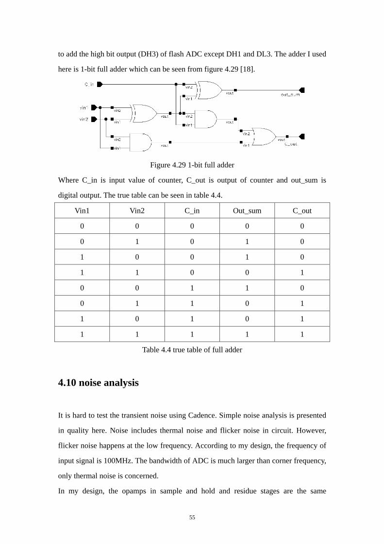
here is 1-bit full adder which can be seen from figure 4.29 [18].
Figure 4.29 1-bit full adder
Where C_in is input value of counter, C_out is output of counter and out_sum is
digital output. The true table can be seen in table 4.4.
Vin1 Vin2 C_in Out_sum C_out
0 0 0 0 0
0 1 0 1 0
1 0 0 1 0
1 1 0 0 1
0 0 1 1 0
0 1 1 0 1
1 0 1 0 1
1 1 1 1 1
Table 4.4 true table of full adder
4.10 noise analysis
It is hard to test the transient noise using Cadence. Simple noise analysis is presented
in quality here. Noise includes thermal noise and flicker noise in circuit. However,
flicker noise happens at the low frequency. According to my design, the frequency of
input signal is 100MHz. The bandwidth of ADC is much larger than corner frequency,
only thermal noise is concerned.
In my design, the opamps in sample and hold and residue stages are the same
56
structure. If noise in the residue stage is known, so does the noise in sample and hold.
Noise of residue stage contains two parts. One is the on resistance of switches and the
other is opamp noise [19].
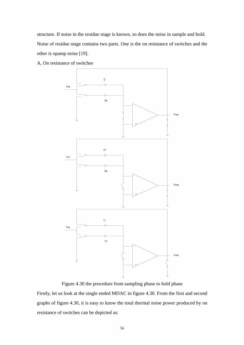
A, On resistance of switches
Figure 4.30 the procedure from sampling phase to hold phase
Firstly, let us look at the single ended MDAC in figure 4.30. From the first and second
graphs of figure 4.30, it is easy to know the total thermal noise power produced by on
resistance of switches can be depicted as:
57
2
tot s f opamp
KT KTVC C C C
= =+ +
(4.20)
2 2( * ) ( )n s f opampQ C V KT C C C= = + + (4.21)
When MDAC transfers the condition from sampling phase to holding phase (see third
graph in figure 4.30), the thermal noise power at the output can be expressed as:
2
22 2
( ) 1s f opampnout
f f f
C C CQ KTV KTC C C f
+ += = = (4.22)
Where f=Cf/(Cs+Cf+Copamp) is the feedback factor, Copamp is the input capacitor of the
op-amp. Then the input-referred noise power can be written as:
2
2 22 2
( )1 ( )( )
f s f opampoutin
f f s s f
C KT C C CV KTVG C f C C C C
+ += = =
+ + (4.23)
Where G is the gain of MDAC.
B, Opamp noise
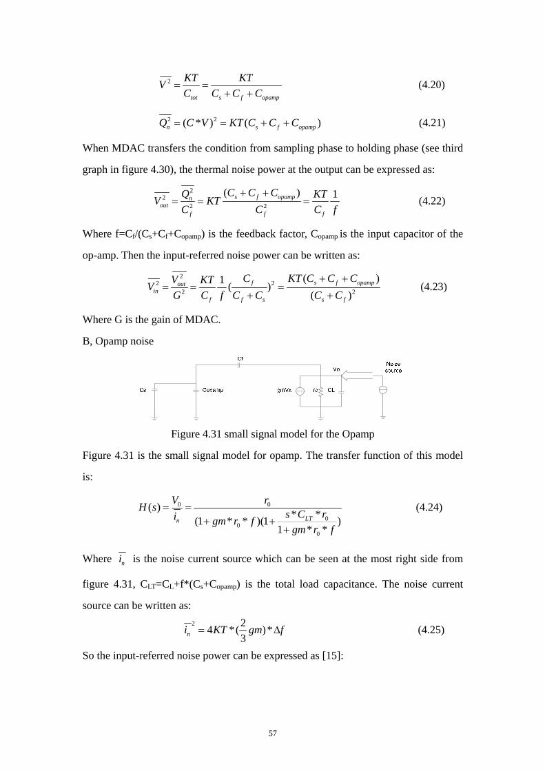
Figure 4.31 small signal model for the Opamp
Figure 4.31 is the small signal model for opamp. The transfer function of this model
is:
0 0
00
0
( ) * *(1 * * )(1 )1 * *
LTn
V rH s s C ri gm r fgm r f
= =+ +
+
(4.24)
Where ni is the noise current source which can be seen at the most right side from
figure 4.31, CLT=CL+f*(Cs+Copamp) is the total load capacitance. The noise current
source can be written as:
2 24 *( )*
3ni KT gm f= Δ (4.25)
So the input-referred noise power can be expressed as [15]:
58
222
2 20 02 2
(| ( | ) | * ) 2 1 1 ( )3
j n fin
LT s f
H s i CVV KTG G f C C C
ω
∞
∫= = =
+ (4.26)
Considering the differential circuit, the total input-referred noise power of first residue
stage is:
2 2,1 2
2 ( ) 4 1 1 ( )( ) 3
s f opamp ftotal
s f LT s f
KT C C C CV KT
C C f C C C+ +
= ++ +
(4.27)
The Op-amps in SHA and MDAC are the same. The only difference is that there is
only one capacitor for sampling and holding in SHA, however, there are two
capacitors Cs and Cf in MDAC. So it is easy to get the input-referred noise of SHA if
Cs and f in equation 4.26 are set to be 0 and 1. The input-referred noise of SHA can
be written as:
22
2 ( ) 4 13
F opampopamp
F LT
KT C CV KT
C C+
= + (4.28)
Where CF is sampling capacitor in SHA and CL is load capacitor.
The total input referred noise at the input of ADC can be found by summing all the
noise components from subsequent stages and is given by:
2 2 2 2,1 ,2
1 ...4total opamp total totalV V V V= + + + (4.29)
Because the gain of residue stage is 2, the noise power transferred from the output of
second residue stage to the input of ADC is only 4 times smaller. As regards to the
third residue stage, the noise power which transfers to the input of ADC is only 16
times smaller. This value can be neglected. That is reason why only the noise from
SHA and next two residue stages is considered in equation 4.29.
From what we talked above, it is obviously to see that the sampling capacitor CF of
SHA and Cs, Cf of MDAC, input capacitor Copamp, load capacitor CL of SHA and CL of
MDAC influence input-referred noise power of ADC vey much. Increasing the value
CF, Cs, Cf, CL, CL and reducing the value Copamp are two ways to reduce the noise power
of ADC. However, increasing CF, Cs, Cf mean it needs more time to settling for ADC.
Increasing CL and CL mean the bandwidth of ADC becomes smaller. Reducing Copamp
means the gain of opamp is smaller. It needs to consider all these tradeoff when
59
designing the circuit.
As a whole, this chapter presents the detail of each block of pipeline ADC and shows
the simulation result of them. At last, noise of the whole system is analyzed to depict
which part contributes noise significantly. Next Chapter, simulation results of the
whole pipeline ADC will be given including graphs and data.

60
61
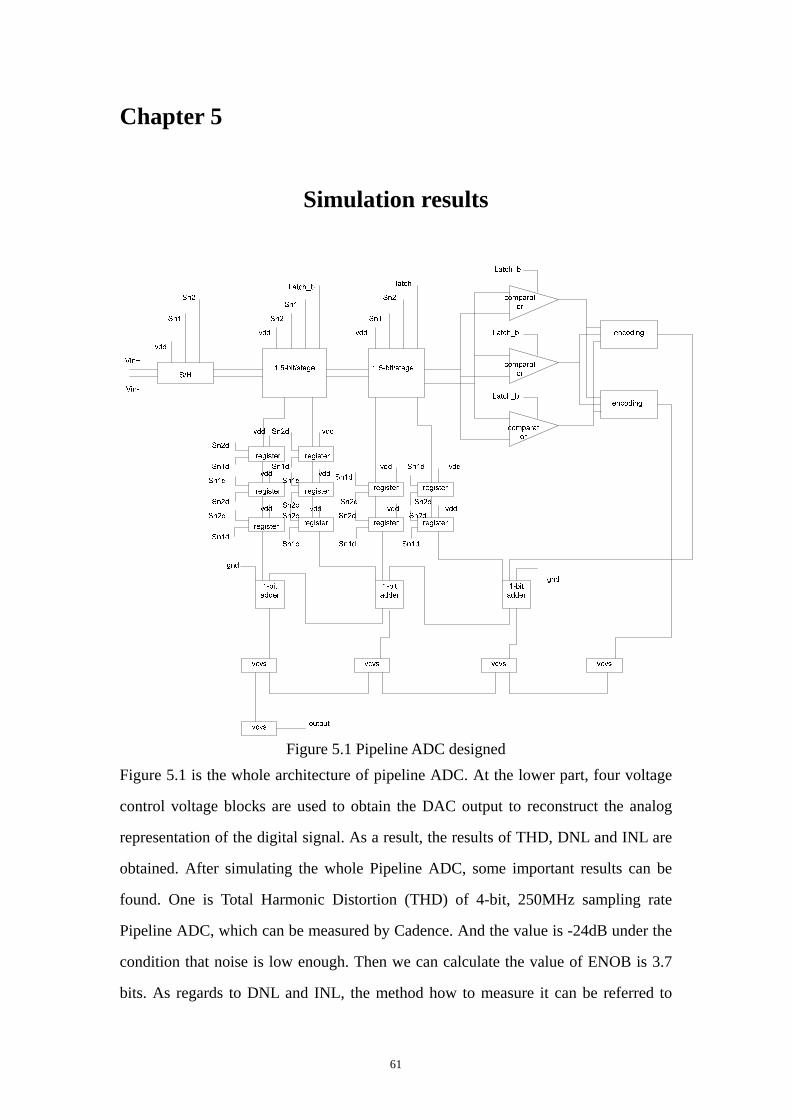
Chapter 5
Simulation results
Figure 5.1 Pipeline ADC designed Figure 5.1 is the whole architecture of pipeline ADC. At the lower part, four voltage
control voltage blocks are used to obtain the DAC output to reconstruct the analog
representation of the digital signal. As a result, the results of THD, DNL and INL are
obtained. After simulating the whole Pipeline ADC, some important results can be
found. One is Total Harmonic Distortion (THD) of 4-bit, 250MHz sampling rate
Pipeline ADC, which can be measured by Cadence. And the value is -24dB under the
condition that noise is low enough. Then we can calculate the value of ENOB is 3.7
bits. As regards to DNL and INL, the method how to measure it can be referred to
62
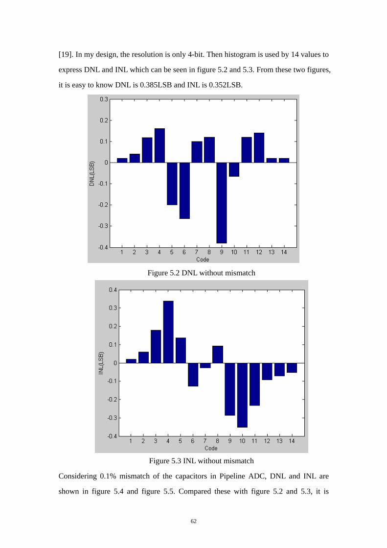
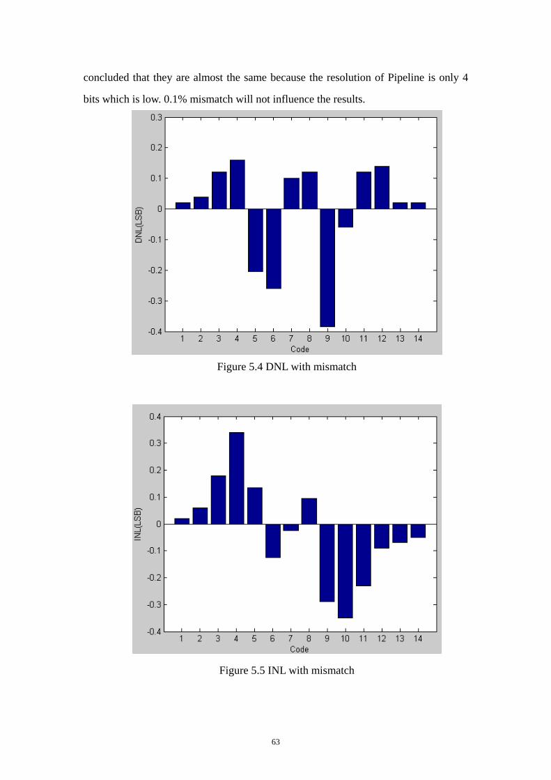
[19]. In my design, the resolution is only 4-bit. Then histogram is used by 14 values to
express DNL and INL which can be seen in figure 5.2 and 5.3. From these two figures,
it is easy to know DNL is 0.385LSB and INL is 0.352LSB.
Figure 5.2 DNL without mismatch
Figure 5.3 INL without mismatch
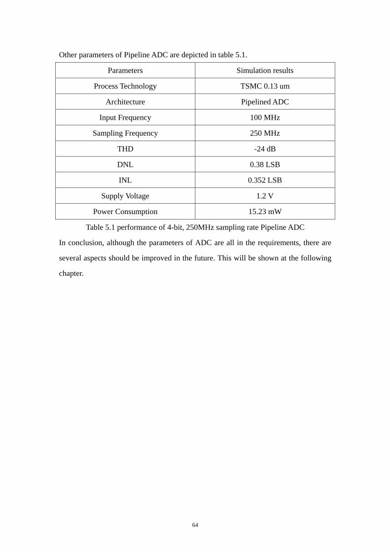
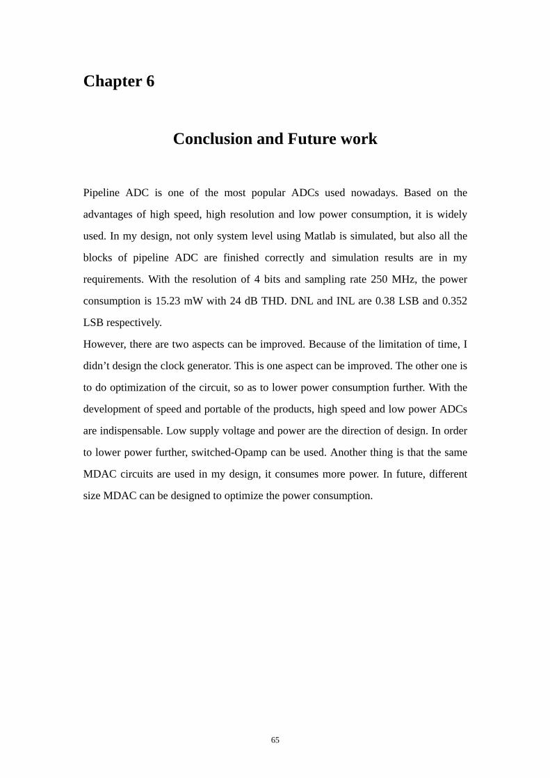
Considering 0.1% mismatch of the capacitors in Pipeline ADC, DNL and INL are
shown in figure 5.4 and figure 5.5. Compared these with figure 5.2 and 5.3, it is
63
concluded that they are almost the same because the resolution of Pipeline is only 4
bits which is low. 0.1% mismatch will not influence the results.
Figure 5.4 DNL with mismatch
Figure 5.5 INL with mismatch
64
Other parameters of Pipeline ADC are depicted in table 5.1.
Parameters Simulation results
Process Technology TSMC 0.13 um
Architecture Pipelined ADC
Input Frequency 100 MHz
Sampling Frequency 250 MHz
THD -24 dB
DNL 0.38 LSB
INL 0.352 LSB
Supply Voltage 1.2 V
Power Consumption 15.23 mW
Table 5.1 performance of 4-bit, 250MHz sampling rate Pipeline ADC
In conclusion, although the parameters of ADC are all in the requirements, there are
several aspects should be improved in the future. This will be shown at the following
chapter.
65
Chapter 6
Conclusion and Future work
Pipeline ADC is one of the most popular ADCs used nowadays. Based on the
advantages of high speed, high resolution and low power consumption, it is widely
used. In my design, not only system level using Matlab is simulated, but also all the
blocks of pipeline ADC are finished correctly and simulation results are in my
requirements. With the resolution of 4 bits and sampling rate 250 MHz, the power
consumption is 15.23 mW with 24 dB THD. DNL and INL are 0.38 LSB and 0.352
LSB respectively.
However, there are two aspects can be improved. Because of the limitation of time, I
didn’t design the clock generator. This is one aspect can be improved. The other one is
to do optimization of the circuit, so as to lower power consumption further. With the
development of speed and portable of the products, high speed and low power ADCs
are indispensable. Low supply voltage and power are the direction of design. In order
to lower power further, switched-Opamp can be used. Another thing is that the same
MDAC circuits are used in my design, it consumes more power. In future, different
size MDAC can be designed to optimize the power consumption.

66
67
References
[1] P.E. Allen, D. R. Holberg, “CMOS Analog Circuit Design”, Oxford University
Press, Second edition, 2002.
[2] Brian P. Ginsburg, Anantha P. Chandrakasan, “Dual Time-Interleaved Successive
Approximation Register ADCs for an Ultra-Wideband Receiver”, IEEE Journal of
Solid-State Circuits, Vol. 42, NO. 2, pp. 247-257, February 2007.
[3] A.Abo, “Design for Reliability of Low-Voltage, Switch-Capacitor Circuits”,
Doctoral Thesis, University of California, Berkeley, May 1999.
[4] W. C. Song, H. W. Choi, S. U. Kwak, and B. S. Song, “A 10-b 20-Msample/s
Low-Power CMOS ADC”, IEEE J. Solid-State Circuits, Vol. 30, No. 5, pp. 514-521,
May 1995.
[5] B. Razavi, “Principles of Data Conversion System Design”, McGraw-Hill
Publishers, 1995.
[6] D. A. Johns and K. Martin, “Analog Integrated Circuit Design”, John Wiley and
Sons Publishers, 1997.
[7] Tsung-Hsien Lu, Chun-Kuei Chiu, Ching-Cheng Tien, “A 10 Bits 40-MS/s
Pipelined Analog-to-Digital Converter for IEEE 802.11a WLAN Systems”,
Department of Electrical Engineering, Chung-Hua University, Taiwan, 2007.
[8] B. Boser, EECS 247 lecture 18: Pipelined ADC, UC Berkeley, 2002.
[9] Michael S. Chang and Kaiann L. Fu, Students, “An 86 mW, 80 Msample/sec,
10-bit Pipeline ADC”, Project Paper, EECS 598 Mixed-Signal Circuit Design, 2002.
[10] Behzad Razavi, “Design of Analog CMOS Integrated Circuit,” McGraw-Hill
International Edition, 2001.
[11] Jipeng Li, “Accuracy Enhancement Techniques in Low-Voltage High-Speed
Pipelined ADC Design”, Doctoral Thesis, Oregon State University, October 2003.
[12] Wenhua (Will) Yang, Dan Kelly, Iuri Mehr, Mark T. Sayuk, and Larry Singer, “A
3-V 340-mW 14-b 75-Msample/s CMOS ADC With 85-dB SFDR at Nyquist Input”,
IEEE Journal of Solid-State Circuit, Vol. 36, NO. 12, pp. 1931-1936, December 2001.
68
[13] Klaas Bult, “ET4295 Introduction to Analog CMOS Design,” E-mail:
[14] Ronak Trivedi, “Low power and high speed sample-and-hold circuit”, in
proceedings of 49th IEEE International Midwest Symposium on Circuits and Systems,
Vol. 1, pp. 453-456, 6-9 August 2006.
[15] T. Cho, “Low-Power Low-Voltage Analog-to-Digital Conversion Techniques
using Pipelined Architectures,” Doctoral Thesis, UC Berkeley, 1995.
[16] Jian Zhou, Jin Liu and Dian Zhou, “Reduced setup time static D flip-flop”,
Electronics Letters, Vol. 37, pp. 279-280, 1 March 2001.
[17] J. Haze, R. Vrba, “A Novel 10-bit, 40MHz, 54mW Pipelined ADC”, Dept. of
Microelectronics, FEEC, BUT Brno, Czech Republic, 15 November 2005.
[18] Akshay Visweswaran, Kamran Suori, and David A. Calvillo, “A 1.2V, 8-bit,
1-MSps Pipeline Analog-to-Digital Converter on CMOS 130nm technology”, Delft
University of Technology ET4168 “Design of Nyquist-Rate Data Converters” Course
Project.
[19] Wouter A. Serdijn, Raza Lotfi, Lecture notes “Nyquist-rate data converters”,
Delft University of Technology, Faculty of Electrical Engineering, Mathematics and
Computer Science, Electronics Research Laboratory, Mekelweg 4, 2628 CD Delft,
The Netherlands. [email protected], [email protected].


![Fianl Adidas Original[2]](https://img.pdfslide.us/doc/110x75/547291fdb4af9f980a8b4f1d/fianl-adidas-original2.jpg)