Embed Size (px)
DESCRIPTION
Redes, teoremas, conversiones
Citation preview
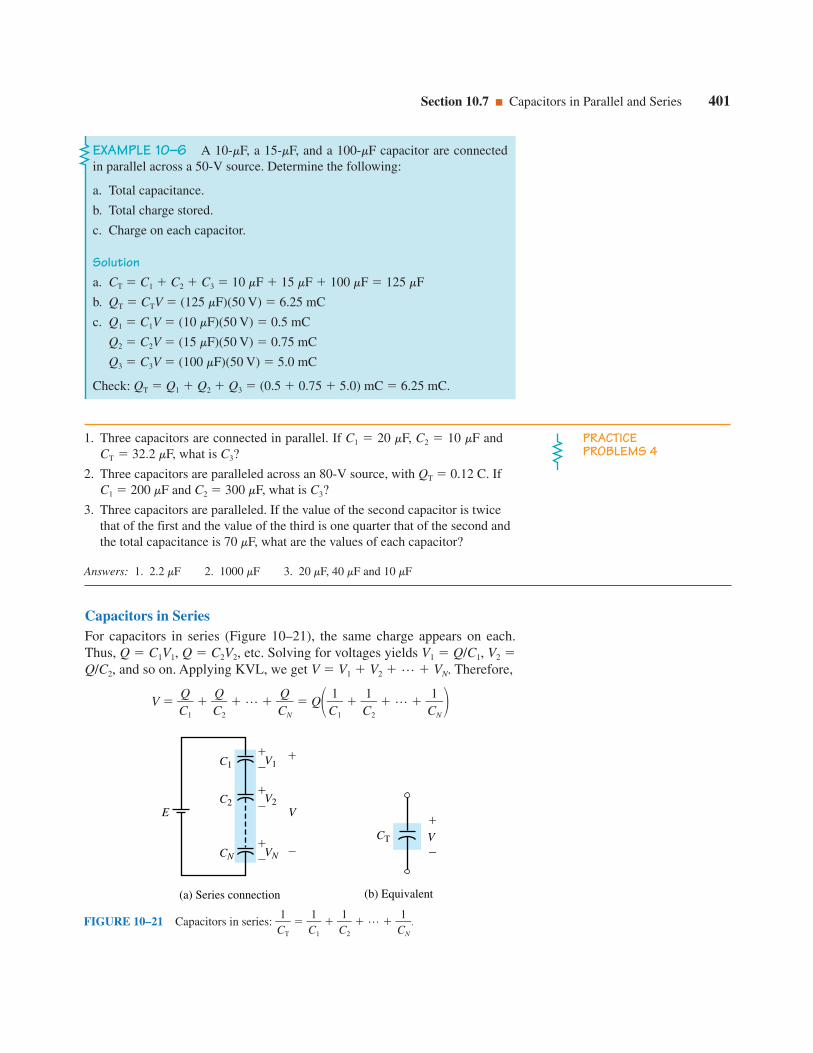
Capacitors in SeriesFor capacitors in series (Figure 10–21), the same charge appears on each.Thus, Q C1V1, Q C2V2, etc. Solving for voltages yields V1 Q/C1, V2 Q/C2, and so on. Applying KVL, we get V V1 V2 … VN. Therefore,
V CQ
1
CQ
2
… CQ
N
QC1
1
C1
2
… C1
N
Section 10.7 Capacitors in Parallel and Series 401
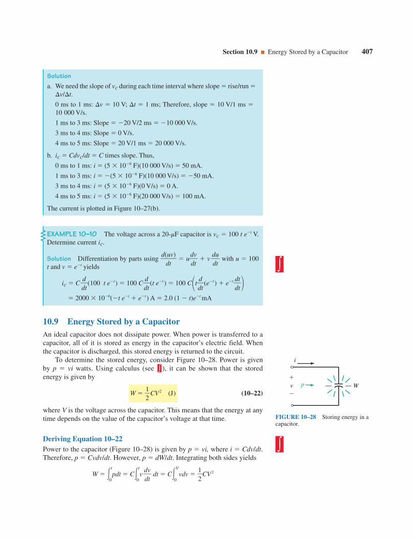
EXAMPLE 10–6 A 10-mF, a 15-mF, and a 100-mF capacitor are connectedin parallel across a 50-V source. Determine the following:
a. Total capacitance.
b. Total charge stored.
c. Charge on each capacitor.
Solutiona. CT C1 C2 C3 10 mF 15 mF 100 mF 125 mF
b. QT CTV (125 mF)(50 V) 6.25 mC
c. Q1 C1V (10 mF)(50 V) 0.5 mC
Q2 C2V (15 mF)(50 V) 0.75 mC
Q3 C3V (100 mF)(50 V) 5.0 mC
Check: QT Q1 Q2 Q3 (0.5 0.75 5.0) mC 6.25 mC.
PRACTICEPROBLEMS 4
1. Three capacitors are connected in parallel. If C1 20 mF, C2 10 mF andCT 32.2 mF, what is C3?
2. Three capacitors are paralleled across an 80-V source, with QT 0.12 C. IfC1 200 mF and C2 300 mF, what is C3?
3. Three capacitors are paralleled. If the value of the second capacitor is twicethat of the first and the value of the third is one quarter that of the second andthe total capacitance is 70 mF, what are the values of each capacitor?
Answers: 1. 2.2 mF 2. 1000 mF 3. 20 mF, 40 mF and 10 mF
FIGURE 10–21 Capacitors in series: C1
T
C1
1
C1
2
… C1
N
.
(a) Series connection
V1
EV2
VN
V
C1
C2
CN
V
(b) Equivalent
CT

402 Chapter 10 Capacitors and Capacitance
EXAMPLE 10–7 Refer to Figure 10–22(a):
a. Determine CT.
b. If 50 V is applied across the capacitors, determine Q.
c. Determine the voltage on each capacitor.
Solution
a. C1
T
C1
1
C1
2
C1
3
30
1mF
601mF
201mF
0.0333 106 0.0167 106 0.05 106 0.1 106
Therefore as indicated in (b),
CT 0.1
1106 10 mF
b. Q CTV (10 106 F)(50 V) 0.5 mC
c. V1 Q/C1 (0.5 103 C)/(30 106 F) 16.7 V
V2 Q/C2 (0.5 103 C)/(60 106 F) 8.3 V
V3 Q/C3 (0.5 103 C)/(20 106 F) 25.0 V
Check: V1 V2 V3 16.7 8.3 25 50 V.
CTC3C2C1
30 µF 10 µF60 µF 20 µF
(a) (b)
FIGURE 10–22
1. For capacitors in parallel,total capacitance is alwayslarger than the largest capaci-tance, while for capacitors inseries, total capacitance isalways smaller than thesmallest capacitance.
2. The formula for capacitors inparallel is similar to the for-mula for resistors in series,while the formula for capaci-tors in series is similar to theformula for resistors in par-allel.
NOTES...
But V Q/CT. Equating this with the right side and cancelling Q yields
C1
T
C1
1
C1
2
… C1
N
(10–15)
For two capacitors in series, this reduces to
CT C
C
1 1C
C2
2
(10–16)
For N equal capacitors in series, Equation 10–15 yields CT C/N.

Voltage Divider Rule for Series CapacitorsFor capacitors in series (Figure 10–24) a simple voltage divider rule can bedeveloped. Recall, for individual capacitors, Q1 C1V1, Q2 C2V2, etc., andfor the complete string, QT CTVT. As noted earlier, Q1 Q2 … QT.Thus, C1V1 CTVT. Solving for V1 yields
V1 C
CT
1
VT
Section 10.7 Capacitors in Parallel and Series 403
EXAMPLE 10–8 For the circuit of Figure 10–23(a), determine CT.
Solution The problem is easily solved through step-by-step reduction. C2
and C3 in parallel yield 45 mF 15 mF 60 mF. C4 and C5 in parallel total20 mF. The reduced circuit is shown in (b). The two 60-mF capacitances inseries reduce to 30 mF. The series combination of 30 mF and 20 mF can befound from Equation 10–16. Thus,
CT 3300
m
m
FF
2200
m
m
FF
12 mF
Alternately, you can reduce (b) directly using Equation 10–15. Try it.
12 F
60 F
20 F
30 F
CT
(c)
60 F
CT 20 F
12 FCT
60 F
45 F
CT 8 FC5C4
15 F
C2
C3
C1
(b)
(a)
FIGURE 10–23 Systematic reduction.
V1
V2
V3
E
VT
FIGURE 10–24 Capacitive voltagedivider.

This type of relationship holds for all capacitors. Thus,
Vx C
CT
x
VT (10–17)
From this, you can see that the voltage across a capacitor is inversely propor-tional to its capacitance, that is, the smaller the capacitance, the larger thevoltage, and vice versa. Other useful variations are
V1 C
C2
1
V2, V1 C
C3
1
V3, V2 C
C3
2
V3, etc.
404 Chapter 10 Capacitors and Capacitance
PRACTICEPROBLEMS 5
1. Verify the voltages of Example 10–7 using the voltage divider rule for capaci-tors.
2. Determine the voltage across each capacitor of Figure 10–23 if the voltageacross C5 is 30 V.
Answers: 1. V1 16.7 V V2 8.3 V V3 25.0 V 2. V1 10 V V2 V3 10 VV4 V5 30 V
10.8 Capacitor Current and VoltageAs noted earlier (Figure 10–2), during charging, electrons are moved fromone plate of a capacitor to the other plate. Several points should be noted.
1. This movement of electrons constitutes a current.
2. This current lasts only long enough for the capacitor to charge. When thecapacitor is fully charged, current is zero.
3. Current in the circuit during charging is due solely to the movement ofelectrons from one plate to the other around the external circuit; no cur-rent passes through the dielectric between the plates.
4. As charge is deposited on the plates, the capacitor voltage builds. How-ever, this voltage does not jump to full value immediately since it takestime to move electrons from one plate to the other. (Billions of electronsmust be moved.)
5. Since voltage builds up as charging progresses, the difference in voltagebetween the source and the capacitor decreases and hence the rate ofmovement of electrons (i.e., the current) decreases as the capacitorapproaches full charge.
Figure 10–25 shows what the voltage and current look like during thecharging process. As indicated, the current starts out with an initial surge,then decays to zero while the capacitor voltage gradually climbs from zeroto full voltage. The charging time typically ranges from nanoseconds to mil-liseconds, depending on the resistance and capacitance of the circuit. (Westudy these relationships in detail in Chapter 11.) A similar surge (but in theopposite direction) occurs during discharge.
As Figure 10–25 indicates, current exists only while the capacitor volt-age is changing. This observation turns out to be true in general, that is,

current in a capacitor exists only while capacitor voltage is changing. Thereason is not hard to understand. As you saw before, a capacitor’s dielectricis an insulator and consequently no current can pass through it (assumingzero leakage). The only charges that can move, therefore, are the free elec-trons that exist on the capacitor’s plates. When capacitor voltage is con-stant, these charges are in equilibrium, no net movement of charge occurs,and the current is thus zero. However, if the source voltage is increased,additional electrons are pulled from the positive plate; inversely, if thesource voltage is decreased, excess electrons on the negative plate arereturned to the positive plate. Thus, in both cases, capacitor current resultswhen capacitor voltage is changed. As we show next, this current is propor-tional to the rate of change of voltage. Before we do this, however, weneed to look at symbols.
Symbols for Time-Varying Voltages and CurrentsQuantities that vary with time are called instantaneous quantities. Standardindustry practice requires that we use lowercase letters for time-varyingquantities, rather than capital letters as for dc. Thus, we use vC and iC to rep-resent changing capacitor voltage and current rather than VC and IC. (Oftenwe drop the subscripts and just use v and i.) Since these quantities are func-tions of time, they may also be shown as vC(t) and iC(t).
Capacitor v-i RelationshipThe relationship between charge and voltage for a capacitor is given byEquation 10–1. For the time-varying case, it is
q CvC (10–18)
But current is the rate of movement of charge. In calculus notation, this isiC dq/dt. Differentiating Equation 10–18 yields
iC d
d
q
t
d
d
t(CvC) (10–19)
Section 10.8 Capacitor Current and Voltage 405
FIGURE 10–25 The capacitor does not charge instantaneously, as a finite amount oftime is required to move electrons around the circuit.
R
vCE
iC
(a) (b) Current surge during charging. Currentis zero when fully charged.
Beforecharging
Duringcharging
Aftercharging
Current decaysas capacitor
charges
Time
iC
(c) Capacitor voltage. vC = Ewhen fully charged.
Voltage buildsas capacitor charges
Time
E
vC
Calculus is introduced at thispoint to aid in the developmentof ideas and to help explainconcepts. However, not every-one who uses this book requirescalculus. Therefore, the materialis presented in such a mannerthat it never relies entirely onmathematics; thus, where calcu-lus is used, intuitive explana-tions accompany it. However, toprovide the enrichment that cal-culus offers, optional derivationsand problems are included, butthey are marked with a iconso that they may be omitted ifdesired.
∫
NOTES...

Since C is constant, we get
iC Cd
d
v
tC
(A) (10–20)
Equation 10–20 shows that current through a capacitor is equal to C timesthe rate of change of voltage across it. This means that the faster the voltagechanges, the larger the current, and vice versa. It also means that if the volt-age is constant, the current is zero (as we noted earlier).
Reference conventions for voltage and current are shown in Figure 10–26. As usual, the plus sign goes at the tail of the current arrow. If the voltageis increasing, dvC /dt is positive and the current is in the direction of the refer-ence arrow; if the voltage is decreasing, dvC /dt is negative and the current isopposite to the arrow.
The derivative dvC /dt of Equation 10–20 is the slope of the capacitorvoltage versus time curve. When capacitor voltage varies linearly with time(i.e., the relationship is a straight line as in Figure 10–27), Equation 10–20reduces to
iC CD
D
v
tC
Cr
r
i
u
s
n
e C slope of the line (10–21)
406 Chapter 10 Capacitors and Capacitance
vC
iC
FIGURE 10–26 The sign for vC
goes at the tail of the current arrow.
EXAMPLE 10–9 A signal generator applies voltage to a 5-mF capacitorwith a waveform as in Figure 10–27(a). The voltage rises linearly from 0 to10 V in 1 ms, falls linearly to 10 V at t 3 ms, remains constant until t 4 ms,rises to 10 V at t 5 ms, and remains constant thereafter.
a. Determine the slope of vC in each time interval.
b. Determine the current and sketch its graph.
10
–101 2 3 4 5
vC (V)
t(mS)0
Slope = 20 000 V/s
Slope = −10 000 V/s
Slope = 10 000 V/s
(a)
(b)
50
1 2 3 4 5 6–50
iC (mA)
t (mS)
100 mA
FIGURE 10–27
10.9 Energy Stored by a CapacitorAn ideal capacitor does not dissipate power. When power is transferred to acapacitor, all of it is stored as energy in the capacitor’s electric field. Whenthe capacitor is discharged, this stored energy is returned to the circuit.
To determine the stored energy, consider Figure 10–28. Power is givenby p vi watts. Using calculus (see ), it can be shown that the storedenergy is given by
W 12
CV2 (J) (10–22)
where V is the voltage across the capacitor. This means that the energy at anytime depends on the value of the capacitor’s voltage at that time.
Deriving Equation 10–22Power to the capacitor (Figure 10–28) is given by p vi, where i Cdv/dt.Therefore, p Cvdv/dt. However, p dW/dt. Integrating both sides yields
W t
0pdt Ct
0v
ddvt dt CV
0vdv
12
CV2
∫
Section 10.9 Energy Stored by a Capacitor 407
Solutiona. We need the slope of vC during each time interval where slope rise/run
Dv/Dt.
0 ms to 1 ms: Dv 10 V; Dt 1 ms; Therefore, slope 10 V/1 ms 10 000 V/s.
1 ms to 3 ms: Slope 20 V/2 ms 10 000 V/s.
3 ms to 4 ms: Slope 0 V/s.
4 ms to 5 ms: Slope 20 V/1 ms 20 000 V/s.
b. iC CdvC/dt C times slope. Thus,
0 ms to 1 ms: i (5 106 F)(10 000 V/s) 50 mA.
1 ms to 3 ms: i (5 106 F)(10 000 V/s) 50 mA.
3 ms to 4 ms: i (5 106 F)(0 V/s) 0 A.
4 ms to 5 ms: i (5 106 F)(20 000 V/s) 100 mA.
The current is plotted in Figure 10–27(b).
EXAMPLE 10–10 The voltage across a 20-mF capacitor is vC 100 t et V.Determine current iC.
Solution Differentiation by parts using d(
dutv) u
ddvt v
ddut with u 100
t and v et yields
iC C ddt(100 t et) 100 C
ddt(t et) 100 Ct
ddt(et) et
ddtt
2000 106(t et et) A 2.0 (1 t)et mA
∫
v p
i
W
FIGURE 10–28 Storing energy in acapacitor.
∫

10.10 Capacitor Failures and TroubleshootingAlthough capacitors are quite reliable, they may fail because of misapplica-tion, excessive voltage, current, temperature, or simply because they age.They can short internally, leads may become open, dielectrics may becomeexcessively leaky, and they may fail catastrophically due to incorrect use. (Ifan electrolytic capacitor is connected with its polarity reversed, for example,it may explode.) Capacitors should be used well within their rating limits.Excessive voltage can lead to dielectric puncture creating pinholes that shortthe plates together. High temperatures may cause an increase in leakageand/or a permanent shift in capacitance. High temperatures may be causedby inadequate heat removal, excessive current, lossy dielectrics, or an oper-ating frequency beyond the capacitor’s rated limit.
Basic Testing with an OhmmeterSome basic (out-of-circuit) tests can be made with an analog ohmmeter. Theohmmeter can detect opens and shorts and, to a certain extent, leakydielectrics. First, ensure that the capacitor is discharged, then set the ohmme-ter to its highest range and connect it to the capacitor. (For electrolyticdevices, ensure that the plus () side of the ohmmeter is connected to theplus () side of the capacitor.)
408 Chapter 10 Capacitors and Capacitance
Capacitor
(a) Measuring C with a DMM. (Not all DMMs can measure capacitance)
(b) Capacitor/inductor analyzer. (Courtesy B + K Precision)
FIGURE 10–29 Capacitor testing.
Initially, the ohmmeter reading should be low, then for a good capacitorgradually increase to infinity as the capacitor charges through the ohmmetercircuit. (Or at least a very high value, since most good capacitors, exceptelectrolytics, have a resistance of hundreds of megohms.) For small capaci-tors, however, the time to charge may be too short to yield useful results.
Faulty capacitors respond differently. If a capacitor is shorted, the meterresistance reading will stay low. If it is leaky, the reading will be lower thannormal. If it is open circuited, the meter will indicate infinity immediately,without dipping to zero when first connected.
Capacitor TestersOhmmeter testing of capacitors has its limitations; other tools may be needed.Figure 10–29 shows two of them. The DMM in (a) can measure capacitanceand display it directly on its readout. The LCR (inductance, capacitance, resis-tance) analyzer in (b) can determine capacitance as well as detect opens andshorts. More sophisticated testers are available that determine capacitancevalue, leakage at rated voltage, dielectric absorption, and so on.
Problems 409
PROBLEMS10.1 Capacitance
1. For Figure 10–30, determine the charge on the capacitor, its capacitance, orthe voltage across it as applicable for each of the following.
a. E 40 V, C 20 mF b. V 500 V, Q 1000 mC
c. V 200 V, C 500 nF d. Q 3 104 C, C 10 106 F
e. Q 6 mC, C 40 mF f. V 1200 V, Q 1.8 mC
2. Repeat Question 1 for the following:
a. V 2.5 kV, Q 375 mC b. V 1.5 kV, C 0.04 104 F
c. V 150 V, Q 6 105 C d. Q 10 mC, C 400 nF
e. V 150 V, C 40 105 F f. Q 6 109 C, C 800 pF
3. The charge on a 50-mF capacitor is 10 103 C. What is the potential dif-ference between its terminals?
4. When 10 mC of charge is placed on a capacitor, its voltage is 25 V. What isthe capacitance?
5. You charge a 5-mF capacitor to 150 V. Your lab partner then momentarilyplaces a resistor across its terminals and bleeds off enough charge that itsvoltage falls to 84 V. What is the final charge on the capacitor?
10.2 Factors Affecting Capacitance
6. A capacitor with circular plates 0.1 m in diameter and an air dielectric has0.1 mm spacing between its plates. What is its capacitance?
7. A parallel-plate capacitor with a mica dielectric has dimensions of 1 cm 1.5 cm and separation of 0.1 mm. What is its capacitance?
8. For the capacitor of Problem 7, if the mica is removed, what is its newcapacitance?
E C V+
−
FIGURE 10–30

9. The capacitance of an oil-filled capacitor is 200 pF. If the separationbetween its plates is 0.1 mm, what is the area of its plates?
10. A 0.01-mF capacitor has ceramic with a dielectric constant of 7500. If theceramic is removed, the plate separation doubled, and the spacing betweenplates filled with oil, what is the new value for C?
11. A capacitor with a Teflon dielectric has a capacitance of 33 mF. A secondcapacitor with identical physical dimensions but with a Mylar dielectric car-ries a charge of 55 104 C. What is its voltage?
12. The plate area of a capacitor is 4.5 in2. and the plate separation is 5 mils. Ifthe relative permittivity of the dielectric is 80, what is C?
10.3 Electric Fields
13. a. What is the electric field strength at a distance of 1 cm from a 100-mCcharge in transformer oil?
b. What is at twice the distance?
14. Suppose that 150 V is applied across a 100-pF parallel-plate capacitorwhose plates are separated by 1 mm. What is the electric field intensity between the plates?
10.4 Dielectrics
15. An air-dielectric capacitor has plate spacing of 1.5 mm. How much voltagecan be applied before breakdown occurs?
16. Repeat Problem 15 if the dielectric is mica and the spacing is 2 mils.
17. A mica-dielectric capacitor breaks down when E volts is applied. The micais removed and the spacing between plates doubled. If breakdown nowoccurs at 500 V, what is E?
18. Determine at what voltage the dielectric of a 200 nF Mylar capacitor with aplate area of 0.625 m2 will break down.
19. Figure 10–31 shows several gaps, including a parallel-plate capacitor, a setof small spherical points, and a pair of sharp points. The spacing is the samefor each. As the voltage is increased, which gap breaks down for each case?
20. If you continue to increase the source voltage of Figures 10–31(a), (b), and(c) after a gap breaks down, will the second gap also break down? Justifyyour answer.
10.5 Nonideal Effects
21. A 25-mF capacitor has a negative temperature coefficient of 175 ppm/°C. Byhow much and in what direction might it vary if the temperature rises by50°C? What would be its new value?
22. If a 4.7-mF capacitor changes to 4.8 mF when the temperature rises 40°C,what is its temperature coefficient?
10.7 Capacitors in Parallel and Series
23. What is the equivalent capacitance of 10 mF, 12 mF, 22 mF, and 33 mF con-nected in parallel?
24. What is the equivalent capacitance of 0.10 mF, 220 nF, and 4.7 107 Fconnected in parallel?
25. Repeat Problem 23 if the capacitors are connected in series.
410 Chapter 10 Capacitors and Capacitance
Plates Points
(a)
(b)
(c)
SpheresPoints
PlatesSpheres
FIGURE 10–31 Source voltage isincreased until one of the gaps breaksdown. (The source has high internalresistance to limit current followingbreakdown.)

26. Repeat Problem 24 if the capacitors are connected in series.
27. Determine CT for each circuit of Figure 10–32.
28. Determine total capacitance looking in at the terminals for each circuit ofFigure 10–33.
Problems 411
C2
a
b
CT
C1
C3
12 µF
120 µF
80 µF
(a)
C2
a
b
CT
C1 C3
4 µF
1 µF
8 µF
(b)
4 F
5 F
CT
C1
C2
C3
6 Fa
b
(c)
C1
C2 C3
C4
C6C5
(d)
3 F
2 FCT
6 F
a
b
1 F 1 F
500 nF
FIGURE 10–32
a
b
CT
0.47 µF 0.22 µF
47 µF0.15 µF
(a)
a
b
CT
0.0005 µF
100 pF
500 pF
100 pF
1000 pF
(b)
a b 47 µF
0.1 µF1 µF
CT
10 µF
100 000 pF
4.7µF
(c)
2.2µF
16a
b
1416
18 12
10
10
5 4
3.2
CT
(d) All values in F
FIGURE 10–33

29. A 30-mF capacitor is connected in parallel with a 60-mF capacitor, and a10-mF capacitor is connected in series with the parallel combination. Whatis CT?
30. For Figure 10–34, determine Cx.
412 Chapter 10 Capacitors and Capacitance
40 F
10 F
Cx20 F
40 F
30 F
C420 F
C3 = 2C4
FIGURE 10–34
31. For Figure 10–35, determine C3 and C4.
32. For Figure 10–36, determine CT.
FIGURE 10–35
75 FV = 10 V
50 F
CTQ = 100 C
FIGURE 10–36
20 F V3
60 F
30 F120 V
V1
V2
FIGURE 10–37
33. You have capacitors of 22 mF, 47 mF, 2.2 mF and 10 mF. Connecting theseany way you want, what is the largest equivalent capacitance you can get?The smallest?
34. A 10-mF and a 4.7-mF capacitor are connnected in parallel. After a thirdcapacitor is added to the circuit, CT 2.695 mF. What is the value of thethird capacitor? How is it connected?
35. Consider capacitors of 1 mF, 1.5 mF, and 10 mF. If CT 10.6 mF, how are thecapacitors connected?
36. For the capacitors of Problem 35, if CT 2.304 mF, how are the capacitorsconnected?
37. For Figures 10–32(c) and (d), find the voltage on each capacitor if 100 V isapplied to terminals a-b.
38. Use the voltage divider rule to find the voltage across each capacitor of Fig-ure 10–37.
39. Repeat Problem 38 for the circuit of Figure 10–38.
40. For Figure 10–39, Vx 50 V. Determine Cx and CT.
41. For Figure 10–40, determine Cx.
42. A dc source is connected to terminals a-b of Figure 10–34. If Cx is 12 mFand the voltage across the 40-mF capacitor is 80 V,
a. What is the source voltage?
b. What is the total charge on the capacitors?

c. What is the charge on each individual capacitor?
10.8 Capacitor Current and Voltage
43. The voltage across the capacitor of Figure 10–41(a) is shown in (b). Sketchcurrent iC scaled with numerical values.
Problems 413
25 F
40 F
16 F60 V
V1
V2
35 F V3
FIGURE 10–38
CxVx
50 F
75 F100 V
FIGURE 10–39
40 F
500 F
Cx100 V
1200 F
100 F
16 V
FIGURE 10–40
(a)
(b)
30
20
10
0
101 2 3 4 5 6 7 8 9
vC
t (ms)
5 F
iC
vC
FIGURE 10–41

44. The current through a 1-mF capacitor is shown in Figure 10–42. Sketch volt-age vC scaled with numerical values. Voltage at t 0 s is 0 V.
45. If the voltage across a 4.7-mF capacitor is vC 100e0.05t V, what is iC?
10.9 Energy Stored by a Capacitor
46. For the circuit of Figure 10–37, determine the energy stored in each capacitor.
47. For Figure 10–41, determine the capacitor’s energy at each of the followingtimes: t 0, 1 ms, 4 ms, 5 ms, 7 ms, and 9 ms.
10.10 Capacitor Failures and Troubleshooting
48. For each case shown in Figure 10–43, what is the likely fault?
414 Chapter 10 Capacitors and Capacitance
8.92 nF
DATA HOLD
POWER MAJAVG D/0 MHZ/120HZ
RANGE
UNIVERSAL LCR METER
L/C/R TOL RECALL
(a)
0.068 µF C3
0.015 µF
0.022 µF
C1
C2
0.132 µF
DATA HOLD
POWER MAJAVG D/0 MHZ/120HZ
RANGE
UNIVERSAL LCR METER
L/C/R TOL RECALL
(b)
0.033 µF
0.33 µF
C1
C2C3
0.22 µF
(c)
0.47 F 0.1 F
C3
C2C1
100 V 0.22 F
68.1 V
40
20
0 1 2 3 4 5
i (mA)
t (mS)-20
FIGURE 10–42
FIGURE 10–43 For each case, what is the likely fault?
∫
In-Process Learning Check 1
1. a. 2.12 nF
b. 200 V
2. It becomes 6 times larger.
3. 1.1 nF
4. mica
Answers to In-Process Learning Checks 415
ANSWERS TO IN-PROCESSLEARNING CHECKS
OBJECTIVES
After studying this chapter, you will beable to
• explain why transients occur in RC cir-cuits,
• explain why an uncharged capacitorlooks like a short circuit when first ener-gized,
• describe why a capacitor looks like anopen circuit to steady state dc,
• describe charging and discharging ofsimple RC circuits with dc excitation,
• determine voltages and currents in sim-ple RC circuits during charging and dis-charging,
• plot voltage and current transients,
• understand the part that time constantsplay in determining the duration of tran-sients,
• compute time constants,
• describe the use of charging and dis-charging waveforms in simple timingapplications,
• calculate the pulse response of simpleRC circuits,
• solve simple RC transient problemsusing Electronics Workbench andPSpice.
KEY TERMS
Capacitive Loading
Exponential Functions
Initial Conditions
Pulse
Pulse Width (tp)
Rise and Fall Times (tr, tf)
Step Voltages
Time Constant (t RC)
Transient
Transient Duration (5t)
OUTLINE
Introduction
Capacitor Charging Equations
Capacitor with an Initial Voltage
Capacitor Discharging Equations
More Complex Circuits
An RC Timing Application
Pulse Response of RC Circuits
Transient Analysis Using Computers
Capacitor Charging,Discharging, and SimpleWaveshaping Circuits
11

As you saw in Chapter 10, capacitors do not charge or discharge instanta-neously. Instead, as illustrated in Figure 10–25, voltages and currents take
time to reach their new values. The time taken to reach these new values (i.e., thecharge and discharge times) are dependent on the resistance and capacitance ofthe circuit. During charge, for example, a capacitor charges at a rate determinedby its capacitance and the resistance through which it charges, while during dis-charge, it discharges at a rate determined by its capacitance and the resistancethrough which it discharges. Since the voltages and currents that exist duringthese charging and discharging times are transitory in nature, they are calledtransients. Transients do not last very long, typically only a fraction of a sec-ond. However, they are important to us for a number of reasons, some of whichyou will learn in this chapter.
Transients occur in both capacitive and inductive circuits. In capacitive cir-cuits, they occur because capacitor voltage cannot change instantaneously; ininductive circuits, they occur because inductor current cannot change instanta-neously. In this chapter, we look at capacitive transients; in Chapter 14, we lookat inductive transients. As you will see, many of the basic principles are thesame.
Note: Optional problems and derivations using calculus are marked bya icon. They may be omitted without loss of continuity by those who do notrequire calculus.
∫
417
CHAPTER PREVIEW
Desirable and Undesirable Transients
TRANSIENTS OCCUR IN CAPACITIVE and inductive circuits whenever circuit con-ditions are changed, for example, by the sudden application of a voltage, theswitching in or out of a circuit element, or the malfunctioning of a circuit com-ponent. Some transients are desirable and useful; others occur under abnormalconditions and are potentially destructive in nature.
An example of the latter is the transient that results when lightning strikes apower line. Following a strike, the line voltage, which may have been only a fewthousand volts before the strike, momentarily rises to many hundreds of thou-sands of volts or higher, then rapidly decays, while the current, which may havebeen only a few hundred amps, suddenly rises to many times its normal value.Although these transients do not last very long, they can cause serious damage.While this is a rather severe example of a transient, it nonetheless illustrates thatduring transient conditions, many of a circuit or system’s most difficult problemsmay arise.
Some transient effects, on the other hand, are useful. For example, manyelectronic devices and circuits depend on transient effects; these include timers,oscillators, and waveshaping circuits. As you will see in this chapter and in laterelectronics courses, the charge/discharge characteristic of RC circuits is funda-mental to their operation.
PUTTING IT INPERSPECTIVE

11.1 IntroductionA basic switched RC circuit is shown in Figure 11–1. Most of the key ideasconcerning charging and discharging and dc transients in RC circuits can bedeveloped from it.
Capacitor ChargingFirst, assume the capacitor is uncharged and that the switch is open. Now movethe switch to the charge position, Figure 11–2(a). At the instant the switch isclosed the current jumps to E/R amps, then decays to zero, while the voltage,which is zero at the instant the switch is closed, gradually climbs to E volts. Thisis shown in (b) and (c). The shapes of these curves are easily explained.
First, consider voltage. In order to change capacitor voltage, electronsmust be moved from one plate to the other. Even for a relatively small capac-itor, billions of electrons must be moved. This takes time. Consequently,capacitor voltage cannot change instantaneously, i.e., it cannot jump
418 Chapter 11 Capacitor Charging, Discharging, and Simple Waveshaping Circuits
vC
2
1
R
CE
DischargepositionCharge
position iC
FIGURE 11–1 Circuit for studyingcapacitor charging and discharging.Transient voltages and currents resultwhen the circuit is switched.
(a)
E
R
iCvC
1
t
vC
E
0
(b)
Transientinterval
Steadystate (c)
t
iC
ER
0
0 A
ampsER
Transientinterval
Steadystate
FIGURE 11–2 Capacitor voltage and current during charging. Time t 0 s is defined asthe instant the switch is moved to the charge position. The capacitor is initially uncharged.
abruptly from one value to another. Instead, it climbs gradually andsmoothly as illustrated in Figure 11–2(b).
Now consider current. The movement of electrons noted above is a cur-rent. As indicated in Figure 11–2(c), this current jumps abruptly from 0 toE/R amps, i.e., the current is discontinuous. To understand why, considerFigure 11–3(a). Since capacitor voltage cannot change instantaneously, itsvalue just after the switch is closed will be the same as it was just before theswitch is closed, namely 0 V. Since the voltage across the capacitor just afterthe switch is closed is zero (even though there is current through it), thecapacitor looks momentarily like a short circuit. This is indicated in (b).This is an important observation and is true in general, that is, an unchargedcapacitor looks like a short circuit at the instant of switching. ApplyingOhm’s law yields iC E/R amps. This agrees with what we indicated in Fig-ure 11–2(c).
Finally, note the trailing end of the current curve Figure 11–2(c). Sincethe dielectric between the capacitor plates is an insulator, no current can passthrough it. This means that the current in the circuit, which is due entirely to
the movement of electrons from one plate to the other through the battery,must decay to zero as the capacitor charges.
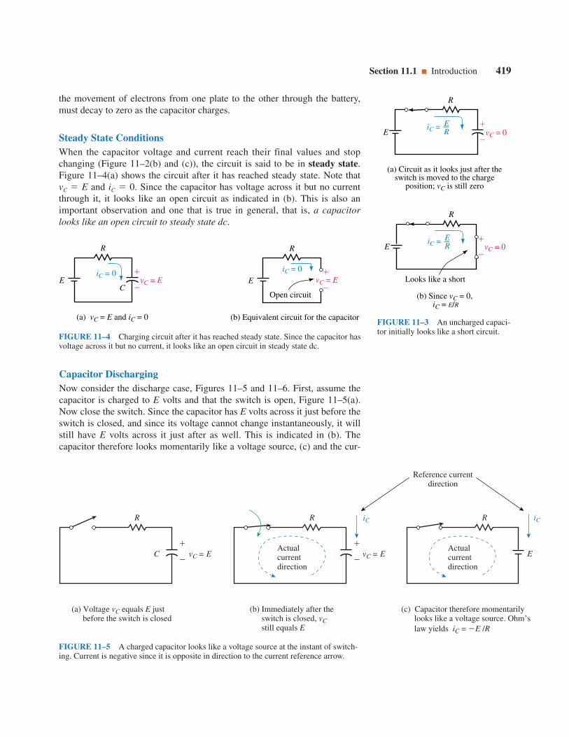
Steady State ConditionsWhen the capacitor voltage and current reach their final values and stopchanging (Figure 11–2(b) and (c)), the circuit is said to be in steady state.Figure 11–4(a) shows the circuit after it has reached steady state. Note thatvC E and iC 0. Since the capacitor has voltage across it but no currentthrough it, it looks like an open circuit as indicated in (b). This is also animportant observation and one that is true in general, that is, a capacitorlooks like an open circuit to steady state dc.
Section 11.1 Introduction 419
vC = 0
R
EER
iC =
(a) Circuit as it looks just after theswitch is moved to the charge
position; vC is still zero
(b) Since vC = 0, iC = E/R
vC = 0
R
EER
iC =
Looks like a short
FIGURE 11–3 An uncharged capaci-tor initially looks like a short circuit.
iC = 0E vC = E
R
C
(a) vC = E and iC = 0
iC = 0E vC = E
R
(b) Equivalent circuit for the capacitor
Open circuit
FIGURE 11–4 Charging circuit after it has reached steady state. Since the capacitor hasvoltage across it but no current, it looks like an open circuit in steady state dc.
Capacitor DischargingNow consider the discharge case, Figures 11–5 and 11–6. First, assume thecapacitor is charged to E volts and that the switch is open, Figure 11–5(a).Now close the switch. Since the capacitor has E volts across it just before theswitch is closed, and since its voltage cannot change instantaneously, it willstill have E volts across it just after as well. This is indicated in (b). Thecapacitor therefore looks momentarily like a voltage source, (c) and the cur-
R
C vC = E
R
vC = E
iC
Actualcurrentdirection
Reference currentdirection
R
E
iC
Actualcurrentdirection
(a) Voltage vC equals E justbefore the switch is closed
(b) Immediately after theswitch is closed, vC still equals E
(c) Capacitor therefore momentarily looks like a voltage source. Ohm’s
law yields iC = E /R
FIGURE 11–5 A charged capacitor looks like a voltage source at the instant of switch-ing. Current is negative since it is opposite in direction to the current reference arrow.

rent thus jumps immediately to E/R amps. (Note that the current is nega-tive since it is opposite in direction to the reference arrow.) The voltage andcurrent then decay to zero as indicated in Figure 11–6.
420 Chapter 11 Capacitor Charging, Discharging, and Simple Waveshaping Circuits
t
vC
E
0
(a)
(b)
iC
ER
t0
FIGURE 11–6 Voltage and currentduring discharge. Time t 0 s isdefined as the instant the switch ismoved to the discharge position.
EXAMPLE 11–1 For Figure 11–1, E 40 V, R 10 , and the capacitor isinitially uncharged. The switch is moved to the charge position and the capac-itor allowed to charge fully. Then the switch is moved to the discharge posi-tion and the capacitor allowed to discharge fully. Sketch the voltages and cur-rents and determine the values at switching and in steady state.
Solution The current and voltage curves are shown in Figure 11–7. Initially,i 0 A since the switch is open. Immediately after it is moved to the chargeposition, the current jumps to E/R 40 V/10 4 A; then it decays to zero.At the same time, vC starts at 0 V and climbs to 40 V. When the switch ismoved to the discharge position, the capacitor looks momentarily like a 40-Vsource and the current jumps to 40 V/10 4 A; then it decays to zero.At the same time, vC also decays to zero.
t
iC
(b) Note the circuit that is valid during each time interval
10
iC vC
10
iC vC
Chargephase
Dischargephase
4 A
4 A
t
vC
0 V 0 V
40 V
0
0
40 V
(a)
0 A 0 A0 A
FIGURE 11–7 A charge/discharge example.

The Meaning of Time in Transient AnalysisThe time t used in transient analysis is measured from the instant of switch-ing. Thus, t 0 in Figure 11–2 is defined as the instant the switch is movedto charge, while in Figure 11–6, it is defined as the instant the switch ismoved to discharge. Voltages and currents are then represented in terms ofthis time as vC(t) and iC(t). For example, the voltage across a capacitor at t 0 s is denoted as vC(0), while the voltage at t 10 ms is denoted as vC (10ms), and so on.
A problem arises when a quantity is discontinuous as is the current ofFigure 11–2(c). Since its value is changing at t 0 s, iC (0) cannot bedefined. To get around this problem, we define two values for 0 s. Wedefine t 0 s as t 0 s just prior to switching and t 0 s as t 0 s justafter switching. In Figure 11–2(c), therefore, iC(0) 0 A while iC (0) E/R amps. For Figure 11–6, iC (0) 0 A and iC (0) E/R amps.
Exponential FunctionsAs we will soon show, the waveforms of Figures 11–2 and 11–6 are expo-nential and vary according to ex or (1 ex), where e is the base of the nat-ural logarithm. Fortunately, exponential functions are easy to evaluate withmodern calculators using their ex function. You will need to be able to evalu-ate both ex and (1 ex) for any value of x. Table 11–1 shows a tabulationof values for both cases. Note that as x gets larger, ex gets smaller andapproaches zero, while (1 ex) gets larger and approaches 1. These obser-vations will be important to you in what follows.
Section 11.1 Introduction 421
PRACTICAL NOTES...Some key points to remember are the following:
1. Capacitor voltage cannot change instantaneously, but current can.
2. To determine currents and voltages in a circuit at the instant of switching,replace uncharged capacitors with short circuits and charged capacitorswith dc sources equal to their respective voltages at the instant of switching.
3. To determine currents and voltages in a dc circuit after it has reachedsteady state, replace capacitors with open circuits.
4. For both the charging and discharging cases, show capacitor current iC
such that the plus sign for vC is at the tail of the current reference arrow.For charging, you will find that current is in the same direction as iC andhence is positive, while for discharging, current is opposite in direction toiC and hence is negative.
PRACTICEPROBLEMS 1
1. Use your calculator and verify the entries in Table 11–1. Be sure to changethe sign of x before using the e x function. Note that e0 e0 1 since anyquantity raised to the zeroth power is one.
2. Plot the computed values on graph paper and verify that they yield curves thatlook like those shown in Figure 11–2(b) and (c).
TABLE 11–1 Table of Exponentials
x ex 1 ex
0 1 01 0.3679 0.63212 0.1353 0.86473 0.0498 0.95024 0.0183 0.98175 0.0067 0.9933
11.2 Capacitor Charging EquationsWe will now develop equations for voltages and current during charging.Consider Figure 11–8. KVL yields
vR vC E (11–1)
But vR RiC and iC CdvC /dt (Equation 10–20). Thus, vR RCdvC /dt. Sub-stituting this into Equation 11–1 yields
RCd
d
v
tC
vC E (11–2)
Equation 11–2 can be solved for vC using basic calculus (see ). The result is
vC E(1 et/RC) (11–3)
where R is in ohms, C is in farads, t is in seconds and et/RC is the exponen-tial function discussed earlier. The product RC has units of seconds. (This isleft as an exercise for the student to show.)
Solving Equation 11–2 (Optional Derivation)First, rearrange Equation 11–2:
d
d
v
tC
R
1
C(E vC)
Rearrange again:
E
d
vC
vC
R
d
C
t
Now multiply both sides by 1 and integrate.
vC
0vC
d
vC
E
R
1
C t
0dt
ln(vC E)0
vC
RtC
0
t
Next, substitute integration limits,
ln(vC E) ln(E) RtC
lnvC
E
E
R
t
C
Finally, take the inverse log of both sides. Thus,
vC
E
E et/RC
When you rearrange this, you get Equation 11–3. That is,
vC E(1 et/RC )
∫
422 Chapter 11 Capacitor Charging, Discharging, and Simple Waveshaping Circuits
iCE vC
vR
FIGURE 11–8 Circuit for the charg-ing case. Capacitor is initiallyuncharged.
∫

Now consider the resistor voltage. From Equation 11–1, vR E vC.Substituting vC from Equation 11–3 yields vR E E(1 et/RC) E E Eet/RC. After cancellation, you get
vR Eet/RC (11–4)
Now divide both sides by R. Since iC iR vR/R, this yields
iC ER
et/RC (11–5)
The waveforms are shown in Figure 11–9. Values at any time may be deter-mined by substitution.
Section 11.2 Capacitor Charging Equations 423
t
vC
E
0
vC = E (1e )
t
vR
E
0
t / RC
vR = E e t / RC
t
iC
0
iC = e t / RCERE
R
FIGURE 11–9 Curves for the circuitof Figure 11–8.
EXAMPLE 11–2 Suppose E 100 V, R 10 k, and C 10 mF:
a. Determine the expression for vC.
b. Determine the expression for iC.
c. Compute the capacitor voltage at t 150 ms.
d. Compute the capacitor current at t 150 ms.
e. Locate the computed points on the curves.
Solutiona. RC (10 103 )(10 106 F) 0.1 s. From Equation 11–3, vC
E(1 et/RC) 100(1 et/0.1) 100(1 e10 t) V.
b. From Equation 11–5, iC (E/R)et/RC (100 V/10 k)e10 t 10e10 t mA.
c. At t 0.15 s, vC 100(1 e10 t) 100(1 e10(0.15)) 100(1 e1.5) 100(1 0.223) 77.7 V.
d. iC 10e10 t mA 10e10(0.15) mA 10e1.5 mA 2.23 mA.
e. The corresponding points are shown in Figure 11–10.
t (ms)
vC
100 V
1500
(a)
77.7 V
vC = 100 (1e )V10t
t (ms)
iC
10 mA
1500
(b)
2.23 mA
iC = 10 e mA10t
In the above example, we expressed voltage as vC 100(1 et/0.1) andas 100(1 e10t ) V. Similarly, current can be expressed as iC 10et/0.1 or as10e10t mA. Although some authors prefer one notation over the other, bothare correct and we will use them interchangeably.
EWB FIGURE 11–10 The computed points plotted on the vC and iC curves.

Answers:1. 2. 80(1 e50t) V 20e50t mA
424 Chapter 11 Capacitor Charging, Discharging, and Simple Waveshaping Circuits
PRACTICEPROBLEMS 2
1. Determine additional voltage and current points for Figure 11–10 by comput-ing values of vC and iC at values of time from t 0 s to t 500 ms at 100-msintervals. Plot the results.
2. The switch of Figure 11–11 is closed at t 0 s. If E 80 V, R 4 k, andC 5 mF, determine expressions for vC and iC. Plot the results from t 0 s tot 100 ms at 20-ms intervals. Note that charging takes less time here thanfor Problem 1.
E C vC
iC
R
FIGURE 11–11
t(ms) vC(V) iC(mA)
0 0 10100 63.2 3.68200 86.5 1.35300 95.0 0.498400 98.2 0.183500 99.3 0.067
t(ms) vC(V) iC(mA)
0 0 2020 50.6 7.3640 69.2 2.7060 76.0 0.99680 78.6 0.366
100 79.4 0.135
EXAMPLE 11–3 For the circuit of Figure 11–11, E 60 V, R 2 k, andC 25 mF. The switch is closed at t 0 s, opened 40 ms later and left open.Determine equations for capacitor voltage and current and plot.
Solution RC (2 k)(25 mF) 50 ms. As long as the switch is closed(i.e., from t 0 s to 40 ms), the following equations hold:
vC E(1 et/RC) 60(1 et/50 ms) V
iC (E/R)et/RC 30et/50 ms mA
Voltage starts at 0 V and rises exponentially. At t 40 ms, the switch isopened, interrupting charging. At this instant, vC 60(1 e(40/50)) 60(1 e0.8) 33.0 V. Since the switch is left open, the voltage remains constant at33 V thereafter as indicated in Figure 11–12. (The dotted curve shows howthe voltage would have kept rising if the switch had remained closed.)
Now consider current. The current starts at 30 mA and decays to iC 30e(40/50) mA 13.5 mA at t 40 ms. At this point, the switch is opened,and the current drops instantly to zero. (The dotted line shows how the cur-rent would have decayed if the switch had not been opened.)

The Time ConstantThe rate at which a capacitor charges depends on the product of R and C.This product is known as the time constant of the circuit and is given thesymbol t (the Greek letter tau). As noted earlier, RC has units of seconds.Thus,
t RC (seconds, s) (11–6)
Using t, Equations 11–3 to 11–5 can be written as
vC E(1 et/t) (11–7)
iC ER
et/t (11–8)
and
vR Eet/t (11–9)
Duration of a TransientThe length of time that a transient lasts depends on the exponential func-tion et/t. As t increases, et/t decreases, and when it reaches zero, the tran-sient is gone. Theoretically, this takes infinite time. In practice, however,over 99% of the transition takes place during the first five time constants(i.e., transients are within 1% of their final value at t 5 t). This can beverified by direct substitution. At t 5 t, vC E(1 et/t) E(1 e5) E(1 0.0067) 0.993E, meaning that the transient has achieved 99.3% ofits final value. Similarly, the current falls to within 1% of its final value infive time constants. Thus, for all practical purposes, transients can be con-sidered to last for only five time constants (Figure 11–13). Figure 11–14summarizes how transient voltages and currents are affected by the timeconstant of a circuit—the larger the time constant, the longer the durationof the transient.
Section 11.2 Capacitor Charging Equations 425
t (ms)
vC
60 V
Capacitor voltagestops changing when
the switch opens.
0 40
33 V
(a)
t (ms)
iC (mA)
30Current drops
to zero.
0 40
13.5
(b)
t
vC
iC or vR
05
FIGURE 11–13 Transients last fivetime constants.
EWB FIGURE 11–12 Incomplete charging. The switch of Figure 11–11 wasopened at t 40 ms, causing charging to cease.

Figure 11–15 shows percent capacitor voltage and current plotted versusmultiples of time constant. (Points are computed from vC 100(1 et/t)and iC 100et/t. For example, at t t, vC 100(1 et/t) 100(1 et/t) 100(1 e1) 63.2 V, i.e., 63.2%, and iC 100et/t 100e1 36.8 A, which is 36.8%, and so on.) These curves, referred to as universaltime constant curves, provide an easy method to determine voltages and cur-rents with a minimum of computation.
426 Chapter 11 Capacitor Charging, Discharging, and Simple Waveshaping Circuits
t increasing
vC
(a)
t
increasing
iC
(b)
FIGURE 11–14 Illustrating how voltage and current in an RC circuit are affected by itstime constant. The larger the time constant, the longer the capacitor takes to charge.
EXAMPLE 11–4 For the circuit of Figure 11–11, how long will it take forthe capacitor to charge if R 2 k and C 10 mF?
Solution t RC (2 k)(10 mF) 20 ms. Therefore, the capacitorcharges in 5 t 100 ms.
EXAMPLE 11–5 The transient in a circuit with C 40 mF lasts 0.5 s. Whatis R?
Solution 5 t 0.5 s. Thus, t 0.1 s and R t/C 0.1 s/(40 106 F) 2.5 k.
t
vC
60%
40%50%
70%80%90%
100%
30%20%
0
10%0%
2 3 4 5
Perc
ent o
f Fu
ll V
olta
ge
95.0%
86.5%
63.2%
99.3%
98.2%
(a)
t
iC or vR
60%
40%50%
70%80%90%
100%
30%20%
0
10%0%
2 3 4 5
Perc
ent
36.8%
100%
4.98%
13.5%
1.83%
0.67%
(b)
FIGURE 11–15 Universal voltage and current curves for RC circuit.

2. Given iC 50e20t mA.
a. What is t?
b. Compute the current at t 0 s, 25 ms, 50 ms, 75 ms, 100 ms, and 500 msand sketch it.
3. Given vC 100(1 e50t) V, compute vC at the same time intervals as inProblem 2 and sketch.
4. For Figure 11–16, determine expressions for vC and iC. Compute capacitorvoltage and current at t 0.6 s.
5. Refer to Figure 11–10:
a. What are vC(0) and vC(0)?
b. What are iC(0) and iC(0)?
c. What are the steady state voltage and current?
6. For the circuit of Figure 11–11, the current just after the switch is closed is2 mA. The transient lasts 40 ms and the capacitor charges to 80 V. DetermineE, R, and C.
7. Find capacitor voltage and current for Figure 11–16 at t 0.6 s using the uni-versal time constant curves of Figure 11–15.
(Answers are at the end of the chapter.)
Section 11.3 Capacitor with an Initial Voltage 427
EXAMPLE 11–6 Using Figure 11–15, compute vC and iC at two time con-stants into charge for a circuit with E 25 V, R 5 k, and C 4 mF. Whatis the corresponding value of time?
Solution At t 2 t, vC equals 86.5% of E or 0.865(25 V) 21.6 V. Simi-larly, iC 0.135I0 0.135(E/R) 0.675 mA. These values occur at t 2 t 2RC 40 ms.
IN-PROCESSLEARNINGCHECK 1
1. If the capacitor of Figure 11–16 is uncharged, what is the current immedi-ately after closing the switch?
E C vC
iC
R = 200
40 V
C = 1000 F
FIGURE 11–16
11.3 Capacitor with an Initial VoltageSuppose a previously charged capacitor has not been discharged and thusstill has voltage on it. Let this voltage be denoted as V0. If the capacitor isnow placed in a circuit like that in Figure 11–16, the voltage and current
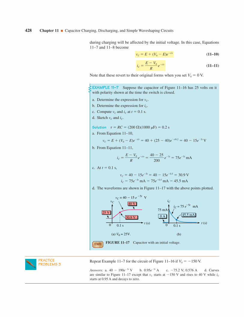
during charging will be affected by the initial voltage. In this case, Equations11–7 and 11–8 become
vC E (V0 E)et/t (11–10)
iC E
R
V0 et/t (11–11)
Note that these revert to their original forms when you set V0 0 V.
428 Chapter 11 Capacitor Charging, Discharging, and Simple Waveshaping Circuits
EXAMPLE 11–7 Suppose the capacitor of Figure 11–16 has 25 volts on itwith polarity shown at the time the switch is closed.
a. Determine the expression for vC.
b. Determine the expression for iC.
c. Compute vC and iC at t 0.1 s.
d. Sketch vC and iC.
Solution t RC (200 )(1000 mF) 0.2 s
a. From Equation 11–10,
vC E (V0 E)et/t 40 (25 40)et/0.2 40 15e5t V
b. From Equation 11–11,
iC E
R
V0et/t
40
2
00
25 e5t 75e5t mA
c. At t 0.1 s,
vC 40 15e5t 40 15e0.5 30.9 V
iC 75e5t mA 75e0.5 mA 45.5 mA
d. The waveforms are shown in Figure 11–17 with the above points plotted.
t (s)
vC
0
(a) V0 = 25V.
30.9 V
40 V
25 V
vC = 40 15 e V5t
0.1 st (s)
iC
75 mA
0.1 s0
(b)
45.5 mA0 A
iC = 75 e mA5t
PRACTICEPROBLEMS 3
Repeat Example 11–7 for the circuit of Figure 11–16 if V0 150 V.
Answers: a. 40 190e5t V b. 0.95e5t A c. 75.2 V; 0.576 A d. Curvesare similar to Figure 11–17 except that vC starts at 150 V and rises to 40 V while iC
starts at 0.95 A and decays to zero.
EWB FIGURE 11–17 Capacitor with an initial voltage.
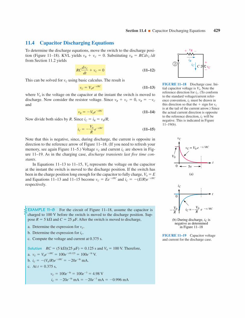
11.4 Capacitor Discharging EquationsTo determine the discharge equations, move the switch to the discharge posi-tion (Figure 11–18). KVL yields vR vC 0. Substituting vR RCdvC /dtfrom Section 11.2 yields
RCd
d
v
tC
vC 0 (11–12)
This can be solved for vC using basic calculus. The result is
vC V0et/RC (11–13)
where V0 is the voltage on the capacitor at the instant the switch is moved todischarge. Now consider the resistor voltage. Since vR vC 0, vR vC
and
vR V0et/RC (11–14)
Now divide both sides by R. Since iC iR vR/R,
iC V
R0
et/RC (11–15)
Note that this is negative, since, during discharge, the current is opposite indirection to the reference arrow of Figure 11–18. (If you need to refresh yourmemory, see again Figure 11–5.) Voltage vC and current iC are shown in Fig-ure 11–19. As in the charging case, discharge transients last five time con-stants.
In Equations 11–13 to 11–15, V0 represents the voltage on the capacitorat the instant the switch is moved to the discharge position. If the switch hasbeen in the charge position long enough for the capacitor to fully charge, V0 Eand Equations 11–13 and 11–15 become vC Eet/RC and iC (E/R)et/RC
respectively.
Section 11.4 Capacitor Discharging Equations 429
vC
C
iRiC
vR
2
FIGURE 11–18 Discharge case. Ini-tial capacitor voltage is V0. Note thereference direction for iC. (To conformto the standard voltage/current refer-ence convention, iC must be drawn inthis direction so that the sign for vC
is at the tail of the current arrow.) Sincethe actual current direction is oppositeto the reference direction, iC will benegative. This is indicated in Figure11–19(b).
t
vC
V0
5
t
iC
iC = e
(b) During discharge, iC isnegative as determined
in Figure 11–18
(a)
V0
R V0 R
t / RC
vC = V0 e t / RC
0
0
FIGURE 11–19 Capacitor voltageand current for the discharge case.
EXAMPLE 11–8 For the circuit of Figure 11–18, assume the capacitor ischarged to 100 V before the switch is moved to the discharge position. Sup-pose R 5 k and C 25 mF. After the switch is moved to discharge,
a. Determine the expression for vC.
b. Determine the expression for iC.
c. Compute the voltage and current at 0.375 s.
Solution RC (5 k)(25 mF) 0.125 s and V0 100 V. Therefore,
a. vC V0et/RC 100et/0.125 100e8t V.
b. iC (V0/R)et/RC 20e8t mA.
c. At t 0.375 s,
vC 100e8t 100e3 4.98 V
iC 20e8t mA 20e3 mA 0.996 mA

The universal time constant curve of Figure 11–15(b) may also be usedto solve discharge problems. For example, for the circuit of Example 11–8,at t 3 t, capacitor voltage has fallen to 4.98% of E, which is (0.0498)(100V) 4.98 V and current has decayed to 4.98% of 20 mA which is(0.0498)(20 mA) 0.996 mA. (These agree with Example 11–8 since3 t was also the value of time used there.)
11.5 More Complex CircuitsThe charge and discharge equations described previously apply only to cir-cuits of the forms shown in Figures 11–2 and 11–5 respectively. Fortu-nately, many circuits can be reduced to these forms using standard circuitreduction techniques such as series and parallel combinations, source con-versions, Thévenin’s theorem, and so on. Once a circuit has been reducedto its series equivalent, you can use any of the equations that we havedeveloped so far.
430 Chapter 11 Capacitor Charging, Discharging, and Simple Waveshaping Circuits
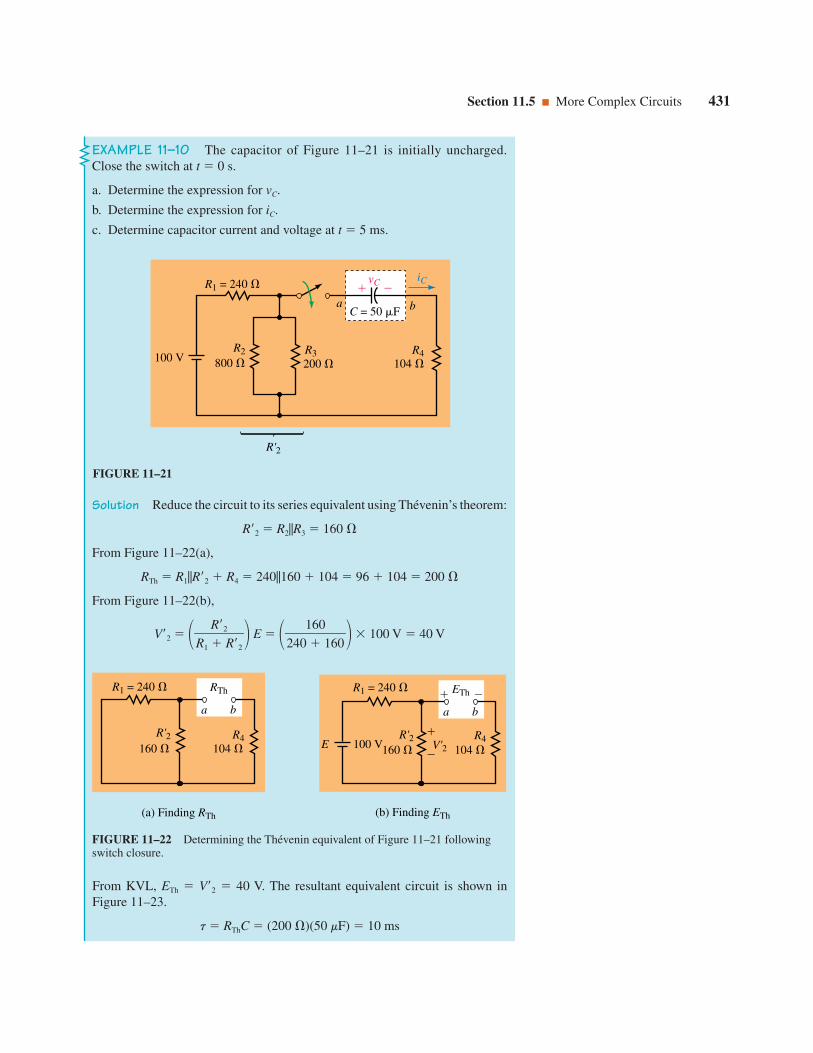
EXAMPLE 11–9 For the circuit of Figure 11–20(a), determine expressionsfor vC and iC. Capacitors are initially uncharged.
Solution Reduce circuit (a) to circuit (b).
Req R1R2 2.0 k; Ceq C1 C2 10 mF.
ReqCeq (2 k)(10 106 F) 0.020 s
Thus,
vC E(1 et/ReqCeq) 100(1 et/0.02) 100(1 e50t) V
iC RE
eq
et/ReqCeq 2100000
et/0.02 50 e50t mA
E
iC
100 V
R2 = 6 k
R1 = 3 k
vC
C2
(a)
2 FC1
8 F
E
iC
100 V
Req = 2 k
vC
Ceq = 10 F
(b)
FIGURE 11–20
Section 11.5 More Complex Circuits 431
EXAMPLE 11–10 The capacitor of Figure 11–21 is initially uncharged.Close the switch at t 0 s.
a. Determine the expression for vC.
b. Determine the expression for iC.
c. Determine capacitor current and voltage at t 5 ms.
Solution Reduce the circuit to its series equivalent using Thévenin’s theorem:
R2 R2R3 160
From Figure 11–22(a),
RTh R1R2 R4 240160 104 96 104 200
From Figure 11–22(b),
V2 R1
R
2
R2
E 240
1
60
160 100 V 40 V
100 V
R1 = 240
C = 50 F
R4
vC
104 R3200
R2
R'2
800
a b
iC
FIGURE 11–21
R1 = 240
R4
RTh
104 R'2
160
a b
(a) Finding RTh
100 VE V'2
R1 = 240
R4
ETh
104 R'2
160
a b
(b) Finding ETh
FIGURE 11–22 Determining the Thévenin equivalent of Figure 11–21 followingswitch closure.
From KVL, ETh V2 40 V. The resultant equivalent circuit is shown inFigure 11–23.
t RThC (200 )(50 mF) 10 ms

432 Chapter 11 Capacitor Charging, Discharging, and Simple Waveshaping Circuits
a. vC ETh(1 et/t) 40(1 e100t) V
b. iC E
RT
T
h
h
et/t 2
4
0
0
0et/0.01 200e100t mA
c. iC 200e100(5 ms) 121 mA. Similarly, vC 15.7 V
RTh = 200 iC
ETh 40 V 50 F vC
FIGURE 11–23 The Thévenin equivalent of Figure 11–21.
PRACTICEPROBLEMS 4
1. For Figure 11–21, if R1 400 , R2 1200 , R3 300 , R4 50 , C 20 mF, and E 200 V, determine vC and iC.
2. Using the values shown in Figure 11–21, determine vC and iC if the capacitorhas an initial voltage of 60 V.
3. Using the values of Problem 1, determine vC and iC if the capacitor has an ini-tial voltage of 50 V.
Answers:1. 75(1 e250t) V; 0.375e250t A
2. 40 20e100t V; 0.1e100t A
3. 75 125e250t V; 0.625e250t A
PRACTICAL NOTES...
Notes About Time References
1. So far, we have dealt with charging and discharging problems separately.For these, we define t 0 s as the instant the switch is moved to thecharge position for charging problems and to the discharge position fordischarging problems.
2. When you have both charge and discharge cases in the same example, youneed to establish clearly what you mean by “time.” We use the followingprocedure:
a. Define t 0 s as the instant the switch is moved to the first position,then determine corresponding expressions for vC and iC. These expres-sions and the corresponding time scale are valid until the switch ismoved to its new position.
b. When the switch is moved to its new position, shift the time referenceand make t 0 s the time at which the switch is moved to its new

Section 11.5 More Complex Circuits 433
position, then determine corresponding expressions for vC and iC. Thesenew expressions are only valid from the new t 0 s reference point.The old expressions are valid only on the old time scale.
c. We now have two time scales for the same graph. However, we gener-ally only show the first scale explicitly; the second scale is impliedrather than shown.
d. Use tC to represent the time constant for charging and td to representthe time constant for discharging. Since the equivalent resistance andcapacitance for discharging may be different than that for charging, thetime constants may be different for the two cases.
EXAMPLE 11–11 The capacitor of Figure 11–24(a) is uncharged. Theswitch is moved to position 1 for 10 ms, then to position 2, where it remains.
a. Determine vC during charge.
b. Determine iC during charge.
c. Determine vC during discharge.
d. Determine iC during discharge.
e. Sketch the charge and discharge waveforms.
Solution Figure 11–24(b) shows the equivalent charging circuit. Here,
tc (R1 R2)C (1 k)(2 mF) 2.0 ms.
(a) Full circuit
R1
R3
iC
100 V 2 F vC
2
1
800
R2
200
300
(b) Charging circuit
RTc = 1000
iC
100 V 2 F vC
vC
2 F
iC
500
(c) Discharging circuitV0 = 100 V at t = 0 s
FIGURE 11–24
When solving a transient prob-lem, always draw the circuit as itlooks during each time intervalof interest. (It doesn’t take longto do this, and it helps clarifyjust what it is you need to lookat for each part of the solution.)This is illustrated in Example11–11. Here, we have drawn thecircuit in Figure 11–24(b) as itlooks during charging and in (c)as it looks during discharging. Itis now clear which componentsare relevant to the charging phaseand which are relevant to the dis-charging phase.
NOTES…

434 Chapter 11 Capacitor Charging, Discharging, and Simple Waveshaping Circuits
a. vC E(1 et/tc) 100(1 e500t) V
b. iC RE
Tc
et/tc 1100000
e500t 100e500t mA
Since 5tc 10 ms, charging is complete by the time the switch is moved todischarge. Thus, V0 100 V when discharging begins.
c. Figure 11–24(c) shows the equivalent discharge circuit. Note V0 100 V.
td (500 )(2 mF) 1.0 ms
vC V0et/td 100e1000t V
where t 0 s has been redefined for discharge as noted above.
d. iC R2
V
0
R3
et/td 1
5
0
0
0
0e1000t 200e1000t mA
e. See Figure 11–25. Note that discharge is more rapid than charge sincetd tc.
vC (V)
0 2 4 6 8
100
10 12 14t (ms)
5c
(a)
02 4 6 8
100
100
200
10 14t (ms)
iC (mA)
(b)
FIGURE 11–25 Waveforms for the circuit of Figure 11–24. Note that td is shorterthan tc.
EXAMPLE 11–12 The capacitor of Figure 11–26 is uncharged. The switchis moved to position 1 for 5 ms, then to position 2 and left there.
E1E2
iC
10 V 4 F vC
2
1 1000
30 V
a. Determine vC while the switch is in position 1.
b. Determine iC while the switch is in position 1.
c. Compute vC and iC at t 5 ms.
EWB FIGURE 11–26

Section 11.5 More Complex Circuits 435
d. Determine vC while the switch is in position 2.
e. Determine iC while the switch is in position 2.
f. Sketch the voltage and current waveforms.
g. Determine vC and iC at t 10 ms.
Solution
tc td RC (1 k)(4 mF) 4 ms
a. vC E1(1 et/tc) 10(1 e250t) V
b. iC E
R1
et/tc 1
1
0
0
00e250t 10e250t mA
c. At t 5 ms,
vC 10(1 e250 0.005) 7.14 V
iC 10e250 0.005 mA 2.87 mA
d. In position 2, E2 30 V, and V0 7.14 V. Use Equation 11–10:
vC E2 (V0 E2)et/td 30 (7.14 30)e250t
30 22.86e250t V
where t 0 s has been redefined for position 2.
e. iC E2
R
V0 et/td
30
1
00
7
0
.14e250t 22.86e250t mA
f. See Figure 11–27.
g. t 10 ms is 5 ms into the new time scale. Thus, vC 30 22.86e250(5 ms) 23.5 V and iC 22.86e250(5 ms) 6.55 mA. Values are plotted on thegraph.
t (ms)
30
vC (V)
20
10
0 5 10 15
23.5 V
7.14 V
t (ms)
15
iC (mA)
2025
105
0 5 10 15
22.86 mA
2.87 mA
6.55 mA
FIGURE 11–27 Capacitor voltage and current for the circuit of Figure 11–26.
EXAMPLE 11–13 In Figure 11–28(a), the capacitor is initially uncharged.The switch is moved to the charge position, then to the discharge position,yielding the current shown in (b). The capacitor discharges in 1.75 ms. Deter-mine the following:
a. E. b. R1. c. C.

RC Circuits in Steady State DCWhen an RC circuit reaches steady state dc, its capacitors look like open cir-cuits. Thus, a transient analysis is not needed.
436 Chapter 11 Capacitor Charging, Discharging, and Simple Waveshaping Circuits
Solutiona. Since the capacitor charges fully, it has a value of E volts when switched
to discharge. The discharge current spike is therefore
10
E25 3 A
Thus, E 105 V.
b. The charging current spike has a value of
10
E R1
7 A
Since E 105 V, this yields R1 5 .
c. 5 td 1.75 ms. Therefore td 350 ms. But td (R2 R3)C. Thus, C 350 ms/35 10 mF.
(a)
R1 R3 = 10
R2 25
iC
E
2
1
C
(b)
3
7
0t (s)
iC (A)
Fully chargedhere
FIGURE 11–28
EXAMPLE 11–14 The circuit of Figure 11–29(a) has reached steady state.Determine the capacitor voltages.
(a)
40
8 12
40 90 V
60
V1
V2
200 V
100 F
20 F
EWB FIGURE 11–29 Continues

Section 11.5 More Complex Circuits 437
PRACTICEPROBLEMS 5
1. The capacitor of Figure 11–30(a) is initially unchanged. At t 0 s, the switchis moved to position 1 and 100 ms later, to position 2. Determine vC and iC forposition 2.
2. Repeat for Figure 11–30(b). Hint: Use Thévenin’s theorem.
Solution Replace all capacitors with open circuits. Thus,
I1 40
20
0 V60 2 A, I2 1.5 A
KVL: V1 120 18 0. Therefore, V1 138 V. Further,
V2 (8 )(1.5 A) 12 V
90 V40 8 12
(b)
40
8 12
40 90 V
60
I1
V1
120 V200 V 18 V 12 V
I2
V2
I1 = 2 A I2 = 1.5 A
EWB FIGURE 11–29 Continued
40
30 80
20
vC
20 V
1
2iC
1 k
4 k2 mA2 k
12 V
1
2
iC
vC
(b) C = 20 F
(a) C = 500 F
FIGURE 11–30
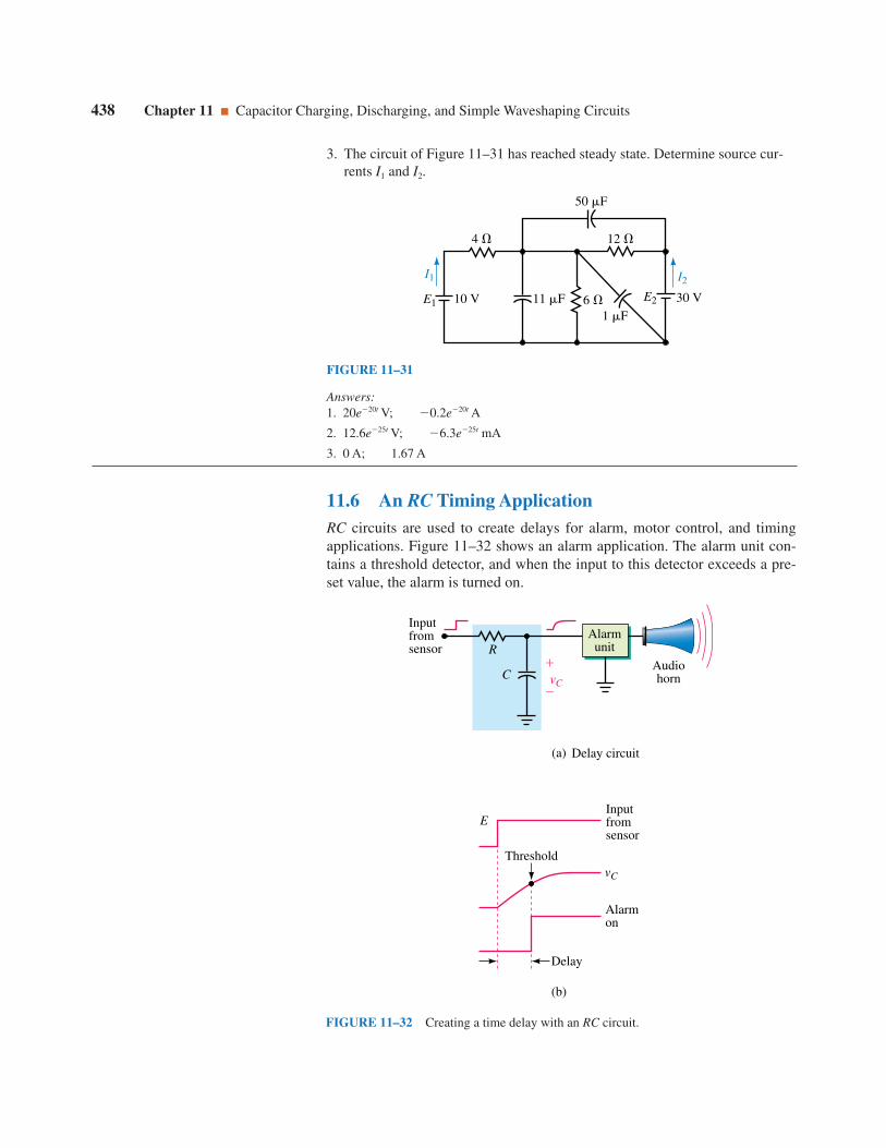
3. The circuit of Figure 11–31 has reached steady state. Determine source cur-rents I1 and I2.
438 Chapter 11 Capacitor Charging, Discharging, and Simple Waveshaping Circuits
10 V
4
6 30 V11 F1 F
50 F
12
I2I1
E2E1
FIGURE 11–31
Answers:1. 20e20t V; 0.2e20t A
2. 12.6e25t V; 6.3e25t mA
3. 0 A; 1.67 A
11.6 An RC Timing ApplicationRC circuits are used to create delays for alarm, motor control, and timingapplications. Figure 11–32 shows an alarm application. The alarm unit con-tains a threshold detector, and when the input to this detector exceeds a pre-set value, the alarm is turned on.
vC
E
Delay
Threshold
Alarmon
Inputfromsensor
vC
R
C
Delay circuit
Inputfromsensor
Audiohorn
Alarmunit
(a)
(b)
FIGURE 11–32 Creating a time delay with an RC circuit.

Section 11.6 An RC Timing Application 439
EXAMPLE 11–15 The circuit of Figure 11–32 is part of a building securitysystem. When an armed door is opened, you have a specified number of sec-onds to disarm the system before the alarm goes off. If E 20 V, C 40 mF,the alarm is activated when vC reaches 16 V, and you want a delay of at least25 s, what value of R is needed?
Solution vC E(1 et/RC). After a bit of manipulation, you get
et/RC E
E
vC
Taking the natural log of both sides yields
R
t
C lnE
E
vC
At t 25 s, vC 16 V. Thus,
RtC ln20
2
016
ln 0.2 1.6094
Substituting t 25 s and C 40 mF yields
R 1.60
t94C 388 k
Choose the next higher standard value, namely 390 k.
25 s1.6094 40 106
EWB
PRACTICEPROBLEMS 6
1. Suppose you want to increase the disarm time of Example 11–15 to at least35 s. Compute the new value of R.
2. If, in Example 11–15, the threshold is 15 V and R 1 M, what is the dis-arm time?
Answers:1. 544 k. Use 560 k.
2. 55.5 s
IN-PROCESSLEARNINGCHECK 2
1. Refer to Figure 11–16:
a. Determine the expression for vC when V0 80 V. Sketch vC.
b. Repeat (a) if V0 40 V. Why is there no transient?
c. Repeat (a) if V0 60 V.
2. For Part (c) of Question 1, vC starts at 60 V and climbs to 40 V. Determineat what time vC passes through 0 V, using the technique of Example 11–15.
3. For the circuit of Figure 11–18, suppose R 10 k and C 10 mF:
a. Determine the expressions for vC and iC when V0 100 V. Sketch vC
and iC.
b. Repeat (a) if V0 100 V.
4. Repeat Example 11–12 if voltage source 2 is reversed, i.e., E2 30 V.

11.7 Pulse Response of RC CircuitsIn previous sections, we looked at the response of RC circuits to switched dcinputs. In this section, we consider the effect that RC circuits have on pulsewaveforms. Since many electronic devices and systems utilize pulse or rec-tangular waveforms, including computers, communications systems, andmotor control circuits, these are important considerations.
Pulse BasicsA pulse is a voltage or current that changes from one level to the other andback again as in Figure 11–34(a) and (b). A pulse train is a repetitive streamof pulses, as in (c). If a waveform’s high time equals its low time, as in (d), itis called a square wave.
The length of each cycle of a pulse train is termed its period, T, and thenumber of pulses per second is defined as its pulse repetition rate (PRR) orpulse repetition frequency (PRF). For example, in (e), there are two com-plete cycles in one second; therefore, the PRR 2 pulses/s. With two cyclesevery second, the time for one cycle is T 1⁄2 s. Note that this is 1/PRR.This is true in general. That is,
T PR
1R
s (11–16)
The width, tp, of a pulse relative to its period, [Figure 11–34(c)] is itsduty cycle. Thus,
duty cycle t
Tp 100% (11–17)
A square wave [Figure 11–34(d)] therefore has a 50% duty cycle, while awaveform with tp 1.5 ms and a period of 10 ms has a duty cycle of 15%.
440 Chapter 11 Capacitor Charging, Discharging, and Simple Waveshaping Circuits
(a)
iC vC
30
C = 1000 F
Circuit
(b) Norton equivalent
10 0.6 A
FIGURE 11–33 Hint: Use a source transformation.
(Answers are at the end of the chapter.)
5. The switch of Figure 11–33(a) is closed at t 0 s. The Norton equivalent ofthe circuit in the box is shown in (b). Determine expressions for vC and iC.The capacitor is initially uncharged.

In practice, waveforms are not ideal, that is, they do not change fromlow to high or high to low instantaneously. Instead, they have finite rise andfall times. Rise and fall times are denoted as tr and tf and are measuredbetween the 10% and 90% points as indicated in Figure 11–35(a). Pulsewidth is measured at the 50% point. The difference between a real wave-form and an ideal waveform is often slight. For example, rise and fall timesof real pulses may be only a few nanoseconds and when viewed on an oscil-loscope, as in Figure 11–35(b), appear to be ideal. In what follows, we willassume ideal waveforms.
Section 11.7 Pulse Response of RC Circuits 441
(c) Pulse train. T is referred to asthe period of the pulse train
tp
T
V
0T Time
(e) PRR = 2 pulses/s
T
1 s
T
(d) Square wave
T2
T
V
0
(b) Negative pulse
(a) Positive pulse
V
0Time
V
0Time
Time
FIGURE 11–34 Ideal pulses andpulse waveforms.
(a) Pulse definitions
90%
10%
90%
10%
tp
tr
Pulsewidth
Rise time Fall time
tf
(b) Pulse waveform viewed on an oscilloscope.
FIGURE 11–35 Practical pulse waveforms.
The Effect of Pulse WidthThe width of a pulse relative to a circuit’s time constant determines how it isaffected by an RC circuit. Consider Figure 11–36. In (a), the circuit has beendrawn to focus on the voltage across C; in (b), it has been drawn to focus onthe voltage across R. (Otherwise, the circuits are identical.) An easy way tovisualize the operation of these circuits is to assume that the pulse is gener-ated by a switch that is moved rapidly back and forth between V and com-mon as in (c). This alternately creates a charge and discharge circuit, andthus all of the ideas developed in this chapter apply directly.

442 Chapter 11 Capacitor Charging, Discharging, and Simple Waveshaping Circuits
(a) Output across C
vC
vin
R
C
(b) Output across R
vR
vin
C
V
(c) Modelling the pulse source
FIGURE 11–36 RC circuits with pulse input.
Pulse Width tp 5
First, consider the ouput of circuit (a). When the pulse width and timebetween pulses are very long compared with the circuit time constant, thecapacitor charges and discharges fully, Figure 11–37(b). (This case is similarto what we have already seen in this chapter.) Note, that charging and dis-charging occur at the transitions of the pulse. The transients thereforeincrease the rise and fall times of the output. In high-speed circuits, this maybe a problem. (You will learn more about this in your digital electronicscourses.)
Circuit (a)
T2
T2
vinV
0
vCV
05 5
Circuit (b)vRV
V
0
(a)
(b)
(c)
FIGURE 11–37 Pulse width muchgreater than 5 t. Note that the shadedareas indicate where the capacitor ischarging and discharging. Spikes occuron the input voltage transitions.
EXAMPLE 11–16 A square wave is applied to the input of Figure 11–36(a).If R 1 k and C 100 pF, estimate the rise and fall time of the output sig-nal using the universal time constant curve of Figure 11–15(a).
Solution Here, t RC (1 103)(100 1012) 100 ns. From Figure11–15(a), note that vC reaches the 10% point at about 0.1 t, which is (0.1)(100ns) 10 ns. The 90% point is reached at about 2.3 t, which is (2.3)(100 ns) 230 ns. The rise time is therefore approximately 230 ns 10 ns 220 ns. Thefall time will be the same.
Now consider the circuit in Figure 11–36(b). Here, current iC will besimilar to that of Figure 11–27(b), except that the pulse widths will be nar-rower. Since voltage vR R iC, the output will be a series of short, sharpspikes that occur at input transitions as in Figure 11–37(c). Under the condi-tions here (i.e., pulse width much greater than the circuit time constant), vR is
an approximation to the derivative of vin and the circuit is called a differen-tiator circuit. Such circuits have important practical uses.
Pulse Width tp 5
These waveforms are shown in Figure 11–38. Since the pulse width is 5t,the capacitor fully charges and discharges during each pulse. Thus wave-forms here will be similar to what we have seen previously.
Pulse Width tp 5
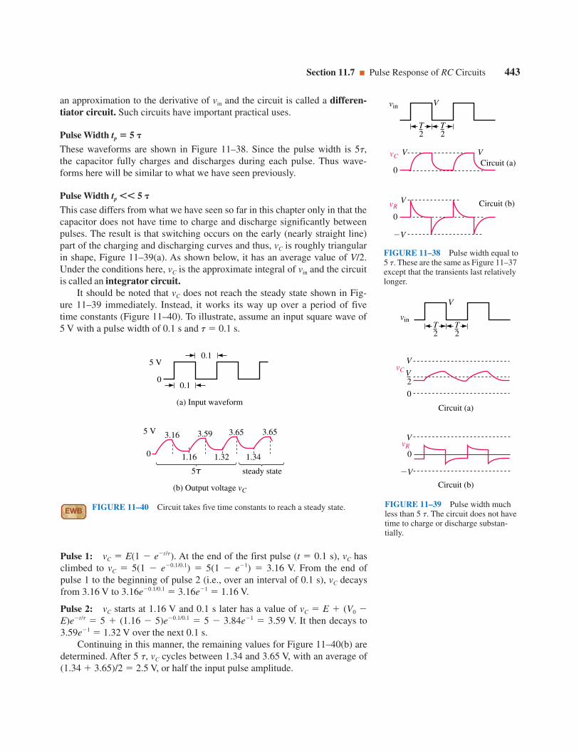
This case differs from what we have seen so far in this chapter only in that thecapacitor does not have time to charge and discharge significantly betweenpulses. The result is that switching occurs on the early (nearly straight line)part of the charging and discharging curves and thus, vC is roughly triangularin shape, Figure 11–39(a). As shown below, it has an average value of V/2.Under the conditions here, vC is the approximate integral of vin and the circuitis called an integrator circuit.
It should be noted that vC does not reach the steady state shown in Fig-ure 11–39 immediately. Instead, it works its way up over a period of fivetime constants (Figure 11–40). To illustrate, assume an input square wave of5 V with a pulse width of 0.1 s and t 0.1 s.
Section 11.7 Pulse Response of RC Circuits 443
Pulse 1: vC E(1 et/t). At the end of the first pulse (t 0.1 s), vC hasclimbed to vC 5(1 e0.1/0.1) 5(1 e1) 3.16 V. From the end ofpulse 1 to the beginning of pulse 2 (i.e., over an interval of 0.1 s), vC decaysfrom 3.16 V to 3.16e0.1/0.1 3.16e1 1.16 V.
Pulse 2: vC starts at 1.16 V and 0.1 s later has a value of vC E (V0 E)et/t 5 (1.16 5)e0.1/0.1 5 3.84e1 3.59 V. It then decays to3.59e1 1.32 V over the next 0.1 s.
Continuing in this manner, the remaining values for Figure 11–40(b) aredetermined. After 5 t, vC cycles between 1.34 and 3.65 V, with an average of(1.34 3.65)/2 2.5 V, or half the input pulse amplitude.
Circuit (a)
T2
T2
vin V
vC V V
0
Circuit (b)vRV
V
0
FIGURE 11–38 Pulse width equal to5 t. These are the same as Figure 11–37except that the transients last relativelylonger.
5 V
0
5 V 3.16
(b) Output voltage vC
(a) Input waveform
3.59
1.16
5τ steady state
1.32 1.34
3.65 3.65
00.1
0.1
EWB FIGURE 11–40 Circuit takes five time constants to reach a steady state.
Circuit (a)
T2
T2
vin
V
V 2
vCV
0
Circuit (b)
vRV
V
0
FIGURE 11–39 Pulse width muchless than 5 t. The circuit does not havetime to charge or discharge substan-tially.

444 Chapter 11 Capacitor Charging, Discharging, and Simple Waveshaping Circuits
PRACTICEPROBLEMS 7
Verify the remaining points of Figure 11–40(b).
Capacitive LoadingCapacitance occurs whenever conductors are separated by insulating mater-ial. This means that capacitance exists between wires in cables, betweentraces on printed circuit boards, and so on. In general, this capacitance isundesirable but it cannot be avoided. It is called stray capacitance. Fortu-nately, stray capacitance is often so small that it can be neglected. However,in high-speed circuits, it may cause problems.
To illustrate, consider Figure 11–41. The electronic driver of (a) pro-duces square pulses. However, when it drives a long line as in (b), straycapacitance loads it and increases the signal’s rise and fall times (sincecapacitance takes time to charge and discharge). If the rise and fall timesbecome excessively long, the signal reaching the load may be so degradedthat the system malfunctions. (Capacitive loading is a serious issue but wewill leave it for future courses to deal with.)
11.8 Transient Analysis Using ComputersElectronics Workbench and PSpice are well suited for studying transientsas they both incorporate easy to use graphing facilities that you can use toplot results directly on the screen. When plotting transients, you mustspecify the time scale for your plot—i.e., the length of time that youexpect the transient to last. A good value to start with is 5 t where t isthe time constant of the circuit. (For complex circuits, if you do not knowt, make an estimate, run a simulation, adjust the time scale, and repeatuntil you get an acceptable plot.)
Electronics WorkbenchWorkbench provides two ways to view waveforms—via its oscilloscope orvia its analysis graphing facility. Since the analysis graphing facility is easierto use and yields better output, we will begin with it. (In Chapter 14, weintroduce the oscilloscope.) As a first example, consider the RC charging cir-cuit of Figure 11–42. Determine capacitor voltage at t 50 ms and t 150ms. (You don’t need a switch; you simply tell Workbench to perform a tran-sient analysis.)Proceed as follows:
• Create the circuit of Figure 11–42 on the screen. (To display node number-ing, select Circuit/Schematic Options, enable Show Nodes, then click OK).
• Select Analysis/Transient and in the dialog box, click Initial ConditionsSet to Zero. Set End Time (TSTOP) to 0.25, highlight Node 2 (to displaythe voltage across the capacitor), then click on Add.
• Click Simulate. When the analysis is finished, the graph of Figure 11–43(b) should appear. Click the Toggle Grid icon on the Analysis Graphsmenu bar. Expand to full screen.
(b) Distorted signal
Load
(a) Unloaded driver
FIGURE 11–41 Distortion causedby capacitive loading.
ELECTRONICSWORKBENCH
PSpice

Section 11.8 Transient Analysis Using Computers 445
FIGURE 11–42 Electronics Workbench example. The switch is not required since thetransient solution is initiated by software.
• Click the Toggle Cursor icon and drag the cursors to the specific time atwhich you want to read voltages.
Analysis of Results
As indicated in Figure 11–43(a), vC 6.32 V at t 50 ms and 9.50 V at t 150 ms. (Check by substitution into vC 10(1 e20t). You will find thatresults agree exactly.)
1. Be careful when connectingmultiple lines to a node orWorkbench may cause a lineto be dropped. For example,in Figure 11–42 be sure thatthe ground is actually con-nected, not simply butted upagainst the bottom wire. Ifyou have trouble, go to theBasic Parts bin, get a connec-tor dot, (•) and use it to makethe connection.
2. A shorthand notation is usedhere. For example, “selectCircuit/Schematic Options”means to click Circuit on thetoolbar and select “SchematicOptions” from the drop-downmenu that appears.
NOTES…
FIGURE 11–43 Solution for the circuit of Figure 11–42. Since t 50 ms, run the sim-ulation to at least 250 ms (i.e., 5 t).
(a) Cursor readings(b) Capacitor voltage waveform

Initial Conditions in Electronics Workbench
Let us change the above problem to include an initial voltage of 20 V on thecapacitor. Get the circuit of Fig. 11–42 back on the screen, click the BasicParts bin icon, drag the connector dot () and insert it into the circuit wiringslightly above the capacitor. Double click the dot and in the Connector Prop-erties box that opens, click Use Initial Conditions, type 20 into the TransientAnalysis (IC) box, then click OK. Click Analysis, Transient and under InitialConditions, click User-Defined, select the capacitor node voltage for display,then click Simulate. Note that the transient starts at 20 V and decays to itssteady state value of 10 V in five time constants as expected.
Another Example
Using the clock source from the Sources bin, build the circuit of Figure 11–44. (The clock, with its default settings, produces a square wave that cycles
446 Chapter 11 Capacitor Charging, Discharging, and Simple Waveshaping Circuits
FIGURE 11–44 Applying a square wave source.
FIGURE 11–45 Output waveform for Figure 11–44. Compare to Figure 11–37(c).

between 0 V and 5 V with a cycle length of T 1 ms.) This means that itson time tp is T/2 500 ms. Since the time constant of Figure 11–44 is t RC 50 ms, tp is greater than 5t and a waveform similar to that of Figure11–37(c) should result. To verify, follow the procedure of the previous exam-ple, except set End Time (TSTOP) to 0.0025 in the Analysis/Transient dialogbox. The waveform of Figure 11–45 appears. Note that output spikes occuron the transitions of the input waveform as predicted.
OrCAD PSpiceAs a first example, consider Figure 11–2 with R 200 , C 50 mF andE 40 V. Let the capacitor be initially uncharged (i.e., Vo 0 V). First, readthe PSpice Operational Notes, then proceed as follows:
• Create the circuit on the screen as in Figure 11–46. (The switch can befound in the EVAL library as part Sw_tClose.) Remember to rotate thecapacitor three times as discussed in Appendix A, then set its initial condi-tion (IC) to zero. To do this, double click the capacitor symbol, type 0Vinto the Property editor cell labeled IC, click Apply, then close the editor.Click the New Simulation Profile icon, enter a name (e.g., Figure 11–47)then click Create. In the Simulation Settings box, click the Analysis tab,select Time Domain (Transient) and in Options, select General Settings.Set the duration of the transient (TSTOP) to 50ms (i.e., five time con-stants). Find the voltage marker on the toolbar and place as shown.
Section 11.8 Transient Analysis Using Computers 447
PSpice Operational Notes1. Do not use a space between a
value and its unit. Thus, use50ms, not 50 ms, etc.
2. When instructed to enter datavia a Properties editor, firstclick the Parts tab at the bot-tom of the screen; scroll rightuntil you find the cell thatyou want, and then type in itsvalue.
3. Sometimes you get choppywaveforms. If this happens,enter a suitable value forMaximum step size in theSimulation Profile box. Ifyou make the value too large,the waveform will be choppy,while if you make it toosmall, simulation time will betoo lengthy. Values usuallyaren’t critical, but you mayneed to experiment a bit. (Toillustrate, you can smooth thewaveforms of Figure 11–47using a Maximum step sizeof 10us, and the curves ofFigure 11–50 with a step sizeof 20ms.)
4. For transient problems youneed to specify an initial con-dition (IC) for each capacitorand inductor. The procedureis described in the examples.
5. To activate the icons used foradding and viewing wave-forms in these examples, youmay need to set up additionaltoolbar icons. Proceed as fol-lows: When the display ofFigure 11–47 appears, clickTools, Customize, select theToolbars tab, select all tool-bars shown, i.e., File, Edit,Simulate, Probe and Cursor,then click OK. Position thepointer over various icons tonote their function.
NOTES...
FIGURE 11–46 PSpice example. The voltage marker displays voltage with respect toground, which, in this case, is the voltage across C1.
• Click the Run icon. When simulation is complete, a trace of capacitor volt-age versus time (the green trace of Figure 11–47) appears. Click Plot (onthe toolbar) then add Y Axis to create the second axis. Activate the addi-tional toolbar icons described in Operational Note 5, then click the AddTrace icon on the new toolbar. In the dialog box, click I(C1) (assumingyour capacitor is designated C1), then OK. This adds the current trace.

Analysis of Results
Click the Toggle cursor icon, then use the cursor to determine values from thescreen. For example, at t 5 ms, you should find vC 15.7 V and iC 121mA. (An analytic solution for this circuit (which is Figure 11–23) may befound in Example 11–10, part (c). It agrees exactly with the PSpice solution.)
As a second example, consider the circuit of Figure 11–21 (shown asFigure 11–48). Create the circuit using the same general procedure as in theprevious example, except do not rotate the capacitor. Again, be sure to set V0
(the initial capacitor voltage) to zero. In the Simulation Profile box, setTSTOP to 50ms. Place differential voltage markers (found on the toolbar atthe top of the screen) across C to graph the capacitor voltage. Run the analy-sis, create a second axis, then add the current plot. You should get the samegraph (i.e., Figure 11–47) as you got for the previous example, since its cir-cuit is the Thévenin equivalent of this one.
448 Chapter 11 Capacitor Charging, Discharging, and Simple Waveshaping Circuits
FIGURE 11–47 Waveforms for the circuit of Figure 11–46.
FIGURE 11–48 Differential markers are used to display the voltage across C1.
As a final example, consider Figure 11–49(a), which shows doubleswitching action.

Section 11.8 Transient Analysis Using Computers 449
EXAMPLE 11–17 The capacitor of Figure 11–49(a) has an initial voltage of10 V. The switch is moved to the charge position for 1 s, then to the dis-charge position where it remains. Determine curves for vC and iC.
Solution PSpice has no switch that implements the above switchingsequence. However, moving the switch first to charge then to discharge isequivalent to placing 20 V across the RC combination for the charge time,then 0 V thereafter as indicated in (b). You can do this with a pulse source(VPULSE) as indicated in (c). (VPULSE is found in the SOURCE library.)To set pulse parameters, double click the VPULSE symbol, then scroll itsProperty editor as described in the Operational Notes until you find a groupof cells labeled PER, PW, etc. Enter 5s for PER, 1s for PW, 1us for TF, 1us
iC
20 V
C = 40 FvC
R = 5 k
(a) Circuit to be modelled
20 V
1 s
(b) The applied pulse
(c) Modelling the switching action using a pulse source
FIGURE 11–49 Creating a charge/discharge waveform using PSpice.

Note that voltage starts at 10 V and climbs to 20 V while current startsat (E V0)/R 30 V/5 k 6 mA and decays to zero. When the switch isturned to the discharge position, the current drops from 0 A to 20 V/5 k 4 mA and then decays to zero while the voltage decays from 20 V to zero.Thus the solution checks.
450 Chapter 11 Capacitor Charging, Discharging, and Simple Waveshaping Circuits
for TR, 0 for TD, 20V for V2, and 0V for V1. (This defines a pulse with aperiod of 5 s, a width of 1 s, rise and fall times of 1 ms, amplitude of 20 V, andan initial value of 0 V.) Click Apply, then close the Property editor. Doubleclick the capacitor symbol and set IC to 10V in the Properties Editor. SetTSTOP to 2s. Place a Voltage Marker as shown, then click Run. You shouldget the voltage trace of Figure 11–50 on the screen. Add the second axis andthe current trace as described in the previous examples. The red current curveshould appear.
FIGURE 11–50 Waveforms for the circuit of Figure 11–49 with V0 10 V.
PUTTING IT INTO PRACTICE
An electronic device employs a timer circuit of the kind shown in Figure11–32(a), i.e., an RC charging circuit and a threshold detector. (Its tim-
ing waveforms are thus identical to those of Figure 11–32(b)). The input tothe RC circuit is a 0 to 5 V 4% step, R 680 k 10%, C 0.22 mF10%, the threshold detector activates at vC 1.8 V 0.05 V and therequired delay is 67 ms 18 ms. You test a number of units as they come offthe production line and find that some do not meet the timing spec. Perform adesign review and determine the cause. Redesign the timing portion of thecircuit in the most economical way possible.

Problems 451
PROBLEMS11.1 Introduction
1. The capacitor of Figure 11–51 is uncharged.
a. What are the capacitor voltage and current just after the switch is closed?
b. What are the capacitor voltage and current after the capacitor is fullycharged?
2. Repeat Problem 1 if the 20-V source is replaced by a 60-V source.
3. a. What does an uncharged capacitor look like at the instant of switching?
b. What does a charged capacitor look like at the instant of switching?
c. What does a capacitor look like to steady state dc?
d. What do we mean by i(0)? By i(0)?
4. For a charging circuit, E 25 V, R 2.2 k, and the capacitor is initiallyuncharged. The switch is closed at t 0. What is i(0)?
5. For a charging circuit, R 5.6 k and vC(0) 0 V. If i(0) 2.7 mA,what is E?
11.2 Capacitor Charging Equations
6. The switch of Figure 11–51 is closed at t 0 s. The capacitor is initiallyuncharged.
a. Determine the equation for charging voltage vC.
b. Determine the equation for charging current iC.
c. By direct substitution, compute vC and iC at t 0 s, 40 ms, 80 ms,120 ms, 160 ms, and 200 ms.
d. Plot vC and iC on graph paper using the results of (c). Hint: See Example11–2.
7. Repeat Problem 6 if R 500 , C 25 mF, and E 45 V, except computeand plot values at t 0 s, 20 ms, 40 ms, 60 ms, 80 ms, and 100 ms.
8. The switch of Figure 11–52 is closed at t 0 s. Determine the equations forcapacitor voltage and current. Compute vC and iC at t 50 ms.
9. Repeat Problem 8 for the circuit of Figure 11–53.
iC
20 V C
C = 10 F
vC
R
E
4
FIGURE 11–51
20 VvCiC
10 k
40 V
vC
iC3.9 k
FIGURE 11–52 V0 0 V, C 10 mF. FIGURE 11–53 C 10 mF, V0 0 V.
10. The capacitor of Figure 11–2 is uncharged at the instant the switch isclosed. If E 80 V, C 10 mF, and iC(0) 20 mA, determine the equa-tions for vC and iC.

11. Determine the time constant for the circuit of Figure 11–51. How long (inseconds) will it take for the capacitor to charge?
12. A capacitor takes 200 ms to charge. If R 5 k, what is C?
13. For Figure 11–51, the capacitor voltage with the switch open is 0 V. Closethe switch at t 0 and determine capacitor voltage and current at t 0,40 ms, 80 ms, 120 ms, 160 ms, and 200 ms using the universal time constantcurves.
14. If iC 25e40t A, what is the time constant t and how long will the transientlast?
15. For Figure 11–2, the current jumps to 3 mA when the switch is closed. Thecapacitor takes 1 s to charge. If E 75 V, determine R and C.
16. For Figure 11–2, if vC 100(1 e50t) V and iC 25e50t mA, what are E,R, and C?
17. For Figure 11–2, determine E, R, and C if the capacitor takes 5 ms tocharge, the current at 1 time constant after the switch is closed is 3.679 mA,and the capacitor charges to 45 volts.
18. For Figure 11–2, vC (t) 41.08 V and iC (2t) 219.4 mA. Determine Eand R.
11.3 Capacitor with an Initial Voltage
19. The capacitor of Figure 11–51 has an initial voltage. If V0 10 V, what isthe current just after the switch is closed?
20. Repeat Problem 19 if V0 10 V.
21. For the capacitor of Figure 11–51, V0 30 V.
a. Determine the expression for charging voltage vC.
b. Determine the expression for current iC.
c. Sketch vC and iC.
22. Repeat Problem 21 if V0 5 V.
11.4 Capacitor Discharging Equations
23. For the circuit of Figure 11–54, assume the capacitor is charged to 50 Vbefore the switch is closed.
a. Determine the equation for discharge voltage vC.
b. Determine the equation for discharge current iC.
c. Determine the time constant of the circuit.
d. Compute vC and iC at t 0 s, t t, 2t, 3t, 4t, and 5t.
e. Plot the results of (d) with the time axis scaled in seconds and time con-stants.
24. The initial voltage on the capacitor of Figure 11–54 is 55 V. The switch isclosed at t 0. Determine capacitor voltage and current at t 0, 0.5 s, 1 s,1.5 s, 2 s, and 2.5 s using the universal time constant curves.
25. A 4.7-mF capacitor is charged to 43 volts. If a 39-kV resistor is then con-nected across the capacitor, what is its voltage 200 ms after the resistor isconnected?
452 Chapter 11 Capacitor Charging, Discharging, and Simple Waveshaping Circuits
vC
C
C = 20 F
R
iC
25 k
FIGURE 11–54

Problems 453
26. The initial voltage on the capacitor of Figure 11–54 is 55 V. The switch isclosed at t 0 s and opened 1 s later. Sketch vC. What is the capacitor’svoltage at t 3.25 s?
27. For Figure 11–55, let E 200 V, R2 1 k, and C 0.5 mF. After thecapacitor has fully charged in position 1, the switch is moved to position 2.
a. What is the capacitor voltage immediately after the switch is moved toposition 2? What is its current?
b. What is the discharge time constant?
c. Determine discharge equations for vC and iC.
iC
vC
1
2
R3
CE
15 k
R1
10 k
R2
FIGURE 11–55
28. For Figure 11–55, C is fully charged before the switch is moved to dis-charge. Current just after it is moved is iC 4 mA and C takes 20 ms todischarge. If E 80 V, what are R2 and C?
11.5 More Complex Circuits
29. The capacitors of Figure 11–56 are uncharged. The switch is closed at t 0. Determine the equation for vC. Compute vC at one time constant using theequation and the universal time constant curve. Compare answers.
45 VvC
47 k
39 k
5.6 k
4.7 µF
2.2 µF
FIGURE 11–56
iC225 V
C = 100 F
vC
10 30
50
FIGURE 11–57
30. For Figure 11–57, the switch is closed at t 0. Given V0 0 V.
a. Determine the equations for vC and iC.
b. Compute the capacitor voltage at t 0, 2, 4, 6, 8, 10, and 12 ms.

454 Chapter 11 Capacitor Charging, Discharging, and Simple Waveshaping Circuits
c. Repeat (b) for the capacitor current.
d. Why does 225 V/30 also yield i(0)?
31. Repeat Problem 30, parts (a) to (c) for the circuit of Figure 11–58.
90 V
80
30
60
4
10 F 40 F
20
vC
iC
FIGURE 11–58
t (s)
iC (mA)
12.5 τd
3.6
03
FIGURE 11–59
32. Consider again Figure 11–55. Suppose E 80 V, R2 25 k, and C 0.5 mF:
a. What is the charge time constant?
b. What is the discharge time constant?
c. With the capacitor initially discharged, move the switch to position 1 anddetermine equations for vC and iC during charge.
d. Move the switch to the discharge position. How long does it take for thecapacitor to discharge?
e. Sketch vC and iC from the time the switch is placed in charge to the timethat the capacitor is fully discharged. Assume the switch is in the chargeposition for 80 ms.
33. For the circuit of Figure 11–55, the capacitor is initially uncharged. The switchis first moved to charge, then to discharge, yielding the current shown in Figure11–59. The capacitor fully charges in 12.5 s. Determine E, R2, and C.
34. Refer to the circuit of Figure 11–60:
a. What is the charge time constant?
b. What is the discharge time constant?
c. The switch is in position 2 and the capacitor is uncharged. Move theswitch to position 1 and determine equations for vC and iC.
d. After the capacitor has charged for two time constants, move the switchto position 2 and determine equations for vC and iC during discharge.
e. Sketch vC and iC.
35. Determine the capacitor voltages and the source current for the circuit ofFigure 11–61 after it has reached steady state.

Problems 455
15 k 0.22 F
10 k
iC
2 mA
vC
5 V 1
2
FIGURE 11–60
80 V10 F 20 F
80 F
20
30
110 C1
C2
C3
IT
FIGURE 11–61
36. A black box containing dc sources and resistors has open-circuit voltage of45 volts as in Figure 11–62(a). When the output is shorted as in (b), theshort-circuit current is 1.5 mA. A switch and an uncharged 500-mF capacitorare connected as in (c). Determine the capacitor voltage and current 25 safter the switch is closed.
a
b
(a)
45 V
DCsources
&resistors
(b)
1.5 mA
(c)
iC vC
FIGURE 11–62
11.6 An RC Timing Application
37. For the alarm circuit of Figure 11–32, if the input from the sensor is 5 V,R 750 k, and the alarm is activated at 15 s when vC 3.8 V, whatis C?
38. For the alarm circuit of Figure 11–32, the input from the sensor is 5 V, C 47 mF, and the alarm is activated when vC 4.2 V. Choose the nearest stan-dard resistor value to achieve a delay of at least 37 s.

11.7 Pulse Response of RC Circuits
39. Consider the waveform of Figure 11–63.
a. What is the period?
b. What is the duty cycle?
c. What is the PRR?
40. Repeat Problem 39 for the waveform of Figure 11–64.
456 Chapter 11 Capacitor Charging, Discharging, and Simple Waveshaping Circuits
41. Determine the rise time, fall time, and pulse width for the pulse in Figure11–65.
42. A single pulse is input to the circuit of Figure 11–66. Assuming that thecapacitor is initially uncharged, sketch the output for each set of valuesbelow:
a. R 2 k, C 1 mF.
b. R 2 k, C 0.1 mF.
10 27 8 11 12
5 6 9 10 t (ms)3 4
FIGURE 11–64
1
10
0 2 3 4 5 6 7 8
2030
t (s)
v
vout
C
R10 V
10 ms0
FIGURE 11–65
FIGURE 11–66
vout
R
C
20 ms
10 ms
10 V0
FIGURE 11–67
100
2 3 4 5 6 7 8 910 12 14 16t (s)
FIGURE 11–63
43. A step is applied to the circuit of Figure 11–67. If R 150 and C 20pF, estimate the rise time of the output voltage.
44. A pulse train is input to the circuit of Figure 11–67. Assuming that thecapacitor is initially uncharged, sketch the output for each set of valuesbelow after the circuit has reached steady state:
a. R 2 k, C 0.1 mF.
b. R 20 k, C 1.0 mF.
11.8 Transient Analysis Using Computers
45. EWB Graph capacitor voltage for the circuit of Figure 11–2 with E 25 V, R 40 , V0 0 V, and C 400 mF. Scale values from the plotat t 20 ms using the cursor. Compare to the results you get using Equa-tion 11–3 or the curve of Figure 11–15(a).

46. EWB Obtain a plot of voltage versus time across R for the circuit of Fig-ure 11–68. Assume an initially uncharged capacitor. Use the cursor to readvoltage t 50 ms and use Ohm’s law to compute current. Compare to thevalues determined analytically. Repeat if V0 100 V.
Problems 457
52. PSpice Redo Example 11–17 with the switch in the charge position for0.5 s and everything else the same. With your calculator, compute vC and iC
40 V1000
50 µF
10 VvC
10 k
50 µF
FIGURE 11–68 FIGURE 11–69
Using its default setting, Elec-tronics Workbench generatesplotting time steps automati-cally. Sometimes, however, itdoes not generate enough andyou get a jagged curve. To spec-ify more points, under Analy-sis/Transient, click the “Gener-ate time steps automatically”box, then click the “Minimumnumber of time points” buttonand type in a suitable value (forexample, 1000). Experimentuntil you get a suitably smoothcurve.
NOTE...
2mA
5 V
V0 = 0 V
10 k
15 k0.22 µF
FIGURE 11–70
47. EWB The switch of Figure 11–69 is initially in the discharge position andthe capacitor is uncharged. Move the switch to charge for 1 s, then to dis-charge where it remains. Solve for vC. (Hint: Use Workbench’s time delay(TD) switch. Double click it and set TON to 1 s and TOFF to 0. This willcause the switch to move to the charge position for 1 s, then return to dis-charge where it stays.) With the cursor, determine the peak voltage. UsingEquation 11–3, compute vC at t 1 s and compare it to the value obtainedabove.
48. EWB Use Workbench to graph capacitor voltage for the circuit of Problem34. With the cursor, determine vC at t 10 ms and 12 ms. Compare to thetheoretical answers of 29.3 V and 15.3 V.
49. PSpice Graph capacitor voltage and current for a charging circuit withE 25 V, R 40 , V0 0 V, and C 400 mF. Scale values fromthe plot using the cursor. Compare to the results you get using Equations 11–3and 11–5 or the curves of Figure 11–15.
50. PSpice Repeat the problem of Question 46 using PSpice. Plot both volt-age and current.
51. PSpice The switch of Figure 11–70 is closed at t 0 s. Plot voltage andcurrent waveforms. Use the cursor to determine vC and iC at t 10 ms.

at 0.5 s and compare them to PSpice’s plot. Repeat for iC just after movingthe switch to the discharge position.
53. PSpice Use PSpice to solve for voltages and currents in the circuit of Fig-ure 11–61. From this, determine the final (steady state) voltages and cur-rents and compare them to the answers of Problem 35.
458 Chapter 11 Capacitor Charging, Discharging, and Simple Waveshaping Circuits
In-Process Learning Check 1
1. 0.2 A
2. a. 50 ms
b.t(ms) iC (mA)
0 5025 30.350 18.475 11.2
100 6.8500 0.0
t(ms) vC (V)
0 025 71.350 91.875 97.7
100 99.3500 100
ANSWERS TO IN-PROCESSLEARNING CHECKS
3. a. 20 ms
b.
4. 40(1 e5t) V; 200e5t mA; 38.0 V; 9.96 mA
5. a. vC(0) vC(0) 0 b. iC(0) 0; iC(0) 10 mA c. 100 V 0 A
6. 80 V 40 k 0.2 mF
7. 38.0 V 9.96 mA
In-Process Learning Check 2
1. a. 40 40e5t V. vC starts at 80 V and decays exponentially to 40 V.
b. There is no transient since initial value final value.
c. 40 100e5t V. vC starts at 60 V and climbs exponentially to 40 V.
2. 0.1833 s
3. a. 100e10t V; 10e10t mA; vC starts at 100 V and decays to 0 in 0.5 s (i.e., 5time constants); iC starts at 10 mA and decays to 0 in 0.5 s
b. 100e10t V; 10e10t mA; vC starts at 100 V and decays to 0 in 0.5 s (i.e.,5 time constants); iC starts at 10 mA and decays to 0 in 0.5 s

4. a., b., and c. Same as Example 11–12
d. 30 37.14e250t V e. 37.14e250t mA
f.
Answers to In-Process Learning Checks 459
5. 6(1 e25t) V; 150e25t mA
t (ms)7.14 V
10
vC (V)
0
20
5
5
15
3025
5 10 15 20 25
37.14 mA
2.87 mAt (ms)
10
iC (mA)
0
20
5
510
15
303540
25
5 10 15 20 25

OBJECTIVES
After studying this chapter, you will beable to
• represent magnetic fields using Fara-day’s flux concept,
• describe magnetic fields quantitativelyin terms of flux and flux density,
• explain what magnetic circuits are andwhy they are used,
• determine magnetic field intensity ormagnetic flux density from a B-H curve,
• solve series magnetic circuits,
• solve series-parallel magnetic circuits,
• compute the attractive force of an elec-tromagnet,
• explain the domain theory of magnetism,
• describe the demagnetization process.
KEY TERMS
Ampere’s Law
Ampere-Turns
Domain Theory
Ferromagnetic
Flux
Flux Density
Fringing
Hall Effect
Hysteresis
Magnetic Circuit
Magnetic Field
Magnetic Field Intensity
Magnetomotive Force
Permeability
Reluctance
Residual Magnetism
Right-Hand Rule
Saturation
Tesla
Weber
OUTLINE
The Nature of a Magnetic Field
Electromagnetism
Flux and Flux Density
Magnetic Circuits
Air Gaps, Fringing, and Laminated Cores
Series Elements and Parallel Elements
Magnetic Circuits with DC Excitation
Magnetic Field Intensity and Magnetiza-tion Curves
Ampere’s Circuital Law
Series Magnetic Circuits: Given , Find NI
Series-Parallel Magnetic Circuits
Series Magnetic Circuits: Given NI, Find
Force Due to an Electromagnet
Properties of Magnetic Materials
Measuring Magnetic Fields
Magnetism and MagneticCircuits12

Many common devices rely on magnetism. Familiar examples include com-puter disk drives, tape recorders, VCRs, transformers, motors, generators,
and so on. To understand their operation, you need a knowledge of magnetismand magnetic circuit principles. In this chapter, we look at fundamentals of mag-netism, relationships between electrical and magnetic quantities, magnetic cir-cuit concepts, and methods of analysis. In Chapter 13, we look at electromag-netic induction and inductance, and in Chapter 24, we apply magnetic principlesto the study of transformers.
461
CHAPTER PREVIEW
PUTTING IT INPERSPECTIVE
Magnetism and Electromagnetism
WHILE THE BASIC FACTS about magnetism have been known since ancient times,it was not until the early 1800s that the connection between electricity and mag-netism was made and the foundations of modern electromagnetic theory laiddown.
In 1819, Hans Christian Oersted, a Danish scientist, demonstrated that elec-tricity and magnetism were related when he showed that a compass needle wasdeflected by a current-carrying conductor. The following year, Andre Ampere(1775–1836) showed that current-carrying conductors attract or repel each otherjust like magnets. However, it was Michael Faraday (recall Chapter 10) whodeveloped our present concept of the magnetic field as a collection of flux linesin space that conceptually represent both the intensity and the direction of thefield. It was this concept that led to an understanding of magnetism and thedevelopment of important practical devices such as the transformer and the elec-tric generator.
In 1873, James Clerk Maxwell (see photo), a Scottish scientist, tied the thenknown theoretical and experimental concepts together and developed a unifiedtheory of electromagnetism that predicted the existence of radio waves. Some 30years later, Heinrich Hertz, a German physcist, showed experimentally that suchwaves existed, thus verifying Maxwell’s theories and paving the way for modernradio and television.

12.1 The Nature of a Magnetic FieldMagnetism refers to the force that acts between magnets and magnetic mate-rials. We know, for example, that magnets attract pieces of iron, deflect com-pass needles, attract or repel other magnets, and so on. This force acts at adistance and without the need for direct physical contact. The region wherethe force is felt is called the “field of the magnet” or simply, its magneticfield. Thus, a magnetic field is a force field.
Magnetic FluxFaraday’s flux concept (recall Putting It Into Perspective, Chapter 10) helps usvisualize this field. Using Faraday’s representation, magnetic fields are shownas lines in space. These lines, called flux lines or lines of force, show thedirection and intensity of the field at all points. This is illustrated in Figure 12–1for the field of a bar magnet. As indicated, the field is strongest at the poles ofthe magnet (where flux lines are most dense), its direction is from north (N) tosouth (S) external to the magnet, and flux lines never cross. The symbol formagnetic flux (Figure 12–1) is the Greek letter (phi).
462 Chapter 12 Magnetism and Magnetic Circuits
Flux is perhaps an unfortunatename to apply to a magneticfield. Flux suggests a flow, butin a magnetic field, nothingactually flows; a magnetic fieldis simply a condition of space,i.e., a region in which magneticforce exists. Nonetheless, theconcept of flux is enormouslyhelpful as an aid to visualizingmagnetic phenomenon, and wewill continue to use it for thatpurpose.
NOTES...
N S
Φ
FIGURE 12–1 Field of a bar magnet. Flux is denoted by the Greek letter .
Figure 12–2 shows what happens when two magnets are brought closetogether. In (a), unlike poles attract, and flux lines pass from one magnet tothe other. In (b), like poles repel, and the flux lines are pushed back as indi-cated by the flattening of the field between the two magnets.
(a) Attraction
N S N S
Φ
(b) Repulsion
N S NS
Φ
FIGURE 12–2 Field patterns due to attraction and repulsion.
Ferromagnetic MaterialsMagnetic materials (materials that are attracted by magnets such as iron,nickel, cobalt, and their alloys) are called ferromagnetic materials. Ferro-magnetic materials provide an easy path for magnetic flux. This is illustrated

in Figure 12–3 where the flux lines take the longer (but easier) path throughthe soft iron, rather than the shorter path that they would normally take(recall Figure 12–1). Note, however, that nonmagnetic materials (plastic,wood, glass, and so on) have no effect on the field.
Figure 12–4 shows an application of these principles. Part (a) shows asimplified representation of a loudspeaker, and part (b) shows expanded
Section 12.1 The Nature of a Magnetic Field 463
Plastic(no effect)
Softiron
N S
Φ
FIGURE 12–3 Magnetic field fol-lows the longer (but easier) paththrough the iron. The plastic has noeffect on the field.
(a) Simplified representation of the magnetic field. Here, the complex field of (b) is represented symbolically by a single line
N
S
N
S
Speakercone
MagnetMagnet
Voice coils(see Figure 12–11)
Magnetic flux(see expandeddetail below)
Magnetic gap:Note the intense
field.
Magnet
(b) Magnetic field pattern for the loud speaker. (Courtesy JBL Professional)
FIGURE 12–4 Magnetic circuit of a loudspeaker. The magnetic structure and voicecoil are called a “speaker motor”. The field is created by the permanent magnet.

details of its magnetic field. (Since the speaker is symmetrical, only halfits structure is shown in (b).) The field is created by the permanent mag-net, and the iron pole pieces guide the field and concentrate it in the gapwhere the speaker coil is placed. (For a description of how the speakerworks, see Section 12.4.) Within the iron structure, the flux crowdstogether at sharp interior corners, spreads apart at exterior corners, and isessentially uniform elsewhere. This is characteristic of magnetic fields iniron.
12.2 ElectromagnetismMost applications of magnetism involve magnetic effects due to electriccurrents. We look first at some basic principles. Consider Figure 12–5.The current, I, creates a magnetic field that is concentric about the con-ductor, uniform along its length, and whose strength is directly propor-tional to I. Note the direction of the field. It may be remembered with theaid of the right-hand rule. As indicated in (b), imagine placing yourright hand around the conductor with your thumb pointing in the directionof current. Your fingers then point in the direction of the field. If youreverse the direction of the current, the direction of the field reverses. Ifthe conductor is wound into a coil, the fields of its individual turns com-bine, producing a resultant field as in Figure 12–6. The direction of thecoil flux can also be remembered by means of a simple rule: curl the fin-gers of your right hand around the coil in the direction of the current andyour thumb will point in the direction of the field. If the direction of thecurrent is reversed, the field also reverses. Provided no ferromagneticmaterial is present, the strength of the coil’s field is directly proportionalto its current.
464 Chapter 12 Magnetism and Magnetic Circuits
I
(a) Magnetic field producedby current. Field isproportional to I
I
(b) Right-hand rule
Φ
FIGURE 12–5 Field about a current-carrying conductor. If the current isreversed, the field reverses direction.
IN
S
Φ
FIGURE 12–6 Field produced by a coil.
If the coil is wound on a ferromagnetic core as in Figure 12–7 (trans-formers are built this way), almost all flux is confined to the core, although asmall amount (called stray or leakage flux) passes through the surroundingair. However, now that ferromagnetic material is present, the core flux is nolonger proportional to current. The reason for this is discussed in Section12.14.
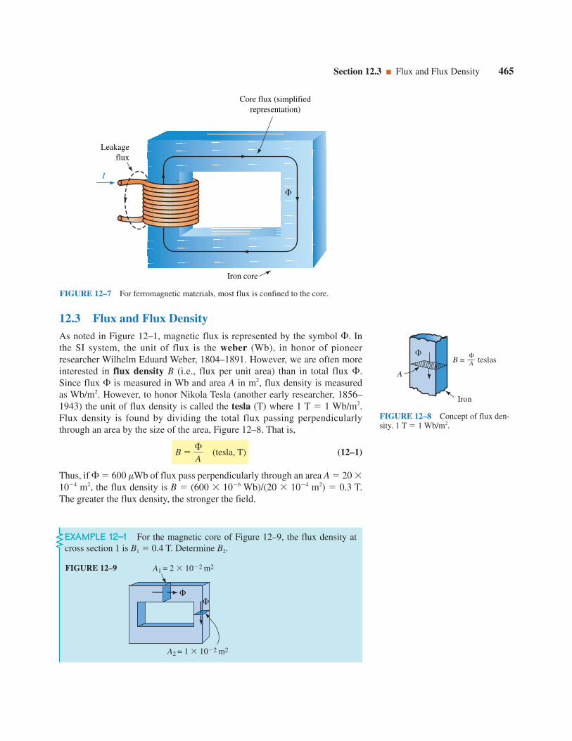
12.3 Flux and Flux DensityAs noted in Figure 12–1, magnetic flux is represented by the symbol . Inthe SI system, the unit of flux is the weber (Wb), in honor of pioneerresearcher Wilhelm Eduard Weber, 1804–1891. However, we are often moreinterested in flux density B (i.e., flux per unit area) than in total flux .Since flux is measured in Wb and area A in m2, flux density is measuredas Wb/m2. However, to honor Nikola Tesla (another early researcher, 1856–1943) the unit of flux density is called the tesla (T) where 1 T 1 Wb/m2.Flux density is found by dividing the total flux passing perpendicularlythrough an area by the size of the area, Figure 12–8. That is,
B A
(tesla, T) (12–1)
Thus, if 600 mWb of flux pass perpendicularly through an area A 20 104 m2, the flux density is B (600 106 Wb)/(20 104 m2) 0.3 T.The greater the flux density, the stronger the field.
Section 12.3 Flux and Flux Density 465
I
Leakageflux
Core flux (simplifiedrepresentation)
Iron core
B = teslas
A
Iron
A
FIGURE 12–8 Concept of flux den-sity. 1 T 1 Wb/m2.
EXAMPLE 12–1 For the magnetic core of Figure 12–9, the flux density atcross section 1 is B1 0.4 T. Determine B2.
FIGURE 12–9 A1 = 2 102 m2
A2 = 1 102 m2
FIGURE 12–7 For ferromagnetic materials, most flux is confined to the core.
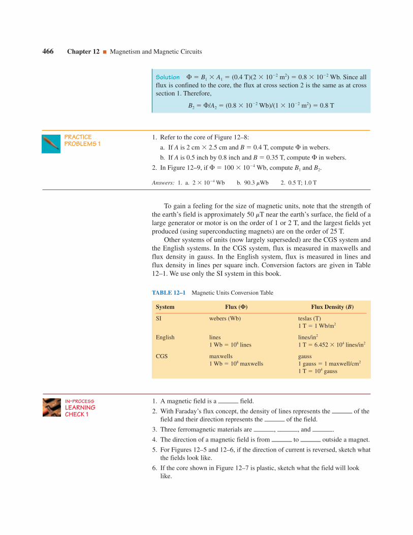
To gain a feeling for the size of magnetic units, note that the strength ofthe earth’s field is approximately 50 mT near the earth’s surface, the field of alarge generator or motor is on the order of 1 or 2 T, and the largest fields yetproduced (using superconducting magnets) are on the order of 25 T.
Other systems of units (now largely superseded) are the CGS system andthe English systems. In the CGS system, flux is measured in maxwells andflux density in gauss. In the English system, flux is measured in lines andflux density in lines per square inch. Conversion factors are given in Table12–1. We use only the SI system in this book.
466 Chapter 12 Magnetism and Magnetic Circuits
Solution B1 A1 (0.4 T)(2 102 m2) 0.8 102 Wb. Since allflux is confined to the core, the flux at cross section 2 is the same as at crosssection 1. Therefore,
B2 /A2 (0.8 102 Wb)/(1 102 m2) 0.8 T
PRACTICEPROBLEMS 1
1. Refer to the core of Figure 12–8:
a. If A is 2 cm 2.5 cm and B 0.4 T, compute in webers.
b. If A is 0.5 inch by 0.8 inch and B 0.35 T, compute in webers.
2. In Figure 12–9, if 100 104 Wb, compute B1 and B2.
Answers: 1. a. 2 104 Wb b. 90.3 mWb 2. 0.5 T; 1.0 T
TABLE 12–1 Magnetic Units Conversion Table
System Flux () Flux Density (B)
SI webers (Wb) teslas (T)1 T 1 Wb/m2
English lines lines/in2
1 Wb 108 lines 1 T 6.452 104 lines/in2
CGS maxwells gauss1 Wb 108 maxwells 1 gauss 1 maxwell/cm2
1 T 104 gauss
1. A magnetic field is a field.
2. With Faraday’s flux concept, the density of lines represents the of thefield and their direction represents the of the field.
3. Three ferromagnetic materials are , , and .
4. The direction of a magnetic field is from to outside a magnet.
5. For Figures 12–5 and 12–6, if the direction of current is reversed, sketch whatthe fields look like.
6. If the core shown in Figure 12–7 is plastic, sketch what the field will looklike.
IN-PROCESSLEARNINGCHECK 1
7. Flux density B is defined as the ratio /A, where A is the area (parallel, per-pendicular) to .
8. For Figure 12–9, if A1 is 2 cm 2.5 cm, B1 is 0.5 T, and B2 0.25 T, what isA2?
(Answers are at the end of the chapter.)
Section 12.4 Magnetic Circuits 467
12.4 Magnetic CircuitsMost practical applications of magnetism use magnetic structures to guideand shape magnetic fields by providing a well-defined path for flux. Suchstructures are called magnetic circuits. Magnetic circuits are found inmotors, generators, computer disk drives, tape recorders, and so on. Thespeaker of Figure 12–4 illustrates the concept. It uses a powerful magnet tocreate flux and an iron circuit to guide the flux to the air gap to provide theintense field required by the voice coil. Note how effectively it does its job;almost the entire flux produced by the magnet is confined to the iron pathwith little leakage into the air.
A second example is shown in Figures 12–10 and 12–11. Tape recorders,VCRs, and computer disk drives all store information magnetically on ironoxide coated surfaces for later retrieval and use. The basic tape recorderscheme is shown symbolically in Figure 12–10. Sound picked up by amicrophone is converted to an electrical signal, amplified, and the outputapplied to the record head. The record head is a small magnetic circuit. Cur-rent from the amplifier passes through its coil, creating a magnetic field thatmagnetizes the moving tape. The magnetized patterns on the tape correspondto the original sound input.
(b) Record head
(a) Recording System
Microphone
Soundwaves
Direction of tape movement
Amplifier
I
Tape
I
Tape
FIGURE 12–10 The recording head of a tape recorder is a magnetic circuit.
During playback the magnetized tape is passed by a playback head, asshown in Figure 12–11(a). Voltages induced in the playback coil are ampli-fied and applied to a speaker. The speaker (b) utilizes a flexible cone toreproduce sound. A coil of fine wire attached at the apex of this cone isplaced in the field of the speaker air gap. Current from the amplifier passesthrough this coil, creating a varying field that interacts with the fixed field of

the speaker magnet, causing the cone to vibrate. Since these vibrations corre-spond to the magnetized patterns on the tape, the original sound is repro-duced. Computer disk drives use a similar record/playback scheme; in thiscase, binary logic patterns are stored and retrieved rather than music andvoice.
12.5 Air Gaps, Fringing, and Laminated CoresFor magnetic circuits with air gaps, fringing occurs, causing a decrease influx density in the gap as in Figure 12–12(a). For short gaps, fringing canusually be neglected. Alternatively, correction can be made by increasingeach cross-sectional dimension of the gap by the size of the gap to approxi-mate the decrease in flux density.
468 Chapter 12 Magnetism and Magnetic Circuits
(b) Speaker
(a) Playback System
Amplifier
Tape
Direction of tape movement
Speaker
N
S
S
Frame mount
Permanentmagnet
Coilvibrates
Voicecoil
Soundwaves
Vibratingcone
FIGURE 12–11 Both the playback system and the speaker use magnetic circuits.
(a) Fringing at gap
(b) Laminated section. Effective magnetic area isless than the physical area
A
Φ
FIGURE 12–12 Fringing and lami-nations.

Now consider laminations. Many practical magnetic circuits (such astransformers) use thin sheets of stacked iron or steel as in Figure 12–12(b).Since the core is not a solid block, its effective cross-sectional area (i.e., theactual area of iron) is less than its physical area. A stacking factor, definedas the ratio of the actual area of ferrous material to the physical area of thecore, permits you to determine the core’s effective area.
Section 12.6 Series Elements and Parallel Elements 469
EXAMPLE 12–2 A core with cross-sectional dimensions of 2.5 cm by 3 cmhas a 0.1-mm gap. If flux density B 0.86 T in the iron, what is the approxi-mate (corrected) flux density in the gap?
Solution BA (0.86 T)(2.5 102 m)(3 102 m) 0.645 mWb
Ag (2.51 102 m)(3.01 102 m) 7.555 104 m2
Thus, in the gap
Bg 0.645 mWb/7.555 104 m2 0.854 T
PRACTICEPROBLEMS 2
A laminated section of core has cross-sectional dimensions of 0.03 m by 0.05 mand a stacking factor of 0.9.
a. What is the effective area of the core?
b. Given 1.4 103 Wb, what is the flux density, B?
Answers: a. 1.35 103 m2 b. 1.04 T
12.6 Series Elements and Parallel ElementsMagnetic circuits may have sections of different materials. For example, thecircuit of Figure 12–13 has sections of cast iron, sheet steel, and an air gap.For this circuit, flux is the same in all sections. Such a circuit is called aseries magnetic circuit. Although the flux is the same in all sections, theflux density in each section may vary, depending on its effective cross-sec-tional area as you saw earlier.
I
N turns
Cast iron
Laminatedsheetsteel
Air gap
I
1
2 3
FIGURE 12–13 Series magnetic cir-cuit. Flux is the same throughout.
FIGURE 12–14 The sum of the fluxentering a junction equals the sum leav-ing. Here, 1 2 3.

A circuit may also have elements in parallel (Figure 12–14). At eachjunction, the sum of fluxes entering is equal to the sum leaving. This isthe counterpart of Kirchhoff’s current law. Thus, for Figure 12–14, if 1 25 mWb and 2 15 mWb, then 3 10 mWb. For cores that are symmetri-cal about the center leg, 2 3.
470 Chapter 12 Magnetism and Magnetic Circuits
1. Why is the flux density in each section of Figure 12–13 different?
2. For Figure 12–13, 1.32 mWb, the cross section of the core is 3 cm by 4cm, the laminated section has a stacking factor of 0.8, and the gap is 1 mm.Determine the flux density in each section, taking fringing into account.
3. If the core of Figure 12–14 is symmetrical about its center leg, B1 0.4 T,and the cross-sectional area of the center leg is 25 cm2, what are 2 and 3?
(Answers are at the end of the chapter.)
IN-PROCESSLEARNINGCHECK 2
12.7 Magnetic Circuits with DC ExcitationWe now look at the analysis of magnetic circuits with dc excitation. Thereare two basic problems to consider: (1) given the flux, to determine the cur-rent required to produce it and (2) given the current, to compute the flux pro-duced. To help visualize how to solve such problems, we first establish ananalogy between magnetic circuits and electric circuits.
MMF: The Source of Magnetic FluxCurrent through a coil creates magnetic flux. The greater the current or thegreater the number of turns, the greater will be the flux. This flux-producingability of a coil is called its magnetomotive force (mmf). Magnetomotiveforce is given the symbol and is defined as
NI (ampere-turns, At) (12–2)
Thus, a coil with 100 turns and 2.5 amps will have an mmf of 250 ampere-turns, while a coil with 500 turns and 4 amps will have an mmf of 2000ampere-turns.
Reluctance, : Opposition to Magnetic FluxFlux in a magnetic circuit also depends on the opposition that the circuit pre-sents to it. Termed reluctance, this opposition depends on the dimensions ofthe core and the material of which it is made. Like the resistance of a wire,reluctance is directly proportional to length and inversely proportional tocross-sectional area. In equation form,
m
A (At/Wb) (12–3)
where m is a property of the core material called its permeability (discussedin Section 12.8). Permeability is a measure of how easy it is to establish fluxin a material. Ferromagnetic materials have high permeability and hence low, while nonmagnetic materials have low permeability and high .

Ohm’s Law for Magnetic CircuitsThe relationship between flux, mmf, and reluctance is
/ (Wb) (12–4)
This relationship is similar to Ohm’s law and is depicted symbolically inFigure 12–15. (Remember however that flux, unlike electric current, doesnot flow—see note in Section 12.1.)
Section 12.8 Magnetic Field Intensity and Magnetization Curves 471
FIGURE 12–15 Electric circuit anal-ogy of a magnetic circuit. /.
EXAMPLE 12–3 For Figure 12–16, if the reluctance of the magnetic circuitis 12 104 At/Wb, what is the flux in the circuit?
Solution NI (300)(0.5 A) 150 At
/ (150 At)/(12 104 At/Wb) 12.5 104 Wb
FIGURE 12–160.5 A
N = 300 turns
In Example 12–3, we assumed that the reluctance of the core was con-stant. This is only approximately true under certain conditions. In general, it isnot true, since is a function of flux density. Thus Equation 12–4 is not reallyvery useful, since for ferromagnetic material, depends on flux, the veryquantity that you are trying to find. The main use of Equations 12–3 and 12–4is to provide an analogy between electric and magnetic circuit analysis.
12.8 Magnetic Field Intensity and Magnetization CurvesWe now look at a more practical approach to analyzing magnetic circuits.First, we require a quantity called magnetic field intensity, H (also known asmagnetizing force). It is a measure of the mmf per unit length of a circuit.
To get at the idea, suppose you apply the same mmf (say 600 At) to twocircuits with different path lengths (Figure 12–17). In (a), you have 600ampere-turns of mmf to “drive” flux through 0.6 m of core; in (b), you havethe same mmf but it is spread across only 0.15 m of path length. Thus themmf per unit length in the second case is more intense. Based on this idea,one can define magnetic field intensity as the ratio of applied mmf to thelength of path that it acts over. Thus,
H / NI/ (At/m) (12–5)
For the circuit of Figure 12–17(a), H 600 At/0.6 m 1000 At/m, whilefor the circuit of (b), H 600 At/0.15 4000 At/m. Thus, in (a) you have
(a) A long path
(b) A short path
CoilI
mmf = NI
I
l = 0.15 m
mmf = NI
l = 0.6 m
FIGURE 12–17 By definition, H mmf/length NI/.

1000 ampere-turns of “driving force” per meter of length to establish flux inthe core, whereas in (b) you have four times as much. (However, you won’tget four times as much flux, since the opposition to flux varies with the den-sity of the flux.)
Rearranging Equation 12–5 yields an important result:
NI H (At) (12–6)
In an analogy with electric circuits (Figure 12–18), the NI product is an mmfsource, while the H product is an mmf drop.
The Relationship between B and HFrom Equation 12–5, you can see that magnetizing force, H, is a measure ofthe flux-producing ability of the coil (since it depends on NI). You also knowthat B is a measure of the resulting flux (since B /A). Thus, B and H arerelated. The relationship is
B mH (12–7)
where m is the permeability of the core (recall Equation 12–3).It was stated earlier that permeability is a measure of how easy it is to
establish flux in a material. To see why, note from Equation 12–7 that thelarger the value of m, the larger the flux density for a given H. However, H isproportional to current; therefore, the larger the value of m, the larger theflux density for a given magnetizing current. From this, it follows that thelarger the permeability, the more flux you get for a given magnetizing cur-rent.
In the SI system, m has units of webers per ampere-turn-meter. The per-meability of free space is m0 4p 107. For all practical purposes, thepermeability of air and other nonmagnetic materials is the same as for a vac-uum. Thus, in air gaps,
Bg m0Hg 4p 107 Hg (12–8)
Rearranging Equation 12–8 yields
Hg 4p
Bg
107 7.96 105Bg (At/m) (12–9)
472 Chapter 12 Magnetism and Magnetic Circuits
NI Hl
NI = Hl
FIGURE 12–18 Circuit analogy, Hmodel.
PRACTICEPROBLEMS 3
For Figure 12–16, the core cross section is 0.05 m 0.08 m. If a gap is cut inthe core and H in the gap is 3.6 105 At/m, what is the flux in the core?Neglect fringing.
Answer: 1.81 mWb
B-H CurvesFor ferromagnetic materials, m is not constant but varies with flux densityand there is no easy way to compute it. In reality, however, it isn’t m that youare interested in: What you really want to know is, given B, what is H, andvice versa. A set of curves, called B-H or magnetization curves, provides thisinformation. (These curves are obtained experimentally and are available in

handbooks. A separate curve is required for each material.) Figure 12–19shows typical curves for cast iron, cast steel, and sheet steel.
Section 12.8 Magnetic Field Intensity and Magnetization Curves 473
1.6
1.4
1.2
1.0
0.8
0.6
0.4
0.2
0
0 500 1000 1500 2000 2500 3000 3500 4000 4500 5000
B (T)
H (At/m)
Sheet steel
Cast steel
Cast iron
FIGURE 12–19 B-H curves for selected materials.
EXAMPLE 12–4 If B 1.4 T for sheet steel, what is H?
Solution Enter Figure 12–19 on the axis at B 1.4 T, continue across untilyou encounter the curve for sheet steel, then read the corresponding value forH as indicated in Figure 12–20: H 1000 At/m.
1.4
1000
Sheet steel
B (T)
H (At/m)
FIGURE 12–20 For sheet steel, H 1000 At/m when B 1.4 T.

12.9 Ampere’s Circuital LawOne of the key relationships in magnetic circuit theory is Ampere’s cir-cuital law. Ampere’s law was determined experimentally and is a generaliza-tion of the relationship NI H that we developed earlier. Ampereshowed that the algebraic sum of mmfs around a closed loop in a magneticcircuit is zero, regardless of the number of sections or coils. That is,
0 (12–10)
This can be rewrittten as
NI H At (12–11)
which states that the sum of applied mmfs around a closed loop equals thesum of the mmf drops. The summation is algebraic and terms are additive orsubtractive, depending on the direction of flux and how the coils are wound.To illustrate, consider again Figure 12–13. Here,
NI Hironiron Hsteelsteel Hgg 0
Thus,
NI Hironiron Hsteelsteel Hgg
Impressed sum of mmf dropsmmf
which states that the applied mmf NI is equal to the sum of the H dropsaround the loop. The path to use for the H terms is the mean (average) path.
You now have two magnetic circuit models (Figure 12–21). While thereluctance model (a) is not very useful for solving problems, it helps relatemagnetic circuit problems to familiar electrical circuit concepts. TheAmpere’s law model, on the other hand, permits us to solve practical prob-lems. We look at how to do this in the next section.
474 Chapter 12 Magnetism and Magnetic Circuits
PRACTICEPROBLEMS 4
The cross section of a sheet steel core is 0.1 m 0.1 m and its stacking factor is0.93. If H 1500 At/m, compute flux density B and magnetic flux .
Answer: 1.45 T 13.5 mWb
(a) Reluctance model
iron
steel
g
(b) Ampere’s circuital law model
Hiron liron
Hsteel lsteel
Hg lg
FIGURE 12–21 Two models for the magnetic circuit of Figure 12–13.
6. For the circuit of Figure 12–23, the length to use in Ampere’s law is (0.36m, 0.32 m, 0.28 m). Why?
(Answers are at the end of the chapter.)
Section 12.10 Series Magnetic Circuits: Given , Find NI 475
IN-PROCESSLEARNINGCHECK 3
1. If the mmf of a 200-turn coil is 700 At, the current in the coil is amps.
2. For Figure 12–17, if H 3500 At/m and N 1000 turns, then for (a), I is A, while for (b), I is A.
3. For cast iron, if B 0.5 T, then H At/m.
4. A circuit consists of one coil, a section of iron, a section of steel, and two airgaps (of different sizes). Draw the Ampere’s law model.
5. Which is the correct answer for the circuit of Figure 12–22?
a. Ampere’s law around loop 1 yields (NI H11 H22, or NI H11 H22).
b. Ampere’s law around loop 2 yields (0 H22 H33, or 0 H22 H33).
Path l1 = labcH = H1
Path l3 = lcdaH = H3
Path l2 = lcaH = H2
a
b
c
d
1 cm 1 cm
1 cm
1 cm
6 cm
8 cm
FIGURE 12–22 FIGURE 12–23
12.10 Series Magnetic Circuits: Given , Find NIYou now have the tools needed to solve basic magnetic circuit problems. Wewill begin with series circuits where is known and we want to find theexcitation to produce it. Problems of this type can be solved using four basicsteps:
1. Compute B for each section using B /A.
2. Determine H for each magnetic section from the B-H curves. Use Hg 7.96 105Bg for air gaps.
3. Compute NI using Ampere’s circuital law.
4. Use the computed NI to determine coil current or turns as required. (Cir-cuits with more than one coil are handled as in Example 12–6.)
Be sure to use the mean path through the circuit when applying Ampere’slaw. Unless directed otherwise, neglect fringing.

476 Chapter 12 Magnetism and Magnetic Circuits
PRACTICAL NOTES...Magnetic circuit analysis is not as precise as electric circuit analysis because(1) the assumption of uniform flux density breaks down at sharp corners asyou saw in Figure 12–4, and (2) the B-H curve is a mean curve and has con-siderable uncertainty as discussed later (Section 12–14).
Although the answers are approximate, they are adequate for most pur-poses.
EXAMPLE 12–5 If the core of Figure 12–24 is cast iron and 0.1 103 Wb, what is the coil current?
Solution Following the four steps outlined above:
1. The flux density is
B A
00..12
1100
3
3 0.5 T
2. From the B-H curve (cast iron), Figure 12–19, H 1550 At/m.
3. Apply Ampere’s law. There is only one coil and one core section. Length 0.25 m. Thus,
NI H 1550 0.25 388 At
4. Divide by N:
I 388/500 0.78 amps
Mean length abcda = 0.25 m
Area A B = A
N = 500 turnsA = 0.2 103 m2
I
a b
cd
FIGURE 12–24

Note. Since magnetic circuits are nonlinear, you cannot use superposition,that is, you cannot consider each coil of Figure 12–25 by itself, then sum theresults. You must consider them simultaneously as we did in Example 12–6.
More ExamplesIf a magnetic circuit contains an air gap, add another element to the concep-tual models (recall Figure 12–21). Since air represents a poor magnetic path,its reluctance will be high compared with that of iron. Recalling our analogyto electric circuits, this suggests that the mmf drop across the gap will be largecompared with that of the iron. You can see this in the following example.
Section 12.10 Series Magnetic Circuits: Given , Find NI 477
EXAMPLE 12–6 A second coil is added as shown in Figure 12–25. If 0.1 103 Wb as before, but I1 1.5 amps, what is I2?
I1 I2
N1 = 500 N2 = 200
FIGURE 12–25
Solution From the previous example, you know that a current of 0.78 ampsin coil 1 produces 0.1 103 Wb. But you already have 1.5 amps in coil1. Thus, coil 2 must be wound in opposition so that its mmf is subtractive.Applying Ampere’s law yields N1I1 N2I2 H. Hence,
(500)(1.5 A) 200I2 388 At
and so I2 1.8 amps.
EXAMPLE 12–7 The core of Figure 12–24 has a 0.008-m gap cut as shownin Figure 12–26. Determine how much the current must increase to maintainthe original core flux. Neglect fringing.
(a)
I
lg = 0.008 m
(b)
NI
Hiron liron
Hg lg
FIGURE 12–26

478 Chapter 12 Magnetism and Magnetic Circuits
SolutionIroniron 0.25 0.008 0.242 m. Since does not change, B and H will bethe same as before. Thus, Biron 0.5 T and Hiron 1550 At/m.
Air GapBg is the same as Biron. Thus, Bg 0.5 T and Hg 7.96 105Bg 3.98 105
At/m.
Ampere’s LawNI Hironiron Hgg (1550)(0.242) (3.98 105)(0.008) 375 3184 3559 At. Thus, I 3559/500 7.1 amps. Note that the current had toincrease from 0.78 amp to 7.1 amps in order to maintain the same flux, over aninefold increase.
EXAMPLE 12–8 The laminated sheet steel section of Figure 12–27 has astacking factor of 0.9. Compute the current required to establish a flux of 1.4 104 Wb. Neglect fringing.
I
N = 150
Cast iron
Laminatedsheet steel(SF = 0.9)
e
d c b
fg
ha
lg = 0.2"0.5"
0.8"
lef = 2.5"lde = 2"
Cross section = 0.5" 0.8" (all members) = 1.4 104 Wb
FIGURE 12–27
Solution Convert all dimensions to metric.
Cast Iron
iron ab cdef 2.5 2 2.5 0.2 6.8 in 0.173 m
Airon (0.5 in)(0.8 in) 0.4 in2 0.258 103 m2
Biron /Airon (1.4 104)/(0.258 103) 0.54 T
Hiron 1850 At/m (from Figure 12–19)
Sheet Steel
steel fg gh ha 0.25 2 0.25 2.5 in 6.35 102 m
Asteel (0.9)(0.258 103) 0.232 103 m2
Bsteel /Asteel (1.4 104)/(0.232 103) 0.60 T
Hsteel 125 At/m (from Figure 12–19)

Section 12.10 Series Magnetic Circuits: Given , Find NI 479
Air Gap
g 0.2 in 5.08 103 m
Bg Biron 0.54 T
Hg (7.96 105)(0.54) 4.3 105 At/m
Ampere’s Law
NI Hironiron Hsteelsteel Hgg
(1850)(0.173) (125)(6.35 102) (4.3 105)(5.08 103)
320 7.9 2184 2512 At
I 2512/N 2512/150 16.7 amps
EXAMPLE 12–9 Figure 12–28 shows a portion of a solenoid. Flux 4 104 Wb when I 2.5 amps. Find the number of turns on the coil.
I
lg
Gap
Spring
Plunger
0.4 cm
Yoke
Coil
2 cm
2.5 cm
l plunger = 0.1 m
Cross section2.5 cm 2.5 cm
lyoke = 0.2 m
FIGURE 12–28 Solenoid. All parts are cast steel.
SolutionYoke
Ayoke 2.5 cm 2.5 cm 6.25 cm2 6.25 104 m2
Byoke A
yoke
6.
425
101
0
4
4 0.64 T
Hyoke 410 At/m (from Figure 12–19)
Plunger
Aplunger 2.0 cm 2.5 cm 5.0 cm2 5.0 104 m2
Bplunger Ap
lunger
54.0
1100
4
4 0.8 T
Hplunger 500 At/m (from Figure 12–19)
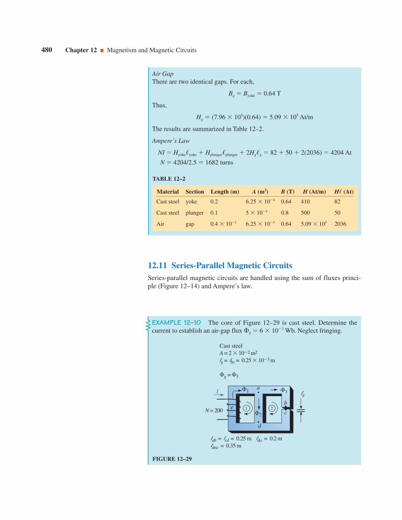
12.11 Series-Parallel Magnetic CircuitsSeries-parallel magnetic circuits are handled using the sum of fluxes princi-ple (Figure 12–14) and Ampere’s law.
480 Chapter 12 Magnetism and Magnetic Circuits
Air GapThere are two identical gaps. For each,
Bg Byoke 0.64 T
Thus,
Hg (7.96 105)(0.64) 5.09 105 At/m
The results are summarized in Table 12–2.
Ampere’s Law
NI Hyokeyoke Hplungerplunger 2Hgg 82 50 2(2036) 4204 At
N 4204/2.5 1682 turns
TABLE 12–2
Material Section Length (m) A (m2) B (T) H (At/m) H (At)
Cast steel yoke 0.2 6.25 104 0.64 410 82
Cast steel plunger 0.1 5 104 0.8 500 50
Air gap 0.4 102 6.25 104 0.64 5.09 105 2036
EXAMPLE 12–10 The core of Figure 12–29 is cast steel. Determine thecurrent to establish an air-gap flux g 6 103 Wb. Neglect fringing.
I 1 3
2
e
a
b
c
d
N = 200 1 2
lab = lcd = 0.25 m lda = 0.2 mldea = 0.35 m
Cast steelA = 2 102 m2
lg = lbc = 0.25 103 m
g = 3
lg
FIGURE 12–29

Answer: 6.5 A
Section 12.11 Series-Parallel Magnetic Circuits 481
Solution Consider each section in turn.
Air Gap
Bg g/Ag (6 103)/(2 102) 0.3 T
Hg (7.96 105)(0.3) 2.388 105 At/m
Sections ab and cd
Bab Bcd Bg 0.3 T
Hab Hcd 250 At/m (from Figure 12–19)
Ampere’s Law (Loop 2)
NI H. Since you are going opposite to flux in leg da, the corre-
sponding term (i.e., Hdada) will be subtractive. Also, NI 0 for loop 2. Thus,
0 loop2 H
0 Habab Hgg Hcdcd Hdada
(250)(0.25) (2.388 105)(0.25 103) (250)(0.25) 0.2Hda
62.5 59.7 62.5 0.2Hda 184.7 0.2Hda
Thus, 0.2Hda 184.7 and Hda 925 At/m. From Figure 12–19, Bda 1.12 T.
2 BdaA 1.12 0.02 2.24 102 Wb
1 2 3 2.84 102 Wb.
Bdea 1/A (2.84 102)/0.02 1.42 T
Hdea 2125 At/m (from Figure 12–19)
Ampere’s Law (Loop 1)
NI Hdeadea Hadad (2125)(0.35) 184.7 929 At
I 929/200 4.65 A
PRACTICEPROBLEMS 5
The cast-iron core of Figure 12–30 is symmetrical. Determine current I. Hint: Tofind NI, you can write Ampere’s law around either loop. Be sure to make use ofsymmetry.
FIGURE 12–30
I
1
a b c
d
2
lab = lbc = lcd = 4 cmGap: lg = 0.5 cmlek = 3 cm
Core dimensions: 1 cm 1 cm
k
2 = 30 Wb
N = 400
1 2
ef
m

12.12 Series Magnetic Circuits: Given NI, Find In previous problems, you were given the flux and asked to find the current.We now look at the converse problem: given NI, find the resultant flux. Forthe special case of a core of one material and constant cross section (Exam-ple 12–11) this is straightforward. For all other cases, trial and error must beused.
482 Chapter 12 Magnetism and Magnetic Circuits
EXAMPLE 12–11 For the circuit of Figure 12–31, NI 250 At. Deter-mine .
Solution H NI. Thus, H NI/ 250/0.2 1250 At/m. From the B-Hcurve of Figure 12–19, B 1.24 T. Therefore, BA 1.24 0.01 1.24 102 Wb.
FIGURE 12–31
I
Cast steelN turns
l = 0.2 m
Cross-sectionalarea A = 0.01 m2
For circuits with two or more sections, the process is not so simple.Before you can find H in any section, for example, you need to know theflux density. However, in order to determine flux density, you need to knowH. Thus, neither nor H can be found without knowing the other first.
To get around this problem, use trial and error. First, take a guess at thevalue for flux, compute NI using the 4-step procedure of Section 12.10, thencompare the computed NI against the given NI. If they agree, the problem issolved. If they don’t, adjust your guess and try again. Repeat the procedureuntil you are within 5% of the given NI.
The problem is how to come up with a good first guess. For circuits ofthe type of Figure 12–32, note that NI Hsteelsteel Hgg. As a first guess,assume that the reluctance of the air gap is so high that the full mmf dropappears across the gap. Thus, NI Hgg, and
Hg NI/g (12–12)
You can now apply Ampere’s law to see how close to the given NI your trialguess is.
Since we know that some of the mmf drop appears across the steel, wewill start at less than 100% for the gap. Common sense and a bit of experi-ence helps. The relative size of the mmf drops also depends on the corematerial. For cast iron, the percentage drop across the iron is larger than the
I
lg
= Hsteel lsteel Hg lg
Hg lg if Hg lg >> Hsteel lsteel
lg = 0.002 mlsteel = 0.2 m
FIGURE 12–32

percentage across a similar piece of sheet steel or cast steel. This is illus-trated in the next two examples.
Section 12.12 Series Magnetic Circuits: Given NI, Find 483
EXAMPLE 12–12 The core of Figure 12–32 is cast steel, NI 1100 At,and the cross-sectional area everywhere is 0.0025 m2. Determine the flux inthe core.
SolutionInitial GuessAssume that 90% of the mmf appears across the gap. The applied mmf is1100 At. Ninety percent of this is 990 At. Thus, Hg 0.9NI/ 990/0.002 4.95 105 At/m and Bg m0Hg (4p 107)(4.95 105) 0.62 T.
Trial 1Since the area of the steel is the same as that of the gap, the flux density is thesame, neglecting fringing. Thus, Bsteel Bg 0.62 T. From the B-H curve,Hsteel 400 At/m. Now apply Ampere’s law:
NI Hsteelsteel Hgg (400)(0.2) (4.95 105)(0.002) 80 990 1070 At
This answer is 2.7% lower than the given NI of 1100 At and is thereforeacceptable. Thus, BA 0.62 0.0025 1.55 103 Wb.
The initial guess in Example 12–12 yielded an acceptable answer on thefirst trial. (You are seldom this lucky.)
EXAMPLE 12–13 If the core of Figure 12–32 is cast iron instead of steel,compute .
Solution Because cast iron has a larger H for a given flux density (Figure12–19), it will have a larger H drop and less will appear across the gap.Assume 75% across the gap.
Initial GuessHg 0.75 NI/ (0.75)(1100)/0.002 4.125 105 At/m.
Bg m0Hg (4m 107)(4.125 105) 0.52 T.
Trial 1Biron Bg. Thus, Biron 0.52 T. From the B-H curve, Hiron 1700 At/m.
Ampere’s Law
NI Hironiron Hgg (1700)(0.2) (4.125 105)(0.002) 340 825 1165 At (high by 5.9%)
Trial 2Reduce the guess by 5.9% to Biron 0.49 T. Thus, Hiron 1500 At/m (fromthe B-H curve) and Hg 7.96 105 Bg 3.90 105 At/m.

12.13 Force Due to an ElectromagnetElectromagnets are used in relays, door bells, lifting magnets, and so on. Foran electromagnetic relay as in Figure 12–33, it can be shown that the forcecreated by the magnetic field is
F B
2
2g
m
A
0
g (12–13)
where Bg is flux density in the gap in teslas, Ag is gap area in square meters,and F is force in newtons.
484 Chapter 12 Magnetism and Magnetic Circuits
Ampere’s Law
NI Hironiron Hgg (1500)(0.2) (3.90 105)(0.002) 300 780 1080 At
The error is now 1.82%, which is excellent. Thus, BA (0.49)(2.5 103) 1.23 103 Wb. If the error had been larger than 5%, a new trialwould have been needed.
EXAMPLE 12–14 Figure 12–33 shows a typical relay. The force due to thecurrent-carrying coil pulls the pivoted arm against spring tension to close thecontacts and energize the load. If the pole face is 1⁄4 inch square and 0.5 104 Wb, what is the pull on the armature in pounds?
Contacts
Coil
FIGURE 12–33 A typical relay.
Solution Convert to metric units.
Ag (0.25 in)(0.25 in) 0.0625 in2 0.403 104 m2
Bg /Ag (0.5 104)/(0.403 104) 1.24 T

Figure 12–34 shows how a relay is used in practice. When the switch isclosed, the energized coil pulls the armature down. This closes the contactsand energizes the load. When the switch is opened, the spring pulls the con-tacts open again. Schemes like this use relatively small currents to controllarge loads. In addition, they permit remote control, as the relay and loadmay be a considerable distance from the actuating switch.
Section 12.14 Properties of Magnetic Materials 485
Thus,
F B
2
2g
m
A
0
24.66 N 5.54 lb(1.24)2(0.403 104)
2(4p 107)
I
Contacts
Spring
Pivot pointInsulationArmature
Coil
ELoad
FIGURE 12–34 Controlling a load with a relay.
12.14 Properties of Magnetic MaterialsMagnetic properties are related to atomic structure. Each atom of a sub-stance, for example, produces a tiny atomic-level magnetic field because itsmoving (i.e., orbiting) electrons constitute an atomic-level current and cur-rents create magnetic fields. For nonmagnetic materials, these fields arerandomly oriented and cancel. However, for ferromagnetic materials, thefields in small regions, called domains (Figure 12–35), do not cancel.(Domains are of microscopic size, but are large enough to hold from 1017
to 1021 atoms.) If the domain fields in a ferromagnetic material line up, thematerial is magnetized; if they are randomly oriented, the material is notmagnetized.
Magnetizing a SpecimenA nonmagnetized specimen can be magnetized by making its domain fieldsline up. Figure 12–36 shows how this can be done. As current through thecoil is increased, the field strength increases and more and more domains
Ferromagneticmaterial
FIGURE 12–35 Random orientationof microscopic fields in a nonmagne-tized ferromagnetic material. The smallregions are called domains.

align themselves in the direction of the field. If the field is made strongenough, almost all domain fields line up and the material is said to be in sat-uration (the almost flat portion of the B-H curve). In saturation, the fluxdensity increases slowly as magnetization intensity increases. This meansthat once the material is in saturation, you cannot magnetize it much furtherno matter how hard you try. Path 0-a traced from the nonmagnetized state tothe saturated state is termed the dc curve or normal magnetization curve.(This is the B-H curve that you used earlier when you solved magnetic cir-cuit problems.)
486 Chapter 12 Magnetism and Magnetic Circuits
(a) The magnetizingcircuit
FerromagneticmaterialE
I
(b) Progressive change in thedomain orientations as the
field is increased. H is proportional to current I
B
0
a
Saturation
H
FIGURE 12–36 The magnetization process.
HysteresisIf you now reduce the current to zero, you will find that the material stillretains some magnetism, called residual magnetism (Figure 12–37, pointb). If now you reverse the current, the flux reverses and the bottom part ofthe curve can be traced. By reversing the current again at d, the curve can betraced back to point a. The result is called a hysteresis loop. A major sourceof uncertainty in magnetic circuit behavior should now be apparent: As youcan see, flux density depends not just on current, it also depends on whicharm of the curve the sample is magnetized on, i.e., it depends on the circuit’spast history. For this reason, B-H curves are the average of the two arms ofthe hysteresis loop, i.e., the dc curve of Figure 12–36.
The Demagnetization ProcessAs indicated above, simply turning the current off does not demagnetize fer-romagnetic material. To demagnetize it, you must successively decrease itshysteresis loop to zero as in Figure 12–38. You can place the specimen insidea coil that is driven by a variable ac source and gradually decrease the coilcurrent to zero, or you can use a fixed ac supply and gradually withdraw thespecimen from the field. Such procedures are used by service personnel to“degauss” TV picture tubes.
B
H
a
c
b
d
Residualmagnetism
Residualmagnetism
FIGURE 12–37 Hysteresis loop.
B
H
FIGURE 12–38 Demagnetization bysuccessively shrinking the hysteresisloop.

12.15 Measuring Magnetic FieldsOne way to measure magnetic field strength is to use the Hall effect (after E.H. Hall). The basic idea is illustrated in Figure 12–39. When a strip of semi-conductor material such as indium arsenide is placed in a magnetic field, asmall voltage, called the Hall voltage, VH, appears across opposite edges. Fora fixed current I, VH is proportional to magnetic field strength B. Instrumentsusing this principle are known as Hall-effect gaussmeters. To measure amagnetic field with such a meter, insert its probe into the field perpendicularto the field (Figure 12–40). The meter indicates flux density directly.
Problems 487
I
Current source
VH
Flux
I
Hall effectprobe
Gaussmeter
4 7 3
FIGURE 12–39 The Hall effect.
FIGURE 12–40 Magnetic field measurement.
PROBLEMS12.3 Flux and Flux Density
1. Refer to Figure 12–41:
a. Which area, A1 or A2, do you use to calculate flux density?
b. If 28 mWb, what is flux density in teslas?
2. For Figure 12–41, if 250 mWb, A1 1.25 in2, and A2 2.0 in2, what isthe flux density in the English system of units?
3. The toroid of Figure 12–42 has a circular cross section and 628 mWb.If r1 8 cm and r2 12 cm, what is the flux density in teslas?
4. If r1 of Figure 12–42 is 3.5 inches and r2 is 4.5 inches, what is the flux den-sity in the English system of units if 628 mWb?

12.5 Air Gaps, Fringing, and Laminated Cores
5. If the section of core in Figure 12–43 is 0.025 m by 0.04 m, has a stackingfactor of 0.85, and B 1.45 T, what is in webers?
6. If the core of Figure 12–43 is 3 cm by 2 cm, has a stacking factor of 0.9,and B 8 103 gauss, what is in maxwells?
12.6 Series Elements and Parallel Elements
7. For the iron core of Figure 12–44, flux density B2 0.6 T. Compute B1 andB3.
488 Chapter 12 Magnetism and Magnetic Circuits
A1
0.02 m2 0.024 m2
A2
Portion ofmagnetic
circuit(cast steel)
I
r1
r2
FIGURE 12–41 FIGURE 12–42
FIGURE 12–43
A1 = 0.02 m2
A3 = 0.01 m2 A2 = 0.015 m2
B2 = 0.6 T
I
A1 = 0.02 m2
A2 = 0.01 m2
A3 = 0.016 m22
13
FIGURE 12–44 FIGURE 12–45
8. For the section of iron core of Figure 12–45, if 1 12 mWb and 3 2 mWb, what is B2?
9. For the section of iron core of Figure 12–45, if B1 0.8 T and B2 0.6 T,what is B3?
12.8 Magnetic Field Intensity and Magnetization Curves
10. Consider again Figure 12–42. If I 10 A, N 40 turns, r1 5 cm, andr2 7 cm, what is H in ampere-turns per meter?
11. Figure 12–46 shows the two electric circuit equivalents for magnetic cir-cuits. Show that m in /mA is the same as m in B mH.
12.9 Ampere’s Circuital Law
12. Let H1 and 1 be the magnetizing force and path length respectively, whereflux 1 exists in Figure 12–47 and similarly for 2 and 3. Write Ampere’slaw around each of the windows.
(b) B = H
Hl
(a) = l A
FIGURE 12–46 NI.

13. Assume that a coil N2 carrying current I2 is added on leg 3 of the core shownin Figure 12–47 and that it produces flux directed upward. Assume, how-ever, that the net flux in leg 3 is still downward. Write the Ampere’s lawequations for this case.
14. Repeat Problem 13 if the net flux in leg 3 is upward but the directions of 1
and 2 remain as in Figure 12–47.
12.10 Series Magnetic Circuits: Given , Find NI
15. Find the current I in Figure 12–48 if 0.16 mWb.
16. Let everything be the same as in Problem 15 except that the cast steel por-tion is replaced with laminated sheet steel with a stacking factor of 0.85.
17. A gap of 0.5 mm is cut in the cast steel portion of the core in Figure 12–48.Find the current for 0.128 mWb. Neglect fringing.
18. Two gaps, each 1 mm, are cut in the circuit of Figure 12–48, one in the caststeel portion and the other in the cast iron portion. Determine current for 0.128 mWb. Neglect fringing.
19. The cast iron core of Figure 12–49 measures 1 cm 1.5 cm, g 0.3 mm,the air gap flux density is 0.426 T and N 600 turns. The end pieces arehalf circles. Taking into account fringing, find current I.
Problems 489
I1
N1
H1 and l1this path
H3 and l3this path
H2 and l2this path
1
2 3
FIGURE 12–47
l steel =0.14 m
l iron =0.06 m
Castiron
Cast steel
I
A = 3.2 104 m2
N = 300 turns
FIGURE 12–48
I
N
1.5 cm
1 cm
3.2 cmlg
FIGURE 12–49
20. For the circuit of Figure 12–50, 141 mWb and N 400 turns. The bot-tom member is sheet steel with a stacking factor of 0.94, while the remain-der is cast steel. All pieces are 1 cm 1 cm. The length of the cast steelpath is 16 cm. Find current I.
21. For the circuit of Figure 12–51, 30 mWb and N 2000 turns. Neglect-ing fringing, find current I.
22. For the circuit of Figure 12–52, 25,000 lines. The stacking factor forthe sheet steel portion is 0.95. Find current I.
23. A second coil of 450 turns with I2 4 amps is wound on the cast steel por-tion of Figure 12–52. Its flux is in opposition to the flux produced by the

original coil. The resulting flux is 35 000 lines in the counterclockwisedirection. Find the current I1.
12.11 Series-Parallel Magnetic Circuits
24. For Figure 12–53, if g 80 mWb, find I.
25. If the circuit of Figure 12–53 has no gap and 3 0.2 mWb, find I.
12.12 Series Magnetic Circuits: Given NI, Find
26. A cast steel magnetic circuit with N 2500 turns, I 200 mA, and a cross-sectional area of 0.02 m2 has an air gap of 0.00254 m. Assuming 90% of themmf appears across the gap, estimate the flux in the core.
27. If NI 644 At for the cast steel core of Figure 12–54, find the flux, .
28. A gap 0.004 m is cut in the core of Figure 12–54. Everything elseremains the same. Find the flux, .
490 Chapter 12 Magnetism and Magnetic Circuits
I
N
10 cm
Sheet steel
FIGURE 12–50
ICast iron
Cast steel
lg = 2 mm
l iron = 3 cml steel = 8 cm
A (everywhere) = 0.5 cm2
I
Area of all sections (except A1) = 2 in2
N = 600
Sheetsteel
Cast steel
l1 = 2 in A1 = 1 in2
l4 l3
l2
l1 Cast iron
l2 = 3.5 in
lg = 0.2 in
l3 = 5.8 in
l4 = 7.5 in
FIGURE 12–51 FIGURE 12–52
I1 a 3
b
c
d
2
lg = lxy = 0.001 m
labc = 0.14 m
lcda = 0.16 m
lax = lcy = 0.039 m
A = 4 cm2 everywhere
x
y
100 turns
Cast steel
FIGURE 12–53

12.13 Force Due to an Electromagnet
29. For the relay of Figure 12–34, if the pole face is 2 cm by 2.5 cm and a forceof 2 pounds is required to close the gap, what flux (in webers) is needed?
30. For the solenoid of Figure 12–28, 4 104 Wb. Find the force ofattraction on the plunger in newtons and in pounds.
Answers to In-Process Learning Checks 491
I
Diameter = 2 cm
Cast steel
N
Radius = 6 cm
FIGURE 12–54
ANSWERS TO IN-PROCESSLEARNING CHECKS
In-Process Learning Check 1
1. Force
2. Strength, direction
3. Iron, nickel, cobalt
4. North, south
5. Same except direction of flux reversed
6. Same as Figure 12–6
7. Perpendicular
8. 10 cm2
In-Process Learning Check 2
1. While flux is the same throughout, the effective area of each section differs.
2. Biron 1.1 T; Bsteel 1.38 T; Bg 1.04 T
3. 2 3 0.5 mWb
In-Process Learning Check 3
1. 3.5 A
2. a. 2.1 A b. 0.525 A
3. 1550 At/m
4. Same as Figure 12–21(b) except add Hg2g2
.
5. a. NI H11 H22 b. 0 H22 H33
6. 0.32 m; use the mean path length.

OBJECTIVES
After studying this chapter, you will beable to
• describe what an inductor is and what itseffect on circuit operation is,
• explain Faraday’s law and Lenz’s law,
• compute induced voltage using Fara-day’s law,
• define inductance,
• compute voltage across an inductance,
• compute inductance for series and paral-lel configurations,
• compute inductor voltages and currentsfor steady state dc excitation,
• compute energy stored in an inductance,
• describe common inductor problems andhow to test for them.
KEY TERMS
Back Voltage
Choke
Counter EMF
Faraday’s Law
Flux Linkage
Henry
Induced Voltage
Inductance
Inductor
L
Lenz’s Law
Nf
Stray Inductance
OUTLINE
Electromagnetic Induction
Induced Voltage and Induction
Self-Inductance
Computing Induced Voltage
Inductances in Series and Parallel
Practical Considerations
Inductance and Steady State DC
Energy Stored by an Inductance
Inductor Troubleshooting Hints
Inductance and Inductors13

In this chapter, we look at self-inductance and inductors. Self-inductance (usu-ally just called inductance) is a circuit property that is due entirely to the mag-
netic field created by current in a circuit. The effect that inductance has on cir-cuit operation is to oppose any change in current—thus, in a sense, inductancecan be likened to inertia in a mechanical system.
A circuit element built to possess inductance is called an inductor. In itssimplest form an inductor is simply a coil of wire, Figure 13–1(a). Ideally,inductors have only inductance. However, since they are made of wire, practicalinductors also have some resistance. Initially, however, we assume that this resis-tance is negligible and treat inductors as ideal (i.e., we assume that they have noproperty other than inductance). (Coil resistance is considered in Sections 13.6and 13.7.) In practice, inductors are also referred to as chokes (because they tryto limit or “choke” current change), or as reactors (for reasons to be discussed inChapter 16). In this chapter, we refer to them mainly as inductors.
493
CHAPTER PREVIEW
FIGURE 13–1 Inductance is due to the magnetic field created by an electric current.
On circuit diagrams and in equations, inductance is represented by the letterL. Its circuit symbol is a coil as shown in Figure 13–1(b). The unit of inductanceis the henry.
Inductors are used in many places. In radios, they are part of the tuning cir-cuit that you adjust when you select a station. In fluorescent lamps, they are partof the ballast circuit that limits current when the lamp is turned on; in power sys-tems, they are part of the protection circuitry used to control short-circuit cur-rents during fault conditions.
(a) A basic inductor
I
(b) Ideal inductor symbol
L

13.1 Electromagnetic InductionSince inductance depends on induced voltage, we begin with a review ofelectromagnetic induction. First, we look at Faraday’s and Henry’s results.Consider Figure 13–2. In (a), a magnet is moved through a coil of wire,and this action induces a voltage in the coil. When the magnet is thrust intothe coil, the meter deflects upscale; when it is withdrawn, the meterdeflects downscale, indicating that polarity has changed. The voltage mag-nitude is proportional to how fast the magnet is moved. In (b), when theconductor is moved through the field, voltage is induced. If the conductoris moved to the right, its far end is positive; if it is moved to the left, thepolarity reverses and its far end becomes negative. Again, the voltage mag-nitude is proportional to how fast the wire is moved. In (c), voltage isinduced in coil 2 due to the magnetic field created by the current in coil 1.At the instant the switch is closed, the meter kicks upscale; at the instant itis opened, the meter kicks downscale. In (d) voltage is induced in a coil byits own current. At the instant the switch is closed, the top end of the coilbecomes positive, while at the instant it is opened, the polarity reverses andthe top end becomes negative.
494 Chapter 13 Inductance and Inductors
The Discovery of Electromagnetic Induction
MOST OF OUR IDEAS CONCERNING INDUCTANCE and induced voltages are dueto Michael Faraday (recall Chapter 12) and Joseph Henry (1797–1878). Work-ing independently (Faraday in England and Henry—shown at left—in theUSA), they discovered, almost simultaneously, the fundamental laws govern-ing electromagnetic induction.
While experimenting with magnetic fields, Faraday developed the trans-former. He wound two coils on an iron ring and energized one of them from abattery. As he closed the switch energizing the first coil, Faraday noticed that amomentary voltage was induced in the second coil, and when he opened theswitch, he found that a momentary voltage was again induced but with oppo-site polarity. When the current was steady, no voltage was produced at all.
Faraday explained this effect in terms of his magnetic lines of flux con-cept. When current was first turned on, he visualized the lines as springing out-ward into space; when it was turned off, he visualized the lines as collapsinginward. He then visualized that voltage was produced by these lines as they cutacross circuit conductors. Companion experiments showed that voltage wasalso produced when a magnet was passed through a coil or when a conductorwas moved through a magnetic field. Again, he visualized these voltages interms of flux cutting a conductor.
Working independently in the United States, Henry discovered essentiallythe same results. In fact, Henry’s work preceded Faraday’s by a few months,but because he did not publish them first, credit was given to Faraday. How-ever, Henry is credited with the discovery of self-induction, and in honor of hiswork the unit of inductance was named the henry.
PUTTING IT INPERSPECTIVE
Since we work with time-vary-ing flux linkages in this chapter,we use f rather than for flux(as we did in Chapter 12). This isin keeping with the standardpractice of using lowercase sym-bols for time-varying quantitiesand uppercase symbols for dcquantities.
NOTES…

Faraday’s LawBased on these observations, Faraday concluded that voltage is induced in acircuit whenever the flux linking (i.e., passing through) the circuit is chang-ing and that the magnitude of the voltage is proportional to the rate ofchange of the flux linkages. This result, known as Faraday’s law, is alsosometimes stated in terms of the rate of cutting flux lines. We look at thisviewpoint in Chapter 15.
Section 13.1 Electromagnetic Induction 495
S
(a) Motional emf
N
SN
00
(b) Motional emf
N
S
Motion
0
(c) Mutually induced voltage
φ
Coil 1 Coil 2
i1
E
0
(d) Self-induced voltage
i
E
φ
FIGURE 13–2 Principle of electromagnetic induction. Voltage is induced as long as theflux linkage of the circuit is changing.

Lenz’s LawHeinrich Lenz (a Russian physicist, 1804–1865) determined a companionresult. He showed that the polarity of the induced voltage is such as tooppose the cause producing it. This result is known as Lenz’s law.
13.2 Induced Voltage and InductionWe now turn our attention to inductors. As noted earlier, inductance is dueentirely to the magnetic field created by current-carrying conductors. Con-sider Figure 13–3 (which shows an inductor at three instants of time). In(a) the current is constant, and since the magnetic field is due to this cur-rent, the magnetic field is also constant. Applying Faraday’s law, we notethat, because the flux linking the coil is not changing, the induced voltageis zero. Now consider (b). Here, the current (and hence the field) is increas-ing. According to Faraday’s law, a voltage is induced that is proportional tohow fast the field is changing and according to Lenz’s law, the polarity ofthis voltage must be such as to oppose the increase in current. Thus, thepolarity of the voltage is as shown. Note that the faster the currentincreases, the larger the opposing voltage. Now consider (c). Since the cur-rent is decreasing, Lenz’s law shows that the polarity of the induced volt-age reverses, that is, the collapsing field produces a voltage that tries tokeep the current going. Again, the faster the rate of change of current, thelarger is this voltage.
496 Chapter 13 Inductance and Inductors
FIGURE 13–3 Self-induced voltage due to a coil’s own current. The induced voltageopposes the current change. Note carefully the polarities in (b) and (c).
(a) Steady current: Inducedvoltage is zero
iConstantcurrent
OV
(b) Increasing current: Theinduced voltage opposes
the current build-up
iIncreasingcurrent
Inducedvoltage
(c) Decreasing current: Theinduced voltage opposes
the current decay
iDecreasingcurrent
Inducedvoltage
Counter EMFBecause the induced voltage in Figure 13–3 tries to counter (i.e., opposes)changes in current, it is called a counter emf or back voltage. Note care-fully, however, that this voltage does not oppose current, it opposes onlychanges in current. It also does not prevent the current from changing; itonly prevents it from changing abruptly. The result is that current in aninductor changes gradually and smoothly from one value to another as indi-cated in Figure 13–4(b). The effect of inductance is thus similar to the effect

Iron-Core and Air-Core InductorsAs Faraday discovered, the voltage induced in a coil depends on flux link-ages, and flux linkages depend on core materials. Coils with ferromagneticcores (called iron-core coils) have their flux almost entirely confined totheir cores, while coils wound on nonferromagnetic materials do not. (Thelatter are sometimes called air-core coils because all nonmagnetic corematerials have the same permeability as air and thus behave magneticallythe same as air.)
First, consider the iron-core case, Figure 13–5. Ideally, all flux linesare confined to the core and hence pass through (link) all turns of the wind-ing. The product of flux times the number of turns that it passes through isdefined as the flux linkage of the coil. For Figure 13–5, f lines passthrough N turns yielding a flux linkage of Nf. By Faraday’s law, theinduced voltage is proportional to the rate of change of Nf. In the SI sys-tem, the constant of proportionality is one and Faraday’s law for this casemay therefore be stated as
e N the rate of change of f (13–1)
In calculus notation,
e Nd
d
f
t (volts, V) (13–2)
where f is in webers, t in seconds, and e in volts. Thus if the flux changes atthe rate of 1 Wb/s in a 1 turn coil, the voltage induced is 1 volt.
of inertia in a mechanical system. The flywheel used on an engine, for exam-ple, prevents abrupt changes in engine speed but does not prevent the enginefrom gradually changing from one speed to another.
Section 13.2 Induced Voltage and Induction 497
FIGURE 13–4 Current in inductance.
(a) Current cannot jump fromone value to another like this
Time0
Cur
rent
(b) Current must change smoothlywith no abrupt jumps
Time
Cur
rent
0
Equation 13–2 is sometimesshown with a minus sign. How-ever, the minus sign is unneces-sary. In circuit theory, we useEquation 13–2 to determine themagnitude of the induced volt-age and Lenz’s law to determineits polarity.
NOTES...
i φ
e
N turns
Iron core
FIGURE 13–5 When flux f passesthrough all N turns, the flux linking thecoil is Nf.
EXAMPLE 13–1 If the flux through a 200-turn coil changes steadily from1 Wb to 4 Wb in one second, what is the voltage induced?
Solution The flux changes by 3 Wb in one second. Thus, its rate of changeis 3 Wb/s.
e N rate of change of flux (200 turns)(3 Wb/s) 600 volts

Now consider an air-core inductor (Figure 13–6). Since not all flux linespass through all windings, it is difficult to determine flux linkages as above.However, (since no ferromagnetic material is present) flux is directly propor-tional to current. In this case, then, since induced voltage is proportional tothe rate of change of flux, and since flux is proportional to current, inducedvoltage will be proportional to the rate of change of current. Let the constantof proportionality be L. Thus,
e L rate of change of current (13–3)
In calculus notation, this can be written as
e Lddit (volts, V) (13–4)
L is called the self-inductance of the coil, and in the SI system its unit is thehenry. (This is discussed in more detail in Section 13.3.)
498 Chapter 13 Inductance and Inductors
FIGURE 13–6 The flux linking the coil is proportional to current. Flux linkage is LI.
e
i
We now have two equations for coil voltage. Equation 13–4 is the moreuseful form for this chapter, while Equation 13–2 is the more useful form forthe circuits of Chapter 24. We look at Equation 13–4 in the next section.
1. Which of the current graphs shown in Figure 13–7 cannot be the current in aninductor? Why?
IN-PROCESSLEARNINGCHECK 1
2. Compute the flux linkage for the coil of Figure 13–5, given f 500 mWband N 1200 turns.
3. If the flux f of Question 2 changes steadily from 500 mWb to 525 mWb in1 s, what is the voltage induced in the coil?
4. If the flux f of Question 2 changes steadily from 500 mWb to 475 mWb in100 ms, what is the voltage induced?
(Answers are at the end of the chapter.)
FIGURE 13–7
(a) (b) (c)

13.3 Self-InductanceIn the preceding section, we showed that the voltage induced in a coil ise Ldi/dt; where L is the self-inductance of the coil (usually referred tosimply as inductance) and di/dt is the rate of change of its current. In theSI system, L is measured in henries. As can be seen from Equation 13–4,it is the ratio of voltage induced in a coil to the rate of change of currentproducing it. From this, we get the definition of the henry. By definition,the inductance of a coil is one henry if the voltage created by its chang-ing current is one volt when its current changes at the rate of one ampereper second.
In practice, the voltage across an inductance is denoted by vL rather thanby e. Thus,
vL Lddit (V) (13–5)
Voltage and current references are as shown in Figure 13–8.
Section 13.3 Self-Inductance 499
vL = L
iL di
dt
FIGURE 13–8 Voltage-current refer-ence convention. As usual, the plus signfor voltage goes at the tail of the cur-rent arrow.
EXAMPLE 13–2 If the current through a 5-mH inductance changes at therate of 1000 A/s, what is the voltage induced?
SolutionvL L rate of change of current
(5 103 H)(1000 A/s) 5 volts
PRACTICEPROBLEMS 1
1. The voltage across an inductance is 250 V when its current changes at the rateof 10 mA/ms. What is L?
2. If the voltage across a 2-mH inductance is 50 volts, how fast is the currentchanging?
Answers: 1. 25 mH 2. 25 103 A/s
Inductance FormulasInductance for some simple shapes can be determined using the principles ofChapter 12. For example, the approximate inductance of the coil of Figure13–9 can be shown to be
L mN
2A (H) (13–6)
where is in meters, A is in square meters, N is the number of turns, and m
is the permeability of the core. (Details can be found in many physicsbooks.)
A
l
d
L = HN2Al
FIGURE 13–9 Inductance formulafor a single-layer coil.

The accuracy of Equation 13–6 breaks down for small /d ratios. (If /dis greater than 10, the error is less than 4%.) Improved formulas may befound in design handbooks, such as the Radio Amateur’s Handbook pub-lished by the American Radio Relay League (ARRL).
To provide greater inductance in smaller spaces, iron cores are some-times used. Unless the core flux is kept below saturation, however, perme-ability varies and inductance is not constant. To get constant inductance anair gap may be used (Figure 13–10). If the gap is wide enough to dominate,coil inductance is approximately
L m0N
g
2Ag (H) (13–7)
where m0 is the permeability of air, Ag is the area of the air gap, and g is itslength. (See end-of-chapter Problem 11.) Another way to increase induc-tance is to use a ferrite core (Section 13.6).
500 Chapter 13 Inductance and Inductors
EXAMPLE 13–3 A 0.15-m-long air-core coil has a radius of 0.006 m and120 turns. Compute its inductance.
SolutionA pr2 1.131 104 m2
m m0 4p 107
Thus,
L 4p 107 (120)2 (1.131 104)/0.15 13.6 mH
lg
Laminatedcore
FIGURE 13–10 Iron-core coil withan air gap to control saturation.
EXAMPLE 13–4 The inductor of Figure 13–10 has 1000 turns, a 5-mmgap, and a cross-sectional area at the gap of 5 104 m2. What is its induc-tance?
SolutionL (4p 107)(1000)2(5 104)/(5 103) 0.126 H
PRACTICAL NOTES...1. Since inductance is due to a conductor’s magnetic field, it depends on the
same factors that the magnetic field depends on. The stronger the field fora given current, the greater the inductance. Thus, a coil of many turns willhave more inductance than a coil of a few turns (L is proportional to N2)and a coil wound on a magnetic core will have greater inductance than acoil wound on a nonmagnetic form.
2. However, if a coil is wound on a magnetic core, the core’s permeability mmay change with flux density. Since flux density depends on current, Lbecomes a function of current. For example, the inductor of Figure 13–11

has a nonlinear inductance due to core saturation. All inductors encoun-tered in this book are assumed to be linear, i.e., of constant value.
13.4 Computing Induced VoltageEarlier, we determined that the voltage across an inductance is given by vL Ldi/dt, where the voltage and current references are shown in Figure 13–8.Note that the polarity of vL depends on whether the current is increasing ordecreasing. For example, if the current is increasing, di/dt is positive and sovL is positive, while if the current is decreasing, di/dt is negative and vL isnegative.
To compute voltage, we need to determine di/dt. In general, thisrequires calculus. However, since di/dt is slope, you can determine voltagewithout calculus for currents that can be described by straight lines, as inFigure 13–12. For any t segment, slope i/t, where i is the amountthat the current changes during time interval t.
Section 13.4 Computing Induced Voltage 501
B
H
Iron core
FIGURE 13–11 This coil does not have a fixed inductance because its flux isnot proportional to its current.
IN-PROCESSLEARNINGCHECK 2
1. The voltage across an inductance whose current changes uniformly by 10 mAin 4 ms is 70 volts. What is its inductance?
2. If you triple the number of turns in the inductor of Figure 13–10, but every-thing else remains the same, by what factor does the inductance increase?
(Answers are at the end of the chapter.)
EXAMPLE 13–5 Figure 13–12 is the current through a 10-mH inductance.Determine voltage vL and sketch it.
t (ms)
i (A)
01234
4321
1 2 3 4 5 6
i
t
FIGURE 13–12

For currents that are not linear functions of time, you need to use calcu-lus as illustrated in the following example.
502 Chapter 13 Inductance and Inductors
Solution Break the problem into intervals over which the slope is constant,determine the slope for each segment, then compute voltage using vL L slope for that interval:
0 to 1 ms: Slope 0. Thus, vL 0 V.
1 ms to 2 ms: Slope i/t 4 A/(1 103 s) 4 103 A/s.Thus, vL Li/t (0.010 H)(4 103 A/s) 40 V.
2 ms to 4 ms: Slope i/t 8 A/(2 103 s) 4 103 A/s.Thus, vL Li/t (0.010 H)(4 103 A/s) 40 V.
4 ms to 5 ms: Slope 0. Thus, vL 0 V.
5 ms to 6 ms: Same slope as from 1 ms to 2 ms. Thus, vL 40 V.
The voltage waveform is shown in Figure 13–13.
t (ms)
vL (V)
0
40
40
1 2 3 4 5 6
t (ms)
i (A)
0
4
4
1 2 3 4 5 6
FIGURE 13–13
EXAMPLE 13–6 What is the equation for the voltage across a 12.5 Hinductance whose current is i tet amps?
Solution Differentiate by parts using
d(
dutv) u
ddvt v
ddut with u t and v et
Thus,
vL Lddit L
ddt(tet) L[t(et) et] 12.5et (1 t) volts
∫

13.5 Inductances in Series and ParallelFor inductances in series or parallel, the equivalent inductance is found byusing the same rules that you used for resistance. For the series case (Figure13–15) the total inductance is the sum of the individual inductances:
LT L1 L2 L3 … LN (13–8)
Section 13.5 Inductances in Series and Parallel 503
PRACTICEPROBLEMS 2
1. Figure 13–14 shows the current through a 5-H inductance. Determine voltagevL and sketch it.
2. If the current of Figure 13–12 is applied to an unknown inductance and thevoltage from 1 ms to 2 ms is 28 volts, what is L?
3. The current in a 4-H inductance is i t2e5t A. What is voltage vL?
Answers:1. vL is a square wave. Between 0 and 2 ms, its value is 15 V; between 2 ms and 4 ms, its
value is 15 V, etc.
2. 7 mH 3. 4e5t(2t 5t2) V
∫
FIGURE 13–14
t (ms)
i (mA)
00
6
2 84 6
IN-PROCESSLEARNINGCHECK 3
1. An inductance L1 of 50 mH is in series with an inductance L2 of 35 mH. If thevoltage across L1 at some instant is 125 volts, what is the voltage across L2 atthat instant? Hint: Since the same current passes through both inductances,the rate of change of current is the same for both.
2. Current through a 5-H inductance changes linearly from 10 A to 12 A in 0.5 s.Suppose now the current changes linearly from 2 mA to 6 mA in 1 ms.Although the currents are significantly different, the induced voltage is thesame in both cases. Why? Compute the voltage.
(Answers are at the end of the chapter.)
FIGURE 13–15 LT L1 L2 … LN
LT
L1 L2 L3
LN

For the parallel case (Figure 13–16),
L1
T
L1
1
L1
2
L1
3
… L1
N
(13–9)
For two inductances, Equation 13–9 reduces to
LT L1
L
1L2
L2
(13–10)
504 Chapter 13 Inductance and Inductors
FIGURE 13–16 L1
T
L1
1
L1
2
… L1
N
LT L1 LNL2 L3
EXAMPLE 13–7 Find LT for the circuit of Figure 13–17.
Solution The parallel combination of L2 and L3 is
Leq L2
L
2L3
L3
6
6
2
2 1.5 H
This is in series with L1 and L4. Thus, LT 2.5 1.5 11 15 H.
L1
L2
L3
L4
6 H
2.5 H
LT 2 H 11 H
Leq = 1.5 HFIGURE 13–17
PRACTICEPROBLEMS 3
1. For Figure 13–18, LT 2.25 H. Determine Lx.
2. For Figure 13–15, the current is the same in each inductance and v1 L1di/dt,v2 L2di/dt, and so on. Apply KVL and show that LT L1 L2 L3 … LN.
Answer: 1. 3 H
Lx
3 H
7 H
2.25 H
3 H
3 H
1 H
FIGURE 13–18
13.6 Practical Considerations
Core TypesThe type of core used in an inductor depends to a great extent on itsintended use and frequency range. (Although you have not studied fre-quency yet, you can get a feel for frequency by noting that the electrical
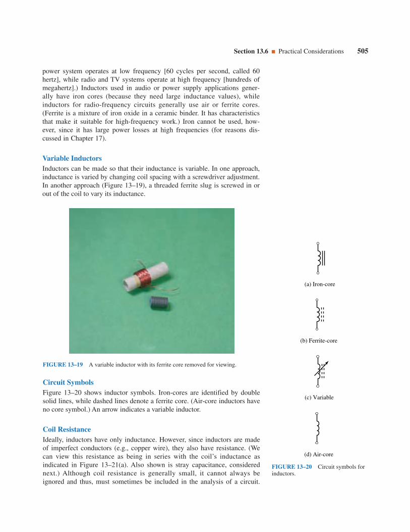
power system operates at low frequency [60 cycles per second, called 60hertz], while radio and TV systems operate at high frequency [hundreds ofmegahertz].) Inductors used in audio or power supply applications gener-ally have iron cores (because they need large inductance values), whileinductors for radio-frequency circuits generally use air or ferrite cores.(Ferrite is a mixture of iron oxide in a ceramic binder. It has characteristicsthat make it suitable for high-frequency work.) Iron cannot be used, how-ever, since it has large power losses at high frequencies (for reasons dis-cussed in Chapter 17).
Variable InductorsInductors can be made so that their inductance is variable. In one approach,inductance is varied by changing coil spacing with a screwdriver adjustment.In another approach (Figure 13–19), a threaded ferrite slug is screwed in orout of the coil to vary its inductance.
Section 13.6 Practical Considerations 505
FIGURE 13–19 A variable inductor with its ferrite core removed for viewing.
Circuit SymbolsFigure 13–20 shows inductor symbols. Iron-cores are identified by doublesolid lines, while dashed lines denote a ferrite core. (Air-core inductors haveno core symbol.) An arrow indicates a variable inductor.
Coil ResistanceIdeally, inductors have only inductance. However, since inductors are madeof imperfect conductors (e.g., copper wire), they also have resistance. (Wecan view this resistance as being in series with the coil’s inductance asindicated in Figure 13–21(a). Also shown is stray capacitance, considerednext.) Although coil resistance is generally small, it cannot always beignored and thus, must sometimes be included in the analysis of a circuit.
(a) Iron-core
(b) Ferrite-core
(c) Variable
(d) Air-core
FIGURE 13–20 Circuit symbols forinductors.

In Section 13.7, we show how this resistance is taken into account in dcanalysis; in later chapters, you will learn how to take it into account inac analysis.
506 Chapter 13 Inductance and Inductors
(a) Equivalent circuit
Rl
Cw
L
(b) Separating coil into sections helps reduce stray capacitance
FIGURE 13–21 A ferrite-core choke.
Stray CapacitanceBecause the turns of an inductor are separated from each other by insulation,a small amount of capacitance exists from winding to winding. This capaci-tance is called stray or parasitic capacitance. Although this capacitance isdistributed from turn to turn, its effect can be approximated by lumping it asin Figure 13–21(a). The effect of stray capacitance depends on frequency. Atlow frequencies, it can usually be neglected; at high frequencies, it may haveto be taken into account. Some coils are wound in multiple sections as inFigure 13–21(b) to reduce stray capacitance.
Stray InductanceBecause inductance is due entirely to the magnetic effects of electric current,all current-carrying conductors have inductance. This means that leads oncircuit components such as resistors, capacitors, transistors, and so on, allhave inductance, as do traces on printed circuit boards and wires in cables.We call this inductance “stray inductance.” Fortunately, in many cases, thestray inductance is so small that it can be neglected.
PRACTICAL NOTES...Although stray inductance is small, it is not always negligible. In general,stray inductance will not be a problem for short wires at low to moderate fre-quencies. However, even a short piece of wire can be a problem at high fre-quencies, or a long piece of wire at low frequencies. For example, the induc-tance of just a few centimeters of conductor in a high-speed logic system maybe nonnegligible because the current through it changes at such a high rate.
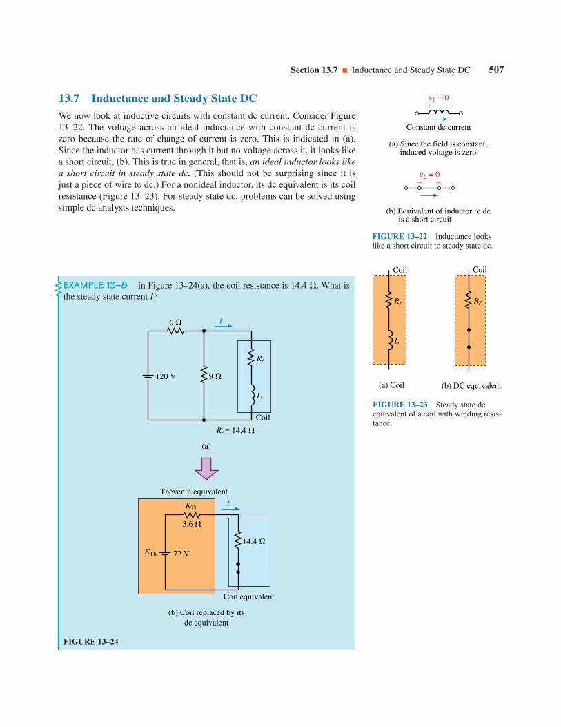
Section 13.7 Inductance and Steady State DC 507
13.7 Inductance and Steady State DCWe now look at inductive circuits with constant dc current. Consider Figure13–22. The voltage across an ideal inductance with constant dc current iszero because the rate of change of current is zero. This is indicated in (a).Since the inductor has current through it but no voltage across it, it looks likea short circuit, (b). This is true in general, that is, an ideal inductor looks likea short circuit in steady state dc. (This should not be surprising since it isjust a piece of wire to dc.) For a nonideal inductor, its dc equivalent is its coilresistance (Figure 13–23). For steady state dc, problems can be solved usingsimple dc analysis techniques.
(a) Since the field is constant,induced voltage is zero
vL = 0
Constant dc current
vL = 0
(b) Equivalent of inductor to dc is a short circuit
FIGURE 13–22 Inductance lookslike a short circuit to steady state dc.
(b) DC equivalent
Coil
Rl
FIGURE 13–23 Steady state dcequivalent of a coil with winding resis-tance.
(a) Coil
Coil
Rl
L
EXAMPLE 13–8 In Figure 13–24(a), the coil resistance is 14.4 . What isthe steady state current I?
(a)
(b) Coil replaced by itsdc equivalent
Coil equivalent
14.4
RTh
ETh
I
3.6
Thévenin equivalent
72 V
Coil
Rl
L
I
9
6
Rl = 14.4
120 V
FIGURE 13–24

508 Chapter 13 Inductance and Inductors
EXAMPLE 13–9 The resistance of coil 1 in Figure 13–25(a) is 30 andthat of coil 2 is 15 . Find the voltage across the capacitor assuming steadystate dc.
Solution Reduce the circuit as in (b).
ETh (9/15)(120) 72 V
RTh 69 3.6
Now replace the coil by its dc equivalent circuit as in (b). Thus,
I ETh/RT 72/(3.6 14.4) 4 A
(b) dc equivalent
15
Coil 2
Coil 1
30
60 V VC
R2
L2
L1
R1
60 VE VC
15
30
(a)
FIGURE 13–25
Solution Replace each coil inductance with a short circuit and the capacitorwith an open circuit. As you can see from (b), the voltage across C is thesame as the voltage across R2. Thus,
VC R1
R
2
R2
E 145
5
(60 V) 20 V

Section 13.8 Energy Stored by an Inductance 509
PRACTICEPROBLEMS 4
For Figure 13–26, find I, VC1, and VC2
in the steady state.
Answers: 10.7 A; 63 V; 31.5 V
L2
Coil 2
Coil 1
15
15 150 V
20 V
VC1
VC2
5
10
I
L1
13.8 Energy Stored by an InductanceWhen power flows into an inductor, energy is stored in its magnetic field.When the field collapses, this energy is returned to the circuit. For an idealinductor, R 0 ohm and hence no power is dissipated; thus, an ideal induc-tor has zero power loss.
To determine the energy stored by an ideal inductor, consider Figure 13–27. Power to the inductor is given by p vLi watts, where vL Ldi/dt. Bysumming this power (see next ), the energy is found to be
W 12
Li2 (J) (13–11)
where i is the instantaneous value of current. When current reaches its steadystate value I, W 1⁄2LI 2 J. This energy remains stored in the field as long asthe current continues. When the current goes to zero, the field collapses andthe energy is returned to the circuit.
∫
i
p W = Li2
vL
12
FIGURE 13–27 Energy is stored inthe magnetic field of an inductor.
EXAMPLE 13–10 The coil of Figure 13–28(a) has a resistance of 15 .When the current reaches its steady state value, the energy stored is 12 J.What is the inductance of the coil?
EWB FIGURE 13–26
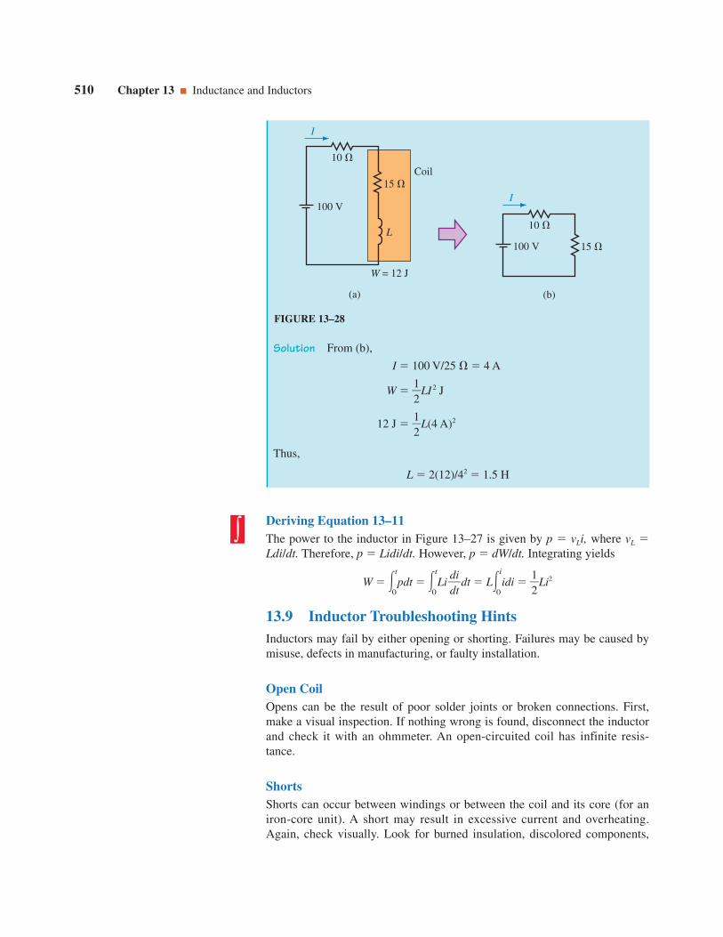
Deriving Equation 13–11The power to the inductor in Figure 13–27 is given by p vLi, where vL Ldi/dt. Therefore, p Lidi/dt. However, p dW/dt. Integrating yields
W t
0pdt t
0Li
dditdt Li
0idi
12
Li2
13.9 Inductor Troubleshooting HintsInductors may fail by either opening or shorting. Failures may be caused bymisuse, defects in manufacturing, or faulty installation.
Open CoilOpens can be the result of poor solder joints or broken connections. First,make a visual inspection. If nothing wrong is found, disconnect the inductorand check it with an ohmmeter. An open-circuited coil has infinite resis-tance.
ShortsShorts can occur between windings or between the coil and its core (for aniron-core unit). A short may result in excessive current and overheating.Again, check visually. Look for burned insulation, discolored components,
510 Chapter 13 Inductance and Inductors
Solution From (b),
I 100 V/25 4 A
W 12
LI 2 J
12 J 12
L(4 A)2
Thus,
L 2(12)/42 1.5 H
(a)
15
L
10
W = 12 J
100 V
I
(b)
15
10
100 V
I
Coil
FIGURE 13–28
∫

an acrid odor, and other evidence of overheating. An ohmmeter can be usedto check for shorts between windings and the core. However, checking coilresistance for shorted turns is often of little value, especially if only a fewturns are shorted. This is because the shorting of a few windings will notchange the overall resistance enough to be measurable. Sometimes the onlyconclusive test is to substitute a known good inductor for the suspected one.
Problems 511
PROBLEMSUnless otherwise indicated, assume ideal inductors and coils.
13.2 Induced Voltage and Inductance
1. If the flux linking a 75-turn coil changes at the rate of 3 Wb/s, what is thevoltage across the coil?
2. If 80 volts is induced when the flux linking a coil changes at a uniform ratefrom 3.5 mWb to 4.5 mWb in 0.5 ms, how many turns does the coil have?
3. Flux changing at a uniform rate for 1 ms induces 60 V in a coil. What is theinduced voltage if the same flux change takes place in 0.01 s?
13.3 Self-Inductance
4. The current in a 0.4-H inductor is changing at the rate of 200 A/s. What isthe voltage across it?
5. The current in a 75-mH inductor changes uniformly by 200 mA in 0.1 ms.What is the voltage across it?
6. The voltage across an inductance is 25 volts when the current changes at5 A/s. What is L?
7. The voltage induced when current changes uniformly from 3 amps to 5 ampsin a 10-H inductor is 180 volts. How long did it take for the current tochange from 3 to 5 amps?
8. Current changing at a uniform rate for 1 ms induces 45 V in a coil. What isthe induced voltage if the same current change takes place in 100 ms?
9. Compute the inductance of the air-core coil of Figure 13–29, given 20 cm,N 200 turns, and d 2 cm.
10. The iron-core inductor of Figure 13–30 has 2000 turns, a cross-section of1.5 1.2 inches, and an air gap of 0.2 inch. Compute its inductance.
11. The iron-core inductor of Figure 13–30 has a high-permeability core. There-fore, by Ampere’s law, NI Hgg. Because the air gap dominates, saturationdoes not occur and the core flux is proportional to the current, i.e., the fluxlinkage equals LI. In addition, since all flux passes through the coil, the fluxlinkage equals N. By equating the two values of flux linkage and usingideas from Chapter 12, show that the inductance of the coil is
L m0N
g
2Ag
13.4 Computing Induced Voltage
12. Figure 13–31 shows the current in a 0.75-H inductor. Determine vL and plotits waveform.
l
d
FIGURE 13–29
I
N
lg
FIGURE 13–30
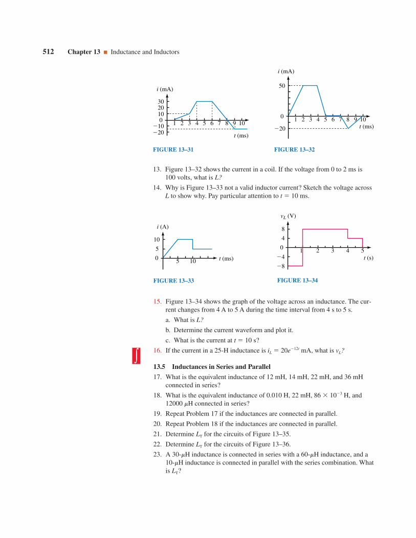
13. Figure 13–32 shows the current in a coil. If the voltage from 0 to 2 ms is100 volts, what is L?
14. Why is Figure 13–33 not a valid inductor current? Sketch the voltage acrossL to show why. Pay particular attention to t 10 ms.
512 Chapter 13 Inductance and Inductors
t (ms)
i (mA)
0
302010
1020
1 2 3 4 5 6 7 8 109 t (ms)
i (mA)
0
20
50
1 2 3 4 5 6 7 8 109
FIGURE 13–31 FIGURE 13–32
t (ms)
i (A)
0
10
5
5 10 t (s)
vL (V)
0
8
4
4
8
1 2 3 4 5
FIGURE 13–33 FIGURE 13–34
15. Figure 13–34 shows the graph of the voltage across an inductance. The cur-rent changes from 4 A to 5 A during the time interval from 4 s to 5 s.
a. What is L?
b. Determine the current waveform and plot it.
c. What is the current at t 10 s?
16. If the current in a 25-H inductance is iL 20e12t mA, what is vL?
13.5 Inductances in Series and Parallel
17. What is the equivalent inductance of 12 mH, 14 mH, 22 mH, and 36 mHconnected in series?
18. What is the equivalent inductance of 0.010 H, 22 mH, 86 103 H, and12000 mH connected in series?
19. Repeat Problem 17 if the inductances are connected in parallel.
20. Repeat Problem 18 if the inductances are connected in parallel.
21. Determine LT for the circuits of Figure 13–35.
22. Determine LT for the circuits of Figure 13–36.
23. A 30-mH inductance is connected in series with a 60-mH inductance, and a10-mH inductance is connected in parallel with the series combination. Whatis LT?
∫

24. For Figure 13–37, determine Lx.
25. For the circuits of Figure 13–38, determine L3 and L4.
26. You have inductances of 24 mH, 36 mH, 22 mH and 10 mH. Connectingthese any way you want, what is the largest equivalent inductance you canget? The smallest?
Problems 513
(a)
LT
L1 = 10 H
5 H
6 H
L2
L3
(b)
LT 6 HL23 HL1
18 H
LT 9 H 14 H
1.6 H
2 H
LT 4 H4 H
(d)
(c)
(e)
600 H
6 mH28.5 mH
LT19 mH
FIGURE 13–35

27. A 6-H and a 4-H inductance are connected in parallel. After a third induc-tance is added, LT 4 H. What is the value of the third inductance and howwas it connected?
28. Inductances of 2 H, 4 H, and 9 H are connected in a circuit. If LT 3.6 H,how are the inductors connected?
29. Inductances of 8 H, 12 H, and 1.2 H are connected in a circuit. If LT 6 H,how are the inductors connected?
30. For inductors in parallel (Figure 13–39), the same voltage appears acrosseach. Thus, v L1di1/dt, v L2di2/dt, etc. Apply KCL and show that 1/LT 1/L1 1/L2 … 1/LN.
514 Chapter 13 Inductance and Inductors
14 H
LT
1.2 H
18 H
12 H1.8 H
1.4 H4 H
18.7 H4 H
1 H
11 H
(b)
6 H
6 H
27 H
LT
1 H
4 H 2 H
18 H
2 H
(a)
FIGURE 13–36
18 H
2 H
LT = 6 HLx6 H
5 H
1.5 H L3 = 4L4
6 HL411.25 H
(a)
18 H
12.4 H L4 = 4L3L3
27 H
(b)
FIGURE 13–37
FIGURE 13–38
L2L1 L3 LN
i
i1 i2 i3 iN
v
v
v
v
v
FIGURE 13–39

31. By combining elements, reduce each of the circuits of Figure 13–40 to theirsimplest form.
Problems 515
(a)
1 H
4.5 µF
7 µF
2 µF
(c)
(b)
3 H
6 H 2 µF
8 µF
4 H
6 H
10 µF
10 µF
5 µF
10
(d)
40 H
10 H 60 µF
30 µF
10
40
FIGURE 13–40
13.7 Inductance and Steady State DC
32. For each of the circuits of Figure 13–41, the voltages and currents havereached their final (steady state) values. Solve for the quantities indicated.
3 H1 H
(a) Find E
11
6 4
E
4 A
6 H
3 H
(b) Find Rx
6
Rx
9 4.5
18 V 13.5 V
+
−
FIGURE 13–41
13.8 Energy Stored by an Inductance
33. Find the energy stored in the inductor of Figure 13–42.

34. In Figure 13–43, L1 2L2. The total energy stored is WT 75 J. Find L1
and L2.
13.9 Inductor Troubleshooting Hints
35. In Figure 13–44, an inductance meter measures 7 H. What is the likelyfault?
516 Chapter 13 Inductance and Inductors
Rl 10
L4 H
20
5
6
Coil
40 V
4
L2
11 5 L1
100 V
FIGURE 13–42 FIGURE 13–43
2 H7 H
3 H 5 H
L2 L4
L3L1
H
FIGURE 13–44
36. Referring to Figure 13–45, an inductance meter measures LT 8 mH. Whatis the likely fault?
5 mH 11 mH
2 mH
6 mH
L1
L4
L2 L3LT
FIGURE 13–45
In-Process Learning Check 1
1. Both a and b. Current cannot change instantaneously.
2. 600 Wb-turns
3. 30 V
4. 300 V
In-Process Learning Check 2
1. 28 mH
2. 9 times
In-Process Learning Check 3
1. 87.5 V
2. Rate of change of current is the same; 20 V
Answers to In-Process Learning Checks 517
ANSWERS TO IN-PROCESSLEARNING CHECKS

OBJECTIVES
After studying this chapter, you will beable to
• explain why transients occur in RL cir-cuits,
• explain why an inductor looks like anopen circuit when first energized,
• compute time constants for RL circuits,
• compute voltage and current transientsin RL circuits during the current buildupphase,
• compute voltage and current transientsin RL circuits during the current decayphase,
• solve moderately complex RL transientproblems using circuit simplificationtechniques,
• solve RL transient problems using Elec-tronics Workbench and PSpice.
KEY TERMS
Continuity of Current
De-energizing Transient
Energizing Transient
Initial Condition Circuit
RL Transients
Time Constant
OUTLINE
Introduction
Current Buildup Transients
Interrupting Current in an Inductive Circuit
De-energizing Transients
More Complex Circuits
RL Transients Using Computers
Inductive Transients14

In Chapter 11, you learned that transients occur in capacitive circuits becausecapacitor voltage cannot change instantaneously. In this chapter, you will
learn that transients occur in inductive circuits because inductor current cannotchange instantaneously. Although the details differ, you will find that many ofthe basic ideas are the same.
Inductive transients result when circuits containing inductance are dis-turbed. More so than capacitive transients, inductive transients are potentiallydestructive and dangerous. For example, when you break the current in an induc-tive circuit, an extremely large and damaging voltage may result.
In this chapter, we study basic RL transients. We look at transients duringcurrent buildup and decay and learn how to calculate the voltages and currentsthat result.
519
CHAPTER PREVIEW
PUTTING IT INPERSPECTIVE
Inductance, the Dual of Capacitance
INDUCTANCE IS THE DUAL of capacitance. This means that the effect that induc-tance has on circuit operation is identical with that of capacitance if you inter-change the term current for voltage, open circuit for short circuit, and so on. Forexample, for simple dc transients, current in an RL circuit has the same form asvoltage in an RC circuit: they both rise to their final value exponentially accord-ing to 1 et/t. Similarly, voltage across inductance decays in the same manneras current through capacitance, i.e., according to et/t.
Duality applies to steady state and initial condition representations as well.To steady state dc, for example, a capacitor looks like an open circuit, while aninductor looks like a short circuit. Similarly, the dual of a capacitor that lookslike a short circuit at the instant of switching is an inductor that looks like anopen circuit. Finally, the dual of a capacitor that has an initial condition of V0
volts is an inductance with an initial condition of I0 amps.The principle of duality is helpful in circuit analysis as it lets you transfer
the principles and concepts learned in one area directly into another. You willfind, for example, that many of the ideas learned in Chapter 11 reappear here intheir dual form.

14.1 IntroductionAs you saw in Chapter 11, when a circuit containing capacitance is dis-turbed, voltages and currents do not change to their new values immedi-ately, but instead pass through a transitional phase as the circuit capaci-tance charges or discharges. The voltages and currents during thistransitional interval are called transients. In a dual fashion, transientsoccur when circuits containing inductances are disturbed. In this case,however, transients occur because current in inductance cannot changeinstantaneously.
To get at the idea, consider Figure 14–1. In (a), we see a purely resis-tive circuit. At the instant the switch is closed, current jumps from 0 to E/Ras required by Ohm’s law. Thus, no transient (i.e., transitional phase)occurs because current reaches its final value immediately. Now consider(b). Here, we have added inductance. At the instant the switch is closed, acounter emf appears across the inductance. This voltage attempts to stopthe current from changing and consequently slows its rise. Current thusdoes not jump to E/R immediately as in (a), but instead climbs graduallyand smoothly as in (b). The larger the inductance, the longer the transitiontakes.
520 Chapter 14 Inductive Transients
FIGURE 14–1 Transient due to inductance. Adding inductance to a resistive circuitslows the current rise and fall, thus creating a transient.
Continuity of CurrentAs Figure 14–1(b) illustates, current through an inductance cannot changeinstantaneously, i.e., it cannot jump abruptly from one value to another, butmust be continuous at all values of time. This observation is known as thestatement of continuity of current for inductance. You will find this state-ment of great value when analyzing circuits containing inductance. We willuse it many times in what follows.
The continuity statement forinductor current has a soundmathematical basis. Recall,induced voltage is proportionalto the rate of change of current.In calculus notation,
vL Lddit
This means that the faster thatcurrent changes, the larger theinduced voltage. If inductor cur-rent could change from onevalue to another instantaneouslyas in Figure 14–1(a), its rate ofchange (i.e., di/dt) would be infi-nite and hence the induced volt-age would be infinite. But infi-nite voltage is not possible.Thus, inductor current cannotchange instantaneously.
NOTES...
(a) No transient occurs in apurely resistive circuit
RE i
i
t0
ER
(b ) Adding inductance causesa transient to appear.
R is held constant here
R
E vL = L
L didt
i
i
t0
ER
Final (steady state) value
Increasing L

Inductor VoltageNow consider inductor voltage. When the switch is open as in Figure 14–2(a), the current in the circuit and voltage across L are both zero. Now closethe switch. Immediately after the switch is closed, the current is still zero,(since it cannot change instantaneously). Since vR Ri, the voltage across Ris also zero and thus the full source voltage appears across L as shown in (b).The inductor voltage therefore jumps from 0 V just before the switch isclosed to E volts just after. It then decays to zero, since, as we saw in Chap-ter 13, the voltage across inductance is zero for steady state dc. This is indi-cated in (c).
Section 14.1 Introduction 521
FIGURE 14–2 Voltage across L.
Open-Circuit Equivalent of an InductanceConsider again Figure 14–2(b). Note that just after the switch is closed, theinductor has voltage across it but no current through it. It therefore momen-tarily looks like an open circuit. This is indicated in Figure 14–3. This obser-vation is true in general, that is, an inductor with zero initial current lookslike an open circuit at the instant of switching. (Later, we extend this state-ment to include inductors with nonzero initial currents.)
Initial Condition CircuitsVoltages and currents in circuits immediately after switching must some-times be calculated. These can be determined with the aid of the open-circuitequivalent. By replacing inductances with open circuits, you can see what acircuit looks like just after switching. Such a circuit is called an initial con-dition circuit.
FIGURE 14–3 Inductor with zeroinitial current looks like an open circuitat the instant the switch is closed.
EXAMPLE 14–1 A coil and two resistors are connected to a 20-V source asin Figure 14–4(a). Determine source current i and inductor voltage vL at theinstant the switch is closed.
(a) Circuit with switchopen. Current i = 0
R
E vL = 0
i = 0
R
E L vL = E
t = 0
(b) Circuit just after theswitch has been closed.
Current is still equal to zero.Thus, vL = E
vR = Ri = 0
i = 0
(c) Voltage across L
vL
0 V
0t
EVoltagetransient
E vL = E
i = 0
vR = 0
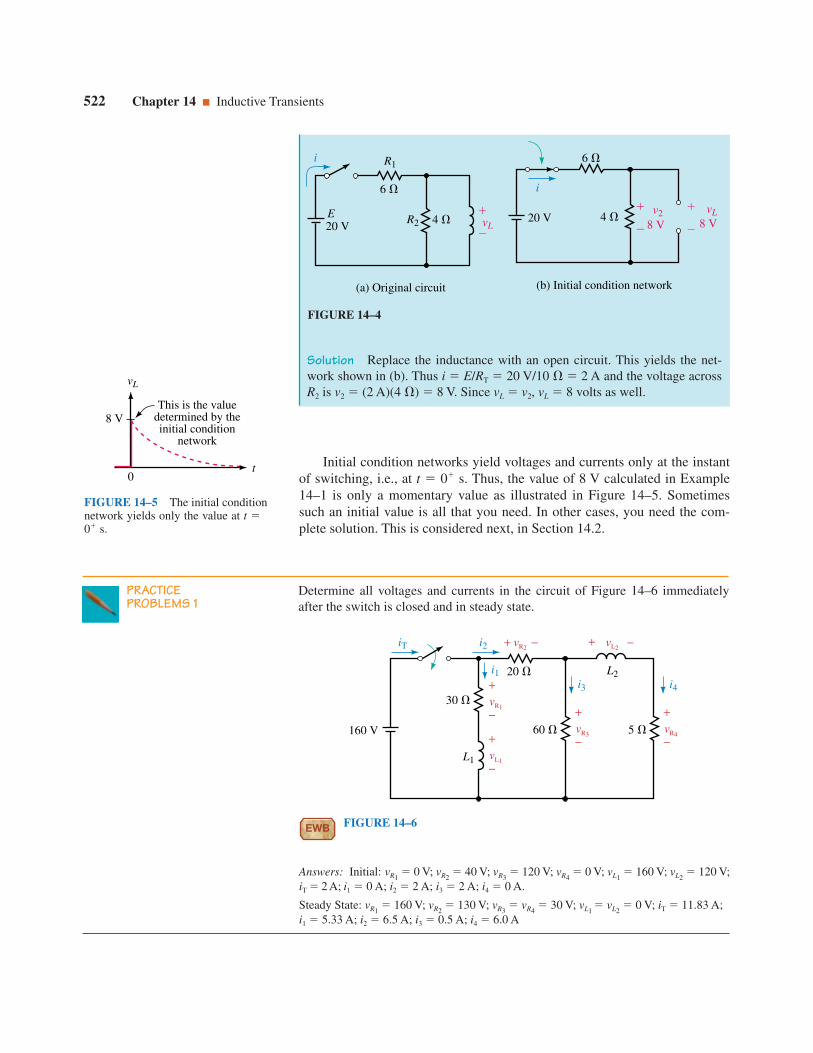
Initial condition networks yield voltages and currents only at the instantof switching, i.e., at t 0 s. Thus, the value of 8 V calculated in Example14–1 is only a momentary value as illustrated in Figure 14–5. Sometimessuch an initial value is all that you need. In other cases, you need the com-plete solution. This is considered next, in Section 14.2.
522 Chapter 14 Inductive Transients
Solution Replace the inductance with an open circuit. This yields the net-work shown in (b). Thus i E/RT 20 V/10 2 A and the voltage acrossR2 is v2 (2 A)(4 ) 8 V. Since vL v2, vL 8 volts as well.
FIGURE 14–4
vL
0t
8 VThis is the value
determined by theinitial condition
network
FIGURE 14–5 The initial conditionnetwork yields only the value at t 0 s.
PRACTICEPROBLEMS 1
Determine all voltages and currents in the circuit of Figure 14–6 immediatelyafter the switch is closed and in steady state.
20
30
5 60
iT
160 V
i2
i1i3 i4
L2
L1
+ vR2 −
+
−vR1
+
+
−
−
vL1
+
−vR3
+
−vR4
vL2
Answers: Initial: vR1 0 V; vR2
40 V; vR3 120 V; vR4
0 V; vL1 160 V; vL2
120 V;iT 2 A; i1 0 A; i2 2 A; i3 2 A; i4 0 A.
Steady State: vR1 160 V; vR2
130 V; vR3 vR4
30 V; vL1 vL2
0 V; iT 11.83 A;i1 5.33 A; i2 6.5 A; i3 0.5 A; i4 6.0 A
EWB FIGURE 14–6
R2 4 E
6
vL20 V
i R1
(a) Original circuit
4
6
i
vL8 V20 V
v2
8 V
(b) Initial condition network
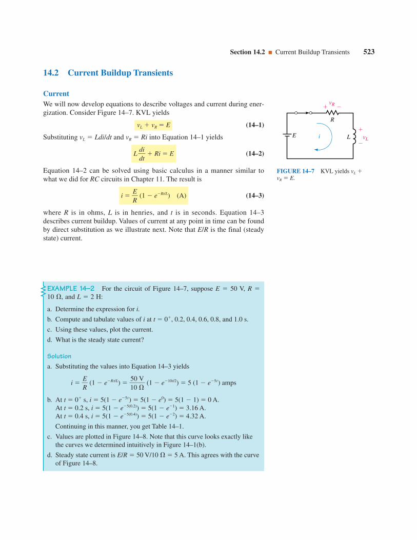
14.2 Current Buildup Transients
CurrentWe will now develop equations to describe voltages and current during ener-gization. Consider Figure 14–7. KVL yields
vL vR E (14–1)
Substituting vL Ldi/dt and vR Ri into Equation 14–1 yields
L ddit Ri E (14–2)
Equation 14–2 can be solved using basic calculus in a manner similar towhat we did for RC circuits in Chapter 11. The result is
i ER
(1 eRt/L) (A) (14–3)
where R is in ohms, L is in henries, and t is in seconds. Equation 14–3describes current buildup. Values of current at any point in time can be foundby direct substitution as we illustrate next. Note that E/R is the final (steadystate) current.
Section 14.2 Current Buildup Transients 523
R
E vL
vR
i L
FIGURE 14–7 KVL yields vL vR E.
EXAMPLE 14–2 For the circuit of Figure 14–7, suppose E 50 V, R 10 , and L 2 H:
a. Determine the expression for i.
b. Compute and tabulate values of i at t 0, 0.2, 0.4, 0.6, 0.8, and 1.0 s.
c. Using these values, plot the current.
d. What is the steady state current?
Solutiona. Substituting the values into Equation 14–3 yields
i ER
(1 eRt/L) 1500
V (1 e10t/2) 5 (1 e5t) amps
b. At t 0 s, i 5(1 e5t) 5(1 e0) 5(1 1) 0 A.At t 0.2 s, i 5(1 e5(0.2)) 5(1 e1) 3.16 A.At t 0.4 s, i 5(1 e5(0.4)) 5(1 e2) 4.32 A.
Continuing in this manner, you get Table 14–1.
c. Values are plotted in Figure 14–8. Note that this curve looks exactly likethe curves we determined intuitively in Figure 14–1(b).
d. Steady state current is E/R 50 V/10 5 A. This agrees with the curveof Figure 14–8.

Circuit VoltagesWith i known, circuit voltages can be determined. Consider voltage vR. SincevR Ri, when you multiply R times Equation 14–3, you get
vR E(1 eRt/L) (V) (14–4)
Note that vR has exactly the same shape as the current. Now consider vL.Voltage vL can be found by subtracting vR from E as per Equation 14–1:
vL E vR E E(1 eRt/L) E E EeRt/L
Thus,
vL EeRt/L (14–5)
An examination of Equation 14–5 shows that vL has an initial value of E att 0 s and then decays exponentially to zero. This agrees with our earlierobservation in Figure 14–2(c).
524 Chapter 14 Inductive Transients
TABLE 14–1
Time Current
0 00.2 3.160.4 4.320.6 4.750.8 4.911.0 4.97
i (A)
t (s)
1.0
0.2 0.4 0.6 0.8 1.00
0
2.0
3.0
4.0
5.0
Final value = = 5 A
i = 5(1 − e−5t)A
ER3.16
4.324.75 4.91 4.97
EWB FIGURE 14–8 Current buildup transient.
EXAMPLE 14–3 Repeat Example 14–2 for voltage vL.
Solutiona. From equation 14–5,
vL EeRt/L 50e5t volts

Time ConstantIn Equations 14–3 to 14–5 L/R is the time constant of the circuit.
t RL
(s) (14–6)
c. Yes
d. i and vR have the shape shown in Figure 14–8, while vL has the shape shown in Figure14–9, with values according to the table shown in b.
Section 14.2 Current Buildup Transients 525
TABLE 14–2
Time (s) Voltage (V)
0 50.00.2 18.40.4 6.770.6 2.490.8 0.9161.0 0.337
vL (V)
t (s)
10
0.2 0.4 0.6 0.8 1.00
20
30
40
50
Initial value = E
vL = 50e−5t V
18.4
6.772.49 0.916 0.337
EWB FIGURE 14–9 Inductorvoltage transient.
PRACTICEPROBLEMS 2
For the circuit of Figure 14–7, with E 80 V, R 5 k, and L 2.5 mH:
a. Determine expressions for i, vL, and vR.
b. Compute and tabulate values at t 0, 0.5, 1.0, 1.5, 2.0, and 2.5 ms.
c. At each point in time, does vL vR E?
d. Plot i, vL, and vR using the values computed in (b).
Answers: a. i 16(1 e2106t) mA; vL 80e2106t V; vR 80(1 e2106t)
b.t (s) vL (V) iL (mA) vR (V)
0 80 0 00.5 29.4 10.1 50.61.0 10.8 13.8 69.21.5 3.98 15.2 76.02.0 1.47 15.7 78.52.5 0.539 15.9 79.5
b. At t 0 s, vL 50e5t 50e0 50(1) 50 V.At t 0.2 s, vL 50e5(0.2) 50e1 18.4 V.At t 0.4 s, vL 50e5(0.4) 50e2 6.77 V.
Continuing in this manner, you get Table 14–2.
c. The waveform is shown in Figure 14–9.
d. Steady state voltage is 0 V, as you can see in Figure 14–9.

Note that t has units of seconds. (This is left as an exercise for the student.)Equations 14–3, 14–4, and 14–5 may now be written as
i ER
(1 et/t) (A) (14–7)
vL Eet/t (V) (14–8)
vR E(1 et/t) (V) (14–9)
Curves are plotted in Figure 14–10 versus time constant. As expected, transi-tions take approximately 5t; thus, for all practical purposes, inductive tran-sients last five time constants.
526 Chapter 14 Inductive TransientsPe
rcen
t
t 2 3 4 50
100i or vR
vL
99.398.2
63.2
95.086.5
13.54.98 1.83 0.674
36.8
Final value
Final value
FIGURE 14–10 Universal time con-stant curves for the RL circuit.
EXAMPLE 14–4 In a circuit where L 2 mH, transients last 50 ms. Whatis R?
Solution Transients last five time constants. Thus, t 50 ms/5 10 ms.Now t L/R. Therefore, R L/t 2 mH/10 ms 200 .
EXAMPLE 14–5 For an RL circuit, i 40(1 e5t) A and vL 100e5t V.
a. What are E and t?
b. What is R?
c. Determine L.
Solutiona. From Equation 14–8, vL Eet/t 100e5t. Therefore, E 100 V and
t 15
0.2s.
b. From Equation 14–7,
i ER
(1 et/t) 40(1 e5t).
Therefore, E/R 40 A and R E/40 A 100 V/40 A 2.5 .
c. t L/R. Therefore, L Rt (2.5)(0.2) 0.5 H.
It is sometimes easier to solve problems using the time constant curvesthan it is to solve the equation. (Be sure to convert curve percentages to adecimal value first, e.g., 63.2% to 0.632.) To illustrate, consider the problemof Examples 14–2 and 14–3. From Figure 14–10 at t t 0.2 s, i 0.632E/R and vL 0.368E. Thus, i 0.632(5 A) 3.16 A and vL 0.368(50 V) 18.4 V as we found earlier.
The effect of inductance and resistance on transient duration is shown inFigure 14–11. The larger the inductance, the longer the transient for a givenresistance. Resistance has the opposite effect: for a fixed inductance, the
vL
t
Increasing L (fixed R)Increasing R (fixed L)
FIGURE 14–11 Effect of R and L ontransient duration.
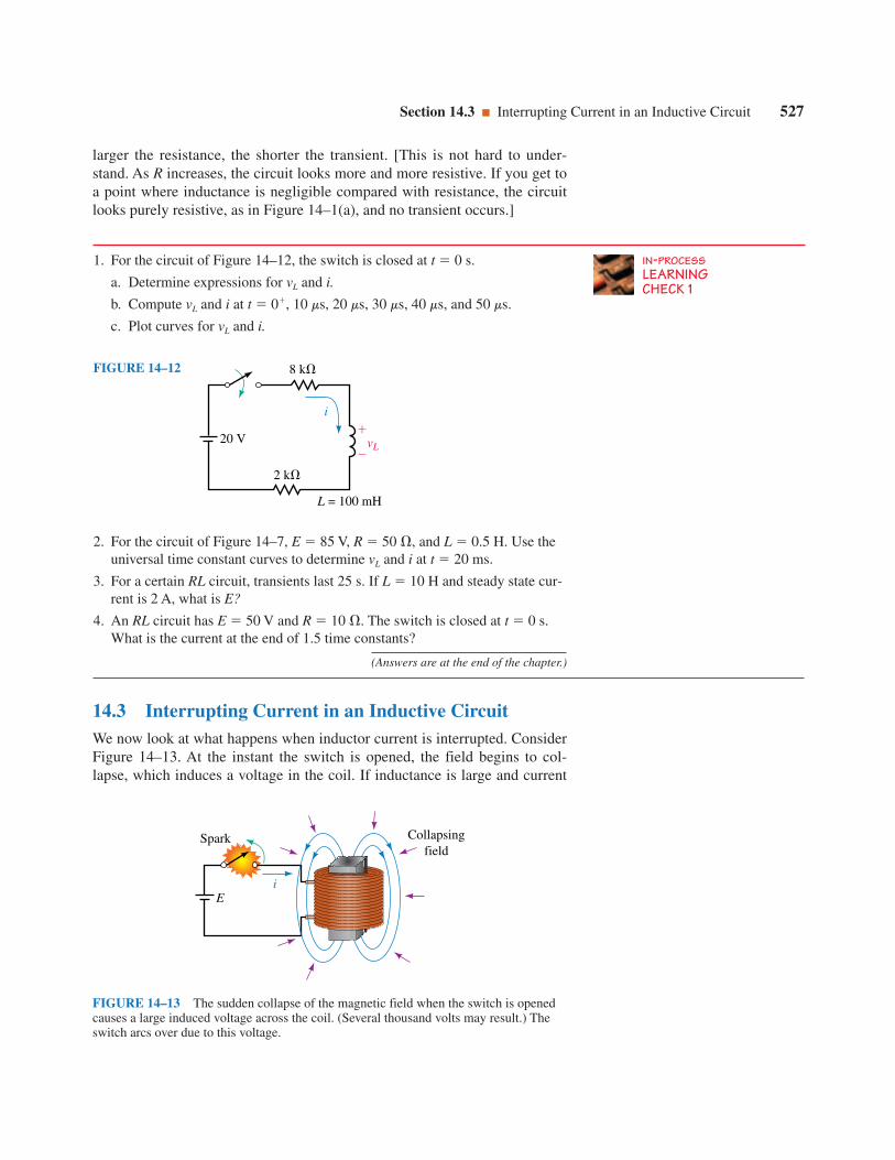
larger the resistance, the shorter the transient. [This is not hard to under-stand. As R increases, the circuit looks more and more resistive. If you get toa point where inductance is negligible compared with resistance, the circuitlooks purely resistive, as in Figure 14–1(a), and no transient occurs.]
Section 14.3 Interrupting Current in an Inductive Circuit 527
IN-PROCESSLEARNINGCHECK 1
1. For the circuit of Figure 14–12, the switch is closed at t 0 s.
a. Determine expressions for vL and i.
b. Compute vL and i at t 0, 10 ms, 20 ms, 30 ms, 40 ms, and 50 ms.
c. Plot curves for vL and i.
FIGURE 14–12 8 k
2 k
20 V vL
i
L = 100 mH
2. For the circuit of Figure 14–7, E 85 V, R 50 , and L 0.5 H. Use theuniversal time constant curves to determine vL and i at t 20 ms.
3. For a certain RL circuit, transients last 25 s. If L 10 H and steady state cur-rent is 2 A, what is E?
4. An RL circuit has E 50 V and R 10 . The switch is closed at t 0 s.What is the current at the end of 1.5 time constants?
(Answers are at the end of the chapter.)
14.3 Interrupting Current in an Inductive CircuitWe now look at what happens when inductor current is interrupted. ConsiderFigure 14–13. At the instant the switch is opened, the field begins to col-lapse, which induces a voltage in the coil. If inductance is large and current
E
Collapsingfield
i
Spark
FIGURE 14–13 The sudden collapse of the magnetic field when the switch is openedcauses a large induced voltage across the coil. (Several thousand volts may result.) Theswitch arcs over due to this voltage.

is high, a great deal of energy is released in a very short time, creating ahuge voltage that may damage equipment and create a shock hazard. (Thisinduced voltage is referred to as an inductive kick.) For example, abruptlybreaking the current through a large inductor (such as a motor or generatorfield coil) can create voltage spikes up to several thousand volts, a valuelarge enough to draw long arcs as indicated in Figure 14–13. Even moderatesized inductances in electronic systems can create enough voltage to causedamage if protective circuitry is not used.
The dynamics of the switch flashover are not hard to understand. Whenthe field collapses, the voltage across the coil rises rapidly. Part of this volt-age appears across the switch. As the switch voltage rises, it quickly exceedsthe breakdown strength of air, causing a flashover between its contacts. Oncestruck, the arc is easily maintained, as it creates ionized gases that provide arelatively low resistance path for conduction. As the contacts spread apart,the arc elongates and eventually disappears as the coil energy is dissipatedand coil voltage drops below that required to sustain the arc.
There are several important points to note here:
1. Flashovers, as in Figure 14–13, are generally undesirable. However, theycan be controlled through proper engineering design. (One way is to use adischarge resistor, as in the next example; another way is to use a diode,as you will see in your electronics course.)
2. On the other hand, the large voltages created by breaking inductive currentshave their uses. One is in the ignition system of automobiles, where currentin the primary winding of a transformer coil is interrupted at the appropriatetime by a control circuit to create the spark needed to fire the engine.
3. It is not possible to rigorously analyze the circuit of Figure 14–13 becausethe resistance of the arc changes as the switch opens. However, the mainideas can be established by studying circuits using fixed resistors as wesee next.
The Basic IdeasWe begin with the circuit of Figure 14–14. Assume the switch is closed andthe circuit is in steady state. Since the inductance looks like a short circuit[Figure 14–15(a)], its current is iL 120 V/30 4 A.
528 Chapter 14 Inductive Transients
The intuitive explanation herehas a sound mathematical basis.Recall, back emf (induced volt-age) across a coil is given by
vL Lddit L
it
where i is the change in cur-rent and t is the time intervalover which the change takesplace. When you open theswitch, current begins to dropimmediately toward zero. Sincei is finite, and t → 0, the volt-age across L rises to a very largevalue, causing a flashover tooccur. After the flashover, cur-rent has a path through which todecay and thus t, althoughsmall, no longer approacheszero. The result is a large butfinite voltage spike across L.
NOTES...
R2
R1
E
SW
Dischargeresistor L vL
FIGURE 14–14 Discharge resistorR2 helps limit the size of the inducedvoltage.
(a) Circuit just beforethe switch is opened
R2 600
iL = 4 A
R1 = 30
i2 = 0.2 A
vL = 0120 V
SW
(b) Circuit just after SW is opened.Since coil voltage polarity is opposite
to that shown, vL is negative
R1
R2
4 A
SW
vL
vR1 = 120 V
vR2
vSW
2520 V2400 V
EWB FIGURE 14–15 Circuit of Figure 14–14 immediately before and after the switchis opened. Coil voltage changes abruptly from 0 V to 2520 V for this example.

Now open the switch. Just prior to opening the switch, iL 4 A; there-fore, just after opening the switch, it must still be 4 A. As indicated in (b),this 4 A passes through resistances R1 and R2, creating voltages vR1
4 A 30 120 V and vR2
4 A 600 2400 V with the polarity shown.From KVL, vL vR1
vR2 0. Therefore at the instant the switch is opened,
vL (vR1 vR2
) 2520 volts
appears across the coil, yielding a negative voltage spike as in Figure 14–16.Note that this spike is more than 20 times larger than the source voltage. Aswe see in the next section, the size of this spike depends on the ratio of R2 toR1; the larger the ratio, the larger the voltage.
Consider again Figure 14–15. Note that current i2 changes abruptly from0.2 A just prior to switching to 4 A just after. This is permissible, however,since i2 does not pass through the inductor and only currents through induc-tance cannot change abruptly.
Section 14.4 De-energizing Transients 529
vL
0
Voltage at theinstant the switchis opened
t
2520 V
iL vL
FIGURE 14–16 Voltage spike for thecircuit of Figure 14–14. This voltage ismore than 20 times larger than thesource voltage.
PRACTICEPROBLEMS 3
Figure 14–16 shows the voltage across the coil of Figure 14–14. Make a similarsketch for the voltage across the switch and across resistor R2. Hint: Use KVL tofind vSW and vR2
.
Answer: vSW: With the switch closed, vSW 0 V; When the switch is opened, vSW jumps to2520 V, then decays to 120 V. vR2
: Identical to Figure 14–16 except that vR2begins at
2400 V instead of 2520 V.
Inductor Equivalent at SwitchingFigure 14–17 shows the current through L of Figure 14–15. Because the cur-rent is the same immediately after switching as it is immediately before, it isconstant over the interval from t 0 s to t 0 s. Since this is true in gen-eral, we see that an inductance with an initial current looks like a currentsource at the instant of switching. Its value is the value of the current atswitching. This is shown in Figure 14–18.
iL
t0
4 amps
Switchopened here
FIGURE 14–17 Inductor current forthe circuit of Figure 14–15.
(a) Current at switching
iL = I0 I0
(b) Current source equivalent
FIGURE 14–18 An inductor carrying current looks like a current source at the instantof switching.
14.4 De-energizing TransientsWe now look at equations for the voltages and currents described in the pre-vious section. As we go through this material, you should focus on the basicprinciples involved, rather than just the resulting equations. You will probably

forget formulas, but if you understand principles, you should be able to rea-son your way through many problems using just the basic current and volt-age relationships.
Consider Figure 14–19(a). Let the initial current in the inductor bedenoted as I0 amps. Now open the switch as in (b). KVL yields vL vR1
vR2
0. Substituting vL Ldi/dt, vR1 R1i, and vR2
R2i yields Ldi/dt (R1 R2)i 0. Now using calculus, it can be shown that
i I0et/t (A) (14–10)
where
t RL
T
R1
LR2
(s) (14–11)
is the time constant of the discharge circuit. If the circuit is in steady statebefore the switch is opened, initial current I0 E/R1 and Equation 14–10becomes
i RE
1
et/t (A) (14–12)
530 Chapter 14 Inductive Transients
R2
R1
vL
vR2
R2
R1
E
SW
L
i
vR1
i2
i = I0
(a) Before the switchis opened
(b) Decay circuit
FIGURE 14–19 Circuit for studyingdecay transients.
EXAMPLE 14–6 For Figure 14–19(a), assume the current has reachedsteady state with the switch closed. Suppose that E 120 V, R1 30 , R2 600 , and L 126 mH:
a. Determine I0.
b. Determine the decay time constant.
c. Determine the equation for the current decay.
d. Compute the current i at t 0 s and t 0.5 ms.
Solutiona. Consider Figure 14–19(a). Since the circuit is in a steady state, the induc-
tor looks like a short circuit to dc. Thus, I0 E/R1 4 A.
b. Consider Figure 14–19(b). t L/(R1 R2) 126 mH/630 0.2 ms.
c. i I0et/t 4et/0.2 ms A.
d. At t 0 s, i 4e0 4 A.
At t 0.5 ms, i 4e0.5 ms/0.2 ms 4e2.5 0.328 A.
Now consider voltage vL. It can be shown to be
vL V0et/t (14–13)
where V0 is the voltage across L just after the switch is opened. Letting i I0
in Figure 14–19(b), you can see that V0 I0(R1 R2) I0RT. ThusEquation 14–13 can be written as
vL I0RTet/t (14–14)

Finally, if the current has reached steady state before the switch is opened,I0 E/R1, and Equation 14–14 becomes
vL E1 R
R2
1
et/t (14–15)
Note that vL starts at V0 volts (which is negative) and decays to zero as shownin Figure 14–20.
Now consider the resistor voltages. Each is the product of resistancetimes current (Equation 14–10). Thus,
vR1 R1I0e
t/t (14–16)
and
vR2 R2I0e
t/t (14–17)
If current has reached steady state before switching, these become
vR1 Eet/t (14–18)
and
vR2
R
R2
1
Eet/t (14–19)
Substituting the values of Example 14–6 into these equations, we get for thecircuit of Figure 14–19 vL 2520et/0.2 ms V, vR1
120et/0.2 ms V and vR2
2400et/0.2 ms V. These can also be written as vL 2520e5000t V and so on ifdesired.
Decay problems can also be solved using the decay portion of the uni-versal time constant curves shown in Figure 14–10.
Section 14.5 More Complex Circuits 531
vL
vL = V0e
0t
V0
t/'
FIGURE 14–20 Inductor voltageduring decay phase. V0 is negative.
EXAMPLE 14–7 For Figure 14–19, let E 120 V, R1 40 and R2 20 .The circuit is in steady state with the switch closed. Use Figure 14–10 to findi and vL at t 2 t after the switch is opened.
Solution I0 E/R1 3 A. At t 2 t, current will have decayed to 13.5%.Therefore, i 0.135I0 0.405 A and vL (R1 R1)i (60 )(0.405 A) 24.3 V. (Alternately, V0 (3 A)(60 ) 180 V. At t 2 t, this hasdecayed to 13.5%. Therefore, vL 0.135(180 V) 24.3 V as above.)
14.5 More Complex CircuitsThe equations developed so far apply only to circuits of the forms of Figures14–7 or 14–19. Fortunately, many circuits can be reduced to these formsusing circuit reduction techniques such as series and parallel combinations,source conversions, Thévenin’s theorem, and so on.

532 Chapter 14 Inductive Transients
EXAMPLE 14–8 Determine iL for the circuit of Figure 14–21(a) if L 5 H.
Solution The circuit can be reduced to its Thévenin equivalent (b) as yousaw in Chapter 11 (Section 11.5). For this circuit, t L/RTh 5 H/200 25 ms. Now apply Equation 14–7. Thus,
iL E
RT
T
h
h
(1 et/t) 2
4
0
0
0 (1 et/25 ms) 0.2 (1 e40t) (A)
240
800
R1
a b
R2200
R3104 R4E
L
iL
100 V
(b) Thévenin equivalent
(a) Circuit
200
RTh
ETh
L
iL40 V
FIGURE 14–21
EXAMPLE 14–9 For the circuit of Example 14–8, at what time does cur-rent reach 0.12 amps?
SolutioniL 0.2(1 e40t) (A)
Thus,
0.12 0.2(1 e40t) (Figure 14–22)
0.6 1 e40t
e40t 0.4

A Note About Time ScalesUntil now, we have considered energization and de-energization phases sep-arately. When both occur in the same problem, we must clearly define whatwe mean by time. One way to handle this problem (as we did with RC cir-cuits) is to define t 0 s as the beginning of the first phase and solve forvoltages and currents in the usual manner, then shift the time axis to thebeginning of the second phase, redefine t 0 s and then solve the secondpart. This is illustrated in Example 14–10. Note that only the first time scaleis shown explicitly on the graph.
Section 14.5 More Complex Circuits 533
Taking the natural log of both sides,
ln e40t ln 0.4
40t 0.916
t 22.9 ms
FIGURE 14–22
iL (A)
Timet
0.12
0
0.2
PRACTICEPROBLEMS 4
1. For the circuit of Figure 14–21, let E 120 V, R1 600 , R2 3 k, R3 2 k, R4 100 , and L 0.25 H:
a. Determine iL and sketch it.
b. Determine vL and sketch it.
2. Let everything be as in Problem 1 except L. If iL 0.12 A at t 20 ms, whatis L?
Answers:1. a. 160(1 e2000t) mA b. 80e2000 t V. iL climbs from 0 to 160 mA with the wave-
shape of Figure 14–1(b), reaching steady state in 2.5 ms. vL looks like Figure 14–2(c).It starts at 80 V and decays to 0 V in 2.5 ms.
2. 7.21 H
EXAMPLE 14–10 Refer to the circuit of Figure 14–23:
a. Close the switch at t 0 and determine equations for iL and vL.
b. At t 300 ms, open the switch and determine equations for iL and vL dur-ing the decay phase.
c. Determine voltage and current at t 100 ms and at t 350 ms.
d. Sketch iL and vL. Mark the points from (c) on the sketch.

534 Chapter 14 Inductive Transients
Solutiona. Convert the circuit to the left of L to its Thévenin equivalent. As indicated
in Figure 14–24(a), RTh 6030 80 100 . From (b), ETh V2,where
V2 (10 A)(20 ) 200 V
80
R3
R2 60
L = 5 H
R1 30 10 A iL
vL
EWB FIGURE 14–23
The Thévenin equivalent circuit is shown in Figure 14–25(a). t L/RTh 50 ms. Thus during current buildup,
iL E
RT
T
h
h
(1 et/t) 2
1
0
0
0
0 (1 et/50 ms) 2 (1 e20t) A
vL EThet/t 200 e20t V
b. Current build-up is sketched in Figure 14–25(b). Since 5t 250 ms,current is in steady state when the switch is opened at 300 ms. Thus I0
80
R3
R2 60 R1 30 RTh = 100
20
(a)
(b)
10 A
ETh = V2 = 200 V
80
V220
R1 || R2
FIGURE 14–24
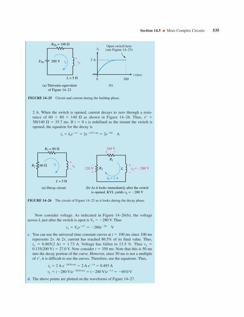
Section 14.5 More Complex Circuits 535
2 A. When the switch is opened, current decays to zero through a resis-tance of 60 80 140 as shown in Figure 14–26. Thus, t 5H/140 35.7 ms. If t 0 s is redefined as the instant the switch isopened, the equation for the decay is
iL I0et/t 2et/35.7 ms 2e28t A
Now consider voltage. As indicated in Figure 14–26(b), the voltageacross L just after the switch is open is V0 280 V. Thus
vL V0et/t 280e28t V
c. You can use the universal time constant curves at t 100 ms since 100 msrepresents 2t. At 2t, current has reached 86.5% of its final value. Thus,iL 0.865(2 A) 1.73 A. Voltage has fallen to 13.5 %. Thus vL 0.135(200 V) 27.0 V. Now consider t 350 ms: Note that this is 50 msinto the decay portion of the curve. However, since 50 ms is not a multipleof t, it is difficult to use the curves. Therefore, use the equations. Thus,
iL 2 A e28(50 ms) 2 A e1.4 0.493 A
vL (280 V)e28(50 ms) (280 V)e1.4 69.0 V
d. The above points are plotted on the waveforms of Figure 14–27.
RTh = 100
vL
L = 5 H
ETh 200 V
(a) Thévenin equivalentof Figure 14–23
iL
(b)
iL
t (ms)
2 A
Open switch here(see Figure 14–23)
0 300
FIGURE 14–25 Circuit and current during the buildup phase.
(a) Decay circuit
R2
R3 = 80
60 iL
L = 5 H
vL
(b) As it looks immediately after the switchis opened. KVL yields vL = 280 V
R2
R1
I0 = 2 A
L
160 V
120 V
vL = 280 V
FIGURE 14–26 The circuit of Figure 14–23 as it looks during the decay phase.

The basic principles that we have developed in this chapter permit us tosolve problems that do not correspond exactly to the circuits of Figure 14–7and 14–19. This is illustrated in the following example.
536 Chapter 14 Inductive Transients
2.0
1.0
00 50 100 150 200 250 300 350 400 t (ms)
iL (A)
200
100
0
−100
−200
−300
50 100 150 200 250 300 350 400 t (ms)
vL (V)Switchopenedhere
−280 V
1.73 A 0.493 A
27.0 V
−69.0 V
FIGURE 14–27
EXAMPLE 14–11 The circuit of Figure 14–28(a) is in steady state with theswitch open. At t 0 s, the switch is closed.
40 10
E
L = 100 mH
iLt = 0
100 V
R2R1
(a) Steady state current with the
switch open is = 2 A100 V50
R2 = 40
L = 100 mH
vL
iL
vR2
(b) Decay circuit
' = = 2.5 msLR2
a. Sketch the circuit as it looks after the switch is closed and determine t.
b. Determine current iL at t 0 s.
c. Determine the expression for iL.
EWB FIGURE 14–28
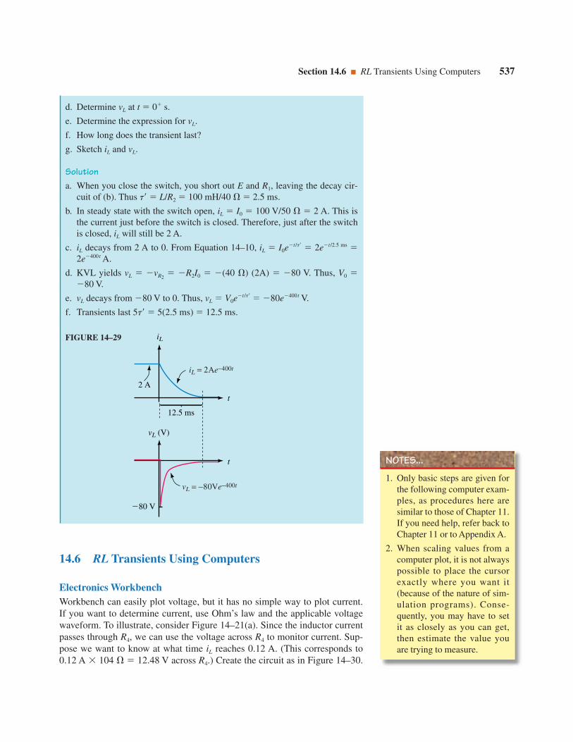
14.6 RL Transients Using Computers
Electronics WorkbenchWorkbench can easily plot voltage, but it has no simple way to plot current.If you want to determine current, use Ohm’s law and the applicable voltagewaveform. To illustrate, consider Figure 14–21(a). Since the inductor currentpasses through R4, we can use the voltage across R4 to monitor current. Sup-pose we want to know at what time iL reaches 0.12 A. (This corresponds to0.12 A 104 12.48 V across R4.) Create the circuit as in Figure 14–30.
Section 14.6 RL Transients Using Computers 537
d. Determine vL at t 0 s.
e. Determine the expression for vL.
f. How long does the transient last?
g. Sketch iL and vL.
Solutiona. When you close the switch, you short out E and R1, leaving the decay cir-
cuit of (b). Thus t L/R2 100 mH/40 2.5 ms.
b. In steady state with the switch open, iL I0 100 V/50 2 A. This isthe current just before the switch is closed. Therefore, just after the switchis closed, iL will still be 2 A.
c. iL decays from 2 A to 0. From Equation 14–10, iL I0et/t 2et/2.5 ms
2e400t A.
d. KVL yields vL vR2 R2I0 (40 ) (2A) 80 V. Thus, V0
80 V.
e. vL decays from 80 V to 0. Thus, vL V0et/t 80e400t V.
f. Transients last 5t 5(2.5 ms) 12.5 ms.
vL (V)
iL
t
t
2 A
12.5 ms
80 V
vL = −80Ve−400t
iL = 2Ae−400t
FIGURE 14–29
1. Only basic steps are given forthe following computer exam-ples, as procedures here aresimilar to those of Chapter 11.If you need help, refer back toChapter 11 or to Appendix A.
2. When scaling values from acomputer plot, it is not alwayspossible to place the cursorexactly where you want it(because of the nature of sim-ulation programs). Conse-quently, you may have to setit as closely as you can get,then estimate the value youare trying to measure.
NOTES...

Select Analysis/Transient, click Initial Conditions Set to Zero, set End Time(TSTOP) to 0.1, select Node 3, click Add, then Simulate. You should get thewaveform shown on the screen of Figure 14–30. Expand to full size, thenuse the cursor to determine the time at which voltage equals 12.48 V. Figure14–31 shows the result. Rounded to 3 figures, the answer is 22.9 ms (whichagrees with the answer we obtained earlier in Example 14–9).
538 Chapter 14 Inductive Transients
FIGURE 14–30 Electronics Workbench representation of Figure 14–21. No switch isrequired as the transient solution is initiated by software.
FIGURE 14–31 Values scaled from thewaveform of Figure 14–30.
(a) Connecting the oscilloscope (b) Expanded oscilloscope detail
FIGURE 14–32 Using the Electronics Workbench oscilloscope.
Using Electronics Workbench’s Oscilloscope
Waveforms may also be observed using Electronics Workbench’s oscillo-scope. Close the Analysis Graphs window, click the Instruments Parts bin,position the scope and connect as in Figure 14–32(a). Double click the scopeicon, set Time base to 5 ms/div, Channel A to 5 V/div and Y position to 1 (tobetter fit the trace to the screen.) Select Analysis/Analysis Options, click onthe Instruments tab, select Pause after each screen, select Initial ConditionsSet to Zero, click OK, then activate the circuit by clicking the ON/OFF powerswitch in the upper right-hand corner of the screen. The trace shown in Figure14–32(b) should appear. Click the Expand button on the oscilloscope and drag

the cursor until VA reads 12.48 volts (or as close as you can get). The corre-sponding value of time should be 22.9 ms as determined previously.
OrCAD PSpiceRL transients are handled much like RC transients. As a first example, considerFigure 14–33. The circuit is in steady state with the switch closed. At t 0, theswitch is opened. Use PSpice to plot inductor voltage and current, then use thecursor to determine values at t 100 ms. Verify manually. (Since the processis similar to that of Chapter 11, abbreviated instructions only are given.)
Section 14.6 RL Transients Using Computers 539
Preliminary: First, determine the initial current in the inductor, i.e., thecurrent I0 that exists at the instant the switch is opened. This is done by not-ing that the inductor looks like a short circuit to steady state dc. Thus, I0 12 V/ 4 3 A. Next, note that after the switch is opened, current builds upthrough R1, R2, and R3 in series. Thus, the time constant of the circuit is t L1/RT 3 H/30 0.1 s. Now proceed as follows:
• Build the circuit on the screen. Double click the inductor symbol andusing the procedure from Chapter 11, set its initial condition IC to 3A.Click the New Profile icon and name the file fig14-33. In the SimulationsSettings box, select transient analysis and set TSTOP to 0.5 (five time con-stants). Click OK.
• Click the Run icon. When simulation is complete, a trace of capacitor volt-age versus time appears. Create a second Y Axis, then add the currenttrace I(L1). You should now have the curves of Figure 14–34 on thescreen. (The Y-axes can be labeled if desired as described in Appendix A.)
Results: Consider Figure 14–33. With the switch open, steady state currentis 180 V/30 6 A and the initial current is 3 A. Thus, the current shouldstart at 3 A and rise to 6 A in 5 time constants. (It does.) Inductor voltage
FIGURE 14–33 PSpice can easily determine both voltage and current transients. Thevoltage marker displays voltage across the inductance. The current display is added afterthe simulation is run.

should start at 180 V (3 A)(30 ) 90 V and decay to 0 V in 5 time con-stants. (It does). Thus, the solution checks. Now, with the cursor, scale volt-age and current values at t 100 ms. You should get 33.1 V for vL and 4.9 Afor iL. (To check, note that the equations for inductor voltage and current arevL 90 e10 t V and iL 6 3 e10 t A respectively. Substitute t 100 msinto these and verify results.)
540 Chapter 14 Inductive Transients
FIGURE 14–34 Inductor voltage and current for the circuit of Figure 14–33.
EXAMPLE 14–12 Consider the circuit of Figure 14–23, Example 14–10.The switch is closed at t 0 and opened 300 ms later. Prepare a PSpiceanalysis of this problem and determine vL and iL at t 100 ms and at t 350 ms.
Solution PSpice doesn’t have a switch that both opens and closes. How-ever, you can simulate such a switch by using two switches as in Figure 14–35. Begin by creating the circuit on the screen using IDC for the currentsource. Now double click TOPEN of switch U2 and set it to 300ms, then dou-ble click the inductor symbol and set IC to 0A. Click the New Profile icon
FIGURE 14–35 Simulating the circuit of Example 14–10. Two switches are used tomodel the closing and opening of the switch of Figure 14–23.

Section 14.6 RL Transients Using Computers 541
and name the file fig14-35. In the Simulation Settings box, select transientanalysis then type in a value of 0.5 for TSTOP. Run the simulation, create asecond Y-axis, then add the current trace I(L1). You should now have thecurves of Figure 14–36 on the screen. (Compare to Figure 14–27.) Using thecursor, read values at t 100 ms and 350 ms. You should get approximately27 V and 1.73 mA at t 100 ms and 69 V and 490 mA at t 350 ms. Notehow well these agree with the results of Example 14–10.
FIGURE 14–36 Inductor voltage and current for the circuit of Figure 14–35.
PUTTING IT INTO PRACTICE
The first sample of a new product that your company has designed has anindicator light that fails. (Symptom: When you turn a new unit on, the
indicator light comes on as it should. However, when you turn the power offand back on, the lamp does not come on again.) You have been asked toinvestigate the problem and design a fix. You acquire a copy of the schematicand study the portion of the circuit where the indicator lamp is located. Asshown in the accompanying figure, the lamp is used to indicate the status ofthe coil; the light is to be on when the coil is energized and off when it is not.Immediately, you see the problem, solder in one component and the problemis fixed. Write a short note to your supervisor outlining the nature of the prob-lem, explaining why the lamp burned out and why your design modificationfixed the problem. Note also that your modification did not result in any sub-stantial increase in power consumption (i.e., you did not use a resistor). Note:This problem requires a diode. If you have not had an introduction to elec-tronics, you will need to obtain a basic electronics book and read about it.
30
4 H
18 V
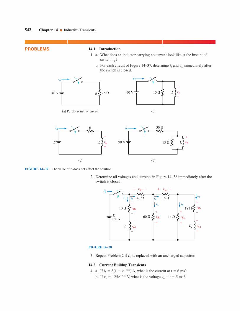
14.1 Introduction
1. a. What does an inductor carrying no current look like at the instant ofswitching?
b. For each circuit of Figure 14–37, determine iS and vL immediately afterthe switch is closed.
542 Chapter 14 Inductive Transients
PROBLEMS
(a) Purely resistive circuit
25 R40 V
iS
(b)
(c) (d)
10 L60 V
iS
vL
LE
iS
vL
R
L
vL90 V
iS 30
15
FIGURE 14–37 The value of L does not affect the solution.
2. Determine all voltages and currents in Figure 14–38 immediately after theswitch is closed.
14 60
40 16
vR3
10 18
E180 V
L1 L2
+
−vR5
+
−
vR6
+
−
vL2
+
−
vR1
vR2 vR4
+
+
−
− + −
vL1
+
−
iT
i1 i2 i4
i3 i5
i6
FIGURE 14–38
3. Repeat Problem 2 if L1 is replaced with an uncharged capacitor.
14.2 Current Buildup Transients
4. a. If iL 8(1 e500t) A, what is the current at t 6 ms?
b. If vL 125e500t V, what is the voltage vL at t 5 ms?

Problems 543
5. The switch of Figure 14–39 is closed at t 0 s.
a. What is the time constant of the circuit?
b. How long is it until current reaches its steady value?
c. Determine the equations for iL and vL.
d. Compute values for iL and vL at intervals of one time constant from t 0to 5 t.
e. Sketch iL and vL. Label the axis in t and in seconds.
6. Close the switch at t 0 s and determine equations for iL and vL for the cir-cuit of Figure 14–40. Compute iL and vL at t 1.8 ms.
7. Repeat Problem 5 for the circuit of Figure 14–41 with L 4 H.
R = 60
iLE 180 V
L = 3 H
vL
FIGURE 14–39
600 mH
vL
t = 0 s
18 V
iL
390
FIGURE 14–40
20 V4
R2
L
16
E
vL
iL
R1
t = 0s
FIGURE 14–41
8. For the circuit of Figure 14–39, determine inductor voltage and current att 50 ms using the universal time constant curve of Figure 14–10.
9. Close the switch at t 0 s and determine equations for iL and vL for the cir-cuit of Figure 14–42. Compute iL and vL at t 3.4 ms.
10. Using Figure 14–10, find vL at one time constant for the circuit of Figure14–42.
11. For the circuit of Figure 14–1(b), the voltage across the inductance at theinstant the switch is closed is 80 V, the final steady state current is 4 A, andthe transient lasts 0.5 s. Determine E, R, and L.
12. For an RL circuit, iL 20(1 et/t) mA and vL 40et/t V. If the transientlasts 0.625 ms, what are E, R, and L?
13. For Figure 14–1(b), if vL 40e2000t V and the steady state current is10 mA, what are E, R, and L?
14.4 De-energizing Transients
14. For Figure 14–43, E 80 V, R1 200 , R2 300 , and L 0.5 H.
a. When the switch is closed, how long does it take for iL to reach steadystate?
b. When the switch is opened, how long does it take for iL to reach steadystate?
c. After the circuit has reached steady state with the switch closed, it isopened. Determine equations for iL and vL.
15. For Figure 14–43, R1 20 , R2 230 , and L 0.5 H, and the inductorcurrent has reached a steady value of 5 A with the switch closed. At t 0 s,the switch is opened.
a. What is the decay time constant?
560 mH
vL
t = 0 s40 V
iL
220
FIGURE 14–42
R2
R1
E iL
L
vL
FIGURE 14–43

b. Determine equations for iL and vL.
c. Compute values for iL and vL at intervals of one time constant from t 0to 5 t.
d. Sketch iL and vL. Label the axis in t and in seconds.
16. Using the values from Problem 15, determine inductor voltage and currentat t 3t using the universal time constant curves shown in Figure 14–10.
17. Given vL 2700 Ve100t. Using the universal time constant curve, find vL
at t 20 ms.
18. For Figure 14–43, the inductor voltage at the instant the switch is closed is150 V and iL 0 A. After the circuit has reached steady state, the switchis opened. At the instant the switch is opened, iL 3 A and vL jumps to750 V. The decay transient lasts 5 ms. Determine E, R1, R2, and L.
19. For Figure 14–43, L 20 H. The current during buildup and decay isshown in Figure 14–44. Determine R1 and R2.
20. For Figure 14–43, when the switch is moved to energization, iL 2 A(1 e10t). Now open the switch after the circuit has reached steady stateand redefine t 0 s as the instant the switch is opened. For this case, vL 400 Ve25t. Determine E, R1, R2, and L.
14.5 More Complex Circuits
21. For the coil of Figure 14–45 R 1.7 and L 150 mH. Determine coilcurrent at t 18.4 ms.
544 Chapter 14 Inductive Transients
iL (A)
t (s)
5 s 2 s
FIGURE 14–44
vL
t = 0 s
67 V
iL 3.9
5.6
4.7
Coil
Rl
L
FIGURE 14–45
22. Refer to Figure 14–46:
a. What is the energizing circuit time constant?
b. Close the switch and determine the equation for iL and vL during currentbuildup.
c. What is the voltage across the inductor and the current through it at t 20 ms?
23. For Figure 14–46, the circuit has reached steady state with the switchclosed. Now open the switch.
a. Determine the de-energizing circuit time constant.
b. Determine the equations for iL and vL.
c. Find the voltage across the inductor and current through it at t 17.8 msusing the equations determined above.
10.5 k
30 k
10 k
iLvL
120 V
L = 0.36 H
FIGURE 14–46

24. Repeat Part (c) of Problem 23 using the universal time constant curvesshown in Figure 14–10.
25. a. Repeat Problem 22, Parts (a) and (b) for the circuit of Figure 14–47.
b. What are iL and vL at t 25 ms?
Problems 545
0.5 A 40 V
200
300
4 H
280
vL
iL
FIGURE 14–47
26. Repeat Problem 23 for the circuit of Figure 14–47, except find vL and iL att 13.8 ms.
27. An unknown circuit containing dc sources and resistors has an open-circuitvoltage of 45 volts. When its output terminals are shorted, the short-circuitcurrent is 0.15 A. A switch, resistor, and inductance are connected (Figure14–48). Determine the inductor current and voltage 2.5 ms after the switchis closed.
28. The circuit of Figure 14–49 is in steady state with the switch in position 1.At t 0, it is moved to position 2, where it remains for 1.0 s. It is thenmoved to position 3, where it remains. Sketch curves for iL and vL from t 0
until the circuit reaches steady state in position 3. Compute the inductorvoltage and current at t 0.1 s and at t 1.1 s.
100
L = 0.4 H
iL
Unk
now
nci
rcui
t
vL
FIGURE 14–48
15
3
50
30
12
25 V
5 H
vL
iL
FIGURE 14–49
14.6 RL Transients Using Computers
29. EWB or PSpice The switch of Figure 14–46 is closed at t 0 andremains closed. Graph the voltage across L and find vL at 20 ms using thecursor.
30. EWB or PSpice For the circuit of Figure 14–47, close the switch at t 0and find vL at t 10 ms. (For PSpice, use current source IDC.)

31. EWB or PSpice For Figure 14–6, let L1 30 mH and L2 90 mH.Close the switch at t 0 and find the current in the 30 resistor at t 2 ms.(Answer: 4.61 A) [Hint for Workbench users: Redraw the circuit with L1 andthe 30 resistor interchanged. Finally, use Ohm’s law.]
32. EWB or PSpice For Figure 14–41, let L 4 H. Solve for vL and, usingthe cursor, measure values at t 200 ms and 500 ms. For PSpice users, alsofind current at these times.
33. PSpice We solved the circuit of Figure 14–21(a) by reducing it to itsThévenin equivalent. Using PSpice, analyze the circuit in its original formand plot the inductor current. Check a few points on the curve by computingvalues according to the solution of Example 14–8 and compare to valuesobtained from screen.
34. PSpice The circuit of Figure 14–46 is in steady state with the switchopen. At t 0, the switch is closed. It remains closed for 150 ms and is thenopened and left open. Compute and plot iL and vL. With the cursor, deter-mine values at t 60 ms and at t 165 ms.
546 Chapter 14 Inductive Transients
In-Process Learning Check 1
1. a. 20e100 000t V; 2(1 e100 000t) mA
b.
ANSWERS TO IN-PROCESSLEARNING CHECKS
t(s) vL (V) iL (mA)
0 20 010 7.36 1.2620 2.71 1.7330 0.996 1.9040 0.366 1.9650 0.135 1.99
c.
20 V
t
vss = 0 V
5 = 50 µs
i
iss = 2 mA
vL
2. 11.5 V; 1.47 A
3. 4 V
4. 3.88 A


OBJECTIVES
After studying this chapter, you will beable to
• explain how ac voltages and currentsdiffer from dc,
• draw waveforms for ac voltage and cur-rents and explain what they mean,
• explain the voltage polarity and currentdirection conventions used for ac,
• describe the basic ac generator andexplain how ac voltage is generated,
• define and compute frequency, period,amplitude, and peak-to-peak values,
• compute instantaneous sinusoidal volt-age or current at any instant in time,
• define the relationships between q, T,and f for a sine wave,
• define and compute phase differencesbetween waveforms,
• use phasors to represent sinusoidal volt-ages and currents,
• determine phase relationships betweenwaveforms using phasors,
• define and compute average values fortime-varying waveforms,
• define and compute effective values fortime-varying waveforms,
• use Electronics Workbench and PSpiceto study ac waveforms.
KEY TERMS
ac
Alternating Voltage
Alternating Current
Amplitude
Angular Velocity
Average Value
Cycle
Effective Value
Frequency
Hertz
Instantaneous Value
Oscilloscope
Peak Value
Period
Phase Shifts
Phasor
RMS
Sine Wave
OUTLINE
Introduction
Generating AC Voltages
Voltage and Current Conventions for AC
Frequency, Period, Amplitude, and PeakValue
Angular and Graphic Relationships forSine Waves
Voltage and Currents as Functions of Time
Introduction to Phasors
AC Waveforms and Average Value
Effective Values
Rate of Change of a Sine Wave
AC Voltage and Current Measurement
Circuit Analysis Using Computers
AC Fundamentals15

Alternating currents (ac) are currents that alternate in direction (usuallymany times per second), passing first in one direction, then in the other
through a circuit. Such currents are produced by voltage sources whose polari-ties alternate between positive and negative (rather than being fixed as with dcsources). By convention, alternating currents are called ac currents and alternat-ing voltages are called ac voltages.
The variation of an ac voltage or current versus time is called its waveform.Since waveforms vary with time, they are designated by lowercase letters v(t),i(t), e(t), and so on, rather than by uppercase letters V, I, and E as for dc. Oftenwe drop the functional notation and simply use v, i, and e.
While many waveforms are important to us, the most fundamental is thesine wave (also called sinusoidal ac). In fact, the sine wave is of such importancethat many people associate the term ac with sinusoidal, even though ac refers toany quantity that alternates with time.
In this chapter, we look at basic ac principles, including the generation of acvoltages and ways to represent and manipulate ac quantities. These ideas arethen used throughout the remainder of the book to develop methods of analysisfor ac circuits.
549
CHAPTER PREVIEW
PUTTING IT INPERSPECTIVE
Thomas Alva Edison
NOWADAYS WE TAKE IT FOR GRANTED that our electrical power systems are ac.(This is driven home every time you see a piece of equipment rated “60 hertzac”, for example.) However, this was not always the case. In the late 1800s, afierce battle—the so-called “war of the currents”—raged in the emerging electri-cal power industry. The forces favoring the use of dc were led by Thomas AlvaEdison, and those favoring the use of ac were led by George Westinghouse(Chapter 24) and Nikola Tesla (Chapter 23).
Edison, a prolific inventor who gave us the electric light, the phonograph,and many other great inventions as well, fought vigorously for dc. He had spenta considerable amount of time and money on the development of dc power andhad a lot at stake, in terms of both money and prestige. So unscrupulous wasEdison in this battle that he first persuaded the state of New York to adopt ac forits newly devised electric chair, and then pointed at it with horror as an exampleof how deadly ac was. Ultimately, however, the combination of ac’s advantagesover dc and the stout opposition of Tesla and Westinghouse won the day for ac.
Edison was born in 1847 in Milan, Ohio. Most of his work was done at twosites in New Jersey—first at a laboratory in Menlo Park, and later at a muchlarger laboratory in West Orange, where his staff at one time numbered around5,000. He received patents as inventor or co-inventor on an astonishing 1,093inventions, making him probably the greatest inventor of all time.
Thomas Edison died at the age of 84 on October 18, 1831.

15.1 IntroductionPreviously you learned that dc sources have fixed polarities and constantmagnitudes and thus produce currents with constant value and unchangingdirection, as illustrated in Figure 15–1. In contrast, the voltages of ac sourcesalternate in polarity and vary in magnitude and thus produce currents thatvary in magnitude and alternate in direction.
550 Chapter 15 AC Fundamentals
(a)
I = 2 A
E 12 V 12 V
6 t0
12 V
Vol
tage
or
Cur
rent
2 A
(b) Voltage and currentversus time for dc
FIGURE 15–1 In a dc circuit, voltage polarities and current directions do not change.
Sinusoidal AC VoltageTo illustrate, consider the voltage at the wall outlet in your home. Called asine wave or sinusoidal ac waveform (for reasons discussed in Section15.5), this voltage has the shape shown in Figure 15–2. Starting at zero, thevoltage increases to a positive maximum, decreases to zero, changes polarity,increases to a negative maximum, then returns again to zero. One completevariation is referred to as a cycle. Since the waveform repeats itself at regularintervals as in (b), it is called a periodic waveform.
Vol
tage
t0
Voltage is positive
Voltage isnegative
Polaritychange
1 cycle
(a) Variation of voltageversus time
Vol
tage
t
(b) A continuous streamof cycles
FIGURE 15–2 Sinusoidal ac waveforms. Values above the axis are positive while val-ues below are negative.
Symbol for an AC Voltage SourceThe symbol for a sinusoidal voltage source is shown in Figure 15–3. Notethat a lowercase e is used to represent voltage rather than E, since it is afunction of time. Polarity marks are also shown although, since the polarityof the source varies, their meaning has yet to be established.
e(t)
FIGURE 15–3 Symbol for a sinu-soidal voltage source. Lowercase lettere is used to indicate that the voltagevaries with time.

Sinusoidal AC CurrentFigure 15–4 shows a resistor connected to an ac source. During the first half-cycle, the source voltage is positive; therefore, the current is in the clockwisedirection. During the second half-cycle, the voltage polarity reverses; there-fore, the current is in the counterclockwise direction. Since current is propor-tional to voltage, its shape is also sinusoidal (Figure 15–5).
Section 15.2 Generating AC Voltages 551
R
Actual current directionduring first half-cycle
Actualsource
polarityduringfirst
half-cycle
(a)
R
Actual current directionduring second half-cycle
Actualsource
polarityduringsecond
half-cycle
(b)
FIGURE 15–4 Current direction reverses when the source polarity reverses.
t0
VoltageCurrent
FIGURE 15–5 Current has the samewave shape as voltage.
15.2 Generating AC VoltagesOne way to generate an ac voltage is to rotate a coil of wire at constantangular velocity in a fixed magnetic field, Figure 15–6. (Slip rings andbrushes connect the coil to the load.) The magnitude of the resulting voltageis proportional to the rate at which flux lines are cut (Faraday’s law, Chapter13), and its polarity is dependent on the direction the coil sides movethrough the field. Since the rate of cutting flux varies with time, the resultingvoltage will also vary with time. For example in (a), since the coil sides aremoving parallel to the field, no flux lines are being cut and the induced volt-age at this instant (and hence the current) is zero. (This is defined as the 0°position of the coil.) As the coil rotates from the 0° position, coil sides AAand BB cut across flux lines; hence, voltage builds, reaching a peak whenflux is cut at the maximum rate in the 90° position as in (b). Note the polar-ity of the voltage and the direction of current. As the coil rotates further,voltage decreases, reaching zero at the 180° position when the coil sidesagain move parallel to the field as in (c). At this point, the coil has gonethrough a half-revolution.
During the second half-revolution, coil sides cut flux in directionsopposite to that which they did in the first half revolution; hence, thepolarity of the induced voltage reverses. As indicated in (d), voltagereaches a peak at the 270° point, and, since the polarity of the voltage haschanged, so has the direction of current. When the coil reaches the 360°position, voltage is again zero and the cycle starts over. Figure 15–7shows one cycle of the resulting waveform. Since the coil rotates continu-ously, the voltage produced will be a repetitive, periodic waveform as yousaw in Figure 15–2(b).
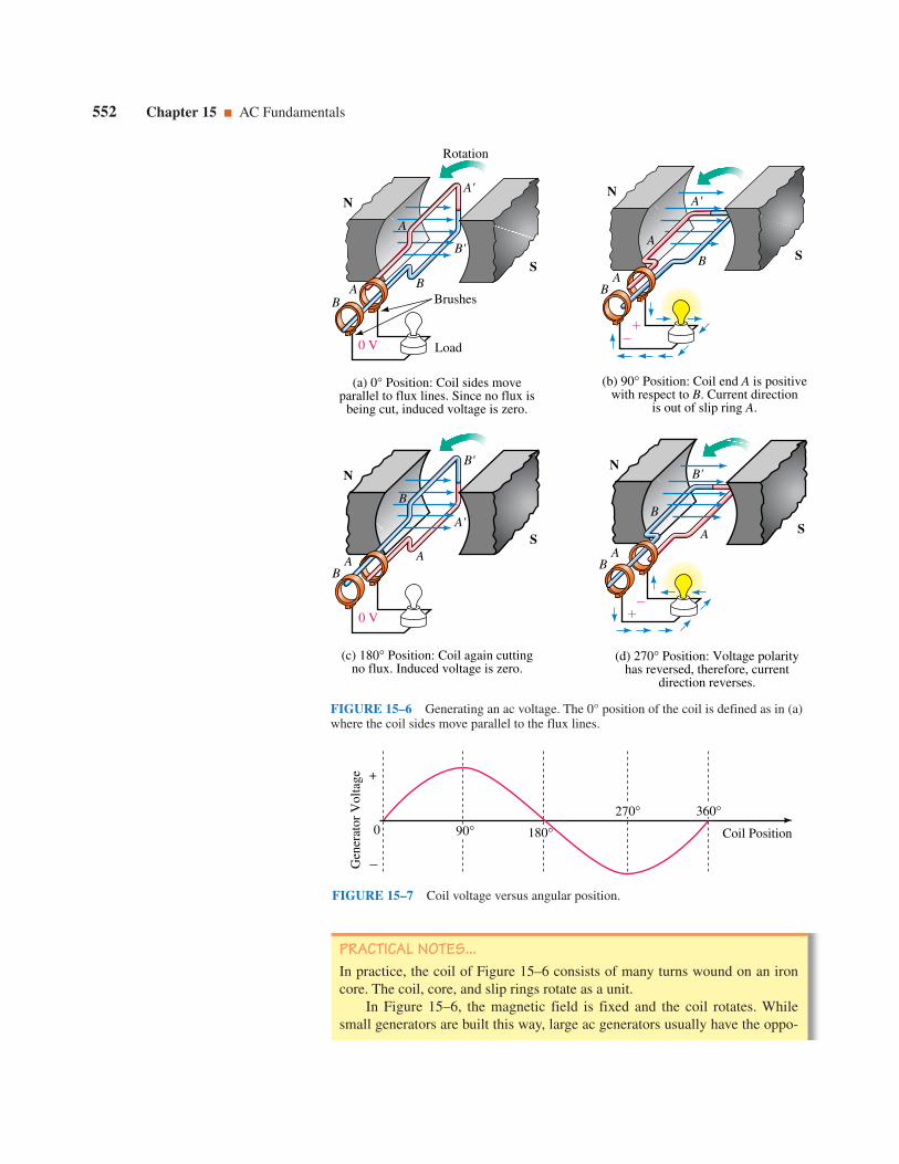
552 Chapter 15 AC Fundamentals
B'
B
BA
A
A'
Load
Brushes
Rotation
0 V
N
S
(a) 0° Position: Coil sides moveparallel to flux lines. Since no flux is
being cut, induced voltage is zero.
A
A
A'N
(b) 90° Position: Coil end A is positivewith respect to B. Current direction
is out of slip ring A.
B
B
S
A
B
B'
A'
0 V
N
S
(c) 180° Position: Coil again cuttingno flux. Induced voltage is zero.
AB
B
B'N
(d) 270° Position: Voltage polarityhas reversed, therefore, current
direction reverses.
A S
AB
FIGURE 15–6 Generating an ac voltage. The 0° position of the coil is defined as in (a)where the coil sides move parallel to the flux lines.
FIGURE 15–7 Coil voltage versus angular position.
0
Gen
erat
or V
olta
ge
90° 180°
270° 360°
+
Coil Position
PRACTICAL NOTES...In practice, the coil of Figure 15–6 consists of many turns wound on an ironcore. The coil, core, and slip rings rotate as a unit.
In Figure 15–6, the magnetic field is fixed and the coil rotates. Whilesmall generators are built this way, large ac generators usually have the oppo-

Time ScalesThe horizontal axis of Figure 15–7 is scaled in degrees. Often we need itscaled in time. The length of time required to generate one cycle depends onthe velocity of rotation. To illustrate, assume that the coil rotates at 600 rpm(revolutions per minute). Six hundred revolutions in one minute equals 600rev/60 s 10 revolutions in one second. At ten revolutions per second, thetime for one revolution is one tenth of a second, i.e., 100 ms. Since one cycleis 100 ms, a half-cycle is 50 ms, a quarter-cycle is 25 ms, and so on. Figure15–8 shows the waveform rescaled in time.
Instantaneous ValueAs Figure 15–8 shows, the coil voltage changes from instant to instant. Thevalue of voltage at any point on the waveform is referred to as its instanta-neous value. This is illustrated in Figure 15–9. Figure 15–9(a) shows a pho-tograph of an actual waveform, and (b) shows it redrawn, with values scaledfrom the photo. For this example, the voltage has a peak value of 40 voltsand a cycle time of 6 ms. From the graph, we see that at t 0 ms, the volt-age is zero. At t 0.5 ms, it is 20 V. At t 2 ms, it is 35 V. At t 3.5 ms, itis 20 V, and so on.
Section 15.2 Generating AC Voltages 553
t (ms)0 25 50 75 100
e(t)
Cycle
Half-cycle point
Gen
erat
or V
olta
ge
FIGURE 15–8 Cycle scaled in time.At 600 rpm, the cycle length is 100 ms.
site construction, that is, their coils are fixed and the magnetic field is rotatedinstead. In addition, large ac generators are usually made as three-phasemachines with three sets of coils instead of one. This is covered in Chapter23. However, although its details are oversimplified, the generator of Figure15–6 gives a true picture of the voltage produced by a real ac generator.
(a) Sinusoidal voltage
FIGURE 15–9 Instantaneous values.
e (V)
1
100
30
102030
20
2 4 5 6t (ms)
40
40
3
28 V
35 V
20 V
20 V
(b) Values scaled from the photograph

Electronic Signal GeneratorsAC waveforms may also be created electronically using signal generators. Infact, with signal generators, you are not limited to sinusoidal ac. The gen-eral-purpose lab signal generator of Figure 15–10, for example, can producea variety of variable-frequency waveforms, including sinusoidal, squarewave, triangular, and so on. Waveforms such as these are commonly used totest electronic gear.
554 Chapter 15 AC Fundamentals
Square wave
t
Triangle wave
t
Sine wave
t
(b) Sample waveforms
(a) A typical signal generator
FIGURE 15–10 Electronic signal generators produce waveforms of different shapes.
15.3 Voltage and Current Conventions for ACIn Section 15.1, we looked briefly at voltage polarities and current directions.At that time, we used separate diagrams for each half-cycle (Figure 15–4).However, this is unnecessary; one diagram and one set of references is all that isrequired. This is illustrated in Figure 15–11. First, we assign reference polari-ties for the source and a reference direction for the current. We then use the con-vention that, when e has a positive value, its actual polarity is the same as thereference polarity, and when e has a negative value, its actual polarity is oppo-site to that of the reference. For current, we use the convention that when i has apositive value, its actual direction is the same as the reference arrow, and when ihas a negative value, its actual direction is opposite to that of the reference.

Section 15.3 Voltage and Current Conventions for AC 555
R
(a) References for voltageand current.
e
i
t
i
e
(b) During the first half-cycle,voltage polarity and current
direction are as shown in (a).Therefore, e and i are positive.During the second half-cycle,voltage polarity and currentdirection are opposite to that
shown in (a). Therefore, e and i are negative.
FIGURE 15–11 AC voltage and current reference conventions.
To illustrate, consider Figure 15–12. At time t1, e has a value of 10 volts.This means that at this instant, the voltage of the source is 10 V and its topend is positive with respect to its bottom end. This is indicated in (b). With avoltage of 10 V and a resistance of 5 , the instantaneous value of current isi e/R 10 V/5 2 A. Since i is positive, the current is in the directionof the reference arrow.
tt1
t2
()
()
i
e10 V
10 V
2 A
2 A
(a)
5
(b) Time t1: e = 10 V andi = 2 A. Thus voltage andcurrent have the polarityand direction indicated
e
i = 2 A
5
(c) Time t2: e = 10 V and i = 2 A.Thus, voltage polarity is opposite tothat indicated and current direction is opposite to the arrow direction.
e
i = 2 A
FIGURE 15–12 Illustrating the ac voltage and current convention.
Now consider time t2. Here, e 10 V. This means that source voltageis again 10 V, but now its top end is negative with respect to its bottom end.Again applying Ohm’s law, you get i e/R 10 V/5 2 A. Since iis negative, current is actually opposite in direction to the reference arrow.This is indicated in (c).
The above concept is valid for any ac signal, regardless of waveshape.
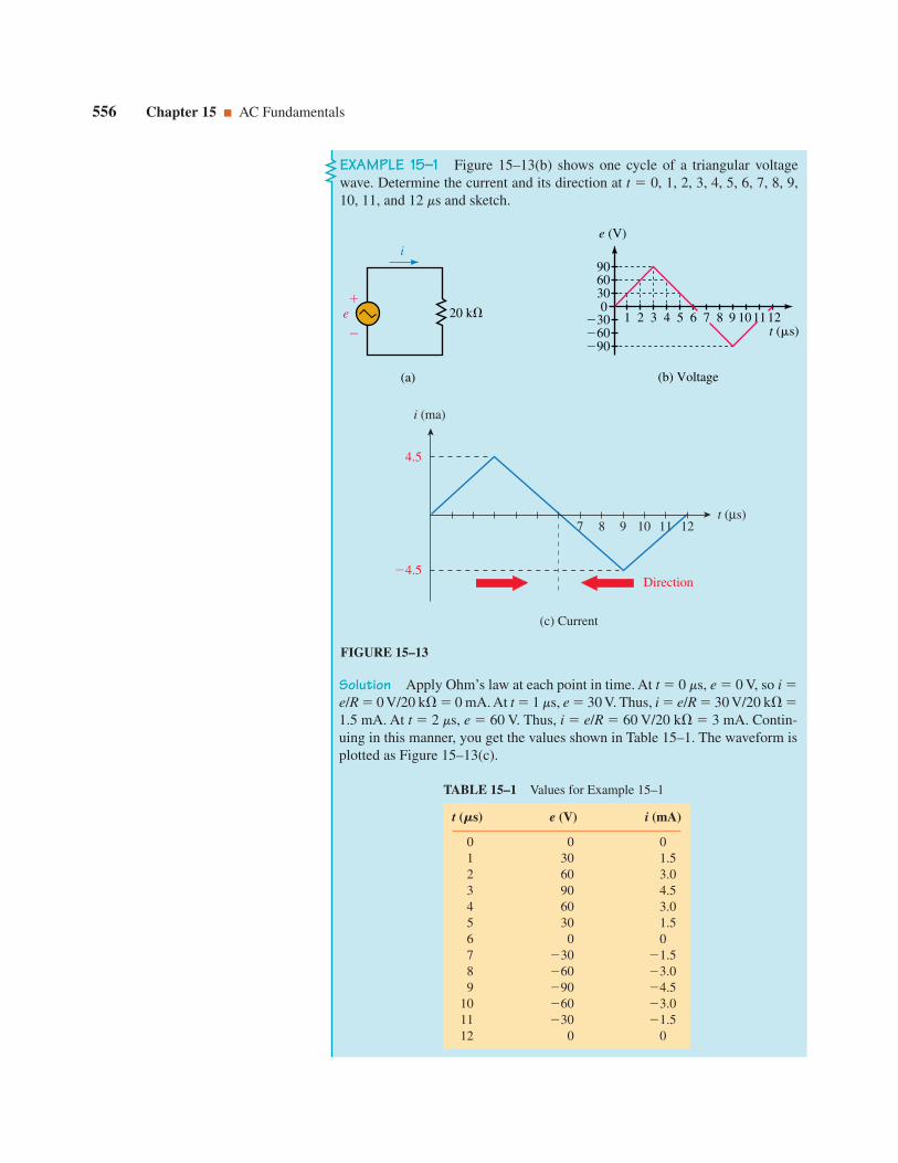
556 Chapter 15 AC Fundamentals
EXAMPLE 15–1 Figure 15–13(b) shows one cycle of a triangular voltagewave. Determine the current and its direction at t 0, 1, 2, 3, 4, 5, 6, 7, 8, 9,10, 11, and 12 ms and sketch.
TABLE 15–1 Values for Example 15–1
t (s) e (V) i (mA)
0 0 01 30 1.52 60 3.03 90 4.54 60 3.05 30 1.56 0 07 30 1.58 60 3.09 90 4.5
10 60 3.011 30 1.512 0 0
Solution Apply Ohm’s law at each point in time. At t 0 ms, e 0 V, so i e/R 0 V/20 k 0 mA. At t 1 ms, e 30 V. Thus, i e/R 30 V/20 k 1.5 mA. At t 2 ms, e 60 V. Thus, i e/R 60 V/20 k 3 mA. Contin-uing in this manner, you get the values shown in Table 15–1. The waveform isplotted as Figure 15–13(c).
20 k
(a)
e
i
(b) Voltage
e (V)
1 20
90
90
3 4t (s)
6030
6030 5 7 8 9 1011126
11
4.5
4.5
7 8 9 10 12
Direction
i (ma)
t (µs)
(c) Current
FIGURE 15–13
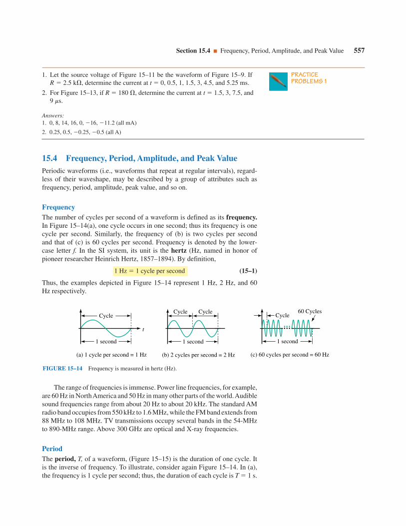
15.4 Frequency, Period, Amplitude, and Peak ValuePeriodic waveforms (i.e., waveforms that repeat at regular intervals), regard-less of their waveshape, may be described by a group of attributes such asfrequency, period, amplitude, peak value, and so on.
FrequencyThe number of cycles per second of a waveform is defined as its frequency.In Figure 15–14(a), one cycle occurs in one second; thus its frequency is onecycle per second. Similarly, the frequency of (b) is two cycles per secondand that of (c) is 60 cycles per second. Frequency is denoted by the lower-case letter f. In the SI system, its unit is the hertz (Hz, named in honor ofpioneer researcher Heinrich Hertz, 1857–1894). By definition,
1 Hz 1 cycle per second (15–1)
Thus, the examples depicted in Figure 15–14 represent 1 Hz, 2 Hz, and 60Hz respectively.
Section 15.4 Frequency, Period, Amplitude, and Peak Value 557
PRACTICEPROBLEMS 1
1. Let the source voltage of Figure 15–11 be the waveform of Figure 15–9. IfR 2.5 k, determine the current at t 0, 0.5, 1, 1.5, 3, 4.5, and 5.25 ms.
2. For Figure 15–13, if R 180 , determine the current at t 1.5, 3, 7.5, and9 ms.
Answers:1. 0, 8, 14, 16, 0, 16, 11.2 (all mA)
2. 0.25, 0.5, 0.25, 0.5 (all A)
1 second
Cycle Cycle
1 second
Cycle60 Cycles
t
1 second
Cycle
• • •• • •
(a) 1 cycle per second = 1 Hz (b) 2 cycles per second = 2 Hz (c) 60 cycles per second = 60 Hz
FIGURE 15–14 Frequency is measured in hertz (Hz).
The range of frequencies is immense. Power line frequencies, for example,are 60 Hz in NorthAmerica and 50 Hz in many other parts of the world.Audiblesound frequencies range from about 20 Hz to about 20 kHz. The standard AMradio band occupies from 550 kHz to 1.6 MHz, while the FM band extends from88 MHz to 108 MHz. TV transmissions occupy several bands in the 54-MHzto 890-MHz range. Above 300 GHz are optical and X-ray frequencies.
PeriodThe period, T, of a waveform, (Figure 15–15) is the duration of one cycle. Itis the inverse of frequency. To illustrate, consider again Figure 15–14. In (a),the frequency is 1 cycle per second; thus, the duration of each cycle is T 1 s.
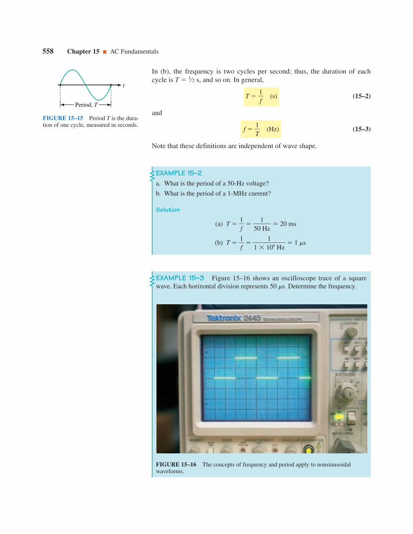
In (b), the frequency is two cycles per second; thus, the duration of eachcycle is T 1⁄2 s, and so on. In general,
T 1f (s) (15–2)
and
f T1
(Hz) (15–3)
Note that these definitions are independent of wave shape.
558 Chapter 15 AC Fundamentals
t
Period, T
FIGURE 15–15 Period T is the dura-tion of one cycle, measured in seconds.
EXAMPLE 15–2a. What is the period of a 50-Hz voltage?
b. What is the period of a 1-MHz current?
Solution
(a) T 1f
501Hz 20 ms
(b) T 1f
1 1106 Hz 1 ms
EXAMPLE 15–3 Figure 15–16 shows an oscilloscope trace of a squarewave. Each horizontal division represents 50 ms. Determine the frequency.
FIGURE 15–16 The concepts of frequency and period apply to nonsinusoidalwaveforms.
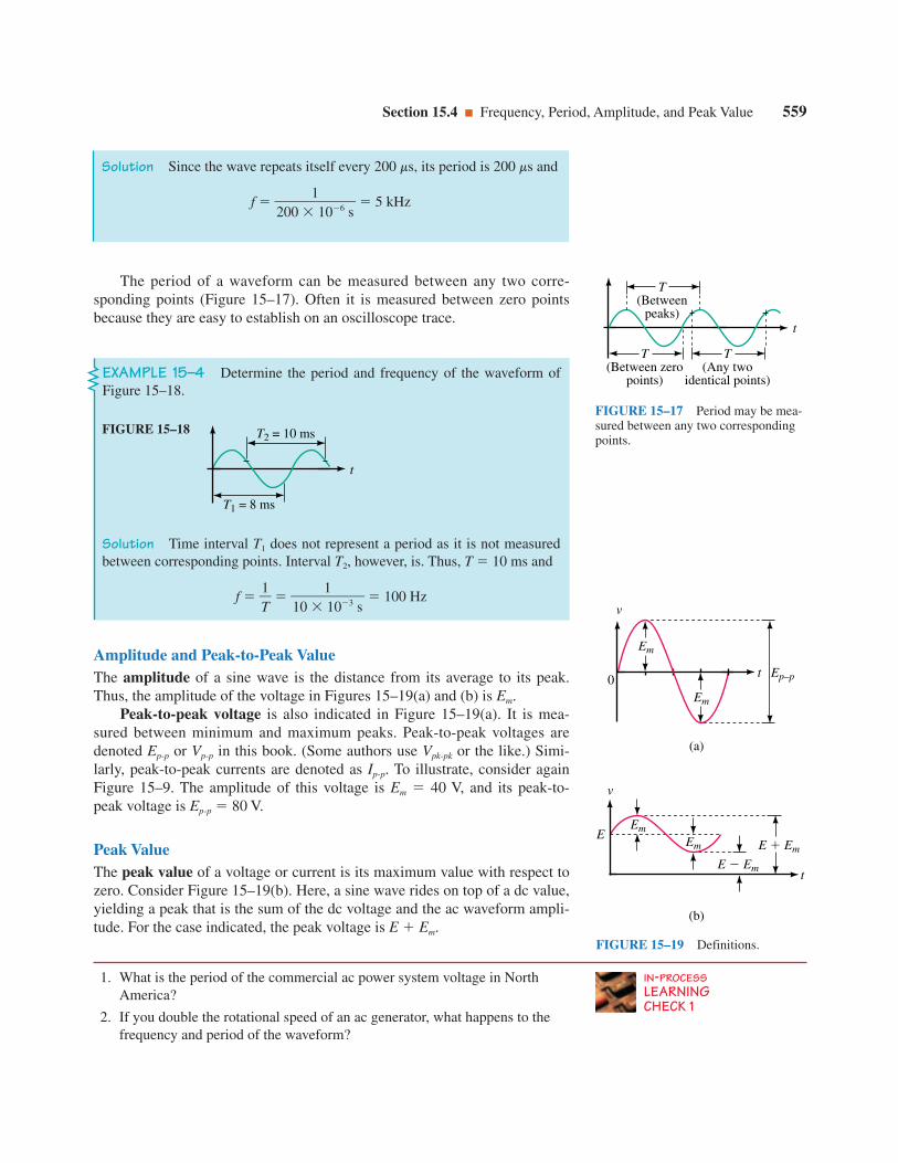
The period of a waveform can be measured between any two corre-sponding points (Figure 15–17). Often it is measured between zero pointsbecause they are easy to establish on an oscilloscope trace.
Section 15.4 Frequency, Period, Amplitude, and Peak Value 559
Solution Since the wave repeats itself every 200 ms, its period is 200 ms and
f 200
1106 s 5 kHz
t
T(Between
peaks)
T(Between zero
points)
T(Any two
identical points)
FIGURE 15–17 Period may be mea-sured between any two correspondingpoints.
EXAMPLE 15–4 Determine the period and frequency of the waveform ofFigure 15–18.
Solution Time interval T1 does not represent a period as it is not measuredbetween corresponding points. Interval T2, however, is. Thus, T 10 ms and
f T1
10
1103 s 100 Hz
FIGURE 15–18
t
T2 = 10 ms
T1 = 8 ms
Amplitude and Peak-to-Peak ValueThe amplitude of a sine wave is the distance from its average to its peak.Thus, the amplitude of the voltage in Figures 15–19(a) and (b) is Em.
Peak-to-peak voltage is also indicated in Figure 15–19(a). It is mea-sured between minimum and maximum peaks. Peak-to-peak voltages aredenoted Ep-p or Vp-p in this book. (Some authors use Vpk-pk or the like.) Simi-larly, peak-to-peak currents are denoted as Ip-p. To illustrate, consider againFigure 15–9. The amplitude of this voltage is Em 40 V, and its peak-to-peak voltage is Ep-p 80 V.
Peak ValueThe peak value of a voltage or current is its maximum value with respect tozero. Consider Figure 15–19(b). Here, a sine wave rides on top of a dc value,yielding a peak that is the sum of the dc voltage and the ac waveform ampli-tude. For the case indicated, the peak voltage is E Em.
t
v
EEm
(b)
t0
v
Em
Ep–p
E Em
E Em
Em
(a)
Em
FIGURE 15–19 Definitions.
IN-PROCESSLEARNINGCHECK 1
1. What is the period of the commercial ac power system voltage in NorthAmerica?
2. If you double the rotational speed of an ac generator, what happens to thefrequency and period of the waveform?

3. If the generator of Figure 15–6 rotates at 3000 rpm, what is the period andfrequency of the resulting voltage? Sketch four cycles and scale the horizon-tal axis in units of time.
4. For the waveform of Figure 15–9, list all values of time at which e 20 Vand e 35 V. Hint: Sine waves are symmetrical.
5. Which of the waveform pairs of Figure 15–20 are valid combinations?Why?
560 Chapter 15 AC Fundamentals
i
e
(a) Circuit
i
(b)
e
i
(c)
e
i
(d)
e
FIGURE 15–20 Which waveform pairs are valid?
6. For the waveform in Figure 15–21, determine the frequency.
v
1 20
3
213
t (ms)3 4 7 8 9 1011125 6
FIGURE 15–21
7. Two waveforms have periods of T1 10 ms and T2 30 ms respectively.Which has the higher frequency? Compute the frequencies of both wave-forms.
8. Two sources have frequencies f1 and f2 respectively. If f2 20f1, and T2 is1 ms, what is f1? What is f2?
9. Consider Figure 15–22. What is the frequency of the waveform?
FIGURE 15–22
t
100 ms
i
10. For Figure 15–11, if f 20 Hz, what is the current direction at t 12 ms,37 ms, and 60 ms? Hint: Sketch the waveform and scale the horizontal axisin ms. The answers should be apparent.
11. A 10-Hz sinusoidal current has a value of 5 amps at t 25 ms. What is itsvalue at t 75 ms? See hint in Problem 10.
(Answers are at the end of the chapter.)
Section 15.5 Angular and Graphic Relationships for Sine Waves 561
15.5 Angular and Graphic Relationships for Sine Waves
The Basic Sine Wave EquationConsider again the generator of Figure 15–6, reoriented and redrawn in endview as Figure 15–23. The voltage produced by this generator is
e Emsin a (V) (15–4)
where Em is the maximum coil voltage and a is the instantaneous angularposition of the coil. (For a given generator and rotational velocity, Em is con-stant.) Note that a 0° represents the horizontal position of the coil and thatone complete cycle corresponds to 360°. Equation 15–4 states that the volt-age at any point on the sine wave may be found by multiplying Em times thesine of the angle at that point.
(a) End view showing coil position
N
S
α
Rotation
0°
0
(b) Voltage waveform
90° 180° 270° 360°α
Em
Em
e
Rotatione = Emsin α
FIGURE 15–23 Coil voltage versusangular position.
EXAMPLE 15–5 If the amplitude of the waveform of Figure 15–23(b) isEm 100 V, determine the coil voltage at 30° and 330°.
Solution At a 30°, e Em sin a 100 sin 30° 50 V. At 330°, e 100sin 330° 50 V. These are shown on the graph of Figure 15–24.
FIGURE 15–24
e (V)
0 α
100
100
50 V
30°330°
50 V
PRACTICEPROBLEMS 2
Table 15–2 is a tabulation of voltage versus angle computed from e 100 sin a.Use your calculator to verify each value, then plot the result on graph paper. Theresulting waveshape should look like Figure 15–24.

Angular Velocity,
The rate at which the generator coil rotates is called its angular velocity. If thecoil rotates through an angle of 30° in one second, for example, its angularvelocity is 30° per second. Angular velocity is denoted by the Greek letter q
(omega). For the case cited, q 30°/s. (Normally angular velocity is expressedin radians per second instead of degrees per second. We will make this changeshortly.) When you know the angular velocity of a coil and the length of timethat it has rotated, you can compute the angle through which it has turned. Forexample, a coil rotating at 30°/s rotates through an angle of 30° in one second,60° in two seconds, 90° in three seconds, and so on. In general,
a qt (15–5)
Expressions for t and q can now be found. They are
t a
q (s) (15–6)
q a
t (15–7)
562 Chapter 15 AC Fundamentals
TABLE 15–2 Data for Plotting e 100 sin a
Angle Voltage e
0 030 5060 86.690 100
120 86.6150 50180 0210 50240 86.6270 100300 86.6330 50360 0
EXAMPLE 15–6 If the coil of Figure 15–23 rotates at q 300°/s, howlong does it take to complete one revolution?
Solution One revolution is 360°. Thus,
t a
q 1.2 s
Since this is one period, we should use the symbol T. Thus, T 1.2 s, as inFigure 15–25.
360 degrees
300deg
s
rees
Radian MeasureIn practice, q is usually expressed in radians per second, where radians anddegrees are related by the identity
2p radians 360° (15–8)
One radian therefore equals 360°/2p 57.296°. A full circle, as shown inFigure 15–26(a), can be designated as either 360° or 2p radians. Likewise,the cycle length of a sinusoid, shown in Figure 15–26(b), can be stated aseither 360° or 2p radians; a half-cycle as 180° or p radians, and so on.
To convert from degrees to radians, multiply by p/180, while to convertfrom radians to degrees, multiply by 180/p.
aradians 18p
0° adegrees (15–9)
adegrees 18p
0° aradians (15–10)
Table 15–3 shows selected angles in both measures.
Section 15.5 Angular and Graphic Relationships for Sine Waves 563
FIGURE 15–25
t0
e
T = 1.2 s
PRACTICEPROBLEMS 3
If the coil of Figure 15–23 rotates at 3600 rpm, determine its angular velocity, q,in degrees per second.
Answer: 21 600 deg/s
0
(b) Cycle length scaled in degrees and radians
(a) 360° = 2 radians
90°0 180° 270° 360°
/2 23/2 (radians)
(degrees)
°360°o
r2
radi
ans
FIGURE 15–26 Radian measure.
TABLE 15–3 Selected Angles in Degrees and Radians
Degrees Radians
30 p/645 p/460 p/390 p/2
180 p
270 3p/2360 2p
EXAMPLE 15–7a. Convert 315° to radians.
b. Convert 5p/4 radians to degrees.

Scientific calculators can perform these conversions directly. You willfind this more convenient than using the above formulas.
Graphing Sine WavesA sinusoidal waveform can be graphed with its horizontal axis scaled indegrees, radians, or time. When scaled in degrees or radians, one cycle isalways 360° or 2p radians (Figure 15–27); when scaled in time, it is fre-quency dependent, since the length of a cycle depends on the coil’s velocityof rotation. However, if scaled in terms of period T instead of in seconds, thewaveform is also frequency independent, since one cycle is always T, asshown in Figure 15–27(c).
When graphing a sine wave, you don’t actually need many points to geta good sketch: Values every 45° (one eighth of a cycle) are generally ade-quate. Table 15–4 shows corresponding values for sin a at this spacing.
564 Chapter 15 AC Fundamentals
Solutiona. aradians (p/180°)(315°) 5.5 rad
b. adegrees (180°/p)(5p/4) 225°
(b) Radians
α (°)
360°
0 90 180 270 360
(a) Degrees
α (rad)
2 rad
02 22
3
(c) Period
t
T (s)
04T
2T T4
3T
FIGURE 15–27 Comparison of vari-ous horizontal scales. Cycle length maybe scaled in degrees, radians or period.Each of these is independent of fre-quency.
TABLE 15–4 Values for Rapid Sketching
(deg) (rad) t (T) Value of sin
0 0 0 0.045 p/4 T/8 0.70790 p/2 T/4 1.0
135 3p/4 3T/8 0.707180 p T/2 0.0225 5p/4 5T/8 0.707270 3p/2 3T/4 1.0315 7p/4 7T/8 0.707360 2p T 0.0
EXAMPLE 15–8 Sketch the waveform for a 25-kHz sinusoidal current thathas an amplitude of 4 mA. Scale the axis in seconds.
Solution The easiest approach is to use T 1/f, then scale the graphaccordingly. For this waveform, T 1/25 kHz 40 ms. Thus,
1. Mark the end of the cycle as 40 ms, the half-cycle point as 20 ms, the quarter-cycle point as 10 ms, and so on (Figure 15–28).
2. The peak value (i.e., 4 mA) occurs at the quarter-cycle point, which is 10 mson the waveform. Likewise, 4 mA occurs at 30 ms. Now sketch.
3. Values at other time points can be determined easily. For example, thevalue at 5 ms can be calculated by noting that 5 ms is one eighth of a cycle,or 45°. Thus, i 4 sin 45° mA 2.83 mA. Alternately, from Table 15–4,
15.6 Voltages and Currents as Functions of Time
Relationship between , T, and fEarlier you learned that one cycle of sine wave may be represented as eithera 2p rads or t T s, Figure 15–27. Substituting these into a qt (Equa-tion 15–5), you get 2p qT. Transposing yields
qT 2p (rad) (15–11)
Thus,
q 2Tp (rad/s) (15–12)
Recall, f 1/T Hz. Substituting this into Equation 15–12 you get
q 2pf (rad/s) (15–13)
Section 15.6 Voltages and Currents as Functions of Time 565
at T/8, i (4 mA)(0.707) 2.83 mA. As many points as you need can becomputed and plotted in this manner.
4. Values at particular angles can also be located easily. For instance, if youwant a value at 30°, the required value is i 4 sin 30° mA 2.0 mA.To locate this point, note that 30° is one twelfth of a cycle or T/12 (40 ms)/12 3.33 ms. The point is shown on Figure 15–28.
FIGURE 15–28 i (mA)
1050 t (s)
42.83
2.834
153.33 s
30 3525 4020
i = 2 mA att = 3.33 s— see text
T = 40 s
EXAMPLE 15–9 In some parts of the world, the power system frequency is60 Hz; in other parts, it is 50 Hz. Determine q for each.
Solution For 60 Hz, q 2pf 2p(60) 377 rad/s. For 50 Hz, q 2pf 2p(50) 314.2 rad/s.
PRACTICEPROBLEMS 4
1. If q 240 rad/s, what are T and f? How many cycles occur in 27 s?
2. If 56 000 cycles occur in 3.5 s, what is q?
Answers:1. 26.18 ms, 38.2 Hz, 1031 cycles
2. 100.5 103 rad/s

Sinusoidal Voltages and Currents as Functions of TimeRecall from Equation 15–4, e Em sin a, and from Equation 15–5, a qt.Combining these equations yields
e Emsin qt (15–14a)
Similarly,
v Vmsin qt (15–14b)
i Imsin qt (15–14c)
566 Chapter 15 AC Fundamentals
EXAMPLE 15–10 A 100-Hz sinusoidal voltage source has an amplitude of150 volts. Write the equation for e as a function of time.
Solution q 2pf 2p(100) 628 rad/s and Em 150 V. Thus, e Emsinqt 150 sin 628t V.
Equations 15–14 may be used to compute voltages or currents at anyinstant in time. Usually, q is in radians per second, and thus qt is in radians.You can work directly in radians or you can convert to degrees. For example,suppose you want to know the voltage at t 1.25 ms for e 150 sin 628t V.
Working in Rads. With your calculator in the RAD mode, e 150sin(628)(1.25 103) 150 sin 0.785 rad 106 V.
Working in Degree. 0.785 rad 45°. Thus, e 150 sin 45° 106 V asbefore.
EXAMPLE 15–11 For v 170 sin 2450t, determine v at t 3.65 ms andshow the point on the v waveform.
Solution q 2450 rad/s. Therefore qt (2450)(3.65 103) 8.943 rad 512.4°. Thus, v 170 sin 512.4° 78.8 V. Alternatively, v 170 sin8.943 rad 78.8 V. The point is plotted on the waveform in Figure 15–29.
v (V)
170
3.65t (ms)
78.8 V
FIGURE 15–29
PRACTICEPROBLEMS 5
A sinusoidal current has a peak amplitude of 10 amps and a period of 120 ms.
a. Determine its equation as a function of time using Equation 15–14c.
b. Using this equation, compute a table of values at 10-ms intervals and plot onecycle of the waveform scaled in seconds.
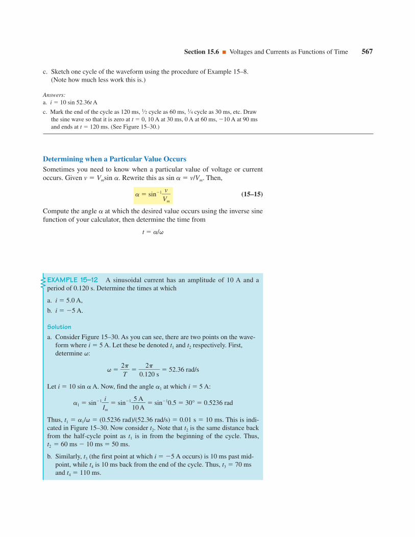
c. Sketch one cycle of the waveform using the procedure of Example 15–8.(Note how much less work this is.)
Answers:a. i 10 sin 52.36t A
c. Mark the end of the cycle as 120 ms, 1⁄2 cycle as 60 ms, 1⁄4 cycle as 30 ms, etc. Drawthe sine wave so that it is zero at t 0, 10 A at 30 ms, 0 A at 60 ms, 10 A at 90 msand ends at t 120 ms. (See Figure 15–30.)
Section 15.6 Voltages and Currents as Functions of Time 567
Determining when a Particular Value OccursSometimes you need to know when a particular value of voltage or currentoccurs. Given v Vmsin a. Rewrite this as sin a v/Vm. Then,
a sin1Vv
m
(15–15)
Compute the angle a at which the desired value occurs using the inverse sinefunction of your calculator, then determine the time from
t a/q
EXAMPLE 15–12 A sinusoidal current has an amplitude of 10 A and aperiod of 0.120 s. Determine the times at which
a. i 5.0 A,
b. i 5 A.
Solutiona. Consider Figure 15–30. As you can see, there are two points on the wave-
form where i 5 A. Let these be denoted t1 and t2 respectively. First,determine q:
q 2Tp
0.122p
0 s 52.36 rad/s
Let i 10 sin a A. Now, find the angle a1 at which i 5 A:
a1 sin1Ii
m
sin1150AA sin10.5 30° 0.5236 rad
Thus, t1 a1/q (0.5236 rad)/(52.36 rad/s) 0.01 s 10 ms. This is indi-cated in Figure 15–30. Now consider t2. Note that t2 is the same distance backfrom the half-cycle point as t1 is in from the beginning of the cycle. Thus,t2 60 ms 10 ms 50 ms.
b. Similarly, t3 (the first point at which i 5 A occurs) is 10 ms past mid-point, while t4 is 10 ms back from the end of the cycle. Thus, t3 70 msand t4 110 ms.

Voltages and Currents with Phase ShiftsIf a sine wave does not pass through zero at t 0 s as in Figure 15–30, it hasa phase shift. Waveforms may be shifted to the left or to the right (see Fig-ure 15–31). For a waveform shifted left as in (a),
v Vmsin(qt v) (15–16a)
while, for a waveform shifted right as in (b),
v Vmsin(qt v) (15–16b)
568 Chapter 15 AC Fundamentals
i (A)
10
20
6
246
4
50 70 90 110t (ms)
810
810
30
i = 5 At1
t3
t2 t4
i = 5 Ai = 5 A
i = 5 A
FIGURE 15–30
PRACTICEPROBLEMS 6
Given v 10 sin 52.36t, determine both occurrences of v 8.66 V.
Answer: 80 ms 100 ms
(a) v = Vm sin(ωt θ)
θ
ωt (rad)Vm
(b) v = Vm sin(ωt θ)
Vm
θ
ωt (rad)
FIGURE 15–31 Waveforms with phase shifts. Angle v is normally measured indegrees, yielding mixed angular units. (See note.)
EXAMPLE 15–13 Demonstrate that v 20 sin(qt 60°), where q p/6 rad/s (i.e, 30°/s), yields the shifted waveform shown in Figure 15–32.
Solution1. Since qt and 60° are both angles, (qt 60°) is also an angle. Let us define
it as x. Then v 20 sin x, which means that the shifted wave is also sinu-soidal.
2. Consider v sin(qt 60°). At t 0 s, v 20 sin(0 60°) 20 sin(60°) 17.3 V as indicated in Figure 15–32.
When applying equations 15–16(a) and (b), it is customary toexpress qt in radians and v indegrees, yielding mixed angularunits (as indicated in the follow-ing examples). Although this isacceptable when the equationsare written in symbolic form,you must convert both angles tothe same unit before you makenumerical computations.
NOTES...
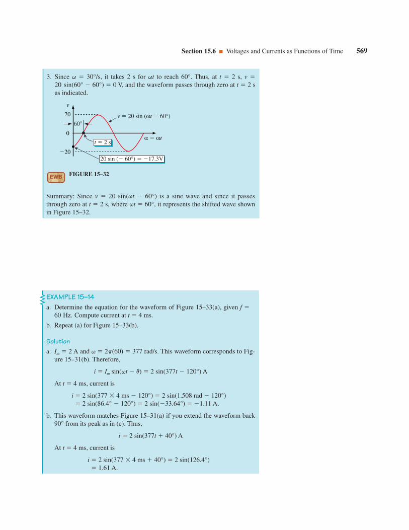
Section 15.6 Voltages and Currents as Functions of Time 569
3. Since q 30°/s, it takes 2 s for qt to reach 60°. Thus, at t 2 s, v 20 sin(60° 60°) 0 V, and the waveform passes through zero at t 2 sas indicated.
Summary: Since v 20 sin(qt 60°) is a sine wave and since it passesthrough zero at t 2 s, where qt 60°, it represents the shifted wave shownin Figure 15–32.
60°
α ωt
v 20 sin (ωt 60°)
t 2 s
20 sin ( 60°) 17.3V
v
0
20
20
EXAMPLE 15–14a. Determine the equation for the waveform of Figure 15–33(a), given f
60 Hz. Compute current at t 4 ms.
b. Repeat (a) for Figure 15–33(b).
Solutiona. Im 2 A and q 2p(60) 377 rad/s. This waveform corresponds to Fig-
ure 15–31(b). Therefore,
i Im sin(qt v) 2 sin(377t 120°) A
At t 4 ms, current is
i 2 sin(377 4 ms 120°) 2 sin(1.508 rad 120°) 2 sin(86.4° 120°) 2 sin(33.64°) 1.11 A.
b. This waveform matches Figure 15–31(a) if you extend the waveform back90° from its peak as in (c). Thus,
i 2 sin(377t 40°) A
At t 4 ms, current is
i 2 sin(377 4 ms 40°) 2 sin(126.4°) 1.61 A.
EWB FIGURE 15–32

Probably the easiest way to deal with shifted waveforms is to use pha-sors. We introduce the idea next.
15.7 Introduction to PhasorsA phasor is a rotating line whose projection on a vertical axis can be used torepresent sinusoidally varying quantities. To get at the idea, consider the redline of length Vm shown in Figure 15–34(a). (It is the phasor.) The vertical
570 Chapter 15 AC Fundamentals
(a)
i (A)
0 ωt
21
21
120°
(b)
i (A)
0 ωt
21
21
50°
(c) v = 40°
90°
50°v
FIGURE 15–33
PRACTICEPROBLEMS 7
1. Given i 2 sin(377t 60°), compute the current at t 3 ms.
2. Sketch each of the following:
a. v 10 sin(qt 20°) V. b. i 80 sin(qt 50°) A.
c. i 50 sin(qt 90°) A. d. v 5 sin(qt 180°) V.
3. Given i 2 sin(377t 60°), determine at what time i 1.8 A.
Answers:1. 1.64 A
2. a. Same as Figure 15–31(a) with Vm 10 V, v 20°.
b. Same as Figure 15–31(b) with Im 80 A, v 50°.
c. Same as Figure 15–39(b) except use Im 50 A instead of Vm.
d. A negative sine wave with magnitude of 5 V.
3. 0.193 ms
(b) Resulting sine wave(a) Phasor
Vm
2
Vm
α
α = ωtv
vAmplitude is the
same as the lengthof the phasor
α
Vm sin α
ω
Vm
FIGURE 15–34 As the phasor rotates about the origin, its vertical projection creates asine wave. (Figure 15–35 illustrates the process.)

projection of this line (indicated in dotted red) is Vm sin a. Now, assume thatthe phasor rotates at angular velocity of q rad/s in the counterclockwise direc-tion. Then, a qt, and its vertical projection is Vmsin qt. If we designatethis projection (height) as v, we get v Vmsin qt, which is the familiar sinu-soidal voltage equation.
If you plot a graph of v versus a, you get the sine wave of Figure 15–34(b). Figure 15–35 illustrates the process. It shows snapshots of the phasorand the evolving waveform at various instants of time for a phasor of magni-tude Vm 100 V rotating at q 30°/s. For example, consider t 0, 1, 2,and 3s:
1. At t 0 s, a 0, the phasor is at its 0° position, and its vertical projec-tion is v Vmsin qt 100 sin 0° 0 V. The point is at the origin.
2. At t 1 s, the phasor has rotated 30° and its vertical projection is v 100 sin 30° 50 V. This point is plotted at a 30° on the horizontalaxis.
Section 15.7 Introduction to Phasors 571
0
270 300 330 360
α (°)
0
180
210 240 270
α (°)
0 120 150 180 α (°)90
30 600 α (°)90t = 0 s
t = 1 st = 2 s
t = 3 s
100 V
100
V
ω 100 V
87 V
50 V
0 V
0 V
50 V
87 V
t = 6 s
t = 5 s
t = 4 s
100 V
ω
100
V
50 V
100 Vt = 7 s
t = 8 st = 9 s
100 V
ω
100
V
50 V
87 V
87 V
0 V
t = 10 st = 11 s
t = 12 s
ω
100 V
100
V
FIGURE 15–35 Evolution of the sinewave of Figure 15–34.
1. Although we have indicatedphasor rotation in Figure 15–35 by a series of “snapshots,”this is too cumbersome; inpractice, we show only thephasor at its t 0 s (reference)position and imply rotationrather than show it explicitly.
2. Although we are using maxi-mum values (Em and Im) here,phasors are normally drawnin terms of effective values(considered in Section 15.9).For the moment, we will con-tinue to use maximum values.We make the change in Chap-ter 16.
NOTES…
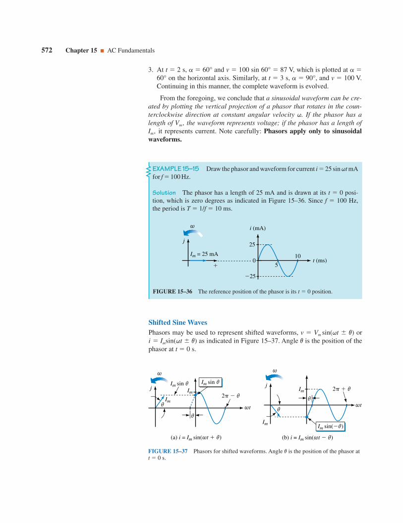
3. At t 2 s, a 60° and v 100 sin 60° 87 V, which is plotted at a 60° on the horizontal axis. Similarly, at t 3 s, a 90°, and v 100 V.Continuing in this manner, the complete waveform is evolved.
From the foregoing, we conclude that a sinusoidal waveform can be cre-ated by plotting the vertical projection of a phasor that rotates in the coun-terclockwise direction at constant angular velocity q. If the phasor has alength of Vm, the waveform represents voltage; if the phasor has a length ofIm , it represents current. Note carefully: Phasors apply only to sinusoidalwaveforms.
572 Chapter 15 AC Fundamentals
EXAMPLE 15–15 Draw the phasor and waveform for current i 25 sin qt mAfor f 100 Hz.
Solution The phasor has a length of 25 mA and is drawn at its t 0 posi-tion, which is zero degrees as indicated in Figure 15–36. Since f 100 Hz,the period is T 1/f 10 ms.
Im = 25 mA
j
ω
25
010
5
25
t (ms)
i (mA)
FIGURE 15–36 The reference position of the phasor is its t 0 position.
Im
Im
ωt
j
ω
(a) i = Im sin(ωt θ)
2 θ
θ
θ
Im sin θIm sin θIm
Im
ωt
j
ω
(b) i = Im sin(ωt θ)
2 θ
θ
θ
Im sin(θ)
FIGURE 15–37 Phasors for shifted waveforms. Angle v is the position of the phasor att 0 s.
Shifted Sine WavesPhasors may be used to represent shifted waveforms, v Vm sin(qt v) ori Imsin(qt v) as indicated in Figure 15–37. Angle v is the position of thephasor at t 0 s.

Section 15.7 Introduction to Phasors 573
EXAMPLE 15–16 Consider v 20 sin(qt 60°), where q p/6 rad/s(i.e., 30°/s). Show that the phasor of Figure 15–38(a) represents this wave-form.
Solution The phasor has length 20 V and at time t 0 is at 60° as indi-cated in (a). Now, as the phasor rotates, it generates a sinusoidal waveform,oscillating between 20 V as indicated in (b). Note that the zero crossoverpoint occurs at t 2 s, since it takes 2 seconds for the phasor to rotate from60° to 0° at 30 degrees per second. Now compare the waveform of (b) tothe waveform of Figure 15–32, Example 15–13. They are identical. Thus, thephasor of (a) represents the shifted waveform v 20 sin(qt 60°).
(a) Phasor
j
60°
ω
20 V
20 sin (60°)
ωt60°
20 V
20 V
0t = 2 s
v (V)
(b) v = 20 sin (ωt 60°), ω = 30°/s
FIGURE 15–38
EXAMPLE 15–17 With the aid of a phasor, sketch the waveform for v Vmsin(qt 90°).
Solution Place the phasor at 90° as in Figure 15–39(a). Note that the resul-tant waveform (b) is a cosine waveform, i.e., v Vmcos qt. From this, weconclude that
sin(qt 90°) cos qt
(a) Phasor at 90° position
Vm
j
ω
ωt
v
v = Vm sin (ωt 90°)
90°
(b) Waveform can also bedescribed as a cosine wave
FIGURE 15–39 Demonstrating that sin(qt 90°) cos qt.

The terms lead and lag can be understood in terms of phasors. If youobserve phasors rotating as in Figure 15–41(a), the one that you see passingfirst is leading and the other is lagging. By definition, the waveform gener-ated by the leading phasor leads the waveform generated by the laggingphasor and vice versa. In Figure 15–41, phasor Im leads phasor Vm; thus cur-rent i(t) leads voltage v(t).
Phase DifferencePhase difference refers to the angular displacement between different wave-forms of the same frequency. Consider Figure 15–40. If the angular displace-ment is 0° as in (a), the waveforms are said to be in phase; otherwise, theyare out of phase. When describing a phase difference, select one waveformas reference. Other waveforms then lead, lag, or are in phase with this refer-ence. For example, in (b), for reasons to be discussed in the next paragraph,the current waveform is said to lead the voltage waveform, while in (c) thecurrent waveform is said to lag.
574 Chapter 15 AC Fundamentals
PRACTICEPROBLEMS 8
With the aid of phasors, show that
a. sin(qt 90°) cos qt,
b. sin(qt 180°) sin qt,
v
(a) In phase
iv
i
(b) Current leads
θ
v
i
(c) Current lags
θ
FIGURE 15–40 Illustrating phase difference. In these examples, voltage is taken as ref-erence.
(a) Im leads Vm
Vm
Im
j
ω
θ
(b) Therefore, i(t) leads v(t)
Time
v(t)
i(t)
θ
FIGURE 15–41 Defining lead and lag.
If you have trouble determiningwhich waveform leads and whichlags when you are solving aproblem, make a quick sketch oftheir phasors, and the answer willbe apparent. Note also that theterms lead and lag are relative. InFigure 15–41, we said that cur-rent leads voltage; you can just ascorrectly say that voltage lagscurrent.
NOTES…

Section 15.7 Introduction to Phasors 575
EXAMPLE 15–18 Voltage and current are out of phase by 40°, and voltagelags. Using current as the reference, sketch the phasor diagram and the corre-sponding waveforms.
Solution Since current is the reference, place its phasor in the 0° positionand the voltage phasor at 40°. Figure 15–42 shows the phasors and corre-sponding waveforms.
ωt
i(t) = Im sin ωt
v(t) = Vm sin (ωt 40°)
Vm
Im
j
40°40°
Vm sin(40°)
ω
FIGURE 15–42
EXAMPLE 15–19 Given v 20 sin(qt 30°) and i 18 sin(qt 40°),draw the phasor diagram, determine phase relationships, and sketch the wave-forms.
Solution The phasors are shown in Figure 15–43(a). From these, you cansee that v leads i by 70°. The waveforms are shown in (b).
Vm = 20 V
Im = 18 A
j
(a)
30°40° 70° ωt
i = 18 sin (ωt 40°)v = 20 sin (ωt 30°)
(b)
40°
30°
70°
FIGURE 15–43
EXAMPLE 15–20 Figure 15–44 shows a pair of waveforms v1 and v2 on anoscilloscope. Each major vertical division represents 20 V and each majordivision on the horizontal (time) scale represents 20 ms. Voltage v1 leads. Pre-pare a phasor diagram using v1 as reference. Determine equations for bothvoltages.

576 Chapter 15 AC Fundamentals
30°
(a)
Generatescos (ωt 30°)
ωt60°0
cos (ωt 30°) = sin (ωt 120°)
(c)
120°
(b)
Generatessin (ωt 120°)
FIGURE 15–45 Using phasors to show that cos(qt 30°) sin(qt 120°).
Solution From the photograph, the magnitude of v1 is Vm1 3 div
20 V/div 60V. Similarly, Vm2 40V. Cycle length is T 6 20 ms 120 ms,
and the displacement between waveforms is 20 ms which is 1⁄6 of a cycle (i.e.,60°). Selecting v1 as reference and noting that v2 lags yields the phasors shownin (b). Angular frequency q 2p/T 2p/(120 106 s) 52.36 103 rad/s.Thus, v1 Vm1
sin qt 60 sin(52.36 103t) V and v2 40 sin(52.36 103t 60°) V.
Vm1 = 60 V
Vm2 = 40 V
j
60°
(b)(a)
EWB FIGURE 15–44
Sometimes voltages and currents are expressed in terms of cos qt ratherthan sin qt. As Example 15–17 shows, a cosine wave is a sine wave shiftedby 90°, or alternatively, a sine wave is a cosine wave shifted by 90°. Forsines or cosines with an angle, the following formulas apply.
cos(qt v) sin(qt v 90°) (15–17a)
sin(qt v) cos(qt v 90°) (15–17b)
To illustrate, consider cos(qt 30°). From Equation 15–17a, cos(qt 30°) sin(qt 30° 90°) sin(qt 120°). Figure 15–45 illustrates thisrelationship graphically. The red phasor in (a) generates cos qt as was shown

Section 15.7 Introduction to Phasors 577
EXAMPLE 15–21 Determine the phase angle between v 30 cos(qt 20°) and i 25 sin(qt 70°).
Solution i 25 sin(qt 70°) may be represented by a phasor at 70°, and v 30 cos(qt 20°) by a phasor at (90° 20°) 110°, Figure 15–46(a). Thus,v leads i by 40°. Waveforms are shown in (b).
Vm = 30 V Im = 25 A
70°
20° 110°
40°
(a) (b)
Phasedisplacement
70°110°
20°40°
ωt
i = 25 sin (ωt + 70°)
v = 30 cos (ωt + 20°) = 30 sin (ωt + 110°)
FIGURE 15–46
in Example 15–17. Therefore, the green phasor generates a waveform thatleads it by 30°, namely cos(qt 30°). For (b), the red phasor generates sinqt, and the green phasor generates a waveform that leads it by 120°, i.e.,sin(qt 120°). Since the green phasor is the same in both cases, you can seethat cos(qt 30°) sin(qt 120°). Note that this process is easier thantrying to remember equations 15–17(a) and (b).
Sometimes you encounter negative waveforms such as i Im sin qt.To see how to handle these, refer back to Figure 15–36, which shows thewaveform and phasor for i Im sin qt. If you multiply this waveform by 1,you get the inverted waveform Im sin qt of Figure 15–47(a) with corre-sponding phasor (b). Note that the phasor is the same as the original phasorexcept that it is rotated by 180°. This is always true—thus, if you multiply awaveform by 1, the phasor for the new waveform is 180° rotated from theoriginal phasor, regardless of the angle of the original phasor.
Im
Im
i
t
(a) i −Im sin ωt
Im
j
(b) Phasor
FIGURE 15–47 The phasor for a negative sine wave is at 180°.
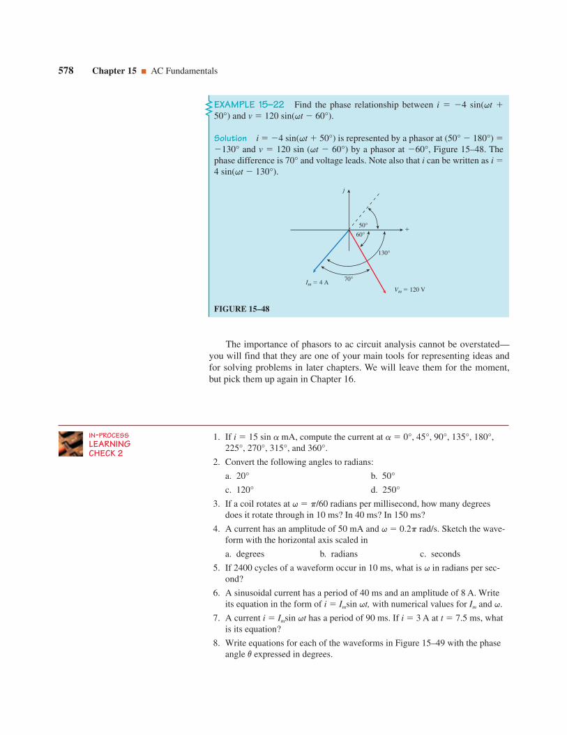
578 Chapter 15 AC Fundamentals
EXAMPLE 15–22 Find the phase relationship between i 4 sin(qt 50°) and v 120 sin(qt 60°).
Solution i 4 sin(qt 50°) is represented by a phasor at (50° 180°) 130° and v 120 sin (qt 60°) by a phasor at 60°, Figure 15–48. Thephase difference is 70° and voltage leads. Note also that i can be written as i 4 sin(qt 130°).
Im 4 AVm 120 V
j
50°60°
70°
130°
FIGURE 15–48
The importance of phasors to ac circuit analysis cannot be overstated—you will find that they are one of your main tools for representing ideas andfor solving problems in later chapters. We will leave them for the moment,but pick them up again in Chapter 16.
1. If i 15 sin a mA, compute the current at a 0°, 45°, 90°, 135°, 180°,225°, 270°, 315°, and 360°.
2. Convert the following angles to radians:
a. 20° b. 50°
c. 120° d. 250°
3. If a coil rotates at q p/60 radians per millisecond, how many degreesdoes it rotate through in 10 ms? In 40 ms? In 150 ms?
4. A current has an amplitude of 50 mA and q 0.2p rad/s. Sketch the wave-form with the horizontal axis scaled in
a. degrees b. radians c. seconds
5. If 2400 cycles of a waveform occur in 10 ms, what is q in radians per sec-ond?
6. A sinusoidal current has a period of 40 ms and an amplitude of 8 A. Writeits equation in the form of i Imsin qt, with numerical values for Im and q.
7. A current i Imsin qt has a period of 90 ms. If i 3 A at t 7.5 ms, whatis its equation?
8. Write equations for each of the waveforms in Figure 15–49 with the phaseangle v expressed in degrees.
IN-PROCESSLEARNINGCHECK 2

15.8 AC Waveforms and Average ValueWhile we can describe ac quantities in terms of frequency, period, instanta-neous value, etc., we do not yet have any way to give a meaningful value toan ac current or voltage in the same sense that we can say of a car batterythat it has a voltage of 12 volts. This is because ac quantities constantlychange and thus there is no one single numerical value that truly represents awaveform over its complete cycle. For this reason, ac quantities are generallydescribed by a group of characteristics, including instantaneous, peak, aver-age, and effective values. The first two of these we have already seen. In thissection, we look at average values; in Section 15.9, we consider effectivevalues.
Average ValuesMany quantities are measured by their average, for instance, test and exami-nation scores. To find the average of a set of marks for example, you addthem, then divide by the number of items summed. For waveforms, theprocess is conceptually the same. For example, to find the average of awaveform, you can sum the instantaneous values over a full cycle, then
Section 15.8 AC Waveforms and Average Value 579
9. Given i 10 sin qt, where f 50 Hz, find all occurrences of
a. i 8 A between t 0 and t 40 ms
b. i 5 A between t 0 and t 40 ms
10. Sketch the following waveforms with the horizontal axis scaled in degrees:
a. v1 80 sin(qt 45°) V b. v2 40 sin(qt 80°) V
c. i1 10 cos qt mA d. i2 5 cos(qt 20°) mA
11. Given q p/3 rad/s, determine when voltage first crosses through 0 for
a. v1 80 sin(qt 45°) V b. v2 40 sin(qt 80°) V
12. Consider the voltages of Question 10:
a. Sketch phasors for v1 and v2
b. What is the phase difference between v1 and v2?
c. Determine which voltage leads and which lags.
13. Repeat Question 12 for the currents of Question 10.
(Answers are at the end of the chapter.)
FIGURE 15–49
v (V)
2 µst
47 V
(c) f = 100 Hz
v (V)
40
ωt
6
(a) f = 40 Hz (b) T = 100 ms
i (A)
20
ωt
4
(d) f = 50 kHz
i (A)
i = Im sin (ωt 30°)
ωt
125 A

divide by the number of points used. The trouble with this approach is thatwaveforms do not consist of discrete values.
Average in Terms of the Area Under a CurveAn approach more suitable for use with waveforms is to find the area underthe curve, then divide by the baseline of the curve. To get at the idea, we canuse an analogy. Consider again the technique of computing the average for aset of numbers. Assume that you earn marks of 80, 60, 60, 95, and 75 on agroup of tests. Your average mark is therefore
average (80 60 60 95 75)/5 74
An alternate way to view these marks is graphically as in Figure 15–50.The area under this curve can be computed as
area (80 1) (60 2) (95 1) (75 1)
Now divide this by the length of the base, namely 5. Thus,
74
which is exactly the answer obtained above. That is,
average ar
leeang
utnhdoefr
bcausreve
(15–18)
This result is true in general. Thus, to find the average value of a waveform,divide the area under the waveform by the length of its base. Areas above theaxis are counted as positive, while areas below the axis are counted as nega-tive. This approach is valid regardless of waveshape.
Average values are also called dc values, because dc meters indicateaverage values rather than instantaneous values. Thus, if you measure a non-dc quantity with a dc meter, the meter will read the average of the waveform,i.e., the value calculated according to Equation 15–18.
(80 1) (60 2) (95 1) (75 1)
5
580 Chapter 15 AC FundamentalsG
rade
s
1
20
0
6040
2 4 5
10080
3
Base = 5
9575
606080 Test
Marks
FIGURE 15–50 Determining aver-age by area.
EXAMPLE 15–23a. Compute the average for the current waveform of Figure 15–51.
b. If the negative portion of Figure 15–51 is 3 A instead of 1.5 A, what isthe average?
c. If the current is measured by a dc ammeter, what will the ammeter indi-cate?
FIGURE 15–51
i (A)
1 20
1
2
1
t (ms)
2
5 6
1 cycle
873 4

Section 15.8 AC Waveforms and Average Value 581
Solutiona. The waveform repeats itself after 7 ms. Thus, T 7 ms and the average is
Iavg 6
76
0 A
b. Iavg 6
7A
0.857 A
c. A dc ammeter measuring (a) will indicate zero, while for (b) it will indi-cate 0.857 A.
(2 A 3 ms) (3 A 4 ms)
7 ms
(2 A 3 ms) (1.5 A 4 ms)
7 ms
EXAMPLE 15–24 Compute the average value for the waveforms of Fig-ures 15–52(a) and (c). Sketch the averages for each.
v (V)
1 2
100
3020
3 4 7 8t (s)
5 61 cycle
(a)
Vavg = 16.7 V
100
20
(b)
i (mA)
1 20
40
20
9t (s)
40
203 4 7 85 6
(c)
Iavg = 7.5 mA10
0
(d)
FIGURE 15–52
Solution For the waveform of (a), T 6 s. Thus,
Vavg 100
6Vs
-s 16.7V
The average is shown as (b). A dc voltmeter would indicate 16.7 V. For thewaveform of (c), T 8 s and
Iavg
860mA7.5mA
In this case, a dc ammeter would indicate 7.5 mA.
12
(40mA3s)(20mA2s)(40mA2s)
8s
(10V2s)(20V1s)(30V2s)(0V1s)
6s

582 Chapter 15 AC Fundamentals
PRACTICEPROBLEMS 9
Determine the averages for Figures 15–53(a) and (b).
(a)
i (A)
1 20
20
8t (s)
−204 75 63
(b)
v (V)
1 2
100
20
7 8 9t (s)
3 4 5 6
Half circles
FIGURE 15–53
Answers: a. 1.43 A b. 6.67 V
0
i
Im
Area = 2Im
FIGURE 15–54 Area under a half-cycle.
0 2
i
Im
Base
Iavg = 0.637Im
FIGURE 15–55 Full-wave average.
0 2
i
Im
Base
Iavg = 0.318Im
FIGURE 15–56 Half-wave average.
Sine Wave AveragesBecause a sine wave is symmetrical, its area below the horizontal axis isthe same as its area above the axis; thus, over a full cycle its net area iszero, independent of frequency and phase angle. Thus, the average of sinqt, sin(qt v), sin 2qt, cos qt, cos(qt v), cos 2qt, and so on are eachzero. The average of half a sine wave, however, is not zero. Consider Fig-ure 15–54. The area under the half-cycle may be found using calculus as
area p
0Imsina da Imcos a
p
0 2Im (15–19)
Similarly, the area under a half-cycle of voltage is 2Vm. (If you haven’t stud-ied calculus, you can approximate this area using numerical methods asdescribed later in this section.)
Two cases are important; full-wave average and half-wave average. Thefull-wave case is illustrated in Figure 15–55. The area from 0 to 2p is 2(2Im)and the base is 2p. Thus, the average is
Iavg 2(
2
2
p
Im)
2
p
Im 0.637Im
For the half-wave case (Figure 15–56),
Iavg 2
2I
p
m
I
p
m 0.318Im
The corresponding expressions for voltage are
Vavg 0.637Vm (full-wave)
Vavg 0.318Vm (half-wave)
Numerical MethodsIf the area under a curve cannot be computed exactly, it can be approxi-mated. One method is to approximate the curve by straight line segments asin Figure 15–57. (If the straight lines closely fit the curve, the accuracy isvery good.) Each element of area is a trapezoid (b) whose area is its average
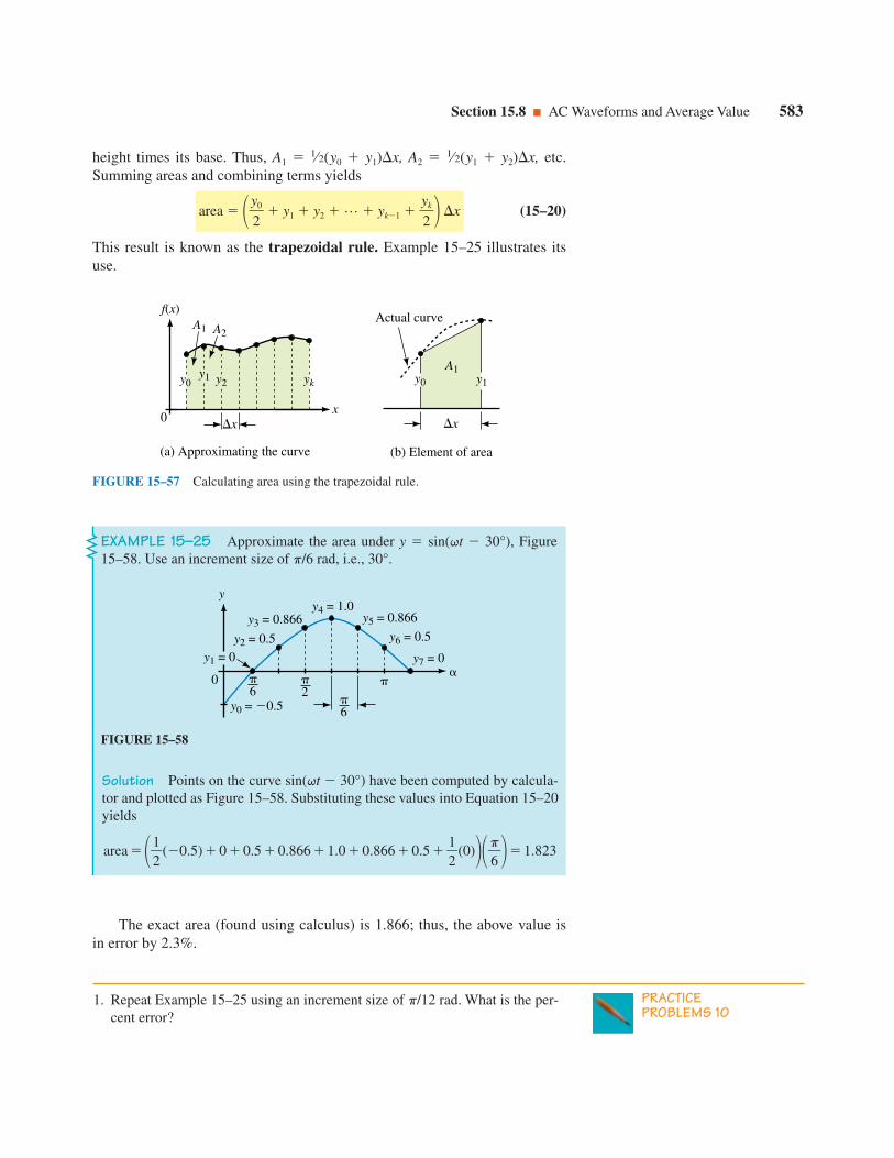
height times its base. Thus, A1 1⁄2(y0 y1)x, A2 1⁄2(y1 y2)x, etc.Summing areas and combining terms yields
area y
20 y1 y2 … yk1
y
2k x (15–20)
This result is known as the trapezoidal rule. Example 15–25 illustrates itsuse.
Section 15.8 AC Waveforms and Average Value 583
0
f(x)
y0y1 y2 yk
xx
A1 A2
(a) Approximating the curve
y0 y1
x
A1
Actual curve
(b) Element of area
FIGURE 15–57 Calculating area using the trapezoidal rule.
EXAMPLE 15–25 Approximate the area under y sin(qt 30°), Figure15–58. Use an increment size of p/6 rad, i.e., 30°.
0
y5 = 0.866y3 = 0.866
y2 = 0.5
y4 = 1.0
y6 = 0.5
y0 = 0.5
y7 = 0y1 = 0
y
6
6
2
FIGURE 15–58
Solution Points on the curve sin(qt 30°) have been computed by calcula-tor and plotted as Figure 15–58. Substituting these values into Equation 15–20yields
area 12
(0.5) 0 0.5 0.866 1.0 0.866 0.5 12
(0)p
6 1.823
The exact area (found using calculus) is 1.866; thus, the above value isin error by 2.3%.
PRACTICEPROBLEMS 10
1. Repeat Example 15–25 using an increment size of p/12 rad. What is the per-cent error?

584 Chapter 15 AC Fundamentals
2. Approximate the area under v 50 sin(qt 30°) from qt 0° to qt 210°.Use an increment size of p/12 rad.
Answers:1. 1.855; 0.59%
2. 67.9 (exact 68.3; error 0.6%)
Superimposed AC and DCSometimes ac and dc are used in the same circuit. For example, amplifiersare powered by dc but the signals they amplify are ac. Figure 15–59 shows asimple circuit with combined ac and dc.
Figure 15–60(c) shows superimposed ac and dc. Since we know that theaverage of a sine wave is zero, the average value of the combined waveformwill be its dc component, E. However, peak voltages depend on both compo-nents as illustrated in (c). Note for the case illustrated that although thewaveform varies sinusoidally, it does not alternate in polarity since it neverchanges polarity to become negative.
e
E v = E + e
FIGURE 15–59
(a) AC alone. E = 0 V.Vavg = 0 V
T0
v
Em
Time
2T
v = e
Em
(b) DC alone. e = 0 V.Vavg = E
Time0
v
Ev = E
(c) Superimposed ac and dc.Vavg = E
Time0
v
EE Em
v = E e
E Em
FIGURE 15–60 Superimposed dc and ac.
EXAMPLE 15–26 Draw the voltage waveform for the circuit of Figure15–61(a). Determine average, peak, and minimum voltages.
e = 15 sin ωt
E 10 V v = E + e
(a) (b)
5 V
Vavg = 10 V25 V
v (V)
100
30
10
20
ωt
15 V
15 V
FIGURE 15–61 v 10 15 sin qt.
Solution The waveform consists of a 10-V dc value with 15 V ac riding ontop of it. The average is the dc value, Vavg 10 V. The peak voltage is 10 15 25 V, while the minimum voltage is 10 15 5 V. This waveformalternates in polarity, although not symmetrically (as is the case when there isno dc component).

15.9 Effective ValuesWhile instantaneous, peak, and average values provide useful informationabout a waveform, none of them truly represents the ability of the waveformto do useful work. In this section, we look at a representation that does. It iscalled the waveform’s effective value. The concept of effective value is animportant one; in practice, most ac voltages and currents are expressed aseffective values. Effective values are also called rms values for reasons dis-cussed shortly.
What Is an Effective Value?An effective value is an equivalent dc value: it tells you how many volts oramps of dc that a time-varying waveform is equal to in terms of its ability toproduce average power. Effective values depend on the waveform. A famil-iar example of such a value is the value of the voltage at the wall outlet inyour home. In North America its value is 120 Vac. This means that the sinu-soidal voltage at the wall outlets of your home is capable of producing thesame average power as 120 volts of steady dc.
Effective Values for Sine WavesThe effective value of a waveform can be determined using the circuits ofFigure 15–62. Consider a sinusoidally varying current, i(t). By definition, theeffective value of i is that value of dc current that produces the same averagepower. Consider (b). Let the dc source be adjusted until its average power isthe same as the average power in (a). The resulting dc current is then theeffective value of the current of (a). To determine this value, determine theaverage power for both cases, then equate them.
Section 15.9 Effective Values 585
PRACTICEPROBLEMS 11
Repeat Example 15–26 if the dc source of Figure 15–61 is E 5 V.
Answers: Vavg 5 V; positive peak 10 V; negative peak 20 V
R
(a) AC circuit
e
i
t
p(t)
p(t)
i(t)
Im2R
Pavg =Im
2R2
p(t) = i2R. Therefore, p(t) varies cyclically.
R
(b) DC circuit
EI
t
P
P
P = I2R. Therefore, P is constant.
FIGURE 15–62 Determining the effective value of sinusoidal ac.
First, consider the dc case. Since current is constant, power is constant,and average power is
Pavg P I2R (15–21)

586 Chapter 15 AC Fundamentals
Because ac currents alternate indirection, you might expect aver-age power to be zero, with powerduring the negative half-cyclebeing equal and opposite topower during the positive half-cycle and hence cancelling. How-ever, as Equation 15–22 shows,current is squared, and hencepower is never negative. This isconsistent with the idea that inso-far as power dissipation is con-cerned, the direction of currentthrough a resistor does not matter(Figure 15–63).
FIGURE 15–63 Since powerdepends only on current magnitude,it is the same for both directions.
NOTES...
80 I = 4 A
80 I = 4 A
(b) P = (4)2(80) = 1280 W
(a) P = (4)2(80) = 1280 W
EXAMPLE 15–27 Determine the effective values of
a. i 10 sin qt A, b. i 50 sin(qt 20°) mA,
c. v 100 cos 2qt V
Now consider the ac case. Power to the resistor at any value of time is p(t) i2R, where i is the instantaneous value of current. A sketch of p(t) is shownin Figure 15–62(a), obtained by squaring values of current at various pointsalong the axis, then multiplying by R. Average power is the average of p(t).Since i Im sin qt,
p(t) i2R
(Im sin qt)2R Im2R sin2qt (15–22)
Im2R
12
(1 cos 2qt)where we have used the trigonometric identity sin2qt 1⁄2(1 cos 2qt),from the mathematics tables inside the front cover to expand sin2qt. Thus,
p(t) Im
2
2R
Im
2
2R cos 2qt (15–23)
To get the average of p(t), note that the average of cos 2qt is zero and thusthe last term of Equation 15–23 drops off leaving
Pavg average of p(t) Im
2
2R (15–24)
Now equate Equations 15–21 and 15–24, then cancel R.
I2 I
2m
2
Now take the square root of both sides. Thus,
I I
2m
2
Im
2 0.707Im
Current I is the value that we are looking for; it is the effective value ofcurrent i. To emphasize that it is an effective value, we will initially use sub-scripted notation Ieff. Thus,
Ieff Im
2 0.707Im (15–25)
Effective values for voltage are found in the same way:
Eeff Em
2 0.707Em (15–26a)
Veff Vm
2 0.707Vm (15–26b)
As you can see, effective values for sinusoidal waveforms depend only onmagnitude.

Section 15.9 Effective Values 587
e (V)
0 Time
170
170
(a) (b)
Time
120 V
FIGURE 15–64 120 V of steady dcis capable of producing the same aver-age power as sinusoidal ac with Em 170 V.
Solution Since effective values depend only on magnitude,
a. Ieff (0.707)(10 A) 7.07 A,
b. Ieff (0.707)(50 mA) 35.35 mA,
c. Veff (0.707)(100 V) 70.7 V.
To obtain peak values from effective values, rewrite Equations 15–25and 15–26. Thus,
Im 2Ieff 1.414Ieff (15–27)
Em 2Eeff 1.414Veff (15–28a)
Vm 2Veff 1.414Veff (15–28b)
It is important to note that these relationships hold only for sinusoidal wave-forms. However, the concept of effective value applies to all waveforms, aswe soon see.
Consider again the ac voltage at the wall outlet in your home. Since Eeff 120 V, Em (2)(120 V) 170 V. This means that a sinusoidal voltagealternating between 170 V produces the same average power as 120 V ofsteady dc (Figure 15–64).
General Equation for Effective ValuesThe 2 relationship holds only for sinusoidal waveforms. For other wave-forms, you need a more general formula. Using calculus, it can be shownthat for any waveform
Ieff T1
T
0i2dt (15–29)
with a similar equation for voltage. This equation can be used to computeeffective values for any waveform, including sinusoidal. In addition, it leadsto a graphic approach to finding effective values. In Equation 15–29, theintegral of i2 represents the area under the i2 waveform. Thus,
Ieff (15–30)
To compute effective values using this equation, do the following:
Step 1: Square the current (or voltage) curve.
Step 2: Find the area under the squared curve.
area under the i2 curve
base

Step 3: Divide the area by the length of the curve.
Step 4: Find the square root of the value from Step 3.
This process is easily carried out for rectangular-shaped waveforms since thearea under their squared curves is easy to compute. For other waveforms,you have to use calculus or approximate the area using numerical methods.For the special case of superimposed ac and dc (Figure 15–60), Equation15–29 leads to the following formula:
Ieff Idc2 Iac2 (15–31)
where Idc is the dc current value, Iac is the effective value of the ac compo-nent, and Ieff is the effective value of the combined ac and dc currents. Equa-tions 15–30 and 15–31 also hold for voltage when V is substituted for I.
RMS ValuesConsider again Equation 15–30. To use this equation, we compute the rootof the mean square to obtain the effective value. For this reason, effectivevalues are called root mean square or rms values and the terms effectiveand rms are synonymous. Since, in practice, ac quantities are almostalways expressed as rms values, we shall assume from here on that, unlessotherwise noted, all ac voltages and currents are rms values.
EXAMPLE 15–28 One cycle of a voltage waveform is shown in Figure15–65(a). Determine its effective value.
588 Chapter 15 AC Fundamentals
Solution Square the voltage waveform and plot it as in (b). Apply Equa-tion 15–30:
Veff
361000 19.0 V
The waveform of Figure 15–65(a) has the same effective value as 19.0 Vof steady dc.
(400 4) (900 2) (100 2) (0 2)
10
v (V)
1 2
10
0
30
20
3 4 109t
105
T
(a) Voltage waveform
7 86
v2 (V)
20
900
400
4 10t
(b) Squared waveform
86
1000
T = 10
FIGURE 15–65

Section 15.9 Effective Values 589
EXAMPLE 15–29 Determine the effective value of the waveform of Figure15–66(a).
Solution Square the curve, then apply Equation 15–30. Thus,
Ieff
481 2.26 A
(9 3) (1 2) (4 3)
8
(a)
i (A)
1 2
10
3
12
2
3 4t (s)
5 6
1 cycle
87
(b)
i2
1
1 2 3 4 5 6 7 80 t (s)
4
9
FIGURE 15–66
EXAMPLE 15–30 Compute the effective value of the waveform of Figure15–61(b).
Solution Use Equation 15–31 (with I replaced by V). First, compute therms value of the ac component. Vac 0.707 15 10.61 V. Now substitutethis into Equation 15–31. Thus,
Vrms V2dc V2
ac (10)2 (10.61)2 14.6 V
PRACTICEPROBLEMS 12
1. Determine the effective value of the current of Figure 15–51.
2. Repeat for the voltage graphed in Figure 15–52(a).
Answers:1. 1.73 A
2. 20 V
One Final NoteThe subscripts eff and rms are not used in practice. Once the concept isfamiliar, we drop them.

15.10 Rate of Change of a Sine Wave (Derivative)Several important circuit effects depend on the rate of change of sinusoidalquantities. The rate of change of a quantity is the slope (i.e., derivative) ofits waveform versus time. Consider the waveform of Figure 15–67. As indi-cated, the slope is maximum positive at the beginning of the cycle, zero atboth its peaks, maximum negative at the half-cycle crossover point, andmaximum positive at the end of the cycle. This slope is plotted in Figure15–68. Note that the original waveform and its slope are 90° out of phase.Thus, if sinusoidal waveform A is taken as reference, its slope B leads it by90°, whereas, if the slope B is taken as reference, A lags it by 90°. Thus, ifA is a sine wave, B is a cosine wave, and so on. (This result is important tous in Chapter 16.)
590 Chapter 15 AC Fundamentals
Zero slope
Zeroslope
Maximumpositive slope
Maximumpositive
slope
Maximumnegative
slope
t
Waveform A
Slope(Waveform B)
FIGURE 15–67 Slope at variousplaces for a sine wave.
FIGURE 15–68 Showing the 90°phase shift.
The Derivative of a Sine WaveThe result developed intuitivelyhere can be proven easily usingcalculus. To illustrate, considerthe waveform sin qt shown inFigure 15–67. The slope of thisfunction is its derivative. Thus,
Slope ddt sin qt qcos qt
Therefore, the slope of a sinewave is a cosine wave as depictedin Figure 15–68.
∫
NOTES...
15.11 AC Voltage and Current MeasurementTwo of the most important instruments for measuring ac quantities are themultimeter and the oscilloscope. Multimeters read voltage, current, andsometimes frequency. Oscilloscopes show waveshape and period and permitdetermination of frequency, phase difference, and so on.
Meters for Voltage and Current MeasurementThere are two basic classes of ac meters: one measures rms correctly forsinusoidal waveforms only (called “average responding” instruments); theother measures rms correctly regardless of waveform (called “true rms”meters). Most common meters are average responding meters.
Average Responding Meters
Average responding meters use a rectifier circuit to convert incoming ac todc. They then respond to the average value of the rectified input, which, asshown in Figure 15–55, is 0.637Vm for a “full-wave” rectified sine wave.However, the rms value of a sine wave is 0.707Vm. Thus, the scale of such ameter is modified by the factor 0.707Vm/0.637Vm 1.11 so that it indicatesrms values directly. Other meters use a “half-wave” circuit, which yields thewaveform of Figure 15–56 for a sine wave input. In this case, its average is0.318Vm, yielding a scale factor of 0.707Vm/0.318Vm 2.22. Figure 15–69shows a typical average responding DMM.

Section 15.11 AC Voltage and Current Measurement 591
FIGURE 15–69 A DMM. While all DMMs measure voltage, current, and resistance,this one also measures frequency.
True RMS Measurement
To measure the rms value of a nonsinusoidal waveform, you need a true rmsmeter. A true rms meter indicates true rms voltages and currents regardlessof waveform. For example, for the waveform of Figure 15–64(a), any acmeter will correctly read 120 V (since it is a sine wave). For the waveform of15–61(b), a true rms meter will correctly read 14.6 V (the rms value that wecalculated earlier, in Example 15–30) but an average responding meter willyield only a meaningless value. True rms instruments are more expensivethan standard meters.
OscilloscopesOscilloscopes (frequently referred to as scopes, Figure 15–70) are used fortime domain measurement, i.e., waveshape, frequency, period, phase differ-ence, and so on. Usually, you scale values from the screen, although somehigher-priced models can compute and display them for you on a digitalreadout.
Oscilloscopes measure voltage. To measure current, you need a current-to-voltage converter. One type of converter is a clip-on device, known as acurrent gun that clamps over the current-carrying conductor and monitorsits magnetic field. (It works only with ac.) The varying magnetic fieldinduces a voltage which is then displayed on the screen. With such a device,you can monitor current waveshapes and make current-related measure-ments. Alternately, you can place a small resistor in the current path, mea-

592 Chapter 15 AC Fundamentals
FIGURE 15–70 An oscilloscope may be used for waveform analysis.
sure voltage across it with the oscilloscope, then use Ohm’s law to determinethe current.
A Final NoteAC meters measure voltage and current only over a limited frequency range,typically from 50 Hz to a few kHz, although others are available that workup to the 100-kHz range. Note, however, that accuracy may be affected byfrequency. (Check the manual.) Oscilloscopes, on the other hand, can mea-sure very high frequencies; even moderately priced oscilloscopes work atfrequencies up to hundreds of MHz.
15.12 Circuit Analysis Using ComputersElectronics Workbench and PSpice both provide a convenient way to studythe phase relationships of this chapter, as they both incorporate easy-to-usegraphing facilities. You simply set up sources with the desired magnitudeand phase values and instruct the software to compute and plot the results.To illustrate, let us graph e1 100 sin qt V and e2 80 sin(qt 60°) V.Use a frequency of 500 Hz.
Electronics WorkbenchFor Electronics Workbench, you must specify rms rather than peak values.Thus, to plot e1 100 sin qt V, key in 70.71 V and 0 degrees. Similarly,for e2, use 56.57 V and 60°. Here are the steps: Create the circuit of Figure15–71 on the screen; Double click Source 1 and enter 70.71 V, 0 deg, and500 Hz in the dialog box; Similarly, set Source 2 to 56.57 V, 60 deg, and
PSpiceELECTRONICSWORKBENCH
500 Hz; Click Analysis, Transient, set TSTOP to 0.002 (to run the solu-tion out to 2 ms so that you display a full cycle) and TMAX to 2e-06 (toavoid getting a choppy waveform); Highlight Node 1 (to display e1) andclick Add; Repeat for Node 2 (to display e2); Click the Simulate icon; Fol-lowing simulation, graphs e1 and e2 (Figure 15–72) appear.
Section 15.12 Circuit Analysis Using Computers 593
FIGURE 15–71 Studying phase relationships using Electronics Workbench.
FIGURE 15–72
v
t
FIGURE 15–73
You can verify the angle between the waveforms using cursors. First,note that the period T 2 ms 2000 ms. (This corresponds to 360°.)Expand the graph to full screen, click the Grid icon, then the Cursorsicon. Using the cursors, measure the time between crossover points, asindicated in Figure 15–73. You should get 333 ms. This yields an angulardisplacement of
v 2
3
0
3
0
3
0
m
m
s
s 360° 60°
OrCAD PSpiceFor this problem, you need a sinusoidal time-varying ac voltage source. UseVSIN (it is found in the SOURCE library.) For VSIN, you must specify themagnitude, phase, and frequency of the source, as well as its offset (since wedo not want an offset in this problem, we will set it to zero.) Proceed as fol-lows. Build the circuit of Figure 15–74 on the screen. Double click source 1and in the Properties editor, select the Parts tab. Scroll right until you find alist of source properties: then in cell VAMPL, enter 100V; in cell PHASE,enter 0deg; in cell FREQ, enter 500Hz; and in cell VOFF, enter 0V (thissets source ei 100 sin qt V with q 2p(500 Hz)). Click Apply, then closethe Properties editor window. Similarly, set up source 2 (making sure youuse a phase angle of 60°). Click the New Simulation icon and enter a name(e.g., fig15-74). In the Simulation Settings box, select Time Domain andGeneral Settings. Set TSTOP to 2ms (to display a full cycle). Select volt-age markers from the toolbar and place as shown. (This causes PSpice toautomatically create the photos.) Run the simulation. When the simulation iscomplete, the waveforms of Figure 15–75 should appear.
594 Chapter 15 AC Fundamentals
FIGURE 15–74 Studying phase relationships using OrCAD PSpice.
FIGURE 15–75

You can verify the angle between the waveforms using cursors. First,note that the period T 2 ms 2000 ms. (This corresponds to 360°.)Now using the cursors (see Appendix A if you need help), measure thetime between crossover points as indicated in Figure 15–73. You shouldget 333 ms. This yields an angular displacement of
v 2303030m
m
ss
360° 60°
which agrees with the given sources.
Problems 595
PROBLEMS15.1 Introduction
1. What do we mean by “ac voltage”? By “ac current”?
15.2 Generating AC Voltages
2. The waveform of Figure 15–8 is created by a 600-rpm generator. If thespeed of the generator changes so that its cycle time is 50 ms, what is itsnew speed?
3. a. What do we mean by instantaneous value?
b. For Figure 15–76, determine instantaneous voltages at t 0, 1, 2, 3, 4, 5,6, 7, and 8 ms.
15.3 Voltage and Current Conventions for ac
4. For Figure 15–77, what is I when the switch is in position 1? When in posi-tion 2? Include sign.
e (V)
1 2
100
1020
20
3 4 7 8t (ms)
5 6
FIGURE 15–76
25 I40 V70 V
1
2
FIGURE 15–77
i(t)
e(t) R 4 k
FIGURE 15–78
5. The source of Figure 15–78 has the waveform of Figure 15–76. Determinethe current at t 0, 1, 2, 3, 4, 5, 6, 7, and 8 ms. Include sign.
15.4 Frequency, Period, Amplitude, and Peak Value
6. For each of the following, determine the period:
a. f 100 Hz b. f 40 kHz c. f 200 MHz
7. For each of the following, determine the frequency:
a. T 0.5 s b. T 100 ms c. 5T 80 ms
8. For a triangular wave, f 1.25 MHz. What is its period? How long does ittake to go through 8 107 cycles?
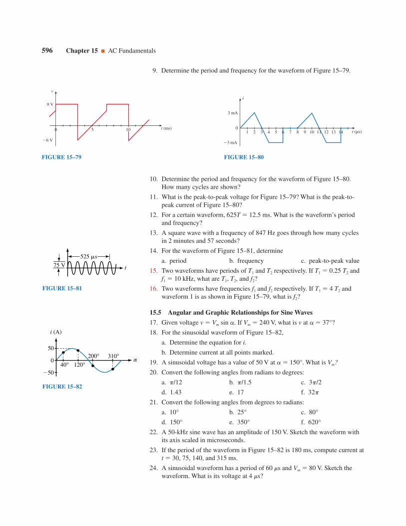
596 Chapter 15 AC Fundamentals
9. Determine the period and frequency for the waveform of Figure 15–79.
9 V
6 V
50
v
t (ms)10
FIGURE 15–79
3 mA
01 2 3 4 5 6 7 8 9 10 11 12 13 14
3 mA
i
t (µs)
FIGURE 15–80
t75 V
525 s
FIGURE 15–81
α040°
50
50120°
200° 310°
i (A)
FIGURE 15–82
10. Determine the period and frequency for the waveform of Figure 15–80.How many cycles are shown?
11. What is the peak-to-peak voltage for Figure 15–79? What is the peak-to-peak current of Figure 15–80?
12. For a certain waveform, 625T 12.5 ms. What is the waveform’s periodand frequency?
13. A square wave with a frequency of 847 Hz goes through how many cyclesin 2 minutes and 57 seconds?
14. For the waveform of Figure 15–81, determine
a. period b. frequency c. peak-to-peak value
15. Two waveforms have periods of T1 and T2 respectively. If T1 0.25 T2 andf1 10 kHz, what are T1, T2, and f2?
16. Two waveforms have frequencies f1 and f2 respectively. If T1 4 T2 andwaveform 1 is as shown in Figure 15–79, what is f2?
15.5 Angular and Graphic Relationships for Sine Waves
17. Given voltage v Vm sin a. If Vm 240 V, what is v at a 37°?
18. For the sinusoidal waveform of Figure 15–82,
a. Determine the equation for i.
b. Determine current at all points marked.
19. A sinusoidal voltage has a value of 50 V at a 150°. What is Vm?
20. Convert the following angles from radians to degrees:
a. p/12 b. p/1.5 c. 3p/2
d. 1.43 e. 17 f. 32p
21. Convert the following angles from degrees to radians:
a. 10° b. 25° c. 80°
d. 150° e. 350° f. 620°
22. A 50-kHz sine wave has an amplitude of 150 V. Sketch the waveform withits axis scaled in microseconds.
23. If the period of the waveform in Figure 15–82 is 180 ms, compute current att 30, 75, 140, and 315 ms.
24. A sinusoidal waveform has a period of 60 ms and Vm 80 V. Sketch thewaveform. What is its voltage at 4 ms?

Problems 597
25. A 20-kHz sine wave has a value of 50 volts at t 5 ms. Determine Vm andsketch the waveform.
26. For the waveform of Figure 15–83, determine v2.
15.6 Voltages and Currents as Functions of Time
27. Calculate q in radians per second for each of the following:
a. T 100 ns b. f 30 Hz c. 100 cycles in 4 s
d. period 20 ms e. 5 periods in 20 ms
28. For each of the following values of q, compute f and T:
a. 100 rad/s b. 40 rad in 20 ms c. 34 103 rad/s
29. Determine equations for sine waves with the following:
a. Vm 170 V, f 60 Hz b. Im 40 mA, T 10 ms
c. T 120 ms, v 10 V at t 12 ms
30. Determine f, T, and amplitude for each of the following:
a. v 75 sin 200pt b. i 8 sin 300t
31. A sine wave has a peak-to-peak voltage of 40 V and T 50 ms. Determineits equation.
32. Sketch the following waveforms with the horizontal axis scaled in degrees,radians, and seconds:
a. v 100 sin 200pt V
b. i 90 sin qt mA, T 80 ms
33. Given i 47 sin 8260t mA, determine current at t 0 s, 80 ms, 410 ms, and1200 ms.
34. Given v 100 sin a. Sketch one cycle.
a. Determine at which two angles v 86.6 V.
b. If q 100p/60 rad/s, at which times do these occur?
35. Write equations for the waveforms of Figure 15–84. Express the phaseangle in degrees.
α0 60°
57330°
v (V)
v2
FIGURE 15–83
FIGURE 15–84
ωt
i
5 (mA)
(a) ω 1000 rad/s
π rad5
ωt
i
10 A
(b) t 50 ms
60°ωt
v
40 V
(c) f 900 Hz
π rad4
36. Sketch the following waveforms with the horizontal axis scaled in degreesand seconds:
a. v 100 sin(232.7t 40°) V
b. i 20 sin(qt 60°) mA, f 200 Hz
37. Given v 5 sin(qt 45°). If q 20p rad/s, what is v at t 20, 75, and90 ms?

38. Repeat Problem 35 for the waveforms of Figure 15–85.
598 Chapter 15 AC Fundamentals
ωt
v
80 V
(a) Period 10 µs
320°
ωt
v
100 V
160µs
(b) f 833.3 Hz
FIGURE 15–85
ωt
v100 V
54°
1620 µs
FIGURE 15–86
i1 = 15.6 A
Im sin (60°)
i
0 ωt
Im
i2
180°350°
FIGURE 15–87
39. Determine the equation for the waveform shown in Figure 15–86.
40. For the waveform of Figure 15–87, determine i2.
41. Given v 30 sin(qt 45°) where q 40p rad/s. Sketch the waveform. Atwhat time does v reach 0 V? At what time does it reach 23 V and 23 V?
15.7 Introduction to Phasors
42. For each of the phasors of Figure 15–88, determine the equation for v(t) ori(t) as applicable, and sketch the waveform.
Vm = 100 V
j
70°
(a)
Im = 20 A
j
40°
(b)
Im = 10 mA
j
35°
(c)
FIGURE 15–88
43. With the aid of phasors, sketch the waveforms for each of the followingpairs and determine the phase difference and which waveform leads:
a. v 100 sin qt b. v1 200 sin(qt 30°)i 80 sin(qt 20°) v2 150 sin(qt 30°)
c. i1 40 sin(qt 30°) d. v 100 sin(qt 140°)i2 50 sin(qt 20°) i 80 sin(qt 160°)

Problems 599
44. Repeat Problem 43 for the following.
a. i 40 sin(qt 80°) b. v 20 cos(qt 10°)v 30 sin(qt 70°) i 15 sin(qt 10°)
c. v 20 cos(qt 10°) d. v 80 cos(qt 30°)i 15 sin(qt 120°) i 10 cos(qt 15°)
45. For the waveforms in Figure 15–89, determine the phase differences. Whichwaveform leads?
46. Draw phasors for the waveforms of Figure 15–89.
15.8 AC Waveforms and Average Value
47. What is the average value of each of the following over an integral numberof cycles?
a. i 5 sin qt b. i 40 cos qt
c. v 400 sin(qt 30°) d. v 20 cos 2qt
48. Using Equation 15–20, compute the area under the half-cycle of Figure 15–54 using increments of p/12 rad.
49. Compute Iavg for the waveforms of Figure 15–90.
(a)
ωt30°
300°B
A
(b)
ωt
BA
60° 180°
FIGURE 15–89
i (A)
1 2
10
3
123
2
3 4 7 8 9 10t (s)
5 6
(a)
v (V)
0
20
20
t (ms)100 200
(b)
i (A)
0
2
1
ωt
2
23 2
Sinewave
1 cycle
(c)
FIGURE 15–90
50. For the waveform of Figure 15–91, compute Im.
51. For the circuit of Figure 15–92, e 25 sin qt V and period T 120 ms.
a. Sketch voltage v(t) with the axis scaled in milliseconds.
b. Determine the peak and minimum voltages.
c. Compute v at t 10, 20, 70, and 100 ms.
d. Determine Vavg.
i (A)
Im
Iavg = 10 A
Im
0 t (s)5 6
1 cycle
41 2 3
FIGURE 15–91
e
e = 25 sin t
15 V v(t)
FIGURE 15–92

600 Chapter 15 AC Fundamentals
52. Using numerical methods for the curved part of the waveform (with incre-ment size t 0.25 s), determine the area and the average value for thewaveform of Figure 15–93.
53. Using calculus, find the average value for Figure 15–93.∫
15.9 Effective Values
54. Determine the effective values of each of the following:
a. v 100 sin qt V b. i 8 sin 377t A
c. v 40 sin(qt 40°) V d. i 120 cos qt mA
55. Determine the rms values of each for the following.
a. A 12 V battery b. 24 sin(qt 73°) mA
c. 10 24 sin qt V d. 45 27 cos 2 qt V
56. For a sine wave, Veff 9 V. What is its amplitude?
6 V
12 V
01 2 5
6 V
3 t2
v
t (s)3 4
FIGURE 15–93
−12 A
(a)
4 A
0
i
t (µs)2 64
(b)
0
5 V
30 V
10 V
1 cycle
v
t (ms)1 32 4
FIGURE 15–94
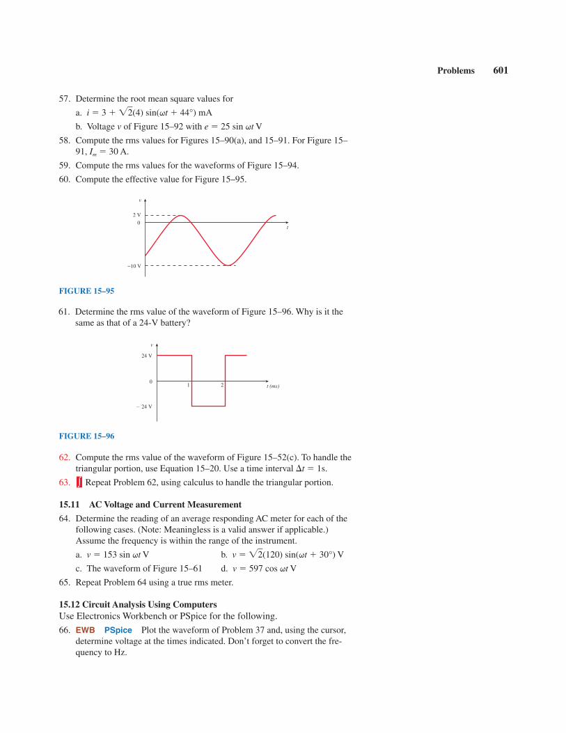
Problems 601
FIGURE 15–95
t
v
2 V
0
−10 V
FIGURE 15–96
t (ms)
v
24 V
01 2
24 V
62. Compute the rms value of the waveform of Figure 15–52(c). To handle thetriangular portion, use Equation 15–20. Use a time interval t 1s.
63. Repeat Problem 62, using calculus to handle the triangular portion.
15.11 AC Voltage and Current Measurement
64. Determine the reading of an average responding AC meter for each of thefollowing cases. (Note: Meaningless is a valid answer if applicable.)Assume the frequency is within the range of the instrument.
a. v 153 sin qt V b. v 2(120) sin(qt 30°) V
c. The waveform of Figure 15–61 d. v 597 cos qt V
65. Repeat Problem 64 using a true rms meter.
15.12 Circuit Analysis Using ComputersUse Electronics Workbench or PSpice for the following.
66. EWB PSpice Plot the waveform of Problem 37 and, using the cursor,determine voltage at the times indicated. Don’t forget to convert the fre-quency to Hz.
∫
57. Determine the root mean square values for
a. i 3 2(4) sin(qt 44°) mA
b. Voltage v of Figure 15–92 with e 25 sin qt V
58. Compute the rms values for Figures 15–90(a), and 15–91. For Figure 15–91, Im 30 A.
59. Compute the rms values for the waveforms of Figure 15–94.
60. Compute the effective value for Figure 15–95.
61. Determine the rms value of the waveform of Figure 15–96. Why is it thesame as that of a 24-V battery?

67. EWB PSpice Plot the waveform of Problem 41. Using the cursor, deter-mine the time at which v reaches 0 V. Don’t forget to convert the frequencyto Hz.
68. EWB PSpice Assume the equations of Problem 43 all represent volt-ages. For each case, plot the waveforms, then use the cursor to determinethe phase difference between waveforms.
602 Chapter 15 AC Fundamentals
In-Process Learning Check 1
1. 16.7 ms
2. Frequency doubles, period halves
3. 50 Hz; 20 ms
4. 20 V; 0.5 ms and 2.5 ms; 35 V: 4 ms and 5 ms
5. (c) and (d); Since current is directly proportional to the voltage, it will havethe same waveshape.
6. 250 Hz
7. f1 100 Hz; f2 33.3 Hz
8. 50 kHz and 1 MHz
9. 22.5 Hz
10. At 12 ms, direction →; at 37 ms, direction ←; at 60 ms, →11. At 75 ms, i 5 A
In-Process Learning Check 2
1.
2. a. 0.349 b. 0.873
c. 2.09 d. 4.36
3. 30°; 120°; 450°
4. Same as Figure 15–27 with T 10 s and amplitude 50 mA.
5. 1.508 106 rad/s
6. i 8 sin 157t A
7. i 6 sin 69.81t A
8. a. i 250 sin(251t 30°) A
b. i 20 sin(62.8t 45°) A
c. v 40 sin(628t 30°) V
d. v 80 sin(314 103t 36°) V
9. a. 2.95 ms; 7.05 ms; 22.95 ms; 27.05 ms
b. 11.67 ms; 18.33 ms; 31.67 ms; 38.33 ms
ANSWERS TO IN-PROCESSLEARNING CHECKS
a (deg) 0 45 90 135 180 225 270 315 360i (mA) 0 10.6 15 10.6 0 10.6 15 10.6 0
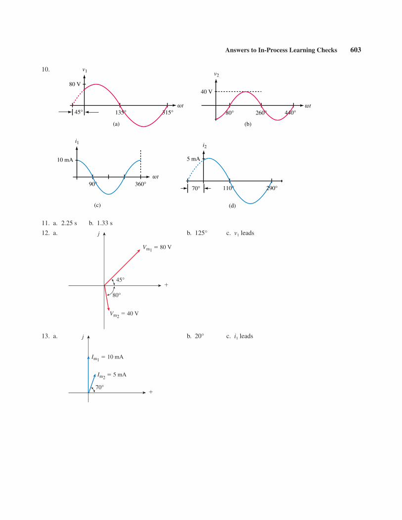
10.
Answers to In-Process Learning Checks 603
(a)
ωt
v1
80 V
45° 135° 315°
(b)
ωt
v2
40 V
440°80° 260°
(c)
i1
360°90°ωt
10 mA
70°
(d)
i2
5 mA
290°110°
11. a. 2.25 s b. 1.33 s
12. a. b. 125° c. v1 leads
13. a. b. 20° c. i1 leads
80°
45°
j
Vm1 80 V
Vm2 40 V
70°
j
Im1 10 mA
Im2 5 mA

OBJECTIVES
After studying this chapter, you will beable to
• express complex numbers in rectangularand polar forms,
• represent ac voltage and current phasorsas complex numbers,
• represent voltage and current sources intransformed form,
• add and subtract currents and voltagesusing phasors,
• compute inductive and capacitive reac-tance,
• determine voltages and currents in sim-ple ac circuits,
• explain the impedance concept,
• determine impedance for R, L, and Ccircuit elements,
• determine voltages and currents in sim-ple ac circuits using the impedance con-cept,
• use Electronics Workbench and PSpiceto solve simple ac circuit problems.
KEY TERMS
Capacitive Reactance
Complex Number
Impedance
Inductive Reactance
j 1Phasor Domain
Polar Form
Rectangular Form
Time Domain
OUTLINE
Complex Number Review
Complex Numbers in AC Analysis
R, L, and C Circuits with Sinusoidal Excitation
Resistance and Sinusoidal AC
Inductance and Sinusoidal AC
Capacitance and Sinusoidal AC
The Impedance Concept
Computer Analysis of AC Circuits
R, L, and C Elements andthe Impedance Concept16

In Chapter 15, you learned how to analyze a few simple ac circuits in the timedomain using voltages and currents expressed as functions of time. However,
this is not a very practical approach. A more practical approach is to represent acvoltages and currents as phasors, circuit elements as impedances, and analyzecircuits in the phasor domain using complex algebra. With this approach, ac cir-cuit analysis is handled much like dc circuit analysis, and all basic relationshipsand theorems—Ohm’s law, Kirchhoff’s laws, mesh and nodal analysis, superpo-sition and so on—apply. The major difference is that ac quantities are complexrather than real as with dc. While this complicates computational details, it doesnot alter basic circuit principles. This is the approach used in practice. The basicideas are developed in this chapter.
Since phasor analysis and the impedance concept require a familiarity withcomplex numbers, we begin with a short review.
605
CHAPTER PREVIEW
PUTTING IT INPERSPECTIVE
Charles Proteus Steinmetz
CHARLES STEINMETZ WAS BORN IN Breslau, Germany in 1865 and emigrated tothe United States in 1889. In 1892, he began working for the General ElectricCompany in Schenectady, New York, where he stayed until his death in 1923,and it was there that his work revolutionized ac circuit analysis. Prior to his time,this analysis had to be carried out using calculus, a difficult and time-consumingprocess. By 1893, however, Steinmetz had reduced the very complex alternating-current theory to, in his words, “a simple problem in algebra.” The key conceptin this simplification was the phasor—a representation based on complex num-bers. By representing voltages and currents as phasors, Steinmetz was able todefine a quantity called impedance and then use it to determine voltage and cur-rent magnitude and phase relationships in one algebraic operation.
Steinmetz wrote the seminal textbook on ac analysis based on his method,but at the time he introduced it he was practically the only person who under-stood it. Now, however, it is common knowledge and one of the basic tools ofthe electrical engineer and technologist. In this chapter, we learn the method andillustrate its application to the solution of basic ac circuit problems.
In addition to his work for GE, Charles Steinmetz was a professor of electri-cal engineering (1902–1913) and electrophysics (1913–1923) at Union Univer-sity (now Union College) in Schenectady.

16.1 Complex Number ReviewA complex number is a number of the form C a jb, where a and b arereal numbers and j 1. The number a is called the real part of C and bis called its imaginary part. (In circuit theory, j is used to denote the imagi-nary component rather than i to avoid confusion with current i.)
Geometrical RepresentationComplex numbers may be represented geometrically, either in rectangularform or in polar form as points on a two-dimensional plane called the com-plex plane (Figure 16–1). The complex number C 6 j8, for example,represents a point whose coordinate on the real axis is 6 and whose coordi-nate on the imaginary axis is 8. This form of representation is called the rec-tangular form.
Complex numbers may also be represented in polar form by magnitudeand angle. Thus, C 10∠53.13° (Figure 16–2) is a complex number withmagnitude 10 and angle 53.13°. This magnitude and angle representation isjust an alternate way of specifying the location of the point represented byC a jb.
Conversion between Rectangular and Polar FormsTo convert between forms, note from Figure 16–3 that
C a jb (rectangular form) (16–1)
C C∠v (polar form) (16–2)
where C is the magnitude of C. From the geometry of the triangle,
a C cos v (16–3a)
b C sin v (16–3b)
where
C a2 b2 (16–4a)
and
v tan1ba
(16–4b)
Equations 16–3 and 16–4 permit conversion between forms. When usingEquation 16–4b, however, be careful when the number to be converted is inthe second or third quadrant, as the angle obtained is the supplementaryangle rather than the actual angle in these two quadrants. This is illustratedin Example 16–1 for the complex number W.
606 Chapter 16 R, L, and C Elements and the Impedance Concept
FIGURE 16–1 A complex number inrectangular form.
j
j
20
2
4
6
8
4 8 10 Real
Axis6
Imag
inar
y A
xis
C = 6 j8
j
Real Axis
C = 10∠53.13°
10
53.13°
FIGURE 16–2 A complex num-ber in polar form.
j
Real Axis
C = a jb = C∠θ
θ
C
a
b
FIGURE 16–3 Polar and rectan-gular equivalence.
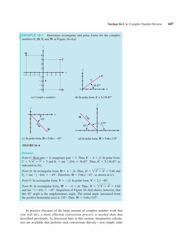
EXAMPLE 16–1 Determine rectangular and polar forms for the complexnumbers C, D, V, and W of Figure 16–4(a)
In practice (because of the large amount of complex number work thatyou will do), a more efficient conversion process is needed than thatdescribed previously. As discussed later in this section, inexpensive calcula-tors are available that perform such conversions directly—you simply enter
Section 16.1 Complex Number Review 607
SolutionPoint C: Real part 4; imaginary part 3. Thus, C 4 j3. In polar form,C 42 32 5 and vC tan1 (3/4) 36.87°. Thus, C 5∠36.87° asindicated in (b).
Point D: In rectangular form, D 4 j4. Thus, D 42 42 5.66 andvD tan1 (4/4) 45°. Therefore, D 5.66∠45°, as shown in (c).
Point V: In rectangular form, V j2. In polar form, V 2∠90°.
Point W: In rectangular form, W 4 j4. Thus, W 42 42 5.66and tan1 (4/4) 45°. Inspection of Figure 16–4(d) shows, however, thatthis 45° angle is the supplementary angle. The actual angle (measured fromthe positive horizontal axis) is 135°. Thus, W 5.66∠135°.
j
112341
1
2
3
4
2 4
4
3
2
3
W
C
D
V
(a) Complex numbers
j
C
(b) In polar form, C = 5∠36.87°
36.87°
5
j
D
(c) In polar form, D = 5.66∠45°
45°5.66
j
W
(d) In polar form, W = 5.66∠135°
135°
5.66
45°
FIGURE 16–4

the complex number components and press the conversion key. With these,the problem of determining angles for numbers such as W in Example 16–1does not occur; you just enter 4 j4 and the calculator returns 5.66∠135°.
Powers of jPowers of j are frequently required in calculations. Here are some usefulpowers:
j2 (1)(1) 1
j3 j2j j
j4 j2j2 (1) (1) 1 (16–5)
(j)j 1
1j
1j
jj
jj2 j
Addition and Subtraction of Complex NumbersAddition and subtraction of complex numbers can be performed analyticallyor graphically. Analytic addition and subtraction is most easily illustrated inrectangular form, while graphical addition and subtraction is best illustratedin polar form. For analytic addition, add real and imaginary parts separately.Similarly for subtraction. For graphical addition, add vectorially as in Figure16–5(a); for subtraction, change the sign of the subtrahend, then add, as inFigure 16–5(b).
608 Chapter 16 R, L, and C Elements and the Impedance Concept
EXAMPLE 16–2 Given A 2 j1 and B 1 j3. Determine their sumand difference analytically and graphically.
SolutionA B (2 j1) (1 j3) (2 1) j(1 3) 3 j4.
A B (2 j1) (1 j3) (2 1) j(1 3) 1 j2.
Graphical addition and subtraction are shown in Figure 16–5.
j
1
1
2
3
4
2 4
3
B
A
(a)
A B = 3 j4
j
1
1
2
3
2 4
3
B
B
A
(b)
A (B) = A B = 1 j2
FIGURE 16–5

Multiplication and Division of Complex NumbersThese operations are usually performed in polar form. For multiplication,multiply magnitudes and add angles algebraically. For division, divide themagnitude of the denominator into the magnitude of the numerator, thensubtract algebraically the angle of the denominator from that of the numera-tor. Thus, given A A∠vA and B B∠vB,
A B ABvA vB (16–6)
A/B A/BvA vB (16–7)
Section 16.1 Complex Number Review 609
EXAMPLE 16–3 Given A 3∠35° and B 2∠20°, determine theproduct A B and the quotient A/B.
SolutionA B (3∠35°)(2∠20°) (3)(2)35° 20° 6∠15°
AB
(2(3∠∠
3250°)°)
32
35° (20°) 1.5∠55°
EXAMPLE 16–4 For computations involving purely real, purely imagi-nary, or small integer numbers, it is sometimes easier to multiply directly inrectangular form than it is to convert to polar. Compute the followingdirectly:
a. (j3)(2 j4).
b. (2 j3)(1 j5).
Solutiona. (j3)(2 j4) (j3)(2) (j3)( j4) j6 j212 12 j6
b. (2 j3)(1 j5) (2)(1) (2)( j5) ( j3)(1) ( j3)( j5) 2 j10 j3 j215 2 j13 15 13 j13
PRACTICEPROBLEMS 1
1. Polar numbers with the same angle can be added or subtracted directly with-out conversion to rectangular form. For example, the sum of 6 ∠36.87° and4 ∠36.87° is 10 ∠36.87°, while the difference is 6 ∠36.87° 4 ∠36.87° 2 ∠36.87°. By means of sketches, indicate why this procedure is valid.
2. To compare methods of multiplication with small integer values, convert thenumbers of Example 16–4 to polar form, multiply them, then convert theanswers back to rectangular form.
Answers:1. Since the numbers have the same angle, their sum also has the same angle and thus,
their magnitudes simply add (or subtract).

ReciprocalsThe reciprocal of a complex number C C∠v is
C
1∠v
C1
∠v (16–8)
Thus,
20∠
130° 0.05∠30°
Complex ConjugatesThe conjugate of a complex number (denoted by an asterisk *) is a complexnumber with the same real part but the opposite imaginary part. Thus, theconjugate of C C∠v a jb is C* C∠v a jb. For example, ifC 3 j4 5∠53.13°, then C* 3 j4 5∠53.13°.
Calculators for AC AnalysisThe analysis of ac circuits involves a considerable amount of complexnumber arithmetic; thus, you will need a calculator that can work easilywith complex numbers. There are several inexpensive calculators on themarket that are suitable for this purpose in that they can perform allrequired calculations (addition, subtraction, multiplication, and division) ineither rectangular or polar form without the need for conversion. This isimportant, because it saves you a great deal of time and cuts down onerrors. To illustrate, consider Example 16–5. Using a calculator with onlybasic complex number conversion capabilities requires that you convertbetween forms as illustrated. On the other hand, a calculator with moresophisticated complex number capabilities (such as that shown in Figure16–6) allows you to perform the calculation without going through all theintermediate conversion steps. You need to acquire an appropriate calculatorand learn to use it proficiently.
610 Chapter 16 R, L, and C Elements and the Impedance Concept
EXAMPLE 16–5 The following illustrates the type of calculations that youwill encounter. Use your calculator to reduce the following to rectangularform:
(6 j5) (36
j340)∠(1
503∠.1430°°)
Solution Using a calculator with basic capabilities requires a number ofintermediate steps, some of which are shown below.
answer (6 j5)
(6 j5) (5∠53.13)(10∠40)
24 j24
(5∠53.13)(10∠40)
6 (18 j24)
FIGURE 16–6 This calculator dis-plays complex numbers in standardmathematical notation.

16.2 Complex Numbers in AC Analysis
Representing AC Voltages and Currents by Complex NumbersAs you learned in Chapter 15, ac voltages and currents can be represented asphasors. Since phasors have magnitude and angle, they can be viewed ascomplex numbers. To get at the idea, consider the voltage source of Figure16–7(a). Its phasor equivalent (b) has magnitude Em and angle v. It thereforecan be viewed as the complex number
E Em∠v (16–9)
Section 16.2 Complex Numbers in AC Analysis 611
(6 j5)
(6 j5) 1.473∠58.13 (6 j5) (0.778 j1.251)
6.778 j3.749
Using a calculator such as that shown in Figure 16–6 saves steps, as it multi-plies (3 j4)(10∠40°) and adds 6 30∠53.13°, etc., directly, without yourhaving to convert forms.
(5∠53.13)(10∠40)
33.94∠45
e(t)
(a) e(t) = Em sin (ωt θ) (b) E = Em∠θ
E
θ
E m
j
FIGURE 16–7 Representation of a sinusoidal source voltage as a complex number.
From this point of view, the sinusoidal voltage e(t) 200 sin(qt 40°) ofFigure 16–8(a) and (b) can be represented by its phasor equivalent, E 200 V∠40°, as in (c).
(a) e = 200 sin (ωt 40°) V
e
(b) Waveform
ωt
200
e
40°
(c) Phasor equivalent
E = 200 V∠40°
40°200 V
j
FIGURE 16–8 Transforming e 200 sin(qt 40°) V to E 200 V∠40°.

We can take advantage of this equivalence. Rather than show a sourceas a time-varying voltage e(t) that we subsequently convert to a phasor, wecan represent the source by its phasor equivalent right from the start. Thisviewpoint is illustrated in Figure 16–9. Since E 200 V∠40°, this represen-tation retains all the original information of Figure 16–8 with the exceptionof the sinusoidal time variation. However, since the sinusoidal waveform andtime variation is implicit in the definition of a phasor, you can easily restorethis information if it is needed.
The idea illustrated in Figure 16–9 is of fundamental importance to cir-cuit theory. By replacing the time function e(t) with its phasor equivalent E,we have transformed the source from the time domain to the phasor domain.The value of this approach is illustrated next.
Before we move on, we should note that both Kirchhoff’s voltage lawand Kirchhoff’s current law apply in the time domain (i.e., when voltagesand currents are expressed as functions of time) and in the phasor domain(i.e., when voltages and currents are represented as phasors). For example,e v1 v2 in the time domain can be transformed to E V1 V2 in thephasor domain and vice versa. Similarly for currents.
Summing AC Voltages and CurrentsSinusoidal quantites must sometimes be added or subtracted as in Figure16–10. Here, we want the sum of e1 and e2, where e1 10 sin qt and e2 15 sin(qt 60°). The sum of e1 and e2 can be found by adding waveformspoint by point as in (b). For example, at qt 0°, e1 10 sin 0° 0 ande2 15 sin(0° 60°) 13 V, and their sum is 13 V. Similarly, at qt 90°,e1 10 sin 90° 10 V and e2 15 sin(90° 60°) 15 sin 150° 7.5,and their sum is 17.5 V. Continuing in this manner, the sum of e1 e2 (thegreen waveform) is obtained.
612 Chapter 16 R, L, and C Elements and the Impedance Concept
E = 200 V∠40°
Transformed source
FIGURE 16–9 Direct transformationof the source.
e2
e1
v (t)
(a) e1 = 10 sin ωte2 = 15 sin (ωt 60°)
17.5 V
13.0 V
(b) Waveforms
60°90°
ωt
e1 = 10 sin ωt
v = e1 e2
0
e2 = 15 sin (ωt 60°)
360°180° 270°
FIGURE 16–10 Summing waveforms point by point.
As you can see, the process is tedious and provides no analytic expres-sion for the resulting voltage. A better way is to transform the sources anduse complex numbers to perform the addition. This is shown in Figure 16–11.
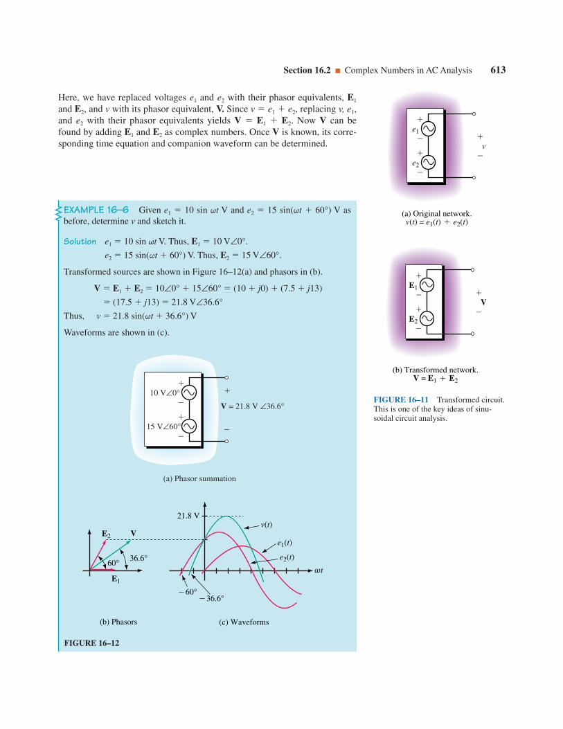
Here, we have replaced voltages e1 and e2 with their phasor equivalents, E1
and E2, and v with its phasor equivalent, V. Since v e1 e2, replacing v, e1,and e2 with their phasor equivalents yields V E1 E2. Now V can befound by adding E1 and E2 as complex numbers. Once V is known, its corre-sponding time equation and companion waveform can be determined.
Section 16.2 Complex Numbers in AC Analysis 613
e2
e1
v
(a) Original network.v(t) = e1(t) e2(t)
E2
E1
V
(b) Transformed network.V = E1 E2
FIGURE 16–11 Transformed circuit.This is one of the key ideas of sinu-soidal circuit analysis.
EXAMPLE 16–6 Given e1 10 sin qt V and e2 15 sin(qt 60°) V asbefore, determine v and sketch it.
Solution e1 10 sin qt V. Thus, E1 10 V∠0°.
e2 15 sin(qt 60°) V. Thus, E2 15 V∠60°.
Transformed sources are shown in Figure 16–12(a) and phasors in (b).
V E1 E2 10∠0° 15∠60° (10 j0) (7.5 j13)
(17.5 j13) 21.8 V∠36.6°
Thus, v 21.8 sin(qt 36.6°) V
Waveforms are shown in (c).
(a) Phasor summation
V = 21.8 V ∠36.6°
10 V∠0°
15 V∠60°
(c) Waveforms
60°
ωt
36.6°
e2(t)
e1(t)
v(t)21.8 V
(b) Phasors
VE2
E1
36.6°60°
FIGURE 16–12

614 Chapter 16 R, L, and C Elements and the Impedance Concept
PRACTICEPROBLEMS 2
Verify by direct substitution that v 21.8 sin(qt 36.6°) V, as in Figure 16–12,is the sum of e1 and e2. To do this, compute e1 and e2 at a point, add them, thencompare the sum to 21.8 sin(qt 36.6°) V computed at the same point. Performthis computation at qt 30° intervals over the complete cycle to satisfy yourselfthat the result is true everywhere. (For example, at qt 0°, v 21.8 sin(qt 36.6°) 21.8 sin(36.6°) 13 V, as we saw earlier in Figure 16–10.)
Answer: Here are the points on the graph at 30° intervals:
t 0° 30° 60° 90° 120° 150° 180° 210° 240° 270° 300° 330° 360°
v 13 20 21.7 17.5 8.66 2.5 13 20 21.7 17.5 8.66 2.5 13
IMPORTANT NOTES...1. To this point, we have used peak values such as Vm and Im to represent the
magnitudes of phasor voltages and currents, as this has been most conve-nient for our purposes. In practice, however, rms values are used instead.Accordingly, we will now change to rms. Thus, from here on, the phasor V 120 V ∠0° will be taken to mean a voltage of 120 volts rms at an angle of0°. If you need to convert this to a time function, first multiply the rmsvalue by 2, then follow the usual procedure. Thus, v 2 (120) sin qt 170 sin qt.
2. To add or subtract sinusoidal voltages or currents, follow the three stepsoutlined in Example 16–6. That is,
• convert sine waves to phasors and express them in complex numberform,
• add or subtract the complex numbers,
• convert back to time functions if desired.
3. Although we use phasors to represent sinusoidal waveforms, it should benoted that sine waves and phasors are not the same thing. Sinusoidal volt-ages and currents are real—they are the actual quantities that you measurewith meters and whose waveforms you see on oscilloscopes. Phasors, onthe other hand, are mathematical abstractions that we use to help visualizerelationships and solve problems.
4. Quantities expressed as time functions are said to be in the time domain,while quantities expressed as phasors are said to be in the phasor (or fre-quency) domain. Thus, e 170 sin qt V is in the time domain, while V 120 V ∠0° is in the phasor domain.

While it may seem silly to convert peak values to rms and then convertrms back to peak as we did here, we did it for a reason. The reason is that verysoon, we will stop working in the time domain entirely and work only withphasors. At that point, the solution will be complete when we have the answerin the form I 11.3∠41.4°. (To help focus on rms, voltages and currents inthe next two examples (and in other examples to come) are expressed as anrms value times 2.)
Section 16.2 Complex Numbers in AC Analysis 615
EXAMPLE 16–7 Express the voltages and currents of Figure 16–13 in boththe time and the phasor domains.
FIGURE 16–13
Solutiona. Time domain: v 100 sin(qt 80°) volts.
Phasor domain: V (0.707)(100 V ∠80°) 70.7 V∠80°.
b. Time domain: i 40 sin(qt 25°) mA.Phasor domain: I (0.707)(40 mA∠25°) 28.3 mA∠25°.
(a)
ωt
100
v (V)
80°
(b)
ωt
40 mA
i
25°
EXAMPLE 16–8 If i1 14.14 sin(qt 55°) A and i2 4 sin(qt 15°) A,determine their sum, i. Work with rms values.
SolutionI1 (0.707)(14.14 A)∠55° 10 A∠55°
I2 (0.707)(4 A)∠15° 2.828 A∠15°
I I1 I2 10 A∠55° 2.828 A∠15°
(5.74 A j8.19 A) (2.73 A j0.732 A)
8.47 A j7.46 A 11.3 A∠41.4
i(t) 2(11.3) sin(qt 41.4°) 16 sin(qt 41.4°) A

616 Chapter 16 R, L, and C Elements and the Impedance Concept
EXAMPLE 16–10 For Figure 16–15, i1 2(23) sin qt mA, i2 2(0.29)sin(qt 63°)A and i3 2(127) 103 sin(qt 72°)A. Determine current iT.
Solution Convert to phasors. Thus, I1 23 mA∠0°, I2 0.29 A∠63°, andI3 127 103 A∠72°. KCL yields IT I1 I2 I3 23 mA∠0° 290 mA∠63° 127 mA∠72° 238 mA∠35.4°. Converting back to afunction of time yields iT 2(238) sin(qt 35.4°) mA.
FIGURE 16–15
EXAMPLE 16–9 For Figure 16–14, v1 2(16) sin qt V, v2 2(24)sin(qt 90°) and v3 2(15) sin(qt 90°) V. Determine source voltage e.
Solution The answer can be obtained by KVL. First, convert to phasors. Thus,V1 16 V∠0°, V2 24 V∠90°, and V3 15 V∠90°. KVL yields E V1 V2 V3 16 V∠0° 24 V∠90° 15 V∠90° 18.4 V∠29.4°. Convert-ing back to a function of time yields e 2(18.4) sin(qt 29.4°) V.
FIGURE 16–14
v1
v3
e
v2
i1 i2iTi3
PRACTICEPROBLEMS 3
1. Convert the following to time functions. Values are rms.
a. E 500 mV∠20° b. I 80 A∠40°
2. For the circuit of Figure 16–16, determine voltage e1.
Answers:1. a. e 707 sin(qt 20°) mV b. i 113 sin(qt 40°) A
2. e1 221 sin(qt 99.8°) V
e1
e2 = 141.4 sin (ωt 30°) V
v = 170 sin (ωt 60°) V
FIGURE 16–16

16.3 R, L, and C Circuits with Sinusoidal ExcitationR, L, and C circuit elements each have quite different electrical properties.Resistance, for example, opposes current, while inductance opposes changes incurrent, and capacitance opposes changes in voltage. These differences resultin quite different voltage-current relationships as you saw earlier. We nowinvestigate these relationships for the case of sinusoidal ac. Sine waves haveseveral important characteristics that you will discover from this investigation:
1. When a circuit consisting of linear circuit elements R, L, and C is con-nected to a sinusoidal source, all currents and voltages in the circuit willbe sinusoidal.
2. These sine waves have the same frequency as the source and differ from itonly in terms of their magnitudes and phase angles.
16.4 Resistance and Sinusoidal ACWe begin with a purely resistive circuit. Here, Ohm’s law applies and thus,current is directly proportional to voltage. Current variations therefore fol-low voltage variations, reaching their peak when voltage reaches its peak,
Section 16.4 Resistance and Sinusoidal AC 617
IN-PROCESSLEARNINGCHECK 1
1. Convert the following to polar form:
a. j6 b. j4 c. 3 j3 d. 4 j6
e. 5 j8 f. 1 j2 g. 2 j3
2. Convert the following to rectangular form:
a. 4∠90° b. 3∠0° c. 2∠90° d. 5∠40°
e. 6∠120° f. 2.5∠20° g. 1.75∠160°
3. If C 12∠140°, what is C?
4. Given: C1 36 j4 and C2 52 j11. Determine C1 C2 and C1 C2.Express in rectangular form.
5. Given: C1 24∠25° and C2 12∠125°. Determine C1 C2 and C1/C2.
6. Compute the following and express answers in rectangular form:
a. 160∠
2j04°
(14 j2) b. (1 j6) 2 7. For Figure 16–17, determine iT where i1 10 sin qt, i2 20 sin(qt 90°),
and i3 5 sin(qt 90°).
(12∠0°)(14 j2)6 (10∠20°)(2∠10°)
(Answers are at the end of the chapter.)
FIGURE 16–17
i1
iT = i1 i2 i3
i2 i3

changing direction when voltage changes polarity, and so on (Figure 16–18).From this, we conclude that for a purely resistive circuit, current and voltageare in phase. Since voltage and current waveforms coincide, their phasorsalso coincide (Figure 16–19).
618 Chapter 16 R, L, and C Elements and the Impedance Concept
(a) Source voltage is a sine wave.Therefore, vR is a sine wave.
e iR
vR
(b) iR = vR/R. ThereforeiR is a sine wave.
t
vR
iR
FIGURE 16–18 Ohm’s law applies to resistors. Note that current and voltage are inphase.
j
VR
VR
IR
IR
FIGURE 16–19 For a resistor, volt-age and current phasors are in phase.
The relationship illustrated in Figure 16–18 may be stated mathemati-cally as
iR v
RR
Vm s
R
in qt
V
Rmsin qt Im sin qt (16–10)
where
Im Vm/R (16–11)
Transposing,
Vm ImR (16–12)
The in-phase relationship is true regardless of reference. Thus, if vR Vm sin(qt v), then iR Im sin(qt v).
EXAMPLE 16–11 For the circuit of Figure 16–18(a), if R 5 and iR 12 sin(qt 18) A, determine vR.
Solution vR RiR 5 12 sin(qt 18°) 60 sin(qt 18°) V. Thewaveforms are shown in Figure 16–20.
ωt
60 V
12 A
2
232
vR
iR
18°FIGURE 16–20

16.5 Inductance and Sinusoidal AC
Phase Lag in an Inductive CircuitAs you saw in Chapter 13, for an ideal inductor, voltage vL is proportional tothe rate of change of current. Because of this, voltage and current are not inphase as they are for a resistive circuit. This can be shown with a bit of cal-culus. From Figure 16–21, vL LdiL/dt. For a sine wave of current, you getwhen you differentiate
vL LdditL L
ddt(Im sin qt) qLIm cos qt Vm cos qt
Utilizing the trigonometric identity cos qt sin(qt 90°), you can writethis as
vL Vm sin(qt 90°) (16–13)
where
Vm qLIm (16–14)
Voltage and current waveforms are shown in Figure 16–22, and phasors inFigure 16–23. As you can see, for a purely inductive circuit, current lagsvoltage by 90° (i.e., 1⁄4 cycle). Alternatively you can say that voltage leadscurrent by 90°.
Section 16.5 Inductance and Sinusoidal AC 619
PRACTICEPROBLEMS 4
1. If vR 150 cos qt V and R 25 k, determine iR and sketch both wave-forms.
2. If vR 100 sin(qt 30°) V and R 0.2 M, determine iR and sketch bothwaveforms.
Answers:1. iR 6 cos qt mA. vR and iR are in phase.
2. iR 0.5 sin(qt 30°) mA. vR and iR are in phase.
iL
vL = L
L
diLdt
FIGURE 16–21 Voltage vL is propor-tional to the rate of change of current iL.
ωt
VmIm iL
vL
π2
π
2 π
3 π2
j
VL
ILFIGURE 16–22 For inductance, current lags voltage by 90°. Here iL is reference.
FIGURE 16–23 Phasors for thewaveforms of Fig. 16–22 showing the90° lag of current.
Although we have shown that current lags voltage by 90° for the case ofFigure 16–22, this relationship is true in general, that is, current always lagsvoltage by 90° regardless of the choice of reference. This is illustrated inFigure 16–24. Here, VL is at 0° and IL at 90°. Thus, voltage vL will be asine wave and current iL a negative cosine wave, i.e., iL Im cos qt. Since

iL is a negative cosine wave, it can also be expressed as iL Im sin(qt 90°).The waveforms are shown in (b).
Since current always lags voltage by 90° for a pure inductance, you can,if you know the phase of the voltage, determine the phase of the current, andvice versa. Thus, if vL is known, iL must lag it by 90°, while if iL is known, vL
must lead it by 90°.
Inductive ReactanceFrom Equation 16–14, we see that the ratio Vm to Im is
V
Im
m qL (16–15)
This ratio is defined as inductive reactance and is given the symbol XL.Since the ratio of volts to amps is ohms, reactance has units of ohms.Thus,
XL V
Im
m () (16–16)
Combining Equations 16–15 and 16–16 yields
XL qL () (16–17)
where q is in radians per second and L is in henries. Reactance XL repre-sents the opposition that inductance presents to current for the sinusoidalac case.
We now have everything that we need to solve simple inductive circuitswith sinusoidal excitation, that is, we know that current lags voltage by 90°and that their amplitudes are related by
Im V
Xm
L
(16–18)
and
Vm ImXL (16–19)
620 Chapter 16 R, L, and C Elements and the Impedance Concept
(b) Waveforms
0ωt
iL
vL
(a) Current IL always lagsvoltage VL by 90°
j
IL
VL
Vm
Im
2
2
32
FIGURE 16–24 Phasors and wave-forms when VL is used as reference.
EXAMPLE 16–12 The voltage across a 0.2-H inductance is vL 100 sin(400t 70°) V. Determine iL and sketch it.
Solution q 400 rad/s. Therefore, XL qL (400)(0.2) 80 .
Im V
Xm
L
18000V
1.25 A
The current lags the voltage by 90°. Therefore iL 1.25 sin(400t 20°) A asindicated in Figure 16–25.

Section 16.5 Inductance and Sinusoidal AC 621
FIGURE 16–25 With voltage VL at 70°, current IL will be 90° later at 20°.
j
VL = 70.7 V∠70°
IL = 0.884 A∠20°
20°
70°
(a) (b)
ωt
vL = 100 sin (400t 70°)V
iL = 1.25 sin (400t 20°)A
100 V
1.25 A
2
232
70°
90°
20°
EXAMPLE 16–13 The current through a 0.01-H inductance is iL 20sin(qt 50°) A and f 60 Hz. Determine vL.
Solutionq 2pf 2p(60) 377 rad/s
XL qL (377)(0.01) 3.77
Vm ImXL (20 A)(3.77 ) 75.4 V
Voltage leads current by 90°. Thus, vL 75.4 sin(377t 40°) V as shown inFigure 16–26.
FIGURE 16–26
(a)
j
VL = 53.3 V 40°
IL = 14.1 A 50°
50°
40°
(b)
ωt
vL = 75.4 sin (ωt 40°)
iL = 20 sin (ωt 50°)
75.4 V
20 A
2
232
40°
50°90°
PRACTICEPROBLEMS 5
1. Two inductances are connected in series (Figure 16–27). If e 100 sin qtand f 10 kHz, determine the current. Sketch voltage and current wave-forms.
e(t) iL
0.2 H
0.6 HFIGURE 16–27
Remember to show phasors asrms values from now on.
NOTE…

Variation of Inductive Reactance with FrequencySince XL qL 2pfL, inductive reactance is directly proportional to fre-quency (Figure 16–28). Thus, if frequency is doubled, reactance doubles,while if frequency is halved, reactance halves, and so on. In addition, XL isdirectly proportional to inductance. Thus, if inductance is doubled, XL isdoubled, and so on. Note also that at f 0, XL 0 . This means thatinductance looks like a short circuit to dc. (We already concluded this earlierin Chapter 13.)
622 Chapter 16 R, L, and C Elements and the Impedance Concept
2. The current through a 0.5-H inductance is iL 100 sin(2400t 45°) mA.Determine vL and sketch voltage and current phasors and waveforms.
Answers:1. iL 1.99 sin(qt 90°) mA. Waveforms same as Figure 16–24.
2. vL 120 sin(2400t 135° V). See following art for waveforms.
ωtπ245° π 2 π3 π
2
vL
135°
iL
45°135°
j
VL IL
XL ()
1000
1500
3000
4500
6000
200 400 500f (Hz)
7500
300
L2 L1
FIGURE 16–28 Variation of XL with frequency. Note that L2 L1.
PRACTICEPROBLEMS 6
A circuit has 50 ohms inductive reactance. If both the inductance and the fre-quency are doubled, what is the new XL?
Answer: 200
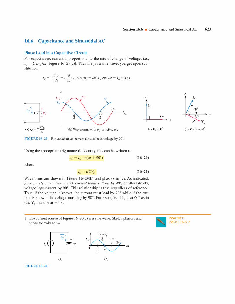
16.6 Capacitance and Sinusoidal AC
Phase Lead in a Capacitive CircuitFor capacitance, current is proportional to the rate of change of voltage, i.e.,iC C dvC /dt [Figure 16–29(a)]. Thus if vC is a sine wave, you get upon sub-stitution
iC Cd
d
v
tC
Cddt(Vm sin qt) qCVm cos qt Im cos qt
Section 16.6 Capacitance and Sinusoidal AC 623
ωt
VmIm
π2
π
2 π
3 π2
vC iC
(b) Waveforms with vC as reference
FIGURE 16–29 For capacitance, current always leads voltage by 90°.
Using the appropriate trigonometric identity, this can be written as
iC Im sin(qt 90°) (16–20)
where
Im qCVm (16–21)
Waveforms are shown in Figure 16–29(b) and phasors in (c). As indicated,for a purely capacitive circuit, current leads voltage by 90°, or alternatively,voltage lags current by 90°. This relationship is true regardless of reference.Thus, if the voltage is known, the current must lead by 90° while if the cur-rent is known, the voltage must lag by 90°. For example, if IC is at 60° as in(d), VC must be at 30°.
PRACTICEPROBLEMS 7
1. The current source of Figure 16–30(a) is a sine wave. Sketch phasors andcapacitor voltage vC.
FIGURE 16–30
(a)
iC
vCig
(b)
ωt
Im
2
0
232
iC = ig
(a) iC = C
iC vC
C
dvC
dt(c) Ve at 0º
j
IC
VC
(d) VC at −30º
j
IC
VC
30º
60º

Capacitive ReactanceNow consider the relationship between maximum capacitor voltage and cur-rent magnitudes. As we saw in Equation 16–21, they are related by Im qCVm. Rearranging, we get Vm/Im 1/qC. The ratio of Vm to Im is defined ascapacitive reactance and is given the symbol XC. That is,
XC V
Im
m ()
Since Vm/Im 1/qC, we also get
XC q
1C () (16–22)
where q is in radians per second and C is in farads. Reactance XC representsthe opposition that capacitance presents to current for the sinusoidal accase.
We now have everything that we need to solve simple capacitive circuitswith sinusoidal excitation, i.e., we know that current leads voltage by 90°and that
Im V
Xm
C
(16–23)
and
Vm ImXC (16–24)
624 Chapter 16 R, L, and C Elements and the Impedance Concept
2. Refer to the circuit of Figure 16–31(a):
a. Sketch the phasors.
b. Sketch capacitor current iC.
Answers:1. IC is at 0°; VC is at 90°; vC is a negative cosine wave.
2. a. VC is at 45° and IC is at 135°.
b. Waveforms are the same as for Problem 2, Practice Problem 5, except that voltageand current waveforms are interchanged.
(a)
e iC
(b)
ωt
Em
45°
e
FIGURE 16–31

Section 16.6 Capacitance and Sinusoidal AC 625
EXAMPLE 16–14 The voltage across a 10-mF capacitance is vC 100sin(qt 40°) V and f 1000 Hz. Determine iC and sketch its waveform.
Solutionq 2pf 2p(1000 Hz) 6283 rad/s
XC q
1C
(6283)(110 106) 15.92
Im V
Xm
C
1150.902V
6.28 A
Since current leads voltage by 90°, iC 6.28 sin(6283t 50°) A as indicatedin Figure 16–32.
(a)
j
IC
VC
40°
50°
(b)
ωt
vC
iC
100 V
6.28 A
32
2
50°
40°
2
FIGURE 16–32 Phasors are not to scale with waveform.
EXAMPLE 16–15 The current through a 0.1-mF capacitance is iC 5sin(1000t 120°) mA. Determine vC.
Solution
XC q
1C 10 k
Thus, Vm ImXC (5 mA)(10 k) 50 V. Since voltage lags current by90°, vC 50 sin(1000t 30°) V. Waveforms and phasors are shown in Figure16–33.
1(1000 rad/s)(0.1 106 F)
(a)
j
ICVC
30°120°
(b)
ωt
vC
iC
50 V
5 mA
120°30°
FIGURE 16–33 Phasors are not to scale with waveform.

Variation of Capacitive Reactance with FrequencySince XC 1/qC 1/2pfC, the opposition that capacitance presents variesinversely with frequency. This means that the higher the frequency, the lowerthe reactance, and vice versa (Figure 16–35). At f 0 (i.e., dc), capacitivereactance is infinite. This means that a capacitance looks like an open circuitto dc. (We already concluded this earlier in Chapter 10.) Note that XC is alsoinversely proportional to capacitance. Thus, if capacitance is doubled, XC ishalved, and so on.
626 Chapter 16 R, L, and C Elements and the Impedance Concept
PRACTICEPROBLEMS 8
Two capacitances are connected in parallel (Figure 16–34). If e 100 sin qt Vand f 10 Hz, determine the source current. Sketch current and voltage phasorsand waveforms.
Answer: i 0.942 sin(62.8t 90°) 0.942 cos 62.8t ASee Figure 16–29(b) and (c).
FIGURE 16–34
e(t)
i
100 F 50 F
1. For a pure resistance, vR 100 sin(qt 30°) V. If R 2 , what is theexpression for iR?
2. For a pure inductance, vL 100 sin(qt 30°) V. If XL 2 , what is theexpression for iL?
3. For a pure capacitance, vC 100 sin(qt 30°) V. If XC 2 , what is theexpression for iC?
4. If f 100 Hz and XL 400 , what is L?
5. If f 100 Hz and XC 400 , what is C?
6. For each of the phasor sets of Figure 16–36, identify whether the circuit isresistive, inductive, or capacitive. Justify your answers.
IN-PROCESSLEARNINGCHECK 2
XC ()
10
1000
2000
30003183
637 797
1061 1591
2 4 5 f (kHz)3
FIGURE 16–35 XC varies inversely with frequency. Values shown are for C 0.05 mF.

Section 16.7 The Impedance Concept 627
(Answers are at the end of the chapter.)
(a)
V
I
j
(b)
j
IV
(c)
j
I
V
(d)
j
I
V
FIGURE 16–36
FIGURE 16–37 Impedance concept.
Z = ohmsVI
Z V
I
Although Z is a complex num-ber, it is not a phasor since itdoes not represent a sinusoidallyvarying quantity.
NOTES...
16.7 The Impedance ConceptIn Sections 16.5 and 16.6, we handled magnitude and phase analysis sepa-rately. However, this is not the way it is done in practice. In practice, we rep-resent circuit elements by their impedance, and determine magnitude andphase relationships in one step. Before we do this, however, we need to learnhow to represent circuit elements as impedances.
ImpedanceThe opposition that a circuit element presents to current in the phasordomain is defined as its impedance. The impedance of the element of Figure16–37, for example, is the ratio of its voltage phasor to its current phasor.Impedance is denoted by the boldface, uppercase letter Z. Thus,
Z VI (ohms) (16–25)
(This equation is sometimes referred to as Ohm’s law for ac circuits.)Since phasor voltages and currents are complex, Z is also complex. That
is,
Z VI
VI∠v (16–26)
where V and I are the rms magnitudes of V and I respectively, and v is theangle between them. From Equation 16–26,
Z Z∠v (16–27)
where Z V/I. Since V 0.707Vm and I 0.707Im, Z can also be expressedas Vm/Im. Once the impedance of a circuit is known, the current and voltagecan be determined using
I VZ
(16–28)
and
V IZ (16–29)
Let us now determine impedance for the basic circuit elements R, L, and C.

Resistance
For a pure resistance (Figure 16–38), voltage and current are in phase. Thus,if voltage has an angle v, current will have the same angle. For example, ifVR VR∠v, then I I∠v. Substituting into Equation 16–25 yields:
ZR VI
R
V
IR
∠∠v
v
V
IR∠0° R
Thus the impedance of a resistor is just its resistance. That is,
ZR R (16–30)
This agrees with what we know about resistive circuits, i.e., that the ratio ofvoltage to current is R, and that the angle between them is 0°.
Inductance
For a pure inductance, current lags voltage by 90°. Assuming a 0° angle forvoltage (we can assume any reference we want because we are interestedonly in the angle between VL and I), we can write VL VL∠0° and I I∠90°. The impedance of a pure inductance (Figure 16–39) is therefore
ZL VI
L
I∠VL
∠9
0
0
°
°
V
IL∠90° qL∠90° jqL
where we have used the fact that VL/IL qL. Thus,
ZL jqL jXL (16–31)
since qL is equal to XL.
EXAMPLE 16–16 Consider again Example 16–12. Given vL 100sin(400t 70°) and L 0.2 H, determine iL using the impedance concept.
Solution See Figure 16–40.
VL 70.7 V∠70° and q 400 rad/s
ZL jqL j(400)(0.2) j80
IL VZL
L
70.7j8∠070°
7800.7∠∠9700°°
0.884 A∠20°
In the time domain, iL 2(0.884) sin(400t 20°) 1.25 sin(400t 20°)A, which agrees with our previous solution.
628 Chapter 16 R, L, and C Elements and the Impedance Concept
I
VR
(a) Voltageand current
(b) Impedance
ZR = R
FIGURE 16–38 Impedance of a pureresistance.
I
VL
(a) Voltageand current
+
−
(b) Impedance
ZL = jωL
FIGURE 16–39 Impedance of a pureinductance.
IL
VL = 70.7 V∠0°ZL = j80
FIGURE 16–40

Capacitance
For a pure capacitance, current leads voltage by 90°. Its impedance (Figure16–41) is therefore
ZC VI
C
V
I∠C∠
90
0
°
°
V
IC∠90°
q
1
C∠90° j
q
1
C (ohms)
Thus,
ZC jq
1C jXC (ohms) (16–32)
since 1/qC is equal to XC.
Section 16.7 The Impedance Concept 629
ZC = j 1ωC
FIGURE 16–41 Impedance of a purecapacitance.
EXAMPLE 16–17 Given vC 100 sin(qt 40°), f 1000 Hz, and C 10 mF,determine iC in Figure 16–42.
Solutionq 2pf 2p(1000 Hz) 6283 rads/s
VC 70.7 V∠40°
ZC jq
1C j6283 1
10 106 j15.92 .
IC VZC
C
70
.7j∠15
.9420°
1750..972∠∠
4900°°
4.442 A∠50°
In the time domain, iC 2(4.442) sin(6283t 50°) 6.28 sin(6283t 50°) A, which agrees with our previous solution, in Example 16–14.
IC
VC = 70.7 V∠40°ZC = j15.92
PRACTICEPROBLEMS 9
1. If IL 5 mA∠60°, L 2 mH, and f 10 kHz, what is VL?
2. A capacitor has a reactance of 50 at 1200 Hz. If vC 80 sin 800t V, whatis iC?
Answers:1. 628 mV∠30°
2. 0.170 sin(800t 90°) A
FIGURE 16–42
A Final NoteThe real power of the impedance method becomes apparent when you con-sider complex circuits with elements in series, parallel, and so on. This we do

later, beginning in Chapter 18. Before we do this, however, there are someideas on power that you need to know. These are considered in Chapter 17.
16.8 Computer Analysis of AC CircuitsIn Chapter 15, you saw how to represent sinusoidal waveforms using PSpiceand Electronics Workbench. Let us now apply these tools to the ideas of thischapter. To illustrate, recall that in Example 16–6, we summed voltages e1 10 sin qt V and e2 15 sin(qt 60°) V using phasor methods to obtaintheir sum v 21.8 sin(qt 36.6°) V. We will now verify this summationnumerically. Since the process is independent of frequency, let us choose f 500 Hz. This yields a period of 2 ms; thus, 1⁄2 cycle is 1 ms, 1⁄4 cycle (90°) is500 ms, 45° is 250 ms, etc.
Electronics WorkbenchAs noted in Chapter 15, Electronics Workbench requires that you enter rmsvalues for waveforms. Thus, to represent 10 sin qt V, enter (0.7071)(10 V) 7.071 V as its magnitude, and to represent 15 sin(qt 60°) V, enter 10.607 V.You must also enter its angle. Procedure: Create the circuit of Figure 16–43(a)on the screen. Set Source 1 to 7.071 V, 0 deg, and 500 Hz using the procedureof Chapter 15. Similarly, set Source 2 to 10.607 V, 60 deg, and 500 Hz. ClickAnalysis, Transient, set TSTOP to 0.002 (to run the solution out to 2 ms sothat you display a full cycle) and TMAX to 2e-06 (to avoid getting a choppywaveform.) Highlight Node 1 (to display e1) and click Add. Repeat for Node 2(to display v) Click Simulate. Following simulation, graphs e1 (the red curve,left-hand scale) and v (the blue curve, right-hand scale) appear. Expand theAnalysis Graph window to full screen, then click the cursor icon and drag acursor to 500 ms or as close as you can get it and read values. (You should getabout 10 V for e1 and 17.5 V for v.) Scale values from the graph at 200-msincrements and tabulate. Now replace the sources with a single source of 21.8
630 Chapter 16 R, L, and C Elements and the Impedance Concept
ELECTRONICSWORKBENCH
PSpice
FIGURE 16–43 Summing sinusoidal waveforms with Electronics Workbench.
(b) Waveforms e1 and v(a) The circuit

sin(qt 36.6°) V. (Don’t forget to convert to rms). Run a simulation. Theresulting graph should be identical to v (the blue curve) of Figure 16–43(b).
OrCAD PSpiceWith PSpice, you can plot all three waveforms of Fig. 16–10 simultaneously.Procedure: Create the circuit of Fig. 16–44 using source VSIN. Double clickSource 1 and select Parts in the Property Editor. Set VOFF to OV, VAMPL to10V, FREQ to 500Hz, and PHASE to 0deg. Click Apply, then close theProperty Editor. Set up source 2 similarly. Now place markers as shown(Note 2) so that PSpice will automatically create the plots. Click the NewSimulation Profile icon, choose Transient, set TSTOP to 2ms (to display afull cycle), set Maximum Step Size to 1us (to yield a smooth plot), thenclick OK. Run the simulation and the waveforms of Figure 16–45 should
Section 16.8 Computer Analysis of AC Circuits 631
FIGURE 16–44 Summing sinusoidal waveforms with PSpice. Source 2 is displayedusing a differential marker.
1. Make sure that the polaritiesof the sources are as indi-cated. (You will have torotate V2 three times to get itinto the position shown.)
2. To display V2, use differen-tial markers (indicated as and on the toolbar).
NOTES…
FIGURE 16–45 PSpice waveforms. Compare to Figure 16–10.

632 Chapter 16 R, L, and C Elements and the Impedance Concept
EXAMPLE 16–18 Compute and plot the reactance of a 12-F capacitorover the range 10 Hz to 1000 Hz.
Solution PSpice has no command to compute reactance; however, we cancalculate voltage and current over the desired frequency range, then plot theirratio. This gives reactance. Procedure: Create the circuit of Figure 16–46 onthe screen. (Use source VAC here as it is the source to use for phasor analy-ses—see Appendix A). Note its default of 0V. Double click the default value(not the symbol) and in the dialog box, enter 120V, then click OK. Click theNew Simulations Profile icon, enter fig 16-46 for a name and then in the dia-log box that opens, select AC Sweep/Noise. For the Start Frequency, key in10Hz; for the End Frequency, key 1kHz; set AC Sweep type to Logarithmic,select Decade and type 100 into the Pts/Decade (points per decade) box. Runthe simultation and a set of empty axes appears. Click Trace, Add Trace andin the dialog box, click V1(C1), press the / key on the keyboard, then clickI(C1) to yield the ratio V1(C1)/I(C1) (which is the capacitor’s reactance).Click OK and PSpice will compute and plot the capacitor’s reactance versusfrequency, Figure 16–47. Compare its shape to Figure 16–35. Use the cursorto scale some values off the screen and verify each point using XC 1/qC.
FIGURE 16–46 Circuit for plotting reactance.
appear. Using the cursor, scale voltages at 500 ms. You should get 10 V fore1, 7.5 V for e2 and 17.5 V for v. Read values at 200-ms intervals and tabulate.Now replace the sources of Figure 16–44 with a single source of 21.8 sin(qt 36.6°) V, run a simulation, scale values, and compare results. They shouldagree.
Another Example
PSpice makes it easy to study the response of circuits over a range of fre-quencies. This is illustrated in Example 16–18.

Phasor Analysis
As a last example, we will show how to use PSpice to perform phasoranalysis—i.e., to solve problems with voltages and currents expressed inphasor form. To illustrate, consider again Example 16–17. Recall, VC 70.7V∠40°, C 10 mF, and f 1000 Hz. Procedure: Create the circuit on thescreen (Figure 16–48) using source VAC and component IPRINT (Note 1).Double click the VAC symbol and in the Property Editor, set ACMAG to70.7V and ACPHASE to 40deg. (See Note 2). Double click IPRINT and inthe Property Editor, type yes into cells AC, MAG, and PHASE. Click Applyand close the editor. Click the New Simulation Profile icon, select ACSweep/Noise, Linear, set both Start Frequency and End Frequency to
Section 16.8 Computer Analysis of AC Circuits 633
FIGURE 16–47 Reactance for a 12-mF capacitor versus frequency.
FIGURE16–48 Phasor analysis using PSpice. Component IPRINT is a softwareammeter.
1. Component IPRINT is a soft-ware ammeter, found in theSPECIAL parts library. Inthis example, we configure itto display ac current in mag-nitude and phase angle for-mat. Make sure that it is con-nected as shown in Figure16–48, since if it is reversed,the phase angle of the mea-sured current will be in errorby 180°.
2. If you want to display thephase of the source voltageon the schematic as in Figure16–48, double click thesource symbol and in theProperty Editor, clickACPHASE, Display, thenselect Value Only.
3. The results displayed byIPRINT are expressed inexponential format. Thus, fre-quency (Figure 16–49) isshown as 1.000E03, whichis 1.000 103 1000 Hz,etc.
NOTES…
16.1 Complex Number Review
1. Convert each of the following to polar form:
a. 5 j12 b. 9 j6 c. 8 j15 d. 10 j4
2. Convert each of the following to rectangular form:
a. 6∠30° b. 14∠90° c. 16∠0° d. 6∠150°
e. 20∠140° f. 12∠30° g. 15∠150°
3. Plot each of the following on the complex plane:
a. 4 j6 b. j4 c. 6∠90° d. 10∠135°
4. Simplify the following using powers of j:
a. j(1 j1) b. (j)(2 j5) c. j[ j(1 j6)]
d. ( j4)(j2 4) e. (2 j3)(3 j4)
5. Add or subtract as indicated. Express your answer in rectangular form.
a. (4 j8) (3 j2) b. (4 j8) (3 j2)
c. (4.1 j7.6) 12∠20° d. 2.9∠25° 7.3∠5°
e. 9.2∠120° (2.6 j4.1)
6. Multiply or divide as indicated. Express your answer in polar form.
a. (37 j9.8)(3.6 j12.3) b. (41.9∠80°)(16 j2)
c. 1492.1
j1j84..68
d. 42
1.61.
2∠j13887°.5
634 Chapter 16 R, L, and C Elements and the Impedance Concept
FIGURE 16–49 Current for the circuit of Figure 16–48. I 4.442 A ∠50°.
PRACTICEPROBLEMS 10
Modify Example 16–18 to plot both capacitor current and reactance on the samegraph. You will need to add a second Y-axis for the capacitor current. (SeeAppendix A if you need help.)
PROBLEMS
1000Hz and Total Points to 1. Run the simulation. When the simulation win-dow opens, click View, Output File, then scroll until you find the answers(Figure 16–49 and Note 3). The first number is the frequency (1000 Hz), thesecond number (IM) is the magnitude of the current (4.442 A), and the third(IP) is its phase (50 degrees). Thus, IC 4.442 A∠50° as we determined ear-lier in Example 16–17.
7. Reduce each of the following to polar form:
a. 15 j6 b.
c.
16.2 Complex Numbers in AC Analysis
8. In the manner of Figure 16–9, represent each of the following as trans-formed sources.
a. e 100 sin(qt 30°) V b. e 15 sin(qt 20°) V
c. e 50 sin(qt 90°) V d. e 50 cos qt V
e. e 40 sin(qt 120°) V f. e 80 sin(qt 70°) V
9. Determine the sinusoidal equivalent for each of the transformed sources ofFigure 16–50.
10. Given: e1 10 sin(qt 30°) V and e2 15 sin(qt 20°) V. Determinetheir sum v e1 e2 in the manner of Example 16–6, i.e.,
a. Convert e1 and e2 to phasor form.
b. Determine V E1 E2.
c. Convert V to the time domain.
d. Sketch e1, e2, and v as per Figure 16–12.
11. Repeat Problem 10 for v e1 e2.
Note: For the remaining problems and throughout the remainder of thebook, express phasor quantities as rms values rather than as peak values.
12. Express the voltages and currents of Figure 16–51 as time domain and pha-sor domain quantities.
16 j17 21∠60°
418∠40° 18∠40°
7 j12
21∠20° j4136∠0° (1 j12) 11∠40°
18∠40° (12 j8)
11 j11
Problems 635
10 V∠30°
(a)
15 V∠10°
(b)
FIGURE 16–50
(a)
ωt
70.7
v (V)
(b)
ωt
90150°
v (V)
(c)
ωt
100
i (mA)
(d)
ωt
10
200°
v (V)
FIGURE 16–51

13. For Figure 16–52, i1 25 sin (qt 36°) mA and i2 40 cos (qt 10°) mA.
a. Determine phasors I1, I2 and IT.
b. Determine the equation for iT in the time domain.
14. For Figure 16–52, iT 50 sin(qt 60°) A and i2 20 sin(qt 30°) A.
a. Determine phasors IT and I2.
b. Determine I1.
c. From (b), determine the equation for i1.
15. For Figure 16–17, i1 7 sin qt mA, i2 4 sin (qt 90°) mA, and i3 6 sin(qt 90°) mA.
a. Determine phasors I1, I2, I3 and IT.
b. Determine the equation for iT in the time domain.
16. For Figure 16–17, iT 38.08 sin(qt 21.8°) A, i1 35.36 sin qt A, andi2 28.28 sin(qt 90°) A. Determine the equation for i3.
16.4 to 16.6
17. For Figure 16–18(a), R 12 . For each of the following, determine thecurrent or voltage and sketch.
a. v 120 sin qt V, i
b. v 120 sin (qt 27°) V, i
c. i 17 sin (qt 56°) mA, v
d. i 17 cos(qt 67°) mA, v
18. Given v 120 sin (qt 52°) V and i 15 sin (qt 52°) mA, what is R?
19. Two resistors R1 10 k and R2 12.5 k are in series. If i 14.7sin(qt 39°) mA,
a. What are vR1and vR2
?
b. Compute vT vR1 vR2
and compare to vT calculated from vT i RT.
20. The voltage across a certain component is v 120 sin(qt 55°) V and itscurrent is 18 cos(qt 145°) mA. Show that the component is a resistorand determine its value.
21. For Figure 16–53, Vm 10 V and Im 5 A. For each of the following,determine the missing quantity:
a. vL 10 sin(qt 60°) V, iL
b. vL 10 sin(qt 15°) V, iL
c. iL 5 cos(qt 60°) A, vL
d. iL 5 sin(qt 10°) A, vL
22. What is the reactance of a 0.5-H inductor at
a. 60 Hz b. 1000 Hz c. 500 rad/s
23. For Figure 16–53, e 100 sin qt and L 0.5 H. Determine iL at
a. 60 Hz b. 1000 Hz c. 500 rad/s
24. For Figure 16–53, let L 200 mH.
a. If vL 100 sin377t V, what is iL?
b. If iL 10 sin(2p 400t 60°) mA, what is vL?
636 Chapter 16 R, L, and C Elements and the Impedance Concept
e
iL
L vL
+
−
FIGURE 16–53
i1iTi2
FIGURE 16–52
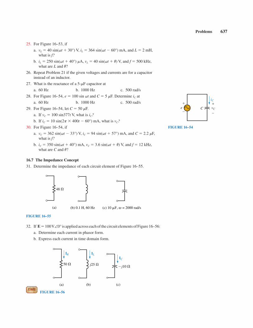
25. For Figure 16–53, if
a. vL 40 sin(qt 30°) V, iL 364 sin(qt 60°) mA, and L 2 mH,what is f?
b. iL 250 sin(qt 40°) mA, vL 40 sin(qt v) V, and f 500 kHz,what are L and v?
26. Repeat Problem 21 if the given voltages and currents are for a capacitorinstead of an inductor.
27. What is the reactance of a 5-mF capacitor at
a. 60 Hz b. 1000 Hz c. 500 rad/s
28. For Figure 16–54, e 100 sin qt and C 5 mF. Determine iC at
a. 60 Hz b. 1000 Hz c. 500 rad/s
29. For Figure 16–54, let C 50 mF.
a. If vC 100 sin377t V, what is iC?
b. If iC 10 sin(2p 400t 60°) mA, what is vC?
30. For Figure 16–54, if
a. vC 362 sin(qt 33°) V, iC 94 sin(qt 57°) mA, and C 2.2 mF,what is f?
b. iC 350 sin(qt 40°) mA, vC 3.6 sin(qt v) V, and f 12 kHz,what are C and v?
16.7 The Impedance Concept
31. Determine the impedance of each circuit element of Figure 16–55.
Problems 637
e
iC
C vC
+
−
FIGURE 16–54
48
(a) (b) 0.1 H, 60 Hz (c) 10 F, ω = 2000 rad/s
FIGURE 16–55
32. If E 100V∠0° is applied across each of the circuit elements of Figure 16–56:
a. Determine each current in phasor form.
b. Express each current in time domain form.
FIGURE 16–56
50
IR
(a)
j25
IL
(b)
j10
IC
(c)EWB

33. If the current through each circuit element of Figure 16–56 is 0.5 A∠0°:
a. Determine each voltage in phasor form.
b. Express each voltage in time domain form.
34. For each of the following, determine the impedance of the circuit elementand state whether it is resistive, inductive, or capacitive.
a. V 240 V∠30°, I 4 A∠30°.
b. V 40 V∠30°, I 4 A∠60°.
c. V 60 V∠30°, I 4 A∠60°.
d. V 140 V∠30°, I 14 mA∠120°.
35. For each circuit of Figure 16–57, determine the unknown.
36. a. If VL 120 V ∠67°, L 600 mH, and f 10 kHz, what is IL?
b. If IL 48 mA ∠43°, L 550 mH, and f 700 Hz, what is VL?
c. If VC 50 V ∠36°, C 390 pF, and f 470 kHz, what is IC?
d. If IC 95 mA ∠87°, C 6.5 nF, and f 1.2 MHz, what is VC?
16.8 Computer Analysis of AC Circuits
The version of Electronics Workbench current at the time of writing of this bookis unable to measure phase angles. Thus, in the problems that follow, we askonly for magnitudes of voltages and currents.
37. EWB Create the circuit of Figure 16–58 on the screen. (Use the ac sourcefrom the Sources Parts bin and the ammeter from the Indicators Parts bin.)Double click the ammeter symbol and set Mode to AC. Click the ON/OFFswitch at the top right hand corner of the screen to energize the circuit.Compare the measured reading against the theoretical value.
638 Chapter 16 R, L, and C Elements and the Impedance Concept
E
IL = 2 A∠90°
100 V∠0°
(a) L = 0.2 H.Determine f.
IC = 0.4 A∠90°
100 V∠0°
(b) f = 100 Hz.Determine C.
FIGURE 16–57
FIGURE 16–58
38. EWB Replace the capacitor of Figure 16–58 with a 200-mH inductor andrepeat Problem 37.
39. PSpice Create the circuit of Figure 16–53 on the screen. Use a source of100 V∠0°, L 0.2 H, and f 50 Hz. Solve for current IL (magnitude andangle). See note below.

40. PSpice Plot the reactance of a 2.39-H inductor versus frequency from1 Hz to 500 Hz and compare to Figure 16–28. Change the x-axis scale tolinear.
41. PSpice For the circuit of Problem 39, plot current magnitude versus fre-quency from f 1 Hz to f 20 Hz. Measure the current at 10 Hz and verifywith your calculator.
Note: PSpice does not permit source/inductor loops. To get around this, add avery small resistor in series, for example, R 0.00001 .
Answers to In-Process Learning Checks 639
ANSWERS TO IN-PROCESSLEARNING CHECKS
In-Process Learning Check 1
1. a. 6∠90° d. 7.21∠56.3° g. 3.61∠123.7°
b. 4∠90° e. 9.43∠122.0°
c. 4.24∠45° f. 2.24∠63.4°
2. a. j4 d. 3.83 j3.21 g. 1.64 j0.599
b. 3 j0 e. 3 j5.20
c. j2 f. 2.35 j0.855
3. 12∠40°
4. 88 j7; 16 j15
5. 288∠100°; 2∠150°
6. a. 14.70 j2.17 b. 8.94 j7.28
7. 18.0 sin(qt 56.3°)
In-Process Learning Check 2
1. 50 sin(qt 30°) A
2. 50 sin(qt 60°) A
3. 50 sin(qt 120°) A
4. 0.637 H
5. 3.98 mF
6. a. Voltage and current are in phase. Therefore, R
b. Current leads by 90°. Therefore, C
c. Current leads by 90°. Therefore, C
d. Current lags by 90°. Therefore, L
OBJECTIVES
After studying this chapter, you will beable to
• explain what is meant by active, reac-tive, and apparent power,
• compute the active power to a load,
• compute the reactive power to a load,
• compute the apparent power to a load,
• construct and use the power triangle toanalyze power to complex loads,
• compute power factor,
• explain why equipment is rated in VAinstead of watts,
• measure power in single-phase circuits,
• describe why effective resistance differsfrom geometric resistance,
• describe energy relations in ac circuits,
• use PSpice to study instantaneouspower.
KEY TERMS
Active Power
Apparent Power
Average Power
Effective Resistance
Fp
Instantaneous Power
Power Factor Correction
Power Factor
Power Triangle
Q
Reactive Power
S
Skin Effect
VA
VAR
Wattless Power
Wattmeter
OUTLINE
Introduction
Power to a Resistive Load
Power to an Inductive Load
Power to a Capacitive Load
Power in More Complex Circuits
Apparent Power
The Relationship Between P, Q, and S
Power Factor
AC Power Measurement
Effective Resistance
Energy Relationships for AC
Circuit Analysis Using Computers
Power in AC Circuits17

In Chapter 4, you studied power in dc circuits. In this chapter, we turn ourattention to power in ac circuits. In ac circuits, there are additional considera-
tions that are not present with dc. In dc circuits, for example, the only powerrelationship you encounter is P VI watts. This is referred to as real power oractive power and is the power that does useful work such as light a lamp, powera heater, run an electric motor, and so on.
In ac circuits, you also encounter this type of power. For ac circuits thatcontain reactive elements however, (i.e., inductance or capacitance), a secondcomponent of power also exists. This component, termed reactive power, repre-sents energy that oscillates back and forth throughout the system. For example,during the buildup of current in an inductance, energy flows from the powersource to the inductance to create its magnetic field. When the magnetic fieldcollapses, this energy is returned to the circuit. This movement of energy in andout of the inductance constitutes a flow of power. However, since it flows first inone direction, then in the other, it contributes nothing to the average flow ofpower from the source to the load. For this reason, reactive power is sometimesreferred to as wattless power. (A similar situation exists regarding power flow toand from the electric field of a capacitor.)
For a circuit that contains resistive as well as reactive elements, someenergy is dissipated while the remainder is shuttled back and forth as describedabove; thus, both active and reactive components of power are present. Thiscombination of real and reactive power is termed apparent power.
In this chapter, we look at all three components of power. New ideas thatemerge include the concept of power factor, the power triangle, the measurementof power in ac circuits, and the concept of effective resistance.
641
CHAPTER PREVIEW
PUTTING IT INPERSPECTIVE
Henry Cavendish
CAVENDISH, AN ENGLISH CHEMIST and physicist born in 1731, is included herenot for what he did for the emerging electrical field, but for what he didn’t do. Abrilliant man, Cavendish was 50 years ahead of his time, and his experiments inelectricity preceded and anticipated almost all the major discoveries that cameabout over the next half century (e.g., he discovered Coulomb’s law beforeCoulomb did). However, Cavendish was interested in research and knowledgepurely for its own sake and never bothered to publish most of what he learned, ineffect depriving the world of his findings and holding back the development ofthe field of electricity by many years. Cavendish’s work lay unknown for nearlya century before another great scientist, James Clerk Maxwell, had it published.Nowadays, Cavendish is better known for his work in the gravitational field thanfor his work in the electrical field. One of the amazing things he did was todetermine the mass of the earth using the rather primitive technology of his day.
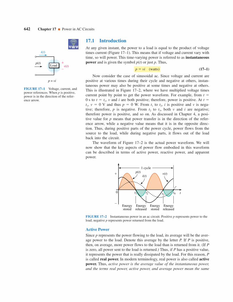
642 Chapter 17 Power in AC Circuits
FIGURE 17–1 Voltage, current, andpower references. When p is positive,power is in the direction of the refer-ence arrow.
i(t)
p(t)v(t)
Load
p = vi
0 t1 t2 t3t4
1 cyclep(t)
i(t)v(t)
Energystored
Energystored
Energyreleased
Energyreleased
t
FIGURE 17–2 Instantaneous power in an ac circuit. Positive p represents power to theload; negative p represents power returned from the load.
Active PowerSince p represents the power flowing to the load, its average will be the aver-age power to the load. Denote this average by the letter P. If P is positive,then, on average, more power flows to the load than is returned from it. (If Pis zero, all power sent to the load is returned.) Thus, if P has a positive value,it represents the power that is really dissipated by the load. For this reason, Pis called real power. In modern terminology, real power is also called activepower. Thus, active power is the average value of the instantaneous power,and the terms real power, active power, and average power mean the same
17.1 IntroductionAt any given instant, the power to a load is equal to the product of voltagetimes current (Figure 17–1). This means that if voltage and current vary withtime, so will power. This time-varying power is referred to as instantaneouspower and is given the symbol p(t) or just p. Thus,
p vi (watts) (17–1)
Now consider the case of sinusoidal ac. Since voltage and current arepositive at various times during their cycle and negative at others, instan-taneous power may also be positive at some times and negative at others.This is illustrated in Figure 17–2, where we have multiplied voltage timescurrent point by point to get the power waveform. For example, from t 0 s to t t1, v and i are both positive; therefore, power is positive. At t t1, v 0 V and thus p 0 W. From t1 to t2, i is positive and v is nega-tive; therefore, p is negative. From t2 to t3, both v and i are negative;therefore power is positive, and so on. As discussed in Chapter 4, a posi-tive value for p means that power transfer is in the direction of the refer-ence arrow, while a negative value means that it is in the opposite direc-tion. Thus, during positive parts of the power cycle, power flows from thesource to the load, while during negative parts, it flows out of the loadback into the circuit.
The waveform of Figure 17–2 is the actual power waveform. We willnow show that the key aspects of power flow embodied in this waveformcan be described in terms of active power, reactive power, and apparentpower.

thing. (We usually refer to it simply as power.) In this book, we use the termsinterchangeably.
Reactive PowerConsider again Figure 17–2. During the intervals that p is negative, power isbeing returned from the load. (This can only happen if the load containsreactive elements: L or C.) The portion of power that flows into the load thenback out is called reactive power. Since it first flows one way then the other,its average value is zero; thus, reactive power contributes nothing to theaverage power to the load.
Although reactive power does no useful work, it cannot be ignored.Extra current is required to create reactive power, and this current must besupplied by the source; this also means that conductors, circuit breakers,switches, transformers, and other equipment must be made physically largerto handle the extra current. This increases the cost of a system.
At this point, it should be noted that real power and reactive power donot exist as separate entities. Rather, they are components of the powerwaveform shown in Figure 17–2. However, as you will see, we are able toconceptually separate them for purposes of analysis.
17.2 Power to a Resistive LoadFirst consider power to a purely resistive load (Figure 17–3). Here, current isin phase with voltage. Assume i Imsin qt and v Vmsin qt. Then,
p vi (Vmsin qt)(Imsin qt) VmImsin2qt
Section 17.2 Power to a Resistive Load 643
FIGURE 17–3 Power to a purely resistive load. The peak value of p is VmIm.
0
1 cycle
p(t)
i(t)v(t)
VmIm
t
(b)
(a)
vp
i
e
Heat
Load
T2
T
Averagepower
VmIm
2
R
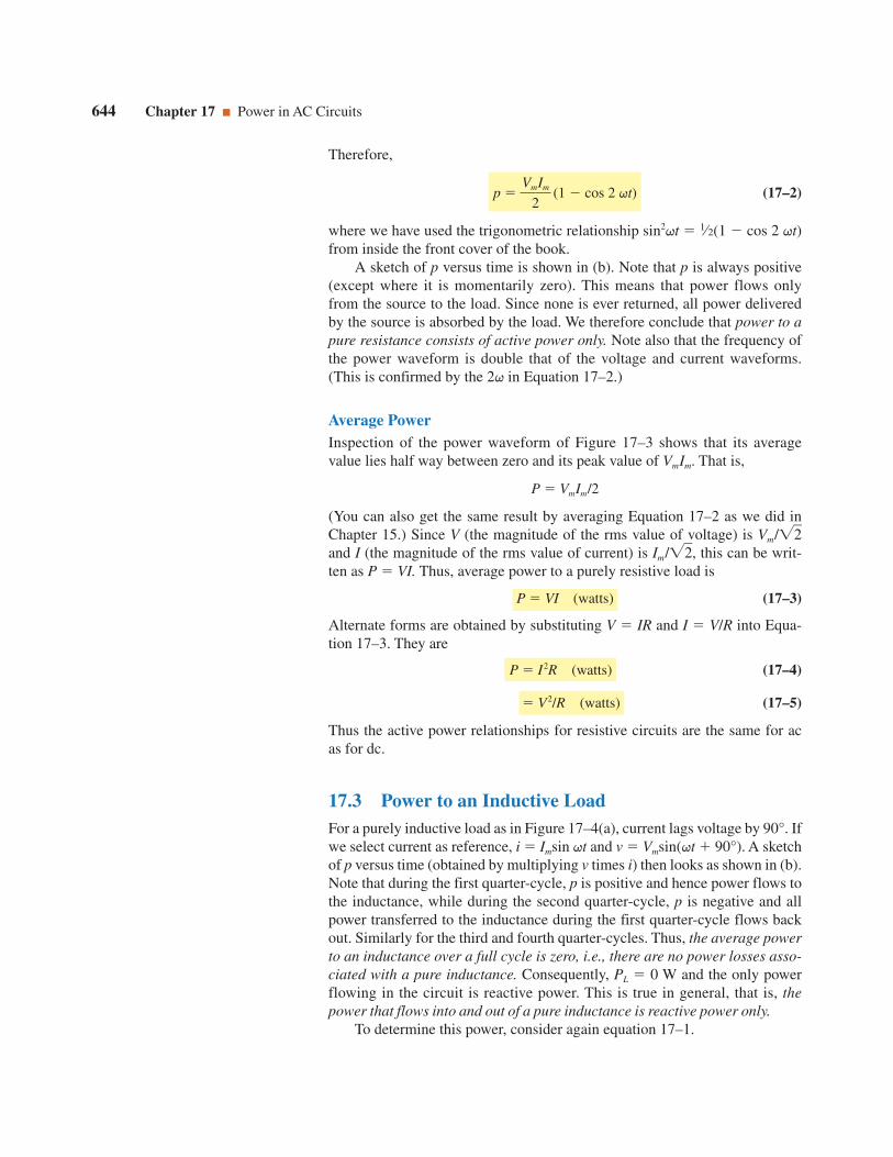
644 Chapter 17 Power in AC Circuits
Therefore,
p Vm
2
Im (1 cos 2 qt) (17–2)
where we have used the trigonometric relationship sin2qt 1⁄2(1 cos 2 qt)from inside the front cover of the book.
A sketch of p versus time is shown in (b). Note that p is always positive(except where it is momentarily zero). This means that power flows onlyfrom the source to the load. Since none is ever returned, all power deliveredby the source is absorbed by the load. We therefore conclude that power to apure resistance consists of active power only. Note also that the frequency ofthe power waveform is double that of the voltage and current waveforms.(This is confirmed by the 2q in Equation 17–2.)
Average PowerInspection of the power waveform of Figure 17–3 shows that its averagevalue lies half way between zero and its peak value of VmIm. That is,
P VmIm/2
(You can also get the same result by averaging Equation 17–2 as we did inChapter 15.) Since V (the magnitude of the rms value of voltage) is Vm/2and I (the magnitude of the rms value of current) is Im/2, this can be writ-ten as P VI. Thus, average power to a purely resistive load is
P VI (watts) (17–3)
Alternate forms are obtained by substituting V IR and I V/R into Equa-tion 17–3. They are
P I2R (watts) (17–4)
V2/R (watts) (17–5)
Thus the active power relationships for resistive circuits are the same for acas for dc.
17.3 Power to an Inductive LoadFor a purely inductive load as in Figure 17–4(a), current lags voltage by 90°. Ifwe select current as reference, i Imsin qt and v Vmsin(qt 90°). A sketchof p versus time (obtained by multiplying v times i) then looks as shown in (b).Note that during the first quarter-cycle, p is positive and hence power flows tothe inductance, while during the second quarter-cycle, p is negative and allpower transferred to the inductance during the first quarter-cycle flows backout. Similarly for the third and fourth quarter-cycles. Thus, the average powerto an inductance over a full cycle is zero, i.e., there are no power losses asso-ciated with a pure inductance. Consequently, PL 0 W and the only powerflowing in the circuit is reactive power. This is true in general, that is, thepower that flows into and out of a pure inductance is reactive power only.
To determine this power, consider again equation 17–1.

Section 17.3 Power to an Inductive Load 645
FIGURE 17–4 Power to a purely inductive load. Energy stored during each quarter-cycle is returned during the next quarter-cycle. Average power is zero.
(a) Let i = Im sin ωt
vpL
i
v = Vm sin (ωt 90°)
0
1 cyclepL(t)
i(t)v(t)VI
VI
Energystored
Energystored
Energyreleased
Energyreleased
tT4
T2
3T4
T
(b)
With v Vmsin(qt 90°) and i Imsin qt, pL vi becomes
pL VmImsin(qt 90°)sin qt
After some trigonometric manipulation, this reduces to
pL VI sin 2 qt (17–6)
where V and I are the magnitudes of the rms values of the voltage and cur-rent respectively.
The product VI in Equation 17–6 is defined as reactive power and isgiven the symbol QL. Because it represents “power” that alternately flowsinto, then out of the inductance, QL contributes nothing to the average powerto the load and, as noted earlier, is sometimes referred to as wattless power.As you will soon see, however, reactive power is of major concern in theoperation of electrical power systems.
Since QL is the product of voltage times current, its unit is the volt-amp(VA). To indicate that QL represents reactive volt-amps, an “R” is appendedto yield a new unit, the VAR (volt-amps reactive). Thus,
QL VI (VAR) (17–7)
Substituting V IXL and I V/XL yields the following alternate forms:
QL I2XL VXL
2
(VAR) (17–8)

646 Chapter 17 Power in AC Circuits
FIGURE 17–5 Power to a purely capacitive load. Average power is zero.
0
1 cycle
p(t)i(t)
v(t)VI
VI
Energyreleased
Energyreleased
Energystored
Energystored
(b)
(a) Let i = Im sin ωt
vpC
i
v = Vm sin (ωt 90°)
By convention, QL is taken to be positive. Thus, if I 4 A and XL 2 , QL (4 A)2(2 ) 32 VAR. Note that the VAR (like the watt) is ascalar quantity with magnitude only and no angle.
17.4 Power to a Capacitive LoadFor a purely capacitive load, current leads voltage by 90°. Taking current asreference, i Imsin qt and v Vmsin(qt 90°). Multiplication of v times iyields the power curve of Figure 17–5. Note that negative and positiveloops of the power wave are identical; thus, over a cycle, the power returnedto the circuit by the capacitance is exactly equal to that delivered to it bythe source. This means that the average power to a capacitance over a fullcycle is zero, i.e., there are no power losses associated with a pure capaci-tance. Consequently, PC 0 W and the only power flowing in the circuit isreactive power. This is true in general, that is, the power that flows into andout of a pure capacitance is reactive power only. This reactive power isgiven by
pC vi VmImsin qt sin(qt 90°)
which reduces to
pC VI sin 2 qt (17–9)

Section 17.4 Power to a Capacitive Load 647
EXAMPLE 17–1 For each circuit of Figure 17–6, determine real and reac-tive power.
Solution Only voltage and current magnitudes are needed.
a. I 100 V/25 4 A. P VI (100 V)(4 A) 400 W. Q 0 VAR
b. I 100 V/20 5 A. Q VI (100 V)(5 A) 500 VAR (ind.). P 0 W
c. I 100V/40 2.5A. Q VI (100V)(2.5A) 250VAR (cap.). P 0W
The answer for (c) can also be expressed as Q 250 VAR.
FIGURE 17–6
where V and I are the magnitudes of the rms values of the voltage and cur-rent respectively. Now define the product VI as QC. This product representsreactive power. That is,
QC VI (VAR) (17–10)
Since V IXC and I V/XC, QC can also be expressed as
QC I2XC XV
C
2
(VAR) (17–11)
By convention, reactive power to capacitance is defined as negative.Thus, if I 4 A and XC 2 , then I2XC (4 A)2(2 ) 32 VAR. We caneither explicitly show the minus sign as QC 32 VAR or imply it by stat-ing that Q represents capacitive vars, i.e. QC 32 VAR (cap.).
100 V∠0°
I R
(a) R 25 Ω
100 V∠0°
I XL
(b) XL 20 Ω
100 V∠0°
IXC
(c) XC 40 Ω

17.5 Power in More Complex CircuitsThe relationships described above were developed using the load of Figure17–1. However, they hold true for every element in a circuit, no matter howcomplex the circuit or how its elements are interconnected. Further, in anycircuit, total real power PT is found by summing real power to all circuitelements, while total reactive power QT is found by summing reactivepower, taking into account that inductive Q is positive and capacitive Q isnegative.
It is sometimes convenient to show power to circuit elements symboli-cally as illustrated in the next example.
648 Chapter 17 Power in AC Circuits
PRACTICEPROBLEMS 1
1. If the power at some instant in Figure 17–1 is p 27 W, in what directionis the power at that instant?
2. For a purely resistive load, v and i are in phase. Given v 10 sin qt V andi 5 sin qt A. Using graph paper, carefully plot v and i at 30° intervals. Nowmultiply the values of v and i at these points and plot the power. (The resultshould look like Figure 17–3(b).
a. From the graph, determine the peak power and average power.
b. Compute power using P VI and compare to the average value deter-mined in (a).
3. Repeat Example 17–1 using equations 17–4, 17–5, 17–8, and 17–11.
Answers:1. From the load to the source.
2. a. 50 W; 25 W
b. Same
EXAMPLE 17–2 For the RL circuit of Figure 17–7(a), I 5 A. DetermineP and Q.
SolutionP I2R (5 A)2(3 ) 75 W
Q QL I2XL (5 A)2(4 ) 100 VAR (ind.)
These can be represented symbolically as in Figure 17–7(b).
FIGURE 17–7 From the terminals, P and Q are the same for both (a) and (b).
5 A
(a)
R = 3 XL = 4
PQ
75 W 100 VAR
(b) Symbolic representation
PQ
(ind.)

In terms of determining total P and Q, it does not matter how the circuitor system is connected or what electrical elements it contains. Elements canbe connected in series, in parallel, or in series-parallel, for example, and thesystem can contain electric motors and the like, and total P is still found bysumming the power to individual elements, while total Q is found by alge-braically summing their reactive powers.
Section 17.5 Power in More Complex Circuits 649
EXAMPLE 17–3 For the RC circuit of Figure 17–8(a), determine P and Q.
SolutionP V2/R (40 V)2/(20 ) 80 W
Q QC V2/XC (40 V)2/(80 ) 20 VAR (cap.)
These can be represented symbolically as in Figure 17–8(b).
FIGURE 17–8 From the terminals, P and Q are the same for both (a) and (b).
20 80 V40 V
V
(a)
20 VAR80 WPQ
(cap.)
(b)
EXAMPLE 17–4a. For Figure 17–9(a), compute PT and QT.
b. Reduce the circuit to its simplest form.
(a)
20 A10 Ω 200 V
5 Ω
XL
R 3 Ω XC1 6 Ω
XC2
(b)
PT
QT
1200 W 2400 VAR(cap.)
4000VAR(cap.)
8000VAR(ind.)
FIGURE 17–9

Solutiona. P I2R (20 A)2(3 ) 1200 W
QC1 I2XC1
(20 A)2(6 ) 2400 VAR (cap.)
QC2
X
V
C
22
2
(2(1000
V
))2
4000 VAR (cap.)
QL V
XL
22
(20
50V)2
8000 VAR (ind.)
These are represented symbolically in part (b). PT 1200 W and QT 2400 VAR 4000 VAR 8000 VAR 1600 VAR. Thus, the load is netinductive as shown in (c).
b. QT I2Xeq. Thus, Xeq QT/I2 (1600 VAR)/(20 A)2 4 . Circuit resis-tance remains unchanged. Thus, the equivalent is as shown in (d).
17.6 Apparent PowerWhen a load has voltage V across it and current I through it as in Figure 17–11,the power that appears to flow to it is VI. However, if the load contains bothresistance and reactance, this product represents neither real power nor reactive
650 Chapter 17 Power in AC Circuits
(c)
20 A
1200 W
1600VAR(ind.)
(d)
Xeq
R
3 Ω
j 4 Ω
FIGURE 17–9 Continued.
PRACTICEPROBLEMS 2
For the circuit of Figure 17–10, PT 1.9 kW and QT 900 VAR (ind.). Deter-mine P2 and Q2.
Answer: 300 W 400 VAR (cap.)
FIGURE 17–10
1.4 kW800 VAR
P2 = ?Q2 = ?
200 W500 VAR
PTQT
(ind.)
Load 2
Load 3Load 1
(ind.)
I
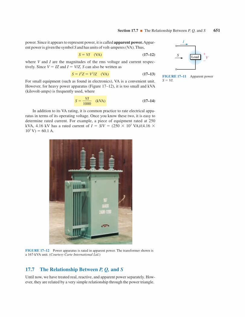
Section 17.7 The Relationship Between P, Q, and S 651
I
SV
Load
FIGURE 17–11 Apparent power S VI.
FIGURE 17–12 Power apparatus is rated in apparent power. The transformer shown isa 167-kVA unit. (Courtesy Carte International Ltd.)
17.7 The Relationship Between P, Q, and SUntil now, we have treated real, reactive, and apparent power separately. How-ever, they are related by a very simple relationship through the power triangle.
power. Since it appears to represent power, it is called apparent power. Appar-ent power is given the symbol S and has units of volt-amperes (VA). Thus,
S VI (VA) (17–12)
where V and I are the magnitudes of the rms voltage and current respec-tively. Since V IZ and I V/Z, S can also be written as
S I2Z V2/Z (VA) (17–13)
For small equipment (such as found in electronics), VA is a convenient unit.However, for heavy power apparatus (Figure 17–12), it is too small and kVA(kilovolt-amps) is frequently used, where
S 10
V0I0
(kVA) (17–14)
In addition to its VA rating, it is common practice to rate electrical appa-ratus in terms of its operating voltage. Once you know these two, it is easy todetermine rated current. For example, a piece of equipment rated at 250kVA, 4.16 kV has a rated current of I S/V (250 103 VA)/(4.16 103 V) 60.1 A.
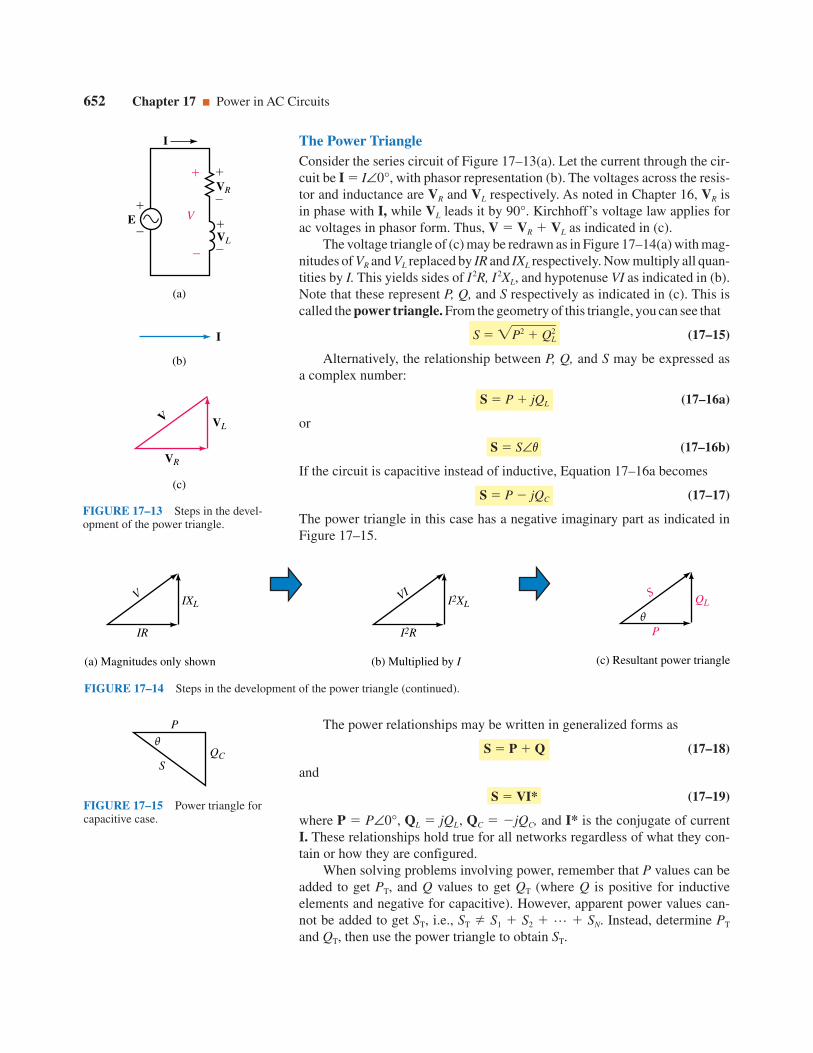
652 Chapter 17 Power in AC Circuits
E
VR
VLV
(c)
(b)
(a)
I
I
V
VR
VL
FIGURE 17–13 Steps in the devel-opment of the power triangle.
FIGURE 17–14 Steps in the development of the power triangle (continued).
IR
IXLV
(a) Magnitudes only shown
I2R
I2XLVI
(b) Multiplied by I
P
QLS
(c) Resultant power triangle
θ
FIGURE 17–15 Power triangle forcapacitive case.
θ
S
P
QC
The Power TriangleConsider the series circuit of Figure 17–13(a). Let the current through the cir-cuit be I I∠0°, with phasor representation (b). The voltages across the resis-tor and inductance are VR and VL respectively. As noted in Chapter 16, VR isin phase with I, while VL leads it by 90°. Kirchhoff’s voltage law applies forac voltages in phasor form. Thus, V VR VL as indicated in (c).
The voltage triangle of (c) may be redrawn as in Figure 17–14(a) with mag-nitudes of VR and VL replaced by IR and IXL respectively. Now multiply all quan-tities by I. This yields sides of I2R, I2XL, and hypotenuse VI as indicated in (b).Note that these represent P, Q, and S respectively as indicated in (c). This iscalled the power triangle. From the geometry of this triangle, you can see that
S P2 Q2L (17–15)
Alternatively, the relationship between P, Q, and S may be expressed asa complex number:
S P jQL (17–16a)
or
S S∠v (17–16b)
If the circuit is capacitive instead of inductive, Equation 17–16a becomes
S P jQC (17–17)
The power triangle in this case has a negative imaginary part as indicated inFigure 17–15.
The power relationships may be written in generalized forms as
S P Q (17–18)
and
S VI* (17–19)
where P P∠0°, QL jQL, QC jQC, and I* is the conjugate of currentI. These relationships hold true for all networks regardless of what they con-tain or how they are configured.
When solving problems involving power, remember that P values can beadded to get PT, and Q values to get QT (where Q is positive for inductiveelements and negative for capacitive). However, apparent power values can-not be added to get ST, i.e., ST S1 S2 … SN. Instead, determine PT
and QT, then use the power triangle to obtain ST.

Section 17.7 The Relationship Between P, Q, and S 653
EXAMPLE 17–5 The P and Q values for a circuit are shown in Figure17–16(a).
a. Determine the power triangle.
b. Determine the magnitude of the current supplied by the source.
FIGURE 17–16
Solutiona. PT 700 800 80 120 1700 W
QT 1300 600 100 1200 600 VAR 600 VAR (cap.)
ST PT jQT 1700 j600 1803∠19.4° VA
The power triangle is as shown. The load is net capacitive.
b. I ST/E 1803 VA/120 V 15.0 A
120 V
80 W
100 VAR
120 W1200 VAR
700 W1300 VAR
(a)
(cap.)(cap.)
(ind.)
800 W600 VAR
(cap.)
I
19.4°
PT = 1700 W
ST = 1803 VA
QT = 600 VAR(cap.)
θT
(b)
EXAMPLE 17–6 A generator supplies power to an electric heater, aninductive element, and a capacitor as in Figure 17–17(a).
a. Find P and Q for each load.
b. Find total active and reactive power supplied by the generator.
c. Draw the power triangle for the combined loads and determine total appar-ent power.
d. Find the current supplied by the generator.
(a)
6 Ω 24 Ω
XC XL
2.5 kWheater
120 V∠0°
FIGURE 17–17

654 Chapter 17 Power in AC Circuits
Solutiona. The components of power are as follows:
Heater: PH 2.5 kW QH 0 VAR
Inductor: PL 0 W QL VXL
2
(12
60V)2
2.4 kVAR (ind.)
Capacitor: PC 0 W QC XV
C
2
(1
2240
V)2
600 VAR (cap.)
b. PT 2.5 kW 0 W 0 W 2.5 kW
QT 0 VAR 2.4 kVAR 600 VAR 1.8 kVAR (ind.)
c. The power triangle is sketched as Figure 17–7(b). Both the hypotenuseand the angle can be obtained easily using rectangular to polar conversion.ST PT jQT 2500 j1800 3081∠35.8°. Thus, apparent power isST 3081 VA.
d. I S
ET
3018210
VVA
25.7 A
FIGURE 17–17 Continued.
(b)
1.8 kVAR
S T 3081 V
A
35.8°
QT
PT 2.5 kW
Active and Reactive Power EquationsAn examination of the power triangle of Figures 17–14 and 17–15 showsthat P and Q may be expressed respectively as
P VI cos v S cos v (W) (17–20)
and
Q VI sin v S sin v (VAR) (17–21)
where V and I are the magnitudes of the rms values of the voltage and cur-rent respectively and v is the angle between them. P is always positive, whileQ is positive for inductive circuits and negative for capacitive circuits. Thus,if V 120 volts, I 50 A, and v 30°, P (120)(50)cos 30° 5196 Wand Q (120)(50)sin 30° 3000 VAR.
17.8 Power FactorThe quantity cos v in Equation 17–20 is defined as power factor and isgiven the symbol Fp. Thus,
Fp cos v (17–22)
From Equation 17–20, we see that Fp may be computed as the ratio of realpower to apparent power. Thus,
cos v P/S (17–23)
Power factor is expressed as a number or as a percent. From Equation 17–23,it is apparent that power factor cannot exceed 1.0 (or 100% if expressed inpercent).
The power factor angle v is of interest. It can be found as
v cos1(P/S) (17–24)
Angle v is the angle between voltage and current. For a pure resistance,therefore, v 0°. For a pure inductance, v 90°; for a pure capacitance,v 90°. For a circuit containing both resistance and inductance, v will besomewhere between 0° and 90°; for a circuit containing both resistance andcapacitance, v will be somewhere between 0° and 90°.
Unity, Lagging, and Leading Power FactorAs indicated by Equation 17–23, a load’s power factor shows how much ofits apparent power is actually real power. For example, for a purely resistivecircuit, v 0° and Fp cos 0° 1.0. Therefore, P VI (watts) and all theload’s apparent power is real power. This case (Fp 1) is referred to as unitypower factor.
For a load containing only resistance and inductance, the load currentlags voltage. The power factor in this case is described as lagging. On theother hand, for a load containing only resistance and capacitance, currentleads voltage and the power factor is described as leading. Thus, an induc-tive circuit has a lagging power factor, while a capacitive circuit has a lead-ing power factor.
A load with a very poor power factor can draw excessive current. This isdiscussed next.
Section 17.8 Power Factor 655
PRACTICEPROBLEMS 3
A 208-V generator supplies power to a group of three loads. Load 1 has anapparent power of 500 VA with v 36.87° (i.e., it is net inductive). Load 2 hasan apparent power of 1000 VA and is net capacitive with a power triangle angleof 53.13°. Load 3 is purely resistive with power P3 200 W. Determine thepower triangle for the combined loads and the generator current.
Answers: ST 1300 VA, vT 22.6°, I 6.25 A
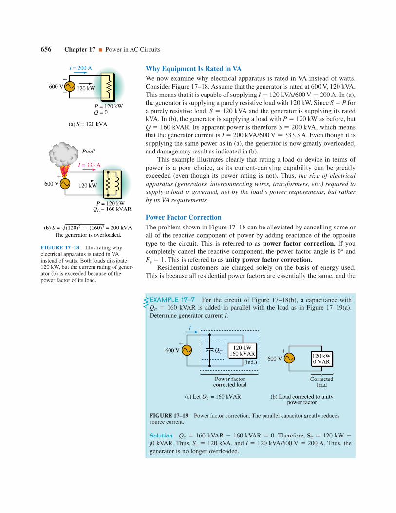
Why Equipment Is Rated in VAWe now examine why electrical apparatus is rated in VA instead of watts.Consider Figure 17–18. Assume that the generator is rated at 600 V, 120 kVA.This means that it is capable of supplying I 120 kVA/600 V 200 A. In (a),the generator is supplying a purely resistive load with 120 kW. Since S P fora purely resistive load, S 120 kVA and the generator is supplying its ratedkVA. In (b), the generator is supplying a load with P 120 kW as before, butQ 160 kVAR. Its apparent power is therefore S 200 kVA, which meansthat the generator current is I 200 kVA/600 V 333.3 A. Even though it issupplying the same power as in (a), the generator is now greatly overloaded,and damage may result as indicated in (b).
This example illustrates clearly that rating a load or device in terms ofpower is a poor choice, as its current-carrying capability can be greatlyexceeded (even though its power rating is not). Thus, the size of electricalapparatus (generators, interconnecting wires, transformers, etc.) required tosupply a load is governed, not by the load’s power requirements, but ratherby its VA requirements.
Power Factor CorrectionThe problem shown in Figure 17–18 can be alleviated by cancelling some orall of the reactive component of power by adding reactance of the oppositetype to the circuit. This is referred to as power factor correction. If youcompletely cancel the reactive component, the power factor angle is 0° andFp 1. This is referred to as unity power factor correction.
Residential customers are charged solely on the basis of energy used.This is because all residential power factors are essentially the same, and the
656 Chapter 17 Power in AC Circuits
FIGURE 17–18 Illustrating whyelectrical apparatus is rated in VAinstead of watts. Both loads dissipate120 kW, but the current rating of gener-ator (b) is exceeded because of thepower factor of its load.
600 V
Poof!
I = 333 A
120 kW
P = 120 kW
600 V
I = 200 A
120 kW
P = 120 kW
(b) S = (120)2 (160)2 = 200 kVAThe generator is overloaded.
(a) S = 120 kVA
Q = 0
QL = 160 kVAR
EXAMPLE 17–7 For the circuit of Figure 17–18(b), a capacitance withQC 160 kVAR is added in parallel with the load as in Figure 17–19(a).Determine generator current I.
Solution QT 160 kVAR 160 kVAR 0. Therefore, ST 120 kW j0 kVAR. Thus, ST 120 kVA, and I 120 kVA/600 V 200 A. Thus, thegenerator is no longer overloaded.
FIGURE 17–19 Power factor correction. The parallel capacitor greatly reducessource current.
600 V QC
(ind.)
120 kW160 kVAR
Power factorcorrected load
I
(a) Let QC = 160 kVAR
600 V
120 kW0 VAR
Correctedload
(b) Load corrected to unitypower factor

power factor effect is simply built into the tariff. Industrial customers, on theother hand, have widely different power factors, and the electrical utilitymay have to take the power factors of these customers into account.
To illustrate, assume that the loads of Figures 17–18(a) and (b) are twosmall industrial plants. If the utility based its charge solely on power, bothcustomers would pay the same amount. However, it costs the utility more tosupply customer (b) since larger conductors, larger transformers, largerswitchgear, and so on are required to handle the larger current. For this rea-son, industrial customers may pay a penalty if their power factor dropsbelow a prescribed value.
Section 17.8 Power Factor 657
EXAMPLE 17–8 An industrial client is charged a penalty if the plant powerfactor drops below 0.85. The equivalent plant loads are as shown in Figure17–20. The frequency is 60 Hz.
a. Determine PT and QT.
b. Determine what value of capacitance (in microfarads) is required to bringthe power factor up to 0.85.
c. Determine generator current before and after correction.
Solutiona. The components of power are as follows:
Lights: P 12 kW, Q 0 kVAR
Furnace: P I2R (150)2(2.4) 54 kW
Q I2X (150)2(3.2) 72 kVAR (ind.)
Motor: vm cos1(0.8) 36.9°. Thus, from the motor power triangle,
Qm Pm tan vm 80 tan 36.9° 60 kVAR (ind.)
Total: PT 12 kW 54 kW 80 kW 146 kW
QT 0 72 kVAR 60 kVAR 132 kVAR
(a)
600 V
150 A
Lights12 kW
Electric Furnace2.4 j3.2
Motor loads80 kW
0.8 Fp (lag)
Plant loads
EWB FIGURE 17–20
θm
Pm = 80 kW
Qm
b) Power triangle for motor.

658 Chapter 17 Power in AC Circuits
b. The power triangle for the plant is shown in Figure 17–21(a). However, wemust correct the power factor to 0.85. Thus we need v cos1(0.85) 31.8°, where v is the power factor angle of the corrected load as indicatedin Figure 17–21(b). The maximum reactive power that we can tolerate isthus Q
T PT tan v 146 tan 31.8° 90.5 kVAR.
Now consider Figure 17–22. QT QC 132 kVAR, where Q
T 90.5 kVAR. Therefore, QC 41.5 kVAR 41.5 kVAR (cap.). But QC V 2/XC. Therefore, XC V 2/QC (600)2/41.5 kVAR 8.67 . But XC 1/qC. Thus a capacitor of
C q
1XC
(2p)(60
1)(8.67) 306 F
will provide the required correction.
FIGURE 17–21 Initial and final power triangles. Note that PT does not changewhen we correct the power factor.
FIGURE 17–22
c. For the original circuit Figure 17–21(a), ST 196.8 kVA. Thus,
I S
ET
19660.80
kVVA
328 A
For the corrected circuit 17–21(b), ST 171.8 kVA and
I 17
610.80
kVVA
286 A
Thus, power factor correction has dropped the current by 42 A.
(a) Power triangle forthe plant
42.1°PT = 146 kW
QT = 132 kVAR19
6.8 kV
A
θ' = 31.8°PT = 146 kW
171.8 Q'T
(b) Power triangle after correction
= PT tan θ'= 90.5 kVAR
600 V QC
(ind.)
146 kW132 kVAR
Plant
Corrected load
PT
Q'T

In practice, almost all loads (industrial, residential, and commercial) areinductive due to the presence of motors, fluorescent lamp ballasts, and thelike. Consequently, you will likely never run into capacitive loads that needpower factor correcting.
Section 17.9 AC Power Measurement 659
PRACTICEPROBLEMS 4
1. Repeat Example 17–8 except correct the power factor to unity.
2. Due to plant expansion, 102 kW of purely resistive load is added to the plantof Figure 17–20. Determine whether power factor correction is needed to cor-rect the expanded plant to 0.85 Fp, or better.
Answers:1. 973 mF, 243 A. Other answers remain unchanged.
2. Fp 0.88. No correction needed.
IN-PROCESSLEARNINGCHECK 1
1. Sketch the power triangle for Figure 17–9(c). Using this triangle, determinethe magnitude of the applied voltage.
2. For Figure 17–10, assume a source of E 240 volts, P2 300 W, and Q2 400 VAR (cap.). What is the magnitude of the source current I?
3. What is the power factor of each of the circuits of Figure 17–7, 17–8, and17–9? Indicate whether they are leading or lagging.
4. Consider the circuit of Figure 17–18(b). If P 100 kW and QL 80 kVAR,is the source overloaded, assuming it is capable of handling a 120-kVA load?
(Answers are at the end of the chapter.)
17.9 AC Power MeasurementTo measure power in an ac circuit, you need a wattmeter (since the productof voltage times current is not sufficient to determine ac power). Figure17–23 shows such a meter. It is a digital device that monitors voltage andcurrent and from these, computes and displays power. (You may alsoencounter older electrodynamometer type wattmeters, i.e., electromechanicalanalog instruments that use a pivoted pointer to indicate the power readingon a scale, much like the analog meters of Chapter 2. Although their detailsdiffer dramatically from the electronic types, the manner in which they areconnected in a circuit to measure power is the same. Thus, the measurementtechniques described below apply to them as well.)
To help understand power measurement, consider Figure 17–1. Instan-taneous load power is the product of load voltage times load current, andaverage power is the average of this product. One way to implement powermeasurement is therefore to create a meter with a current sensing circuit, avoltage sensing circuit, a multiplier circuit, and an averaging circuit. Figure17–24 shows a simplified symbolic representation of such an instrument.Current is passed through its current coil (CC) to create a magnetic fieldproportional to the current, and a sensor circuit connected across the loadvoltage reacts with this field to produce an output voltage proportional tothe product of instantaneous voltage and current (i.e., proportional to

660 Chapter 17 Power in AC Circuits
FIGURE 17–23 Multifunction power/energy meter. It can measure active power (W), reactive power (VARs),apparent power (VA), power factor, energy, and more.
FIGURE 17–24 Conceptual representation of a wattmeter.
CC
CC Current coil
Load current
Voltagesensingcircuit
Vload
instantaneous power). An averaging circuit averages this voltage and drivesa display to indicate average power. (The scheme used by the meter of Fig-ure 17–23 is actually considerably more sophisticated than this because itmeasures many things besides power—e.g., it measures, VARs, VA, energy,etc. However, the basic idea is conceptually correct.)
Figure 17–25 shows how to connect a wattmeter (whether electronic orelectromechanical) into a circuit. Load current passes through its current coilcircuit, and load voltage is impressed across its voltage sensing circuit. Withthis connection, the wattmeter computes and displays the product of themagnitude of the load voltage, the magnitude of the load current, and thecosine of the angle between them, i.e. Vload Iload cos vload. Thus, it measuresload power. Note the marking on the terminals. You usually connect themeter so that load current enters the current terminal and the higher poten-tial end of the load is connected to the voltage terminal. On many meters,the voltage terminal is internally connected so that only three terminalsare brought out as in Figure 17–26.
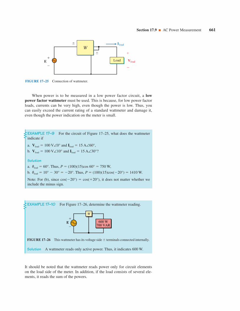
When power is to be measured in a low power factor circuit, a lowpower factor wattmeter must be used. This is because, for low power factorloads, currents can be very high, even though the power is low. Thus, youcan easily exceed the current rating of a standard wattmeter and damage it,even though the power indication on the meter is small.
Section 17.9 AC Power Measurement 661
Vload
I load
E
Load
W
FIGURE 17–25 Connection of wattmeter.
EXAMPLE 17–9 For the circuit of Figure 17–25, what does the wattmeterindicate if
a. Vload 100 V∠0° and Iload 15 A∠60°,
b. Vload 100 V∠10° and Iload 15 A∠30°?
Solutiona. vload 60°. Thus, P (100)(15)cos 60° 750 W,
b. vload 10° 30° 20°. Thus, P (100)(15)cos(20°) 1410 W.
Note: For (b), since cos(20°) cos(20°), it does not matter whether weinclude the minus sign.
EXAMPLE 17–10 For Figure 17–26, determine the wattmeter reading.
Solution A wattmeter reads only active power. Thus, it indicates 600 W.
E
600 W700 VAR
W
FIGURE 17–26 This wattmeter has its voltage side terminals connected internally.
It should be noted that the wattmeter reads power only for circuit elementson the load side of the meter. In addition, if the load consists of several ele-ments, it reads the sum of the powers.
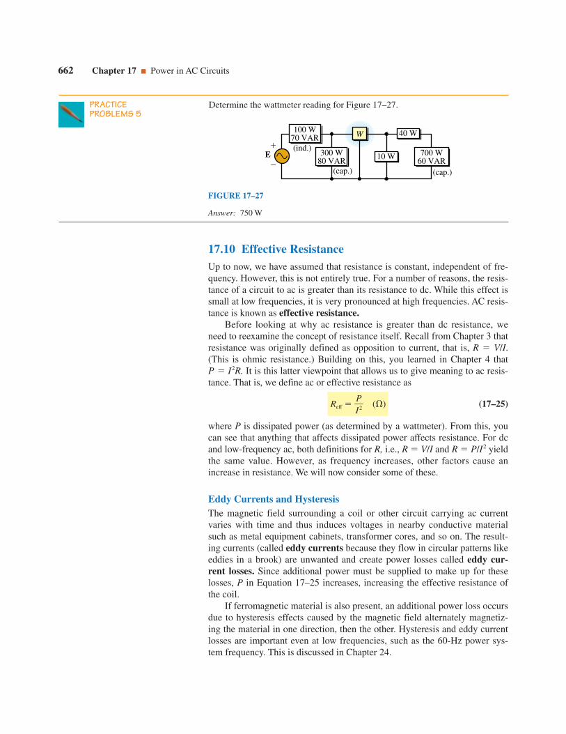
17.10 Effective ResistanceUp to now, we have assumed that resistance is constant, independent of fre-quency. However, this is not entirely true. For a number of reasons, the resis-tance of a circuit to ac is greater than its resistance to dc. While this effect issmall at low frequencies, it is very pronounced at high frequencies. AC resis-tance is known as effective resistance.
Before looking at why ac resistance is greater than dc resistance, weneed to reexamine the concept of resistance itself. Recall from Chapter 3 thatresistance was originally defined as opposition to current, that is, R V/I.(This is ohmic resistance.) Building on this, you learned in Chapter 4 thatP I2R. It is this latter viewpoint that allows us to give meaning to ac resis-tance. That is, we define ac or effective resistance as
Reff IP
2 () (17–25)
where P is dissipated power (as determined by a wattmeter). From this, youcan see that anything that affects dissipated power affects resistance. For dcand low-frequency ac, both definitions for R, i.e., R V/I and R P/I2 yieldthe same value. However, as frequency increases, other factors cause anincrease in resistance. We will now consider some of these.
Eddy Currents and HysteresisThe magnetic field surrounding a coil or other circuit carrying ac currentvaries with time and thus induces voltages in nearby conductive materialsuch as metal equipment cabinets, transformer cores, and so on. The result-ing currents (called eddy currents because they flow in circular patterns likeeddies in a brook) are unwanted and create power losses called eddy cur-rent losses. Since additional power must be supplied to make up for theselosses, P in Equation 17–25 increases, increasing the effective resistance ofthe coil.
If ferromagnetic material is also present, an additional power loss occursdue to hysteresis effects caused by the magnetic field alternately magnetiz-ing the material in one direction, then the other. Hysteresis and eddy currentlosses are important even at low frequencies, such as the 60-Hz power sys-tem frequency. This is discussed in Chapter 24.
662 Chapter 17 Power in AC Circuits
PRACTICEPROBLEMS 5
Determine the wattmeter reading for Figure 17–27.
Answer: 750 W
E
700 W60 VAR
100 W70 VAR W
10 W
40 W
(ind.)
(cap.)(cap.)
300 W80 VAR
FIGURE 17–27

Radiation ResistanceAt high frequencies some of the energy supplied to a circuit escapes as radi-ated energy. For example, a radio transmitter supplies power to an antenna,where it is converted into radio waves and radiated into space. The resistanceeffect here is known as radiation resistance. This resistance is much higherthan simple dc resistance. For example, a TV transmitting antenna may havea resistance of a fraction of an ohm to dc but several hundred ohms effectiveresistance at its operating frequency.
17.11 Energy Relationships for ACRecall, power and energy are related by the equation p dw/dt. Thus,energy can be found by integration as
W pdt vidt (17–26)
InductanceFor an inductance, v Ldi/dt. Substituting this into Equation 17–26, can-celling dt, and rearranging terms yields
WL Ldditidt Lidi (17–27)
Skin EffectMagnetically induced voltages created inside a conductor by its own chang-ing magnetic field force electrons to the periphery of the conductor (Figure17–28), resulting in a nonuniform distribution of current, with current den-sity greatest near the periphery and smallest in the center. This phenomenonis known as skin effect. Because the center of the wire carries little current,its cross-sectional area has effectively been reduced, thus increasing resis-tance. While skin effect is generally negligible at power line frequencies(except for conductors larger than several hundred thousand circular mils), itis so pronounced at microwave frequencies that the center of a wire carriesalmost no current. For this reason, hollow conductors are often used insteadof solid wires, as shown in Figure 17–28(c).
Section 17.11 Energy Relationships for AC 663
(a) Varying magnetic fieldcreates forces on electrons
within the conductor
i
Wire
FIGURE 17–28 Skin effect in ac circuits.
(b) This force pushes electronsoutward, leaving few freeelectrons in the center of
the conductor
Current densityvaries across
the wire.
(c) At high frequencies, theeffect is so pronouncedthat hollow conductors
may be used
1. The resistance measured by anohmmeter is dc resistance.
2. Many of the effects noted abovewill be treated in detail in yourvarious electronics courses. Wewill not pursue them furtherhere.
FINAL NOTES...

664 Chapter 17 Power in AC Circuits
FIGURE 17–29 Using PSpice to investigate instantaneous power in an ac circuit.
1. As of this writing, Electron-ics Workbench has no simpleway to plot current andpower; thus, no example isincluded here. If this changeswhen EWB is updated, wewill add examples and prob-lems to our web site.
2. If you want to include theidentification VSIN, 1000Hz,etc. on your schematic as inFigure 17–29, do it from theProperty Editor as describedin Chapter 16.
NOTES
Recall from Figure 17–4(b), energy flows into an inductor during time inter-val 0 to T/4 and is released during time interval T/4 to T/2. The process thenrepeats itself. The energy stored (and subsequently released) can thus befound by integrating power from t 0 to t T/4. Current at t 0 is 0 andcurrent at t T/4 is Im. Using these as our limits of integration, we find
WL LIm
0idi
12
LI2m LI2 (J) (17–28)
where we have used I Im/2 to express energy in terms of effective current.
CapacitanceFor a capacitance, i Cdv/dt. Substituting this into Equation 17–26 yields
WC vCddvtdt Cv dv (17–29)
Consider Figure 17–5(b). Energy stored can be found by integrating powerfrom T/4 to T/2. The corresponding limits for voltage are 0 to Vm. Thus,
WC CVm
0v dv
12
CV2m CV2 (J) (17–30)
where we have used V Vm/2. You will use these relationships later.
17.12 Circuit Analysis Using ComputersThe time-varying relationships between voltage, current and power describedearlier in this chapter can be investigated easily using PSpice. To illustrate,consider the circuit of Figure 17–3 with v 1.2 sin qt, R 0.8 and f 1000Hz. Create the circuit on the screen, including voltage and current markers asin Figure 17–29, then set VSIN parameters to VOFF 0V, VAMPL 1.2Vand FREQ 1000Hz as you did in Chapter 16. Click the New Simulation Pro-file, type fig17-29 for a name, choose Transient, set TSTOP to 1ms, then clickOK. Run the simulation and the voltage and current waveforms of Figure 17–30should appear. To plot power (i.e., the product of vi), click Trace, then AddTrace, and when the dialog box opens, use the asterisk to create the product
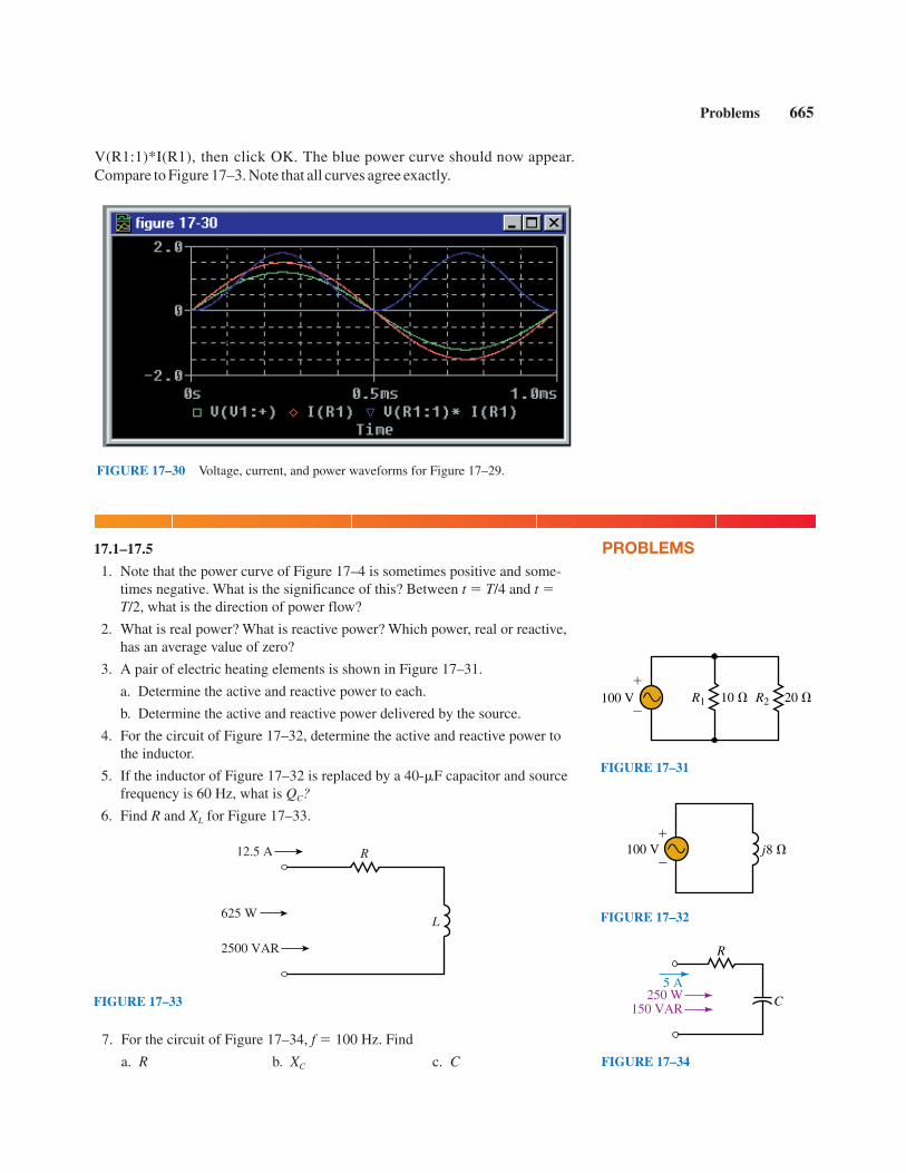
17.1–17.5
1. Note that the power curve of Figure 17–4 is sometimes positive and some-times negative. What is the significance of this? Between t T/4 and t T/2, what is the direction of power flow?
2. What is real power? What is reactive power? Which power, real or reactive,has an average value of zero?
3. A pair of electric heating elements is shown in Figure 17–31.
a. Determine the active and reactive power to each.
b. Determine the active and reactive power delivered by the source.
4. For the circuit of Figure 17–32, determine the active and reactive power tothe inductor.
5. If the inductor of Figure 17–32 is replaced by a 40-F capacitor and sourcefrequency is 60 Hz, what is QC?
6. Find R and XL for Figure 17–33.
Problems 665
FIGURE 17–30 Voltage, current, and power waveforms for Figure 17–29.
PROBLEMS
100 V
R1 10 R2 20
FIGURE 17–31
100 V
j8
FIGURE 17–32
R
L
12.5 A
625 W
2500 VAR
FIGURE 17–33
V(R1:1)*I(R1), then click OK. The blue power curve should now appear.Compare to Figure 17–3. Note that all curves agree exactly.
7. For the circuit of Figure 17–34, f 100 Hz. Find
a. R b. XC c. C
5 A250 W
150 VARC
R
FIGURE 17–34

8. For the circuit of Figure 17–35, f 10 Hz. Find
a. P b. XL c. L
9. For Figure 17–36, find XC.
666 Chapter 17 Power in AC Circuits
8 L60 VP
40 VAR
FIGURE 17–35
XC
40 Ω360 W
480 VAR
10. For Figure 17–37, XC 42.5 . Find R, P, and Q.
11. Find the total average power and the total reactive power supplied by thesource for Figure 17–38.
FIGURE 17–36
12. If the source of Figure 17–38 is reversed, what is PT and QT? What conclu-sion can you draw from this?
13. Refer to Figure 17–39. Find P2 and Q3. Is the element in Load 3 inductive orcapacitive?
FIGURE 17–37
85 VR
XC
380.1 VA
15 Ω
40 Ω10 Ω
R XL
XC4 A∠0°
FIGURE 17–38
14. For Figure 17–40, determine PT and QT.
2.9 kW
1.1 kVAR(ind.)
1200 W1400 VAR
P2600 VAR
800 WQ3
(ind.)
(cap.)
FIGURE 17–39
PT
QT
22 Ω
j6 Ω2.5 A∠0°
10 Ω
FIGURE 17–40

Problems 667
(a) (b) (c)
720 W 432 VAR(ind.)
6 ART
Leq
I = 6 A
10
j20 jXCR1
4
R3
R2720 W432 VAR (ind)
FIGURE 17–41
17.7 The Relationship Between P, Q, and S
17. For the circuit of Figure 17–7, draw the power triangle and determine theapparent power.
18. Repeat Problem 17 for Figure 17–8.
19. Ignoring the wattmeter of Figure 17–27, determine the power triangle forthe circuit as seen by the source.
20. For the circuit of Figure 17–43, what is the source current?
21. For Figure 17–44, the generator supplies 30 A. What is R?
FIGURE 17–42
600 V
2.4 A
R2
XL
40 R120
40
XC50
(cap.)
1152 W633.6 VAR
PTQT
15. For Figure 17–41, q 10 rad/s. Determine
a. RT b. R2 c. XC d. Leq
16. For Figure 17–42, determine the total PT and QT.
(ind.)
(cap.)
600 V
30 A
(ind.)6915 W
12 960 VAR
R
7450 W17 880 VAR
1377 W2750 VAR
FIGURE 17–44
(ind.)
120 V
I
(cap.)200 W0 VAR
0 W200 VAR
1200 W800 VAR
FIGURE 17–43

22. Suppose V 100 V∠60° and I 10A∠40°:
a. What is v, the angle between V and I?
b. Determine P from P VI cos v.
c. Determine Q from Q VI sin v.
d. Sketch the power triangle and from it, determine S.
e. Show that S VI* gives the same answer as (d).
23. For Figure 17–45, Sgen 4835 VA. What is R?
24. Refer to the circuit of Figure 17–16:
a. Determine the apparent power for each box.
b. Sum the apparent powers that you just computed. Why does the sum notequal ST 1803 VA as obtained in Example 17–5?
17.8 Power Factor
25. Refer to the circuit of Figure 17–46:
a. Determine PT, QT, and ST.
b. Determine whether the fuse will blow.
668 Chapter 17 Power in AC Circuits
26. A motor with an efficiency of 87% supplies 10 hp to a load (Figure 17–47).Its power factor is 0.65 (lag).
a. What is the power input to the motor?
b. What is the reactive power to the motor?
c. Draw the motor power triangle. What is the apparent power to the motor?
27. To correct the circuit power factor of Figure 17–47 to unity, a power factorcorrection capacitor is added.
a. Show where the capacitor is connected.
b. Determine its value in microfarads.
28. Consider Figure 17–20. The motor is replaced with a new unit requiringSm (120 j35) kVA. Everything else remains the same. Find the fol-lowing:
a. PT b. QT c. ST
d. Determine how much kVAR capacitive correction is needed to correct tounity Fp.
29. A small electrical utility has a 600-V, 300-kVA capacity. It supplies a fac-tory (Figure 17–48) with the power triangle shown in (b). This fully loadsthe utility. If a power factor correcting capacitor corrects the load to unity
(ind.)
600 V R
(cap.)
1014 W4608 VAR
0 W1912 VAR
FIGURE 17–45
278 W521 VAR
(ind.)
120 V
772 VAFp = 0.385
(lead)
182 VAFp = 0.8
(lag)15-Afuse
Ig
FIGURE 17–46
I
600 V60 Hz
Motor Po =η =
Fp =
10 hp0.870.65 (lag)
FIGURE 17–47
600 V
36°
Motors Lights
Otherloads
Electricutility
300 kVAcapacity
Factory loads
P
Q300 kVA
(b) Factory power triangle
(a)
FIGURE 17–48

power factor, how much more power (at unity power factor) can the utilitysell to other customers?
17.9 AC Power Measurement
30. a. Why does the wattmeter of Figure 17–49 indicate only 1200 watts?
b. Where would the wattmeter have to be placed to measure power deliv-ered by the source? Sketch the modified circuit.
c. What would the wattmeter indicate in (b)?
Problems 669
E
300 W0 VAR
700 W600 VAR
1200 W400 VAR
W
FIGURE 17–49
120 V∠50° 25 A∠20°
W
FIGURE 17–50
31. Determine the wattmeter reading for Figure 17–50.
32. Determine the wattmeter reading for Figure 17–51.
120 V
W
XC 60 Ω
40 Ω
FIGURE 17–51
17.10 Effective Resistance
33. Measurements on an iron-core solenoid coil yield the following values: V 80 V, I 400 mA, P 25.6 W, and R 140 . (The last measurementwas taken with an ohmmeter.) What is the ac resistance of the solenoidcoil?
17.12 Circuit Analysis Using Computers
34. PSpice An inductance L 1 mH has current i 4 sin (2p 1000)t. UsePSpice to investigate the power waveform and compare to Figure 17–4. Usecurrent source ISIN (see Note).
35. PSpice A 10-mF capacitor has voltage v 10 sin(qt 90°) V. UsePSpice to investigate the power waveform and compare to Figure 17–5. Usevoltage source VSIN with f 1000 Hz.
PSpice represents current intodevices. Thus, when you doubleclick a current source symbol(ISIN, IPWL, etc.) and specify acurrent waveform, you are speci-fying the current into the source.
NOTE...

670 Chapter 17 Power in AC Circuits
a. Using the principles of Chapter 10, determine the current through thecapacitor and sketch. (Also sketch the voltage waveform on your graph.)Multiply the two waveforms to obtain a plot of p(t). Compute power atits max and min points.
b. Use PSpice to verify the results. Use voltage source VPWL. You have todescribe the waveform to the source. It has a value of 0 V at t 0, 10 Vat t 1 ms, 10 V at t 3 ms, and 0 V at t 4 ms. To set these, doubleclick the source symbol and enter values via the Property Editor as fol-lows: 0 for T1, 0V for V1, 1ms for T2, 10V for V2, etc. Run the simula-tion and plot voltage, current, and power using the procedure we used tocreate Figure 17–30. Results should agree with those of (a).
37. PSpice Repeat Question 36 for a current waveform identical to Figure17–52 except that it oscillates between 2 A and 2 A applied to a 2-mHinductor. Use current source IPWL (see Note).
10 V
01 2
10 V
v
t (ms)3 4
FIGURE 17–52
In-Process Learning Check 1
1. 100 V
2. 8.76 A
3. Fig. 17–7: 0.6 (lag); Fig. 17–8: 0.97 (lead); Fig. 17–9: 0.6 (lag)
4. Yes. (S 128 kVA)
FIGURE 17–53
1600VAR
1200 W
53.13°
2000VA
ANSWERS TO IN-PROCESSLEARNING CHECKS
36. PSpice The voltage waveform of Figure 17–52 is applied to a 200-mFcapacitor.


OBJECTIVES
After studying this chapter, you will beable to
• apply Ohm’s law to analyze simpleseries circuits,
• apply the voltage divider rule to deter-mine the voltage across any element in aseries circuit,
• apply Kirchhoff’s voltage law to verifythat the summation of voltages around aclosed loop is equal to zero,
• apply Kirchhoff’s current law to verifythat the summation of currents enteringa node is equal to the summation of cur-rents leaving the same node,
• determine unknown voltage, current,and power for any series/parallel circuit,
• determine the series or parallel equiva-lent of any network consisting of a com-bination of resistors, inductors, andcapacitors.
KEY TERMS
AC Parallel Circuits
AC Series Circuits
Current Divider Rule
Frequency Effects
Impedance
Kirchhoff’s Current Law
Kirchhoff’s Voltage Law
Voltage Divider Rule
OUTLINE
Ohm’s Law for AC Circuits
AC Series Circuits
Kirchhoff’s Voltage Law and the VoltageDivider Rule
AC Parallel Circuits
Kirchhoff’s Current Law and the CurrentDivider Rule
Series-Parallel Circuits
Frequency Effects
Applications
Circuit Analysis Using Computers
AC Series-Parallel Circuits18

In this chapter we examine how simple circuits containing resistors, inductors,and capacitors behave when subjected to sinusoidal voltages and currents.
Principally, we find that the rules and laws which were developed for dc circuitswill apply equally well for ac circuits. The major difference between solving dcand ac circuits is that analysis of ac circuits requires using vector algebra.
In order to proceed successfully, it is suggested that the student spend timereviewing the important topics covered in dc analysis. These include Ohm’s law,the voltage divider rule, Kirchhoff’s voltage law, Kirchhoff’s current law, andthe current divider rule.
You will also find that a brief review of vector algebra will make yourunderstanding of this chapter more productive. In particular, you should be ableto add and subtract any number of vector quantities.
673
CHAPTER PREVIEW
PUTTING IT INPERSPECTIVE
Heinrich Rudolph Hertz
HEINRICH HERTZ WAS BORN IN HAMBURG, Germany, on February 22, 1857. Heis known mainly for his research into the transmission of electromagnetic waves.
Hertz began his career as an assistant to Hermann von Helmholtz in theBerlin Institute physics laboratory. In 1885, he was appointed Professor ofPhysics at Karlsruhe Polytechnic, where he did much to verify James ClerkMaxwell’s theories of electromagnetic waves.
In one of his experiments, Hertz discharged an induction coil with a rectan-gular loop of wire having a very small gap. When the coil discharged, a sparkjumped across the gap. He then placed a second, identical coil close to the first,but with no electrical connection. When the spark jumped across the gap of thefirst coil, a smaller spark was also induced across the second coil. Today, moreelaborate antennas use similar principles to transmit radio signals over vast dis-tances. Through further research, Hertz was able to prove that electromagneticwaves have many of the characteristics of light: they have the same speed aslight; they travel in straight lines; they can be reflected and refracted; and theycan be polarized.
Hertz’s experiments ultimately led to the development of radio communica-tion by such electrical engineers as Guglielmo Marconi and Reginald Fessenden.
Heinrich Hertz died at the age of 36 on January 1, 1894.

18.1 Ohm’s Law for AC CircuitsThis section is a brief review of the relationship between voltage and currentfor resistors, inductors, and capacitors. Unlike Chapter 16, all phasors aregiven as rms rather than as peak values. As you saw in Chapter 17, thisapproach simplifies the calculation of power.
ResistorsIn Chapter 16, we saw that when a resistor is subjected to a sinusoidal volt-age as shown in Figure 18–1, the resulting current is also sinusoidal and inphase with the voltage.
The sinusoidal voltage v Vmsin(qt v) may be written in phasor form asV V∠v. Whereas the sinusoidal expression gives the instantaneous value ofvoltage for a waveform having an amplitude of Vm (volts peak), the phasor formhas a magnitude which is the effective (or rms) value. The relationship betweenthe magnitude of the phasor and the peak of the sinusoidal voltage is given as
V Vm
2
Because the resistance vector may be expressed as ZR R∠0°, we eval-uate the current phasor as follows:
I ZV
R
RV∠∠
0v
°
VR
∠v I∠v
674 Chapter 18 AC Series-Parallel Circuits
Although currents and voltagesmay be shown in either time do-main (as sinusoidal quantities) orin phasor domain (as vectors),resistance and reactance arenever shown as sinusoidal quan-tities. The reason for this is thatwhereas currents and voltagesvary as functions of time, resis-tance and reactance do not.
NOTES...
FIGURE 18–1 Sinusoidal voltage and current for a resistor.
(a)
(b)
v R
i
v = Vm sin (ωt + θ)
2
θωt
i = Im sin (ωt + θ)
(rad)
radians

If we wish to convert the current from phasor form to its sinusoidalequivalent in the time domain, we would have i Imsin(qt v). Again, therelationship between the magnitude of the phasor and the peak value of thesinusoidal equivalent is given as
I Im
2
The voltage and current phasors may be shown on a phasor diagram asin Figure 18–2.
Because one phasor is a current and the other is a voltage, the relativelengths of these phasors are purely arbitrary. Regardless of the angle v, wesee that the voltage across and the current through a resistor will always bein phase.
Section 18.1 Ohm’s Law for AC Circuits 675
FIGURE 18–2 Voltage and currentphasors for a resistor.
j
I I ∠θ
j
V V ∠θ
θ
EXAMPLE 18–1 Refer to the resistor shown in Figure 18–3:
a. Find the sinusoidal current i using phasors.
b. Sketch the sinusoidal waveforms for v and i.
c. Sketch the phasor diagram of V and I.
Solution:a. The phasor form of the voltage is determined as follows:
v 72 sin qt ⇔ V 50.9 V∠0°
From Ohm’s law, the current phasor is determined to be
I ZV
R
5108.9
V∠∠00°°
2.83 A∠0°
which results in the sinusoidal current waveform having an amplitude of
Im (2)(2.83 A) 4.0 A
Therefore, the current i will be written as
i 4 sin qt
FIGURE 18–3
18
i
v 72 sin ωt

676 Chapter 18 AC Series-Parallel Circuits
b. The voltage and current waveforms are shown in Figure 18–4.
c. Figure 18–5 shows the voltage and current phasors.
FIGURE 18–4
FIGURE 18–5
v = 72 sin ωt
ωt
i = 4 sin ωt
3
2
j
V 50.9 V∠0
I 2.83 A∠0
EXAMPLE 18–2 Refer to the resistor of Figure 18–6:
a. Use phasor algebra to find the sinusoidal voltage, v.
b. Sketch the sinusoidal waveforms for v and i.
c. Sketch a phasor diagram showing V and I.
Solutiona. The sinusoidal current has a phasor form as follows:
i 3 103sin(qt 40°) ⇔ I 2.12 mA∠40°
FIGURE 18–6
2 k
v
i 3 × 10⁻³ sin(ωt 40)

InductorsWhen an inductor is subjected to a sinusoidal current, a sinusoidal voltage isinduced across the inductor such that the voltage across the inductor leads thecurrent waveform by exactly 90°. If we know the reactance of an inductor, thenfrom Ohm’s law the current in the inductor may be expressed in phasor form as
I ZV
L
XL
V∠∠9v
0°
XV
L
∠(v 90°)
Section 18.1 Ohm’s Law for AC Circuits 677
From Ohm’s law, the voltage across the 2-k resistor is determined as thephasor product
V IZR
(2.12 mA∠40°)(2 k∠0°)
4.24 V∠40°
The amplitude of the sinusoidal voltage is
Vm (2)(4.24 V) 6.0 V
The voltage may now be written as
v 6.0 sin(qt 40°)
b. Figure 18–7 shows the sinusoidal waveforms for v and i.
c. The corresponding phasors for the voltage and current are shown in Figure18–8.
FIGURE 18–7
FIGURE 18–8
v = 6 sin (ωt 40)
ωt40
i 3 × 10⁻³ sin(ωt 40)
j
V 4.24 V∠40
I 2.12 mA∠40
j
40

In vector form, the reactance of the inductor is given as
ZL XL∠90°
where XL qL 2pfL.
678 Chapter 18 AC Series-Parallel Circuits
EXAMPLE 18–3 Consider the inductor shown in Figure 18–9:
FIGURE 18–9
FIGURE 18–10 Sinusoidal voltage and current for an inductor.
a. Determine the sinusoidal expression for the current i using phasors.
b. Sketch the sinusoidal waveforms for v and i.
c. Sketch the phasor diagram showing V and I.
Solution:a. The phasor form of the voltage is determined as follows:
v 1.05 sin(qt 120°) ⇔ V 0.742 V∠120°
From Ohm’s law, the current phasor is determined to be
I ZV
L
0.7
2452V∠∠9102°0°
29.7 mA∠30°
The amplitude of the sinusoidal current is
Im (2)(29.7 mA) 42 mA
The current i is now written as
i 0.042 sin(qt 30°)
b. Figure 18–10 shows the sinusoidal waveforms of the voltage and current.
XL 25
i
v 1.05 sin(ωt 120)
v 1.05 sin(ωt 120°)
2
i 0.042 sin(ωt 30°)
30°
120°
ωt
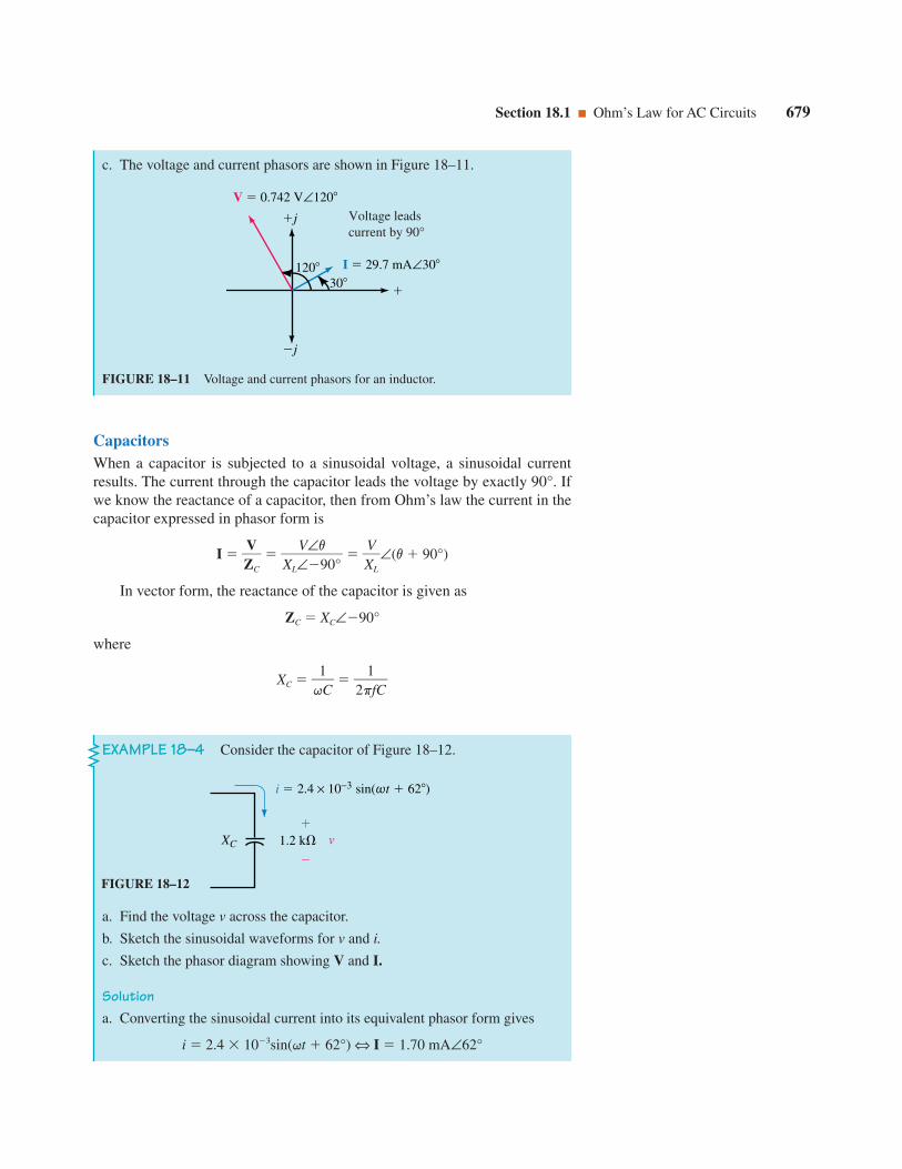
CapacitorsWhen a capacitor is subjected to a sinusoidal voltage, a sinusoidal currentresults. The current through the capacitor leads the voltage by exactly 90°. Ifwe know the reactance of a capacitor, then from Ohm’s law the current in thecapacitor expressed in phasor form is
I ZV
C
XL∠
V∠
v
90°
XV
L
∠(v 90°)
In vector form, the reactance of the capacitor is given as
ZC XC∠90°
where
XC q
1C
2p
1fC
Section 18.1 Ohm’s Law for AC Circuits 679
c. The voltage and current phasors are shown in Figure 18–11.
FIGURE 18–11 Voltage and current phasors for an inductor.
j
V 0.742 V∠120
I 29.7 mA∠30
j
30120
Voltage leadscurrent by 90°
EXAMPLE 18–4 Consider the capacitor of Figure 18–12.
FIGURE 18–12
XC
i 2.4 × 10⁻³ sin(ωt 62)
1.2 k
v
a. Find the voltage v across the capacitor.
b. Sketch the sinusoidal waveforms for v and i.
c. Sketch the phasor diagram showing V and I.
Solutiona. Converting the sinusoidal current into its equivalent phasor form gives
i 2.4 103sin(qt 62°) ⇔ I 1.70 mA∠62°

The relationships between voltage and current, as illustrated in the previ-ous three examples, will always hold for resistors, inductors, and capacitors.
680 Chapter 18 AC Series-Parallel Circuits
1. What is the phase relationship between current and voltage for a resistor?
2. What is the phase relationship between current and voltage for a capacitor?
3. What is the phase relationship between current and voltage for an inductor?
(Answers are at the end of the chapter.)
IN-PROCESSLEARNINGCHECK 1
From Ohm’s law, the phasor voltage across the capacitor must be
V IZC
(1.70 mA∠62°)(1.2 k∠90°)
2.04 V∠28°
The amplitude of the sinusoidal voltage is
Vm (2)(2.04 V) 2.88 V
The voltage v is now written as
v 2.88 sin(qt 28°)
b. Figure 18–13 shows the waveforms for v and i.
c. The corresponding phasor diagram for V and I is shown in Figure 18–14.
FIGURE 18–13 Sinusoidal voltage and current for a capacitor.
FIGURE 18–14 Voltage and current phasors for a capacitor.
v = 2.88 sin(ωt 28) i = 2.4 10−3 sin(ωt 62)
28
62
π 2π 3πωt
j
V 2.04 V∠28
I 1.70 mA∠62
j
28
62
Current leadsvoltage by 90°
18.2 AC Series CircuitsWhen we examined dc circuits we saw that the current everywhere in aseries circuit is always constant. This same applies when we have series ele-ments with an ac source. Further, we had seen that the total resistance of a dcseries circuit consisting of n resistors was determined as the summation
RT R1 R2 … Rn
When working with ac circuits we no longer work with only resistancebut also with capacitive and inductive reactance. Impedance is a term used tocollectively determine how the resistance, capacitance, and inductance“impede” the current in a circuit. The symbol for impedance is the letter Zand the unit is the ohm (). Because impedance may be made up of any com-bination of resistances and reactances, it is written as a vector quantity Z,where
Z Z∠v ()
Each impedance may be represented as a vector on the complex plane,such that the length of the vector is representative of the magnitude of theimpedance. The diagram showing one or more impedances is referred to asan impedance diagram.
Resistive impedance ZR is a vector having a magnitude of R along thepositive real axis. Inductive reactance ZL is a vector having a magnitude of
Section 18.2 AC Series Circuits 681
PRACTICEPROBLEMS 1
A voltage source, E 10 V∠30°, is applied to an inductive impedance of 50 .
a. Solve for the phasor current, I.
b. Sketch the phasor diagram for E and I.
c. Write the sinusoidal expressions for e and i.
d. Sketch the sinusoidal expressions for e and i.
Answers:a. I 0.2 A∠60°
c. e 14.1 sin(qt 30°)
i 0.283 sin(qt 60°)
PRACTICEPROBLEMS 2
A voltage source, E 10 V∠30°, is applied to a capacitive impedance of 20 .
a. Solve for the phasor current, I.
b. Sketch the phasor diagram for E and I.
c. Write the sinusoidal expressions for e and i.
d. Sketch the sinusoidal expressions for e and i.
Answers:a. I 0.5 A∠120°
c. e 14.1 sin(qt 30°)
i 0.707 sin(qt 120°)

XL along the positive imaginary axis, while the capacitive reactance ZC is avector having a magnitude of XC along the negative imaginary axis. Mathe-matically, each of the vector impedances is written as follows:
ZR R∠0° R j0 R
ZL XL∠90° 0 jXL jXL
ZC XC∠90° 0 jXC jXC
An impedance diagram showing each of the above impedances is shownin Figure 18–15.
All impedance vectors will appear in either the first or the fourth quad-rants, since the resistive impedance vector is always positive.
For a series ac circuit consisting of n impedances, as shown in Figure18–16, the total impedance of the circuit is found as the vector sum
ZT Z1 Z2 … Zn (18–1)
Consider the branch of Figure 18–17.By applying Equation 18–1, we may determine the total impedance of thecircuit as
ZT (3 j0) (0 j4 ) 3 j4
5 ∠53.13°
The above quantities are shown on an impedance diagram as in Figure18–18.
682 Chapter 18 AC Series-Parallel Circuits
FIGURE 18–15
FIGURE 18–16 FIGURE 18–17 FIGURE 18–18
j
ZC XC∠90 j XC
ZL XL∠90 j XL
j
ZR R∠0
ZT
Z1
Z2
ZnXL
3
4
R
ZT
53.13
4 ∠90
3 ∠0
ZT 3 j 4 5 ∠53.13
4
3
5
From Figure 18–18 we see that the total impedance of the series ele-ments consists of a real component and an imaginary component. The corre-sponding total impedance vector may be written in either polar or rectangu-lar form.
The rectangular form of an impedance is written as
Z R jX
If we are given the polar form of the impedance, then we may determinethe equivalent rectangular expression from
R Z cos v (18–2)
and
X Z sin v (18–3)

In the rectangular representation for impedance, the resistance term, R,is the total of all resistance looking into the network. The reactance term, X,is the difference between the total capacitive and inductive reactances. Thesign for the imaginary term will be positive if the inductive reactance isgreater than the capacitive reactance. In such a case, the impedance vectorwill appear in the first quadrant of the impedance diagram and is referred toas being an inductive impedance. If the capacitive reactance is larger, thenthe sign for the imaginary term will be negative. In such a case, the imped-ance vector will appear in the fourth quadrant of the impedance diagram andthe impedance is said to be capacitive.
The polar form of any impedance will be written in the form
Z Z∠v
The value Z is the magnitude (in ohms) of the impedance vector Z and isdetermined as follows:
Z R2 X2 () (18–4)
The corresponding angle of the impedance vector is determined as
v tan1XR
(18–5)
Whenever a capacitor and an inductor having equal reactances are placed inseries, as shown in Figure 18–19, the equivalent circuit of the two compo-nents is a short circuit since the inductive reactance will be exactly balancedby the capacitive reactance.
Any ac circuit having a total impedance with only a real component, isreferred to as a resistive circuit. In such a case, the impedance vector ZT willbe located along the positive real axis of the impedance diagram and theangle of the vector will be 0°. The condition under which series reactancesare equal is referred to as “series resonance” and is examined in greaterdetail in a later chapter.
If the impedance Z is written in polar form, then the angle v will be pos-itive for an inductive impedance and negative for a capacitive impedance. Inthe event that the circuit is purely reactive, the resulting angle v will be either90° (inductive) or 90° (capacitive). If we reexamine the impedance dia-gram of Figure 18–18, we conclude that the original circuit is inductive.
Section 18.2 AC Series Circuits 683
XC X
ZT 0
XL X
ZT jXL jXC
jX jX 0
FIGURE 18–19

684 Chapter 18 AC Series-Parallel Circuits
EXAMPLE 18–5 Consider the network of Figure 18–20.
a. Find ZT.
b. Sketch the impedance diagram for the network and indicate whether thetotal impedance of the circuit is inductive, capacitive, or resistive.
c. Use Ohm’s law to determine I, VR , and VC.
Solutiona. The total impedance is the vector sum
ZT 25 j200 (j225 )
25 j25
35.36 ∠45°
b. The corresponding impedance diagram is shown in Figure 18–21.
Because the total impedance has a negative reactance term (j25 ), ZT iscapacitive.
c. I 35.3
160
V
∠∠
0°45°
0.283 A∠45°
VR (282.8 mA∠45°)(25 ∠0°) 7.07 V∠45°
VC (282.8 mA∠45°)(225 ∠90°) 63.6 V∠45°
FIGURE 18–20
FIGURE 18–21
VC
200
I
XL
VR
225
XC
ZT10 V∠0
R 25
j
j225
ZT 25 j 25 35.36 ∠45
45
j200
j200 j225 j25

Section 18.2 AC Series Circuits 685
Notice that the magnitude of the voltage across the capacitor is manytimes larger than the source voltage applied to the circuit. This example illus-trates that the voltages across reactive elements must be calculated to ensurethat maximum ratings for the components are not exceeded.
EXAMPLE 18–6 Determine the impedance Z which must be within theindicated block of Figure 18–22 if the total impedance of the network is13 ∠22.62°.
Solution Converting the total impedance from polar to rectangular form,we get
ZT 13 ∠22.62° ⇔ 12 j5
Now, we know that the total impedance is determined from the summa-tion of the individual impedance vectors, namely
ZT 2 j10 Z 12 j5
Therefore, the impedance Z is found as
Z 12 j5 (2 j10 )
10 j5
11.18 ∠26.57°
In its most simple form, the impedance Z will consist of a series combi-nation of a 10- resistor and a capacitor having a reactance of 5 . Figure18–23 shows the elements which may be contained within Z to satisfy thegiven conditions.
FIGURE 18–22
FIGURE 18–23
ZT 13 ∠22.62
R
2
10
XL
Z
R 10
5 XC
Z 10 j 5 11.18 ∠26.57

The phase angle v for the impedance vector Z Z∠v provides the phaseangle between the voltage V across Z and the current I through the imped-ance. For an inductive impedance the voltage will lead the current by v. Ifthe impedance is capacitive, then the voltage will lag the current by anamount equal to the magnitude of v.
686 Chapter 18 AC Series-Parallel Circuits
EXAMPLE 18–7 Find the total impedance for the network of Figure 18–24.Sketch the impedance diagram showing Z1, Z2, and ZT.
Solution:ZT Z1 Z2
(50 j90 ) (30 j30 )
(80 j60 ) 100 ∠36.87°
The polar forms of the vectors Z1 and Z2 are as follows:
Z1 50 j90 102.96 ∠60.95°
Z2 30 j30 42.43 ∠45°
The resulting impedance diagram is shown in Figure 18–25.
FIGURE 18–24
FIGURE 18–25
ZT
30 j 30 Z2
50 j 90 Z1
j
ZT 100 ∠36.87
Z2 42.43 ∠45
60.95
36.87
45
Z1 102.96 ∠60.95
j

Section 18.2 AC Series Circuits 687
FIGURE 18–26
FIGURE 18–27
XL
R
ZT
I
VR
V
Z Z∠θ
R
XL
j
θ
The phase angle v is also useful for determining the average power dissi-pated by the circuit. In the simple series circuit shown in Figure 18–26, weknow that only the resistor will dissipate power.
The average power dissipated by the resistor may be determined as fol-lows:
P VRI V
R
2R I2R (18–6)
Notice that Equation 18–6 uses only the magnitudes of the voltage, cur-rent, and impedance vectors. Power is never determined by using phasorproducts.
Ohm’s law provides the magnitude of the current phasor as
I VZ
Substituting this expression into Equation 18–6, we obtain the expres-sion for power as
P VZ2
2
R VZ
2
RZ
(18–7)
From the impedance diagram of Figure 18–27, we see that
cos v RZ
The previous chapter had defined the power factor as Fp cos v, wherev is the angle between the voltage and current phasors. We now see that for aseries circuit, the power factor of the circuit can be determined from themagnitudes of resistance and total impedance.
Fp cos v RZ
(18–8)
The power factor, Fp, is said to be leading if the current leads the volt-age (capacitive circuit) and lagging if the current lags the voltage (inductivecircuit).
Now substituting the expression for the power factor into Equation18–7, we express power delivered to the circuit as
P VI cos v
Since V IZ, power may be expressed as
P VI cos v I2Z cos v VZ
2
cos v (18–9)

688 Chapter 18 AC Series-Parallel Circuits
EXAMPLE 18–8 Refer to the circuit of Figure 18–28.
a. Find the impedance ZT.
b. Calculate the power factor of the circuit.
c. Determine I.
d. Sketch the phasor diagram for E and I.
e. Find the average power delivered to the circuit by the voltage source.
f. Calculate the average power dissipated by both the resistor and the capacitor.
Solutiona. ZT 3 j4 5 ∠53.13°
b. Fp cos v 3 \5 0.6 (leading)
c. The phasor form of the applied voltage is
E (2
)(2
20 V)
∠0° 20 V∠0°
which gives a current of
I 5
2∠0
V∠53
0.°13°
4.0 A∠53.13°
d. The phasor diagram is shown in Figure 18–29.
From this phasor diagram, we see that the current phasor for the capacitivecircuit leads the voltage phasor by 53.13°.
FIGURE 18–28
FIGURE 18–29
4
I
e 202 sin ωt
3
ZT
R
XC
I 4.0 A∠53.13
j
53.13 E 20 V∠0

18.3 Kirchhoff’s Voltage Law and the Voltage Divider Rule
When a voltage is applied to impedances in series, as shown in Figure 18–30,Ohm’s law may be used to determine the voltage across any impedance as
Vx IZx
The current in the circuit is
I ZE
T
Now, by substitution we arrive at the voltage divider rule for any seriescombination of elements as
Vx ZZ
T
xE (18–10)
Section 18.3 Kirchhoff’s Voltage Law and the Voltage Divider Rule 689
PRACTICEPROBLEMS 3
A circuit consists of a voltage source E 50 V∠25° in series with L 20 mH,C 50 mF, and R 25 . The circuit operates at an angular frequency of2 krad/s.
a. Determine the current phasor, I.
b. Solve for the power factor of the circuit.
c. Calculate the average power dissipated by the circuit and verify that this isequal to the average power delivered by the source.
d. Use Ohm’s law to find VR, VL, and VC.
Answers:a. I 1.28 A∠25.19°
b. Fp 0.6402
c. P 41.0 W
d. VR 32.0 V∠25.19°
VC 12.8 V∠115.19°
VL 51.2 V∠64.81°
e. The average power delivered to the circuit by the voltage source is
P (20 V)(4 A) cos 53.13° 48.0 W
f. The average power dissipated by the resistor and capacitor will be
PR (4 A)2(3 )cos 0° 48 W
PC (4 A)2(4 )cos 90° 0 W (as expected!)
Notice that the power factor used in determining the power dissipated by eachof the elements is the power factor for that element and not the total powerfactor for the circuit.
As expected, the summation of powers dissipated by the resistor andcapacitor is equal to the total power delivered by the voltage source.

Equation 18–10 is very similar to the equation for the voltage dividerrule in dc circuits. The fundamental differences in solving ac circuits are thatwe use impedances rather than resistances and that the voltages found arephasors. Because the voltage divider rule involves solving products and quo-tients of phasors, we generally use the polar form rather than the rectangularform of phasors.
Kirchhoff’s voltage law must apply for all circuits whether they are dcor ac circuits. However, because ac circuits have voltages expressed in eithersinusoidal or phasor form, Kirchhoff’s voltage law for ac circuits may bestated as follows:
The phasor sum of voltage drops and voltage rises around a closed loop isequal to zero.
When adding phasor voltages, we find that the summation is generallydone more easily in rectangular form rather than the polar form.
690 Chapter 18 AC Series-Parallel Circuits
E
Z1
Z2
Zn
Zx
Vx
I
FIGURE 18–30
EXAMPLE 18–9 Consider the circuit of Figure 18–31.
a. Find ZT.
b. Determine the voltages VR and VL using the voltage divider rule.
c. Verify Kirchhoff’s voltage law around the closed loop.
Solutiona. ZT 5 k j12 k 13 k∠67.38°
b. VR 135k
k∠
∠67
0.°38°
(26 V∠0°) 10 V∠67.38°
VL 1312
kk
∠∠67
9.03°8°
(26 V∠0°) 24 V∠22.62°
c. Kirchhoff’s voltage law around the closed loop will give
26 V∠0° 10 V∠67.38° 24 V∠22.62° 0
(26 j0) (3.846 j9.231) (22.154 j9.231) 0
(26 3.846 22.154) j(0 9.231 9.231) 0
0 j0 0
FIGURE 18–31
12 k
I
E 26 V∠0
5 k R
XL
VL
VR

Section 18.3 Kirchhoff’s Voltage Law and the Voltage Divider Rule 691
EXAMPLE 18–10 Consider the circuit of Figure 18–32:
a. Calculate the sinusoidal voltages v1 and v2 using phasors and the voltagedivider rule.
b. Sketch the phasor diagram showing E, V1, and V2.
c. Sketch the sinusoidal waveforms of e, v1, and v2.
Solutiona. The phasor form of the voltage source is determined as
e 100 sin qt ⇔ E 70.71∠V 0°
Applying VDR, we get
V1 (70.71 V∠0°)
8890..4642
∠∠
6239..4734°°
(70.71 V∠0°)
78.4 V∠33.69°
and
V2 (70.71 V∠0°)
8500.6.020∠∠
5239.1.734°°
(70.71 V∠0°)
43.9 V∠82.87°
The sinusoidal voltages are determined to be
v1 (2)(78.4)sin(qt 33.69°)
111 sin(qt 33.69°)
and
v2 (2)(43.9)sin(qt 82.87°)
62.0 sin(qt 82.87°)
b. The phasor diagram is shown in Figure 18–33.
30 j40 (40 j80 ) (30 j40 )
40 j80 (40 j80 ) (30 j40 )
FIGURE 18–32
e 100 sin ωt
v2
v1
Z140 j80
Z230 j40

692 Chapter 18 AC Series-Parallel Circuits
c. The corresponding sinusoidal voltages are shown in Figure 18–34.
FIGURE 18–33
j
V2 43.9 V∠82.87
E 70.71 V∠0
j
82.87
V1 78.4 V∠33.69
33.69
FIGURE 18–34
e
82.9°
111 V
ωt
v1
33.7°
v2
3
100 V
62.0 V
(rad)
2
1. Express Kirchhoff’s voltage law as it applies to ac circuits.
2. What is the fundamental difference between how Kirchhoff’s voltage law isused in ac circuits as compared with dc circuits?
(Answers are at the end of the chapter.)
IN-PROCESSLEARNINGCHECK 2
PRACTICEPROBLEMS 4
A circuit consists of a voltage source E 50 V∠25° in series with L 20 mH,C 50 mF, and R 25 . The circuit operates at an angular frequency of2 krad/s.
a. Use the voltage divider rule to determine the voltage across each element inthe circuit.
b. Verify that Kirchhoff’s voltage law applies for the circuit.
Answers:a. VL 51.2 V∠64.81°, VC 12.8 V∠115.19°
VR 32.0 V∠25.19°
b. 51.2 V∠64.81° 12.8 V∠115.19° 32.0 V∠25.19° 50 V∠25°

18.4 AC Parallel CircuitsThe admittance Y of any impedance is defined as a vector quantity which isthe reciprocal of the impedance Z.
Mathematically, admittance is expressed as
YT Z1
T
ZT
1∠v
Z1
T
∠v YT∠v (S) (18–11)
where the unit of admittance is the siemens (S).In particular, we have seen that the admittance of a resistor R is called
conductance and is given the symbol YR. If we consider resistance as a vec-tor quantity, then the corresponding vector form of the conductance is
YR R∠
10°
R1
∠0° G∠0° G j0 (S) (18–12)
If we determine the admittance of a purely reactive component X, theresultant admittance is called the susceptance of the component and isassigned the symbol B. The unit for susceptance is siemens (S). In order todistinguish between inductive susceptance and capacitive susceptance, weuse the subscripts L and C respectively. The vector forms of reactive admit-tance are given as follows:
YL XL∠
190°
X1
L
∠90° BL∠90° 0 jBL (S) (18–13)
YC XC∠
190°
X1
C
∠90° BC∠90° 0 jBC (S) (18–14)
In a manner similar to impedances, admittances may be represented onthe complex plane in an admittance diagram as shown in Figure 18–35.
The lengths of the various vectors are proportional to the magnitudes ofthe corresponding admittances. The resistive admittance vector G is shown onthe positive real axis, whereas the inductive and capacitive admittance vectorsYL and YC are shown on the negative and positive imaginary axes respectively.
Section 18.4 AC Parallel Circuits 693
j
j
YR G ∠0
YL BL ∠90 j BL
YC BC ∠90 j BC
FIGURE 18–35 Admittance diagramshowing conductance (YR) and suscep-tance (YL and YC).
EXAMPLE 18–11 Determine the admittances of the following impedances.Sketch the corresponding admittance diagram.
a. R 10 b. XL 20 c. XC 40
Solutions
a. YR R1
10
1∠0° 100 mS∠0°
b. YL X1
L
20
1∠90° 50 mS∠90°
c. YC X1
C
40 ∠
190° 25 mS∠90°
The admittance diagram is shown in Figure 18–36.

For any network of n admittances as shown in Figure 18–37, the totaladmittance is the vector sum of the admittances of the network. Mathemati-cally, the total admittance of a network is given as
YT Y1 Y2 … Yn (S) (18–15)
694 Chapter 18 AC Series-Parallel Circuits
FIGURE 18–36
j
YR 100 mS∠0
YL 50 mS∠90
YC 25 mS∠90
YT Z1Z2 Zn
Y1 Y2 Yn
FIGURE 18–37
The resultant impedance of a parallel network of n impedances is deter-mined to be
ZT Y1
T
ZT () (18–16)1
Z1
1
Z1
2
… Z1
n
1Y1 Y2 … Yn
EXAMPLE 18–12 Find the equivalent admittance and impedance of thenetwork of Figure 18–38. Sketch the admittance diagram.
YT R 40 XL 30 XC 60
FIGURE 18–38

Two Impedances in ParallelBy applying Equation 18–14 for two impedances, we determine the equiva-lent impedance of two impedances as
ZT Z
Z
1 1Z
Z2
2
() (18–17)
From the above expression, we see that for two impedances in parallel, theequivalent impedance is determined as the product of the impedances overthe sum. Although the expression for two impedances is very similar to theexpression for two resistors in parallel, the difference is that the calculationof impedance involves the use of complex algebra.
Section 18.4 AC Parallel Circuits 695
Solution The admittances of the various parallel elements are
Y1 40
1∠0° 25.0 mS∠0° 25.0 mS j0
Y2 60 ∠
190° 16.6 mS∠90° 0 j16.6 mS
Y3 30
1∠90° 33.3 mS∠90° 0 j33.3 mS
The total admittance is determined as
YT Y1 Y2 Y3
25.0 mS j16.6 mS (j33.3 mS)
25.0 mS j16.6 mS
30.0 mS∠33.69°
This results in a total impedance for the network of
ZT Y1
T
30.0 mS∠
133.69°
33.3 ∠33.69°
The admittance diagram is shown in Figure 18–39.
FIGURE 18–39
j
YR 25.0 mS∠0
YL 33.3 mS∠90
YC 16.7 mS∠90
YT 30.0 mS∠33.7
33.70
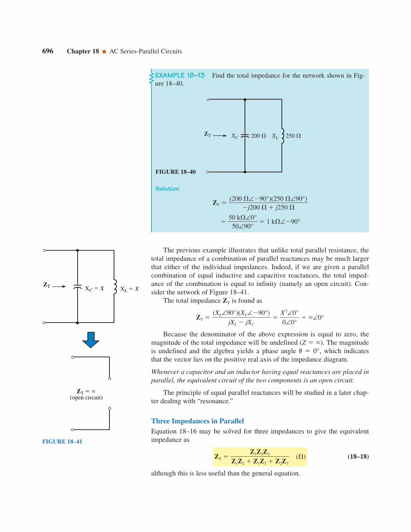
The previous example illustrates that unlike total parallel resistance, thetotal impedance of a combination of parallel reactances may be much largerthat either of the individual impedances. Indeed, if we are given a parallelcombination of equal inductive and capacitive reactances, the total imped-ance of the combination is equal to infinity (namely an open circuit). Con-sider the network of Figure 18–41.
The total impedance ZT is found as
ZT X
0
2
∠∠
0
0
°
° ∠0°
Because the denominator of the above expression is equal to zero, themagnitude of the total impedance will be undefined (Z ). The magnitudeis undefined and the algebra yields a phase angle v 0°, which indicatesthat the vector lies on the positive real axis of the impedance diagram.
Whenever a capacitor and an inductor having equal reactances are placed inparallel, the equivalent circuit of the two components is an open circuit.
The principle of equal parallel reactances will be studied in a later chap-ter dealing with “resonance.”
Three Impedances in ParallelEquation 18–16 may be solved for three impedances to give the equivalentimpedance as
ZT () (18–18)
although this is less useful than the general equation.
Z1Z2Z3Z1Z2 Z1Z3 Z2Z3
(XL∠90°)(XC∠90°)
jXL jXC
696 Chapter 18 AC Series-Parallel Circuits
EXAMPLE 18–13 Find the total impedance for the network shown in Fig-ure 18–40.
Solution
ZT
50
50k∠
9∠0°
0° 1 k∠90°
(200 ∠90°)(250 ∠90°)
j200 j250
FIGURE 18–40
ZT XC 200 XL 250
ZT XC X XL X
ZT (open circuit)
FIGURE 18–41

Section 18.4 AC Parallel Circuits 697
EXAMPLE 18–14 Find the equivalent impedance of the network of Figure18–42.
Solution
ZT
1.90 k∠18.43°
And so the equivalent impedance of the network is
ZT 1.80 k j0.6 k
12 109 ∠0°6.325 106∠18.43°
12 109 ∠0°6 106 j2 106
12 109 ∠0°6 106∠90° 4 106∠90° 6 106∠0°
(2 k∠0°)(3 k∠90°)(2 k∠90°)(2 k∠0°)(3 k∠90°) (2 k∠0°)(2 k∠90°) (3 k∠90°)(2 k∠90°)
ZT R 2 k XL 3 k XC 2 k
FIGURE 18–42
PRACTICEPROBLEMS 5
A circuit consists of a current source, i 0.030 sin 500t, in parallel with L 20 mH,C 50 mF, and R 25 .
a. Determine the voltage V across the circuit.
b. Solve for the power factor of the circuit.
c. Calculate the average power dissipated by the circuit and verify that this isequal to the power delivered by the source.
d. Use Ohm’s law to find the phasor quantities, IR, IL, and IC.
Answers:a. V 0.250 V∠61.93°
b. Fp 0.4705
c. PR 41.0 W PT
d. IR 9.98 mA∠61.98°
IC 6.24 mA∠151.93°
IL 25.0 mA∠28.07°
PRACTICEPROBLEMS 6
A circuit consists of a 2.5-Arms current source connected in parallel with a resis-tor, an inductor, and a capacitor. The resistor has a value of 10 and dissipates40 W of power.
a. Calculate the values of XL and XC if XL 3XC.
b. Determine the magnitudes of current through the inductor and the capacitor.
Answers:a. XL 80 , XC 26.7
b. IL 0.25 mA, IC 0.75 mA
698 Chapter 18 AC Series-Parallel Circuits
18.5 Kirchhoff’s Current Law and the Current Divider Rule
The current divider rule for ac circuits has the same form as for dc circuitswith the notable exception that currents are expressed as phasors. For a par-allel network as shown in Figure 18–43, the current in any branch of the net-work may be determined using either admittance or impedance.
Ix YY
T
xI or Ix
ZZ
T
x
I (18–19)
ZT Z2 Zx Zn
I1 I2 InIx
Z1
YT Y2 Yx YnY1
I
FIGURE 18–43
For two branches in parallel the current in either branch is determinedfrom the impedances as
I1 Z1
Z
2
Z2
I (18–20)
Also, as one would expect, Kirchhoff’s current law must apply to anynode within an ac circuit. For such circuits, KCL may be stated as fol-lows:
The summation of current phasors entering and leaving a node is equal tozero.
EXAMPLE 18–15 Calculate the current in each of the branches in the net-work of Figure 18–44.

Section 18.5 Kirchoff’s Current Law and the Current Divider Rule 699
Solution
I1 j220500
∠
j29500°
(2 A∠0°)
25500
∠∠
9900°°
(2 A∠0°) 10 A∠0°
and
I2 j202000
∠j29500°
(2 A∠0°)
52000
∠
∠
9900°°
(2 A∠0°) 8 A∠180°
The above results illustrate that the currents in parallel reactive compo-nents may be significantly larger than the applied current. If the currentthrough the component exceeds the maximum current rating of the element,severe damage may occur.
FIGURE 18–44
I 2 A∠0
XL 200 XC 250
I1 I2
EXAMPLE 18–16 Refer to the circuit of Figure 18–45:
ZT R 20 k XL 1 k XC 1 k
I1 I2 I3
IT a
E 5 V∠0
FIGURE 18–45

700 Chapter 18 AC Series-Parallel Circuits
a. Find the total impedance, ZT.
b. Determine the supply current, IT.
c. Calculate I1, I2, and I3 using the current divider rule.
d. Verify Kirchhoff’s current law at node a.
Solutiona. Because the inductive and capacitive reactances are in parallel and have
the same value, we may replace the combination by an open circuit. Con-sequently, only the resistor R needs to be considered. As a result
ZT 20 k∠0°
b. IT 20
5kV∠
∠0°
0° 250 mA∠0°
c. I1 2200
kk
∠∠
00°°
(250 mA∠0°) 250 mA∠0°
I2 210kk∠∠900°°
(250 mA∠0°) 5.0 mA∠90°
I3 12k0k∠
∠900°°
(250 mA∠0°) 5.0 mA∠90°
d. Notice that the currents through the inductor and capacitor are 180° out ofphase. By adding the current phasors in rectangular form, we have
IT 250 mA j5.0 A j5.0 A 250 mA j0 250 mA∠0°
The above result verifies Kirchhoff’s current law at the node.
1. Express Kirchhoff’s current law as it applies to ac circuits.
2. What is the fundamental difference between how Kirchhoff’s current law isapplied to ac circuits as compared with dc circuits?
(Answers are at the end of the chapter.)
IN-PROCESSLEARNINGCHECK 3
PRACTICEPROBLEMS 7
a. Use the current divider rule to determine current through each branch in thecircuit of Figure 18–46.
XL 40 R 30 XC 80
IL IR IC
250 µA∠0
FIGURE 18–46
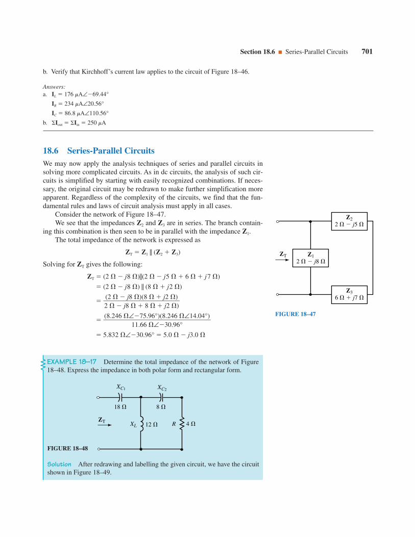
b. Verify that Kirchhoff’s current law applies to the circuit of Figure 18–46.
Answers:a. IL 176 mA∠69.44°
IR 234 mA∠20.56°
IC 86.8 mA∠110.56°
b. Iout Iin 250 mA
Section 18.6 Series-Parallel Circuits 701
18.6 Series-Parallel CircuitsWe may now apply the analysis techniques of series and parallel circuits insolving more complicated circuits. As in dc circuits, the analysis of such cir-cuits is simplified by starting with easily recognized combinations. If neces-sary, the original circuit may be redrawn to make further simplification moreapparent. Regardless of the complexity of the circuits, we find that the fun-damental rules and laws of circuit analysis must apply in all cases.
Consider the network of Figure 18–47.We see that the impedances Z2 and Z3 are in series. The branch contain-
ing this combination is then seen to be in parallel with the impedance Z1.The total impedance of the network is expressed as
ZT Z1 (Z2 Z3)
Solving for ZT gives the following:
ZT (2 j8 )(2 j5 6 j7 )
(2 j8 ) (8 j2 )
5.832 ∠30.96° 5.0 j3.0
(8.246 ∠75.96°)(8.246 ∠14.04°)
11.66 ∠30.96°
(2 j8 )(8 j2 )2 j8 8 j2 )
ZT
Z22 j5
Z36 j7
Z12 j8
FIGURE 18–47
EXAMPLE 18–17 Determine the total impedance of the network of Figure18–48. Express the impedance in both polar form and rectangular form.
FIGURE 18–48
XL 12 R 4
XC2
8
XC1
18
ZT
Solution After redrawing and labelling the given circuit, we have the circuitshown in Figure 18–49.

702 Chapter 18 AC Series-Parallel Circuits
The total impedance is given asZT Z1 Z2 Z3
where
Z1 j18 18∠90°
Z2 j12 12∠90°
Z3 4 j8 8.94 ∠63.43°
We determine the total impedance as
ZT j18
j18 1075.3.6
6∠
∠4256°.57°
j18 19.0 ∠18.43°
j18 18 j6
18 j24 30 ∠53.13°
(12 ∠90°)(8.94 ∠63.43°)
j12 4 j8
FIGURE 18–49
ZT Z3Z2
Z1
Z1 j18 Z2 j12 12 ∠90
Z3 4 j8 8.94 ∠63.43
EXAMPLE 18–18 Consider the circuit of Figure 18–50:
50 V∠0
2 k
1 k R2
XL
Z2
Z1
I1I2 I3
2 k XC Z3
R1
1 k
FIGURE 18–50

Section 18.6 Series-Parallel Circuits 703
a. Find ZT.
b. Determine the currents I1, I2, and I3.
c. Calculate the total power provided by the voltage source.
d. Determine the average powers P1, P2, and P3 dissipated by each of theimpedances. Verify that the average power delivered to the circuit is thesame as the power dissipated by the impedances.
Solutiona. The total impedance is determined by the combination
ZT Z1 Z2 Z3
For the parallel combination we have
Z2 Z3
4.472 k∠26.57° 4.0 k j2.0 k
And so the total impedance is
ZT 5 k j2 k 5.385 k∠21.80°
I1
9.285 mA∠21.80°
Applying the current divider rule, we get
I2
18.57 mA∠68.20°
and
I3
20.761 mA∠85.23°
c. PT (50 V)(9.285 mA)cos 21.80°
431.0 mW
d. Because only the resistors will dissipate power, we may use P I2R:
P1 (9.285 mA)2(1 k) 86.2 mW
P2 (18.57 mA)2(1 k) 344.8 mW
Alternatively, the power dissipated by Z2 may have been determined asP I2Z cos v:
P2 (18.57 mA)2(2.236 k)cos 63.43° 344.8 mW
(2.236 k∠63.43°)(9.285 mA∠21.80°)
1 k∠0°
(1 k j2 k)(9.285 mA∠21.80°)
1 k j2 k j2 k
(2 k∠90°)(9.285 mA∠21.80°)
1 k j2 k j2 k
50 V∠0°5.385 k∠21.80°
(2.236 k∠63.43°)(2 k∠90°)
1 k∠0°
(1 k j2 k)(j2 k)
1 k j2 k j2 k

18.7 Frequency EffectsAs we have already seen, the reactance of inductors and capacitors dependson frequency. Consequently, the total impedance of any network havingreactive elements is also frequency dependent. Any such circuit would need tobe analyzed separately at each frequency of interest. We will examine several
704 Chapter 18 AC Series-Parallel Circuits
Since Z3 is purely capacitive, it will not dissipate any power:
P3 0
By combining these powers, the total power dissipated is found:
PT 86.2 mW 344.8 mW 0 431.0 mW (checks!)
PRACTICEPROBLEMS 8
Refer to the circuit of Figure 18–51:
a. Calculate the total impedance, ZT.
b. Find the current I.
c. Use the current divider rule to find I1 and I2.
d. Determine the power factor for each impedance, Z1 and Z2.
e. Determine the power factor for the circuit.
f. Verify that the total power dissipated by impedances Z1 and Z2 is equal to thepower delivered by the voltage source.
Answers:a. ZT 18.9 ∠45°
b. I 1.06 A∠45°
c. I1 0.354 A∠135°, I2 1.12 A∠26.57°
d. FP(1) 0.4472 leading, FP(2) 0.7071 lagging
e. FP 0.7071 leading
f. PT 15.0 W, P1 2.50 W, P2 12.5 W
P1 P2 15.0 W PT
ZT Z1
I1
Z1 20 j40 Z2 10 j10
I2
I
20
Z2E 20 V∠0
FIGURE 18–51

fairly simple combinations of resistors, capacitors, and inductors to see howthe various circuits operate at different frequencies. Some of the moreimportant combinations will be examined in greater detail in later chapterswhich deal with resonance and filters.
RC CircuitsAs the name implies, RC circuits consist of a resistor and a capacitor. Thecomponents of an RC circuit may be connected either in series or in parallelas shown in Figure 18–52.
Section 18.7 Frequency Effects 705
R
C
(a) Series RC circuit (b) Parallel RC circuit
R C
FIGURE 18–52
Consider the RC series circuit of Figure 18–53.Recall that the capacitive reactance, XC, is given as
XC q
1C
2p
1fC
The total impedance of the circuit is a vector quantity expressed as
ZT R jq
1C R
jq1C
ZT 1
jqjCqRC (18–21)
If we define the cutoff or corner frequency for an RC circuit as
qc R1C
1t
(rad/s) (18–22)
or equivalently as
fc 2p
1RC (Hz) (18–23)
then several important points become evident.For q qc/10 (or f fc/10) Equation 18–21 can be expressed as
ZT 1
j
qCj0
jq
1C
and for q 10qc, the expression of (18–21) can be simplified as
ZT 0
jqjCqRC R
1 FC
1 kZT
R
FIGURE 18–53

Solving for the magnitude of the impedance at several angular frequen-cies, we have the results shown in Table 18–1.
If the magnitude of the impedance ZT is plotted as a function of angularfrequency q, we get the graph of Figure 18–54. Notice that the abscissa andordinate of the graph are not scaled linearly, but rather logarithmically. Thisallows for the the display of results over a wide range of frequencies.
706 Chapter 18 AC Series-Parallel Circuits
TABLE 18–1
AngularFrequency,
(Rad/s) XC () ZT ()
0 1 1 M 1 M10 100 k 100 k100 10 k 10.05 k200 5 k 5.099 k500 2 k 2.236 k1000 1 k 1.414 k2000 500 11185000 200 101910 k 100 1005100 k 10 1000
10 20 50 100 200 500 1000 2 k 5 k 10 k 20 k 50 k 100 k
100 k
10 k
1 k
ZT (Ω)
ω (rad/s)
FIGURE 18–54 Impedance versus angular frequency for the network of Figure 18–53.
The graph illustrates that the reactance of a capacitor is very high (effec-tively an open circuit) at low frequencies. Consequently, the total impedanceof the series circuit will also be very high at low frequencies. Secondly, wenotice that as the frequency increases, the reactance decreases. Therefore, asthe frequency gets higher, the capacitive reactance has a diminished effect inthe circuit. At very high frequencies (typically for q 10qc), the impedanceof the circuit will effectively be R 1 k.
Consider the parallel RC circuit of Figure 18–55. The total impedance,ZT, of the circuit is determined as
ZT Z
Z
R RZ
ZC
C
which may be simplified as
ZT 1
RjqRC (18–24)
jqRC
1
jqjCqRC
Rjq
1C
R jq
1C
C 1 F R 1 k
FIGURE 18–55

As before, the cutoff frequency is given by Equation 18–22. Now, byexamining the expression of (18–24) for q qc /10, we have the followingresult:
ZT 1
Rj0
R
For q 10qc, we have
ZT 0
RjqRC
jq1C
If we solve for the impedance of the circuit in Figure 18–55 at various angu-lar frequencies, we obtain the results of Table 18–2.
Plotting the magnitude of the impedance ZT as a function of angular fre-quency q, we get the graph of Figure 18–56. Notice that the abscissa andordinate of the graph are again scaled logarithmically, allowing for the dis-play of results over a wide range of frequencies.
Section 18.7 Frequency Effects 707
TABLE 18–2
AngularFrequency,
(Rad/s) XC () ZT ()
0 10001 1 M 100010 100 k 1000100 10 k 995200 5 k 981500 2 k 8941 k 1 k 7072 k 500 4475 k 200 19610 k 100 99.5100 k 10 10
ZT ()
2
20 50 100 200 5001
10
5
10
20
50
ω (rad/s)
ωC
100
200
500
1000
1 k 2 k 5 k 10 k 20 k 50 k100 k
FIGURE 18–56 Impedance versus angular frequency for the network of Figure 18–55.
The results indicate that at dc ( f 0 Hz) the capacitor, which behavesas an open circuit, will result in a circuit impedance of R 1 k. As the fre-quency increases, the capacitor reactance approaches 0 , resulting in a cor-responding decrease in circuit impedance.
RL CircuitsRL circuits may be analyzed in a manner similar to the analysis of RC cir-cuits. Consider the parallel RL circuit of Figure 18–57.
R 1 k XL 1 H
FIGURE 18–57
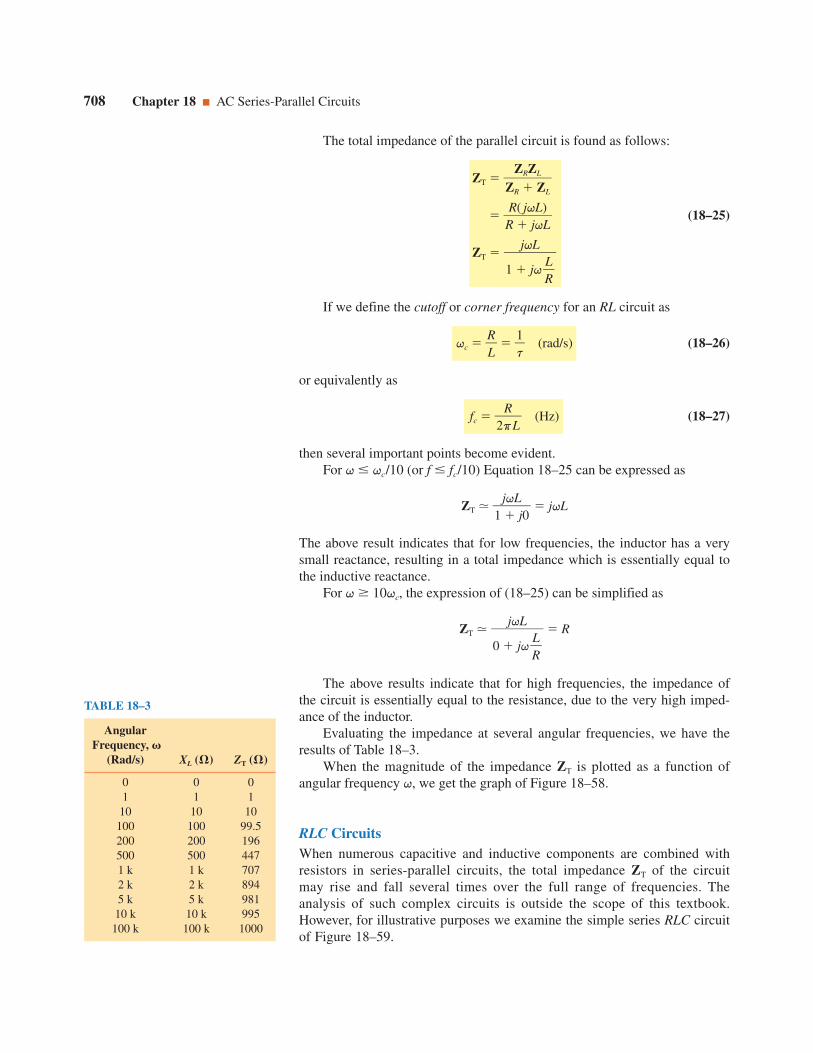
708 Chapter 18 AC Series-Parallel Circuits
TABLE 18–3
AngularFrequency,
(Rad/s) XL () ZT ()
0 0 01 1 110 10 10100 100 99.5200 200 196500 500 4471 k 1 k 7072 k 2 k 8945 k 5 k 98110 k 10 k 995100 k 100 k 1000
The total impedance of the parallel circuit is found as follows:
ZT Z
Z
R RZ
ZL
L
RR
( jqjqL)
L (18–25)
ZT
If we define the cutoff or corner frequency for an RL circuit as
qc RL
1t
(rad/s) (18–26)
or equivalently as
fc 2p
RL
(Hz) (18–27)
then several important points become evident.For q qc/10 (or f fc/10) Equation 18–25 can be expressed as
ZT 1
j
qLj0
jqL
The above result indicates that for low frequencies, the inductor has a verysmall reactance, resulting in a total impedance which is essentially equal tothe inductive reactance.
For q 10qc, the expression of (18–25) can be simplified as
ZT R
The above results indicate that for high frequencies, the impedance ofthe circuit is essentially equal to the resistance, due to the very high imped-ance of the inductor.
Evaluating the impedance at several angular frequencies, we have theresults of Table 18–3.
When the magnitude of the impedance ZT is plotted as a function ofangular frequency q, we get the graph of Figure 18–58.
RLC CircuitsWhen numerous capacitive and inductive components are combined withresistors in series-parallel circuits, the total impedance ZT of the circuitmay rise and fall several times over the full range of frequencies. Theanalysis of such complex circuits is outside the scope of this textbook.However, for illustrative purposes we examine the simple series RLC circuitof Figure 18–59.
jqL
0 jqRL
jqL
1 jqRL

The impedance ZT at any frequency will be determined as
ZT R jXL jXC
R j(XL XC)
At very low frequencies, the inductor will appear as a very low impedance(effectively a short circuit), while the capacitor will appear as a very highimpedance (effectively an open circuit). Because the capacitive reactancewill be much larger than the inductive reactance, the circuit will have a verylarge capacitive reactance. This results in a very high circuit impedance, ZT.
As the frequency increases, the inductive reactance increases, whilethe capacitive reactance decreases. At some frequency, f0, the inductor andthe capacitor will have the same magnitude of reactance. At this frequency,the reactances cancel, resulting in a circuit impedance which is equal to theresistance value.
As the frequency increases still further, the inductive reactance becomeslarger than the capacitive reactance. The circuit becomes inductive and themagnitude of the total impedance of the circuit again rises. Figure 18–60shows how the impedance of a series RLC circuit varies with frequency.
The complete analysis of the series RLC circuit and the parallel RLC cir-cuit is left until we examine the principle of resonance in a later chapter.
Section 18.7 Frequency Effects 709
ZT ()
2
1001
10
5
10
20
50
ω (rad/s)
100
200
500
1000
1 k 10 k 100 k
FIGURE 18–58 Impedance versus angular frequency for the network of Figure 18–57.
R
XL
XC
ZT
FIGURE 18–59
f (Hz)
ZT ()
fo
R
FIGURE 18–60
IN-PROCESSLEARNINGCHECK 4
1. For a series network consisting of a resistor and a capacitor, what will be theimpedance of the network at a frequency of 0 Hz (dc)? What will be theimpedance of the network as the frequency approaches infinity?
2. For a parallel network consisting of a resistor and an inductor, what will bethe impedance of the network at a frequency of 0 Hz (dc)? What will be theimpedance of the network as the frequency approaches infinity?
(Answers are at the end of the chapter.)

710 Chapter 18 AC Series-Parallel Circuits
PRACTICEPROBLEMS 9
Given the series RC network of Figure 18–61, calculate the cutoff frequency inhertz and in radians per second. Sketch the frequency response of ZT (magni-tude) versus angular frequency q for the network. Show the magnitude ZT atqc/10, qc, and 10qc.
Answers: qc 96.7 rad/s fc 15.4 HzAt 0.1 qc: ZT 472 k At qc: ZT 66.5 k At 10 qc: ZT 47.2 k
FIGURE 18–61 R
47 k
C 0.22 FZT
YT
ZT
RS
XS
FIGURE 18–62
RPYT
ZT XP
FIGURE 18–63
18.8 ApplicationsAs we have seen, we may determine the impedance of any ac circuit as a vec-tor Z R jX. This means that any ac circuit may now be simplified as aseries circuit having a resistance and a reactance, as shown in Figure 18–62.
Additionally, an ac circuit may be represented as an equivalent parallel circuitconsisting of a single resistor and a single reactance as shown in Figure 18–63.Any equivalent circuit will be valid only at the given frequency of operation.
We will now examine the technique used to convert any series impedanceinto its parallel equivalent. Suppose that the two circuits of Figure 18–62 andFigure 18–63 are exactly equivalent at some frequency. These circuits can beequivalent only if both circuits have the same total impedance, ZT, and thesame total admittance, YT.
From the circuit of Figure 18–62, the total impedance is written as
ZT RS jXS
Therefore, the total admittance of the circuit is
YT Z1
T
RS
1jXS
Multiplying the numerator and denominator by the complex conjugate,we obtain the following:
YT
R
R
S
S2
j
X
X
S
S2 (18–28)
YT RS
2
R
S
XS2 j
RS2
X
S
XS2
Now, from the circuit of Figure 18–63, the total admittance of the paral-lel circuit may be found from the parallel combination of RP and XP as
YT R1
P
1jXP
RS jXS(RS jXS)(RS jXS)

which gives
YT R1
P
jX1
P
(18–29)
Two vectors can only be equal if both the real components are equal and theimaginary components are equal. Therefore the circuits of Figure 18–62 andFigure 18–63 can only be equivalent if the following conditions are met:
RP RS
2
R
S
XS2
(18–30)
and
XP RS
2
X
S
XS2
(18–31)
In a similar manner, we have the following conversion from a parallelcircuit to an equivalent series circuit:
RS RP
R2
P
XP
X
2
P2 (18–32)
and
XS RP
R2
P
2X
XP
P2 (18–33)
Section 18.8 Applications 711
EXAMPLE 18–19 A circuit has a total impedance of ZT 10 j50 .Sketch the equivalent series and parallel circuits.
Solution The series circuit will be an inductive circuit having RS 10 and XLS 50 .
The equivalent parallel circuit will also be an inductive circuit having thefollowing values:
RP (10 )
1
2
0
(50 )2
260
XLP (10 )
5
2
0
(50 )2
52
The equivalent series and parallel circuits are shown in Figure 18–64.
RP
RS 10
50 XLS
260 XLP 52
FIGURE 18–64

712 Chapter 18 AC Series-Parallel Circuits
EXAMPLE 18–20 A circuit has a total admittance of YT 0.559 mS∠63.43°. Sketch the equivalent series and parallel circuits.
Solution Because the admittance is written in polar form, we first convertto the rectangular form of the admittance.
GP (0.559 mS) cos 63.43° 0.250 mS ⇔ RP 4.0 k
BCP (0.559 mS) sin 63.43° 0.500 mS ⇔ XCP 2.0 k
The equivalent series circuit is found as
RS (4
(k4k)2
)
(2(k2k)
2
)2 0.8 k
and
XCS (4
(k4k)2
)
2(2(2
kk
))2 1.6 k
The equivalent circuits are shown in Figure 18–65.
RP
RS 0.8 k
1.6 kXCS
4 kXCP 6 k
FIGURE 18–65
R2 30 k XL 10 k
R1
10 k
20 k
XC
ZT
200 V∠0
IT
FIGURE 18–66
EXAMPLE 18–21 Refer to the circuit of Figure 18–66.
a. Find ZT.
b. Sketch the equivalent series circuit.
c. Determine IT.
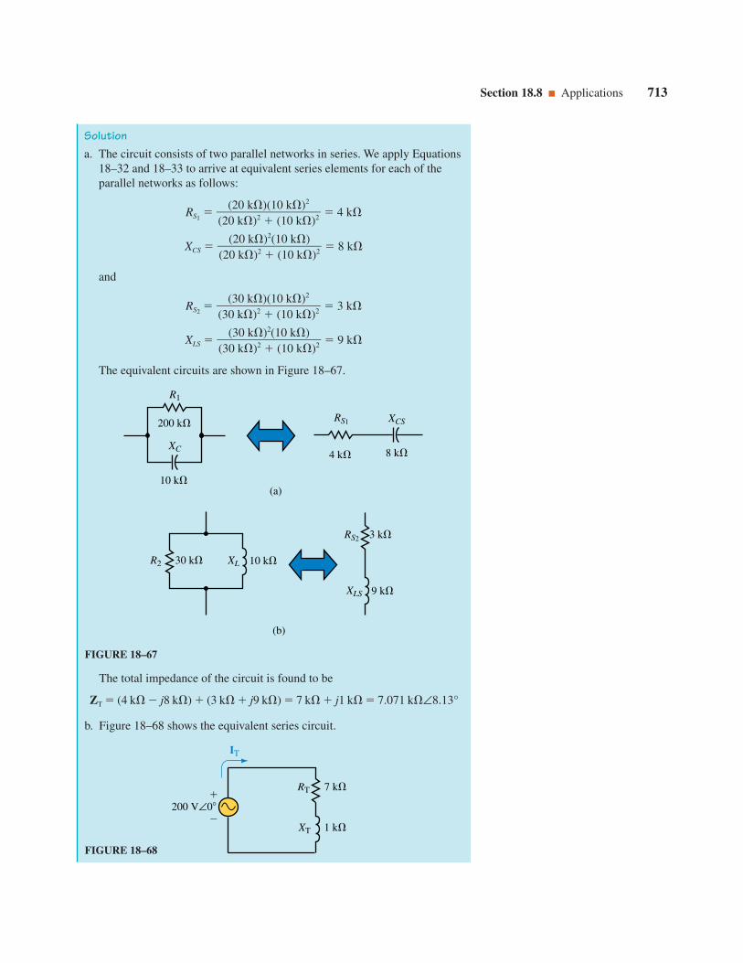
Section 18.8 Applications 713
Solutiona. The circuit consists of two parallel networks in series. We apply Equations
18–32 and 18–33 to arrive at equivalent series elements for each of theparallel networks as follows:
RS1 4 k
XCS 8 k
and
RS2 3 k
XLS 9 k
The equivalent circuits are shown in Figure 18–67.
(30 k)2(10 k)(30 k)2 (10 k)2
(30 k)(10 k)2
(30 k)2 (10 k)2
(20 k)2(10 k)(20 k)2 (10 k)2
(20 k)(10 k)2
(20 k)2 (10 k)2
R2
RS2 3 k
9 kXLS
30 k XL 10 k
10 k
XC
200 k
R1
RS1 XCS
4 k 8 k
(a)
(b)
FIGURE 18–67
The total impedance of the circuit is found to be
ZT (4 k j8 k) (3 k j9 k) 7 k j1 k 7.071 k∠8.13°
b. Figure 18–68 shows the equivalent series circuit.
FIGURE 18–68
1 k
200 V∠0
7 k RT
XT
IT

18.9 Circuit Analysis Using Computers
Electronics WorkbenchIn this section we will use Electronics Workbench to simulate how sinu-soidal ac measurements are taken with an oscilloscope. The “measurements”are then interpreted to verify the ac operation of circuits. You will use someof the display features of the software to simplify your work. The followingexample provides a guide through each step of the procedure.
714 Chapter 18 AC Series-Parallel Circuits
c. IT 7.07
2100
kV∠
∠08°.13°
28.3 mA∠8.13°
An inductor of 10 mH has a series resistance of 5 .
a. Determine the parallel equivalent of the inductor at a frequency of 1 kHz.Sketch the equivalent showing the values of LP (in henries) and RP.
b. Determine the parallel equivalent of the inductor at a frequency of 1 MHz.Sketch the equivalent showing the values of LP (in henries) and RP.
c. If the frequency were increased still further, predict what would happen to thevalues of LP and RP
(Answers are at the end of the chapter.)
IN-PROCESSLEARNINGCHECK 5
PRACTICEPROBLEMS 10
A network has an impedance of ZT 50 k∠75° at a frequency of 5 kHz.
a. Determine the most simple equivalent series circuit (L and R).
b. Determine the most simple equivalent parallel circuit.
Answers:a. RS 12.9 k, LS 1.54 H
b. RP 193 k, LP 1.65 H
ELECTRONICSWORKBENCH
PSpice
EXAMPLE 18–22 Given the circuit of Figure 18–69.
FIGURE 18–69
L 6.366 mH
30 R10 V∠0°
VR
I
1000 Hz

Section 18.9 Circuit Analysis Using Computers 715
a. Determine the current I and the voltage VR.
b. Use Electronics Workbench to display the resistor voltage vR and thesource voltage e. Use the results to verify the results of part (a).
Solutiona. XL 2p(1000 Hz)(6.366 103 H) 40
Z 30 j40 50 ∠53.13°
I 50
10
∠V
5∠30.1°3°
0.200 A∠53.13°
VR (0.200 A∠53.13°)(30 ) 6.00 V∠53.13°
b. Use the schematic editor to input the circuit shown in Figure 18–70.
The ac voltage source is obtained from the Sources parts bin. The proper-ties of the voltage source are changed by double clicking on the symboland then selecting the Value tab. Change the values as follows:
Voltage (V): 10 V
Frequency: 1 kHz
Phase: 0 Deg
The oscilloscope is selected from the Instruments parts bin and the settingsare changed as follows:
Time base: 0.2 ms/div
Channel A: 5 V/Div
Channel B: 5 V/Div
EWB FIGURE 18–70

716 Chapter 18 AC Series-Parallel Circuits
At this point, the circuit could be simulated and the display will resembleactual lab results. However, we can refine the display to provide informa-tion that is more useful. First, click on Analysis/Options. Next click on theInstruments tab and change the following settings for the oscilloscope:
Pause after each screen
•Minimum number of time points 1000
After returning to the main window, click on the Power switch. It is neces-sary to press the Pause/Resume button once, since the display on the oscil-loscope will not immediately show the circuit steady state values, butrather begins from t 0. Consequently the display will show the transient(which in this case will last approximately 5 L/R 1 ms).
Now, we can obtain a more detailed display by clicking on the DisplayGraphs button. We will use cursors and a grid to help in the analysis. The dis-play will show several cycles of selected voltages. However, we are reallyonly interested in viewing one complete cycle. This is done as follows:
Click on the Properties button. Select the General tab. We enable thecursors by selecting • All traces and Cursors On from the Cursors box.Next, we enable the grid display by selecting Grid On from the Grid box.
The abscissa (time axis) is adjusted to show one period from t 4 msto t 5 ms by selecting the Bottom Axis tab and adjusting the values asfollows:
Range Minimum 0.004
Maximum 0.005
Divisions Number 20
The resulting display is shown in Figure 18–71.
FIGURE 18–71

OrCAD PSpiceIn the following example we will use the Probe postprocessor of PSpice toshow how the impedance of an RC circuit changes as a function of fre-quency. The Probe output will provide a graphical result that is very similarto the frequency responses determined in previous sections of this chapter.
Section 18.9 Circuit Analysis Using Computers 717
After positioning the cursors and using the display window, we are able toobtain various measurements for the circuit. The phase angle of the resis-tor voltage with respect to the source voltage is found by using the differ-ence between the cursors in the bottom axis, dx 146.88 ms. Now wehave
v 114060.808m
m
ss
360° 52.88°
The amplitude of the resistor voltage is 8.49 V, which results in an rmsvalue of 6.00 V. As a result of the measurements we have
VR 6.00 V∠52.88°
and
I 6 V∠
3
052.88° 0.200 A∠52.88°
These values correspond very closely to the theoretical results calculatedin part (a) of the example.
EXAMPLE 18–23 Refer to the network of Figure 18–72. Use the OrCADCapture CIS Demo to input the circuit. Run the Probe postprocessor to pro-cide a graphical display of network impedance as a function of frequencyfrom 50 Hz to 500 Hz.
FIGURE 18–72
R1
1 k
1 FZT C
Solution Since PSpice is unable to analyze an incomplete circuit, it is nec-essary to provide a voltage source (and ground) for the circuit of Figure 18–72.The input impedance is not dependent on the actual voltage used, and so wemay use any ac voltage source. In this example we arbitrarily select a voltageof 10 V.
• Open the CIS Demo software.
• Open a new project and call it Ch 18 PSpice 1. Ensure that the Analog orMixed-Signal Circuit Wizard is activated.

718 Chapter 18 AC Series-Parallel Circuits
• Enter the circuit as show in Figure 18–73. Simply click on the voltagevalue and change its value to 10V from the default value of 0V. (Theremust be no spaces between the magnitude and the units.
FIGURE 18–73
• Click on PSpice, New Simulation Profile and give a name such as Example18-23 to the new simulation. The Simulation Settings dialog box will open.
• Click on the Analysis tab and select AC Sweep/Noise as the Analysis type.Select General Settings from the Options box.
• Select Linear AC Sweep Type (Quite often, logarithmic frequency sweepssuch as Decade, are used). Enter the following values into the appropriatedialog boxes. Start Frequency; 50, End Frequency: 500, Total Points: 1001.Click OK.
• Click on PSpice and Run. The Probe postprocessor will appear on thescreen.
• Click on Trace and Add Trace. You may simply click on the appropriatevalues from the list of variables and use the division symbol to result inimpedance. Enter the following expression into the Trace Expression box:
V(R1:1)/I(R1)
Notice that the above expression is nothing other than an application ofOhm’s Law. The resulting display is shown in Figure 18–74.

a. Determine the current I and the voltage VR.
b. Use Electronics Workbench to display the resistor voltage vR and the sourcevoltage, e. Use the results to verify the results of part (a).
Answers:a. I 2.00 mA∠36.87°, VR 8.00 V∠36.87°
b. vR 11.3 sin(qt 36.87°), e 14.1 sin qt
Section 18.9 Circuit Analysis Using Computers 719
FIGURE 18–74
PRACTICEPROBLEMS 11
EWB Given the circuit of Figure 18–75.
C 0.5305 µF
4k 100 Hz
R10 V∠0°
VR
I
FIGURE 18–75

18.1 Ohm’s Law for AC Circuits
1. For the resistor shown in Figure 18–76:
a. Find the sinusoidal current i using phasors.
b. Sketch the sinusoidal waveforms for v and i.
c. Sketch the phasor diagram for V and I.
720 Chapter 18 AC Series-Parallel Circuits
PUTTING IT INTO PRACTICE
You are working in a small industrial plant where several small motors arepowered by a 60-Hz ac line voltage of 120 Vac. Your supervisor tells you
that one of the 2-Hp motors which was recently installed draws too much cur-rent when the motor is under full load. You take a current reading and findthat the current is 14.4 A. After doing some calculations, you determine thateven if the motor is under full load, it shouldn’t require that much current.
However, you have an idea. You remember that a motor can be repre-sented as a resistor in series with an inductor. If you could reduce the effect ofthe inductive reactance of the motor by placing a capacitor across the motor,you should be able to reduce the current since the capacitive reactance willcancel the inductive reactance.
While keeping the motor under load, you place a capacitor into the cir-cuit. Just as you suspected, the current goes down. After using several differ-ent values, you observe that the current goes to a minimum of 12.4 A. It is atthis value that you have determined that the reactive impedances are exactlybalanced. Sketch the complete circuit and determine the value of capacitancethat was added into the circuit. Use the information to determine the value ofthe motor’s inductance. (Assume that the motor has an efficiency of 100%.)
PROBLEMS
200
v 25 sinωt
i
6 k
v
I 30 mA∠40
FIGURE 18–76 FIGURE 18–77
2. Repeat Problem 1 for the resistor of Figure 18–77.
3. Repeat Problem 1 for the resistor of Figure 18–78.
PRACTICEPROBLEMS 12
PSpice Use OrCAD PSpice to input the circuit of Figure 18–55. Use theProbe postprocessor to obtain a graphical display of the network impedance as afunction of frequency from 100 Hz to 2000 Hz.

4. Repeat Problem 1 for the resistor of Figure 18–79.
5. For the component shown in Figure 18–80:
a. Find the sinusoidal voltage v using phasors.
b. Sketch the sinusoidal waveforms for v and i.
c. Sketch the phasor diagram for V and I.
Problems 721
47 k
V 62 V∠30
i
33
v
i 10 sin(ωt 60)
FIGURE 18–78 FIGURE 18–79
680
v
i 2.0 10–3 sinωt
5 k
i
v 2.3 sin(ωt 120)
FIGURE 18–80 FIGURE 18–81
6. Repeat Problem 5 for the component shown in Figure 18–81.
7. Repeat Problem 5 for the component shown in Figure 18–82.
L 30 mH
v
I 5 A∠ 60
f 1 kHz C 0.47 F
V 200 mV∠90
i
f 1 kHz
FIGURE 18–82 FIGURE 18–83
8. Repeat Problem 5 for the component shown in Figure 18–83.
9. Repeat Problem 5 for the component shown in Figure 18–84.
0.01 F
v C
i 6.25 10–3 sin 10 000 t
FIGURE 18–84

10. Repeat Problem 5 for the component shown in Figure 18–85.
722 Chapter 18 AC Series-Parallel Circuits
i
v 8 cos(200t 30)L 240 H
150 mH
i 22.5 10–3 cos(20 000 t 20)
v L
FIGURE 18–85 FIGURE 18–86
11. Repeat Problem 5 for the component shown in Figure 18–86.
12. Repeat Problem 5 for the component shown in Figure 18–87.
0.0033 F
i
C v 170 sin(377t 40)
FIGURE 18–87
18.2 AC Series Circuits
13. Find the total impedance of each of the networks shown in Figure 18–88.
R
30
25 ZT XC
XL
35
(a)
ZT 3.3 k
3 k 1.5 k
4.2 k5.9 k
XL
R1
R2
XC1
XC2
(b)
FIGURE 18–88
14. Repeat Problem 13 for the networks of Figure 18–89.
15. Refer to the network of Figure 18–90.
a. Determine the series impedance Z which will result in the given totalimpedance, ZT. Express your answer in rectangular and polar form.
b. Sketch an impedance diagram showing ZT and Z.
16. Repeat Problem 15 for the network of Figure 18–91.
17. A circuit consisting of two elements has a total impedance of ZT 2 k∠15°at a frequency of 18 kHz. Determine the values in ohms, henries, or faradsof the unknown elements.

Problems 723
ZT
Z1
30 j40
Z280 ∠60
(a)
ZT
Z1
30 ∠20°
Z255 ∠−30°
Z320 ∠−90
(b)
FIGURE 18–89
ZT 100 ∠30
R
47
36 XL
Z
ZT 90 ∠25
Z1
16 ∠30
Z
R 25
FIGURE 18–90 FIGURE 18–91
18. A network has a total impedance of ZT 24.0 k∠30° at a frequency of2 kHz. If the network consists of two series elements, determine the valuesin ohms, henries, or farads of the unknown elements.
19. Given that the network of Figure 18–92 is to operate at a frequency of 1 kHz,what series components R and L (in henries) or C (in farads) must be in theindicated block to result in a total circuit impedance of ZT 50 ∠60°?
20. Repeat Problem 19 for a frequency of 2 kHz.
21. Refer to the circuit of Figure 18–93.
a. Find ZT, I, VR, VL, and VC.
b. Sketch the phasor diagram showing I, VR, VL, and VC.
ZT 50 ∠60
L
20 mH
10 R
Z
FIGURE 18–92XL
20
50 XC
E 120 V∠0
I
VL
VR
40
R
VCZT
FIGURE 18–93

c. Determine the average power dissipated by the resistor.
d. Calculate the average power delivered by the voltage source. Comparethe result to (c).
22. Consider the circuit of Figure 18–94.
a. Find ZT, I, VR, VL, and VC.
b. Sketch the phasor diagram showing I, VR, VL, and VC.
c. Write the sinusoidal expressions for the current i and the voltages e, vR,vC, and vL.
d. Sketch the sinusoidal current and voltages found in (c).
e. Determine the average power dissipated by the resistor.
f. Calculate the average power delivered by the voltage source. Comparethe result to (e).
724 Chapter 18 AC Series-Parallel Circuits
R
4 k
6 kXL
E 10 V∠0
I
VR
VC
3 k
XC
VL
XL
47
36
XC
e 24 sin(ωt)
i
vC
vL
20
R
vRZT
FIGURE 18–94 FIGURE 18–95
23. Refer to the circuit of Figure 18–95.
a. Determine the circuit impedance, ZT.
b. Use phasors to solve for i, vR, vC, and vL.
c. Sketch the phasor diagram showing I, VR, VL, and VC.
d. Sketch the sinusoidal expressions for the current and voltages found in (b).
e. Determine the average power dissipated by the resistor.
f. Calculate the average power delivered by the voltage source. Comparethe result to (e).
24. Refer to the circuit of Figure 18–96.
a. Determine the value of the capacitor reactance, XC, needed so that theresistor in the circuit dissipates a power of 200 mW.
b. Using the value of XC from (a), determine the sinusoidal expression forthe current i in the circuit.
18.3 Kirchhoff’s Voltage Law and the Voltage Divider Rule
25. a. Suppose a voltage of 10 V∠0° is applied across the network in Figure18–88a. Use the voltage divider rule to find the voltage appearing acrosseach element.
b. Verify Kirchhoff’s voltage law for each network.
R
100
XC
e 10 sin(ωt)
i
50
XL
P 200 mW
FIGURE 18–96

26. a. Suppose a voltage of 240 V∠30° is applied across the network in Figure18–89a. Use the voltage divider rule to find the voltage appearing acrosseach impedance.
b. Verify Kirchhoff’s voltage law for each network.
27. Given the circuit of Figure 18–97:
a. Find the voltages VC and VL.
b. Determine the value of R.
Problems 725
XL
63.3
VR 125 V∠60
XC
E 250 V∠0
VC
VL
20
R
XL
400
XC
E 120 V∠0
VL
VR
50
R
VC 118.8 V∠45
FIGURE 18–97 FIGURE 18–98
28. Refer to the circuit of Figure 18–98.
a. Find the voltages VR and VL.
b. Determine the value of XC.
29. Refer to the circuit of Figure 18–99:
a. Find the voltage across XC.
b. Use Kirchhoff’s voltage law to find the voltage across the unknownimpedance.
c. Calculate the value of the unknown impedance Z.
d. Determine the average power dissipated by the circuit.
R
20
E 10 V∠30
VR 4 V∠20
VC
30
XC
VZZ
FIGURE 18–99
R1
100
E 600 V∠30
VR
VL
200
XL
VZZ
PT 500 WI 2 A∠θ
FIGURE 18–100
30. Given that the circuit of Figure 18–100 has a current with a magnitude of2.0 A and dissipates a total power of 500 W:
a. Calculate the value of the unknown impedance Z. (Hint: Two solutionsare possible.)
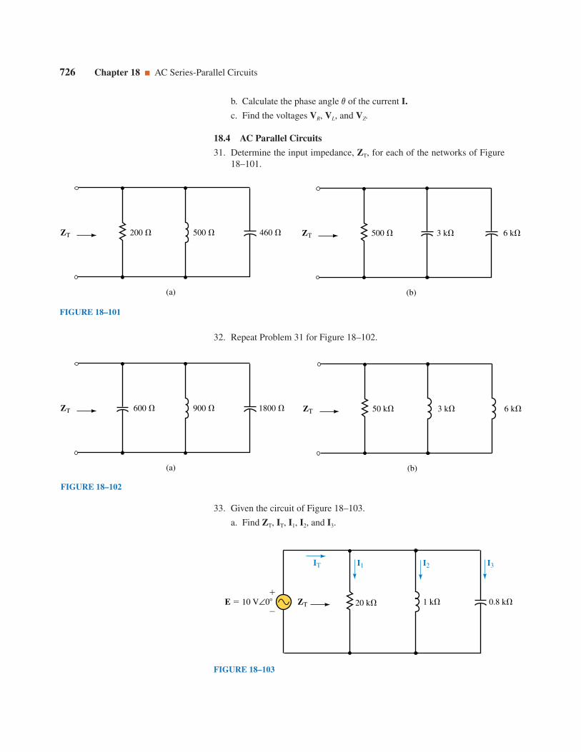
b. Calculate the phase angle v of the current I.
c. Find the voltages VR, VL, and VZ.
18.4 AC Parallel Circuits
31. Determine the input impedance, ZT, for each of the networks of Figure18–101.
726 Chapter 18 AC Series-Parallel Circuits
ZT 200 500 460
(a) (b)
ZT 500 3 k 6 k
FIGURE 18–101
32. Repeat Problem 31 for Figure 18–102.
ZT 600 900 1800
(a) (b)
ZT 50 k 3 k 6 k
FIGURE 18–102
33. Given the circuit of Figure 18–103.
a. Find ZT, IT, I1, I2, and I3.
ZT 20 k 1 k 0.8 k
I1 I2 I3IT
E 10 V∠0
FIGURE 18–103

b. Sketch the admittance diagram showing each of the admittances.
c. Sketch the phasor diagram showing E, IT, I1, I2, and I3.
d. Determine the average power dissipated by the resistor.
e. Find the power factor of the circuit and calculate the average powerdelivered by the voltage source. Compare the answer with the resultobtained in (d).
34. Refer to the circuit of Figure 18–104.
a. Find ZT, IT, I1, I2, and I3.
b. Sketch the admittance diagram for each of the admittances.
c. Sketch the phasor diagram showing E, IT, I1, I2, and I3.
d. Determine the expressions for the sinusoidal currents iT, i1, i2, and i3.
e. Sketch the sinusoidal voltage e and current iT.
f. Determine the average power dissipated by the resistor.
g. Find the power factor of the circuit and calculate the average powerdelivered by the voltage source. Compare the answer with the resultobtained in (f).
Problems 727
ZT 25 k 1 F 20 mH
I1 I2 I3IT
e 50 sin(10 000t) R C L
FIGURE 18–104
35. Refer to the network of Figure 18–105.
a. Determine ZT.
b. Given the indicated current, use Ohm’s law to find the voltage, V, acrossthe network.
ZT Z13 k j4 k
Z13 k j8 k
V
I 30 mA∠0
FIGURE 18–105

36. Consider the network of Figure 18–106.
a. Determine ZT.
b. Given the indicated current, use Ohm’s law to find the voltage, V, acrossthe network.
c. Solve for I2 and I.
728 Chapter 18 AC Series-Parallel Circuits
ZT 4 ∠60Z1
2 j5 Z2
FIGURE 18–107
ZT 1.2 k∠0Z1
3 k j1 kZ2
FIGURE 18–108
38. Determine the impedance, Z2, which will result in the total impedanceshown in Figure 18–108.
18.5 Kirchhoff’s Current Law and the Current Divider Rule
39. Solve for the current in each element of the networks in Figure 18–101 ifthe current applied to each network is 10 mA∠30°.
40. Repeat Problem 39 for Figure 18–102.
41. Use the current divider rule to find the current in each of the elements inFigure 18–109. Verify that Kirchhoff’s current law applies.
42. Given that IL 4 A∠30° in the circuit of Figure 18–110, find the currents I,IC, and IR. Verify that Kirchhoff’s current law appplies for this circuit.
43. Suppose that the circuit of Figure 18–111 has a current I with a magnitudeof 8 A:
a. Determine the current IR through the resistor.
b. Calculate the value of resistance, R.
c. What is the phase angle of the current I?
ZT Z130 j60
Z210 j40
V
I
I1 100 mA∠30 I2
FIGURE 18–106
37. Determine the impedance, Z2, which will result in the total impedanceshown in Figure 18–107.
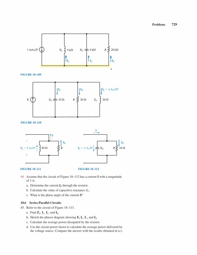
Problems 729
XL 5 k R4 kXC 20 k
IL IC IR
1 mA∠0
a
FIGURE 18–109
XL10 R 20 XC 20
IR IL 4 A∠30IC
I
FIGURE 18–110
I
50 R
IR
IL 5 A∠0
I
XC R
IR
IC 2 A∠0 10
FIGURE 18–111 FIGURE 18–112
44. Assume that the circuit of Figure 18–112 has a current I with a magnitudeof 3 A:
a. Determine the current IR through the resistor.
b. Calculate the value of capacitive reactance XC.
c. What is the phase angle of the current I?
18.6 Series-Parallel Circuits
45. Refer to the circuit of Figure 18–113.
a. Find ZT, IL , IC, and IR.
b. Sketch the phasor diagram showing E, IL, IC, and IR.
c. Calculate the average power dissipated by the resistor.
d. Use the circuit power factor to calculate the average power delivered bythe voltage source. Compare the answer with the results obtained in (c).

730 Chapter 18 AC Series-Parallel Circuits
20 V∠0
9 k
3 k
30 k ZT
8 k
I2 I3
V
I1
4 k
FIGURE 18–114
46. Refer to the circuit of Figure 18–114.
a. Find ZT, I1, I2, and I3.
b. Sketch the phasor diagram showing E, I1, I2, and I3.
c. Calculate the average power dissipated by each of the resistors.
d. Use the circuit power factor to calculate the average power delivered bythe voltage source. Compare the answer with the results obtained in (c).
20 V∠0
2
6 4
ZT
3
I1 I2
IT
6
Vab
a b
FIGURE 18–115
47. Refer to the circuit of Figure 18–115.
a. Find ZT, IT, I1, and I2.
b. Determine the voltage Vab.
XC 30 60
IL
E 120 V∠0
IC IR
5
XL
VRR
FIGURE 18–113

48. Consider the circuit of Figure 18–116.
a. Find ZT, IT, I1, and I2.
b. Determine the voltage V.
Problems 731
20 40
30 1
ZT
10
5 V∠0 V
I1I2IT
FIGURE 18–116
ZT 10 k 10 k
9 k
I1
I2
I3
1 mA∠0 R1 XC
XL
3 kR2
V
FIGURE 18–117
49. Refer to the circuit of Figure 18–117:
a. Find ZT, I1, I2, and I3.
b. Determine the voltage V.
400 k 50 k 40 k
I1 I2
R2 = 20 k
1 A∠0 R1 XC XL
I3
V
FIGURE 18–118
50. Refer to the circuit of Figure 18–118:
a. Find ZT, I1, I2, and I3.
b. Determine the voltage V.

18.7 Frequency Effects
51. A 50-k resistor is placed in series with a 0.01-mF capacitor. Determine thecutoff frequency qC (in rad/s) and sketch the frequency response (ZT vs. q)of the network.
52. A 2-mH inductor is placed in parallel with a 2-k resistor. Determine thecutoff frequency qC (in rad/s) and sketch the frequency response (ZT vs. q)of the network.
53. A 100-k resistor is placed in parallel with a 0.47-mF capacitor. Determinethe cutoff frequency fC (in Hz) and sketch the frequency response (ZT vs. f )of the network.
54. A 2.7-k resistor is placed in parallel with a 20-mH inductor. Determine thecutoff frequency fC (in Hz) and sketch the frequency response (ZT vs. f ) ofthe network.
18.8 Applications
55. Convert each each of the networks of Figure 18–119 into an equivalentseries network consisting of two elements.
732 Chapter 18 AC Series-Parallel Circuits
(a)
30 k 10 k
2.5 k
(b)
90
270
300
FIGURE 18–119
(a) (b)
100 10 F
100 mH100
R
L
C
R
R
100
FIGURE 18–120
56. Convert each each of the networks of Figure 18–119 into an equivalent par-allel network consisting of two elements.
57. Show that the networks of Figure 18–120 have the same input impedance atfrequencies of 1 krad/s and 10 krad/s. (It can be shown that these networksare equivalent at all frequencies.)

58. Show that the networks of Figure 18–121 have the same input impedance atfrequencies of 5 rad/s and 10 rad/s.
Problems 733
25 H 50
150
ZT
(a) (b)
100
100
100
ZT
100 H
FIGURE 18–121
398 µF
3 R
C
VR
100 Hz 20 V∠0°
VC
EWB FIGURE 18–122
18.9 Circuit Analysis Using Computers
59. EWB Given the circuit of Figure 18–122:
a. Use Electronics Workbench to simultaneously display the capacitor volt-age vC and e. Record your results and determine the phasor voltage VC.
b. Interchange the positions of the resistor and the capacitor relative to theground. Use Electronics Workbench to simultaneously display the resistorvoltage vR and e. Record your results and determine the phasor voltage VR.
c. Compare your results to those obtained in Example 18–8.
60. EWB Given the circuit of Figure 18–123:
a. Use Electronics Workbench to display the inductor voltage vL and e.Record your results and determine the phasor voltage VL.
b. Interchange the positions of the resistor and the inductor relative to theground. Use Electronics Workbench to display the inductor voltage vR
and e. Record your results and determine the phasor voltage VR.
c. Compare your results to those obtained in Example 18–9.
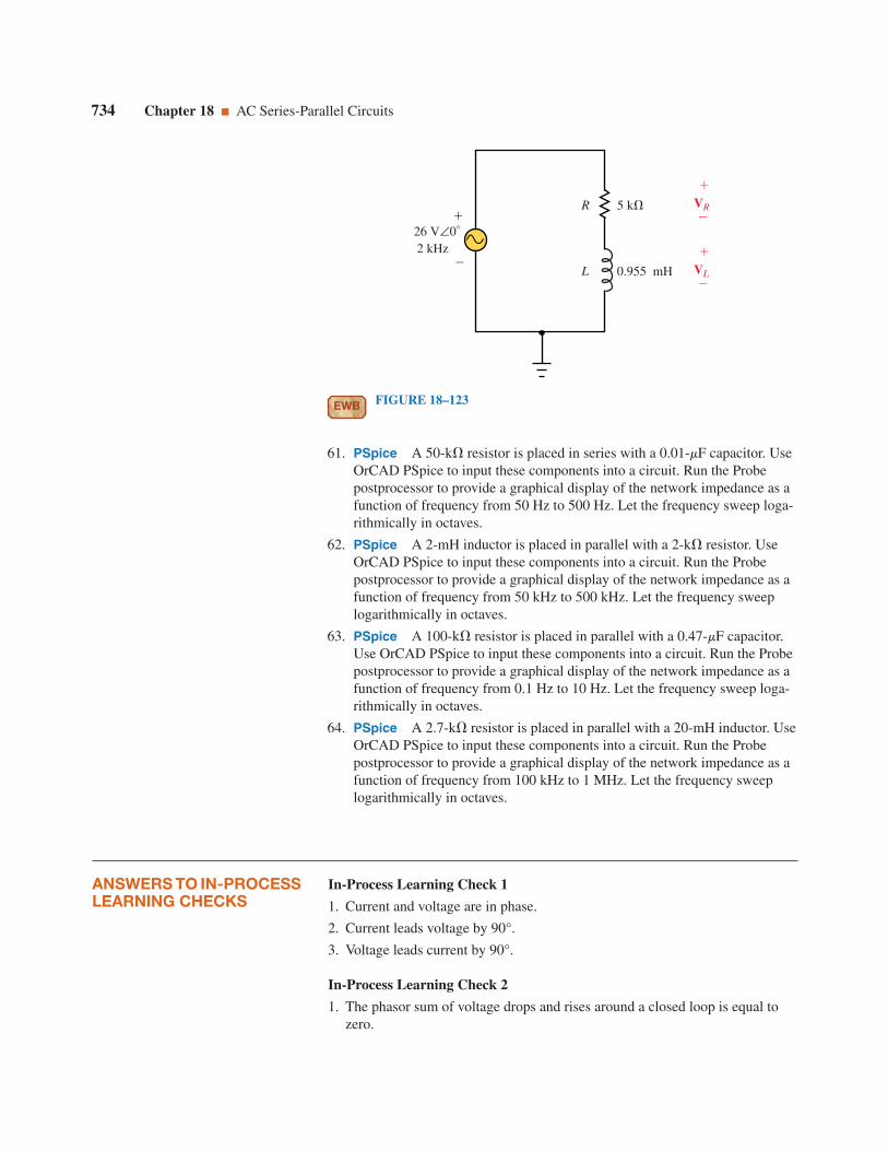
61. PSpice A 50-k resistor is placed in series with a 0.01-mF capacitor. UseOrCAD PSpice to input these components into a circuit. Run the Probepostprocessor to provide a graphical display of the network impedance as afunction of frequency from 50 Hz to 500 Hz. Let the frequency sweep loga-rithmically in octaves.
62. PSpice A 2-mH inductor is placed in parallel with a 2-k resistor. UseOrCAD PSpice to input these components into a circuit. Run the Probepostprocessor to provide a graphical display of the network impedance as afunction of frequency from 50 kHz to 500 kHz. Let the frequency sweeplogarithmically in octaves.
63. PSpice A 100-k resistor is placed in parallel with a 0.47-mF capacitor.Use OrCAD PSpice to input these components into a circuit. Run the Probepostprocessor to provide a graphical display of the network impedance as afunction of frequency from 0.1 Hz to 10 Hz. Let the frequency sweep loga-rithmically in octaves.
64. PSpice A 2.7-k resistor is placed in parallel with a 20-mH inductor. UseOrCAD PSpice to input these components into a circuit. Run the Probepostprocessor to provide a graphical display of the network impedance as afunction of frequency from 100 kHz to 1 MHz. Let the frequency sweeplogarithmically in octaves.
734 Chapter 18 AC Series-Parallel Circuits
ANSWERS TO IN-PROCESSLEARNING CHECKS
In-Process Learning Check 1
1. Current and voltage are in phase.
2. Current leads voltage by 90°.
3. Voltage leads current by 90°.
In-Process Learning Check 2
1. The phasor sum of voltage drops and rises around a closed loop is equal tozero.
0.955 mH
5 kR
L
VR
2 kHz 26 V∠0°
VL
EWB FIGURE 18–123
2. All voltages must be expressed as phasors, i.e., V V∠v V cos v jV sin v.
In-Process Learning Check 3
1. The phasor sum of currents entering a node is equal to the phasor sum of cur-rents leaving the same node.
2. All currents must be expressed as phasors, i.e., I I∠v I cos v jI sin v.
In-Process Learning Check 4
1. At f 0 Hz, Z (open circuit)
2. As f → , Z R
In-Process Learning Check 5
1. RP 795 , LP 10.1 mH
2. RP 790 M, LP 10.0 mH
Answers to In-Process Learning Checks 735

OBJECTIVES
After studying this chapter, you will beable to
• convert an ac voltage source into itsequivalent current source, and con-versely, convert a current source into anequivalent voltage source,
• solve for the current or voltage in a cir-cuit having either a dependent currentsource or a dependent voltage source,
• set up simultaneous linear equations tosolve an ac circuit using mesh analysis,
• use complex determinants to find thesolutions for a given set of linear equa-tions,
• set up simultaneous linear equations tosolve an ac circuit using nodal analysis,
• perform delta-to-wye and wye-to-deltaconversions for circuits having reactiveelements,
• solve for the balanced condition in agiven ac bridge circuit. In particular, youwill examine the Maxwell, Hay, andSchering bridges,
• use Electronics Workbench to analyzebridge circuits,
• use PSpice to calculate current and volt-age in an ac circuit.
KEY TERMS
Balanced Bridges
Controlling Elements
Delta-Wye Conversion
Dependent Sources
Hay Bridge
Maxwell Bridge
Mesh Analysis
Nodal Analysis
Schering Bridge
Source Conversion
OUTLINE
Dependent Sources
Source Conversion
Mesh (Loop) Analysis
Nodal Analysis
Delta-to-Wye and Wye-to-Delta Conver-sions
Bridge Networks
Circuit Analysis Using Computers
Methods of AC Analysis19

To this point, we have examined only circuits having a single ac source. Inthis chapter, we continue our study by analyzing multisource circuits and
bridge networks. You will find that most of the techniques used in analyzing accircuits parallel those of dc circuit analysis. Consequently, a review of Chapter 8will help you understand the topics of this chapter.
Near the end of the chapter, we examine how computer techniques are usedto analyze even the most complex ac circuits. It must be emphasized thatalthough computer techniques are much simpler than using a pencil and calcula-tor, there is virtually no knowledge to be gained by mindlessly entering data intoa computer. We use the computer merely as a tool to verify our results and toprovide a greater dimension to the analysis of circuits.
737
CHAPTER PREVIEW
PUTTING IT INPERSPECTIVE
Hermann Ludwig Ferdinand von Helmholtz
HERMANN HELMHOLTZ WAS BORN IN POTSDAM (near Berlin, Germany) onAugust 31, 1821. Helmholtz was a leading scientist of the nineteenth century,whose legacy includes contributions in the fields of acoustics, chemistry, mathe-matics, magnetism, electricity, mechanics, optics, and physiology.
Helmholtz graduated from the Medical Institute in Berlin in 1843 and prac-ticed medicine for five years as a surgeon in the Prussian army. From 1849 to1871, he served as a professor of physiology at universities in Königsberg,Bonn, and Heidelberg. In 1871, Helmholtz was appointed Professor of Physicsat the University of Berlin.
Helmholtz’ greatest contributions were as a mathematical physicist, wherehis work in theoretical and practical physics led to the proof of the Law of Con-servation of Energy in his paper “Über die Erhaltung der Kraft,” published in1847. He showed that mechanics, heat, light, electricity, and magnetism weresimply manifestations of the same force. His work led to the understanding ofelectrodynamics (the motion of charge in conductors), and his theory of the elec-tromagnetic properties of light set the groundwork for later scientists to under-stand how radio waves are propagated.
For his work, the German emperor Kaiser Wilhelm I made Helmholtz anoble in 1883. This great scientist died on September 8, 1894, at the age of 73.

19.1 Dependent SourcesThe voltage and current sources we have worked with up to now have beenindependent sources, meaning that the voltage or current of the supply wasnot in any way dependent upon any voltage or current elsewhere in the cir-cuit. In many amplifier circuits, particularly those involving transistors, it ispossible to explain the operation of the circuits by replacing the device withan equivalent electronic model. These models often use voltage and currentsources which have values dependent upon some internal voltage or current.Such sources are called dependent sources. Figure 19–1 compares the sym-bols for both independent and dependent sources.
738 Chapter 19 Methods of AC Analysis
(a) Independent sources
(b) Dependent sources
E I
V I
k1V
k2V k3I k4I
FIGURE 19–1
Although the diamond is the accepted symbol for representing depen-dent sources, many articles and textbooks still use a circle. In this textbookwe use both forms of the dependent source to familiarize the student with thevarious notations. The dependent source has a magnitude and phase angledetermined by voltage or current at some internal element multiplied by aconstant, k. The magnitude of the constant is determined by parameterswithin the particular model, and the units of the constant correspond to therequired quantities in the equation.
EXAMPLE 19–1 Refer to the resistor shown in Figure 19–2. Determine thevoltage VR across the resistor given that the controlling voltage has the fol-lowing values:
a. V 0 V.
b. V 5 V∠30°.
c. V 3 V∠150°.

Determine the voltage VR for each of the following applied voltages:
a. V 10 mV∠0°.
b. V 2 mV∠180°.
c. V 0.03 V∠90°.
Answers: a. 2.4 mV∠180° b. 0.48 mV∠0° c. 7.2 mV∠90°
Section 19.2 Source Conversion 739
Solution Notice that the dependent source of this example has a constant,gm, called the transconductance. Here, gm 4 mS.
a. I (4 mS)(0 V) 0
VR 0 V
b. I (4 mS)(5 V∠30°) 20 mA∠30°
VR (20 mA∠30°)(2 k) 40 V∠30°
c. I (4 mS)(3 V∠150°) 12 mA∠150°
VR (12 mA∠150°)(2 k) 24 V∠150°
FIGURE 19–2
V
Given: gm 4 mS
I gmV
R 2 k
VR
PRACTICEPROBLEMS 1
The circuit of Figure 19–3 represents a simplified model of a transistor amplifier.
V
hfe 120
R 4
VR
hfe I2 khie
I
FIGURE 19–3
19.2 Source ConversionWhen working with dc circuits, the analysis of a circuit is often simplified byreplacing the source (whether a voltage source or a current source) with itsequivalent. The conversion of any ac source is similar to the method used indc circuit analysis.

A voltage source E in series with an impedance Z is equivalent to a cur-rent source I having the same impedance Z in parallel. Figure 19–4 showsthe equivalent sources.
740 Chapter 19 Methods of AC Analysis
E IZ
a a
bb
EZI
ZZ
FIGURE 19–4
From Ohm’s law, we perform the source conversion as follows:
I EZ
and
E IZ
It is important to realize that the two circuits of Figure 19–4 are equiva-lent between points a and b. This means that any network connected topoints a and b will behave exactly the same regardless of which type ofsource is used. However, the voltages or currents within the sources will sel-dom be the same. In order to determine the current through or the voltageacross the source impedance, the circuit must be returned to its original state.
EXAMPLE 19–2 Convert the voltage source of Figure 19–5 into an equiva-lent current source.
FIGURE 19–5
10 V∠0
a
b
3 4
R XL

Section 19.2 Source Conversion 741
SolutionZT 3 j4 5 ∠53.13°
I 5
10∠V5∠3.
01°3°
2 A∠53.13°
The equivalent current source is shown in Figure 19–6.
FIGURE 19–6
2 A∠53.13
a
b
3
4
R
XL
EXAMPLE 19–3 Convert the current source of Figure 19–7 into an equiva-lent voltage source.
Solution The impedance of the parallel combination is determined to be
Z
4840.702∠
∠2
69.507°°
17.89 ∠63.43° 8 j16
and so
E (240 mA∠30°)(17.89 ∠63.43°)
4.29 V∠33.43°
(40 ∠0°)(20 ∠90°)
40 j20
240 mA∠30
a
b
20 40 R XC
FIGURE 19–7
It is possible to use the same procedure to convert a dependent sourceinto its equivalent provided that the controlling element is external to the cir-cuit in which the source appears. If the controlling element is in the samecircuit as the dependent source, this procedure cannot be used.
742 Chapter 19 Methods of AC Analysis
The resulting equivalent circuit is shown in Figure 19–8.
4.29V∠33.43
8 16
Z 8 j16 17.89 ∠63.43
4.29V∠146.57
8 16 a
b
a
b
FIGURE 19–8
EXAMPLE 19–4 Convert the current source of Figure 19–9 into an equiva-lent voltage source.
Solution In the circuit of Figure 19–9 the controlling element, R1, is in aseparate circuit. Therefore, the current source is converted into an equivalentvoltage source as follows:
E (100I1)(Z)
(100I1)(25 k∠0°)
(2.5 106 )I1
The resulting voltage source is shown in Figure 19–10. Notice that the equiv-alent voltage source is dependent on the current, I, just as the original currentsource.
R1
I I∠0
R2 25 k
a
b
100I
FIGURE 19–9

Answers:a. I 0.3125 mA∠60° (from b to a) in parallel with Z 16 k∠30°
b. I 0.161 mA∠93.43° (from a to b) in parallel with Z 2 k j4 k
Section 19.2 Source Conversion 743
R1
I I∠0 R2
25 k
a
b
(2.5 106 ) I
FIGURE 19–10
PRACTICEPROBLEMS 2
Convert the voltage sources of Figure 19–11 into equivalent current sources.
3 V
2 k
0.05 F
ω 5 krad/s
0.03 mA∠30
8 k
V
5 V∠30
16 k∠30
Z
(a)
(b)
a
b
a
b
FIGURE 19–11
19.3 Mesh (Loop) AnalysisMesh analysis allows us to determine each loop current within a circuit,regardless of the number of sources within the circuit. The following stepsprovide a format which simplifies the process of using mesh analysis:
1. Convert all sinusoidal expressions into equivalent phasor notation. Wherenecessary, convert current sources into equivalent voltage sources.
2. Redraw the given circuit, simplifying the given impedances whereverpossible and labelling the impedances (Z1, Z2, etc.).
3. Arbitrarily assign clockwise loop currents to each interior closed loopwithin a circuit. Show the polarities of all impedances using the assumedcurrent directions. If an impedance is common to two loops, it may bethought to have two simultaneous currents. Although in fact two currentswill not occur simultaneously, this maneuver makes the algebraic calcula-tions fairly simple. The actual current through a common impedance isthe vector sum of the individual loop currents.
4. Apply Kirchhoff’s voltage law to each closed loop in the circuit, writingeach equation as follows:
(ZI) E
If the current directions are originally assigned in a clockwise direction,then the resulting linear equations may be simplified to the following for-mat:
Loop 1: (Z1)I1 (Z12)I2 … (Z1n)In (E1)
Loop 2: (Z21)I1 (Z2)I2 … (Z2n)In (E2)
. .
. .
. .
Loop n: (Zn1)I1 (Zn2)I2 … (Zn)In (En)
In the above format, Zx is the summation of all impedances aroundloop x. The sign in front of all loop impedances will be positive.
Zxy is the summation of impedances which are common betweenloop x and loop y. If there is no common impedance between two loops,this term is simply set to zero. All common impedance terms in the linearequations are given negative signs.
744 Chapter 19 Methods of AC Analysis
Given a 40-mA∠0° current source in parallel with an impedance, Z. Determinethe equivalent voltage source for each of the following impedances:
a. Z 25 k∠30°.
b. Z 100 ∠90°.
c. Z 20 k j16 k.
(Answers are at the end of the chapter.)
IN-PROCESSLEARNINGCHECK 1

Ex is the summation of voltage rises in the direction of the assumedcurrent Ix. If a voltage source has a polarity such that it appears as a volt-age drop in the assumed current direction, then the voltage is given a neg-ative sign.
5. Solve the resulting simultaneous linear equations using substitution ordeterminants. If necessary, refer to Appendix B for a review of solvingsimultaneous linear equations.
Section 19.3 Mesh (Loop) Analysis 745
EXAMPLE 19–5 Solve for the loop equations in the circuit of Figure19–12.
SolutionStep 1: The current source is first converted into an equivalent voltage sourceas shown in Figure 19–13.
XC R2
R3
R1
XL
3
3 1
2
4 I
E1 5 V∠0
1.25 A∠90
FIGURE 19–12
XC R2
R3
R1
3
3 1
2 4
E2
E1 5 V∠0
5 V∠0
E2 (1.25 A∠90) (4 ∠90)
5 V∠0)
FIGURE 19–13
Steps 2 and 3: Next the circuit is redrawn as shown in Figure 19–14. Theimpedances have been simplified and the loop currents are drawn in a clock-wise direction.

746 Chapter 19 Methods of AC Analysis
Step 4: The loop equations are written as
Loop 1: (Z1 Z2)I1 (Z2)I2 E1
Loop 2: (Z2)I1 (Z2 Z3)I2 E2
The solution for the currents may be found by using determinants:
Z2
Z2 Z3
E1
E2
and
E1
E2
Z1 Z2
Z2
(E1)(Z2 Z3) E2Z2
Z1Z2 Z1Z3 Z2Z3
(E1)(Z2 Z3) E2Z2(Z1 Z2)(Z2 Z3) Z2Z2
E2
E1 5 V∠0
5 V∠0
Z1 3 j3
Z2 1 j0Z3 2 j4
Z2
Z3
I1 I2Z1
FIGURE 19–14
I1
Z2
Z2 Z3
Z1 Z2
Z2
I2
Z2
Z2 Z3
Z1 Z2
Z2
Solving these equations using the actual values of impedances and voltages,we have
I1
2230
jj720
(15 j20) 5(3 j3) (6 j6 j212) (2 j4)
(5)(3 j4) (5)(1)(3 j3)(1) (3 j3)(2 j4) (1)(2 j4)
E2(Z1 Z2) E1Z2Z1Z2 Z1Z3 Z2Z3
E2(Z1 Z2) E1Z2(Z1 Z2)(Z2 Z3) Z2Z2

Section 19.3 Mesh (Loop) Analysis 747
2284..2084∠∠
161.9335°°
1.18 A∠151.93°
and
I2
(20
2
3j
15j)7 (5)
2235
jj715
2294.1.054∠∠
11469..9034°°
1.21 A∠132.11°
(5)(4 j3) (5)(1)
23 j7
EXAMPLE 19–6 Given the circuit of Figure 19–15, write the loop equa-tions and solve for the loop currents. Determine the voltage, V.
SolutionStep 1: Converting the current source into an equivalent voltage source givesus the circuit of of Figure 19–16.
XC
R1
R2
XL
6
3
2
4 E2I 1 A∠40 12 V∠0V
FIGURE 19–15
XC R2
XL
6
3
2
4 E2E1 3 V∠40 12 V∠0V
FIGURE 19–16
Steps 2 and 3: After simplifying the impedances and assigning clockwiseloop currents, we have the circuit of Figure 19–17.

748 Chapter 19 Methods of AC Analysis
Step 4: The loop equations for the circuit of Figure 19–17 are as follows:
Loop 1: (Z1 Z2)I1 (Z2)I2 E1
Loop 2: (Z2)I1 (Z2 Z3)I2 E2
which, after substituting the impedance values into the expressions, become
Loop 1: (3 j2 ) ( j4 ) 3 V∠40°
Loop 2: ( j4 ) (6 j4 ) 12 V∠0°
Step 5: Solve for the currents using determinants, where the elements of thedeterminants are expressed as vectors.
Since the determinant of the denominator is common to both terms we findthis value first.
D (3 j2)(6 j4) (j4)(j4)
18 j12 j12 8 16
26 j24 35.38∠42.71°
Now, the currents are found as
j46 j4
3∠40°12∠0°
j46 j4
3 j2 j4
E2E1 3 V∠40 12 V∠0
Z1 3 j2
Z2 0 j4 Z3 6
Z2
Z3
I1 I2
Z1
FIGURE 19–17
I1 D
2375.9.318∠∠
4727.7.413°°
0.7887 A∠120.14°
21.633∠73.69° 48∠90°
35.38∠42.71°
(3∠40°)(7.211∠33.69°) (12∠0°)(4∠90°)
35.38∠42.71°

Section 19.3 Mesh (Loop) Analysis 749
and
3∠40°
12∠0°3 j2j4 3
I2 D
I2
46
3.51.53∠8∠
4126.17.12°9°
1.304 A∠156.00°
The current through the 4- inductive reactance is
I I1 I2
(0.7887 A∠120.14°) (1.304 A∠156.00°)
(0.3960 A j0.6821 A) (1.1913 A j0.5304 A)
0.795 A j1.213 A 1.45 A∠56.75°
The voltage is now easily found from Ohm’s law as
V IZL
(1.45 A∠56.75°)(4 ∠90°) 5.80 V∠33.25°
43.27∠33.69° 12∠130°
35.38∠42.71°
(3.606∠33.69°)(12∠0°) (3∠40°)(4∠90°)
35.38∠42.71°
EXAMPLE 19–7 Given the circuit of of Figure 19–18, write the loop equa-tions and show the determinant of the coefficients for the loop equations. Donot solve them.
E1 3 V∠0
R1 E2 6 V∠0
R2
1
3 2
XCXL
2
FIGURE 19–18
Solution The circuit is redrawn in Figure 19–19, showing loop currents andimpedances together with the appropriate voltage polarities.

750 Chapter 19 Methods of AC Analysis
The loop equations may now be written as
Loop 1: (Z1 Z3)I1 (Z3)I2 (Z1)I3 E1
Loop 2: (Z3)I1 (Z2 Z3 Z4)I2 (Z4)I3 0
Loop 3: (Z1)I1 (Z4)I2 (Z1 Z4)I3 E2
Using the given impedance values, we have
Loop 1: (1 j2 )I1 ( j2 )I2 (1 )I3 3 V
Loop 2: ( j2 )I1 (2 j1 )I2 (j3 )I3 0
Loop 3: (1 )I1 (j3 )I2 (1 j3 )I3 6 V
Notice that in the above equations, the phase angles (v 0°) for the voltageshave been omitted. This is because 3 V∠0° 3 V j0 V 3 V.
The determinant for the coefficients of the loop equations is written as
D Notice that the above determinant is symmetrical about the principle diago-nal. The coefficients in the loop equations were given the required signs (pos-itive for the loop impedance and negative for all common impedances). How-ever, since the coefficients in the determinant may contain imaginarynumbers, it is no longer possible to generalize about the signs (/) of thevarious coefficients.
1j3
1 j3
j22 j1
j3
1 j2j21
E2E1 3 V∠06 V∠0
Z1
Z4
Z1 = 1
Z2 = 2
Z3 = j2
Z4 = −j3
I1 I3
Z3
Z2
I2
FIGURE 19–19
PRACTICEPROBLEMS 3
Given the circuit of Figure 19–20, write the mesh equations and solve for theloop currents. Use the results to determine the current I.

Answers: I1 1.19 A∠1.58°, I2 1.28 A∠46.50°, I 1.01 A∠72.15°
Section 19.4 Nodal Analysis 751
6
3 2
4
2 A∠30
4 V∠0
I
FIGURE 19–20
IN-PROCESSLEARNINGCHECK 2
Briefly list the steps followed in using mesh analysis to solve for the loop cur-rents of a circuit.
(Answers are at the end of the chapter.)
19.4 Nodal AnalysisNodal analysis allows us to calculate all node voltages with respect to anarbitrary reference point in a circuit. The following steps provide a simpleformat to apply nodal analysis.
1. Convert all sinusoidal expressions into equivalent phasor notation. If nec-essary, convert voltage sources into equivalent current sources.
2. Redraw the given circuit, simplifying the given impedances whereverpossible and relabelling the impedances as admittances (Y1, Y2, etc.).
3. Select and label an appropriate reference node. Arbitrarily assign sub-scripted voltages (V1, V2, etc.) to each of the remaining n nodes withinthe circuit.
4. Indicate assumed current directions through all admittances in the circuit.If an admittance is common to two nodes, it is considered in each of thetwo node equations.
5. Apply Kirchhoff’s current law to each of the n nodes in the circuit, writ-ing each equation as follows:
(YV) Isources
The resulting linear equations may be simplified to the following format:
Node 1: (Y1)V1 (Y12)V2 … (Y1n)Vn (I1)
Node 2: (Y21)I1 (Y2)I2 … (Y2n)In (I2)
. .
. .
. .
Node n: (Yn1)I1 (Yn2)I2 … (Yn)In (In)

In the above format, Yx is the summation of all admittances con-nected to node x. The sign in front of all node admittances will be posi-tive.
Yxy is the summation of common admittances between node x andnode y. If there are no common admittances between two nodes, this termis simply set to zero. All common admittance terms in the linear equa-tions will have a negative sign.
Ix is the summation of current sources entering node x. If a currentsource leaves the node, the current is given a negative sign.
6. Solve the resulting simultaneous linear equations using substitution ordeterminants.
752 Chapter 19 Methods of AC Analysis
EXAMPLE 19–8 Given the circuit of Figure 19–21, write the nodal equa-tions and solve for the node voltages.
Solution The circuit is redrawn in Figure 19–22, showing the nodes and asimplified representation of the admittances.
The nodal equations are written as
Node 1: (Y1 Y2)V1 (Y2)V2 I1
Node 2: (Y2)V1 (Y2 Y3)V2 I2
Using determinants, the following expressions for nodal voltages areobtained:
4 2 I2
2
I1 1 A∠02 A∠0
R
XL
XC
FIGURE 19–21
I2 2 A∠0I1 1 A∠0 IA IC
IB
Y2
Y3
V1 V2
Y1 0.5 SY2 j 0.5 SY3 j 0.25 S
Y1
FIGURE 19–22

V1
and
I1
I2
Y1 Y2
Y2
I1(Y2 Y3) I2Y2Y1Y2 Y1Y3 Y2Y3
Y2
Y2 Y3
Y1 Y2
Y2
Y2
Y2 Y3
I1
I2
Section 19.4 Nodal Analysis 753
V2
Substituting the appropriate values into the above expressions we find thenodal voltages as
V1
0.125
j0
.7j50.125
0.1
07.7658∠∠
9
04°5°
4.243 V∠135°
and
V2
0.1
251
jj00..1525
10..111786∠8∠
15
3.4453°°
6.324 V∠198.43°
6.324 V∠161.57°
2(0.5 j0.5) (1)(j0.5)(0.5)(j0.5) (0.5)( j0.25) (j0.5)( j0.25)
1(j0.5 j0.25) (2)(j0.5)(0.5)(j0.5) (0.5)( j0.25) (j0.5)( j0.25)
I2(Y1 Y2) I1Y2Y1Y2 Y1Y3 Y2Y3
Y2
Y2 Y3
Y1 Y2
Y2
EXAMPLE 19–9 Use nodal analysis to determine the voltage V for the cir-cuit of Figure 19–23. Compare the results to those obtained when the circuitwas analyzed using mesh analysis in Example 19–6.

754 Chapter 19 Methods of AC Analysis
SolutionStep 1: Convert the voltage source into an equivalent current source as illus-trated in Figure 19–24.
Steps 2, 3, and 4: The reference node is selected to be at the bottom of thecircuit and the admittances are simplified as shown in Figure 19–25.
XC
R1
R2
XL
6
3
2
4 E2I1 1 A∠40 12 V∠0V
FIGURE 19–23
4 3 I2
2
I1 2 A∠0R1 XL
XC
1 A∠40
I2 E2
12 V∠0 2 A∠0
6 6
6
FIGURE 19–24
I2I12 A∠0
IA IC
IB
Y2
Y3
V1 V2
Y1
Y1 1 S j 03
Y2 0 j 1 S2
Y3 1 S j 1 S6 4
1 A∠40
FIGURE 19–25
Step 5: Applying Kirchhoff’s current law to each node, we have the fol-lowing:
Section 19.4 Nodal Analysis 755
Node 1: IA IB I1
Y1V1 Y2(V1 V2) I1
(Y1 Y2)V1 Y2V2 I1
Node 2: IC IB I2
Y3V2 Y2(V1 V2) I2
Y2V1 (Y22 Y3)V2 I2
After substituting the appropriate values into the above equations, we havethe following simultaneous linear equations:
(0.3333 S j0.5 S)V1 (j0.5 S)V2 1 A∠40°
( j0.5 S)V1 (0.16667 S j0.25 S)V2 2 A∠0°
Step 6: We begin by solving for the determinant for the denominator:
D (0.3333 j0.5)(0.1667 j0.25) ( j0.5)( j0.5)
0.0556 j0.0833 j0.0833 0.125 0.25
0.1806 j0.1667 0.2457∠42.71°
Next we solve the node voltages as
j0.50.1667 j0.25
1∠40°2∠0°
j0.50.1667 j0.25
0.3333 j0.5j0.5
V1 D
and
1∠40°2∠0°
0.3333 j0.5j0.5
1.299∠91.46°0.2457∠42.71° 5.29 V∠48.75°
0.3005∠96.31° 1.0∠90°
0.2457∠42.71°
(1∠40°)(0.3005∠56.31°) (2∠0°)(0.5∠90°)
D
V2 D
5.80 V∠33.27°
Examining the circuit of Figure 19–23, we see that the voltage V is thesame as the node voltage V2. Therefore V 5.80 V∠33.27°, which is thesame result obtained in Example 19–6. (The slight difference in phase angleis the result of rounding error.)
1.426∠75.98°0.2457∠42.71°
1.2019∠56.31° 0.5∠50°
0.2457∠42.71°
(0.6009∠56.31°)(2∠0°) (0.5∠90°)(1∠40°)
D

756 Chapter 19 Methods of AC Analysis
EXAMPLE 19–10 Given the circuit of Figure 19–26, write the nodal equa-tions expressing all coefficients in rectangular form. Do not solve the equa-tions.
Solution As in the previous example, we need to first convert the voltagesource into its equivalent current source. The current source will be a phasorI4, where
I4 XV
C
4 2
2
V∠
∠
09°0°
1.0 A∠90°
Figure 19–27 shows the circuit as it appears after the source conversion.Notice that the direction of the current source is downward to correspondwith the polarity of the voltage source V4.
2
I2
I1
2 A∠90
1 A∠0
2 1
2
I3
2 A∠90
V2 V32 2
V1
V4 2 V∠0
FIGURE 19–26
2
I2
I1
2 A∠90
1 A∠0
2 1 2
I3
2 A∠90
2 2
I4 1 A∠90
2 ∠90I4
2 V∠0 1 ∠90
FIGURE 19–27
Now, by labelling the nodes and admittances, the circuit may be simplified asshown in Figure 19–28.

Section 19.4 Nodal Analysis 757
The admittances of Figure 19–28 are as follows:
Y1 0 j0.5 S
Y2 0 j0.5 S
Y3 0.5 S j0
Y4 0 j0.5 S
Y5 1.0 S j0.5 S
Using the assigned admittances, the nodal equations are written as follows:
Node 1: (Y1 Y2)V1 (Y2)V2 (0)V3 I1 I2
Node 2: (Y2)V1 (Y2 Y3 Y5)V2 (Y3)V3 I2 I3
Node 3: (0)V1 (Y3)V2 (Y3 Y4)V3 I3 I4
By substituting the rectangular form of the admittances and current into theabove linear equations, the equations are rewritten as
Node 1: (j0.5 j0.5)V1 ( j0.5)V2 (0)V3 1 j2
Node 2: ( j0.5)V1 ( j0.5 0.5 1 j0.5)V2 (0.5)V3 j2 j2
Node 3: (0)V1 (0.5)V2 (0.5 j0.5)V3 j2 j1
Finally, the nodal equations are simplified as follows:
Node 1: (0)V1 ( j0.5)V2 (0)V3 1 j2
Node 2: ( j0.5)V1 (1.5)V2 (0.5)V3 j4
Node 3: (0)V1 (0.5)V2 (0.5 j0.5)V3 j1
I4I1 1 A∠90
Y2 Y3
Y1 Y5 Y4
1 A∠0
I2 I3
2 A∠90 2 A∠90
V1 V2 V3
Y1 0 j 1 S2
Y2 0 j 1 S2
Y3 1 S j 02
Y4 0 + j 1 S2
Y5 1 S j 1 S2
FIGURE 19–28
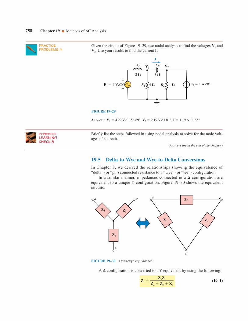
19.5 Delta-to-Wye and Wye-to-Delta ConversionsIn Chapter 8, we derived the relationships showing the equivalence of“delta” (or “pi”) connected resistance to a “wye” (or “tee”) configuration.
In a similar manner, impedances connected in a configuration areequivalent to a unique Y configuration. Figure 19–30 shows the equivalentcircuits.
758 Chapter 19 Methods of AC Analysis
PRACTICEPROBLEMS 4
Given the circuit of Figure 19–29, use nodal analysis to find the voltages V1 andV2. Use your results to find the current I.
XC
R1 R24
3
1 E1 4 V∠0
XL
2
I
V1 V2
I2 1 A∠0
FIGURE 19–29
Answers: V1 4.22 V∠56.89°, V2 2.19 V∠1.01°, I 1.19 A∠1.85°
Briefly list the steps followed in using nodal analysis to solve for the node volt-ages of a circuit.
(Answers are at the end of the chapter.)
IN-PROCESSLEARNINGCHECK 3
a
b
Z2
Z1 Z3
c Zb
ZaZc
a c
b
FIGURE 19–30 Delta-wye equivalence.
A configuration is converted to a Y equivalent by using the following:
Z1 Za
ZZbZ
b
c
Zc
(19–1)

Z2 Za
ZZaZ
b c
Zc
(19–2)
Z3 Za
ZZaZ
b
b
Zc
(19–3)
The above conversion indicates that the impedance in any arm of a Ycircuit is determined by taking the product of the two adjacent impedancesat this arm and dividing by the summation of the impedances.
If the impedances of the sides of the network are all equal (magnitudeand phase angle), the equivalent Y network will have identical impedances,where each impedance is determined as
ZY Z3
(19–4)
A Y configuration is converted to a equivalent by using the following:
Za (19–5)
Zb (19–6)
Zc (19–7)
Any impedance in a “” is determined by summing the possible two-impedance product combinations of the “Y” and then dividing by the imped-ance found in the opposite branch of the “Y.”
If the arms of a “Y” have identical impedances, the equivalent “” willhave impedances given as
Z 3ZY (19–8)
PRACTICE PROBLEMS 5
Z1Z2 Z1Z3 Z2Z3
Z3
Z1Z2 Z1Z3 Z2Z3
Z2
Z1Z2 Z1Z3 Z2Z3
Z1
Section 19.5 Delta-to-Wye and Wye-to-Delta Conversions 759
EXAMPLE 19–11 Determine the Y equivalent of the network shown inFigure 19–31.
Solution
Z1
3j
18j3
148.24∠2∠
4950°°
4.242 ∠135°
3.0 j3.0
(3 )(j6 )3 j6 j9
FIGURE 19–31
a
cb
3 6
9

760 Chapter 19 Methods of AC Analysis
Z2 3j2
7 j3
42.724
2∠∠
9405°°
6.364 ∠45°
4.5 j4.5
Z3 35
4 j3
45.2442∠
∠405°°
12.73 ∠45°
9.0 j9.0
In the above solution, we see that the given network has an equivalent Ynetwork with one arm having a negative resistance. This result indicates thatalthough the circuit has an equivalent Y circuit, the Y circuit cannot actu-ally be constructed from real components since negative resistors do not exist(although some active components may demonstrate negative resistance char-acteristics). If the given conversion is used to simplify a circuit we wouldtreat the impedance Z1 3 j3 as if the resistance actually were anegative value. Figure 19–32 shows the equivalent Y circuit.
( j9 )(j6 )3 j6 j9
(3 )( j9 )3 j6 j9
It is left to the student to show that the Y of Figure 19–32 is equivalent to the of Figure 19–31.
FIGURE 19–32
a
b c
3
j 3
9
j 9
j 4.5
4.5
EXAMPLE 19–12 Find the total impedance of the network in Figure 19–33.
FIGURE 19–33
3
3
6
a
cb 6
3
3
ZT

Section 19.5 Delta-to-Wye and Wye-to-Delta Conversions 761
Solution If we take a moment to examine this network, we see that the cir-cuit contains both a and a Y. In calculating the total impedance, the solutionis easier when we convert the Y to a .
The conversion is shown in Figure 19–34.
Za
j2
39 3
Zb
9
j3 j3
Zc 9
j3
j3
Now, substituting the equivalent into the original network, we have therevised network of Figure 19–35.
Z1Z2 Z1Z3 Z2Z3
Z3
Z1Z2 Z1Z3 Z2Z3
Z2
(3 )( j3 ) (3 )(j3 ) ( j3 )(j3 )
3
Z1Z2 Z1Z3 Z2Z3
Z1
3Ω
3Ω3Ω
Z2 Z3
Z1
Zc Zb
Za
a
b c b
a
c
FIGURE 19–34
3
3 3 3
6
6
a
cb
FIGURE 19–35
The network of Figure 19–35 shows that the corresponding sides of the areparallel. Because the inductor and the capacitor in the left side of the havethe same values, we may replace the parallel combination of these two com-ponents with an open circuit. The resulting impedance of the network is noweasily determined as
ZT 3 6 ( j3 )(j6 ) 2 j6
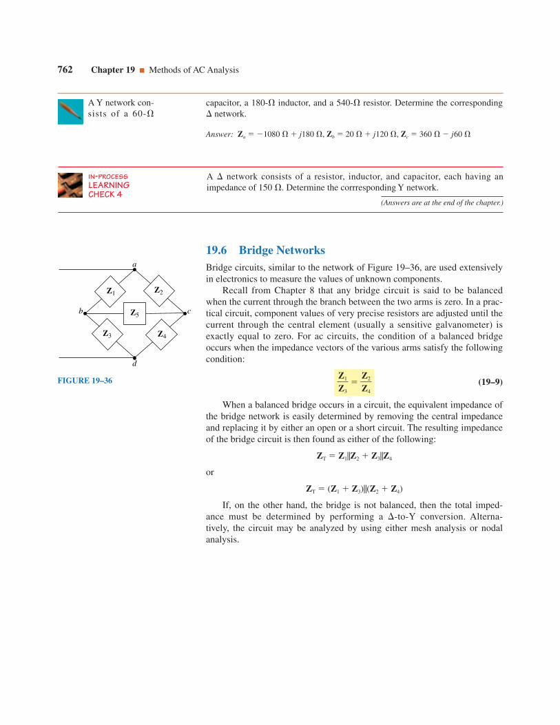
762 Chapter 19 Methods of AC Analysis
A Y network con-sists of a 60-
capacitor, a 180- inductor, and a 540- resistor. Determine the corresponding network.
Answer: Za 1080 j180 , Zb 20 j120 , Zc 360 j60
A network consists of a resistor, inductor, and capacitor, each having animpedance of 150 . Determine the corrresponding Y network.
(Answers are at the end of the chapter.)
IN-PROCESSLEARNINGCHECK 4
Z5
Z1
Z4
Z2
Z3
a
b c
d
FIGURE 19–36
19.6 Bridge NetworksBridge circuits, similar to the network of Figure 19–36, are used extensivelyin electronics to measure the values of unknown components.
Recall from Chapter 8 that any bridge circuit is said to be balancedwhen the current through the branch between the two arms is zero. In a prac-tical circuit, component values of very precise resistors are adjusted until thecurrent through the central element (usually a sensitive galvanometer) isexactly equal to zero. For ac circuits, the condition of a balanced bridgeoccurs when the impedance vectors of the various arms satisfy the followingcondition:
ZZ
1
3
ZZ
2
4
(19–9)
When a balanced bridge occurs in a circuit, the equivalent impedance ofthe bridge network is easily determined by removing the central impedanceand replacing it by either an open or a short circuit. The resulting impedanceof the bridge circuit is then found as either of the following:
ZT Z1Z2 Z3Z4
or
ZT (Z1 Z3)(Z2 Z4)
If, on the other hand, the bridge is not balanced, then the total imped-ance must be determined by performing a -to-Y conversion. Alterna-tively, the circuit may be analyzed by using either mesh analysis or nodalanalysis.

EXAMPLE 19–13 Given that the circuit of Figure 19–37 is a balancedbridge.
a. Calculate the unknown impedance, Zx.
b. Determine the values of Lx and Rx if the circuit operates at a frequency of1 kHz.
We will now consider various forms of bridge circuits which are used inelectronic circuits to determine the values of unknown inductors and capaci-tors. As in resistor bridges, the circuits use variable resistors together withvery sensitive galvanometer movements to ensure a balanced condition forthe bridge. However, rather than using a dc source to provide current in thecircuit, the bridge circuits use ac sources operating at a known frequency
Section 19.6 Bridge Networks 763
Z2
Zx
G
IG 0Z1
Z3
Z1 30 k∠20Z2 10 k∠0Z3 100 ∠0
Rx
Lx
Ef 1 kHz
FIGURE 19–37
Solutiona. The expression for the unknown impedance is determined from Equation
19–9 as
Zx ZZ2Z
1
3
(1
3
0
0
k
k
)
∠(1
00
20
°
)
33.3 ∠20°
31.3 j11.4
b. From the above result, we have
Rx 31.3
and
Lx 2
X
p
L
f
2p(
1
1
1
0
.
0
4
0
Hz) 1.81 mH

(usually 1 kHz). Once the bridge is balanced, the value of unknown induc-tance or capacitance may be easily determined by obtaining the readingdirectly from the instrument. Most instruments using bridge circuitry willincorporate several different bridges to enable the measurement of varioustypes of unknown impedances.
Maxwell BridgeThe Maxwell bridge, shown in Figure 19–38, is used to determine theinductance and series resistance of an inductor having a relatively largeseries resistance (in comparison to XL qL).
764 Chapter 19 Methods of AC Analysis
G
R1 R2
R3 RxLx
C
Z4
Z2
Z3
Z1IG 0
Eω
FIGURE 19–38 Maxwell bridge.
Resistors R1 and R3 are adjusted to provide the balanced condition (whenthe current through the galvanometer is zero: IG 0).
When the bridge is balanced, we know that the following condition mustapply:
ZZ
1
2
ZZ
3
4
If we write the impedances using the rectangular forms, we obtain
(R1)j q
1C
R1 j q
1C
Rx
R3
jqLx
R2
Rx
R
2R
jq3
Lx
q
C
jR
R1
1
j Rx
R
2R
jq3
Lx
(jR1)(Rx jqLx) R2R3(qCR1 j)
qLxR1 jR1Rx qR1R2R3C jR2R3
j q
R
C1
qR1
q
C
C
j1

Now, since two complex numbers can be equal only if their real partsare equal and if their imaginary parts are equal, we must have the follow-ing:
qLxR1 qR1R2R3C
and
R1Rx R2R3
Simplifying these expressions, we get the following equations for aMaxwell bridge:
Lx R2R3C (19–10)
and
Rx R
R2R
1
3 (19–11)
Section 19.6 Bridge Networks 765
EXAMPLE 19–14
a. Determine the values of R1 and R3 so that the bridge of Figure 19–39 isbalanced.
b. Calculate the current I when the bridge is balanced.
Solutiona. Rewriting Equations 19–10 and 19–11 and solving for the unknowns, we
have
R3 R
L
2Cx
(10 k
16
)(
m
0.
H
01 mF) 160
and
R1 R
R2R
x
3
(10 k
50
)(
160 ) 32 k
G
R110 k
R3
Lx
Rx
C 0.01F
IG 0
E 10 V∠0
R2
16 mH
50
I
f 1000 Hz
FIGURE 19–39

Schering BridgeThe Schering bridge, shown in Figure 19–41, is a circuit used to determinethe value of unknown capacitance.
By solving for the balanced bridge condition, we have the followingequations for the unknown quantities of the circuit:
Cx R
R1C
2
3 (19–14)
Hay BridgeIn order to measure the inductance and series resistance of an inductor hav-ing a small series resistance, a Hay bridge is generally used. The Hay bridgeis shown in Figure 19–40.
By applying a method similar to that used to determine the values of theunknown inductance and resistance of the Maxwell bridge, it may be shownthat the following equations for the Hay bridge apply:
Lx q2R
R
122
C
R32
C
1 (19–12)
and
Rx q
q2
2
R
R
1
12
R
C22
R
3C
1
2
(19–13)
766 Chapter 19 Methods of AC Analysis
G
R1 R2
R3 RxLx
C
Z4
Z2
Z3
Z1IG 0
Eω
G
R1 R2
C3
Rx
Cx
C1
Z4
Z2
Z3
Z1IG 0
Eω
FIGURE 19–40 Hay bridge. FIGURE 19–41 Schering bridge.
b. The total impedance is found as
ZT (ZCR1R2) [R3(Rx ZLx)]
ZT (j15.915 k)32 k10 k [160 (50 j100.5 )]
6.87 k∠25.6° 77.2 ∠38.0°
6.91 k∠25.0°
The resulting circuit current is
I 6.91
10k
V∠∠
0°25°
1.45 mA∠25.0°
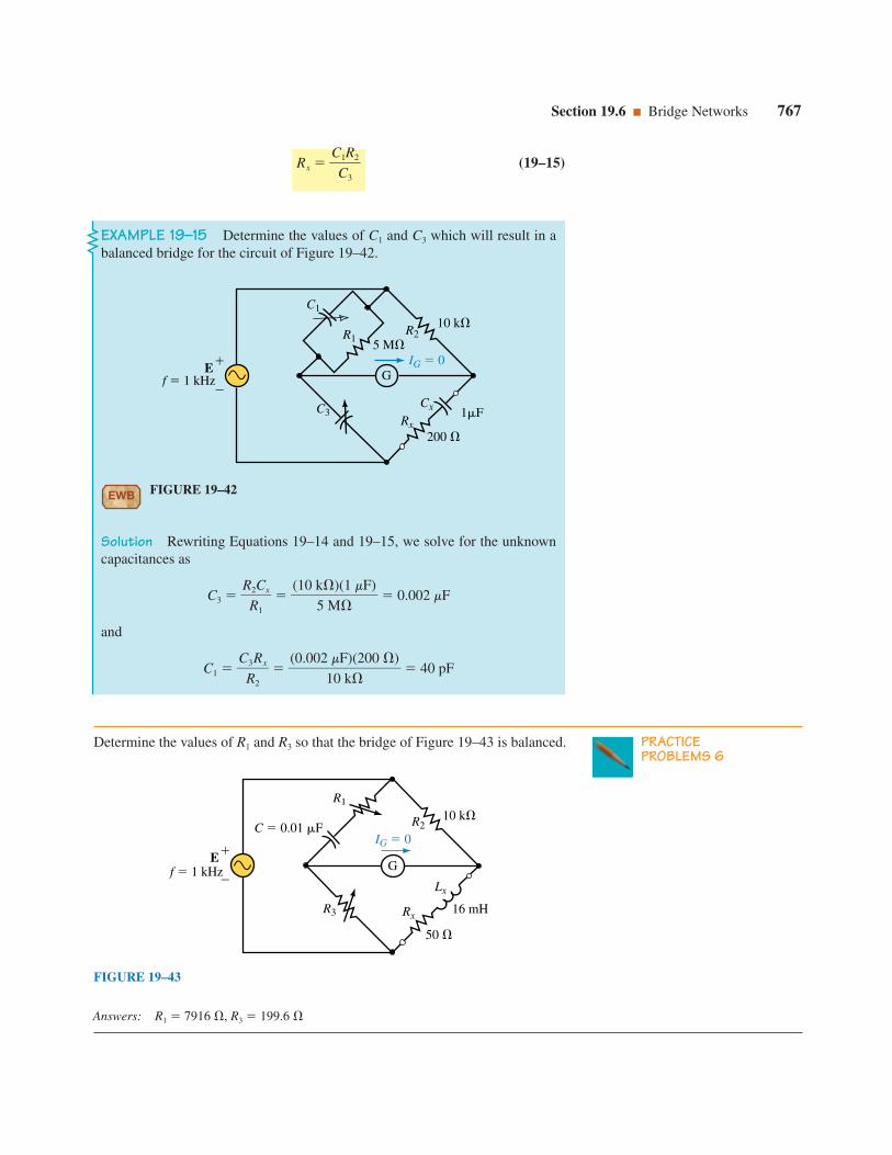
EXAMPLE 19–15 Determine the values of C1 and C3 which will result in abalanced bridge for the circuit of Figure 19–42.
G
R2
C3Rx
Cx
C1
IG 0E
f 1 kHz
5 M
200
10 k
1F
R1
EWB FIGURE 19–42
Answers: R1 7916 , R3 199.6
Section 19.6 Bridge Networks 767
Solution Rewriting Equations 19–14 and 19–15, we solve for the unknowncapacitances as
C3 R
R2C
1
x
(10 k
5
M
)(
1 mF) 0.002 mF
and
C1 C
R3R
2
x
(0.002
1
m
0
F
k
)
(200 ) 40 pF
PRACTICEPROBLEMS 6
Determine the values of R1 and R3 so that the bridge of Figure 19–43 is balanced.
G
R1
R2
R3 Rx
Lx
C 0.01 FIG 0
Ef 1 kHz
10 k
50
16 mH
FIGURE 19–43
Rx C
C1R
3
2 (19–15)

19.7 Circuit Analysis Using ComputersIn some of the examples in this chapter, we analyzed circuits that resultedin as many as three simultaneous linear equations. You have no doubt won-dered if there is a less complicated way to solve these circuits without theneed for using complex algebra. Computer programs are particularly usefulfor solving such ac circuits. Both Electronics Workbench and PSpice haveindividual strengths in the solution of ac circuits. As in previous examples,Electronics Workbench provides an excellent simulation of how measure-ments are taken in a lab. PSpice, on the other hand, provides voltage andcurrent readings, complete with magnitude and phase angle. The followingexamples show how these programs are useful for examining the circuits inthis chapter.
768 Chapter 19 Methods of AC Analysis
EXAMPLE 19–16 Use Electronics Workbench to show that the bridge cir-cuit of Figure 19–44 is balanced.
Solution Recall that a bridge circuit is balanced when the current throughthe branch between the two arms of the bridge is equal to zero. In this exam-ple, we will use a multimeter set on its ac ammeter range to verify the condi-tion of the circuit. The ammeter is selected by clicking on A and it is set to itsac range by clicking on the sinusoidal button. Figure 19–45 shows the circuitconnections and the ammeter reading. The results correspond to the condi-tions that were previously analyzed in Example 19–14. (Note: When usingElectronics Workbench, the ammeter may not show exactly zero current inthe balanced condition. This is due to the way the program does the calcula-tions. Any current less than 5 mA is considered to be effectively zero.)
G
10 k
160 k
32 k
0.01 F
E 10 V∠0
16 mH
50
f 1000 Hz
FIGURE 19–44
PSpiceELECTRONICSWORKBENCH

Section 19.7 Circuit Analysis Using Computers 769
EWB FIGURE 19–45
PRACTICEPROBLEMS 7
Use Electronics Workbench to verify that the results obtained in Example 19–15result in a balanced bridge circuit. (Assume that the bridge is balanced if the gal-vanometer current is less than 5 mA.)
OrCAD PSpice
EXAMPLE 19–17 Use OrCAD Capture CIS to input the circuit of Figure19–15. Assume that the circuit operates at a frequency of q 50 rad/s ( f 7.958 Hz). Use PSpice to obtain a printout showing the currents through XC,R2, and XL. Compare the results to those obtained in Example 19–6.
Solution Since the reactive components in Figure 19–15 were given asimpedance, it is necessary to first determine the corresponding values in hen-ries and farads.
L 50
4rad/s 80 mH
and
C (2 )(5
10 rad/s) 10 mF
Now we are ready to use OrCAD Capture to input the circuit as shown in Fig-ure 19–46. The basic steps are reviewed for you. Use the ac current source,

770 Chapter 19 Methods of AC Analysis
ISRC from the SOURCE library and place one IPRINT part from the SPE-CIAL library. The resistor, inductor, and capacitor are selected from theANALOG library and the ground symbol is selected by using the Placeground tool.
Change the value of the current source by double clicking on the part andmoving the horizontal scroll bar until you find the field titled AC. Type 1A40Deg into this field. A space must be placed between the magnitude andphase angle. Click on Apply. In order for these values to be displayed on theschematic, you must click on the Display button and then Value Only. Click onOK to return to the properties editor and then close the editor by clicking on X.
The IPRINT part is similar to an ammeter and provides a printout of thecurrent magnitude and phase angle. The properties of the IPRINT part arechanged by double clicking on the part and scrolling across to show theappropriate fields. Type OK in the AC, MAG, and PHASE fields. In order todisplay the selected fields on the schematic, you must click on the Displaybutton and then select Name and Value after changing each field. Since weneed to measure three currents in the circuit, we could follow this proceduretwo more times. However, an easier method is to click on the IPRINT partand copy the part by using CtrlC and CtrlV. Each IPRINTwill then have the same properties.
Once the rest of the circuit is completed and wired, click on the NewSimulation Profile tool. Give the simulation a name (such as ac Branch Cur-rents). Click on the Analysis tab and select AC Sweep/ Noise as the analysistype. Type the following values:
Start Frequency: 7.958Hz
End Frequency: 7.958Hz
Total Points: 1
FIGURE 19–46

PUTTING IT INTO PRACTICE
The Schering bridge of Figure 19–74 (p. 779) is balanced. In this chapter,you have learned several methods that allow you to find the current any-
where in a circuit. Using any method, determine the current through the gal-vanometer if the value of Cx 0.07 mF (All other values remain unchanged.)Repeat the calculations for a value of Cx 0.09 mF. Can you make a generalstatement for current through the galvanometer if Cx is smaller that the valuerequired to balance the bridge? What general statement can be made if thevalue of Cx is larger than the value in the balanced bridge?
19.1 Dependent Sources
1. Refer to the circuit of Figure 19–47.
Find V when the controlling current I is the following:
a. 20 mA∠0°
b. 50 mA∠180°
c. 60 mA∠60°
Problems 771
PRACTICEPROBLEMS 8
Use OrCAD PSpice to evaluate the node voltages for the circuit of Figure19–23. Assume that the circuit operates at an angular frequency of q 1000rad/s ( f 159.15 Hz).
PROBLEMS
Since we do not need the Probe postprocessor to run, it is disabled byselecting the Probe Window tab (from the Simulation Settings dialog box).Click on Display Probe window and exit the simulation settings by clickingon OK.
Click on the Run tool. Once PSpice has successfully run, click on theView menu and select the Output File menu item. Scroll through the file untilthe currents are shown as follows:
FREQ IM(V_PRINT1)IP(V_PRINT1)
7.958E+00 7.887E-01 -1.201E+02
FREQ IM(V_PRINT2)IP(V_PRINT2)
7.958E+00 1.304E+00 1.560E+02
FREQ IM(V_PRINT3)IP(V_PRINT3)
7.958E+00 1.450E+00 -5.673E+01
The above printout provides: I1 0.7887 A∠120.1°, I2 1.304 A∠156.0°,and I3 1.450 A∠56.73°. These results are consistent with those calcu-lated in Example 19–6.

772 Chapter 19 Methods of AC Analysis
(800 )I
40 k
10 k VI R 1 k
200 V
100 k
20 k
IR 2 k
V
FIGURE 19–48
FIGURE 19–49
I
(6.0 mS)V 30 k60 kR 2 k
V
FIGURE 19–50
I 60 IR 1 k
5 k V25 k
FIGURE 19–47
2. Refer to the circuit of Figure 19–48.
Find I when the controlling voltage, V, is the following:
a. 30 mV∠0°
b. 60 mV∠180°
c. 100 mV∠30°
3. Repeat Problem 1 for the circuit of Figure 19–49.
4. Repeat Problem 2 for the circuit of Figure 19–50.

6. Repeat Problem 5 for the circuit of Figure 19–52.
Problems 773
I
130 I 20 k30 k
R2 R32 k
10 mV∠30Vout
R1
FIGURE 19–51
5 k20 k
R2 R31.5 k
20 mV∠0Vout
R1
V1
(5 mS) V1
XC
2 k
FIGURE 19–52
5. Find the output voltage, Vout, for the circuit of Figure 19–51.
600 1800
RL30 mA∠0 VL
(a) (b)
1 k225
RL2 mA∠30 VL
FIGURE 19–53
(a)
40
5 V∠25
(b)
40
82 V∠70
9
FIGURE 19–54
19.2 Source Conversion
7. Given the circuits of Figure 19–53, convert each of the current sources intoan equivalent voltage source. Use the resulting circuit to find VL.
8. Convert each voltage source of Figure 19–54 into an equivalent currentsource.
9. Refer to the circuit of Figure 19–55.
a. Solve for the voltage, V.

b. Convert the current source into an equivalent voltage source and againsolve for V. Compare to the result obtained in (a).
774 Chapter 19 Methods of AC Analysis
12
4 8
2
3
5
I
20 V∠0 30 V∠30
12
5
I
2 V∠40
4 V∠2030
25
16
FIGURE 19–57 FIGURE 19–58
19.3 Mesh (Loop) Analysis
11. Consider the circuit of Figure 19–57.
a. Write the mesh equations for the circuit.
b. Solve for the loop currents.
c. Determine the current I through the 4- resistor.
10 k50 k
V150 I2 k30 mV∠0
6 k
I
FIGURE 19–55
40 k120 k
VL
(5 mS)V10 k
I 3 A∠0
RL
V
FIGURE 19–56
10. Refer to the circuit of Figure 19–56.
a. Solve for the voltage, VL.
b. Convert the current source into an equivalent voltage source and againsolve for VL.
c. If I 5 mA∠90°, what is VL?
12. Refer to the circuit of Figure 19–58.
a. Write the mesh equations for the circuit.
b. Solve for the loop currents.
c. Determine the current through the 25- inductor.

Problems 775
10
V
25
2 A∠0
9
15 12
10 V∠0 15 V∠6010
FIGURE 19–59
13. Refer to the circuit of Figure 19–59.
a. Simplify the circuit and write the mesh equations.
b. Solve for the loop currents.
c. Determine the voltage V across the 15- capacitor.
V
3
3 V∠90
2
4
2 4 A∠0
2 A∠45
I
FIGURE 19–60
V
18 V∠0
3 k
I
30 V∠53.13
4 k
8 k
XL
R2
5 mA∠30
XC
4 k
R1
FIGURE 19–61
14. Consider the circuit of Figure 19–60.
a. Simplify the circuit and write the mesh equations.
b. Solve for the loop currents.
c. Determine the voltage V across the 2- resistor.
15. Use mesh analysis to find the current I and the voltage V in the circuit ofFigure 19–61.

16. Repeat Problem 15 for the circuit of Figure 19–62.
776 Chapter 19 Methods of AC Analysis
2 A∠0 6 I
4
3 A∠90
4 A∠90
3
V
3
2 A∠90
3 A∠90
2
6
2 A∠0
FIGURE 19–63 FIGURE 19–64
18. Refer to the circuit of Figure 19–64.
a. Write the nodal equations.
b. Solve for the node voltages.
c. Determine the voltage V across the 3- capacitor.
19. a. Simplify the circuit of Figure 19–59, and write the nodal equations.
b. Solve for the node voltages.
c. Determine the voltage across the 15- capacitor.
20. a. Simplify the circuit of Figure 19–60, and write the nodal equations.
b.Solve for the node voltages.
c. Determine the current through the 2- resistor.
21. Use nodal analysis to determine the node voltages in the circuit of Figure19–61. Use the results to find the current I and the voltage V. Compare youranswers to those obtained using mesh analysis in Problem 15.
22. Use nodal analysis to determine the node voltages in the circuit of Figure19–62. Use the results to find the current I and the voltage V. Compare youranswers to those obtained using mesh analysis in Problem 16.
V
30 V∠30
9 k
10 k12 k
16 k
1 mA∠0
R1
XC1
XC2
XL
R2 4 k R3 3 k
I
FIGURE 19–62
19.4 Nodal Analysis
17. Consider the circuit of Figure 19–63.
a. Write the nodal equations.
b. Solve for the node voltages.
c. Determine the current I through the 4- capacitor.

19.5 Delta-to-Wye and Wye-to-Delta Conversions
23. Convert each of the networks of Figure 19–65 into an equivalent Y net-work.
24. Convert each of the Y networks of Figure 19–66 into an equivalent net-work.
Problems 777
(a)
270
a
b c
90
810
(b)
18 k36 k
9 k
a
b c
FIGURE 19–65
25
50 75
(a)
(b)
2 k
2 k3 k
FIGURE 19–66
I
10 V∠0
2
5
6
15 10 18
3
25 V∠30
I
10
3
3
10
10
FIGURE 19–67 FIGURE 19–68
I
16 V∠0 ZT3 k
6 k
6 k
3 k
2 k
9 k
I1
FIGURE 19–69
25. Using →Y or Y→ conversion, calculate I for the circuit of Figure 19–67.
26. Using →Y or Y→ conversion, calculate I for the circuit of Figure 19–68.
27. Refer to the circuit of Figure 19–69:
a. Determine the equivalent impedance, ZT, of the circuit.
b. Find the currents I and I1.

28. Refer to the circuit of Figure 19–70:
a. Determine the equivalent impedance, ZT, of the circuit.
b. Find the voltages V and V1.
778 Chapter 19 Methods of AC Analysis
500 mV∠0
1
2
3
4
2
G
IG 0
IZ2
FIGURE 19–71
G
IG 0
20 V∠0
I
25 k
50 k
200
5 kZ1
FIGURE 19–72
19.6 Bridge Networks
29. Given that the bridge circuit of Figure 19–71 is balanced:
a. Determine the value of the unknown impedance.
b. Solve for the current I.
30. Given that the bridge circuit of Figure 19–72 is balanced:
a. Determine the value of the unknown impedance.
b. Solve for the current I.
31. Show that the bridge circuit of Figure 19–73 is balanced.
32. Show that the bridge circuit of Figure 19–74 is balanced.
33. Derive Equations 19–14 and 19–15 for the balanced Schering bridge.
34. Derive Equations 19–12 and 19–13 for the balanced Hay bridge.
10 mA∠0 10 k
2 k
8 k
5 H
0.2 F
0.1 FV1
V 1 krad/s
FIGURE 19–70
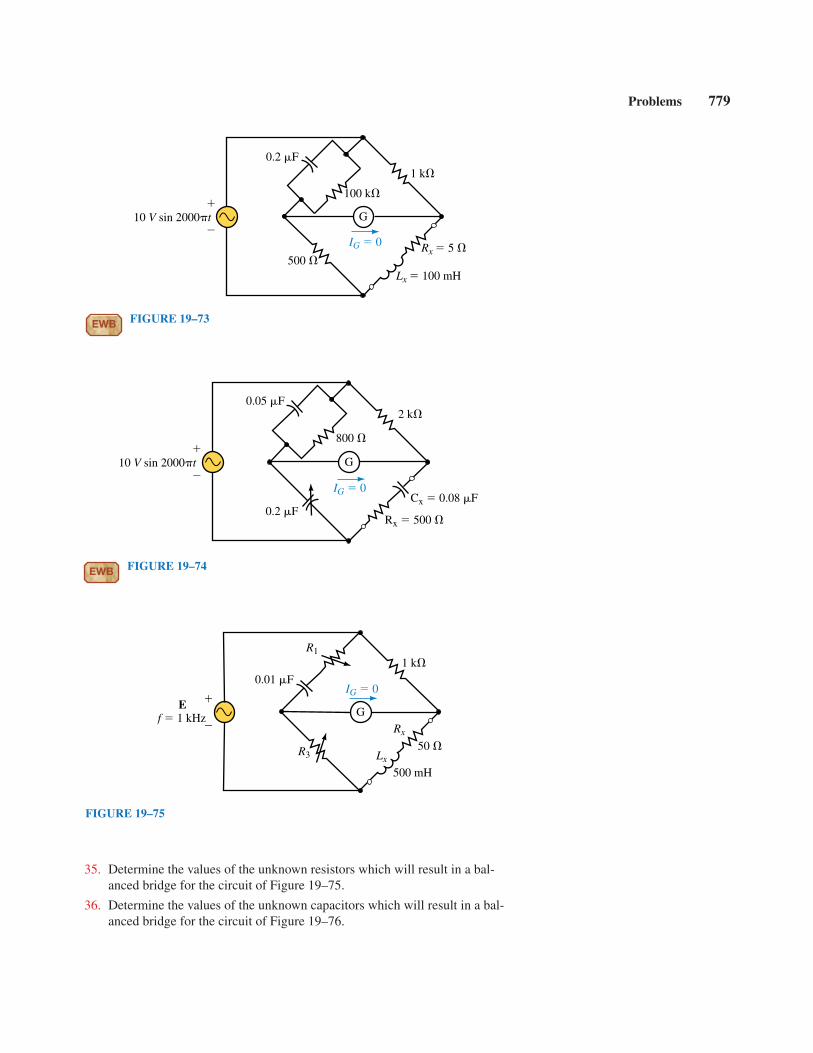
Problems 779
G
100 k
1 k
Rx 5 IG 0
10 V sin 2000t
500 Lx 100 mH
0.2 F
EWB FIGURE 19–73
G
IG 0
800
Rx 500
2 k
Cx 0.08 F
10 V sin 2000t
0.2 F
0.05 F
EWB FIGURE 19–74
35. Determine the values of the unknown resistors which will result in a bal-anced bridge for the circuit of Figure 19–75.
36. Determine the values of the unknown capacitors which will result in a bal-anced bridge for the circuit of Figure 19–76.
G
R1
R3
Rx
Lx
IG 0E
1 k
50
500 mH
0.01 F
f 1 kHz
FIGURE 19–75

19.7 Circuit Analysis Using Computers
37. EWB Use Electronics Workbench to show that the bridge circuit of Figure19–73 is balanced. (Assume that the bridge is balanced if the galvanometercurrent is less than 5 mA.)
38. EWB Repeat Problem 37 for the bridge circuit of Figure 19–74.
39. PSpice Use the OrCAD Capture to input the file for the circuit of Figure19–21. Assume that the circuit operates at a frequency q 2 krad/s. UseIPRINT and VPRINT to obtain a printout of the node voltages and the cur-rent through each element of the circuit.
40. PSpice Use the OrCAD Capture to input the file for the circuit of Figure19–29. Assume that the circuit operates at a frequency q 1 krad/s. UseIPRINT and VPRINT to obtain a printout of the node voltages and the cur-rent through each element of the circuit.
41. PSpice Use the OrCAD Capture to input the file for the circuit of Figure19–68. Assume that the circuit operates at a frequency q 20 rad/s. UseIPRINT to obtain a printout of the current I.
42. PSpice Use the OrCAD Capture to input the file for the circuit of Figure19–69. Assume that the circuit operates at a frequency q 3 krad/s. UseIPRINT to obtain a printout of the current I.
780 Chapter 19 Methods of AC Analysis
ANSWERS TO IN-PROCESSLEARNING CHECKS
In-Process Learning Check 1
a. E 1000 V∠30°
b. E 4 V∠90°
c. E 1024 V∠38.66°
In-Process Learning Check 2
1. Convert current sources to voltage sources.
2. Redraw the circuit.
3. Assign a clockwise current to each loop.
4. Write loop equations using Kirchhoff’s voltage law.
5. Solve the resulting simultaneous linear equations to find the loop currents.
G
C3 Rx
Cx
C1
IG 0
E
1 M
5 k
1 k
0.1 F
f 1 kHz
FIGURE 19–76

In-Process Learning Check 3
1. Convert voltage sources to current sources.
2. Redraw the circuit.
3. Label all nodes, including the reference node.
4. Write nodal equations using Kirchhoff’s current law.
5. Solve the resulting simultaneous linear equations to find the node voltages.
In-Process Learning Check 4Z1 150 ∠90° Z2 150 ∠90° Z3 150 ∠0°
Answers to In-Process Learning Checks 781
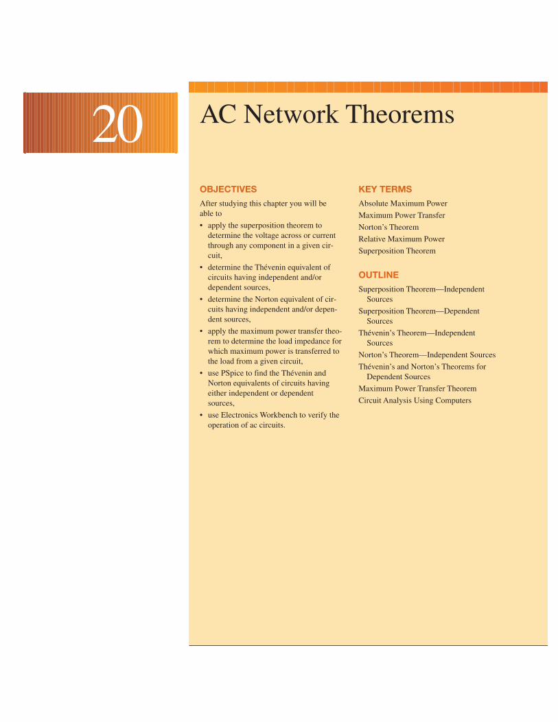
OBJECTIVES
After studying this chapter you will beable to
• apply the superposition theorem todetermine the voltage across or currentthrough any component in a given cir-cuit,
• determine the Thévenin equivalent ofcircuits having independent and/ordependent sources,
• determine the Norton equivalent of cir-cuits having independent and/or depen-dent sources,
• apply the maximum power transfer theo-rem to determine the load impedance forwhich maximum power is transferred tothe load from a given circuit,
• use PSpice to find the Thévenin andNorton equivalents of circuits havingeither independent or dependentsources,
• use Electronics Workbench to verify theoperation of ac circuits.
KEY TERMS
Absolute Maximum Power
Maximum Power Transfer
Norton’s Theorem
Relative Maximum Power
Superposition Theorem
OUTLINE
Superposition Theorem—IndependentSources
Superposition Theorem—DependentSources
Thévenin’s Theorem—IndependentSources
Norton’s Theorem—Independent Sources
Thévenin’s and Norton’s Theorems forDependent Sources
Maximum Power Transfer Theorem
Circuit Analysis Using Computers
AC Network Theorems20

In this chapter we apply the superposition, Thévenin, Norton, and maximumpower transfer theorems in the analysis of ac circuits. Although the Millman
and reciprocity theorems apply to ac circuits as well as to dc circuits, they areomitted since the applications are virtually identical with those used in analyzingdc circuits.
Many of the techniques used in this chapter are similar to those used inChapter 9, and as a result, most students will find a brief review of dc theoremsuseful.
This chapter examines the application of the network theorems by consider-ing both independent and dependent sources. In order to show the distinctionsbetween the methods used in analyzing the various types of sources, the sectionsare labelled according to the types of sources involved.
An understanding of dependent sources is particularly useful when workingwith transistor circuits and operational amplifiers. Sections 20.2 and 20.5 areintended to provide the background for analyzing the operation of feedbackamplifiers. Your instructor may find that these topics are best left until you coverthis topic in a course dealing with such amplifiers. Consequently, the omissionof sections 20.2 and 20.5 will not in any way detract from the continuity of theimportant ideas presented in this chapter.
783
CHAPTER PREVIEW
PUTTING IT INPERSPECTIVE
William Bradford Shockley
SHOCKLEY WAS BORN the son of a mining engineer in London, England on Feb-ruary 13, 1910. After graduating from the California Institute of Technology andMassachusetts Institute of Technology, Shockley joined Bell Telephone Labora-tories.
With his co-workers, John Bardeen and Walter Brattain, Shockley devel-oped an improved solid-state rectifier using a germanium crystal which had beeninjected with minute amounts of impurities. Unlike vacuum tubes, the resultingdiodes were able to operate at much lower voltages without the need for ineffi-cient heater elements.
In 1948, Shockley combined three layers of germanium to produce a devicewhich was able to not only rectify a signal but to amplify it. Thus was developedthe first transistor. Since its humble beginning, the transistor has been improvedand decreased in size to the point where now a circuit containing thousands oftransistors can easily fit into an area not much bigger than the head of a pin.
The advent of the transistor has permitted the construction of elaboratespacecraft, unprecedented communication, and new forms of energy generation.
Shockley, Bardeen, and Brattain received the 1956 Nobel Prize in Physicsfor their discovery of the transistor.

20.1 Superposition Theorem—Independent SourcesThe superposition theorem states the following:
The voltage across (or current through) an element is determined by sum-ming the voltage (or current) due to each independent source.
In order to apply this theorem, all sources other than the one being consid-ered are eliminated. As in dc circuits, this is done by replacing current sourceswith open circuits and by replacing voltage sources with short circuits. Theprocess is repeated until the effects due to all sources have been determined.
Although we generally work with circuits having all sources at the samefrequency, occasionally a circuit may operate at more than one frequency ata time. This is particularly true in diode and transistor circuits which use a dcsource to set a “bias” (or operating) point and an ac source to provide thesignal to be conditioned or amplified. In such cases, the resulting voltages orcurrents are still determined by applying the superposition theorem. Thetopic of how to solve circuits operating at several different frequenciessimultaneously is covered in Chapter 25.
784 Chapter 20 AC Network Theorems
As in dc circuits, the superposi-tion theorem can be applied onlyto voltage and current; it cannotbe used to solve for the totalpower dissipated by an element.This is because power is not alinear quantity, but rather fol-lows a square-law relationship(P V2/R I2R).
NOTES...
EXAMPLE 20–1 Determine the current I in Figure 20–1 by using thesuperposition theorem.
SolutionCurrent due to the 5 V∠0° voltage source: Eliminating the current source,we obtain the circuit shown in Figure 20–2.
2 5 V∠0
2 A∠0
4 5
I
FIGURE 20–1
Current source isreplaced with an open
circuit.
2
5 V∠0
4 5
I(1)
FIGURE 20–2

Section 20.1 Superposition Theorem—Independent Sources 785
Applying Ohm’s law, we have
I(1) 45
V∠j2
0°
4.472
5
V∠
∠
02°6.57°
1.118 A∠26.57°
Current due to the 2 A∠0° current source: Eliminating the voltage source,we obtain the circuit shown in Figure 20–3.
The current I(2) due to this source is determined by applying the currentdivider rule:
I(2) (2 A∠0°) 4
4
∠j02°
4.472
8V∠∠
02°6.57°
1.789 A∠26.57°
The total current is determined as the summation of currents I(1) and I(2):
I I(1) I(2)
1.118 A∠26.57° 1.789 A∠26.57°
(1.0 A j0.5 A) (1.6 A j0.8 A)
2.6 j1.3 A
2.91 A∠26.57°
2
2 A∠0
4 5
I(2)
Voltage source isreplaced with a
short circuit.
FIGURE 20–3
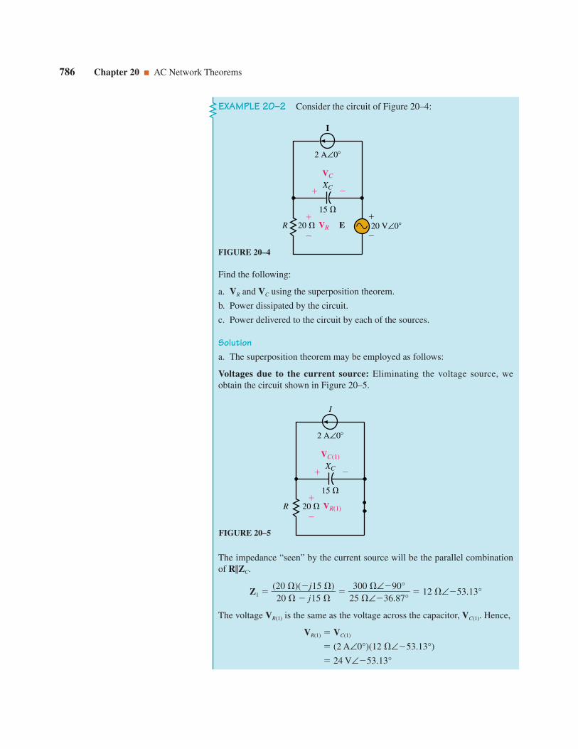
786 Chapter 20 AC Network Theorems
EXAMPLE 20–2 Consider the circuit of Figure 20–4:
Find the following:
a. VR and VC using the superposition theorem.
b. Power dissipated by the circuit.
c. Power delivered to the circuit by each of the sources.
Solutiona. The superposition theorem may be employed as follows:
Voltages due to the current source: Eliminating the voltage source, weobtain the circuit shown in Figure 20–5.
FIGURE 20–4
2 A∠0
15
20 R
I
E 20 V∠0
VC
VR
XC
The impedance “seen” by the current source will be the parallel combinationof RZC.
Z1 (2200
)(
jj1155
)
23500
∠
∠3
69.807°°
12 ∠53.13°
The voltage VR(1) is the same as the voltage across the capacitor, VC(1). Hence,
VR(1) VC(1)
(2 A∠0°)(12 ∠53.13°)
24 V∠53.13°
FIGURE 20–5
2 A∠0
15
20 R
I
VC(1)
VR(1)
XC

Section 20.1 Superposition Theorem—Independent Sources 787
Voltages due to the voltage source: Eliminating the current source, wehave the circuit shown in Figure 20–6.
The voltages VR(2) and VC(2) are determined by applying the voltage divider rule,
VR(2) 20
20
∠j105°
(20 V∠0°)
25
40∠0
V3∠6.
08°7°
16 V∠36.87°
and
VC(2)
2015
∠j
1590°
(20 V∠0°)
2350∠0
V3∠69.807°°
12 V∠126.87°
Notice that VC(2) is assigned to be negative relative to the originally assumedpolarity. The negative sign is eliminated from the calculation by adding (orsubtracting) 180° from the corresponding calculation.
By applying superposition, we get
VR VR(1) VR(2)
24 V∠53.13° 16 V∠36.87°
(14.4 V j19.2 V) (12.8 V j9.6 V)
27.2 V j9.6 V
28.84 V∠19.44°
and
VC VC(1) VC(2)
24 V∠53.13° 12 V∠126.87°
(14.4 V j19.2 V) (7.2 V j9.6 V)
7.2 V j9.6 V
12 V∠53.13°
b. Since only the resistor will dissipate power, the total power dissipated bythe circuit is found as
PT (28
2.084
V)2
41.60 W
FIGURE 20–6
15
20 R 20 V∠0
VC(2)
VR(2)
XC
E

788 Chapter 20 AC Network Theorems
c. The power delivered to the circuit by the current source is
P1 V1I cos v1
where V1 VC 12 V∠53.13° is the voltage across the current source andv1 is the phase angle between V1 and I.
The power delivered by the current source is
P1 (12 V)(2 A) cos 53.13° 14.4 W
The power delivered to the circuit by the voltage source is similarly deter-mined as
P2 EI2 cos v2
where I2 is the current through the voltage source and v2 is the phase anglebetween E and I2.
P2 (20 V)282.084
V
cos 19.44° 27.2 W
As expected, the total power delivered to the circuit must be the summation
PT P1 P2 41.6 W
PRACTICEPROBLEMS 1
Use superposition to find V and I for the circuit of Figure 20–7.
FIGURE 20–7
3 5 V∠302 A∠0
4
I
V
Answers: I 2.52 A∠25.41°, V 4.45 V∠104.18°
A 20- resistor is in a circuit having three sinusoidal sources. After analyzingthe circuit, it is found that the current through the resistor due to each of thesources is as follows:
I1 1.5 A∠20°
I2 1.0 A∠110°
I3 2.0 A∠0°
a. Use superposition to calculate the resultant current through the resistor.
b. Calculate the power dissipated by the resistor.
c. Show that the power dissipated by the resistor cannot be found by applyingsuperposition, namely, PT I2
1R I22R I2
3R.
(Answers are at the end of the chapter.)
IN-PROCESSLEARNINGCHECK 1

20.2 Superposition Theorem—Dependent SourcesChapter 19 introduced the concept of dependent sources. We now examineac circuits which are powered by dependent sources. In order to analyze cir-cuits having dependent sources, it is first necessary to determine whether thedependent source is conditional upon a controlling element in its own circuitor whether the controlling element is located in some other circuit.
If the controlling element is external to the circuit under consideration,the method of analysis is the same as for an independent source. However, ifthe controlling element is in the same circuit, the analysis follows a slightlydifferent stategy. The next two examples show the techniques used to ana-lyze circuits having dependent sources.
Section 20.2 Superposition Theorem—Dependent Sources 789
EXAMPLE 20–3 Consider the circuit of Figure 20–8.
a. Determine the general expression for V in terms of I.
b. Calculate V if I 1.0 A∠0°.
c. Calculate V if I 0.3 A∠90°.
Solutiona. Since the current source in the circuit is dependent on current through an
element which is located outside of the circuit of interest, the circuit maybe analyzed in the same manner as for independent sources.
Voltage due to the voltage source: Eliminating the current source, we obtainthe circuit shown in Figure 20–9.
2 6 V∠05 I
R2
V
R1
8 I
R
FIGURE 20–8
FIGURE 20–9
2 6 V∠0
R2
V(1)
R1
8
V(1) 180 (6 V∠0°) 4.8 V∠0°
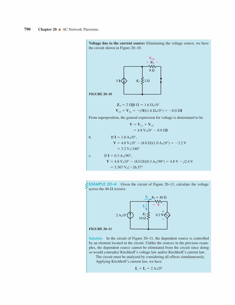
790 Chapter 20 AC Network Theorems
Voltage due to the current source: Eliminating the voltage source, we havethe circuit shown in Figure 20–10.
ZT 2 8 1.6 ∠0°
V(2) VZT (5I)(1.6 ∠0°) 8.0 I
From superposition, the general expression for voltage is determined to be
V V(1) V(2)
4.8 V∠0° 8.0 I
b. If I 1.0 A∠0°,
V 4.8 V∠0° (8.0 )(1.0 A∠0°) 3.2 V
3.2 V∠180°
c. If I 0.3 A∠90°,
V 4.8 V∠0° (8.0 )(0.3 A∠90°) 4.8 V j2.4 V
5.367 V∠26.57°
FIGURE 20–10
2 5 I
R2 V(2)
R1
8
EXAMPLE 20–4 Given the circuit of Figure 20–11, calculate the voltageacross the 40- resistor.
Solution In the circuit of Figure 20–11, the dependent source is controlledby an element located in the circuit. Unlike the sources in the previous exam-ples, the dependent source cannot be eliminated from the circuit since doingso would contradict Kirchhoff’s voltage law and/or Kirchhoff’s current law.
The circuit must be analyzed by considering all effects simultaneously.Applying Kirchhoff’s current law, we have
I1 I2 2 A∠0°
FIGURE 20–11
10 0.2 V2 A∠0
I1 V
R1
I2 R2 40

20.3 Thévenin’s Theorem—Independent SourcesThévenin’s theorem is a method which converts any linear bilateral ac circuitinto a single ac voltage source in series with an equivalent impedance asshown in Figure 20–13.
The resulting two-terminal network will be equivalent when it is con-nected to any external branch or component. If the original circuit containsreactive elements, the Thévenin equivalent circuit will be valid only at thefrequency at which the reactances were determined. The following methodmay be used to determine the Thévenin equivalent of an ac circuit havingeither independent sources or sources which are dependent upon voltage orcurrent in some other circuit. The outlined method may not be used in cir-cuits having dependent sources controlled by voltage or current in the samecircuit.
1. Remove the branch across which the Thévenin equivalent circuit is to befound. Label the resulting two terminals. Although any designation willdo, we will use the notations a and b.
2. Set all sources to zero. As in dc circuits, this is achieved by replacingvoltage sources with short circuits and current sources with open circuits.
Section 20.3 Thévenin’s Theorem—Independent Sources 791
From Kirchhoff’s voltage law, we have
(10 ) I1 V 0.2 V 1.2 V
I1 0.12 V
and,
I2 40
V 0.025 V
Combining the above expressions, we have
0.12 V 0.025 V 2.0 A∠0°
0.145 V 2.0 A∠0°
V 13.79 V∠0°
PRACTICEPROBLEMS 2
Determine the voltage V in the circuit of Figure 20–12.
10
5 A∠0
I
V2 2 I
3
FIGURE 20–12
Answer: V 2.73 V∠180°
ETh
a
b
ZTh
FIGURE 20–13 Thévenin equivalentcircuit.

3. Determine the Thévenin equivalent impedance, ZTh by calculating theimpedance seen between the open terminals a and b. Occasionally it maybe necessary to redraw the circuit to simplify this process.
4. Replace the sources removed in Step 3 and determine the open-circuit volt-age across the terminals a and b. If any of the sources are expressed in sinu-soidal form, it is first necessary to convert these sources into an equivalentphasor form. For circuits having more than one source, it may be necessaryto apply the superposition theorem to calculate the open-circuit voltage.Since all voltages will be phasors, the resultant is found by using vectoralgebra. The open-circuit voltage is the Thévenin voltage, ETh.
5. Sketch the resulting Thévenin equivalent circuit by including that portionof the circuit removed in Step 1.
792 Chapter 20 AC Network Theorems
EXAMPLE 20–5 Find the Thévenin equivalent circuit external to ZL forthe circuit of Figure 20–14.
SolutionSteps 1 and 2: Removing the load impedance ZL and setting the voltagesource to zero, we have the circuit of Figure 20–15.
60
20 V∠0
80
40
XC
XL
R ZL
a
b
FIGURE 20–14
60
80
40
XC
XL
R ZTh
Voltage source isreplaced with a
short circuit.
a
b
FIGURE 20–15

Section 20.3 Thévenin’s Theorem—Independent Sources 793
Step 3: The Thévenin impedance between terminals a and b is found as
ZTh R(ZL ZC)
44
8.7020
∠∠
2960.°57°
17.89 ∠63.43°
8 j16
Step 4: The Thévenin voltage is found by using the voltage divider rule asshown in the circuit of Figure 20–16.
(40 ∠0°)(20 ∠90°)
40 j20
ETh Vab (20 V∠0°)
44.7
8200
V∠∠206°.57°
17.89 V∠26.57°
Step 5: The resultant Thévenin equivalent circuit is shown in Figure 20–17.
40 ∠0°40 j80 j60
FIGURE 20–16 60
20 V∠0
80
40
XC
XL
R
a
b
17.89 V∠26.6
8 j16
ZLETh
ZTha
b
FIGURE 20–17
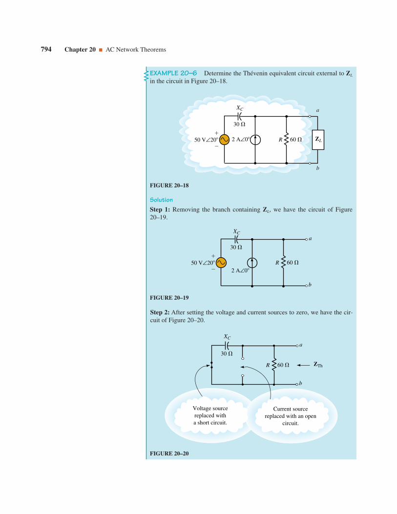
794 Chapter 20 AC Network Theorems
EXAMPLE 20–6 Determine the Thévenin equivalent circuit external to ZL
in the circuit in Figure 20–18.
SolutionStep 1: Removing the branch containing ZL, we have the circuit of Figure20–19.
50 V∠20
30
60
XC
R ZL2 A∠0
a
b
FIGURE 20–18
Step 2: After setting the voltage and current sources to zero, we have the cir-cuit of Figure 20–20.
50 V∠202 A∠0
30
60
XC
R
a
b
FIGURE 20–19
30
60
XC
R
a
b
ZTh
Current sourcereplaced with an open
circuit.
Voltage sourcereplaced witha short circuit.
FIGURE 20–20
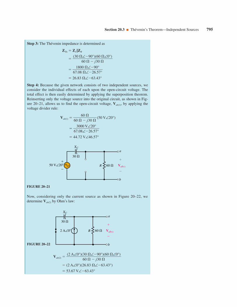
Section 20.3 Thévenin’s Theorem—Independent Sources 795
Step 3: The Thévenin impedance is determined as
ZTh ZCZR
67
1.80080∠∠
2960.5°7°
26.83 ∠63.43°
Step 4: Because the given network consists of two independent sources, weconsider the individual effects of each upon the open-circuit voltage. Thetotal effect is then easily determined by applying the superposition theorem.Reinserting only the voltage source into the original circuit, as shown in Fig-ure 20–21, allows us to find the open-circuit voltage, Vab(1), by applying thevoltage divider rule:
Vab(1) 60
6
0 j30 (50 V∠20°)
67
3.00080∠
V
∠26
2.05°7°
44.72 V∠46.57°
(30 ∠90°)(60 ∠0°)
60 j30
Now, considering only the current source as shown in Figure 20–22, wedetermine Vab(2) by Ohm’s law:
30
60
XC
R
a
b
50 V∠20 Vab(1)
FIGURE 20–21
2 A∠0
30
60
XC
R
a
b
Vab(2)
FIGURE 20–22
Vab(2)
(2 A∠0°)(26.83 ∠63.43°)
53.67 V∠63.43°
(2 A∠0°)(30 ∠90°)(60 ∠0°)
60 j30

796 Chapter 20 AC Network Theorems
From the superposition theorem, the Thévenin voltage is determined as
ETh Vab(1) Vab(2)
44.72 V∠46.57° 53.67 V∠63.43°
(30.74 V j32.48 V) (24.00 V j48.00 V)
(54.74 V j15.52 V) 56.90 V∠15.83°
Step 5: The resulting Thévenin equivalent circuit is shown in Figure 20–23.
56.9 V∠15.8
26.8 ∠ 63.43
ZL
ETh
a
b
ZTh
FIGURE 20–23
Refer to the circuit shown in Figure 20–24 of Practice Problem 3. List the stepsthat you would use to find the Thévenin equivalent circuit.
(Answers are at the end of the chapter.)
IN-PROCESSLEARNINGCHECK 2
PRACTICEPROBLEMS 3
a. Find the Thévenin equivalent circuit external to the inductor in the circuit inFigure 20–24. (Notice that the voltage source is shown as sinusoidal.)
b. Use the Thévenin equivalent circuit to find the phasor output voltage, VL.
c. Convert the answer of (b) into the equivalent sinusoidal voltage.
Answers:a. ZTh 1.5 k j2.0 k 2.5 k∠53.13°, ETh 3.16 V∠63.43°
b. VL 1.75 V∠60.26°
c. vL 2.48 sin(2000t 60.26°)
0.2 F10 sin 2000t
R1 5 k
C
500 mHL VL
R2 0.5 k a
b
FIGURE 20–24

20.4 Norton’s Theorem—Independent SourcesNorton’s theorem converts any linear bilateral network into an equivalentcircuit consisting of a single current source and a parallel impedance asshown in Figure 20–25.
Although Norton’s equivalent circuit may be determined by first findingthe Thévenin equivalent circuit and then performing a source conversion, wegenerally use the more direct method outlined below. The steps to find theNorton equivalent cirucuit are as follows:
1. Remove the branch across which the Norton equivalent circuit is to befound. Label the resulting two terminals a and b.
2. Set all sources to zero.
3. Determine the Norton equivalent impedance, ZN, by calculating the imped-ance seen between the open terminals a and b.
NOTE: Since the previous steps are identical with those followed for find-ing the Thévenin equivalent circuit, we conclude that the Norton imped-ance must be the same as the Thévenin impedance.
4. Replace the sources removed in Step 3 and determine the current thatwould occur between terminals a and b if these terminals were shorted.Any voltages and currents that are given in sinusoidal notation must first beexpressed in equivalent phasor notation. If the circuit has more than onesource it may be necessary to apply the superposition theorem to calculatethe total short-circuit current. Since all currents will be in phasor form, anyaddition must be done using vector algebra. The resulting current is theNorton current, IN.
5. Sketch the resulting Norton equivalent circuit by inserting that portion ofthe circuit removed in Step 1.
As mentioned previously, it is possible to find the Norton equivalent cir-cuit from the Thévenin equivalent by simply performing a source conver-sion. We have already determined that both the Thévenin and Norton imped-ances are determined in the same way. Consequently, the impedances mustbe equivalent, and so we have
ZN ZTh (20–1)
Now, applying Ohm’s law, we determine the Norton current source fromthe Thévenin voltage and impedance, namely,
IN EZ
T
T
h
h
(20–2)
Figure 20–26 shows the equivalent circuits.
Section 20.4 Norton’s Theorem—Independent Sources 797
IN
a
b
ZN
FIGURE 20–25 Norton equivalentcircuit.
798 Chapter 20 AC Network Theorems
ETh
a
b
ZTh
IN
a
b
ZN
ZN ZTh
IN ETh
ZTh
FIGURE 20–26
EXAMPLE 20–7 Given the circuit of Figure 20–27, find the Norton equiv-alent.
SolutionSteps 1 and 2: By removing the load impedance, ZL, and setting the voltagesource to zero, we have the network of Figure 20–28.
XL
60
20 V∠0
80
40
XC
R ZL
a
b
FIGURE 20–27
FIGURE 20–28
60
80
40
XC
XL
R
a
b

Section 20.4 Norton’s Theorem—Independent Sources 799
Step 3: The Norton impedance may now be determined by evaluating theimpedance between terminals a and b. Hence, we have
ZN
4840.702∠
∠26
9.507°°
17.89 ∠63.43°
8 j16
Step 4: Reinserting the voltage source, as in Figure 20–29, we find the Nor-ton current by calculating the current between the shorted terminals, a and b.
(40 ∠0°)(20 ∠90°)
40 j20
Because the resistor R 40 is shorted, the current is determined by theimpedances XL and XC as
IN Iab j80
20 V
∠j06°0
20
20
V∠
∠
09°0°
1.00 A∠90°
Step 5: The resultant Norton equivalent circuit is shown in Figure 20–30.
60
20 V∠0
80
40
XC
XL
R Iab
a
b
FIGURE 20–29
1 A∠90 ZN ZL
ZN 8 j16 17.89 ∠63.43a
b
FIGURE 20–30

800 Chapter 20 AC Network Theorems
EXAMPLE 20–8 Find the Norton equivalent circuit external to RL in thecircuit of Figure 20–31. Use the equivalent circuit to calculate the current IL
when RL 0 , 400 , and 2 k.
SolutionSteps 1 and 2: Removing the load resistor and setting the sources to zero, weobtain the network shown in Figure 20–32.
400
100 mA∠0
XC
50 V∠45 XL 400
400
R
RL
IL
0→2 k
a
b
FIGURE 20–31
Step 3: The Norton impedance is determined as
ZN
565.69 ∠45°
Step 4: Because the network consists of two sources, we determine theeffects due to each source separately and then apply superposition to evaluatethe Norton current source.
Reinserting the voltage source into the original network, we see fromFigure 20–33 that the short-circuit current between the terminals a and b iseasily found by using Ohm’s law.
(400 ∠90°)(565.69 ∠45°)
400 ∠0°
(400 ∠90°)(400 j400 )
j400 400 j400
400
XC
XL 400
400
R
ZN
a
b
FIGURE 20–32