Embed Size (px)
Citation preview
426 IEEE TRANSACTIONS ON VERY LARGE SCALE INTEGRATION (VLSI) SYSTEMS, VOL. 14, NO. 4, APRIL 2006
A Low Power Turbo/Viterbi Decoderfor 3GPP2 Applications
Chien-Ching Lin, Yen-Hsu Shih, Hsie-Chia Chang, andChen-Yi Lee
Abstract—This paper presents a channel decoder that completes bothturbo and Viterbi decodings, which are pervasive in many wireless com-munication systems, especially those that require very low signal-to-noiseratios. The trellis decoding algorithm merges them with less redundancy.However, the implementation is still challenging due to the power consump-tion in wearable devices. This research investigates an optimized memoryscheme and rescheduled data flow to reduce power consumption and chiparea. The memory access is reduced by buffering the input symbols, and thearea is reduced by reducing the embedded interleaver memory. A test chipis fabricated in a 1.8 V 0.18- m standard CMOS technology and verifiedto provide 4.25-Mb/s turbo decoding and 5.26-Mb/s Viterbi decoding. Themeasured power dissipation is 83 mW, while decoding a 3.1 Mb/s turbo en-coded data stream with six iterations for each block. The power consump-tion in Viterbi decoding is 25.1 mW in the 1-Mb/s data rate. The measure-ment shows the power dissipation is 83 mW for the turbo decoding with sixiterations at 3.1 Mb/s, and 25.1 mW for the Viterbi decoding at 1 Mb/s.
Index Terms—Cache memories, error correction, mobile communica-tion, turbo, Viterbi decoding.
I. INTRODUCTION
The parallel concatenated convolutional codes (PCCC), named turbocode [1], has been widely adopted in wireless communication systems.Turbo code can achieve an excellent coding performance with simpleconstituent codes concatenated by an interleaver whose length N willreduce the bit error rate (BER) by a factor of 1=N [2]. In addition, con-volutional codes are simple and practical error correcting codes, and theViterbi algorithm is an optimal solution for decoding them. The codinggain of turbo codes is better than that of convolutional codes on the basisof comparable complexity. However, the iterative decoding in turbo de-coders limits the decoding speed and increases the decoding latency.
Fig. 1 illustrates the decoding flow of turbo and Viterbi decoders.Turbo decoder (TD) consists of two soft-in/soft-out (SISO) decodersbased on either the soft-output Viterbi algorithm (SOVA) [3] or themaximum a posteriori probability (MAP) algorithm. The MAP algo-rithm, also referred to as the Bahl–Cocke–Jelinek–Raviv (BCJR) al-gorithm [4], is the optimal symbol-by-symbol detection algorithm thatminimizes the error probability, but is much more complex than theSOVA. Hence, two approximations, Log-MAP and Max-Log-MAP [5]algorithms, were proposed and proved to be more practical in circuitimplementation. In Fig. 1(a), the decoding proceeds iteratively with theextrinsic information Lex1(u) and Lex2(u) passing between two SISOdecoders separated by the interleaver. Finally, the log-likelihood ratio(LLR) L(u) is exported for hard decisions. In Fig. 1(b), the Viterbidecoder (VD) contains four main units: transition metric unit (TMU),add-compare-select unit (ACSU), path metric unit (PMU), and sur-vivor memory unit (SMU). TMU calculates the transition metric (TM)from the input data. ACSU recursively accumulates TMs as path met-rics (PMs), and makes decisions to select the most likely state tran-sition. Finally, SMU traces the decisions to extract decoded data. Inthird-generation (3G) mobile wireless communication [6], both turboand convolutional codes are specified for high-speed data and speechtransmission. Higher data rates and larger block lengths in the turbo
Manuscript received January 29, 2005; revised November 13, 2005 andJanuary 9, 2006. This work was supported in part by the National ScienceCouncil under Grant 94-2215-E-007046 and by the Ministry of EconomicAffairs, Taiwan, under Grant 93-EC-17-A-03-S1-005.
The authors are with the Department of Electronics Engineering, NationalChiao Tung University, Hsinchu, Taiwan 300, R.O.C. (e-mail: [email protected]).
Digital Object Identifier 10.1109/TVLSI.2006.874375
Fig. 1. Decoding flowchart. (a) Turbo decoding. (b) Viterbi decoding.
code indicate more design challenges due to large memory size andbandwidth.
In [7] and [8], the memory blocks are optimized to achieve asignificant power reduction. The suboptimal approaches that reducethe number of states or paths in trellis are also presented as powersaving techniques, but the performance becomes degraded. The turbodecoders with the block length 5114 are also reported in [9] and [10].For 3G application, the integration of turbo and Viterbi decoders isalso reported in [9]. However, there is little research available onthe implementation of the large turbo code in 3GPP2 system [6].We present a channel decoder that integrates both turbo and Viterbidecodings with the optimized memory organization, as well as thelow-power dissipation. The turbo decoder is designed with a singleSISO decoder architecture based on the Max-Log-MAP algorithm,and the embedded interleaver is implemented with the modest memorysize. It also features a cache buffer to increase the bandwidth efficiencyfor the SISO decoder and reduce the external memory access. TheViterbi decoder uses the SISO decoder to perform 256 ACS compu-tations. The interleaver memory in turbo decoder is shared with theSMU, and an additional PMU is designed to store 256 PMs. The TMUalso supports four coding rates defined in [6].
This paper is organized as follows. The decoding algorithm is de-scribed in Section II. Section III presents the decoder architecture. Thechip implementation and test results are shown in Section IV. Finally,a conclusion is given in Section V.
II. ALGORITHM
A. Turbo Decoding Algorithm
The algorithm iteratively decodes the PCCC with the MAP algo-rithm that calculates a posteriori probability (APP) of each informationbit uk [4]. In logarithmic domain, the modified BCJR [1] algorithm isapplied to generate the log-likelihood radio (LLR) of APP L(uk). Forsystematic codes, L(uk) can be further expressed in three terms [11]
L(uk) = Lin(uk) + Lcrs + Lex(uk): (1)
These are channel value Lcrs, a priori information Lin(uk), and ex-trinsic informationLex(uk).Lin(uk) comes fromLex(uk) of the otherSISO decoder after interleaving or de-interleaving.
IEEE TRANSACTIONS ON VERY LARGE SCALE INTEGRATION (VLSI) SYSTEMS, VOL. 14, NO. 4, APRIL 2006 427
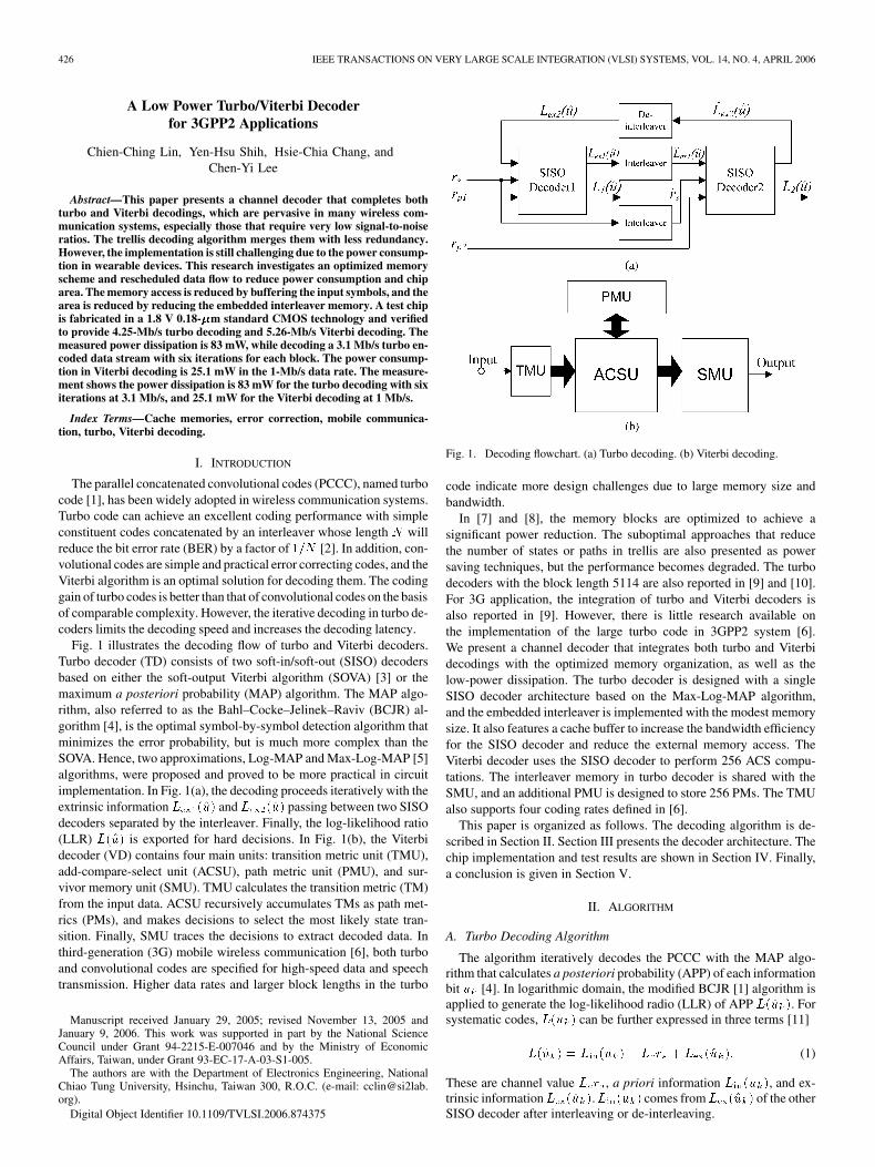
Fig. 2. Windowed MAP algorithm.
To reduce the memory requirement in SISO decoders, the slidingwindow algorithm is applied [12]. In Fig. 2, the data stream is dividedinto sub-blocks of lengthLsb, and the dummy backward recursion �1 isemployed to find the beginning of states for the true backward recursion�2. The final results are computed from �; �2, and , and the extrinsicinformation is also generated to the other SISO decoder.
B. Viterbi Algorithm
The algorithm recursively computes PMs for the shortest path termi-nating at each state. With a truncation length of T , the algorithm mustdecide a state at depth t�T by the shortest path at depth t. Besides, thetraceback approach based on the k-point even algorithm [13] is appliedfor the low-power consideration.
III. ARCHITECTURE DESIGN
The trellis decoding structure of both decoder enables the resourcesharing of the ACS and the memory units, leading to the area efficientarchitecture.
A. Turbo Decoder
Fig. 3 shows the decoder architecture in the turbo mode where theactive components are highlighted. The TD is a single SISO decoder ar-chitecture consisting of three ACS groups for �; �1 and �2 recursionsin Fig. 2, and each ACS group contains eight ACS units. The SISOdecoder processes three consecutive sub-blocks concurrently for dif-ferent strategies in the windowed MAP algorithm. ACS-� carries outthe forward recursion and saves the results in SRAM-�. ACS-�2 startsbackward recursion from the state previously determined by ACS-�1.At the same time, LLR unit calculates the L(uk) and Lex(uk) whichis formulated in (1).
B. Cache Memory Design
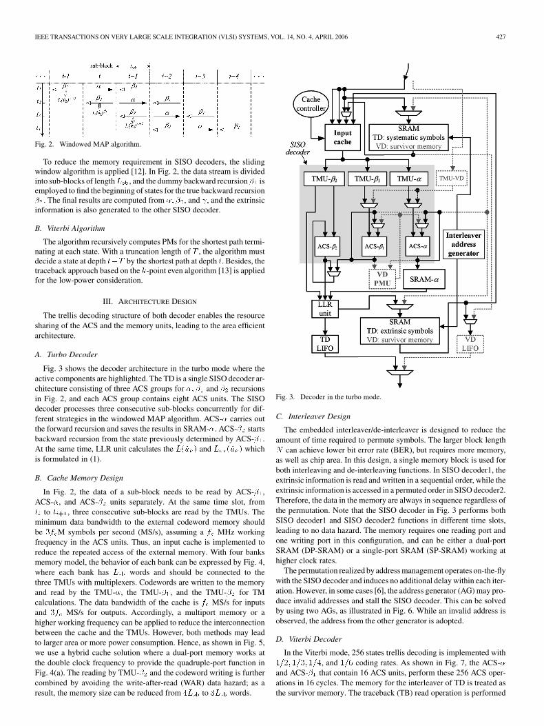
In Fig. 2, the data of a sub-block needs to be read by ACS-�1,ACS-�, and ACS-�2 units separately. At the same time slot, fromti to ti+1, three consecutive sub-blocks are read by the TMUs. Theminimum data bandwidth to the external codeword memory shouldbe 3fcM symbols per second (MS/s), assuming a fc MHz workingfrequency in the ACS units. Thus, an input cache is implemented toreduce the repeated access of the external memory. With four banksmemory model, the behavior of each bank can be expressed by Fig. 4,where each bank has Lsb words and should be connected to thethree TMUs with multiplexers. Codewords are written to the memoryand read by the TMU-�, the TMU-�1, and the TMU-�2 for TMcalculations. The data bandwidth of the cache is fc MS/s for inputsand 3fc MS/s for outputs. Accordingly, a multiport memory or ahigher working frequency can be applied to reduce the interconnectionbetween the cache and the TMUs. However, both methods may leadto larger area or more power consumption. Hence, as shown in Fig. 5,we use a hybrid cache solution where a dual-port memory works atthe double clock frequency to provide the quadruple-port function inFig. 4(a). The reading by TMU-�2 and the codeword writing is furthercombined by avoiding the write-after-read (WAR) data hazard; as aresult, the memory size can be reduced from 4Lsb to 3Lsb words.
Fig. 3. Decoder in the turbo mode.
C. Interleaver Design
The embedded interleaver/de-interleaver is designed to reduce theamount of time required to permute symbols. The larger block lengthN can achieve lower bit error rate (BER), but requires more memory,as well as chip area. In this design, a single memory block is used forboth interleaving and de-interleaving functions. In SISO decoder1, theextrinsic information is read and written in a sequential order, while theextrinsic information is accessed in a permuted order in SISO decoder2.Therefore, the data in the memory are always in sequence regardless ofthe permutation. Note that the SISO decoder in Fig. 3 performs bothSISO decoder1 and SISO decoder2 functions in different time slots,leading to no data hazard. The memory requires one reading port andone writing port in this configuration, and can be either a dual-portSRAM (DP-SRAM) or a single-port SRAM (SP-SRAM) working athigher clock rates.
The permutation realized by address management operates on-the-flywith the SISO decoder and induces no additional delay within each iter-ation. However, in some cases [6], the address generator (AG) may pro-duce invalid addresses and stall the SISO decoder. This can be solvedby using two AGs, as illustrated in Fig. 6. While an invalid address isobserved, the address from the other generator is adopted.
D. Viterbi Decoder
In the Viterbi mode, 256 states trellis decoding is implemented with1=2; 1=3; 1=4, and 1=6 coding rates. As shown in Fig. 7, the ACS-�and ACS-�1 that contain 16 ACS units, perform these 256 ACS oper-ations in 16 cycles. The memory for the interleaver of TD is treated asthe survivor memory. The traceback (TB) read operation is performed
428 IEEE TRANSACTIONS ON VERY LARGE SCALE INTEGRATION (VLSI) SYSTEMS, VOL. 14, NO. 4, APRIL 2006
Fig. 4. Multibank cache model.
Fig. 5. Quadruple-port cache memory architecture.
separately from ACS operations due to the limited memory bandwidthand takes an additional two cycles based on the 3-point even algorithm[13], [14]. The decode read follows the second traceback read and out-puts a decoded bit.
The decoding flow is illustrated in Fig. 8. On average, to decode onedata bit, it takes 19 cycles where the ACS units take 16 cycles to writenew decisions, the TB read operation spends two cycles, and the decoderead operation needs one cycle. In a 100-MHz clock rate, the Viterbidecoder can achieve the maximum throughput of 5.26 Mb/s.
Fig. 6. Removal of invalid addresses with two AGs.
Fig. 7. Decoder in the Viterbi mode.
Fig. 8. Timing diagram of the Viterbi decoder.
IV. CHIP IMPLEMENTATION
fter fixed-point analysis [15], we provide the fixed representations ofthe turbo decoder in Table I; the notation ni:nf indicates the symbolis (ni +nf ) bits with ni integer bits and nf fractional bits. Moreover,in the VD, the word length of PMs and soft input are determined to be10 and 4 bits, respectively. The BER performance is shown in Fig. 9.The decoder was implemented in the 0.18-�m standard CMOS tech-nology. In the TD mode, the sub-block length Lsb is set to 20, andtwo clock domains are used in the memory and the datapath, respec-tively. Since the double clock rate provides the memory with higherbandwidth, the single-port memory is sufficient in the proposed designexcept the cache memory.
The specification report shows the dual-port memory in Fig. 5 is0.103 mm2, leading to a 30% area reduction from Fig. 4, whose area is0.146 mm2. Two SP-SRAMs of 20 730 words are included in the de-coder for the systematic and the extrinsic data. The input and the output
IEEE TRANSACTIONS ON VERY LARGE SCALE INTEGRATION (VLSI) SYSTEMS, VOL. 14, NO. 4, APRIL 2006 429
TABLE ISUMMARY OF FIXED REPRESENTATION IN TURBO DECODING
Fig. 9. BER performance of the decoder.
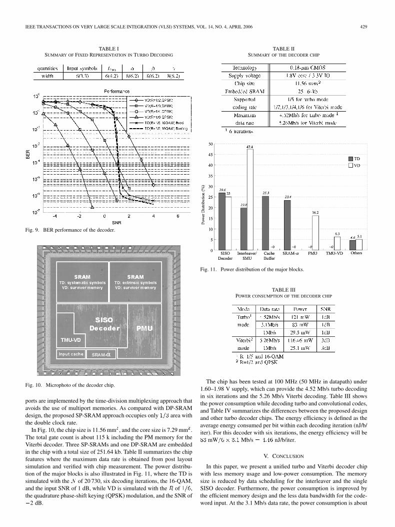
Fig. 10. Microphoto of the decoder chip.
ports are implemented by the time-division multiplexing approach thatavoids the use of multiport memories. As compared with DP-SRAMdesign, the proposed SP-SRAM approach occupies only 1=3 area withthe double clock rate.
In Fig. 10, the chip size is 11.56 mm2, and the core size is 7.29 mm2.The total gate count is about 115 k including the PM memory for theViterbi decoder. Three SP-SRAMs and one DP-SRAM are embeddedin the chip with a total size of 251.64 kb. Table II summarizes the chipfeatures where the maximum data rate is obtained from post layoutsimulation and verified with chip measurement. The power distribu-tion of the major blocks is also illustrated in Fig. 11, where the TD issimulated with the N of 20 730, six decoding iterations, the 16-QAM,and the input SNR of 1 dB, while VD is simulated with the R of 1=6,the quadrature phase-shift keying (QPSK) modulation, and the SNR of�2 dB.
TABLE IISUMMARY OF THE DECODER CHIP
Fig. 11. Power distribution of the major blocks.
TABLE IIIPOWER CONSUMPTION OF THE DECODER CHIP
The chip has been tested at 100 MHz (50 MHz in datapath) under1.60–1.98 V supply, which can provide the 4.52 Mb/s turbo decodingin six iterations and the 5.26 Mb/s Viterbi decoding. Table III showsthe power consumption while decoding turbo and convolutional codes,and Table IV summarizes the differences between the proposed designand other turbo decoder chips. The energy efficiency is defined as theaverage energy consumed per bit within each decoding iteration (nJ/b/iter). For this decoder with six iterations, the energy efficiency will be83 mW=6� 3:1 Mb/s = 4:46 nJ/b/iter.
V. CONCLUSION
In this paper, we present a unified turbo and Viterbi decoder chipwith less memory usage and low-power consumption. The memorysize is reduced by data scheduling for the interleaver and the singleSISO decoder. Furthermore, the power consumption is improved bythe efficient memory design and the less data bandwidth for the code-word input. At the 3.1 Mb/s data rate, the power consumption is about
430 IEEE TRANSACTIONS ON VERY LARGE SCALE INTEGRATION (VLSI) SYSTEMS, VOL. 14, NO. 4, APRIL 2006
TABLE IVCOMPARISON OF DIFFERENT TURBO DECODER CHIP
83 mW in decoding a turbo code with the block length of 20 730. Thechip is also designed to work reliably with the wider supply voltagerange.
ACKNOWLEDGMENT
The authors would like to thank the National Chip ImplementationCenter for chip measurement assistance.
REFERENCES
[1] C. Berrou, A. Glavieux, and P. Thitimajshima, “Near shannon limiterror-correcting coding and decoding: Turbo-codes,” in Proc. IEEE Int.Conf. Commun., 1993, pp. 1064–1070.
[2] S. Benedetto and G. Montorsi, “Unveiling turbo-codes: Some resultson parallel concatenated coding schemes,” IEEE Trans. Inf. Theory,vol. 42, no. 2, pp. 409–428, Mar. 1996.
[3] J. Hagenauer and P. Hoeher, “A Viterbi Algorithm with soft-decisionoutputs and its applications,” in Proc. IEEE GLOBECOM, 1989, pp.47.11–47.17.
[4] L. R. Bahl, J. Cocke, F. Jelinek, and J. Raviv, “Optimal decoding oflinear codes for minimizing symbol,” IEEE Trans. Inf. Theory, vol.IT-20, no. 2, pp. 284–287, Mar. 1974.
[5] P. Robertson, E. Villebrun, and P. Honher, “A comparison of optimaland suboptimal map decoding algorithms operating in the log domain,”in Proc. IEEE Int. Conf. Commun., 1995, pp. 1009–1013.
[6] Physical Layer Standard for cdma2000 Spread Spectrum Systems,3GPP2 Std. C.S0002-C, 2002.
[7] G. Masera, M. Mazza, G. Piccinini, F. Viglione, and M. Zamboni, “Ar-chitectural strategies for low-power VLSI turbo decoders,” IEEE Trans.Very Large Scale Integr. (VLSI) Syst., vol. 10, no. 3, pp. 279–285, Jun.2002.
[8] C. Schurgers, F. Catthoor, and M. Engels, “Memory optimization ofmap turbo decoder algorithms,” IEEE Trans. Very Large Scale Integr.(VLSI) Syst., vol. 9, no. 2, pp. 305–312, Apr. 2001.
[9] M. A. Bickerstaff, D. Garrett, T. Prokop, C. Thomas, B. Widdup, G.Zhou, L. M. Davis, G. Woodward, C. Nicol, and R. H. Yan, “A unifiedturbo/Viterbi channel decoder for 3 GPP mobile wireless in 0.18 umCMOS,” IEEE J. Solid-State Circuits, vol. 37, no. 11, pp. 1555–1564,Nov. 2002.
[10] M. Bickerstaff, L. Davis, C. Thomas, D. Garrett, and C. Nicol, “A 24Mb/s radix-4 log MAP turbo decoder for 3GPP-HSDPA mobile wire-less,” in IEEE Int. Solid-State Circuit Conf. Dig. Tech. Papers, 2003,pp. 151–484.
[11] J. Hagenauer, E. Offer, and L. Papke, “Iterative decoding of binaryblock and convolutional codes,” IEEE Trans. Inf. Theory, vol. 42, no.2, pp. 429–445, Mar. 1996.
[12] S. A. Barbulescu, “Iterative Decoding of Turbo Codes and OtherConcatenated Codes,” Ph.D. dissertation, Univ. South Australia,Adelaide , Australia, 1996.
[13] G. Feygin and P. Gulak, “Architectural tradeoffs for survivor sequencememory management in Viterbi decoders,” IEEE Trans. Commun., vol.41, no. 3, pp. 425–429, Mar. 1993.
[14] C. C. Lin, Y. H. Shih, H. C. Chang, and C. Y. Lee, “Design of apower-reduction Viterbi decoder for WLAN applications,” IEEE Trans.Circuits Syst. I, Reg. Papers, vol. 52, no. 6, pp. 1148–1156, Jun. 2005.
[15] Y. Wu, B. D. Woener, and T. K. Blankenship, “Data width require-ments in SISO decoding with modulo normalization,” IEEE Trans.Commun., vol. 49, no. 11, pp. 1861–1868, Nov. 2001.
Leakage-Suppressed Clock-Gating Circuit With ZigzagSuper Cut-Off CMOS (ZSCCMOS) for Leakage-Dominant
Sub-70-nm and Sub-1-V- LSIs
Kyeong-Sik Min, Hun-Dae Choi, H.-Y. Choi,Hiroshi Kawaguchi, and Takayasu Sakurai
Abstract—As a candidate for the clock-gating scheme, Zigzag SuperCut-off CMOS (ZSCCMOS) has proposed to reduce not only the switchingpower but also the leakage power. Due to its fast wakeup nature, the ZSC-CMOS can be best suited to the clock-gating scheme. The wakeup time ofthe ZSCCMOS is estimated to be 12 times faster than the conventionalSuper Cut-off CMOS (SCCMOS) in 70-nm process technology. From themeasurement of wakeup time in 0.6- m technology, it is observed to beeight times faster than the conventional scheme. Layout area, power, anddelay overhead of the ZSCCMOS are discussed and analyzed in this paper.
Index Terms—Clock-gating circuit, leakage suppression circuit,low-power circuit, Super Cut-off CMOS (SCCMOS), Zigzag SuperCut-off CMOS (ZSCCMOS).
I. INTRODUCTION
As CMOS technology is scaled down and the supply voltages(VDDs) are further decreased, the threshold voltages (VTHs) shouldalso be scaled down to prevent speed degradation. Decreasing VTH by0.1 V, however, will increase the subthreshold leakage by more thanten times. Assuming a high-performance device and one million gatesin a chip, the chip leakage can reach as much as 40 mA, even in thesleep mode [1]. This large leakage is unacceptable in most portableapplications [2].
Of the existing leakage reduction schemes, the Super Cut-off CMOS(SCCMOS) can be used below 1 V VDD without severe speed degra-dation because the power switch is made with a low-VTH MOSFET.For example, the SCCMOS in [3] can suppress the leakage down toa 1 pA-order per gate when VDD = 0:8 V. Although the SCCMOSsuccessfully suppresses the sleep-mode leakage, the wakeup time is solong that it cannot be used for the active mode. In the active mode, afast wakeup time is needed to maintain the normal operating speed.The wakeup time of the SCCMOS, amounts up to several clock cy-cles. In addition, a high -rush current may arise at this transition. Thelong wakeup time and high rush current make the SCCMOS difficultto use in the active mode where the wakeup occurs frequently. If theSCCMOS is used in the active mode, the several clock cycles of thewakeup process are stolen many times and the overall performance inthe active mode is degraded severely.
To overcome the wakeup issues of the SCCMOS, Zigzag-Super-Cut-off CMOS (ZSCCMOS) scheme with a fast wakeup has been pro-posed and this scheme successfully realizes the clock-gating schemethat saves both the switching and leakage components of power dis-sipation [4]. The conventional clock gating saves switching power byturning off the local clock whenever the block is not in use. For ex-ample, an MPEG-4 decoder chip reportedly saves 72% of the switching
Manuscript received September 15, 2004; revised March 25, 2005 and July14, 2005. This work was supported in part by the Mirai-Kaitaku project, Japan,and by the Basic Research Program of KOSEF, Korea under Grant R01-2003-000-11639-0.
K.-S. Min, H.-D. Choi, and H.-Y. Choi are with the School of Electrical Engi-neering, Kookmin University, Seoul 136-702, Korea (e-mail: [email protected]).
H. Kawaguchi was with the Institute of Industrial Science, Center for Col-laborative Research, University of Tokyo, Tokyo 153-8505, Japan. He is nowwith the Department of Computer Systems Engineering, Kobe University, Kobe657-8501, Japan.
T. Sakurai is with the Institute of Industrial Science, Center for CollaborativeResearch, University of Tokyo, Tokyo 153-8505, Japan.
Digital Object Identifier 10.1109/TVLSI.2006.874378