Embed Size (px)
Citation preview
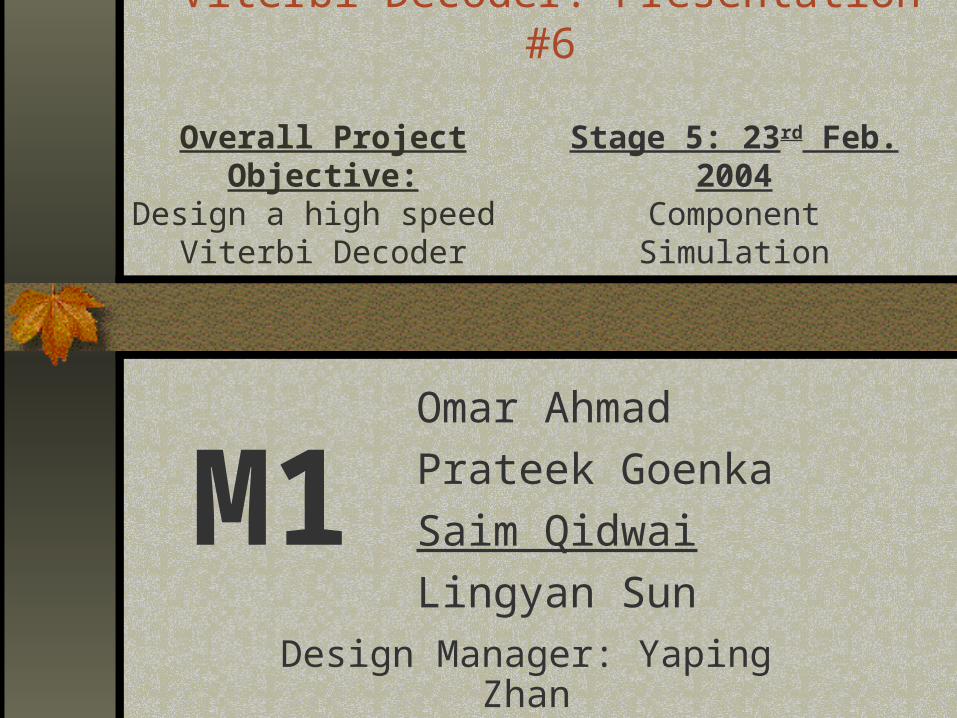
Viterbi Decoder: Presentation #6
M1
Overall Project Objective:
Design a high speed Viterbi Decoder
Stage 5: 23rd Feb. 2004
Component Simulation
Design Manager: Yaping Zhan
Omar Ahmad
Prateek Goenka
Saim Qidwai
Lingyan Sun
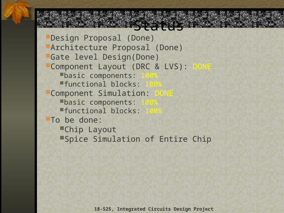
Status
18-525, Integrated Circuits Design Project
Design Proposal (Done)Architecture Proposal (Done)Gate level Design(Done)Component Layout (DRC & LVS): DONE
basic components: 100%functional blocks: 100%
Component Simulation: DONEbasic components: 100%functional blocks: 100%
To be done:Chip LayoutSpice Simulation of Entire Chip
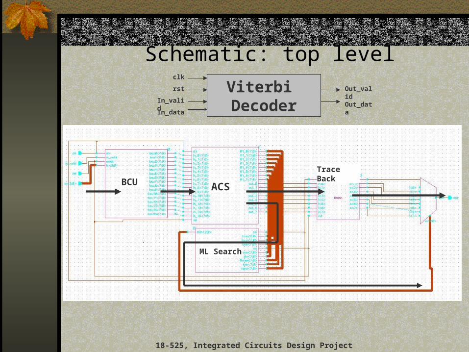
Schematic: top level
18-525, Integrated Circuits Design Project
Viterbi Decoder
clk
rst
In_valid
In_data
Out_valid
Out_data
BCU ACS
Trace Back
ML Search
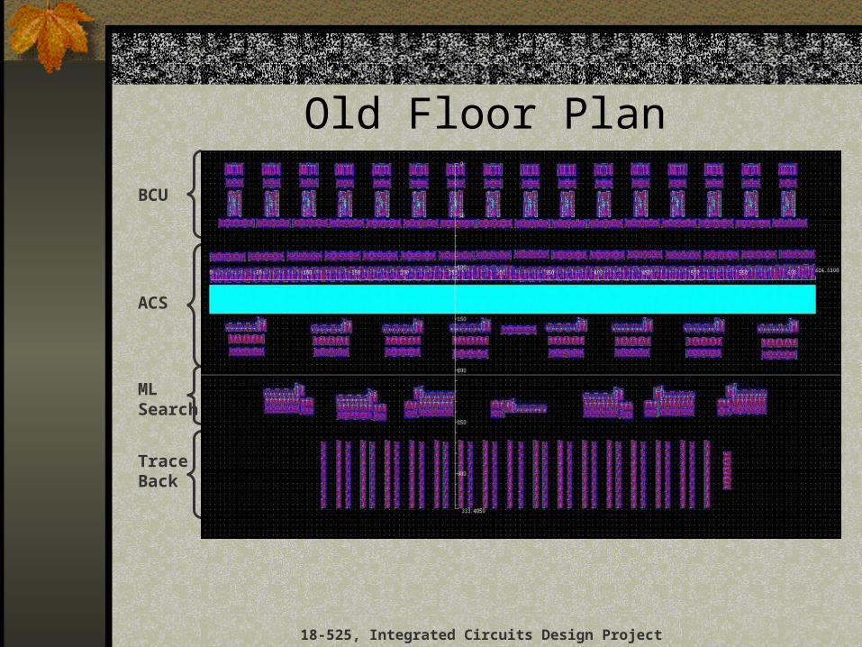
Old Floor Plan
BCU
ACS
ML Search
Trace Back
18-525, Integrated Circuits Design Project
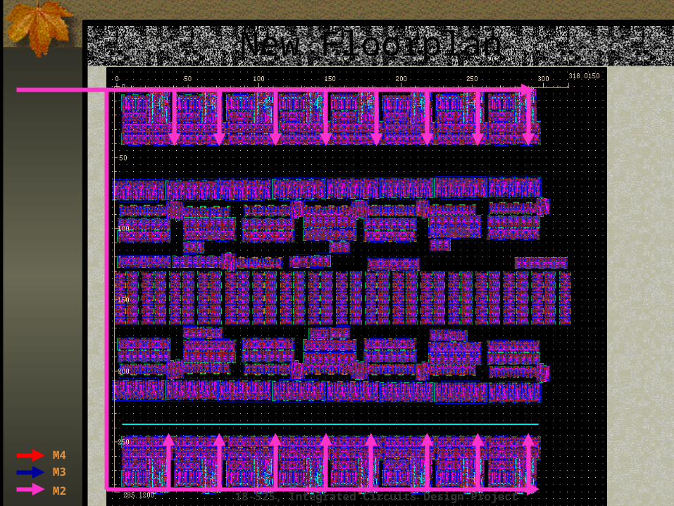
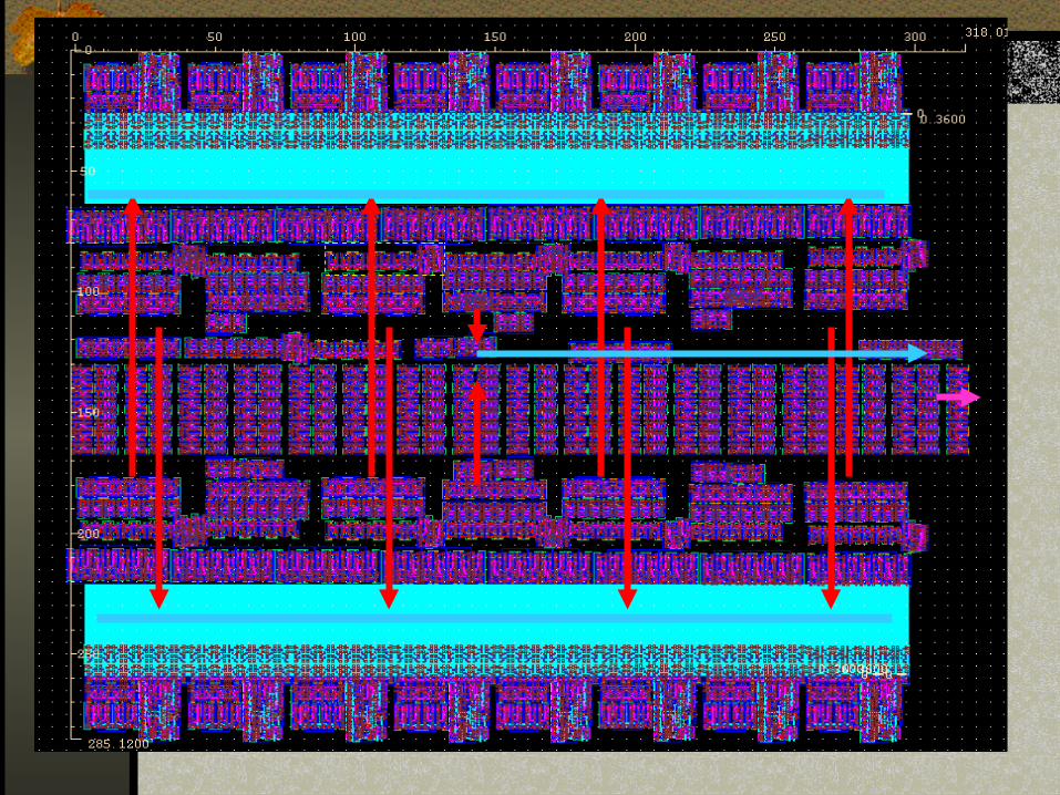
New Floorplan
18-525, Integrated Circuits Design Project
M4
M2
M3
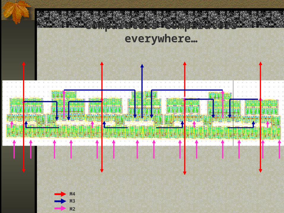
Comparators Comparators everywhere…
M4
M2
M3
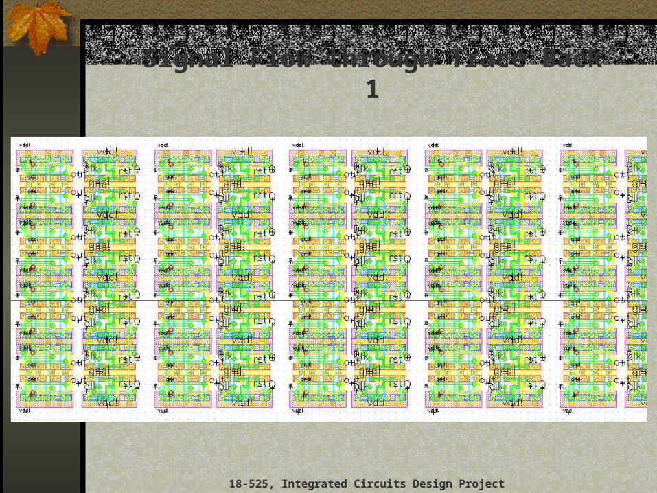
Signal Flow through Trace Back 1
18-525, Integrated Circuits Design Project
Signal Flow through Trace Back 1
18-525, Integrated Circuits Design Project
Mux
Mux
Mux
Mux
Mux
Mux
Mux
Mux
Flip-Flop
Flip-Flop
Flip-Flop
Flip-Flop
Flip-Flop
Flip-Flop
Flip-Flop
Flip-Flop
Signal Flow through Trace Back 2
18-525, Integrated Circuits Design Project
Mux
Mux
Mux
Mux
Mux
Mux
Mux
Mux
FF
FF
FF
FF
FF
FF
FF
FF
Mux
Mux
Mux
Mux
Mux
Mux
Mux
Mux
FF
FF
FF
FF
FF
FF
FF
FF
Mux
Mux
Mux
Mux
Mux
Mux
Mux
Mux
FF
FF
FF
FF
FF
FF
FF
FF
…
…
…
…
…
…
…
…
Adder 8bPropagation Delay
18-525, Integrated Circuits Design ProjectWorst Case: 1.44 ns
Adder 8bRising and Falling Transitions
18-525, Integrated Circuits Design Project
Rising Time: 390ps. Falling Time: 238ps.
18-525, Integrated Circuits Design Project
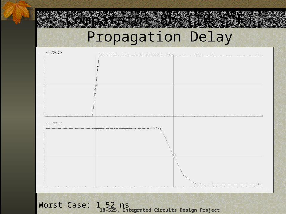
Comparator 8b (10 f F)Propagation Delay
Worst Case: 1.52 ns
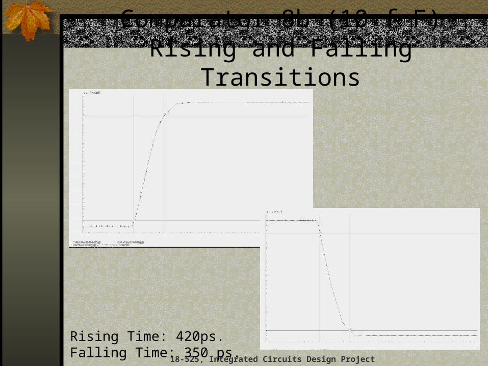
Comparator 8b (10 f F)Rising and Falling Transitions
18-525, Integrated Circuits Design Project
Rising Time: 420ps. Falling Time: 350 ps.
18-525, Integrated Circuits Design Project
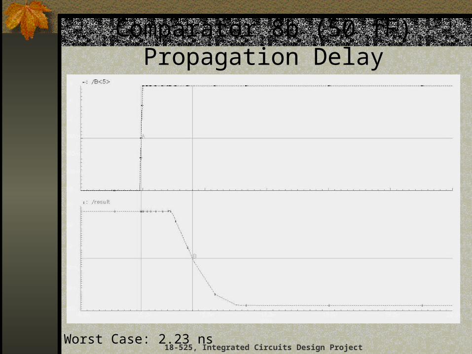
Comparator 8b (50 fF)Propagation Delay
Worst Case: 2.23 ns
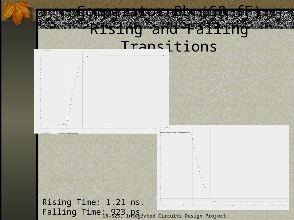
Comparator 8b (50 fF)Rising and Falling Transitions
18-525, Integrated Circuits Design Project
Rising Time: 1.21 ns. Falling Time: 923 ps.
18-525, Integrated Circuits Design Project
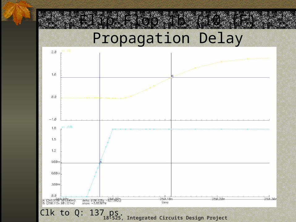
Flip Flop 1b (10 fF)Propagation Delay
Clk to Q: 137 ps.
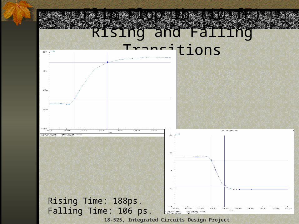
Flip Flop 1b (10 fF)Rising and Falling Transitions
18-525, Integrated Circuits Design Project
Rising Time: 188ps. Falling Time: 106 ps.

18-525, Integrated Circuits Design Project
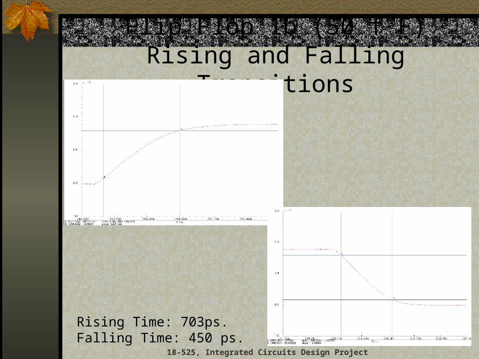
Flip Flop 1b (50 f F)Propagation Delay
Clk to Q: 405 ps.
Flip Flop 1b (50 f F)Rising and Falling Transitions
18-525, Integrated Circuits Design Project
Rising Time: 703ps. Falling Time: 450 ps.
18-525, Integrated Circuits Design Project
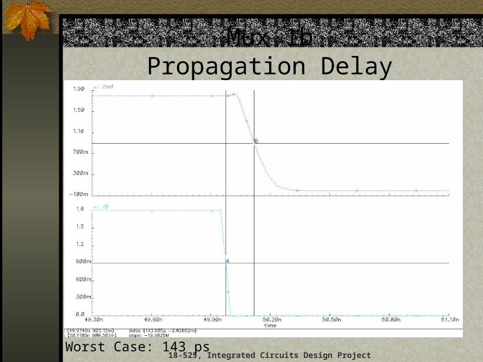
Mux 1bPropagation Delay
Worst Case: 143 ps
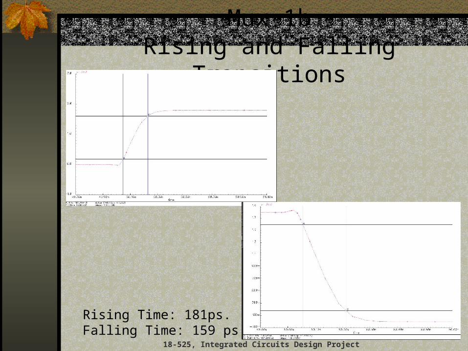
Mux 1bRising and Falling Transitions
18-525, Integrated Circuits Design Project
Rising Time: 181ps. Falling Time: 159 ps.
18-525, Integrated Circuits Design Project
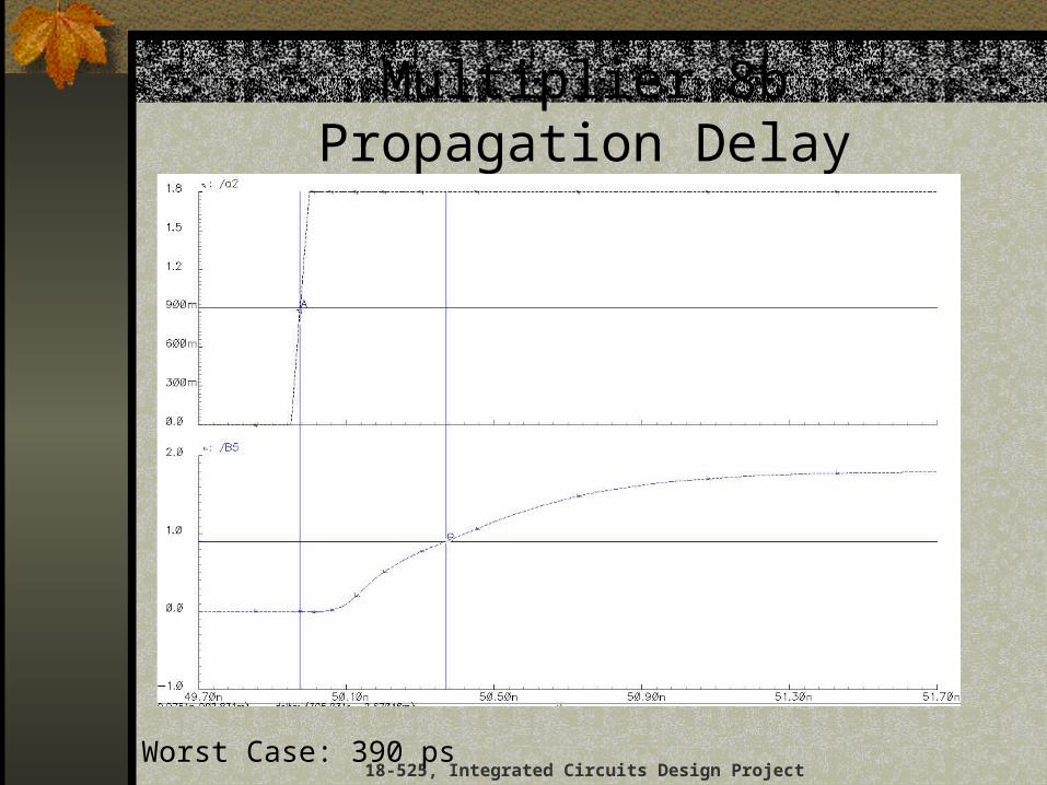
Multiplier 8bPropagation Delay
Worst Case: 390 ps
18-525, Integrated Circuits Design Project
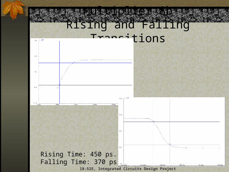
Multiplier 8bRising and Falling Transitions
Rising Time: 450 ps. Falling Time: 370 ps.
18-525, Integrated Circuits Design Project
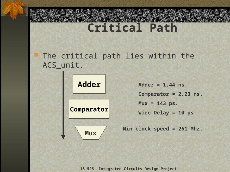
Critical Path
The critical path lies within the ACS_unit.
Adder
Comparator
Mux
Adder = 1.44 ns.
Comparator = 2.23 ns.
Mux = 143 ps.
Wire Delay = 10 ps.
Min clock speed = 261 Mhz.

18-525, Integrated Circuits Design Project
Questions?