Embed Size (px)
Citation preview

Presented By: Dale LeeE-mail: [email protected]
24 January 2008
What Can No Longer Be Ignored In Today’s Electronic
Designs

Introduction
Component packaging technology continues to decrease in size (length, width, thickness), interconnection density per unit area is increasing (thinner PCB’s, smaller lines & spaces), functional performance is increasing (thermal, mechanical, electrical) at the same time as assembly processes are changing to lead-free assembly. Because of this migration, many of the elements that use to be ignored, can no longer be ignored.

Elements of Design Process
•Cultural Differences– Religious– Race– Political
•Geographical Differences– Language– Environmental (Local/Regional)– Unit of Measure (Inch vs Metric)
•Time Line Management– Multiple Idea Selection
• Quickest To Success• Quickest To Failure
– Process Development• Nominal Vs At Limits

Electronic Designs
• Elements That Were Previously Insignificant, May Be A Significant Source of Assembly Defects
– Part Tolerance– Trace Connections– Via Hole Type– Via Hole Location– Via Pad Size Uniformity– Tooling Tolerance– Process Tolerance– Facility Environment

Component Issues - Warpage
• Higher Lead Free Solder Solidification and Process Temperatures, Increases The Amount Of Thermal Expansion Mismatch Of Components Which Can Increase Amount Of Component Warping During Assembly Process
• May Require Redesign Of Package (Material Selection) For ThermalMass And Expansion Balance.

Component Issues – Warpage & Thermal Shock
May Require Change In Production Process
• Tooling To Bridge Warpage Gap.(Increased Solder Paste Volume Application, etc.)
• Reflow Profile To Bridge Warpage Gap.(Decreased Thermal Change Rate – Reduce Surface
To Cooler Location Temperature Delta - TCE Induced Warpage)
• Reflow Profile To Reduce Micro Cracks In Multilayer Ceramic Capacitor Chips & Arrays.
(Decreased Thermal Change Rate – Reduce Surface To Cooler Location Temperature Delta For Chip > 1210)

Component/PCB Warpage Impacts
Split Planes/Unused Pad Removal:
• Localize Changes In Thickness/CoplanarityOf PCB
• Potential Opens From Tilted Components (Teeter-Totter Effect)
• Potential Opens From “Dropped” Solder Connection
• Potential Reduced Reliability From Stretched Solder Joints

Trace Routing Impacts Solder Joint
Increased Mounting Pad Size Affected By:
• Number Of Trace Connections To Each Pad
• Width Of Trace Connections To Each Pad
• Size of Pad – Small Pads Have Less
Margin• Uniformity Of Trace Egress
Direction – Some Package Types Are
More Sensitive Than Others• Uniformity Of Trace Sizes
EFFECTIVE PAD SIZE ANALYSIS
0
10
20
30
40
50
60
4 10 15 20WIDTH OF TRACE
% P
AD S
IZE
INCR
EAS
E
10 Mil Nom 15 Mil Nom 20 Mil Nom
10 Mil Max 15 Mil Max 20 Mil Max

Trace Routing Impacts Solder Joint
• Gradient Of Different Trace Sizes• Localized Concentrated Large Trace
Connections Increase Defect Potential
• Concentrations Of Design Variability Can Create:Solder Bridge, Open Connection, Insufficient Solder, Tilted Components

Micro-Via in Pad
Micro-Via Locations Should Be Consistent– Area Array Components - Center of
Pad – Leadless (Chips, Chip Array, LCC,
QFN, etc) and Leaded (QFP, SOIC, SOT, etc.) Components – Near Toe Fillet
X-ray Image

Micro-Via in Pad
• Voids in Solder Joints– Unfilled Via in Pad
• Provide Flat Pad With Filled/Plated Closed Via
• Solder Joint Formation– Thermal Connection
• Plane Connection
• Multiple Connections
• Stacked Via
– Solder Volume• Via Location - Edge Unfilled Via Plated Closed Via Filled Via

High Design Density
Spacing Limitations Are Not A Driven By The Manufacturing/Assembly Process
SMT Pads• Minimum Or No Visible Solder (Toe) Fillets
– Potential AOI/Inspection Issue
Component Spacing• Minimum Component to Component Spacing
– Limited/No Rework
– Limited AOI/Test Point Access

Component Pad - Thermal Imbalance
• Multiple Trace Connections– Number Of Trace Connections
Per Pad– Uniformity Across All Pads On
Single Component• Solder Mask Defined Pad• Increased Soldering Defects
– Delayed Reflow Across SMT Components
• Tombstone Components• “Ball in Socket” Area Array
Component

Solder Paste Printing Volume
Open/Unwetted LGA Solder Connection
Leadless Device Usage Increase (DFN, QFN, LCC LGA) & Ultra-fine Pitch Components Impacts:
• Tighter Tolerance On Solder Paste Volume – Thinner Stencil
• Increased Uniformity Of Paste Volume Across Component (Pad to Pad)
• Paste Volume/Pad Trace Egress Direction Impact– Some Package Types Are
More Sensitive Than Others

Interconnection Failure Mode Shift
• Courtesy of Universal Instruments

PCB Performance Consideration
• Performance Requirements May Dictate Material Selection– Mission Critical Applications; Military, Aerospace, Medical
• Decisions Should Be Conservative To Allow For A Safety Zone
– Non Fault Tolerant Systems Where Additional Reliability Requirements Are Specified
• Mainframes, Servers, Communications Equipment, Automotive
– Life Expectancy Of The Product• Consumer Electronics Vs. System Electronics
– System Environment• Additional Performance Criteria Such As CAF Resistance May Make
Certain Materials More Appropriate
• Photos Courtesy of Universal Instruments

PCB Lead Free Laminate
• Traditional DICY Cured FR4 Laminates Cannot Survive Multiple Elevated Pb Free Reflow Profiles Or Sustain Impact To Reliability– Tg Alone Is Not An Indicator Of Lead Free Capability– T260 And T288 Values Alone Do Not Assure Lead Free
Capability Of A Laminate System– Base Resin Decomposition Temperature (Td) And CTE
Values Are Good Indicators Of Lead Free Survivability
• Reliability Impacts Following Assembly Simulation Critical– Reflow Conditions Will Vary Depending Upon Board Design– Board Design Contributes To The Lead Free Equation – Electrical Properties Need To Be Accounted For In Design
• Resin Content – Changes Electrical Performance• Halide Free – Change Electrical Performance and Moisture
Absorption
• Photos Courtesy of Cookson and Universal Instruments

Internal PCB Impacts
• Copper Plane– Uniform Thickness – Balanced Thickness To PCB
Centerline
• Thicker Copper Plane Layers Increase Thermal Mass– Thinner Is Better– Increase Thermal Pad Isolation
• Issues Include:– PCB Warping– PTH Hole Fill
1 Oz
2 Oz

Internal PCB Impacts
• Number Of Layer Connections to Plated Through Hole– Increased Number Of Layer
Connections Increases Thermal Mass Of Plated Through Hole
– Increased Number Of Plane Layer Connections Greatly Increases Thermal Mass Of Plated Through Hole
– Increase Thermal Pad Isolation To Improve Solder Flow To Topside
• Issues Include:– PTH Hole Fill

What To Do?
• Increase Solder Temperature?
• Lead Free Solder Issue• Higher Solder Temperatures Or
Increased Solder Dwell Times Create Problems With Pads On Solder Side
* Dr. S. Zweiger, Solectron GMBH, Productronica Green Day, November 2005
Wave Solder & Rework Issues
• PCB Photo Courtesy of Cookson – Alpha Metals• Byle, et al, “Copper Dissolution Rate in Pb-Free Soldering Fountain Systems”, SMTA-I 2006
Limit Effects Of Copper Dissolution
– Use Lower Dissolution Rate Solder Alloy
• Modified SAC Alloy (Sb, Ni, Zn, Ge, In, Etc)
• Non-SAC Alloy (Sn/Cu/Ni, Etc)
– Pad Trace Connection• Tear Drop
• Snow Man Connection
• Wide Trace– Greater Than 0.010” 0.005” Trace Dissolution in
30 Seconds

Lead Free Process Impacts On Solder Mask
• Higher Reflow Temperature -Additional Stress On Solder Mask Bond Line- Potential Delamination- Discoloration - Solder Wicking Under Mask
(Improperly Cured)
Properly Cured Improperly Cured
“Board Challenges (and Solutions) For Next Generation Designs, J. Fix, Taiyo America, Webinar, May, 2006

Solder Mask Selection Impact
• A Low Surface Energy “Glossy” Finish Can Generate Solder Defects Similar In Appearance Of No Flux Or Too Little Flux On The Board.
• Resulting in Whiskers, Strings, Peaks, Bridges, Icicles, Solder Balls, Solder Web, Solder Flags

Lead Free Solder Advantages
• Material Costs– NO
• More Expensive
• Reflow Temperature– NO
• Higher Temperatures For Reflow & Rework
• Increased Component & PCB TCE Mismatch (Warp, Crack)
• Through Hole Soldering– NO
• Higher Hand and Rework Solder Temperature
• Greater Lead to Hole Clearance
• Increased Copper Dissolution
– Correct Placement Location and Orientation Analysis
• Assembly Process Physics– Potential
• Tighter SMT Lead Pitch Packages
• Increase Secondary Side SMT Package Mass
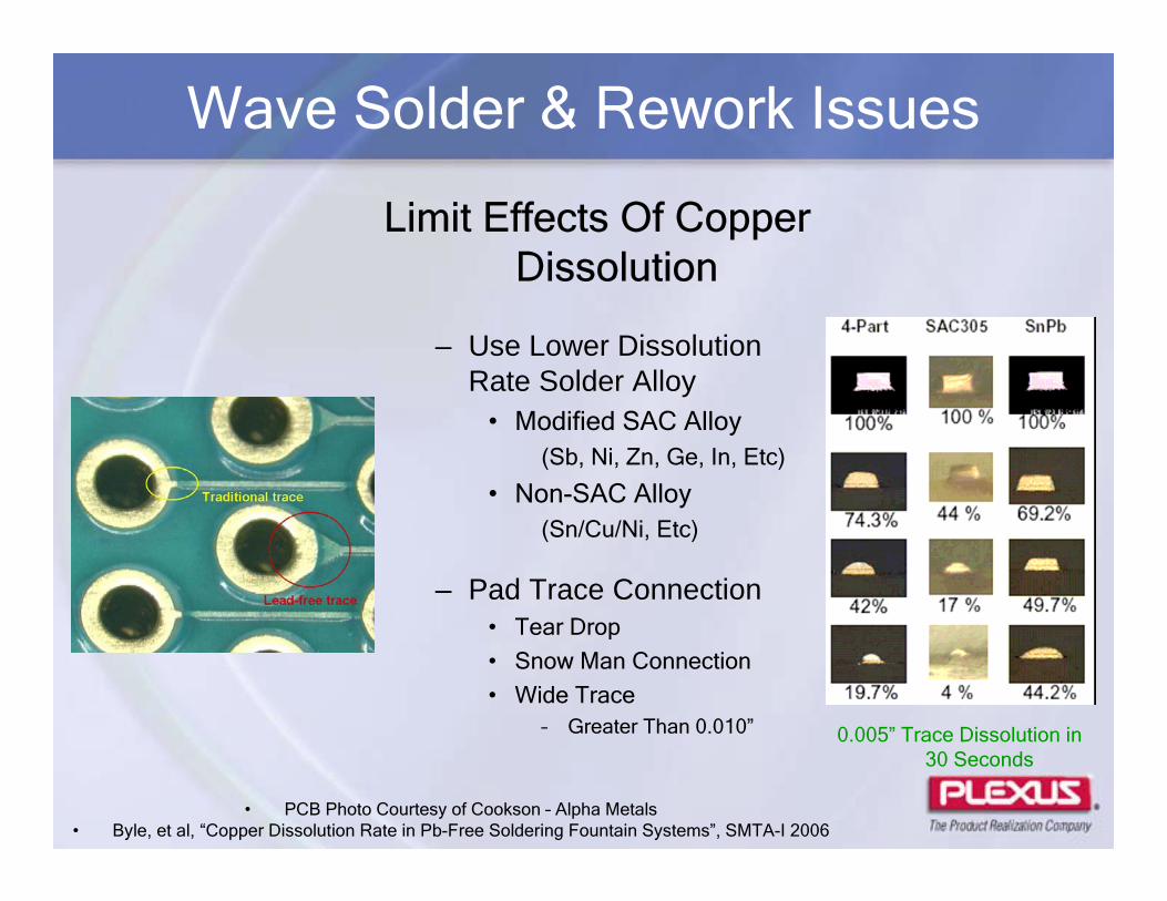
Physical Property Comparison
Alloy Sn62 SnAg3.8Cu0.7
Melting point 179C 217CDensity (g/mm2) 8.5 7.5Surface tension @ ~35 C ~460 dyne/cm* ~510 dyne/cm**
above melting point in airWetting angle on Cu (deg) 12 43
* Values for Sn63Pb37** Values for SAC305
Increase Surface Tension = Higher Mass Components on Secondary Side of Double SidedSMT Assemblies ( 10-12%)
Physical Values From: Henkel Technologies – SMTA Chapter Presentation, Orange County, Oct, 2005Surface Tension From Indium Corporation

Coalescent Performance Comparison
• Indium Corp. Pb-Free Workshop 2003
Lead-free has significantly higher coalescent force(Decrease Solder Spread)

Lead Free Solder Spread
• Stencil Alignment of Solder Paste To Pad Tolerance May Be Critical To Good Manufacturing Yields(Dependant Upon PCB
Surface Finish)
• Example – OSP Finish
Alpha Metals, SMT Mag Webcast, Jan 2006
Tin-Lead Paste
Lead Free Paste

PCB Finish Vs Solder Spread
– OSP
– Immersion Silver
– Immersion Tin
– ENIG
Amount Of Lead Free Solder Wicking Is Dependant Upon Finish

Tin-Lead Vs Lead Free Wicking
Depending Upon The Pairing Of PCB Surface Finish And Component Lead Finish, The Amount Of Solder Wicking / Spread Can Induce or Reduce Solder Defect Formation.
Lead Free Tin-Lead

Component Placement Tolerance Fallacy
• No problem “We place 0.5-mm (20 mil) pitch QFPs every day”
0.3-mm ball0.25-mm pad
Lead Width 0.2-mm
Pad Width 0.3-mm
QFP Misplaced 0.15-mm in x & y
0.5-mm CSP Misplaced 0.15-mm in x & y
Foot Length 0.76-mm
Top View
Courtesy of Xetel Corporation

Component Placement Tolerance Fallacy
0.3-mm ball
0.25-mm pad
Solder Paste Shift
Top View Profile View
Courtesy of Xetel Corporation

Match Tooling Design To Parts
• Normal Manufacturing Process Variability May Exceed Allowable Assembly Process Tolerance For High Yield, Reliable Assembly
• Matched Tooling (Stencils) To Materials (PCB) May Be Required
PCB to Stencil Pad Positional Deviation Measurements No Adjustments
PCB to Stencil Pad Positional Deviation Measurements With Scaling Adjustments

Lead To Hole Clearance
Lead Angle In Hole Combined With Lead Clearance Can Impact Void Creation In Plated Through Hole.– Lead Type Can Impact Void
Creation• Round Versus Flat Ribbon
– Lead / Hole Metallization Can Impact Void Creation
• Faster Wetting Rate = Greater Risk Of Void Creation *
K. Seelig, et al, “Lead-Free Solder Assembly For Mixed Technology Circuit Boards”, SMTA-I 2006

Lead To Hole Clearance
• Lead Free Soldering– Lead Clearance Minimum May Increase– Increasing Board Thickness May
Further Increase Lead To Hole Clearance (Aspect Ratio)
– Larger Holes Create Less Voids
• Smaller Hole To Lead Clearance Decreases Shrinkage Holes / Hot Tear Joints
IPC-A-610D, Fig. 5.67

Through Hole Pad Design
• Square Pads Should Not Be Used On Solder Side– Increased Pad Lifting*– Increased Solder Defect –
Bridge/Flag/Web
• Decrease Component / Top Side Pad Size**– Reduced Fillet Lifting
* Dr. S. Zweiger, Solectron GMBH, Productronica Green Day, November 2005
** K Puttlitz, K Stalter, “Handbook of Lead-Free Solder Technology For Microelectronic Assembly”, pp 628, Fig 48

Through-Hole Component Mounting
• Leads Should Extend Below Bottom of Board
• Lead Protrusion: Shorter is Better
– Decreased Solder Bridging– Decreased Component Tilting
• Lead Free Solder:– Lead Length Should Be Even
Shorter Than Tin-Lead Solder.

SMT Component Placement Secondary Side
– No SMT Parts Under Solder Tail Parts– No Passive Packages Smaller Than 0603 – No Passives Packages Greater Than 1210
• Lead Free Wave Soldering Maximum Component Size Is Smaller Than Tin/Lead
– No SMT QFP Packages– No Large/Tall SMT SOIC Packages on
Wave Side• May Require Increased Pad Length Extension
From Component Body• May Require Increased Component to
Component Spacing(Requires Very Long Pad Length or Spacing)
– Tighter Component Spacing Require Use Of Nitrogen

SMT Thieving Pads
Purpose Is:
To Wick Excess Solder Away From Pins
Provide Solder Wave Surface Tension Breaking Points
Direct Flow of Solder to Pins and Around Features
• Photos Courtesy of Cookson – Alpha Metals
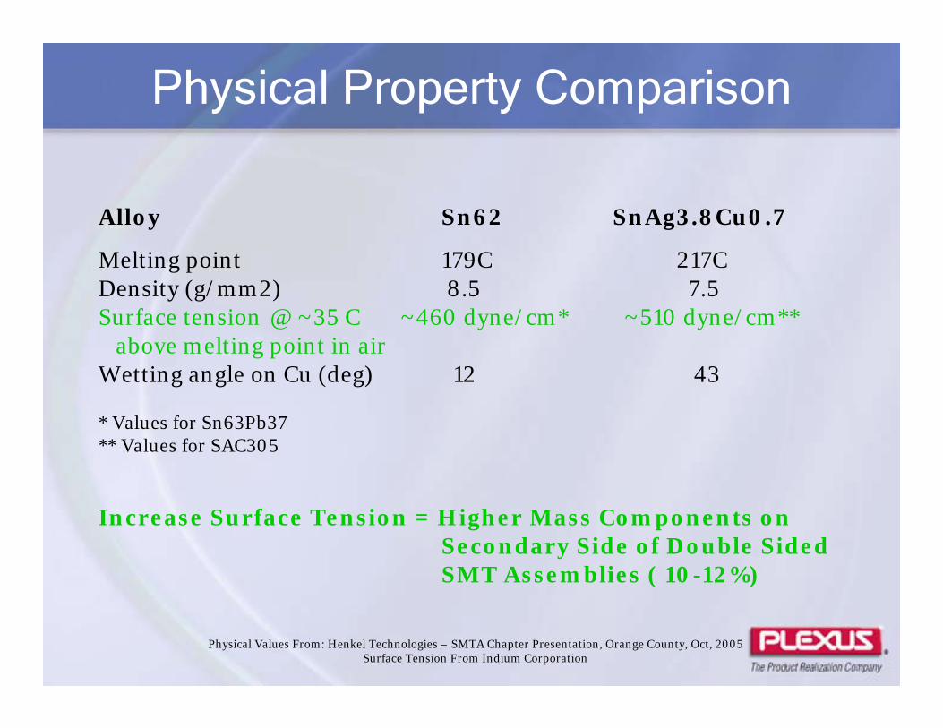
Cleaning
“Remember it is not the cleanliness of the entire board that causes the electrical failure but the amount of residue between two pads on a critical circuit the define the cleanliness of the assembly.”
Terry Munson, President/Senior Technical Consultant, Foresite
Ask the Experts, Circuitnet.com, 7 Jan. 2008

Cleaning Chemistry Compatibility
• Cleaning Chemistries Must Work With Tight Component Spacing– Component To Component Spacing– Component Stand-off Height
• Compatible With Greater Diversity Of Materials– PCB’s
• Substrate Materials• Solder Mask• Silk Screen Ink• Pad Finish
– Component Materials• Package• Seals• Marking Inks
– Solder

What is Source of Whiskers in Removed BGA Component Package Solder Joints at PCB Interface Surface?
1. Solder Paste2. Stencil Printer
3. Reflow4. PCB Finish
5. Thermal Aging
Source Of Contamination

Closing Thought
“We can’t solve problems by using the same kind of thinking we used when we created them.”
Albert Einstein
Don’t Forget About Reflow Process Induced Warpage/Coplanarity Issues.
Thank You!
Questions