Embed Size (px)
Citation preview
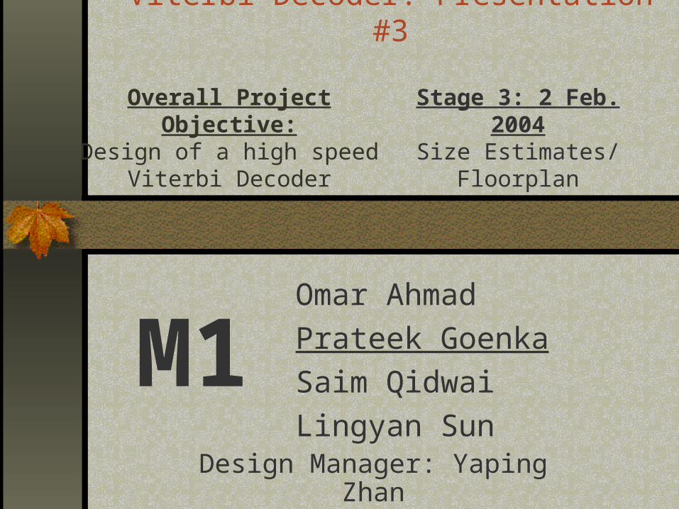
Viterbi Decoder: Presentation #3
Omar Ahmad
Prateek Goenka
Saim Qidwai
Lingyan Sun
M1
Overall Project Objective:
Design of a high speed Viterbi Decoder
Stage 3: 2 Feb. 2004
Size Estimates/ Floorplan
Design Manager: Yaping Zhan
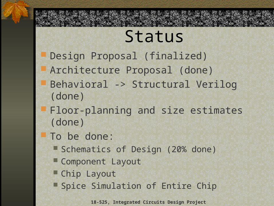
Status Design Proposal (finalized) Architecture Proposal (done) Behavioral -> Structural Verilog (done) Floor-planning and size estimates (done) To be done:
Schematics of Design (20% done) Component Layout Chip Layout Spice Simulation of Entire Chip
18-525, Integrated Circuits Design Project
18-525, Integrated Circuits Design Project
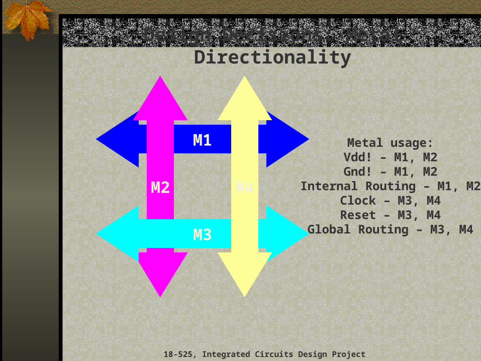
Design Decisions: Metal Directionality
M1
M2
M3
M4
Metal usage:Vdd! – M1, M2Gnd! – M1, M2
Internal Routing – M1, M2Clock – M3, M4Reset – M3, M4
Global Routing – M3, M4
18-525, Integrated Circuits Design Project
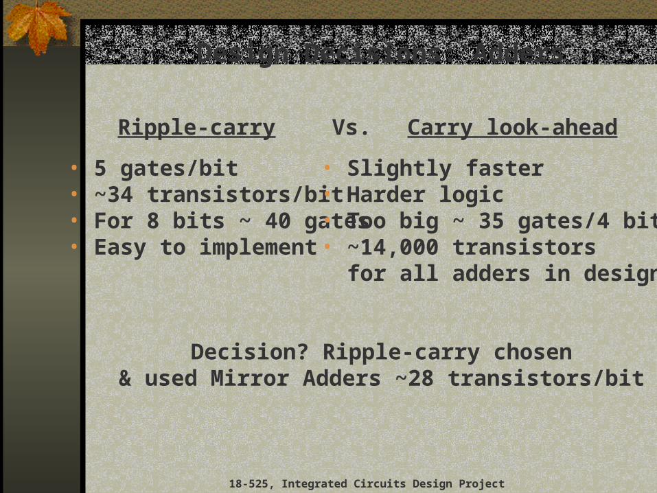
Design Decisions: Adders
Ripple-carry Carry look-aheadVs.
• 5 gates/bit• ~34 transistors/bit• For 8 bits ~ 40 gates• Easy to implement
• Slightly faster• Harder logic• Too big ~ 35 gates/4 bits• ~14,000 transistors for all adders in design
Decision? Ripple-carry chosen& used Mirror Adders ~28 transistors/bit
a7 a6 a5 a4 a3 a2 a1 a0
a7 a6 a5 a4 a3 a2 a1 a0
a0a7 a0a6 a0a5 a0a4 a0a3 a0a2 a0a1 a0a0
a1a6 a1a5 a1a4 a1a3 a1a2 a1a1 a0a1
A2a5
a2a4 a2a3 a2a2 a1a2 a0a2
a3a4 a3a3 a2a3 a1a3 a0a3
a3a4 a2a4 a1a4 a0a4
a2a5 a1a5 a0a5
a1a6 a0a6
a7 a6 a5 a4 a3 a2 a1 a0
a7 a6 a5 a4 a3 a2 a1 a0
X a0a5 a0a4 a0a3 a0a2 a0a1 0 a0
X a1a4 a1a3 a1a2 a1
X a2a3 a2
X a3
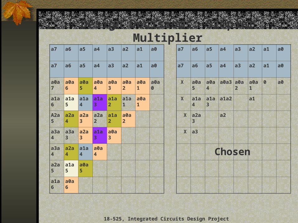
Design Decisions: Simpler Multiplier
18-525, Integrated Circuits Design Project
Chosen
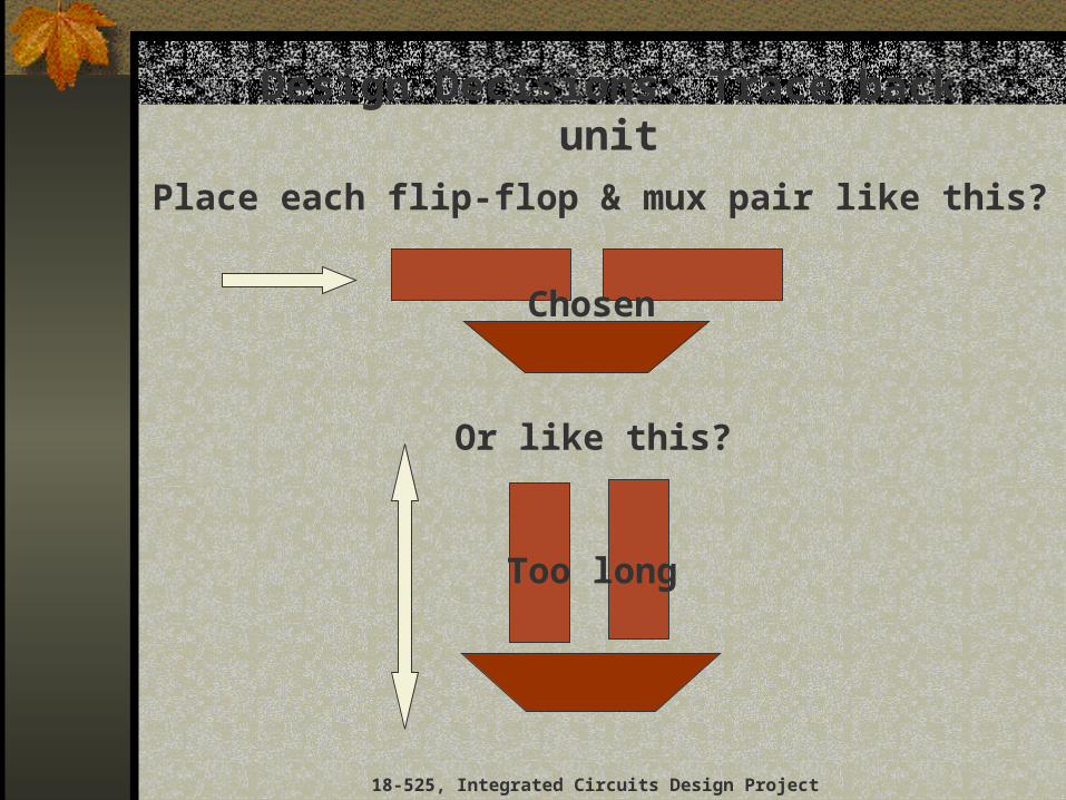
Design Decisions: Trace back unit
Place each flip-flop & mux pair like this?
Or like this?
Too long
Chosen
18-525, Integrated Circuits Design Project
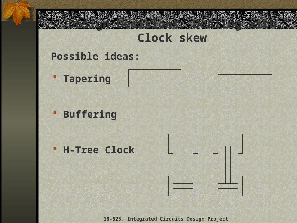
Design Decisions: Dealing with Clock skew
18-525, Integrated Circuits Design Project
Possible ideas:
Tapering
Buffering
H-Tree Clock
18-525, Integrated Circuits Design Project
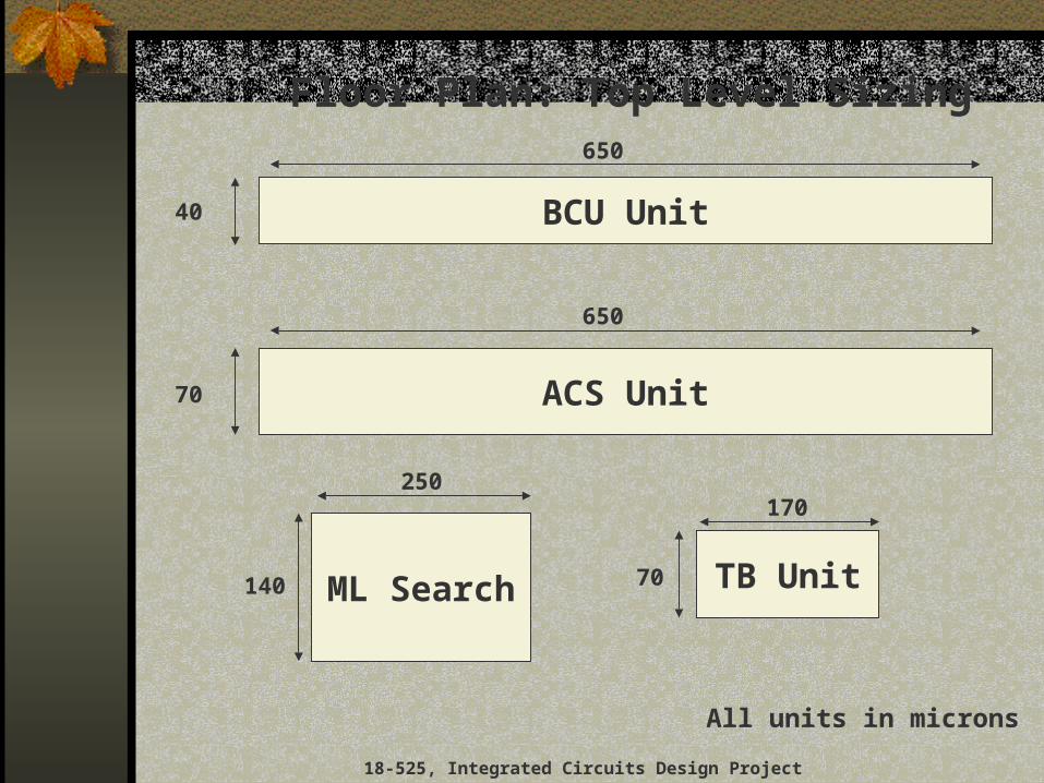
Floor Plan: Top Level Sizing
ML Search
250
140
ACS Unit
650
70
BCU Unit
650
40
TB Unit
170
70
All units in microns
18-525, Integrated Circuits Design Project
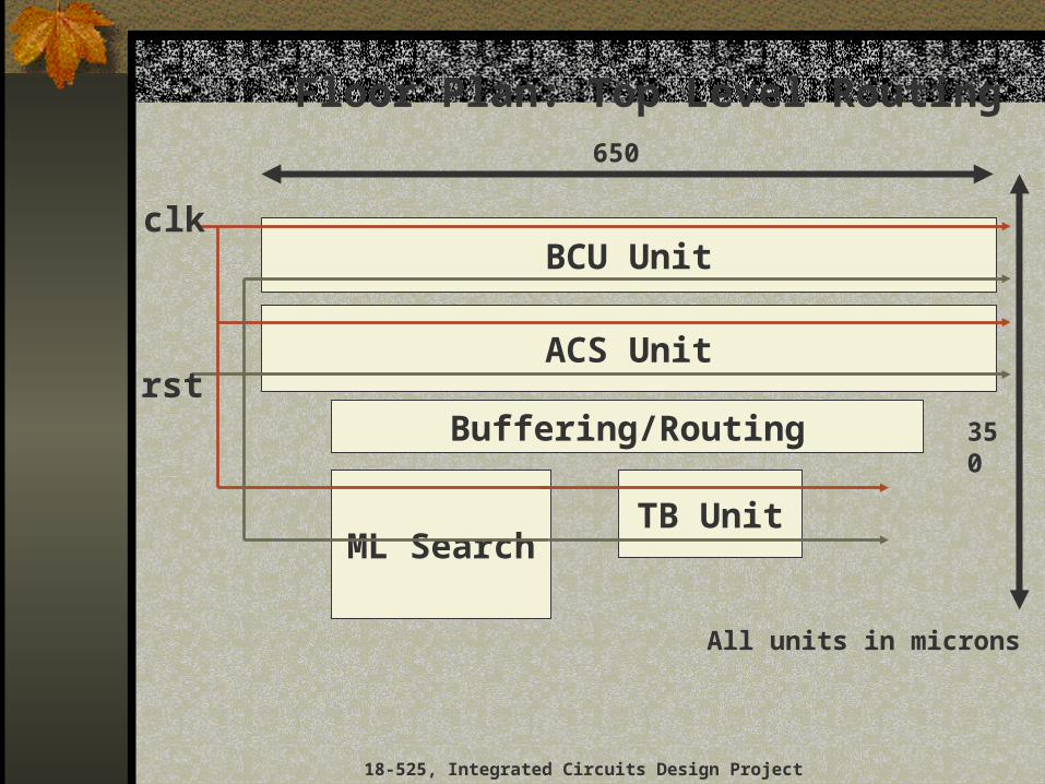
Floor Plan: Top Level Routing
ML Search
ACS Unit
BCU Unit
TB Unit
clk
rst
650
350
All units in microns
Buffering/Routing
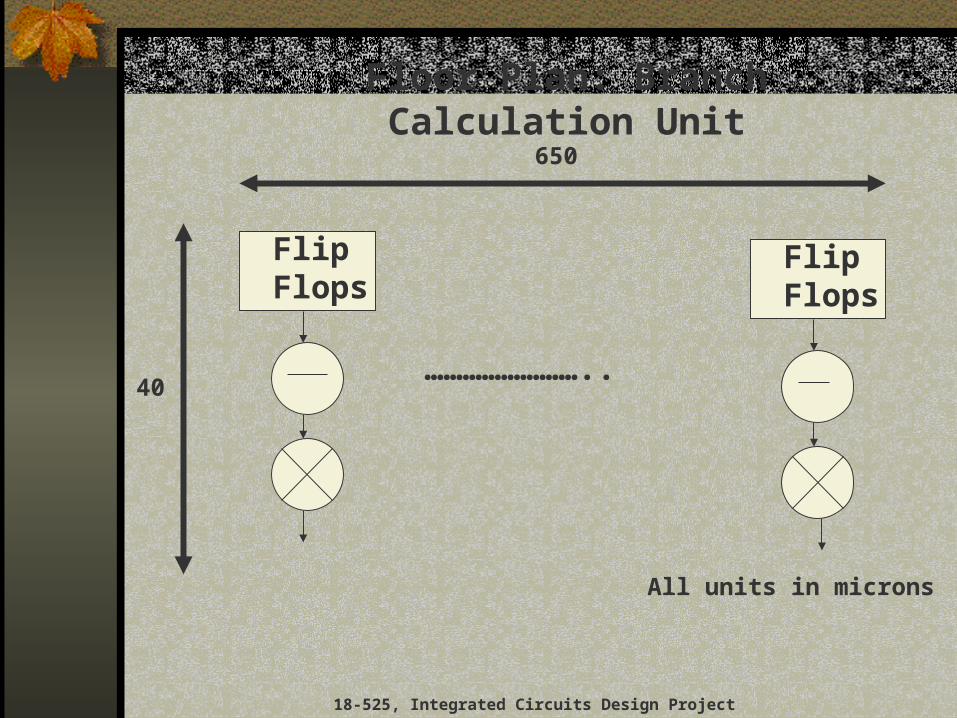
Floor Plan: Branch Calculation Unit
18-525, Integrated Circuits Design Project
Flip Flops
Flip Flops
……………………..
650
40
All units in microns
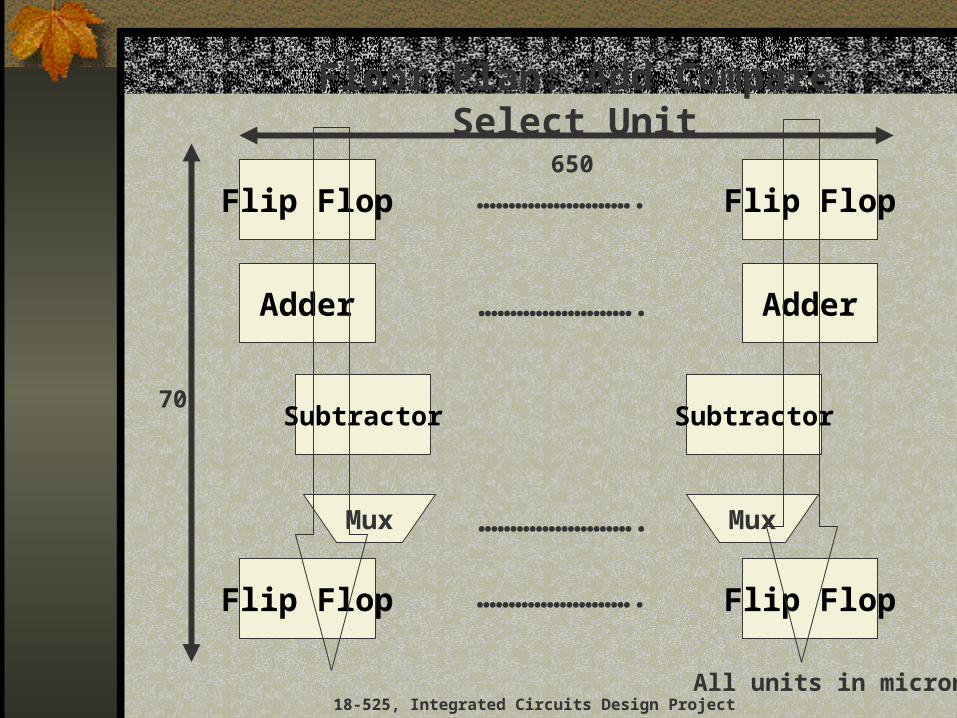
Floor Plan: Add Compare Select Unit
18-525, Integrated Circuits Design Project
Flip Flop ……………………. Flip Flop
Adder Adder…………………….
Subtractor Subtractor
Mux Mux
Flip Flop ……………………. Flip Flop
…………………….
70
650
All units in microns
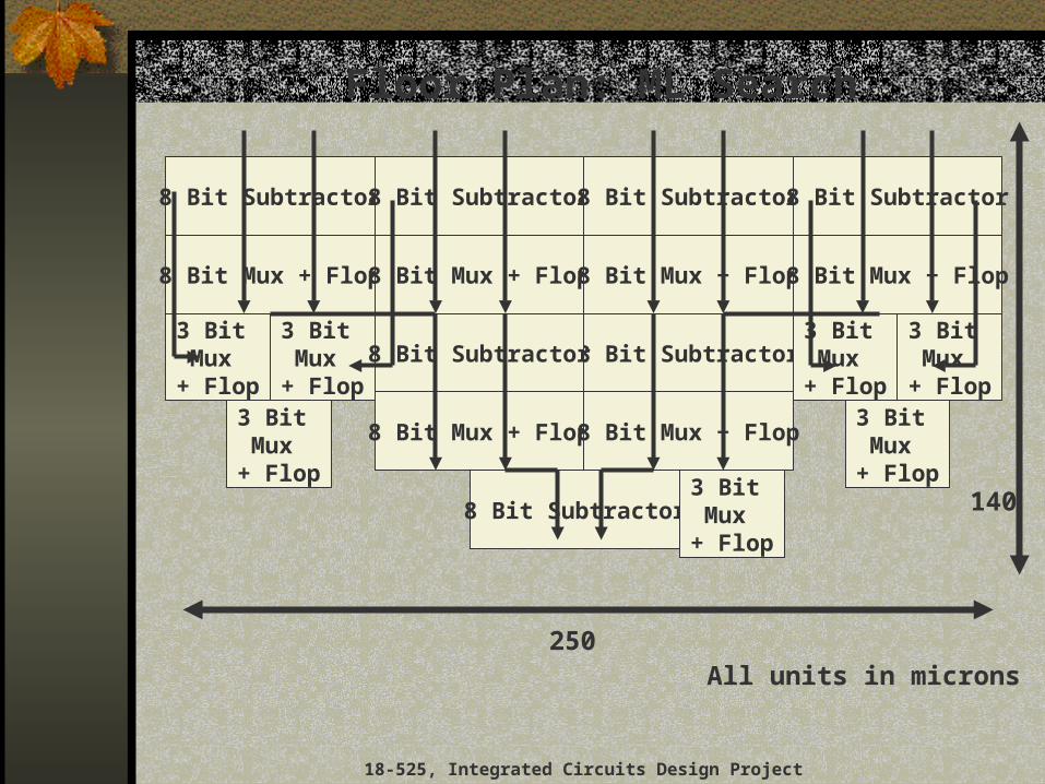
Floor Plan: ML Search
18-525, Integrated Circuits Design Project
8 Bit Subtractor 8 Bit Subtractor 8 Bit Subtractor 8 Bit Subtractor
8 Bit Mux + Flop 8 Bit Mux + Flop 8 Bit Mux + Flop 8 Bit Mux + Flop
8 Bit Subtractor
8 Bit Subtractor3 Bit Mux
+ Flop
3 Bit Mux
+ Flop
3 Bit Mux
+ Flop
3 Bit Mux
+ Flop3 Bit Mux
+ Flop
3 Bit Mux
+ Flop
8 Bit Subtractor
8 Bit Mux + Flop 8 Bit Mux + Flop
3 Bit Mux
+ Flop
250
140
All units in microns
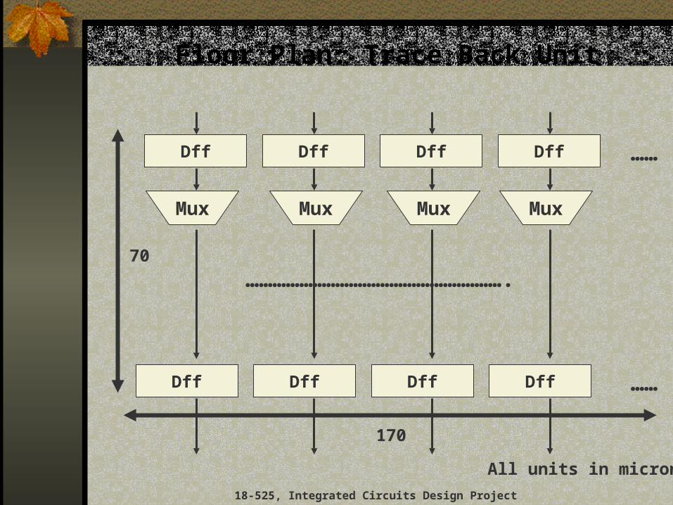
Floor Plan: Trace Back Unit
18-525, Integrated Circuits Design Project
Mux Mux Mux Mux
Dff Dff Dff Dff
……Dff Dff Dff Dff
………………………………………………….
……
170
70
All units in microns
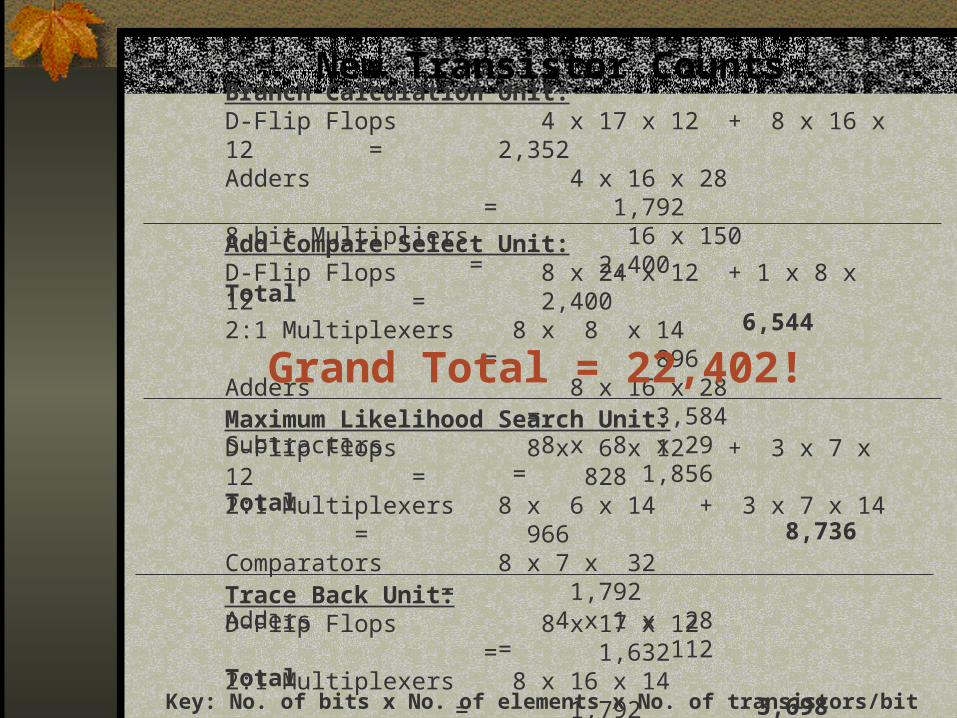
New Transistor Counts
Trace Back Unit:D-Flip Flops 8 x 17 x 12 = 1,632 2:1 Multiplexers 8 x 16 x 14 = 1,792Total 3,424
Branch Calculation Unit:D-Flip Flops 4 x 17 x 12 + 8 x 16 x 12 = 2,352Adders 4 x 16 x 28 = 1,7928 bit Multipliers 16 x 150 = 2,400Total 6,544
Add Compare Select Unit:D-Flip Flops 8 x 24 x 12 + 1 x 8 x 12 = 2,400 2:1 Multiplexers 8 x 8 x 14 = 896Adders 8 x 16 x 28 = 3,584Subtracters 8 x 8 x 29 = 1,856Total 8,736Maximum Likelihood Search Unit:D-Flip Flops 8 x 6 x 12 + 3 x 7 x 12 = 8282:1 Multiplexers 8 x 6 x 14 + 3 x 7 x 14 = 966Comparators 8 x 7 x 32 = 1,792Adders 4 x 1 x 28 = 112 Total 3,698
Grand Total = 22,402!
Key: No. of bits x No. of elements x No. of transistors/bit
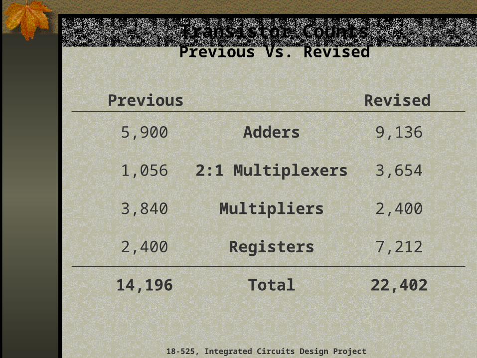
Transistor CountsPrevious Vs. Revised
18-525, Integrated Circuits Design Project
Adders
2:1 Multiplexers
Multipliers
Registers
Total
9,136
3,654
2,400
7,212
22,402
5,900
1,056
3,840
2,400
14,196
Previous Revised
18-525, Integrated Circuits Design Project
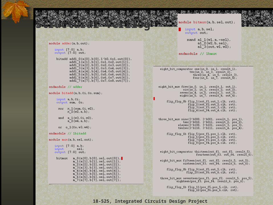
Structural Verilog
18-525, Integrated Circuits Design Project
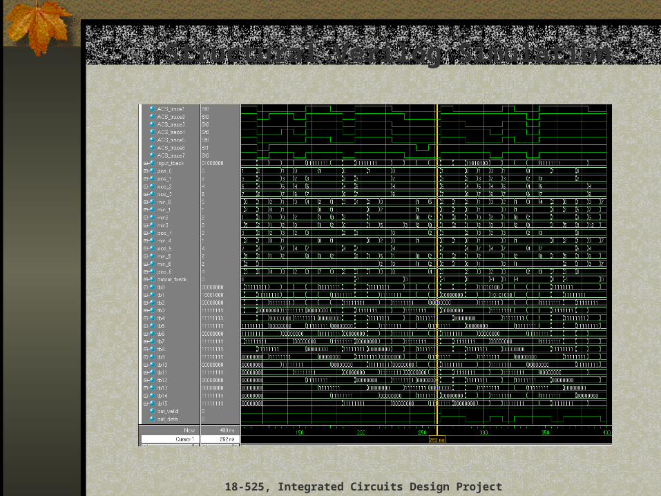
Structural Verilog Simulation
Questions?
18-525, Integrated Circuits Design Project