Embed Size (px)
Citation preview
This document is downloaded from DR‑NTU (https://dr.ntu.edu.sg)Nanyang Technological University, Singapore.
Resistive RAM endurance : array‑levelcharacterization and correction techniquestargeting deep learning applications
Grossi, Alessandro; Vianello, Elisa; Mohamed M. Sabry; Barlas, Marios; Grenouillet, Laurent;Coignus, Jean; Beigne, Edith; Wu, Tony; Le, Binh Q; Wootters, Mary K.; Zambelli, Cristian;Nowak, Etienne; Mitra, Subhasish
2019
Grossi, A., Vianello, E., Mohamed M. Sabry, Barlas, M., Grenouillet, L., Coignus, J., ... Mitra, S.(2019). Resistive RAM endurance : array‑level characterization and correction techniquestargeting deep learning applications. IEEE Transactions on Electron Devices, 66(3),1281‑1288. doi:10.1109/ted.2019.2894387
https://hdl.handle.net/10356/143255
https://doi.org/10.1109/TED.2019.2894387
© 2019 IEEE. Personal use of this material is permitted. Permission from IEEE must beobtained for all other uses, in any current or future media, includingreprinting/republishing this material for advertising or promotional purposes, creating newcollective works, for resale or redistribution to servers or lists, or reuse of any copyrightedcomponent of this work in other works. The published version is available at:https://doi.org/10.1109/TED.2019.2894387.
Downloaded on 18 Mar 2022 01:55:02 SGT
First Author et al.: Title
1
Abstract— Limited endurance of Resistive RAM (RRAM)
is a major challenge for future computing systems. Using thorough endurance tests that incorporate fine-grained read operations at the array level, we quantify for the first time temporary write failures (TWFs) caused by intrinsic RRAM cycle-to-cycle and cell-to-cell variations. We also quantify permanent write failures (PWFs) caused by irreversible breakdown/dissolution of the conductive filament. We show how technology-, RRAM programming- and system resilience-level solutions can be effectively combined to design new generations of energy-efficient computing systems that can successfully run deep learning (and other machine learning) applications despite TWFs and PWFs. We analyze corresponding system lifetimes and TWF BER.
Index Terms— RRAM, HfO2, variability, characterization, reliability, performance, deep learning
I. Introduction esistive RAM (RRAM [1]) is a non-volatile memory technology with a Metal-Insulator-Metal (MIM) stack
structure. RRAM stores data through the formation (set) and destruction (reset) of a conductive filament (CF) in the oxide insulator layer—a set operation switches the RRAM cell to a low-resistance state (LRS) while a reset operation switches the RRAM cell back to a high-resistance state (HRS) [2]. RRAM can provide massive on-chip data storage with low-voltage and low-latency accessibility and can be integrated using monolithic 3D integration. Thus, RRAM enables massive improvements in energy and execution time, especially for data-intensive applications such as deep learning [3, 4]. Despite major progress in RRAM technology [5], understanding variations in RRAM and the corresponding
We acknowledge the support of DARPA, NSF-SRC/NRI/GRC E2CDA, STARnet SONIC, NSF, member companies of the Stanford SystemX Alliance, and the NTU start-up grant.
A. Grossi, E. Vianello, M. Barlas, L. Grenouillet, J. Coignus, E. Beigne and E. Nowak are with CEA-Leti, Minatec Campus, Grenoble, France.
M. M. Sabry is with Nanyang Technological University, Singapore. T. Wu, B. Q. Le, M. K. Wootters and S. Mitra are with Dept. of EE,
Dept. of CS, Stanford SystemX Alliance, Stanford University, USA. C. Zambelli is with Dipartimento di Ingegneria, Universita degli Studi
di` Ferrara, Via Saragat 1, Ferrara, Italy.
system-level impact are open challenges that must be overcome.
One key challenge is the limited endurance of RRAM cells [6]. Endurance is usually defined as the number of set-reset operations (i.e., endurance cycles) after which the cell experiences a permanent-write failure (PWF, cell is stuck at HRS or LRS [6]). Several papers [6–11] have demonstrated up to 106 endurance cycles at the array level (Table I). RRAM also exhibits temporary-write failures (TWFs), which were previously demonstrated at a single-cell level [7].
In this paper, we characterize permanent and temporary write failures of RRAM arrays. We investigate the impact of RRAM endurance and TWF at the system level and overcome such RRAM failures by combining technology, RRAM programming, and system resilience techniques. Collectively, these techniques achieve a minimum of 4.5 years lifetime for deep learning applications (Section V).
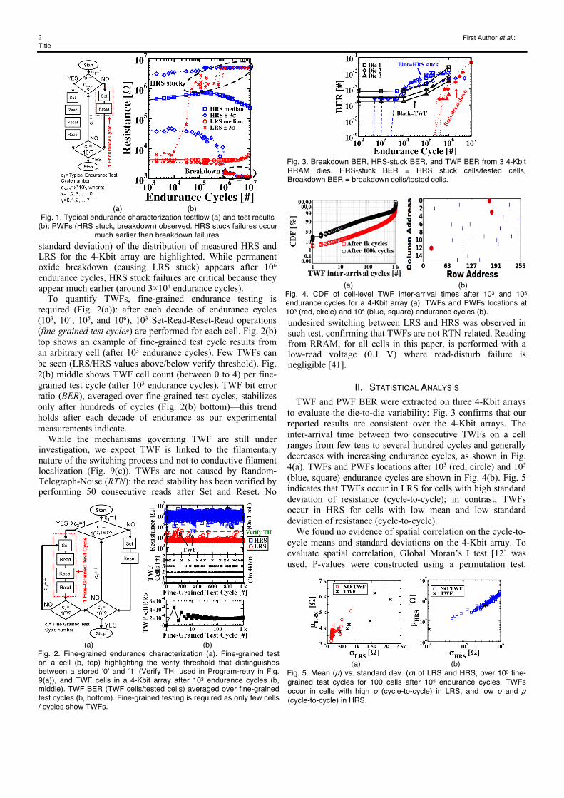
When an RRAM cell is in HRS, the read current is on the order of nA, resulting in long read time (100× longer than writes [7]) to measure the cell’s resistance value. Therefore, typical endurance tests (to quantify PWFs) contain only a few read operations per decade of endurance cycles (Table I). Fig. 1 reports a typical endurance test flow and corresponding results from a 4-Kbit array. The RRAM technology (300 nm diameter, TiN/HfO2/Ti/TiN) is monolithically integrated on top of 130 nm silicon CMOS process [7]. PWFs at 3σ (3× the
Alessandro Grossi, Elisa Vianello, Member, IEEE, Mohamed M. Sabry, Member, IEEE, Marios Barlas, Laurent Grenouillet, Jean Coignus, Edith Beigne, Tony Wu, Binh Q. Le, Mary
K. Wootters, Member, IEEE, Cristian Zambelli Member, IEEE, Etienne Nowak, and Subhasish Mitra, Fellow, IEEE
Resistive RAM Endurance: Array-level Characterization and Correction Techniques
Targeting Deep Learning Applications
R
TABLE I STATE OF THE ART OF RRAM ARRAYS ENDURANCE TESTING. ENDURANCE
WAS EVALUATED ON A LIMITED NUMBER OF CELLS WITH LOW READING GRANULARITY. TWFS WERE NOT STUDIED BY PREVIOUS PAPERS AT THE
ARRAY LEVEL. Ref. Array
size Tested cells
Read granularity
Endurance cycles
Failure investigated
[6] Few cells
Few cells
3 /decade of endurance cycles
106 HRS stuck, BD
[7] 4 Kbit 256 3 /decade 106 - [8] 16
Mbit 1 Mbit 1 /decade 106 -
[9] 2 Mbit
- 2 105 -
[10] 1 Mbit
1 Kbit 3 /decade 106 -
[11] 1 Mbit
1 Kbit 1 /decade 106 -
Ours 4 Kbit 4 Kbit ×3
1000 /decade 107 HRS stuck, BD, TWF
First Author et al.: Title
2
standard deviation) of the distribution of measured HRS and LRS for the 4-Kbit array are highlighted. While permanent oxide breakdown (causing LRS stuck) appears after 106 endurance cycles, HRS stuck failures are critical because they appear much earlier (around 3×10⁴ endurance cycles).
To quantify TWFs, fine-grained endurance testing is required (Fig. 2(a)): after each decade of endurance cycles (103, 104, 105, and 106), 103 Set-Read-Reset-Read operations (fine-grained test cycles) are performed for each cell. Fig. 2(b) top shows an example of fine-grained test cycle results from an arbitrary cell (after 103 endurance cycles). Few TWFs can be seen (LRS/HRS values above/below verify threshold). Fig. 2(b) middle shows TWF cell count (between 0 to 4) per fine-grained test cycle (after 103 endurance cycles). TWF bit error ratio (BER), averaged over fine-grained test cycles, stabilizes only after hundreds of cycles (Fig. 2(b) bottom)—this trend holds after each decade of endurance as our experimental measurements indicate.
While the mechanisms governing TWF are still under investigation, we expect TWF is linked to the filamentary nature of the switching process and not to conductive filament localization (Fig. 9(c)). TWFs are not caused by Random-Telegraph-Noise (RTN): the read stability has been verified by performing 50 consecutive reads after Set and Reset. No
undesired switching between LRS and HRS was observed in such test, confirming that TWFs are not RTN-related. Reading from RRAM, for all cells in this paper, is performed with a low-read voltage (0.1 V) where read-disturb failure is negligible [41].
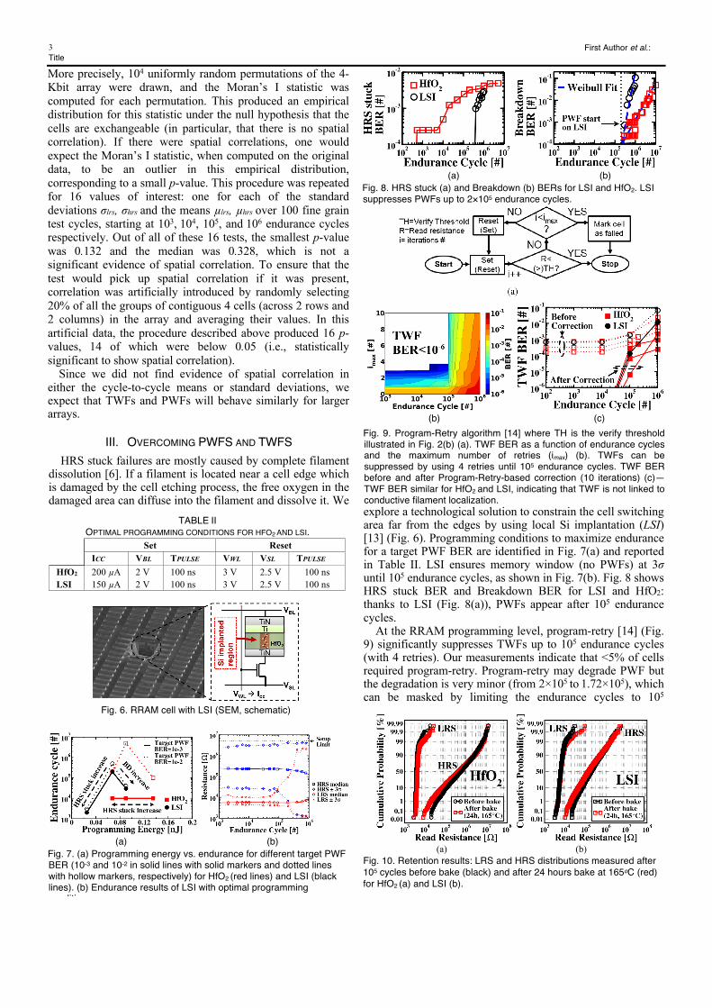
II. STATISTICAL ANALYSIS TWF and PWF BER were extracted on three 4-Kbit arrays
to evaluate the die-to-die variability: Fig. 3 confirms that our reported results are consistent over the 4-Kbit arrays. The inter-arrival time between two consecutive TWFs on a cell ranges from few tens to several hundred cycles and generally decreases with increasing endurance cycles, as shown in Fig. 4(a). TWFs and PWFs locations after 103 (red, circle) and 105 (blue, square) endurance cycles are shown in Fig. 4(b). Fig. 5 indicates that TWFs occur in LRS for cells with high standard deviation of resistance (cycle-to-cycle); in contrast, TWFs occur in HRS for cells with low mean and low standard deviation of resistance (cycle-to-cycle).
We found no evidence of spatial correlation on the cycle-to-cycle means and standard deviations on the 4-Kbit array. To evaluate spatial correlation, Global Moran’s I test [12] was used. P-values were constructed using a permutation test.
(a) (b)
Fig. 1. Typical endurance characterization testflow (a) and test results (b): PWFs (HRS stuck, breakdown) observed. HRS stuck failures occur
much earlier than breakdown failures.
(a) (b)
Fig. 4. CDF of cell-level TWF inter-arrival times after 103 and 105 endurance cycles for a 4-Kbit array (a). TWFs and PWFs locations at 103 (red, circle) and 105 (blue, square) endurance cycles (b).
Fig. 3. Breakdown BER, HRS-stuck BER, and TWF BER from 3 4-Kbit RRAM dies. HRS-stuck BER = HRS stuck cells/tested cells, Breakdown BER = breakdown cells/tested cells.
(a) (b) Fig. 2. Fine-grained endurance characterization (a). Fine-grained test on a cell (b, top) highlighting the verify threshold that distinguishes between a stored ‘0’ and ‘1’ (Verify TH, used in Program-retry in Fig. 9(a)), and TWF cells in a 4-Kbit array after 103 endurance cycles (b, middle). TWF BER (TWF cells/tested cells) averaged over fine-grained test cycles (b, bottom). Fine-grained testing is required as only few cells / cycles show TWFs.
(a) (b) Fig. 5. Mean (µ) vs. standard dev. (σ) of LRS and HRS, over 103 fine-grained test cycles for 100 cells after 105 endurance cycles. TWFs occur in cells with high σ (cycle-to-cycle) in LRS, and low σ and µ (cycle-to-cycle) in HRS.
First Author et al.: Title
3
More precisely, 104 uniformly random permutations of the 4-Kbit array were drawn, and the Moran’s I statistic was computed for each permutation. This produced an empirical distribution for this statistic under the null hypothesis that the cells are exchangeable (in particular, that there is no spatial correlation). If there were spatial correlations, one would expect the Moran’s I statistic, when computed on the original data, to be an outlier in this empirical distribution, corresponding to a small p-value. This procedure was repeated for 16 values of interest: one for each of the standard deviations σlrs, σhrs and the means µlrs, µhrs over 100 fine grain test cycles, starting at 103, 104, 105, and 106 endurance cycles respectively. Out of all of these 16 tests, the smallest p-value was 0.132 and the median was 0.328, which is not a significant evidence of spatial correlation. To ensure that the test would pick up spatial correlation if it was present, correlation was artificially introduced by randomly selecting 20% of all the groups of contiguous 4 cells (across 2 rows and 2 columns) in the array and averaging their values. In this artificial data, the procedure described above produced 16 p-values, 14 of which were below 0.05 (i.e., statistically significant to show spatial correlation).
Since we did not find evidence of spatial correlation in either the cycle-to-cycle means or standard deviations, we expect that TWFs and PWFs will behave similarly for larger arrays.
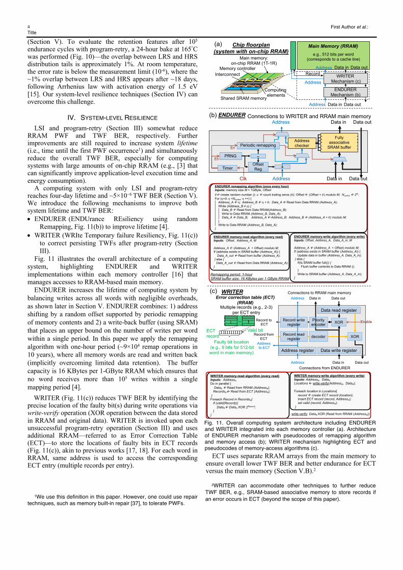
III. OVERCOMING PWFS AND TWFS HRS stuck failures are mostly caused by complete filament
dissolution [6]. If a filament is located near a cell edge which is damaged by the cell etching process, the free oxygen in the damaged area can diffuse into the filament and dissolve it. We
explore a technological solution to constrain the cell switching area far from the edges by using local Si implantation (LSI) [13] (Fig. 6). Programming conditions to maximize endurance for a target PWF BER are identified in Fig. 7(a) and reported in Table II. LSI ensures memory window (no PWFs) at 3σ until 105 endurance cycles, as shown in Fig. 7(b). Fig. 8 shows HRS stuck BER and Breakdown BER for LSI and HfO2: thanks to LSI (Fig. 8(a)), PWFs appear after 105 endurance cycles.
At the RRAM programming level, program-retry [14] (Fig. 9) significantly suppresses TWFs up to 105 endurance cycles (with 4 retries). Our measurements indicate that <5% of cells required program-retry. Program-retry may degrade PWF but the degradation is very minor (from 2×10⁵ to 1.72×10⁵), which can be masked by limiting the endurance cycles to 105
Fig. 6. RRAM cell with LSI (SEM, schematic)
TABLE II OPTIMAL PROGRAMMING CONDITIONS FOR HFO2 AND LSI.
Set Reset ICC VBL TPULSE VWL VSL TPULSE
HfO2 200 µA 2 V 100 ns 3 V 2.5 V 100 ns LSI 150 µA 2 V 100 ns 3 V 2.5 V 100 ns
(a) (b) Fig. 7. (a) Programming energy vs. endurance for different target PWF BER (10-3 and 10-2 in solid lines with solid markers and dotted lines with hollow markers, respectively) for HfO2 (red lines) and LSI (black lines). (b) Endurance results of LSI with optimal programming conditions.
(a) (b)
Fig. 8. HRS stuck (a) and Breakdown (b) BERs for LSI and HfO2. LSI suppresses PWFs up to 2×10⁵ endurance cycles.
(b) (c)
Fig. 9. Program-Retry algorithm [14] where TH is the verify threshold illustrated in Fig. 2(b) (a). TWF BER as a function of endurance cycles and the maximum number of retries (imax) (b). TWFs can be suppressed by using 4 retries until 105 endurance cycles. TWF BER before and after Program-Retry-based correction (10 iterations) (c)—TWF BER similar for HfO2 and LSI, indicating that TWF is not linked to conductive filament localization.
(a) (b) Fig. 10. Retention results: LRS and HRS distributions measured after 105 cycles before bake (black) and after 24 hours bake at 165oC (red) for HfO2 (a) and LSI (b).
First Author et al.: Title
4
(Section V). To evaluate the retention features after 105 endurance cycles with program-retry, a 24-hour bake at 165°C was performed (Fig. 10)—the overlap between LRS and HRS distribution tails is approximately 1%. At room temperature, the error rate is below the measurement limit (10-6), where the ~1% overlap between LRS and HRS appears after ~18 days, following Arrhenius law with activation energy of 1.5 eV [15]. Our system-level resilience techniques (Section IV) can overcome this challenge.
IV. SYSTEM-LEVEL RESILIENCE LSI and program-retry (Section III) somewhat reduce
RRAM PWF and TWF BER, respectively. Further improvements are still required to increase system lifetime (i.e., time until the first PWF occurrence1) and simultaneously reduce the overall TWF BER, especially for computing systems with large amounts of on-chip RRAM (e.g., [3] that can significantly improve application-level execution time and energy consumption).
A computing system with only LSI and program-retry reaches four-day lifetime and ~5×10⁻⁶ TWF BER (Section V). We introduce the following mechanisms to improve both system lifetime and TWF BER: • ENDURER (ENDUrance REsiliency using random
Remapping, Fig. 11(b)) to improve lifetime [4]. • WRITER (WRIte Temporary failure Resiliency, Fig. 11(c))
to correct persisting TWFs after program-retry (Section III).
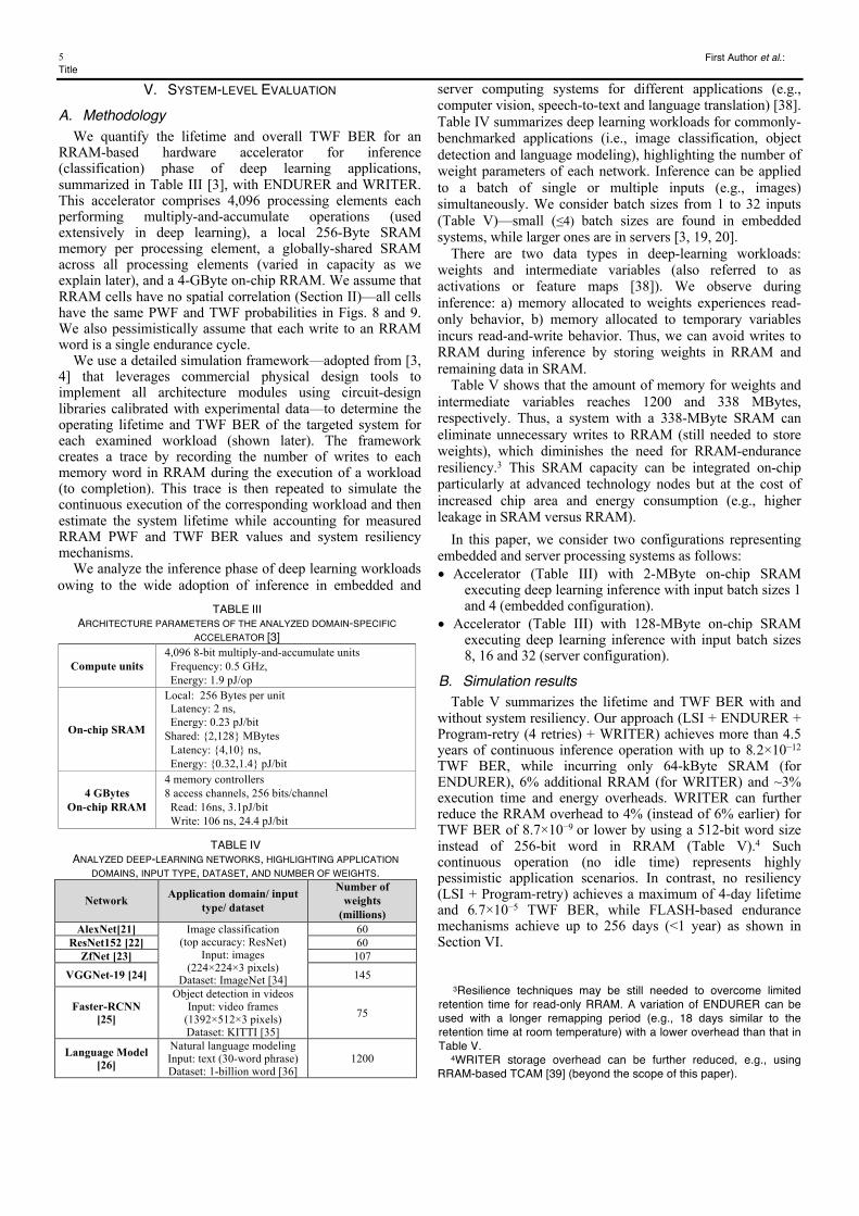
Fig. 11 illustrates the overall architecture of a computing system, highlighting ENDURER and WRITER implementations within each memory controller [16] that manages accesses to RRAM-based main memory.
ENDURER increases the lifetime of computing system by balancing writes across all words with negligible overheads, as shown later in Section V. ENDURER combines: 1) address shifting by a random offset supported by periodic remapping of memory contents and 2) a write-back buffer (using SRAM) that places an upper bound on the number of writes per word within a single period. In this paper we apply the remapping algorithm with one-hour period (~9×10⁴ remap operations in 10 years), where all memory words are read and written back (implicitly overcoming limited data retention). The buffer capacity is 16 KBytes per 1-GByte RRAM which ensures that no word receives more than 105 writes within a single mapping period [4].
WRITER (Fig. 11(c)) reduces TWF BER by identifying the precise location of the faulty bit(s) during write operations via write-verify operation (XOR operation between the data stored in RRAM and original data). WRITER is invoked upon each unsuccessful program-retry operation (Section III) and uses additional RRAM—referred to as Error Correction Table (ECT)—to store the locations of faulty bits in ECT records (Fig. 11(c)), akin to previous works [17, 18]. For each word in RRAM, same address is used to access the corresponding ECT entry (multiple records per entry).
1We use this definition in this paper. However, one could use repair
techniques, such as memory built-in repair [37], to tolerate PWFs.
ECT uses separate RRAM arrays from the main memory to ensure overall lower TWF BER and better endurance for ECT versus the main memory (Section V.B).2
2WRITER can accommodate other techniques to further reduce TWF BER, e.g., SRAM-based associative memory to store records if an error occurs in ECT (beyond the scope of this paper).
Fig. 11. Overall computing system architecture including ENDURER and WRITER integrated into each memory controller (a). Architecture of ENDURER mechanism with pseudocodes of remapping algorithm and memory access (b); WRITER mechanism highlighting ECT and pseudocodes of memory-access algorithms (c).
Data outData inAddress
Data inAddress
Computingelements
Shared SRAM memory
Memory controller
Main memory:on-chip RRAM (1T-1R)
Data out
Main Memory (RRAM)
Address
Record
Chip floorplan(system with on-chip RRAM)
WRITERMechanism (c)
Interconnect
e.g., 512 bits per word(corresponds to a cache line)
ENDURER Mechanism (b)
(a)
PRNG
Offset Reg
-
Periodic remapping
Data outData inAddressClk
En
En
Address checker
Timer
Fully associative
SRAM buffer
Connections to WRITER and RRAM main memoryData outData inAddress
(b) ENDURER
+
(c) WRITER
XOR
XORdecoder
Data out
Data out Data in Address
Address
Record toECT
Record fromECT
Addressto ECT
Data in
Data write registerAddress register
Data read register
Priority encoder
Record write register
Record read register
Faulty bit location(e.g., 9 bits for 512-bit word in main memory)
Error correction table (ECT) (RRAM)
ECT record
Valid bit
Multiple records (e.g., 2-3) per ECT entry
Enable
Connections from ENDURER
Connections to RRAM main memory
WRITER memory-read algorithm (every read)Inputs: AddressADo in parallel {
DataA ß Read from RRAM (AddressA);RecordsAß Read from ECT (AddressA);
}Foreach Record in RecordsA{
if (valid(Record)){DataAß DataA XOR 2Record;
}}
WRITER memory-write algorithm (every write)Inputs: AddressA, DataALocations ß write-verify(AddressA, DataA);
Foreach location in Locations{record ß create ECT record (location);Insert ECT record (record, AddressA);set valid (record, AddressA);
}
write-verify: DataA XOR (Read from RRAM (AddressA))
ENDURER remapping algorithm (once every hour)Inputs: memory size M = 1GByte, Offset!ß create random number (); " ß count trailing zeros (!); Offset ß (Offset + !) modulo M; Ncycles ß 2";For (#=0; # <Ncycles; # ++) {
Address_A ß #; Address_B ß # + !; Data_A ß Read from Data RRAM (Address_A);While (Address_B ≠ #) {
Data_B ß Read from Data RRAM(Address_B);Write to Data RRAM (Address_B, Data_A);Data_A ß Data_B; Address_A ß Address_B; Address_B ß (Address_A + !) modulo M;
}Write to Data RRAM (Address_B, Data_A);
}
ENDURER memory-read algorithm (every read)Inputs: Offset, Address_A, M
Address_A ß (Address_A + Offset) modulo M;If (address exists in SRAM buffer (Address_A)) {
Data_A_out ß Read from buffer (Address_A);} else {
Data_A_out ß Read from Data RRAM (Address_A);}
ENDURER memory-write algorithm (every write)Inputs: Offset, Address_A, Data_A_in, M
Address_A ß (Address_A + Offset) modulo M;If (address exists in SRAM buffer (Address_A)) {
Update data in buffer (Address_A, Data_A_in);} else {
If(is SRAM buffer full()) {Flush buffer contents to Data RRAM ();
}Write to SRAM buffer (Address_A, Data_A_in);
}Remapping period: 1-hourSRAM buffer size: 16 KBytes per 1 GByte RRAM
First Author et al.: Title
5
V. SYSTEM-LEVEL EVALUATION A. Methodology
We quantify the lifetime and overall TWF BER for an RRAM-based hardware accelerator for inference (classification) phase of deep learning applications, summarized in Table III [3], with ENDURER and WRITER. This accelerator comprises 4,096 processing elements each performing multiply-and-accumulate operations (used extensively in deep learning), a local 256-Byte SRAM memory per processing element, a globally-shared SRAM across all processing elements (varied in capacity as we explain later), and a 4-GByte on-chip RRAM. We assume that RRAM cells have no spatial correlation (Section II)—all cells have the same PWF and TWF probabilities in Figs. 8 and 9. We also pessimistically assume that each write to an RRAM word is a single endurance cycle.
We use a detailed simulation framework—adopted from [3, 4] that leverages commercial physical design tools to implement all architecture modules using circuit-design libraries calibrated with experimental data—to determine the operating lifetime and TWF BER of the targeted system for each examined workload (shown later). The framework creates a trace by recording the number of writes to each memory word in RRAM during the execution of a workload (to completion). This trace is then repeated to simulate the continuous execution of the corresponding workload and then estimate the system lifetime while accounting for measured RRAM PWF and TWF BER values and system resiliency mechanisms.
We analyze the inference phase of deep learning workloads owing to the wide adoption of inference in embedded and
server computing systems for different applications (e.g., computer vision, speech-to-text and language translation) [38]. Table IV summarizes deep learning workloads for commonly-benchmarked applications (i.e., image classification, object detection and language modeling), highlighting the number of weight parameters of each network. Inference can be applied to a batch of single or multiple inputs (e.g., images) simultaneously. We consider batch sizes from 1 to 32 inputs (Table V)—small (≤4) batch sizes are found in embedded systems, while larger ones are in servers [3, 19, 20].
There are two data types in deep-learning workloads: weights and intermediate variables (also referred to as activations or feature maps [38]). We observe during inference: a) memory allocated to weights experiences read-only behavior, b) memory allocated to temporary variables incurs read-and-write behavior. Thus, we can avoid writes to RRAM during inference by storing weights in RRAM and remaining data in SRAM.
Table V shows that the amount of memory for weights and intermediate variables reaches 1200 and 338 MBytes, respectively. Thus, a system with a 338-MByte SRAM can eliminate unnecessary writes to RRAM (still needed to store weights), which diminishes the need for RRAM-endurance resiliency.3 This SRAM capacity can be integrated on-chip particularly at advanced technology nodes but at the cost of increased chip area and energy consumption (e.g., higher leakage in SRAM versus RRAM).
In this paper, we consider two configurations representing embedded and server processing systems as follows: • Accelerator (Table III) with 2-MByte on-chip SRAM
executing deep learning inference with input batch sizes 1 and 4 (embedded configuration).
• Accelerator (Table III) with 128-MByte on-chip SRAM executing deep learning inference with input batch sizes 8, 16 and 32 (server configuration).
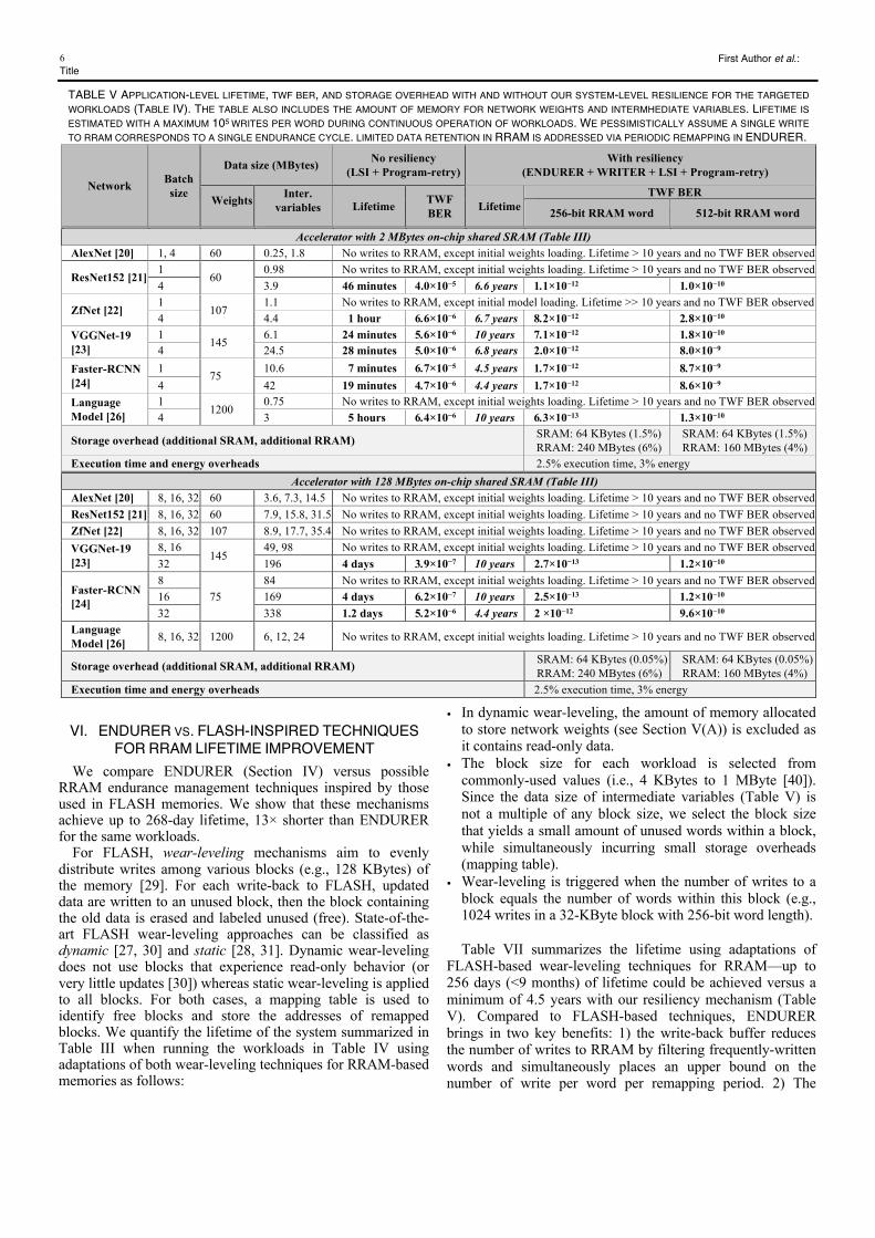
B. Simulation results Table V summarizes the lifetime and TWF BER with and
without system resiliency. Our approach (LSI + ENDURER + Program-retry (4 retries) + WRITER) achieves more than 4.5 years of continuous inference operation with up to 8.2×10⁻¹²
TWF BER, while incurring only 64-kByte SRAM (for ENDURER), 6% additional RRAM (for WRITER) and ~3% execution time and energy overheads. WRITER can further reduce the RRAM overhead to 4% (instead of 6% earlier) for TWF BER of 8.7×10⁻⁹ or lower by using a 512-bit word size instead of 256-bit word in RRAM (Table V).4 Such continuous operation (no idle time) represents highly pessimistic application scenarios. In contrast, no resiliency (LSI + Program-retry) achieves a maximum of 4-day lifetime and 6.7×10⁻⁵ TWF BER, while FLASH-based endurance mechanisms achieve up to 256 days (<1 year) as shown in Section VI.
3Resilience techniques may be still needed to overcome limited
retention time for read-only RRAM. A variation of ENDURER can be used with a longer remapping period (e.g., 18 days similar to the retention time at room temperature) with a lower overhead than that in Table V.
4WRITER storage overhead can be further reduced, e.g., using RRAM-based TCAM [39] (beyond the scope of this paper).
TABLE III ARCHITECTURE PARAMETERS OF THE ANALYZED DOMAIN-SPECIFIC
ACCELERATOR [3]
Compute units 4,096 8-bit multiply-and-accumulate units Frequency: 0.5 GHz, Energy: 1.9 pJ/op
On-chip SRAM
Local: 256 Bytes per unit Latency: 2 ns, Energy: 0.23 pJ/bit Shared: {2,128} MBytes Latency: {4,10} ns, Energy: {0.32,1.4} pJ/bit
4 GBytes On-chip RRAM
4 memory controllers 8 access channels, 256 bits/channel Read: 16ns, 3.1pJ/bit Write: 106 ns, 24.4 pJ/bit
TABLE IV
ANALYZED DEEP-LEARNING NETWORKS, HIGHLIGHTING APPLICATION DOMAINS, INPUT TYPE, DATASET, AND NUMBER OF WEIGHTS.
Network Application domain/ input type/ dataset
Number of weights
(millions) AlexNet[21] Image classification
(top accuracy: ResNet) Input: images
(224×224×3 pixels) Dataset: ImageNet [34]
60 ResNet152 [22] 60
ZfNet [23] 107 VGGNet-19 [24] 145
Faster-RCNN [25]
Object detection in videos Input: video frames
(1392×512×3 pixels) Dataset: KITTI [35]
75
Language Model [26]
Natural language modeling Input: text (30-word phrase) Dataset: 1-billion word [36]
1200
First Author et al.: Title
6
VI. ENDURER VS. FLASH-INSPIRED TECHNIQUES FOR RRAM LIFETIME IMPROVEMENT
We compare ENDURER (Section IV) versus possible RRAM endurance management techniques inspired by those used in FLASH memories. We show that these mechanisms achieve up to 268-day lifetime, 13× shorter than ENDURER for the same workloads.
For FLASH, wear-leveling mechanisms aim to evenly distribute writes among various blocks (e.g., 128 KBytes) of the memory [29]. For each write-back to FLASH, updated data are written to an unused block, then the block containing the old data is erased and labeled unused (free). State-of-the-art FLASH wear-leveling approaches can be classified as dynamic [27, 30] and static [28, 31]. Dynamic wear-leveling does not use blocks that experience read-only behavior (or very little updates [30]) whereas static wear-leveling is applied to all blocks. For both cases, a mapping table is used to identify free blocks and store the addresses of remapped blocks. We quantify the lifetime of the system summarized in Table III when running the workloads in Table IV using adaptations of both wear-leveling techniques for RRAM-based memories as follows:
• In dynamic wear-leveling, the amount of memory allocated to store network weights (see Section V(A)) is excluded as it contains read-only data.
• The block size for each workload is selected from commonly-used values (i.e., 4 KBytes to 1 MByte [40]). Since the data size of intermediate variables (Table V) is not a multiple of any block size, we select the block size that yields a small amount of unused words within a block, while simultaneously incurring small storage overheads (mapping table).
• Wear-leveling is triggered when the number of writes to a block equals the number of words within this block (e.g., 1024 writes in a 32-KByte block with 256-bit word length). Table VII summarizes the lifetime using adaptations of
FLASH-based wear-leveling techniques for RRAM—up to 256 days (<9 months) of lifetime could be achieved versus a minimum of 4.5 years with our resiliency mechanism (Table V). Compared to FLASH-based techniques, ENDURER brings in two key benefits: 1) the write-back buffer reduces the number of writes to RRAM by filtering frequently-written words and simultaneously places an upper bound on the number of write per word per remapping period. 2) The
TABLE V APPLICATION-LEVEL LIFETIME, TWF BER, AND STORAGE OVERHEAD WITH AND WITHOUT OUR SYSTEM-LEVEL RESILIENCE FOR THE TARGETED WORKLOADS (TABLE IV). THE TABLE ALSO INCLUDES THE AMOUNT OF MEMORY FOR NETWORK WEIGHTS AND INTERMHEDIATE VARIABLES. LIFETIME IS ESTIMATED WITH A MAXIMUM 105 WRITES PER WORD DURING CONTINUOUS OPERATION OF WORKLOADS. WE PESSIMISTICALLY ASSUME A SINGLE WRITE TO RRAM CORRESPONDS TO A SINGLE ENDURANCE CYCLE. LIMITED DATA RETENTION IN RRAM IS ADDRESSED VIA PERIODIC REMAPPING IN ENDURER.
Network Batch size
Data size (MBytes) No resiliency (LSI + Program-retry)
With resiliency (ENDURER + WRITER + LSI + Program-retry)
Weights Inter. variables Lifetime TWF
BER Lifetime TWF BER
256-bit RRAM word 512-bit RRAM word
Accelerator with 2 MBytes on-chip shared SRAM (Table III) AlexNet [20] 1, 4 60 0.25, 1.8 No writes to RRAM, except initial weights loading. Lifetime > 10 years and no TWF BER observed
ResNet152 [21] 1
60 0.98 No writes to RRAM, except initial weights loading. Lifetime > 10 years and no TWF BER observed
4 3.9 46 minutes 4.0×10⁻⁵ 6.6 years 1.1×10⁻¹² 1.0×10⁻¹⁰
ZfNet [22] 1
107 1.1 No writes to RRAM, except initial model loading. Lifetime >> 10 years and no TWF BER observed
4 4.4 1 hour 6.6×10⁻⁶ 6.7 years 8.2×10⁻¹² 2.8×10⁻¹⁰ VGGNet-19 [23]
1 145
6.1 24 minutes 5.6×10⁻⁶ 10 years 7.1×10⁻¹² 1.8×10⁻¹⁰ 4 24.5 28 minutes 5.0×10⁻⁶ 6.8 years 2.0×10⁻¹² 8.0×10⁻⁹
Faster-RCNN [24]
1 75
10.6 7 minutes 6.7×10⁻⁵ 4.5 years 1.7×10⁻¹² 8.7×10⁻⁹ 4 42 19 minutes 4.7×10⁻⁶ 4.4 years 1.7×10⁻¹² 8.6×10⁻⁹
Language Model [26]
1 1200
0.75 No writes to RRAM, except initial weights loading. Lifetime > 10 years and no TWF BER observed 4 3 5 hours 6.4×10⁻⁶ 10 years 6.3×10⁻¹³ 1.3×10⁻¹⁰
Storage overhead (additional SRAM, additional RRAM) SRAM: 64 KBytes (1.5%) RRAM: 240 MBytes (6%)
SRAM: 64 KBytes (1.5%) RRAM: 160 MBytes (4%)
Execution time and energy overheads 2.5% execution time, 3% energy Accelerator with 128 MBytes on-chip shared SRAM (Table III)
AlexNet [20] 8, 16, 32 60 3.6, 7.3, 14.5 No writes to RRAM, except initial weights loading. Lifetime > 10 years and no TWF BER observed ResNet152 [21] 8, 16, 32 60 7.9, 15.8, 31.5 No writes to RRAM, except initial weights loading. Lifetime > 10 years and no TWF BER observed ZfNet [22] 8, 16, 32 107 8.9, 17.7, 35.4 No writes to RRAM, except initial weights loading. Lifetime > 10 years and no TWF BER observed VGGNet-19 [23]
8, 16 145
49, 98 No writes to RRAM, except initial weights loading. Lifetime > 10 years and no TWF BER observed 32 196 4 days 3.9×10⁻⁷ 10 years 2.7×10⁻¹³ 1.2×10⁻¹⁰
Faster-RCNN [24]
8 75
84 No writes to RRAM, except initial weights loading. Lifetime > 10 years and no TWF BER observed 16 169 4 days 6.2×10⁻⁷ 10 years 2.5×10⁻¹³ 1.2×10⁻¹⁰ 32 338 1.2 days 5.2×10⁻⁶ 4.4 years 2 ×10⁻¹² 9.6×10⁻¹⁰
Language Model [26] 8, 16, 32 1200 6, 12, 24 No writes to RRAM, except initial weights loading. Lifetime > 10 years and no TWF BER observed
Storage overhead (additional SRAM, additional RRAM) SRAM: 64 KBytes (0.05%) RRAM: 240 MBytes (6%)
SRAM: 64 KBytes (0.05%) RRAM: 160 MBytes (4%)
Execution time and energy overheads 2.5% execution time, 3% energy
First Author et al.: Title
7
random remapping is applied at the word level causing all RRAM words to experience similar number of writes. On the contrary, FLASH-based techniques do not distribute the number of writes within a block which in turn reduces the lifetime. Using a smaller block size (e.g., one word per block) incurs significant storage overheads—up to 145 MBytes SRAM for a 4-GByte RRAM.
VII. CONCLUSIONS Overcoming endurance and temporary-failures challenges
are essential to use RRAM as a working on-chip memory. Our end-to-end approach to overcome such challenge includes extensive experimental characterization as well as effective combination of technology-, RRAM programming-, and system resilience-level solutions. This approach paves the path for deep learning on RRAM-based computing systems with long lifetime and reduced temporary bit-error rates.
REFERENCES [1] T. Werner et al., "Experimental demonstration of short and long term
synaptic plasticity using OxRAM multi k-bit arrays for reliable
detection in highly noisy input data," 2016 IEEE International Electron Devices Meeting (IEDM), San Francisco, CA, 2016, pp. 16.6.1-16.6.4. doi: 10.1109/IEDM.2016.7838433
[2] G. Bersuker, D. C. Gilmer, D. Veksler, P. Kirsch, L. Vandelli, A. Padovani, et al., “Metal oxide resistive memory switching mechanism based on conductive filament properties,” Journal of Applied Physics, vol. 110, no. 12, pp. 1–12, 2011. doi: 10.1063/1.3671565
[3] W. Hwang et al., "Special session paper 3D nanosystems enable embedded abundant-data computing," 2017 International Conference on Hardware/Software Codesign and System Synthesis (CODES+ISSS), Seoul, 2017, pp. 1-2. doi: 10.1145/3125502.3125531
[4] M. M. Sabry Aly et al., "The N3XT Approach to Energy-Efficient Abundant-Data Computing”, in Proceedings of the IEEE, (in press), 2019. doi: 10.1109/JPROC.2018.2882603
[5] L. Perniola et al., "Universal Signatures from Non-Universal Memories: Clues for the Future...," 2016 IEEE 8th International Memory Workshop (IMW), Paris, 2016, pp. 1-3. doi: 10.1109/IMW.2016.7495295
[6] Y. Y. Chen et al., “Balancing SET/RESET Pulse for Endurance in 1T1R Bipolar RRAM”. IEEE Transactions on Electron Devices. 59, 2012. 3243. 10.1109/TED.2012.2218607.
[7] A. Grossi et al., "Fundamental variability limits of filament-based RRAM," 2016 IEEE International Electron Devices Meeting (IEDM), San Francisco, CA, 2016, pp. 4.7.1-4.7.4. doi: 10.1109/IEDM.2016.7838348
[8] Z. Chen et al., "Performance Improvements by SL-Current Limiter and Novel Programming Methods on 16MB RRAM Chip," 2017 IEEE International Memory Workshop (IMW), Monterey, CA, 2017, pp. 1-4. doi: 10.1109/IMW.2017.7939097
[9] Y. Hayakawa et al., "Highly reliable TaOxReRAM with centralized filament for 28-nm embedded application," 2015 Symposium on VLSI Technology (VLSI Technology), Kyoto, 2015, pp. T14-T15. doi: 10.1109/VLSIT.2015.7223684
[10] A. Calderoni, S. Sills and N. Ramaswamy, "Performance comparison of O-based and Cu-based ReRAM for high-density applications," 2014 IEEE 6th International Memory Workshop (IMW), Taipei, 2014, pp. 1-4. doi: 10.1109/IMW.2014.6849351
[11] A. Mallik et al., "Design-technology co-optimization for OxRRAM-based synaptic processing unit," 2017 Symposium on VLSI Technology, Kyoto, 2017, pp. T178-T179. doi: 10.23919/VLSIT.2017.7998166.
[12] L. Anselin, Spatial Econometrics: Methods and Models. Springer Netherlands, 1988.
[13] M. Barlas et al., "Improvement of HfO2based RRAM array performances by local Si implantation," 2017 IEEE International Electron Devices Meeting (IEDM), San Francisco, CA, 2017, pp. 14.6.1-14.6.4. doi: 10.1109/IEDM.2017.8268392
[14] A. Belmonte, A. Fantini, A. Redolfi, M. Houssa, M. Jurczak and L. Goux, "Optimization of the write algorithm at low-current (10μA) in Cu/Al2O3-based conductive-bridge RAM," 2015 45th European Solid State Device Research Conference (ESSDERC), Graz, 2015, pp. 114-117. doi: 10.1109/ESSDERC.2015.7324726
[15] B. Traoré, P. Blaise, E. Vianello, H. Grampeix, S. Jeannot, L. Perniola, B. De Salvo, and Y. Nishi, “On the Origin of Low-Resistance State Retention Failure in HfO2-Based RRAM and Impact of Doping/Alloying”, in IEEE Trans. on Electron Devices, Vol. 62, no. 12, pp. 4029, 4036, 2015. DOI: 10.1109/TED.2015.2490545
[16] B. Jacob, S. Ng, and D. Wang, Memory systems: cache, DRAM, disk. Morgan Kaufmann, 2010.
[17] S. Schechter, G. H. Loh, K. Straus, and D. Burger, “Use ECP, not ECC, for hard failures in resistive memories”. ACM SIGARCH Computer Architecture News, 2009. 38. 141. 10.1145/1816038.1815980.
[18] M. K. Qureshi, "Pay-As-You-Go: Low-overhead hard-error correction for phase change memories," 2011 44th Annual IEEE/ACM International Symposium on Microarchitecture (MICRO), Porto Alegre, 2011, pp. 318-328.
[19] S. Han, X. Liu, H. Mao, J. Pu, A. Pedram, M. A. Horowitz, and W. J. Dally, “Eie: efficient inference engine on compressed deep neural network,” in Proc. ISCA, 2016. pp. 243–254. arXiv:1602.01528
[20] N. P. Jouppi, C. Young, N. Patil, D. Patterson, G. Agrawal, R. Bajwa, et al., “In-datacenter performance analysis of a tensor processing unit,” in Proc. ISCA, 2017, pp. 1–12. doi: 10.1145/3079856.3080246
[21] A. Krizhevsky, I. Sutskever, and G. E. Hinton, “ImageNet Classification with Deep Convolutional Neural Networks”. Neural Information Processing Systems, 2012. 25. 10.1145/3065386.
[22] K. He, X. Zhang, S. Ren and J. Sun, "Deep Residual Learning for Image Recognition," 2016 IEEE Conference on Computer Vision and Pattern Recognition (CVPR), Las Vegas, NV, 2016, pp. 770-778. doi: 10.1109/CVPR.2016.90
TABLE VI APPLICATION-LEVEL LIFETIME AND STORAGE OVERHEAD OF THE ANALYZED
FLASH-BASED WEAR-LEVELING MECHANISMS. LIFETIME IS ESTIMATED WITH A MAXIMUM 105 WRITES PER WORD. WE PESSIMISTICALLY ASSUME A SINGLE
WRITE TO RRAM CORRESPONDS TO A SINGLE ENDURANCE CYCLE.
Network Batch size
Adaptation of FLASH-based wear-leveling Block size (kByte)
Dynamic [27] Static [28]
Lifetime (days)
Storage overhd (KByte)
Lifetime (days)
Storage overhd (KByte)
Accelerator with 2 MBytes on-chip shared SRAM (Table III) AlexNet [21]
1,4 No writes to RRAM, except initial weights loading. Lifetime > 10 years
ResNet152 [22]
1 No writes to RRAM, except initial weights loading. Lifetime > 10 years
4 32 60 453 46 256 ZfNet [23] 1 No writes to RRAM, except initial weights loading.
Lifetime > 10 years 4 128 37 105 43 56
VGGNet-19 [24]
1 16 41 937 8 544 4 32 13 453 8 256
Faster-RCNN [25]
1 64 9 218 9 120 4 128 6 105 7 56
Language Model [26]
1 No writes to RRAM, except initial weights loading. Lifetime > 10 years
4 128 70 105 194 56 Accelerator with 128 MBytes on-chip shared SRAM (Table III)
AlexNet [21]
8, 16, 32
No writes to RRAM, except initial weights loading. Lifetime > 10 years
ResNet152 [22]
8, 16, 32
No writes to RRAM, except initial weights loading. Lifetime > 10 years
ZfNet [22] 8, 16, 32
No writes to RRAM, except initial weights loading. Lifetime > 10 years
ZfNet [23] 8, 16 No writes to RRAM, except initial weights loading. Lifetime > 10 years
32 128 115 105 114 56 VGGNet-19 [24] Faster-RCNN [25]
8 No writes to RRAM, except initial weights loading. Lifetime > 10 years
16 256 258 50 130 26 32 512 52 24 40 12
Language Model [25]
8, 16, 32
No writes to RRAM, except initial weights loading. Lifetime > 10 years
First Author et al.: Title
8
[23] M. D. Zeiler and R. Fergus, “Visualizing and understanding convolutional networks,” in European conference on computer vision. Springer, 2014, pp. 818–833. doi:
[24] K. Simonyan and A. Zisserman, “Very deep convolutional networks for large-scale image recognition,” arXiv preprint arXiv:1409.1556, 2014.
[25] S. Ren, K. He, R. Girshick, and J. Sun, “Faster r-cnn: Towards real-time object detection with region proposal networks,” in Advances in neural information processing systems, 2015, pp. 91–99. doi: 10.1109/TPAMI.2016.2577031
[26] R. Jozefowicz, O. Vinyals, M. Schuster, N. Shazeer, and Y. Wu, “Exploring the Limits of Language Modeling,” CoRR, vol. 1602.02410, 2016.
[27] Micron Technology Corp., Micron Tech. Appl. Note (TN-29-42), “Wearleveling techniques in nand flash devices,” 2008.
[28] Y. Chang, J. Hsieh and T. Kuo, "Endurance Enhancement of Flash-Memory Storage, Systems: An Efficient Static Wear Leveling Design," 2007 44th ACM/IEEE Design Automation Conference, San Diego, CA, 2007, pp. 212-217.
[29] Y.-H. Chang and L.-P. Chang, “Efficient wear leveling in NAND flash memory”. Springer Series in Advanced Microelectronics, 2018. 343-367. doi: 10.1007/978-981-13-0599-3_10.
[30] Numonyx., Numonyx Appl. note (AN1822)., “Wear leveling in nand flash memories.” 2008.
[31] Y. Gudeta, S. J. Kwon, E.-S. Cho, and T.-S. Chung, “Probability-based static wear-leveling algorithm for block and hybrid-mapping NAND flash memory”. Design Automation for Embedded Systems, 2012. 16. 10.1007/s10617-013-9108-3
[32] L.-P. Chang, and C.-D. Du, “Design and Implementation of an Efficient Wear-Leveling Algorithm for Solid-State-Disk Microcontrollers”. ACM Trans. Design Autom. Electr. Syst, 2009.. 15. 10.1145/1640457.1640463.
[33] R. Yamashita et al., "11.1 A 512Gb 3b/cell flash memory on 64-word-line-layer BiCS technology," 2017 IEEE International Solid-State Circuits Conference (ISSCC), San Francisco, CA, 2017, pp. 196-197. doi: 10.1109/ISSCC.2017.7870328
[34] J. Deng, W. Dong, R. Socher, L. Li, Kai Li and Li Fei-Fei, "ImageNet: A large-scale hierarchical image database," 2009 IEEE Conference on Computer Vision and Pattern Recognition, Miami, FL, 2009, pp. 248-255. doi: 10.1109/CVPR.2009.5206848
[35] A. Geiger, P. Lenz, C. Stiller, and R. Urtasun. “Vision Meets Robotics: The KITTI Dataset.” The International Journal of Robotics Research 32, no. 11 (September 2013): 1231–37. doi:10.1177/0278364913491297.
[36] C. Chelba et al. "One billion word benchmark for measuring progress in statistical language modeling." arXiv preprint arXiv:1312.3005 (2013). http://www.statmt.org/lm-benchmark/
[37] M. Nicolaidis, N. Achouri and L. Anghel, "A diversified memory built-in self-repair approach for nanotechnologies," 22nd IEEE VLSI Test Symposium, 2004. Proceedings., Napa Valley, CA, USA, 2004, pp. 313-318. doi: 10.1109/VTEST.2004.1299258
[38] Y. LeCun et al., “Deep Learning”, in Nature vol. 521, 2015. doi: 10.1038/nature14539
[39] A. Grossi et al., "Experimental Investigation of 4-kb RRAM Arrays Programming Conditions Suitable for TCAM," in IEEE Transactions on Very Large Scale Integration (VLSI) Systems. doi: 10.1109/TVLSI.2018.2805470
[40] J. Kim, J. M. Kim, S. H. Noh, S. L. Min and Y. Cho, "A space-efficient flash translation layer for CompactFlash systems," in IEEE Transactions on Consumer Electronics, vol. 48, no. 2, pp. 366-375, May 2002. doi: 10.1109/TCE.2002.10101.
[41] G. Sassine et al., “Sub-pJ Consumption and Short Latency Time in RRAM Arrays for High Endurance Applications”, in 2018 IEEE international Reliability Physica Symposiun (IRPS), 2018. DOI: 10.1109/IRPS.2018.8353675

![Resistive RAM embedded MCU - Panasonic s first sampling MCU with built-in Resistive RAM (ReRAM) Abstract Added value Application Smart meter ... EWme-ReRAM1.ppt [Kompatibilitätsmodus]](https://img.pdfslide.us/doc/110x75/5aaa87387f8b9a9a188e5792/resistive-ram-embedded-mcu-panasonic-s-first-sampling-mcu-with-built-in-resistive.jpg)