Embed Size (px)
Citation preview
CE 1911
Memory Overview
2 © tjCE 1911 – Spring 2017
Memory Overview
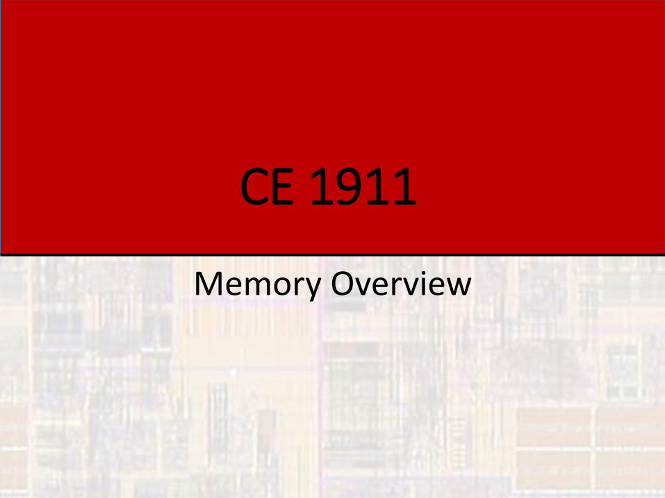
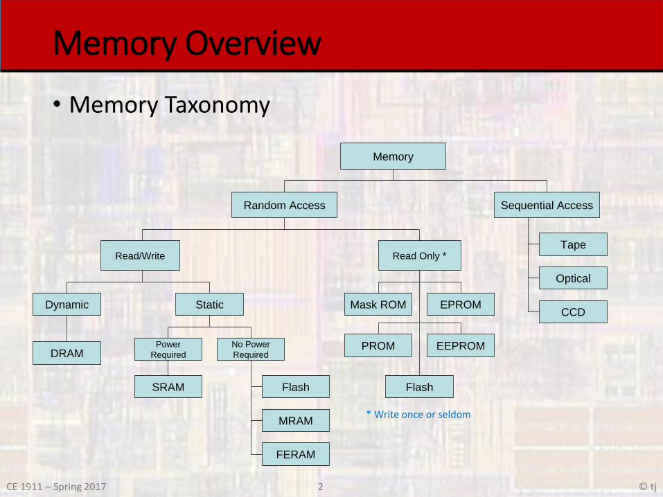
• Memory Taxonomy
Random Access
Read/Write Read Only *
Mask ROM
PROM
EPROM
EEPROM
Dynamic Static
Power
Required
No Power
Required
FlashSRAM Flash
MRAM
FERAM
DRAM
Sequential Access
Tape
Optical
CCD
Memory
* Write once or seldom
3 © tjCE 1911 – Spring 2017
Memory Overview
• Memory Taxonomy• Key Attributes• Sequential vs. Random Access
• Read only vs. Read/Write
• Static vs. Dynamic
• Volatile vs. non-Volatile
• Key Measures• Density
• Speed
• Power
• Cost / bit
4 © tjCE 1911 – Spring 2017
Memory Overview
• Memory Taxonomy
• Terminology WARNING
• b – bit
• B – Byte
• 1Mb can mean either 1,048,600 bits
or 1,000,000 bits
• 16Gb Flash drive when checked on your PC may read 14.9Gb
5 © tjCE 1911 – Spring 2017
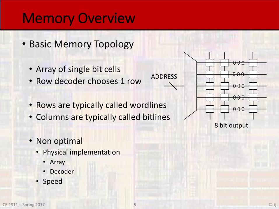
Memory Overview
• Basic Memory Topology
• Array of single bit cells
• Row decoder chooses 1 row
• Rows are typically called wordlines
• Columns are typically called bitlines
• Non optimal• Physical implementation• Array
• Decoder
• Speed
ADDRESS
8 bit output
6 © tjCE 1911 – Spring 2017
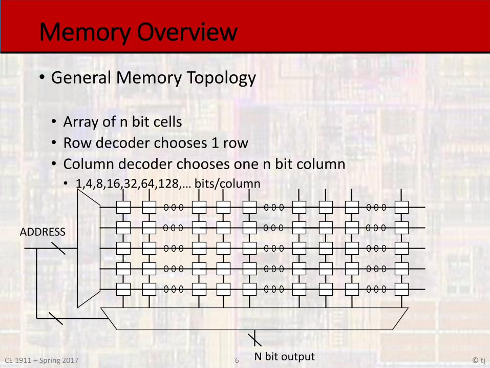
Memory Overview
• General Memory Topology
• Array of n bit cells
• Row decoder chooses 1 row
• Column decoder chooses one n bit column • 1,4,8,16,32,64,128,… bits/column
ADDRESS
N bit output
7 © tjCE 1911 – Spring 2017
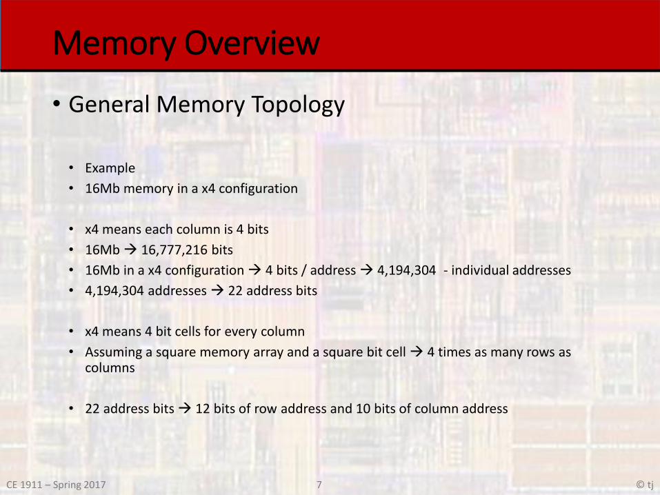
Memory Overview
• General Memory Topology
• Example
• 16Mb memory in a x4 configuration
• x4 means each column is 4 bits
• 16Mb 16,777,216 bits
• 16Mb in a x4 configuration 4 bits / address 4,194,304 - individual addresses
• 4,194,304 addresses 22 address bits
• x4 means 4 bit cells for every column
• Assuming a square memory array and a square bit cell 4 times as many rows as columns
• 22 address bits 12 bits of row address and 10 bits of column address
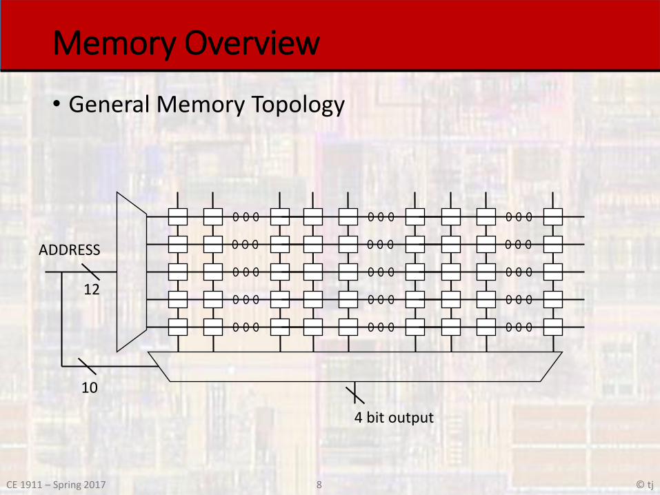
8 © tjCE 1911 – Spring 2017
Memory Overview
• General Memory Topology
ADDRESS
4 bit output
12
10
9 © tjCE 1911 – Spring 2017
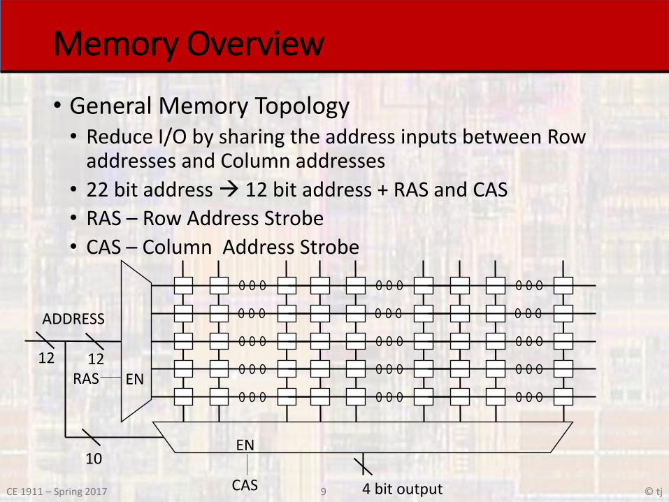
Memory Overview
• General Memory Topology• Reduce I/O by sharing the address inputs between Row
addresses and Column addresses
• 22 bit address 12 bit address + RAS and CAS
• RAS – Row Address Strobe
• CAS – Column Address Strobe
ADDRESS
4 bit output
12
10
EN
EN
RAS
CAS
12
10 © tjCE 1911 – Spring 2017
Memory Overview
Read Only Memory - ROM
11 © tjCE 1911 – Spring 2017
Memory Overview
• Read Only Memory - ROM• Key Attributes• Sequential vs. Random Access
• Read only vs. Read/Write
• Static vs. Dynamic
• Volatile vs. non-Volatile
• Key Measures• Density
• Speed
• Power
• Cost / bit
+
+
12 © tjCE 1911 – Spring 2017
Memory Overview
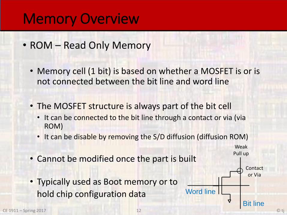
• ROM – Read Only Memory
• Memory cell (1 bit) is based on whether a MOSFET is or is not connected between the bit line and word line
• The MOSFET structure is always part of the bit cell• It can be connected to the bit line through a contact or via (via
ROM)
• It can be disable by removing the S/D diffusion (diffusion ROM)
• Cannot be modified once the part is built
• Typically used as Boot memory or to
hold chip configuration data Word line
Bit line
Contactor Via
WeakPull up
13 © tjCE 1911 – Spring 2017
Memory Overview
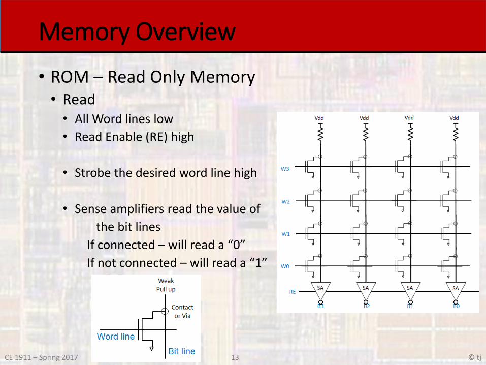
• ROM – Read Only Memory• Read• All Word lines low
• Read Enable (RE) high
• Strobe the desired word line high
• Sense amplifiers read the value of
the bit lines
If connected – will read a “0”
If not connected – will read a “1”
14 © tjCE 1911 – Spring 2017
Memory Overview
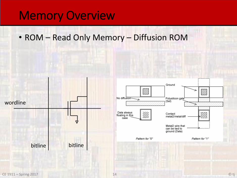
• ROM – Read Only Memory – Diffusion ROM
wordline
bitline bitline
15 © tjCE 1911 – Spring 2017
Memory Overview
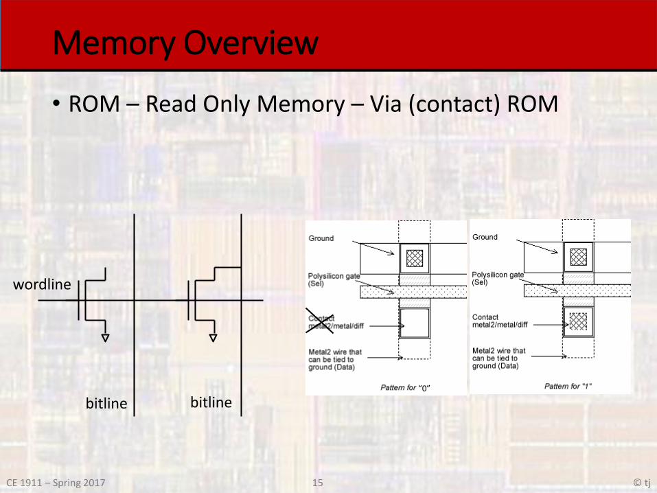
• ROM – Read Only Memory – Via (contact) ROM
“0”
wordline
bitline bitline
16 © tjCE 1911 – Spring 2017
Memory Overview
Static Random Access Memory - SRAM
17 © tjCE 1911 – Spring 2017
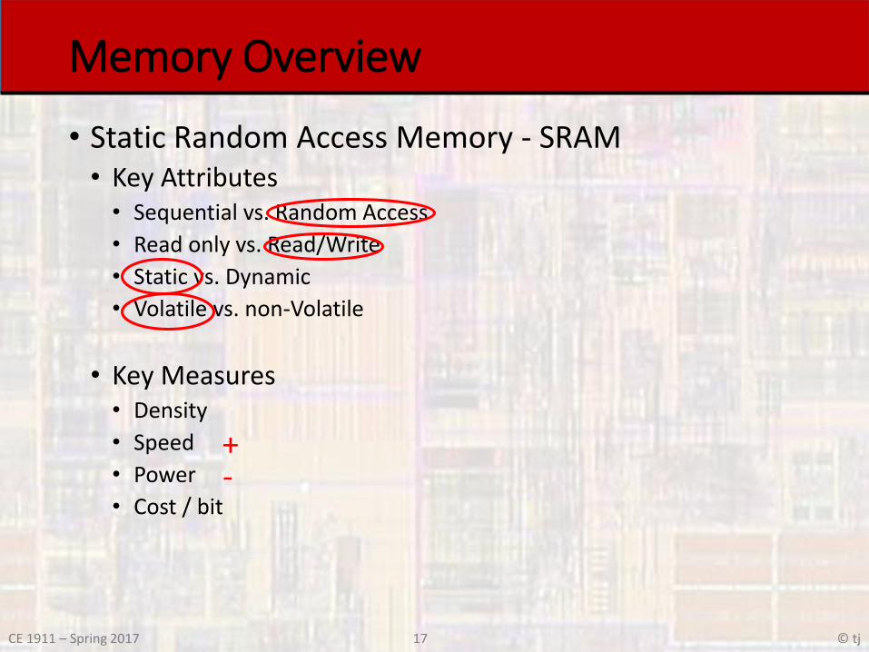
Memory Overview
• Static Random Access Memory - SRAM• Key Attributes• Sequential vs. Random Access
• Read only vs. Read/Write
• Static vs. Dynamic
• Volatile vs. non-Volatile
• Key Measures• Density
• Speed
• Power
• Cost / bit
+-
18 © tjCE 1911 – Spring 2017
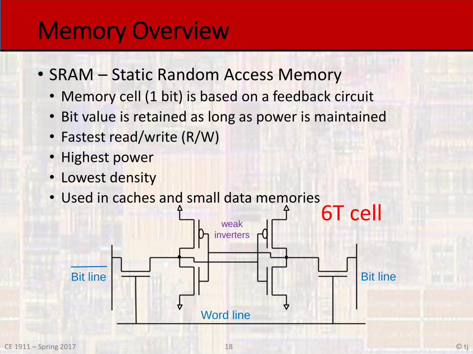
Memory Overview
• SRAM – Static Random Access Memory• Memory cell (1 bit) is based on a feedback circuit
• Bit value is retained as long as power is maintained
• Fastest read/write (R/W)
• Highest power
• Lowest density
• Used in caches and small data memories
Word line
Bit lineBit line
weak
inverters
6T cell
19 © tjCE 1911 – Spring 2017
Memory Overview
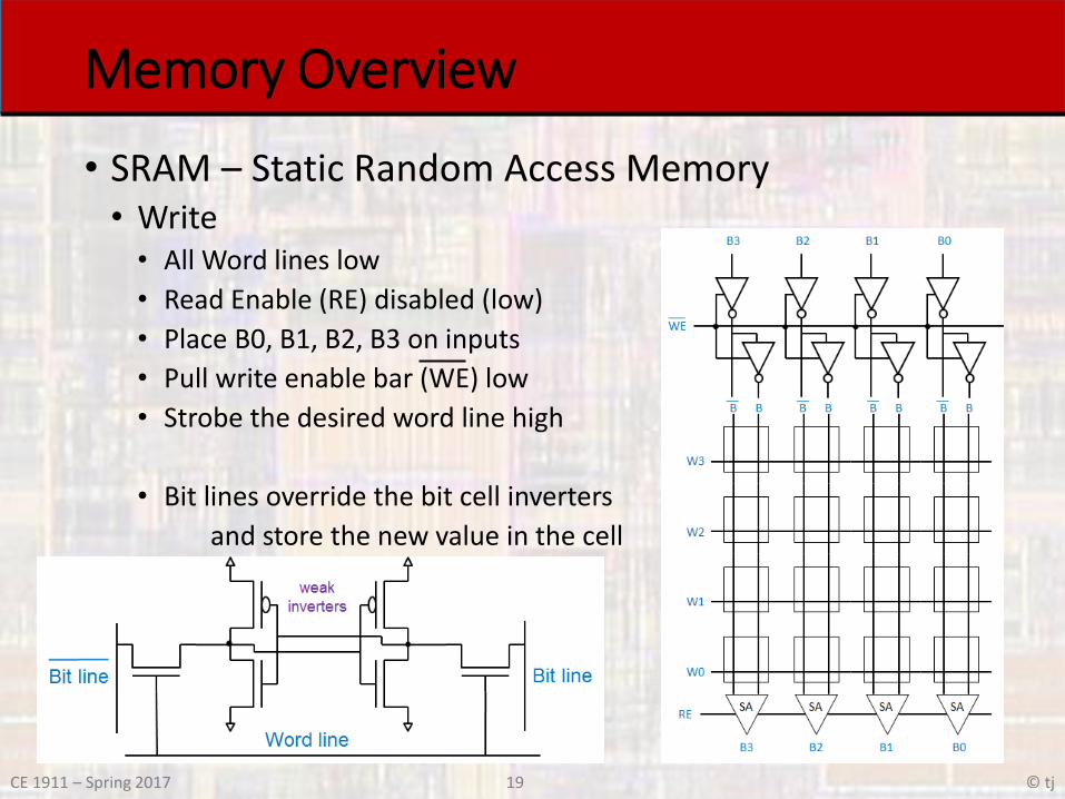
• SRAM – Static Random Access Memory• Write• All Word lines low
• Read Enable (RE) disabled (low)
• Place B0, B1, B2, B3 on inputs
• Pull write enable bar (WE) low
• Strobe the desired word line high
• Bit lines override the bit cell inverters
and store the new value in the cell
20 © tjCE 1911 – Spring 2017
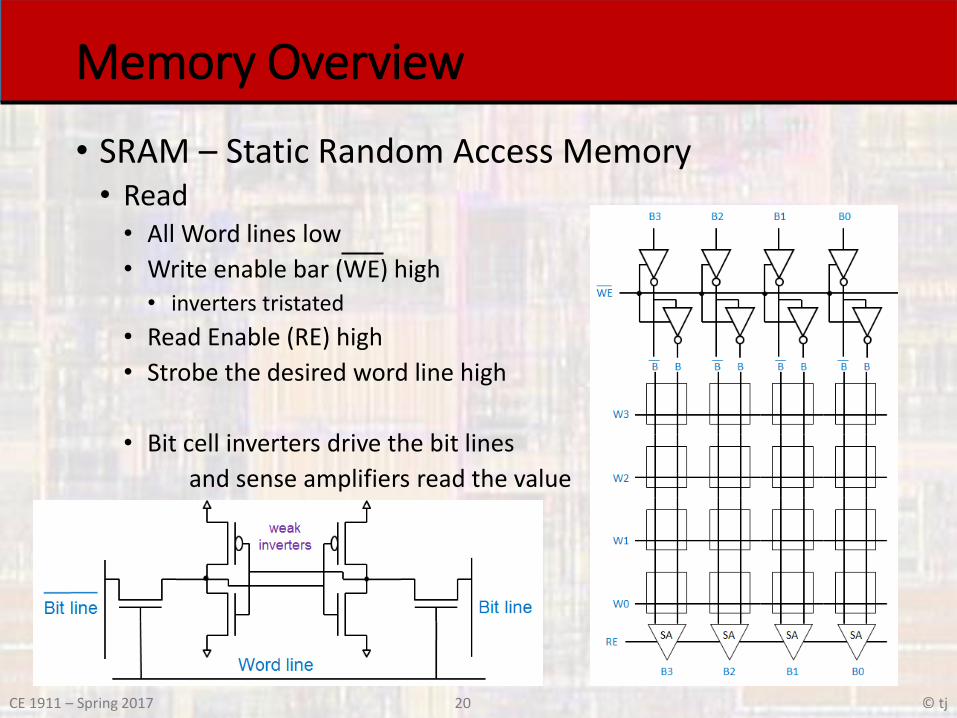
Memory Overview
• SRAM – Static Random Access Memory• Read• All Word lines low
• Write enable bar (WE) high• inverters tristated
• Read Enable (RE) high
• Strobe the desired word line high
• Bit cell inverters drive the bit lines
and sense amplifiers read the value
21 © tjCE 1911 – Spring 2017
Memory Overview
Dynamic Random Access Memory - DRAM
22 © tjCE 1911 – Spring 2017
Memory Overview
• Dynamic Random Access Memory – DRAM
• Synchronous DRAM - SDRAM• Key Attributes• Sequential vs. Random Access
• Read only vs. Read/Write
• Static vs. Dynamic
• Volatile vs. non-Volatile
• Key Measures• Density
• Speed
• Power
• Cost / bit
+
+
23 © tjCE 1911 – Spring 2017
Memory Overview
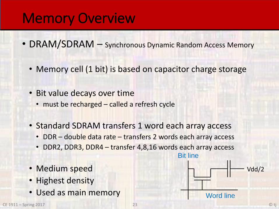
• DRAM/SDRAM – Synchronous Dynamic Random Access Memory
• Memory cell (1 bit) is based on capacitor charge storage
• Bit value decays over time• must be recharged – called a refresh cycle
• Standard SDRAM transfers 1 word each array access• DDR – double data rate – transfers 2 words each array access
• DDR2, DDR3, DDR4 – transfer 4,8,16 words each array access
• Medium speed
• Highest density
• Used as main memory Word line
Bit line
Vdd/2
24 © tjCE 1911 – Spring 2017
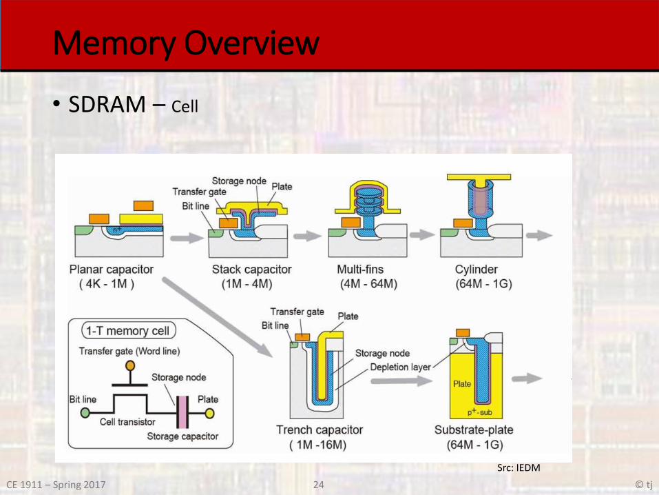
Memory Overview
• SDRAM – Cell
Src: IEDM
25 © tjCE 1911 – Spring 2017
Memory Overview
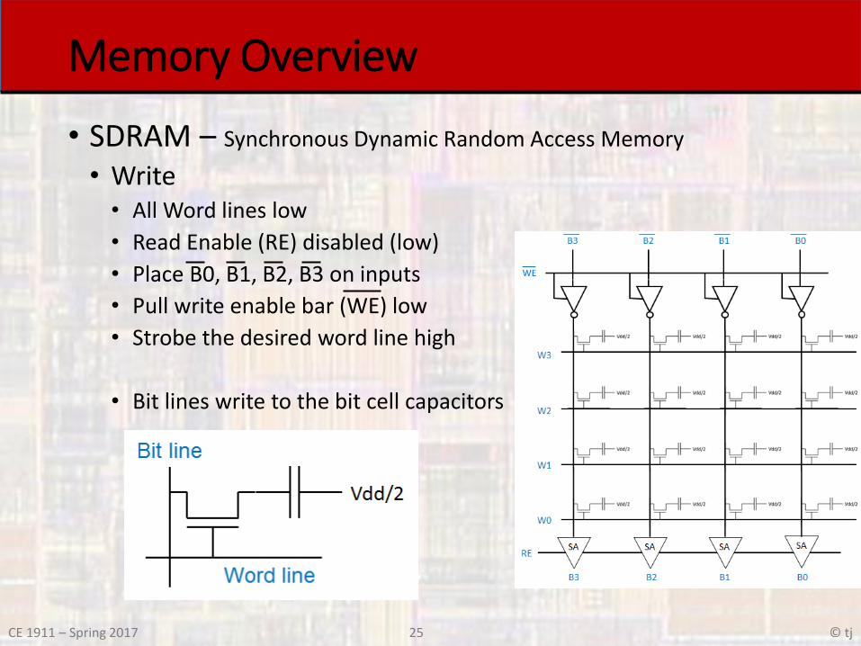
• SDRAM – Synchronous Dynamic Random Access Memory
• Write• All Word lines low
• Read Enable (RE) disabled (low)
• Place B0, B1, B2, B3 on inputs
• Pull write enable bar (WE) low
• Strobe the desired word line high
• Bit lines write to the bit cell capacitors
26 © tjCE 1911 – Spring 2017
Memory Overview
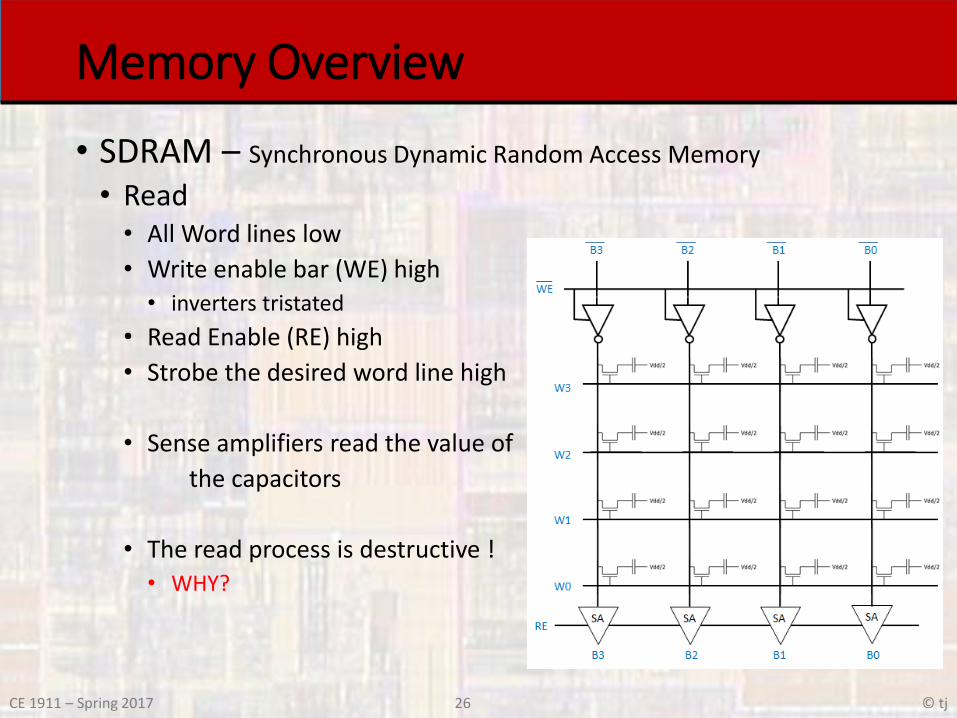
• SDRAM – Synchronous Dynamic Random Access Memory
• Read• All Word lines low
• Write enable bar (WE) high• inverters tristated
• Read Enable (RE) high
• Strobe the desired word line high
• Sense amplifiers read the value of
the capacitors
• The read process is destructive !• WHY?
27 © tjCE 1911 – Spring 2017
Memory Overview
Flash Memory – Nor/Nand Flash
28 © tjCE 1911 – Spring 2017
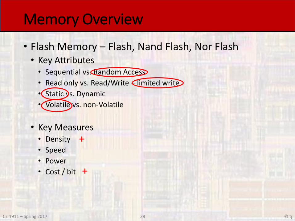
Memory Overview
• Flash Memory – Flash, Nand Flash, Nor Flash• Key Attributes• Sequential vs. Random Access
• Read only vs. Read/Write – limited write
• Static vs. Dynamic
• Volatile vs. non-Volatile
• Key Measures• Density
• Speed
• Power
• Cost / bit
+
+
29 © tjCE 1911 – Spring 2017
Memory Overview
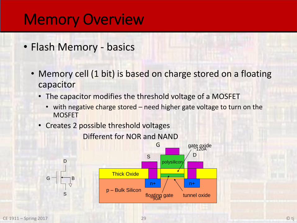
• Flash Memory - basics
• Memory cell (1 bit) is based on charge stored on a floating capacitor• The capacitor modifies the threshold voltage of a MOSFET• with negative charge stored – need higher gate voltage to turn on the
MOSFET
• Creates 2 possible threshold voltages
Different for NOR and NAND
Thick Oxide
polysilicon
n+ n+
p – Bulk Silicontunnel oxide
DS
gate oxide
floating gate
G
D
S
B
G
~90A
~120A
30 © tjCE 1911 – Spring 2017
Memory Overview
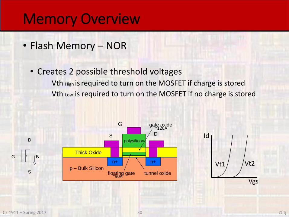
• Flash Memory – NOR
• Creates 2 possible threshold voltages Vth High is required to turn on the MOSFET if charge is stored
Vth Low is required to turn on the MOSFET if no charge is stored
Thick Oxide
polysilicon
n+ n+
p – Bulk Silicontunnel oxide
DS
gate oxide
floating gate
G
D
S
B
G
Id
Vgs
Vt1 Vt2
~90A
~120A
31 © tjCE 1911 – Spring 2017
Memory Overview
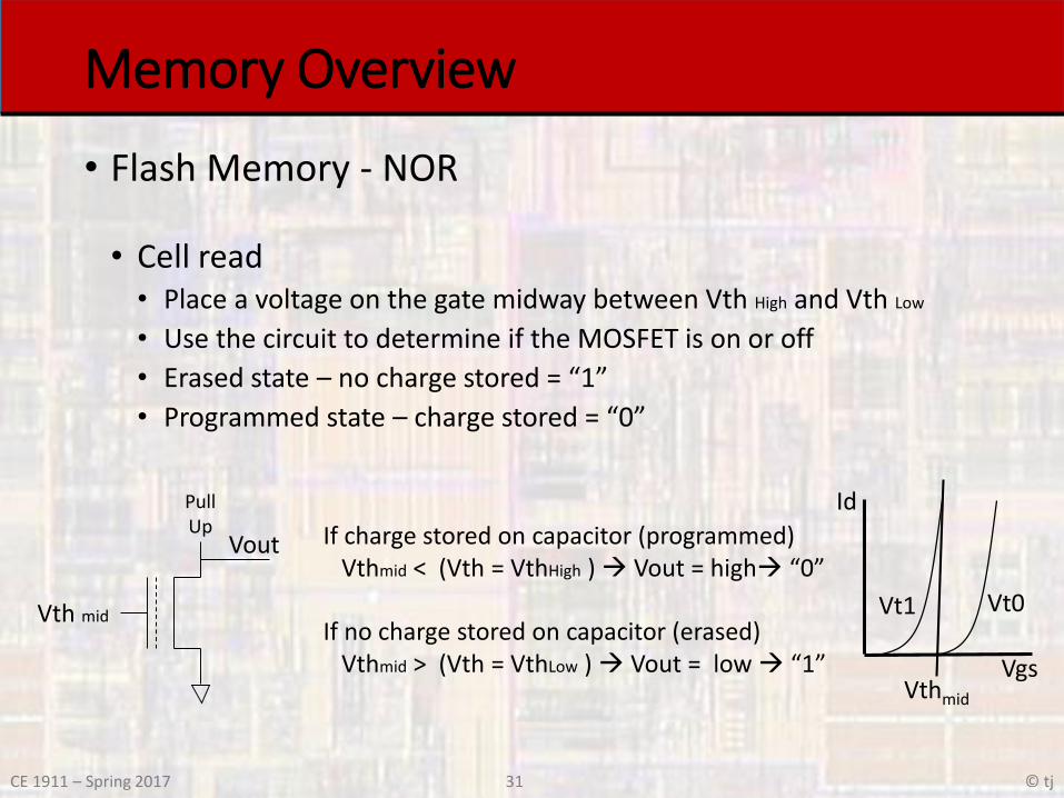
• Flash Memory - NOR
• Cell read• Place a voltage on the gate midway between Vth High and Vth Low
• Use the circuit to determine if the MOSFET is on or off
• Erased state – no charge stored = “1”
• Programmed state – charge stored = “0”
Vth mid
PullUp
Vout If charge stored on capacitor (programmed)Vthmid < (Vth = VthHigh ) Vout = high “0”
If no charge stored on capacitor (erased)Vthmid > (Vth = VthLow ) Vout = low “1”
Id
Vgs
Vt1 Vt0
Vthmid
32 © tjCE 1911 – Spring 2017
Memory Overview
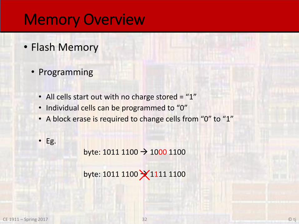
• Flash Memory
• Programming
• All cells start out with no charge stored = “1”
• Individual cells can be programmed to “0”
• A block erase is required to change cells from “0” to “1”
• Eg.
byte: 1011 1100 1000 1100
byte: 1011 1100 1111 1100
33 © tjCE 1911 – Spring 2017
Memory Overview
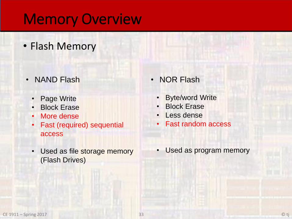
• Flash Memory
• NAND Flash
• Page Write
• Block Erase
• More dense
• Fast (required) sequential
access
• Used as file storage memory
(Flash Drives)
• NOR Flash
• Byte/word Write
• Block Erase
• Less dense
• Fast random access
• Used as program memory
34 © tjCE 1911 – Spring 2017
Memory Overview
• Flash Memory
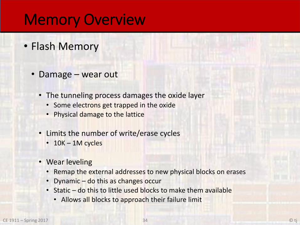
• Damage – wear out
• The tunneling process damages the oxide layer• Some electrons get trapped in the oxide• Physical damage to the lattice
• Limits the number of write/erase cycles• 10K – 1M cycles
• Wear leveling• Remap the external addresses to new physical blocks on erases• Dynamic – do this as changes occur• Static – do this to little used blocks to make them available• Allows all blocks to approach their failure limit
35 © tjCE 1911 – Spring 2017
Memory Overview
• Flash Memory
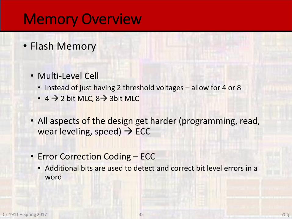
• Multi-Level Cell• Instead of just having 2 threshold voltages – allow for 4 or 8
• 4 2 bit MLC, 8 3bit MLC
• All aspects of the design get harder (programming, read, wear leveling, speed) ECC
• Error Correction Coding – ECC• Additional bits are used to detect and correct bit level errors in a
word
36 © tjCE 1911 – Spring 2017
Memory Overview
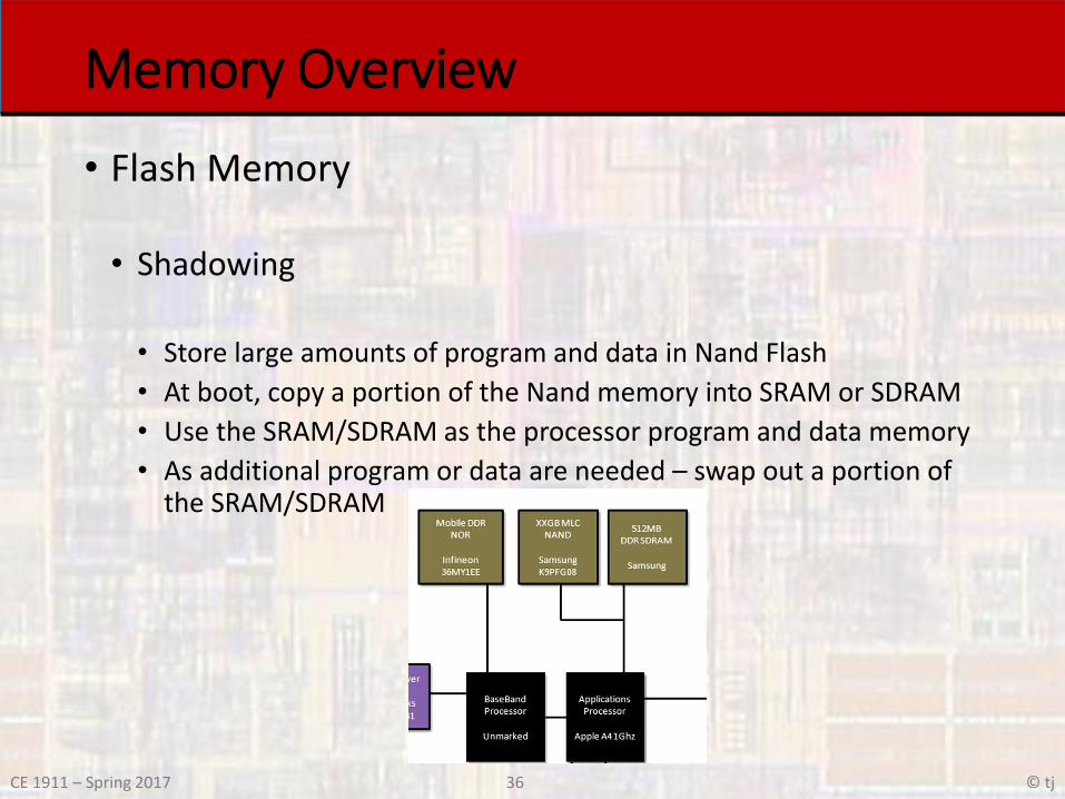
• Flash Memory
• Shadowing
• Store large amounts of program and data in Nand Flash
• At boot, copy a portion of the Nand memory into SRAM or SDRAM
• Use the SRAM/SDRAM as the processor program and data memory
• As additional program or data are needed – swap out a portion of the SRAM/SDRAM
37 © tjCE 1911 – Spring 2017
Memory Overview
• Flash memory
• XIP – Execute in Place
• Execute directly out of NOR flash
• Nor Flash densities are growing rapidly
• Nor Flash speeds are fast enough to support the memory hierarchy
• Requires a caching system
38 © tjCE 1911 – Spring 2017
Memory Overview
• Other Technologies
• Phase Change Memory – PRAM
• Ferro-Magnetic Ram – FeRAM
• Magneto-resistive Ram - MRAM
39 © tjCE 1911 – Spring 2017
Memory Overview
• Performance Issues
• Can 1 bad array element ruin an entire part?
• Use redundant rows and columns in the array• Any bad cells are programmed out at final test
• Some Memory Management Units (MMUs) can detect poorly performing calls and modify the virtual to physical address translation to remove them from the memory map