Embed Size (px)
Citation preview
HAL Id: lirmm-03377249https://hal-lirmm.ccsd.cnrs.fr/lirmm-03377249
Submitted on 14 Oct 2021
HAL is a multi-disciplinary open accessarchive for the deposit and dissemination of sci-entific research documents, whether they are pub-lished or not. The documents may come fromteaching and research institutions in France orabroad, or from public or private research centers.
L’archive ouverte pluridisciplinaire HAL, estdestinée au dépôt et à la diffusion de documentsscientifiques de niveau recherche, publiés ou non,émanant des établissements d’enseignement et derecherche français ou étrangers, des laboratoirespublics ou privés.
Distributed under a Creative Commons Attribution| 4.0 International License
Multi-Level Control of Resistive RAM (RRAM) Using aWrite Termination to Achieve 4 Bits/Cell in High
Resistance StateHassan Aziza, Said Hamdioui, Moritz Fieback, Mottaqiallah Taouil, Mathieu
Moreau, Patrick Girard, Arnaud Virazel, K. Coulié
To cite this version:Hassan Aziza, Said Hamdioui, Moritz Fieback, Mottaqiallah Taouil, Mathieu Moreau, et al.. Multi-Level Control of Resistive RAM (RRAM) Using a Write Termination to Achieve 4 Bits/Cell in HighResistance State. Electronics, MDPI, 2021, 10 (18), pp.#2222. 10.3390/electronics10182222. lirmm-03377249
electronics
Article
Multi-Level Control of Resistive RAM (RRAM) Using a WriteTermination to Achieve 4 Bits/Cell in High Resistance State
Hassan Aziza 1,* , Said Hamdioui 2, Moritz Fieback 2, Mottaqiallah Taouil 2, Mathieu Moreau 1 , Patrick Girard 3,Arnaud Virazel 3 and Karine Coulié 1
Citation: Aziza, H.; Hamdioui, S.;
Fieback, M.; Taouil, M.; Moreau, M.;
Girard, P.; Virazel, A.; Coulié, K.
Multi-Level Control of Resistive RAM
(RRAM) Using a Write Termination to
Achieve 4 Bits/Cell in High
Resistance State. Electronics 2021, 10,
2222. https://doi.org/10.3390/
electronics10182222
Academic Editor: Antonio Di
Bartolomeo
Received: 10 August 2021
Accepted: 7 September 2021
Published: 10 September 2021
Publisher’s Note: MDPI stays neutral
with regard to jurisdictional claims in
published maps and institutional affil-
iations.
Copyright: © 2021 by the authors.
Licensee MDPI, Basel, Switzerland.
This article is an open access article
distributed under the terms and
conditions of the Creative Commons
Attribution (CC BY) license (https://
creativecommons.org/licenses/by/
4.0/).
1 M2NP, UMR CNRS 7334, Aix-Marseille Université, 38 rue Joliot Curie, F-13451 Marseille, France;[email protected] (M.M.); [email protected] (K.C.)
2 Computer Engineering Laboratory, Delft University of Technology, Mekelweg 4,2628 CD Delft, The Netherlands; [email protected] (S.H.); [email protected] (M.F.);[email protected] (M.T.)
3 LIRMM, University of Montpellier/CNRS, F-34095 Montpellier, France; [email protected] (P.G.);[email protected] (A.V.)
* Correspondence: [email protected]
Abstract: RRAM density enhancement is essential not only to gain market share in the highlycompetitive emerging memory sector but also to enable future high-capacity and power-efficientbrain-inspired systems, beyond the capabilities of today’s hardware. In this paper, a novel designscheme is proposed to realize reliable and uniform multi-level cell (MLC) RRAM operation with-out the need of any read verification. RRAM quad-level cell (QLC) capability with 4 bits/cell isdemonstrated for the first time. QLC is implemented based on a strict control of the cell program-ming current of 1T-1R HfO2-based RRAM cells. From a design standpoint, a self-adaptive writetermination circuit is proposed to control the RESET operation and provide an accurate tuning of theanalog resistance value of each cell of a memory array. The different resistance levels are obtained byvarying the compliance current in the RESET direction. Impact of variability on resistance margins issimulated and analyzed quantitatively at the circuit level to guarantee the robustness of the proposedMLC scheme. The minimal resistance margin reported between two consecutive states is 2.1 kΩalong with an average energy consumption and latency of 25 pJ/cell and 1.65 µs, respectively.
Keywords: RRAM; OxRAM multi-level cell; MLC; QLC; write termination; variability; current control
1. Introduction
Memory is an essential component of today’s electronic systems. It is used in anyequipment using a processor such as computers, smart phones, digital cameras, automotivesystems, etc., [1]. Moreover, the unprecedented growth in Internet of Things (IoT) devicesacross all industry verticals continuously generates a massive amount of data whichincreases the demand for even more physical space for memory. This trend is furtheraccelerated due to the booming increase in artificial intelligence (AI) applications andparticularly edge-AI applications which require processing and storage of data at the samephysical location [2]. Different alternative memory concepts have been explored in the lasttwenty years aiming to overcome the major limitations of existing semiconductor memories,i.e., the volatility of RAM’s and the slow programming of flash [3]. Among these emergingtechnologies, resistive RAMs (referred to as RRAM) are believed to be a good choice due tothe advantages of simple structure offering low manufacturing costs, fast switching speed(~10 ns), small feature sizes (<10 nm), compatibility with current CMOS technology, andlow voltage operation [4]. In an attempt to gain market share in these highly competitiveemerging memory sectors, non-volatile memories (NVMs) vendors are trying to squeezemore and more capacity into constantly shrinking silicon dies, thereby optimizing bothstorage density and cost benefits. In general, there are three ways to increase the storage
Electronics 2021, 10, 2222. https://doi.org/10.3390/electronics10182222 https://www.mdpi.com/journal/electronics
Electronics 2021, 10, 2222 2 of 15
density of RRAMs [5]: crossbar structures, 3D integration, and MLC storage. Crossbararchitectures are very challenging to implement. These architectures leverage the non-linearrelationship between voltage and resistance of some RRAM technologies, which is essentialto avoid the integration of a selector at the cell level in order to reach an optimal cell sizeof 4F2 [6]. However, in the absence of an access device, a large amount of leakage current(known as sneak-path current) flowing through unselected cells is inevitable, leading to thelimitation of crossbar array sizes [6]. Regarding 3D, although eight-layer crossbar RRAMprototypes have been demonstrated, many of the manufacture-related issues includinglayer-dependent resistance variability are still not resolved [7]. Compared with the twoabovementioned methods, MLC with its capability of storing more than a single bit ofinformation in a single cell, is considered as one of the most promising properties ofRRAM as it can increase the memory density without much change to current technologies.Alternatively, MLC can be combined with crossbar/3D technologies to reach integrationdensities never seen before. Although MLC relaxes the magnitude of the sneak currentsand voltage drop problems related to crossbar and 3D approaches, the main challengefacing MLC storage is the implementation at the circuit level of programming techniquescapable to tune accurately the analog resistance levels in order to go beyond 3 bits/cell,which is the current limit of the state-of-the-art.
The MLC storage characteristics of RRAM have been reported in many studies [5,8–13].MLC can be implemented by varying the RRAM compliance current during the SETprogramming operation, or by varying the voltage during the RESET (RST) operation, orby varying the pulse widths and amplitudes during SET or RST operations. However,related prior works have the following shortcomings: MLC operation has been validated atthe device level but design implications for MLC at the circuit and system levels remain tobe explored. In particular, programming currents of the order of 500 µA [12] or 1 mA [13]have been reported at the device level which is incompatible with low power RRAMapplications. Only a few studies of the prior art explore applications of MLC at the circuitlevel [14]. Most of the work focuses on read-out circuits [15–17]. Thereby, RRAM variabilityat the memory array level is not accounted during MLC programming operations. Also, sofar, all the proposed solutions are limited to 3 bits/cell [18]. The proposed study advancesthe state-of-the-art by proposing a new design scheme that enables 4 bits/cell. To theauthors’ knowledge, this is the first work addressing quad-level cell (QLC) operation. Thestudy also introduces compelling MLC features that are missing or poorly achieved inother previously proposed works, including:
• A MLC architecture based on compliance current control during the RST operation,allowing a tight control of post-programming resistances for optimal robustness.The compliance current being defined as the minimal current allowed during theRST operation.
• An implementation at the circuit level with a minimal area overhead (i.e., dozens oftransistors per bit-line) as no specialized read verification circuits are required.
• A minimal energy consumption as high resistance levels (i.e., HRS RRAM states)are targeted.
The remainder of this paper is organized as follows. Section 2 presents the RRAMtechnology along with conventional MLC approaches. In Section 3, the MLC design schemeimplementation is presented. Section 4 presents simulation results. Section 5 discusses theproposed MLC strategy. Finally, Section 6 concludes this paper.
2. OxRAM Technology vs. MLC Modes
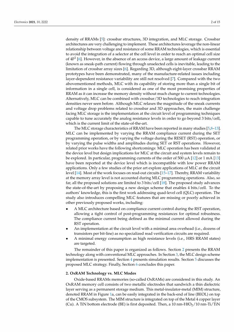
Oxide-based RRAMs memories (so-called OxRAMs) are considered in this study. AnOxRAM memory cell consists of two metallic electrodes that sandwich a thin dielectriclayer serving as a permanent storage medium. This metal-insulator-metal (MIM) structure,denoted RRAM in Figure 1a, can be easily integrated in the back-end of line (BEOL) on topof the CMOS subsystem. The MIM structure is integrated on top of the Metal 4 copper layer(Cu). A TiN bottom electrode (BE) is first deposited. Then, a 10 nm-HfO2/10 nm-Ti/TiN
Electronics 2021, 10, 2222 3 of 15
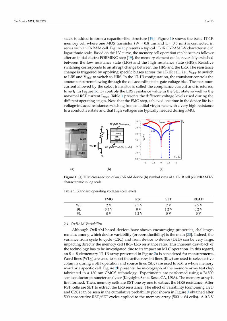
stack is added to form a capacitor-like structure [19]. Figure 1b shows the basic 1T-1Rmemory cell where one MOS transistor (W = 0.8 µm and L = 0.5 µm) is connected inseries with an OxRAM cell. Figure 1c presents a typical 1T-1R OxRAM I-V characteristic inlogarithmic scale. Based on the I-V curve, the memory cell operation can be seen as follows:after an initial electro-FORMING step [19], the memory element can be reversibly switchedbetween the low resistance state (LRS) and the high resistance state (HRS). Resistiveswitching corresponds to an abrupt change between the HRS and the LRS. The resistancechange is triggered by applying specific biases across the 1T-1R cell, i.e., VSET to switchto LRS and VRST to switch to HRS. In the 1T-1R configuration, the transistor controls theamount of current flowing through the cell according to its gate voltage bias. The maximumcurrent allowed by the select transistor is called the compliance current and is referredto as IC in Figure 1c. IC controls the LRS resistance value in the SET state as well as themaximal RST current Ireset. Table 1 presents the different voltage levels used during thedifferent operating stages. Note that the FMG step, achieved one time in the device life is avoltage-induced resistance switching from an initial virgin state with a very high resistanceto a conductive state and that high voltages are typically needed during FMG.
Electronics 2021, 10, x FOR PEER REVIEW 3 of 15
on top of the CMOS subsystem. The MIM structure is integrated on top of the Metal 4 copper layer (Cu). A TiN bottom electrode (BE) is first deposited. Then, a 10 nm-HfO2/10 nm-Ti/TiN stack is added to form a capacitor-like structure [19]. Figure 1b shows the basic 1T-1R memory cell where one MOS transistor (W = 0.8 μm and L = 0.5 μm) is connected in series with an OxRAM cell. Figure 1c presents a typical 1T-1R OxRAM I-V characteristic in logarithmic scale. Based on the I-V curve, the memory cell operation can be seen as follows: after an initial electro-FORMING step [19], the memory element can be reversibly switched between the low resistance state (LRS) and the high resistance state (HRS). Re-sistive switching corresponds to an abrupt change between the HRS and the LRS. The resistance change is triggered by applying specific biases across the 1T-1R cell, i.e., VSET to switch to LRS and VRST to switch to HRS. In the 1T-1R configuration, the transistor controls the amount of current flowing through the cell according to its gate voltage bias. The max-imum current allowed by the select transistor is called the compliance current and is re-ferred to as IC in Figure 1c. IC controls the LRS resistance value in the SET state as well as the maximal RST current Ireset. Table 1 presents the different voltage levels used during the different operating stages. Note that the FMG step, achieved one time in the device life is a voltage-induced resistance switching from an initial virgin state with a very high re-sistance to a conductive state and that high voltages are typically needed during FMG.
(a) (b) (c)
Figure 1. (a) TEM cross-section of an OxRAM device (b) symbol view of a 1T-1R cell (c) OxRAM I-V characteristic in log scale.
Table 1. Standard operating voltages (cell level).
FMG RST SET READ WL 2 V 2.5 V 2 V 2.5 V BL 3.3 V 0 V 1.2 V 0.2 V SL 0 V 1.2 V 0 V 0 V
2.1. OxRAM Variability Although OxRAM-based devices have shown encouraging properties, challenges re-
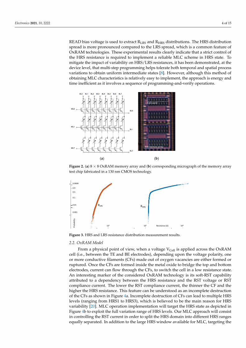
main, among which device variability (or reproducibility) is the main [20]. Indeed, the variance from cycle to cycle (C2C) and from device to device (D2D) can be very large, impacting directly the memory cell HRS/LRS resistance ratio. This inherent drawback of the technology has to be investigated due to its impact on MLC operation. In this regard, an 8 × 8 elementary 1T-1R array presented in Figure 2a is considered for measurements. Word lines (WLX) are used to select the active row, bit lines (BLX) are used to select active columns during a SET operation and source lines (SLX) are used to RST a whole memory word or a specific cell. Figure 2b presents the micrograph of the memory array test chip fabricated in a 130 nm CMOS technology. Experiments are performed using a B1500 sem-iconductor parameter analyzer (Keysight, Santa Rosa, CA, USA). The memory array is first formed. Then, memory cells are RST one by one to extract the HRS resistance. After
WL
SL
BLTE (TOP Electrode)
BE (BOTTOM Electrode)
Hf02(10nm)
Ti (10nm)
TiN
TiN
VBL (V)
I BL(A
)
-1 -0.5 0 0.5 1
10-6
10-9
10-3
10-4
10-5
10-7
10-8
ICIreset
Figure 1. (a) TEM cross-section of an OxRAM device (b) symbol view of a 1T-1R cell (c) OxRAM I-Vcharacteristic in log scale.
Table 1. Standard operating voltages (cell level).
FMG RST SET READ
WL 2 V 2.5 V 2 V 2.5 VBL 3.3 V 0 V 1.2 V 0.2 VSL 0 V 1.2 V 0 V 0 V
2.1. OxRAM Variability
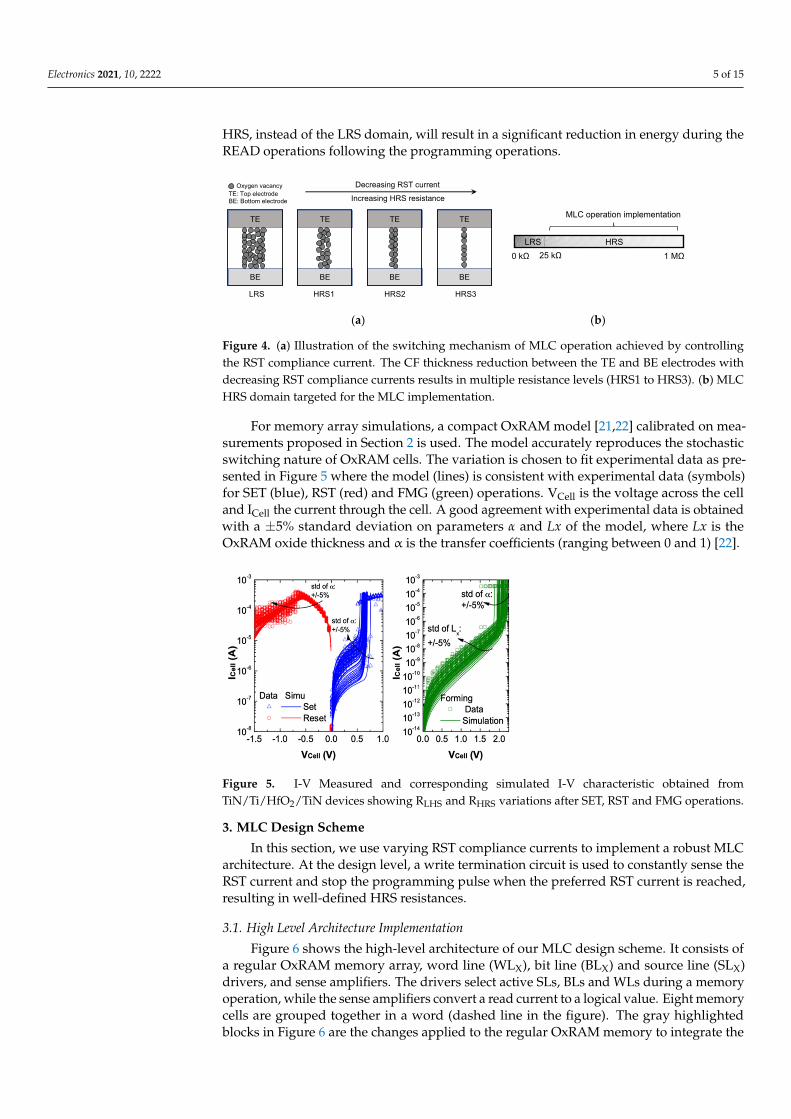
Although OxRAM-based devices have shown encouraging properties, challengesremain, among which device variability (or reproducibility) is the main [20]. Indeed, thevariance from cycle to cycle (C2C) and from device to device (D2D) can be very large,impacting directly the memory cell HRS/LRS resistance ratio. This inherent drawback ofthe technology has to be investigated due to its impact on MLC operation. In this regard,an 8 × 8 elementary 1T-1R array presented in Figure 2a is considered for measurements.Word lines (WLX) are used to select the active row, bit lines (BLX) are used to select activecolumns during a SET operation and source lines (SLX) are used to RST a whole memoryword or a specific cell. Figure 2b presents the micrograph of the memory array test chipfabricated in a 130 nm CMOS technology. Experiments are performed using a B1500semiconductor parameter analyzer (Keysight, Santa Rosa, CA, USA). The memory array isfirst formed. Then, memory cells are RST one by one to extract the HRS resistance. AfterRST, cells are SET to extract the LRS resistance. The effect of variability (combining D2Dand C2C) can be seen in the cumulative probability plot shown in Figure 3 obtained after500 consecutive RST/SET cycles applied to the memory array (500 × 64 cells). A 0.3 V
Electronics 2021, 10, 2222 4 of 15
READ bias voltage is used to extract RLRS and RHRS distributions. The HRS distributionspread is more pronounced compared to the LRS spread, which is a common feature ofOxRAM technologies. These experimental results clearly indicate that a strict control ofthe HRS resistance is required to implement a reliable MLC scheme in HRS state. Tomitigate the impact of variability on HRS/LRS resistances, it has been demonstrated, at thedevice level, that multi-step programming helps tolerate both temporal and spatial processvariations to obtain uniform intermediate states [8]. However, although this method ofobtaining MLC characteristics is relatively easy to implement, the approach is energy andtime inefficient as it involves a sequence of programming-and-verify operations.
Electronics 2021, 10, x FOR PEER REVIEW 4 of 15
RST, cells are SET to extract the LRS resistance. The effect of variability (combining D2D and C2C) can be seen in the cumulative probability plot shown in Figure 3 obtained after 500 consecutive RST/SET cycles applied to the memory array (500 × 64 cells). A 0.3 V READ bias voltage is used to extract RLRS and RHRS distributions. The HRS distribution spread is more pronounced compared to the LRS spread, which is a common feature of OxRAM technologies. These experimental results clearly indicate that a strict control of the HRS resistance is required to implement a reliable MLC scheme in HRS state. To mit-igate the impact of variability on HRS/LRS resistances, it has been demonstrated, at the device level, that multi-step programming helps tolerate both temporal and spatial pro-cess variations to obtain uniform intermediate states [8]. However, although this method of obtaining MLC characteristics is relatively easy to implement, the approach is energy and time inefficient as it involves a sequence of programming-and-verify operations.
(a) (b)
Figure 2. (a) 8 × 8 OxRAM memory array and (b) corresponding micrograph of the memory array test chip fabricated in a 130 nm CMOS technology.
Figure 3. HRS and LRS resistance distribution measurement results.
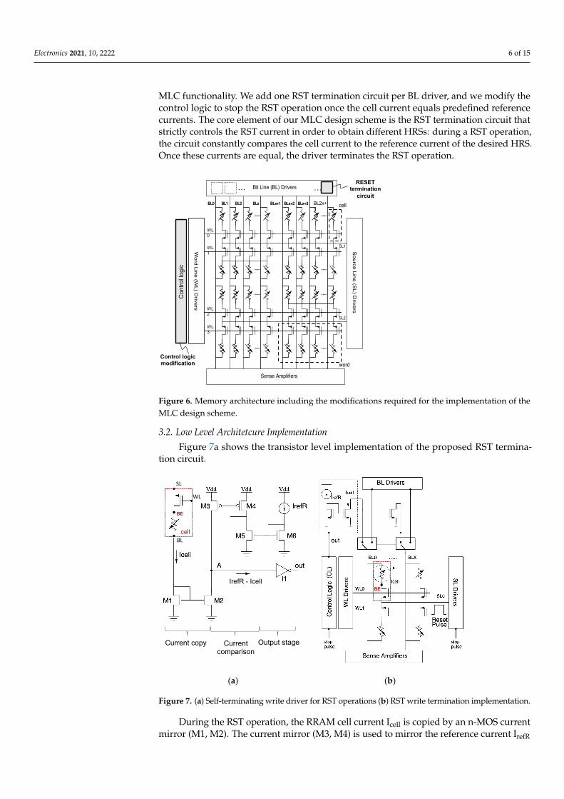
2.2. OxRAM Model From a physical point of view, when a voltage VCell is applied across the OxRAM cell
(i.e., between the TE and BE electrodes), depending upon the voltage polarity, one or more conductive filaments (CFs) made out of oxygen vacancies are either formed or ruptured. Once the CFs are formed inside the metal oxide to bridge the top and bottom electrodes, current can flow through the CFs, to switch the cell in a low resistance state. An interesting marker of the considered OxRAM technology is its soft-RST capability attributed to a de-pendency between the HRS resistance and the RST voltage or RST compliance current. The lower the RST compliance current, the thinner the CF and the higher the HRS re-sistance. This feature can be understood as an incomplete destruction of the CFs as shown in Figure 4a. Incomplete destruction of CFs can lead to multiple HRS levels (ranging from HRS1 to HRS3), which is believed to be the main reason for HRS variability [20]. MLC operation implementation will target the HRS state as depicted in Figure 4b to exploit the
8-bit word
8x8 memory array
104 105 106Resistance (Ω)Prob
abili
ty
0.9999
0.1
0.5
0.01
0.001
0.9
RLRS RHRS
Figure 2. (a) 8 × 8 OxRAM memory array and (b) corresponding micrograph of the memory arraytest chip fabricated in a 130 nm CMOS technology.
Electronics 2021, 10, x FOR PEER REVIEW 4 of 15
RST, cells are SET to extract the LRS resistance. The effect of variability (combining D2D and C2C) can be seen in the cumulative probability plot shown in Figure 3 obtained after 500 consecutive RST/SET cycles applied to the memory array (500 × 64 cells). A 0.3 V READ bias voltage is used to extract RLRS and RHRS distributions. The HRS distribution spread is more pronounced compared to the LRS spread, which is a common feature of OxRAM technologies. These experimental results clearly indicate that a strict control of the HRS resistance is required to implement a reliable MLC scheme in HRS state. To mit-igate the impact of variability on HRS/LRS resistances, it has been demonstrated, at the device level, that multi-step programming helps tolerate both temporal and spatial pro-cess variations to obtain uniform intermediate states [8]. However, although this method of obtaining MLC characteristics is relatively easy to implement, the approach is energy and time inefficient as it involves a sequence of programming-and-verify operations.
(a) (b)
Figure 2. (a) 8 × 8 OxRAM memory array and (b) corresponding micrograph of the memory array test chip fabricated in a 130 nm CMOS technology.
Figure 3. HRS and LRS resistance distribution measurement results.
2.2. OxRAM Model From a physical point of view, when a voltage VCell is applied across the OxRAM cell
(i.e., between the TE and BE electrodes), depending upon the voltage polarity, one or more conductive filaments (CFs) made out of oxygen vacancies are either formed or ruptured. Once the CFs are formed inside the metal oxide to bridge the top and bottom electrodes, current can flow through the CFs, to switch the cell in a low resistance state. An interesting marker of the considered OxRAM technology is its soft-RST capability attributed to a de-pendency between the HRS resistance and the RST voltage or RST compliance current. The lower the RST compliance current, the thinner the CF and the higher the HRS re-sistance. This feature can be understood as an incomplete destruction of the CFs as shown in Figure 4a. Incomplete destruction of CFs can lead to multiple HRS levels (ranging from HRS1 to HRS3), which is believed to be the main reason for HRS variability [20]. MLC operation implementation will target the HRS state as depicted in Figure 4b to exploit the
8-bit word
8x8 memory array
104 105 106Resistance (Ω)Prob
abili
ty
0.9999
0.1
0.5
0.01
0.001
0.9
RLRS RHRS
Figure 3. HRS and LRS resistance distribution measurement results.
2.2. OxRAM Model
From a physical point of view, when a voltage VCell is applied across the OxRAMcell (i.e., between the TE and BE electrodes), depending upon the voltage polarity, oneor more conductive filaments (CFs) made out of oxygen vacancies are either formed orruptured. Once the CFs are formed inside the metal oxide to bridge the top and bottomelectrodes, current can flow through the CFs, to switch the cell in a low resistance state.An interesting marker of the considered OxRAM technology is its soft-RST capabilityattributed to a dependency between the HRS resistance and the RST voltage or RSTcompliance current. The lower the RST compliance current, the thinner the CF and thehigher the HRS resistance. This feature can be understood as an incomplete destructionof the CFs as shown in Figure 4a. Incomplete destruction of CFs can lead to multiple HRSlevels (ranging from HRS1 to HRS3), which is believed to be the main reason for HRSvariability [20]. MLC operation implementation will target the HRS state as depicted inFigure 4b to exploit the full variation range of HRS levels. Our MLC approach will consistin controlling the RST current in order to split the HRS domain into different HRS rangesequally separated. In addition to the large HRS window available for MLC, targeting the
Electronics 2021, 10, 2222 5 of 15
HRS, instead of the LRS domain, will result in a significant reduction in energy during theREAD operations following the programming operations.
Electronics 2021, 10, x FOR PEER REVIEW 5 of 15
full variation range of HRS levels. Our MLC approach will consist in controlling the RST current in order to split the HRS domain into different HRS ranges equally separated. In addition to the large HRS window available for MLC, targeting the HRS, instead of the LRS domain, will result in a significant reduction in energy during the READ operations following the programming operations.
(a) (b)
Figure 4. (a) Illustration of the switching mechanism of MLC operation achieved by controlling the RST compliance current. The CF thickness reduction between the TE and BE electrodes with de-creasing RST compliance currents results in multiple resistance levels (HRS1 to HRS3). (b) MLC HRS domain targeted for the MLC implementation.
For memory array simulations, a compact OxRAM model [21,22] calibrated on meas-urements proposed in Section 2 is used. The model accurately reproduces the stochastic switching nature of OxRAM cells. The variation is chosen to fit experimental data as pre-sented in Figure 5 where the model (lines) is consistent with experimental data (symbols) for SET (blue), RST (red) and FMG (green) operations. VCell is the voltage across the cell and ICell the current through the cell. A good agreement with experimental data is obtained with a ±5% standard deviation on parameters α and Lx of the model, where Lx is the Ox-RAM oxide thickness and α is the transfer coefficients (ranging between 0 and 1) [22].
Figure 5. I-V Measured and corresponding simulated I–V characteristic obtained from TiN/Ti/HfO2/TiN devices showing RLHS and RHRS variations after SET, RST and FMG operations.
3. MLC Design Scheme In this section, we use varying RST compliance currents to implement a robust MLC
architecture. At the design level, a write termination circuit is used to constantly sense the RST current and stop the programming pulse when the preferred RST current is reached, resulting in well-defined HRS resistances.
3.1. High Level Architecture Implementation Figure 6 shows the high-level architecture of our MLC design scheme. It consists of
a regular OxRAM memory array, word line (WLX), bit line (BLX) and source line (SLX) drivers, and sense amplifiers. The drivers select active SLs, BLs and WLs during a memory
TE
BE
TE
BE
TE
BE
TE
BE
Decreasing RST current
Increasing HRS resistance
LRS HRS1 HRS2 HRS3
Oxygen vacancyTE: Top electrodeBE: Bottom electrode
0 kΩ 1 MΩLRS HRS
25 kΩ
MLC operation implementation
Figure 4. (a) Illustration of the switching mechanism of MLC operation achieved by controllingthe RST compliance current. The CF thickness reduction between the TE and BE electrodes withdecreasing RST compliance currents results in multiple resistance levels (HRS1 to HRS3). (b) MLCHRS domain targeted for the MLC implementation.
For memory array simulations, a compact OxRAM model [21,22] calibrated on mea-surements proposed in Section 2 is used. The model accurately reproduces the stochasticswitching nature of OxRAM cells. The variation is chosen to fit experimental data as pre-sented in Figure 5 where the model (lines) is consistent with experimental data (symbols)for SET (blue), RST (red) and FMG (green) operations. VCell is the voltage across the celland ICell the current through the cell. A good agreement with experimental data is obtainedwith a ±5% standard deviation on parameters α and Lx of the model, where Lx is theOxRAM oxide thickness and α is the transfer coefficients (ranging between 0 and 1) [22].
Electronics 2021, 10, x FOR PEER REVIEW 5 of 15
full variation range of HRS levels. Our MLC approach will consist in controlling the RST current in order to split the HRS domain into different HRS ranges equally separated. In addition to the large HRS window available for MLC, targeting the HRS, instead of the LRS domain, will result in a significant reduction in energy during the READ operations following the programming operations.
(a) (b)
Figure 4. (a) Illustration of the switching mechanism of MLC operation achieved by controlling the RST compliance current. The CF thickness reduction between the TE and BE electrodes with de-creasing RST compliance currents results in multiple resistance levels (HRS1 to HRS3). (b) MLC HRS domain targeted for the MLC implementation.
For memory array simulations, a compact OxRAM model [21,22] calibrated on meas-urements proposed in Section 2 is used. The model accurately reproduces the stochastic switching nature of OxRAM cells. The variation is chosen to fit experimental data as pre-sented in Figure 5 where the model (lines) is consistent with experimental data (symbols) for SET (blue), RST (red) and FMG (green) operations. VCell is the voltage across the cell and ICell the current through the cell. A good agreement with experimental data is obtained with a ±5% standard deviation on parameters α and Lx of the model, where Lx is the Ox-RAM oxide thickness and α is the transfer coefficients (ranging between 0 and 1) [22].
Figure 5. I-V Measured and corresponding simulated I–V characteristic obtained from TiN/Ti/HfO2/TiN devices showing RLHS and RHRS variations after SET, RST and FMG operations.
3. MLC Design Scheme In this section, we use varying RST compliance currents to implement a robust MLC
architecture. At the design level, a write termination circuit is used to constantly sense the RST current and stop the programming pulse when the preferred RST current is reached, resulting in well-defined HRS resistances.
3.1. High Level Architecture Implementation Figure 6 shows the high-level architecture of our MLC design scheme. It consists of
a regular OxRAM memory array, word line (WLX), bit line (BLX) and source line (SLX) drivers, and sense amplifiers. The drivers select active SLs, BLs and WLs during a memory
TE
BE
TE
BE
TE
BE
TE
BE
Decreasing RST current
Increasing HRS resistance
LRS HRS1 HRS2 HRS3
Oxygen vacancyTE: Top electrodeBE: Bottom electrode
0 kΩ 1 MΩLRS HRS
25 kΩ
MLC operation implementation
Figure 5. I-V Measured and corresponding simulated I-V characteristic obtained fromTiN/Ti/HfO2/TiN devices showing RLHS and RHRS variations after SET, RST and FMG operations.
3. MLC Design Scheme
In this section, we use varying RST compliance currents to implement a robust MLCarchitecture. At the design level, a write termination circuit is used to constantly sense theRST current and stop the programming pulse when the preferred RST current is reached,resulting in well-defined HRS resistances.
3.1. High Level Architecture Implementation
Figure 6 shows the high-level architecture of our MLC design scheme. It consists ofa regular OxRAM memory array, word line (WLX), bit line (BLX) and source line (SLX)drivers, and sense amplifiers. The drivers select active SLs, BLs and WLs during a memoryoperation, while the sense amplifiers convert a read current to a logical value. Eight memorycells are grouped together in a word (dashed line in the figure). The gray highlightedblocks in Figure 6 are the changes applied to the regular OxRAM memory to integrate the
Electronics 2021, 10, 2222 6 of 15
MLC functionality. We add one RST termination circuit per BL driver, and we modify thecontrol logic to stop the RST operation once the cell current equals predefined referencecurrents. The core element of our MLC design scheme is the RST termination circuit thatstrictly controls the RST current in order to obtain different HRSs: during a RST operation,the circuit constantly compares the cell current to the reference current of the desired HRS.Once these currents are equal, the driver terminates the RST operation.
Electronics 2021, 10, x FOR PEER REVIEW 6 of 15
operation, while the sense amplifiers convert a read current to a logical value. Eight memory cells are grouped together in a word (dashed line in the figure). The gray high-lighted blocks in Figure 6 are the changes applied to the regular OxRAM memory to inte-grate the MLC functionality. We add one RST termination circuit per BL driver, and we modify the control logic to stop the RST operation once the cell current equals predefined reference currents. The core element of our MLC design scheme is the RST termination circuit that strictly controls the RST current in order to obtain different HRSs: during a RST operation, the circuit constantly compares the cell current to the reference current of the desired HRS. Once these currents are equal, the driver terminates the RST operation.
Figure 6. Memory architecture including the modifications required for the implementation of the MLC design scheme.
3.2. Low Level Architetcure Implementation Figure 7a shows the transistor level implementation of the proposed RST termination
circuit.
(a) (b)
Figure 7. (a) Self-terminating write driver for RST operations (b) RST write termination implemen-tation.
Output stage
BLcell
WL
Current copy Current comparison
IrefR - Icell
SL
BE
BE
Figure 6. Memory architecture including the modifications required for the implementation of theMLC design scheme.
3.2. Low Level Architetcure Implementation
Figure 7a shows the transistor level implementation of the proposed RST termina-tion circuit.
Electronics 2021, 10, x FOR PEER REVIEW 6 of 15
operation, while the sense amplifiers convert a read current to a logical value. Eight memory cells are grouped together in a word (dashed line in the figure). The gray high-lighted blocks in Figure 6 are the changes applied to the regular OxRAM memory to inte-grate the MLC functionality. We add one RST termination circuit per BL driver, and we modify the control logic to stop the RST operation once the cell current equals predefined reference currents. The core element of our MLC design scheme is the RST termination circuit that strictly controls the RST current in order to obtain different HRSs: during a RST operation, the circuit constantly compares the cell current to the reference current of the desired HRS. Once these currents are equal, the driver terminates the RST operation.
Figure 6. Memory architecture including the modifications required for the implementation of the MLC design scheme.
3.2. Low Level Architetcure Implementation Figure 7a shows the transistor level implementation of the proposed RST termination
circuit.
(a) (b)
Figure 7. (a) Self-terminating write driver for RST operations (b) RST write termination implemen-tation.
Output stage
BLcell
WL
Current copy Current comparison
IrefR - Icell
SL
BE
BE
Figure 7. (a) Self-terminating write driver for RST operations (b) RST write termination implementation.
During the RST operation, the RRAM cell current Icell is copied by an n-MOS currentmirror (M1, M2). The current mirror (M3, M4) is used to mirror the reference current IrefR
Electronics 2021, 10, 2222 7 of 15
(provided by M5, M6) which feeds the input of inverter I1. If (Icell − IrefR) > 0, the inverterinput A is set low and the comparator output out is set to high. If (Icell − IrefR) < 0, inputA is set high and out is set to low to terminate the RST operation (i.e., the RST operationis terminated when Icell decreases down to IrefR). IrefR is derived from a bandgap voltagereference circuit that is also included in a regular memory architecture to achieve stabilityover process, voltage and temperature [23].
Note that the RST process is a negative feedback mechanism: as the current flows fromthe BE to the BL, the cell resistance increases, causing current to reduce. In contrast, theSET operation is a positive feedback mechanism: as the current flows, the cell resistance isreduced, and as such, more current flows. Hence, a SET operation requires a current limita-tion to prevent a breakdown of the device. However, when considering MLC operation forthe HRS, it is beneficial to control the RST current and terminate the RST operation whenthe cell current reaches a predefined minimal current, as a limit is set for the HRS resistance(i.e., the lower limit of the current is the upper limit of the HRS resistance). Figure 7b showsthe usage of the termination circuit in the memory architecture. For clarity, we only showthe current copy stage of the RST termination circuit. The RST operation is performed bybiasing the memory cell through the SL driver while WL0 is activated. BL0 connects to thecurrent copy stage of Figure 7a and sinks the cell current. When Icell equals IrefR (i.e., outsignal is set low), the control logic triggers a stop pulse to the SL driver to terminate theRST operation.
4. Circuit Level Evaluation4.1. MLC Concept
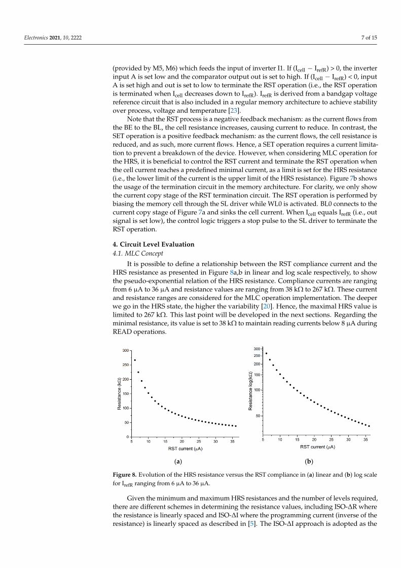
It is possible to define a relationship between the RST compliance current and theHRS resistance as presented in Figure 8a,b in linear and log scale respectively, to showthe pseudo-exponential relation of the HRS resistance. Compliance currents are rangingfrom 6 µA to 36 µA and resistance values are ranging from 38 kΩ to 267 kΩ. These currentand resistance ranges are considered for the MLC operation implementation. The deeperwe go in the HRS state, the higher the variability [20]. Hence, the maximal HRS value islimited to 267 kΩ. This last point will be developed in the next sections. Regarding theminimal resistance, its value is set to 38 kΩ to maintain reading currents below 8 µA duringREAD operations.
Electronics 2021, 10, x FOR PEER REVIEW 7 of 15
During the RST operation, the RRAM cell current Icell is copied by an n-MOS current mirror (M1, M2). The current mirror (M3, M4) is used to mirror the reference current IrefR (provided by M5, M6) which feeds the input of inverter I1. If (Icell − IrefR) > 0, the inverter input A is set low and the comparator output out is set to high. If (Icell − IrefR) < 0, input A is set high and out is set to low to terminate the RST operation (i.e., the RST operation is terminated when Icell decreases down to IrefR). IrefR is derived from a bandgap voltage ref-erence circuit that is also included in a regular memory architecture to achieve stability over process, voltage and temperature [23].
Note that the RST process is a negative feedback mechanism: as the current flows from the BE to the BL, the cell resistance increases, causing current to reduce. In contrast, the SET operation is a positive feedback mechanism: as the current flows, the cell re-sistance is reduced, and as such, more current flows. Hence, a SET operation requires a current limitation to prevent a breakdown of the device. However, when considering MLC operation for the HRS, it is beneficial to control the RST current and terminate the RST operation when the cell current reaches a predefined minimal current, as a limit is set for the HRS resistance (i.e., the lower limit of the current is the upper limit of the HRS resistance). Figure 7b shows the usage of the termination circuit in the memory architec-ture. For clarity, we only show the current copy stage of the RST termination circuit. The RST operation is performed by biasing the memory cell through the SL driver while WL0 is activated. BL0 connects to the current copy stage of Figure 7a and sinks the cell current. When Icell equals IrefR (i.e., out signal is set low), the control logic triggers a stop pulse to the SL driver to terminate the RST operation.
4. Circuit Level Evaluation 4.1. MLC Concept
It is possible to define a relationship between the RST compliance current and the HRS resistance as presented in Figure 8a,b in linear and log scale respectively, to show the pseudo-exponential relation of the HRS resistance. Compliance currents are ranging from 6 μA to 36 μA and resistance values are ranging from 38 kΩ to 267 kΩ. These current and resistance ranges are considered for the MLC operation implementation. The deeper we go in the HRS state, the higher the variability [20]. Hence, the maximal HRS value is lim-ited to 267 kΩ. This last point will be developed in the next sections. Regarding the mini-mal resistance, its value is set to 38 kΩ to maintain reading currents below 8 μA during READ operations.
(a) (b)
Figure 8. Evolution of the HRS resistance versus the RST compliance in (a) linear and (b) log scale for IrefR ranging from 6 μA to 36 μA.
Given the minimum and maximum HRS resistances and the number of levels re-quired, there are different schemes in determining the resistance values, including ISO-
Figure 8. Evolution of the HRS resistance versus the RST compliance in (a) linear and (b) log scalefor IrefR ranging from 6 µA to 36 µA.
Given the minimum and maximum HRS resistances and the number of levels required,there are different schemes in determining the resistance values, including ISO-∆R wherethe resistance is linearly spaced and ISO-∆I where the programming current (inverse of theresistance) is linearly spaced as described in [5]. The ISO-∆I approach is adopted as the
Electronics 2021, 10, 2222 8 of 15
proposed MLC scheme is based on RST current control. Table 2 presents the 16 differentbinary states allocated in the range (38 kΩ–267 kΩ) along with the corresponding compli-ance currents IrefR. It is worth noticing that each compliance current IrefR differs from theprevious and the subsequent one by a constant value equal to 2 µA.
Table 2. Allocation of the 16 resistance levels ranging from 38 kΩ to 267 kΩ.
State 1111 1110 1011 1100 1011 1010 1001 1000
IrefR 6 8 10 12 14 16 18 20RHRS 267 185 153 125 106 92 81 72.4
State 0111 0110 0101 0100 0011 0010 0001 0000
IrefR 22 24 26 28 30 32 34 36RHRS 65.3 59.4 54.5 50.3 46.6 43.45 40.65 38.17
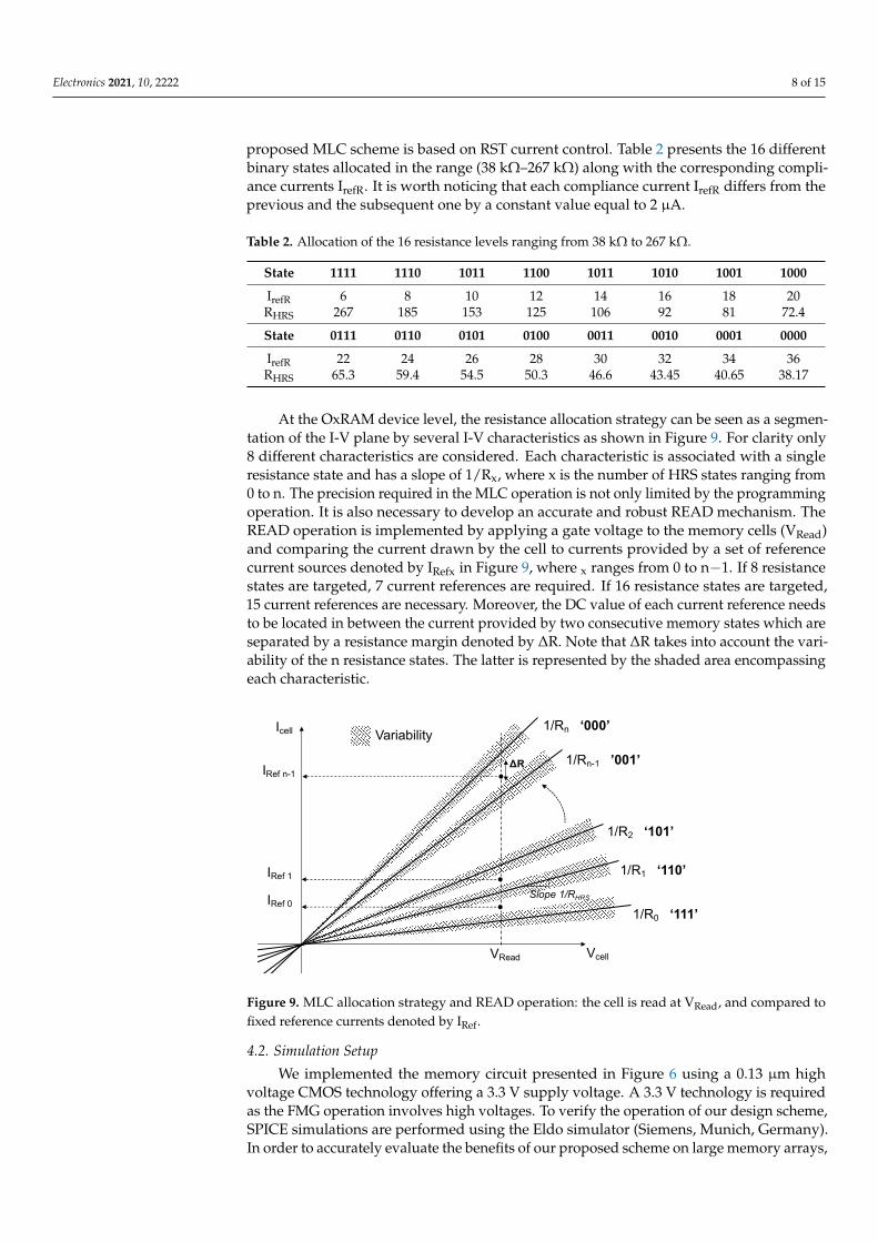
At the OxRAM device level, the resistance allocation strategy can be seen as a segmen-tation of the I-V plane by several I-V characteristics as shown in Figure 9. For clarity only8 different characteristics are considered. Each characteristic is associated with a singleresistance state and has a slope of 1/Rx, where x is the number of HRS states ranging from0 to n. The precision required in the MLC operation is not only limited by the programmingoperation. It is also necessary to develop an accurate and robust READ mechanism. TheREAD operation is implemented by applying a gate voltage to the memory cells (VRead)and comparing the current drawn by the cell to currents provided by a set of referencecurrent sources denoted by IRefx in Figure 9, where x ranges from 0 to n−1. If 8 resistancestates are targeted, 7 current references are required. If 16 resistance states are targeted,15 current references are necessary. Moreover, the DC value of each current reference needsto be located in between the current provided by two consecutive memory states which areseparated by a resistance margin denoted by ∆R. Note that ∆R takes into account the vari-ability of the n resistance states. The latter is represented by the shaded area encompassingeach characteristic.
Electronics 2021, 10, x FOR PEER REVIEW 8 of 15
∆R where the resistance is linearly spaced and ISO-∆I where the programming current (inverse of the resistance) is linearly spaced as described in [5]. The ISO-∆I approach is adopted as the proposed MLC scheme is based on RST current control. Table 2 presents the 16 different binary states allocated in the range (38 kΩ–267 kΩ) along with the corre-sponding compliance currents IrefR. It is worth noticing that each compliance current IrefR differs from the previous and the subsequent one by a constant value equal to 2 μA.
Table 2. Allocation of the 16 resistance levels ranging from 38 kΩ to 267 kΩ.
State 1111 1110 1011 1100 1011 1010 1001 1000 IrefR 6 8 10 12 14 16 18 20 RHRS 267 185 153 125 106 92 81 72.4 State 0111 0110 0101 0100 0011 0010 0001 0000 IrefR 22 24 26 28 30 32 34 36 RHRS 65.3 59.4 54.5 50.3 46.6 43.45 40.65 38.17
At the OxRAM device level, the resistance allocation strategy can be seen as a seg-mentation of the I-V plane by several I-V characteristics as shown in Figure 9. For clarity only 8 different characteristics are considered. Each characteristic is associated with a sin-gle resistance state and has a slope of 1/Rx, where x is the number of HRS states ranging from 0 to n. The precision required in the MLC operation is not only limited by the pro-gramming operation. It is also necessary to develop an accurate and robust READ mech-anism. The READ operation is implemented by applying a gate voltage to the memory cells (VRead) and comparing the current drawn by the cell to currents provided by a set of reference current sources denoted by IRefx in Figure 9, where x ranges from 0 to n−1. If 8 resistance states are targeted, 7 current references are required. If 16 resistance states are targeted, 15 current references are necessary. Moreover, the DC value of each current ref-erence needs to be located in between the current provided by two consecutive memory states which are separated by a resistance margin denoted by ΔR. Note that ΔR takes into account the variability of the n resistance states. The latter is represented by the shaded area encompassing each characteristic.
Figure 9. MLC allocation strategy and READ operation: the cell is read at VRead, and compared to fixed reference currents denoted by IRef.
4.2. Simulation Setup We implemented the memory circuit presented in Figure 6 using a 0.13 μm high volt-
age CMOS technology offering a 3.3 V supply voltage. A 3.3 V technology is required as the FMG operation involves high voltages. To verify the operation of our design scheme, SPICE simulations are performed using the Eldo simulator (Siemens, Munich, Germany). In order to accurately evaluate the benefits of our proposed scheme on large memory ar-rays, BL and WL lengths have been modelled to mimic a 1 Kbyte array (made of 1024 WLs
Icell
VRead Vcell
IRef 0
IRef 1
1/Rn-1 ’001’
1/R2 ‘101’
1/R1 ‘110’
1/R0 ‘111’
IRef n-1
1/Rn ‘000’
ΔR
Variability
Slope 1/RHRS
Figure 9. MLC allocation strategy and READ operation: the cell is read at VRead, and compared tofixed reference currents denoted by IRef.
4.2. Simulation Setup
We implemented the memory circuit presented in Figure 6 using a 0.13 µm highvoltage CMOS technology offering a 3.3 V supply voltage. A 3.3 V technology is requiredas the FMG operation involves high voltages. To verify the operation of our design scheme,SPICE simulations are performed using the Eldo simulator (Siemens, Munich, Germany).In order to accurately evaluate the benefits of our proposed scheme on large memory arrays,
Electronics 2021, 10, 2222 9 of 15
BL and WL lengths have been modelled to mimic a 1 Kbyte array (made of 1024 WLsand 1024 BLs). As a BL is characterized by a parasitic capacitance distributed through itslength, a 1 pF bit line capacitance is used according to the targeted technology and the arrayarchitecture. Additionally, parasitic resistances [24] distributed along BLs and WLs havebeen inserted in the design, following the methodology developed in [25]. Based on theproposed simulation setup, after SET, RST pulses with different compliance currents areapplied to the memory array. Then, HRS resistance values are extracted. More specifically,word programming is performed in two steps. Once an 8-bit word is addressed, eachmemory word is first entirely SET. Then a RST operation is performed in parallel throughthe SL with a predefined compliance current set according to the data bus values at the BLdriver level. During RST, multi-bit access is guaranteed as one RST write termination isassociated with a single bit-line (see Figure 7a,b).
4.3. Transient Simulations
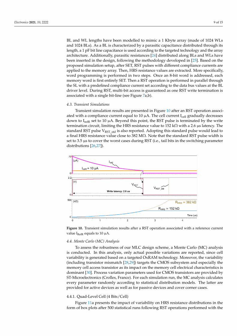
Transient simulation results are presented in Figure 10 after an RST operation associ-ated with a compliance current equal to 10 µA. The cell current Icell gradually decreasesdown to IrefR set to 10 µA. Beyond this point, the RST pulse is terminated by the writetermination circuit, limiting the HRS resistance value to 152 kΩ with a 2.6 µs latency. Thestandard RST pulse VRST_std is also reported. Adopting this standard pulse would lead toa final HRS resistance value close to 382 MΩ. Note that the standard RST pulse width isset to 3.5 µs to cover the worst cases during RST (i.e., tail bits in the switching parameterdistributions [26,27]).
Electronics 2021, 10, x FOR PEER REVIEW 9 of 15
and 1024 BLs). As a BL is characterized by a parasitic capacitance distributed through its length, a 1 pF bit line capacitance is used according to the targeted technology and the array architecture. Additionally, parasitic resistances [24] distributed along BLs and WLs have been inserted in the design, following the methodology developed in [25]. Based on the proposed simulation setup, after SET, RST pulses with different compliance currents are applied to the memory array. Then, HRS resistance values are extracted. More specif-ically, word programming is performed in two steps. Once an 8-bit word is addressed, each memory word is first entirely SET. Then a RST operation is performed in parallel through the SL with a predefined compliance current set according to the data bus values at the BL driver level. During RST, multi-bit access is guaranteed as one RST write termi-nation is associated with a single bit-line (see Figure 7a,b).
4.3. Transient Simulations Transient simulation results are presented in Figure 10 after an RST operation asso-
ciated with a compliance current equal to 10 μA. The cell current Icell gradually decreases down to IrefR set to 10 μA. Beyond this point, the RST pulse is terminated by the write termination circuit, limiting the HRS resistance value to 152 kΩ with a 2.6 μs latency. The standard RST pulse VRST_std is also reported. Adopting this standard pulse would lead to a final HRS resistance value close to 382 MΩ. Note that the standard RST pulse width is set to 3.5 μs to cover the worst cases during RST (i.e., tail bits in the switching parameter distributions [26,27]).
Figure 10. Transient simulation results after a RST operation associated with a reference current value IRefR equals to 10 μA.
4.4. Monte Carlo (MC) Analysis To assess the robustness of our MLC design scheme, a Monte Carlo (MC) analysis is
conducted. In this analysis, only actual possible variations are reported, since cell varia-bility is generated based on a targeted OxRAM technology. Moreover, the variability (in-cluding transistor mismatch [28,29]) targets the CMOS subsystem and especially the memory cell access transistor as its impact on the memory cell electrical characteristics is dominant [30]. Process variation parameters used for CMOS transistors are provided by ST-Microelectronics (Crolles, France). For each simulation run, the MC analysis calculates every parameter randomly according to statistical distribution models. The latter are pro-vided for active devices as well as for passive devices and cover corner cases.
4.4.1. Quad-Level Cell (4 Bits/Cell) Figure 11a presents the impact of variability on HRS resistance distributions in the
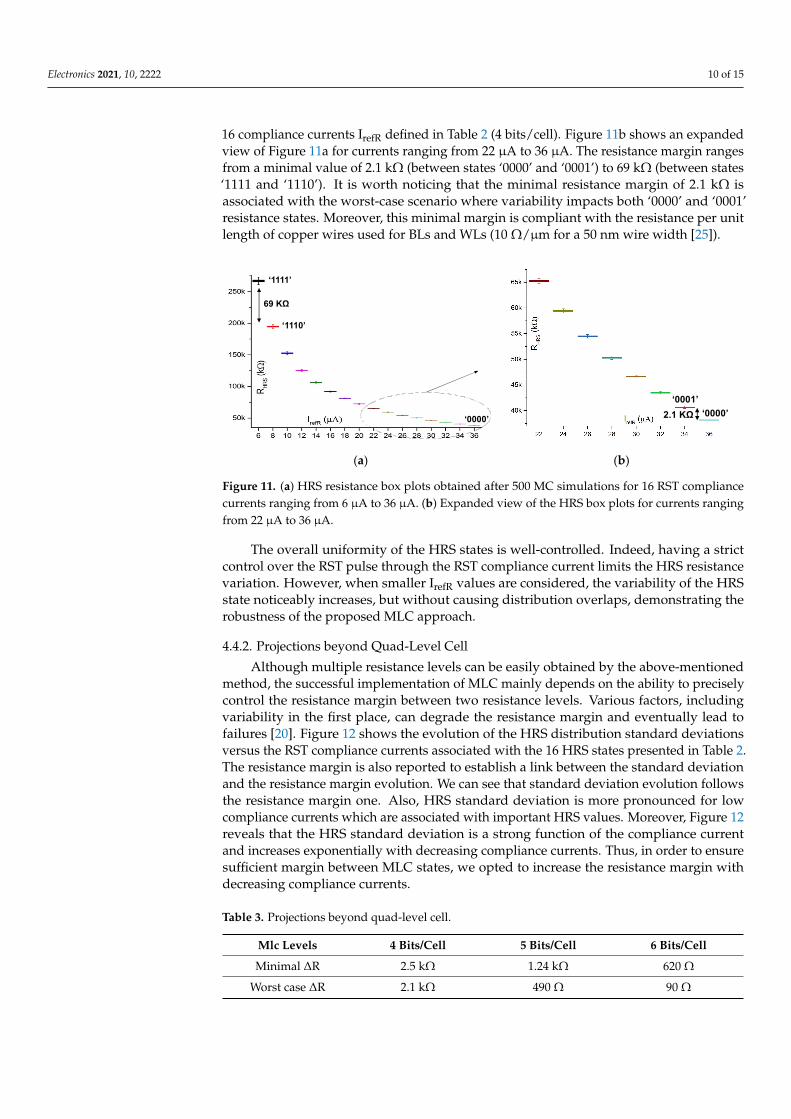
form of box plots after 500 statistical runs following RST operations performed with the 16 compliance currents IrefR defined in Table 2 (4 bits/cell). Figure 11b shows an expanded view of Figure 11a for currents ranging from 22 μA to 36 μA. The resistance margin ranges from a minimal value of 2.1 kΩ (between states ‘0000’ and ‘0001’) to 69 kΩ (between states
Figure 10. Transient simulation results after a RST operation associated with a reference currentvalue IRefR equals to 10 µA.
4.4. Monte Carlo (MC) Analysis
To assess the robustness of our MLC design scheme, a Monte Carlo (MC) analysisis conducted. In this analysis, only actual possible variations are reported, since cellvariability is generated based on a targeted OxRAM technology. Moreover, the variability(including transistor mismatch [28,29]) targets the CMOS subsystem and especially thememory cell access transistor as its impact on the memory cell electrical characteristics isdominant [30]. Process variation parameters used for CMOS transistors are provided byST-Microelectronics (Crolles, France). For each simulation run, the MC analysis calculatesevery parameter randomly according to statistical distribution models. The latter areprovided for active devices as well as for passive devices and cover corner cases.
4.4.1. Quad-Level Cell (4 Bits/Cell)
Figure 11a presents the impact of variability on HRS resistance distributions in theform of box plots after 500 statistical runs following RST operations performed with the
Electronics 2021, 10, 2222 10 of 15
16 compliance currents IrefR defined in Table 2 (4 bits/cell). Figure 11b shows an expandedview of Figure 11a for currents ranging from 22 µA to 36 µA. The resistance margin rangesfrom a minimal value of 2.1 kΩ (between states ‘0000’ and ‘0001’) to 69 kΩ (between states‘1111 and ‘1110’). It is worth noticing that the minimal resistance margin of 2.1 kΩ isassociated with the worst-case scenario where variability impacts both ‘0000’ and ‘0001’resistance states. Moreover, this minimal margin is compliant with the resistance per unitlength of copper wires used for BLs and WLs (10 Ω/µm for a 50 nm wire width [25]).
Electronics 2021, 10, x FOR PEER REVIEW 10 of 15
‘1111 and ‘1110’). It is worth noticing that the minimal resistance margin of 2.1 kΩ is as-sociated with the worst-case scenario where variability impacts both ‘0000’ and ‘0001’ re-sistance states. Moreover, this minimal margin is compliant with the resistance per unit length of copper wires used for BLs and WLs (10 Ω/μm for a 50 nm wire width [25]).
The overall uniformity of the HRS states is well-controlled. Indeed, having a strict control over the RST pulse through the RST compliance current limits the HRS resistance variation. However, when smaller IrefR values are considered, the variability of the HRS state noticeably increases, but without causing distribution overlaps, demonstrating the robustness of the proposed MLC approach.
(a) (b)
Figure 11. (a) HRS resistance box plots obtained after 500 MC simulations for 16 RST compliance currents ranging from 6 μA to 36 μA. (b) Expanded view of the HRS box plots for currents ranging from 22 μA to 36 μA.
4.4.2. Projections beyond Quad-Level Cell Although multiple resistance levels can be easily obtained by the above-mentioned
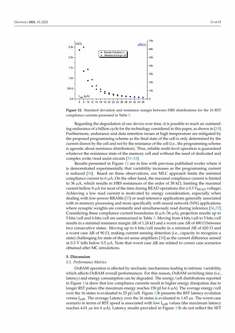
method, the successful implementation of MLC mainly depends on the ability to precisely control the resistance margin between two resistance levels. Various factors, including variability in the first place, can degrade the resistance margin and eventually lead to fail-ures [20]. Figure 12 shows the evolution of the HRS distribution standard deviations ver-sus the RST compliance currents associated with the 16 HRS states presented in Table 2. The resistance margin is also reported to establish a link between the standard deviation and the resistance margin evolution. We can see that standard deviation evolution follows the resistance margin one. Also, HRS standard deviation is more pronounced for low com-pliance currents which are associated with important HRS values. Moreover, Figure 12 reveals that the HRS standard deviation is a strong function of the compliance current and increases exponentially with decreasing compliance currents. Thus, in order to ensure suf-ficient margin between MLC states, we opted to increase the resistance margin with de-creasing compliance currents.
Regarding the degradation of our device over time, it is possible to reach an out-standing endurance of a billion cycle for the technology considered in this paper, as shown in [19]. Furthermore, endurance and data retention issues at high temperature are miti-gated by the proposed programming scheme as the final state of the cell is only deter-mined by the current drawn by the cell and not by the resistance of the cell (i.e., the pro-gramming scheme is agnostic about resistance distribution). Thus, reliable multi-level op-eration is guaranteed whatever the resistance state of the memory cell and without the need of dedicated and complex write/read assist circuits [31–33].
69 KΩ
‘0000’
‘1111’
‘1110’
2.1 KΩ ‘0000’‘0001’
Figure 11. (a) HRS resistance box plots obtained after 500 MC simulations for 16 RST compliancecurrents ranging from 6 µA to 36 µA. (b) Expanded view of the HRS box plots for currents rangingfrom 22 µA to 36 µA.
The overall uniformity of the HRS states is well-controlled. Indeed, having a strictcontrol over the RST pulse through the RST compliance current limits the HRS resistancevariation. However, when smaller IrefR values are considered, the variability of the HRSstate noticeably increases, but without causing distribution overlaps, demonstrating therobustness of the proposed MLC approach.
4.4.2. Projections beyond Quad-Level Cell
Although multiple resistance levels can be easily obtained by the above-mentionedmethod, the successful implementation of MLC mainly depends on the ability to preciselycontrol the resistance margin between two resistance levels. Various factors, includingvariability in the first place, can degrade the resistance margin and eventually lead tofailures [20]. Figure 12 shows the evolution of the HRS distribution standard deviationsversus the RST compliance currents associated with the 16 HRS states presented in Table 2.The resistance margin is also reported to establish a link between the standard deviationand the resistance margin evolution. We can see that standard deviation evolution followsthe resistance margin one. Also, HRS standard deviation is more pronounced for lowcompliance currents which are associated with important HRS values. Moreover, Figure 12reveals that the HRS standard deviation is a strong function of the compliance currentand increases exponentially with decreasing compliance currents. Thus, in order to ensuresufficient margin between MLC states, we opted to increase the resistance margin withdecreasing compliance currents.
Table 3. Projections beyond quad-level cell.
Mlc Levels 4 Bits/Cell 5 Bits/Cell 6 Bits/Cell
Minimal ∆R 2.5 kΩ 1.24 kΩ 620 Ω
Worst case ∆R 2.1 kΩ 490 Ω 90 Ω
Electronics 2021, 10, 2222 11 of 15Electronics 2021, 10, x FOR PEER REVIEW 11 of 15
Figure 12. Standard deviation and resistance margin between HRS distributions for the 16 RST com-pliance currents presented in Table 3.
Results presented in Figure 12 are in line with previous published works where it is demonstrated experimentally that variability increases as the programming current is re-duced [34]. Based on these observations, our MLC approach limits the minimal compli-ance current to 6 μA. On the other hand, the maximal compliance current is limited to 36 μA, which results in HRS resistances of the order of 38 kΩ, limiting the maximal current bellow 8 μA for most of the time during READ operations (for a 0.3 VREAD voltage). Achiev-ing a low read current is motivated by energy consideration, especially when dealing with low-power RRAMs [35] or read-intensive applications generally associated with in-memory processing and more specifically with neural network (NN) applications where synaptic weights are constantly and simultaneously read during inference [36,37]. Con-sidering these compliance current boundaries (6 μA–36 μA), projection results up to 5 bits/cell and 6 bits/cell are summarized in Table 3. Moving from 4 bits/cell to 5 bits/cell results in a minimal resistance margin ∆R of 1.24 kΩ and a worst case ∆R of 490 Ω between two consecutive states. Moving up to 6 bits/cell results in a minimal ∆R of 620 Ω and a worst case ∆R of 90 Ω, making current sensing detection (i.e., capacity to recognize a state) challenging for state-of-the-art sense amplifiers [38] as the current difference sensed at 0.3 V falls below 0.5 μA. Note that worst case ∆R are related to corner case scenarios obtained after MC simulations.
Table 3. Projections beyond quad-level cell.
Mlc Levels 4 Bits/Cell 5 Bits/Cell 6 Bits/Cell Minimal ∆R 2.5 kΩ 1.24 kΩ 620 Ω
Worst case ∆R 2.1 kΩ 490 Ω 90 Ω
5. Discussion 5.1. Performance Metrics
OxRAM operation is affected by stochastic mechanisms leading to intrinsic variabil-ity, which affects OxRAM overall performances. For this reason, OxRAM switching time (i.e., latency) and energy consumption can be degraded. The energy/cell distributions re-ported in Figure 13a show that low compliance currents result in higher energy dissipa-tion due to longer RST pulses (the maximum energy reaches 150 pJ for 6 μA). The average energy/cell over the 16 states is evaluated to 25 pJ/cell. Figure 13b presents the RST latency evolution versus IrefR. The average Latency over the 16 states is evaluated to 1.65 μs. The worst-case scenario in terms of RST speed is associated with low IrefR values (the maximum latency reaches 4.01 μs for 6 μA). Latency results provided in Figure 13b do not reflect the SET operation preceding each RST operation. This is explained by the fact that the
Figure 12. Standard deviation and resistance margin between HRS distributions for the 16 RSTcompliance currents presented in Table 3.
Regarding the degradation of our device over time, it is possible to reach an outstand-ing endurance of a billion cycle for the technology considered in this paper, as shown in [19].Furthermore, endurance and data retention issues at high temperature are mitigated bythe proposed programming scheme as the final state of the cell is only determined by thecurrent drawn by the cell and not by the resistance of the cell (i.e., the programming schemeis agnostic about resistance distribution). Thus, reliable multi-level operation is guaranteedwhatever the resistance state of the memory cell and without the need of dedicated andcomplex write/read assist circuits [31–33].
Results presented in Figure 12 are in line with previous published works where itis demonstrated experimentally that variability increases as the programming currentis reduced [34]. Based on these observations, our MLC approach limits the minimalcompliance current to 6 µA. On the other hand, the maximal compliance current is limitedto 36 µA, which results in HRS resistances of the order of 38 kΩ, limiting the maximalcurrent bellow 8 µA for most of the time during READ operations (for a 0.3 VREAD voltage).Achieving a low read current is motivated by energy consideration, especially whendealing with low-power RRAMs [35] or read-intensive applications generally associatedwith in-memory processing and more specifically with neural network (NN) applicationswhere synaptic weights are constantly and simultaneously read during inference [36,37].Considering these compliance current boundaries (6 µA–36 µA), projection results up to5 bits/cell and 6 bits/cell are summarized in Table 3. Moving from 4 bits/cell to 5 bits/cellresults in a minimal resistance margin ∆R of 1.24 kΩ and a worst case ∆R of 490 Ω betweentwo consecutive states. Moving up to 6 bits/cell results in a minimal ∆R of 620 Ω anda worst case ∆R of 90 Ω, making current sensing detection (i.e., capacity to recognize astate) challenging for state-of-the-art sense amplifiers [38] as the current difference sensedat 0.3 V falls below 0.5 µA. Note that worst case ∆R are related to corner case scenariosobtained after MC simulations.
5. Discussion5.1. Performance Metrics
OxRAM operation is affected by stochastic mechanisms leading to intrinsic variability,which affects OxRAM overall performances. For this reason, OxRAM switching time (i.e.,latency) and energy consumption can be degraded. The energy/cell distributions reportedin Figure 13a show that low compliance currents result in higher energy dissipation due tolonger RST pulses (the maximum energy reaches 150 pJ for 6 µA). The average energy/cellover the 16 states is evaluated to 25 pJ/cell. Figure 13b presents the RST latency evolutionversus IrefR. The average Latency over the 16 states is evaluated to 1.65 µs. The worst-casescenario in terms of RST speed is associated with low IrefR values (the maximum latencyreaches 4.01 µs for 6 µA). Latency results provided in Figure 13b do not reflect the SET

Electronics 2021, 10, 2222 12 of 15
operation preceding each RST operation. This is explained by the fact that the standard SETpulse is constant and common to any RST operation. The SET pulse is very short (~100 ns),which is a common feature of the considered OxRAM technology and contributes 20 pJ/cellto the total energy dissipation. Hence, in the worst case, the total energy/cell associatedwith a SET/RST cycle can reach 175 pJ.
Electronics 2021, 10, x FOR PEER REVIEW 12 of 15
standard SET pulse is constant and common to any RST operation. The SET pulse is very short (~100 ns), which is a common feature of the considered OxRAM technology and contributes 20 pJ/cell to the total energy dissipation. Hence, in the worst case, the total energy/cell associated with a SET/RST cycle can reach 175 pJ.
(a) (b)
Figure 13. (a) Energy/cell and (b) RST latency box plots obtained after 500 MC simulation performed for RST compliance currents ranging from 6 μA to 36 μA (4 bits/cell).
5.2. Comparison with State-of-the-Art MLC Approaches Table 4 summarizes the proposed MLC design scheme and compares it to the state-
of-the-art. Comparison metrics include the targeted RRAM technology, the number of re-sistance states, the MLC operation mode and the design level (i.e., device or circuit level). Storing 8 states has been reported in [12,14,39,40] at the device level, mainly by varying RST voltages (VRST) and programming pulses. Our methodology is the first one to report 16 HRS resistance levels, which is a major step forward compared to the state-of-the-art. The approach leveraging on compliance current (IC) control in the RST direction, pro-posed in [14], is extended to 4 bits/cell. The only approach implemented at the circuit level is developed in [17]. However, this approach only considers the read operation of MLC RRAMs where the current drawn from a 2 bits/cell RRAM is converted to voltage pulses proportional to the current’s magnitude of the cell. No mention of MLC programming is made.
Table 4. Projections beyond quad-level cell.
RRAM Device States
Number MLC Mode Design Level
[8] Pt/TaOx/Ta2O5/Pt 4 HRS VRST Device [11] TiN/HfTiO2/TiN 3 LRS/1 HRS IC SET Device [39] TiN/HfOx/Pt 8 HRS VRST Device [13] Cu/HfO2/Cu/Pt 3 LRS/1 HRS IC SET Device [17] Ti/HfOx/Ti/TiN 3 LRS/1 HRS IC SET Circuit [12] TiN/HfOx/Pt 8 HRS VRST Device [40] Pt/W/ TaOx / Pt 7 HRS/1 LRS VRST Device [14] TiN/Ti/HfOx/TiN 8 HRS IC RST Circuit
Work TiN/Ti/HfOx/TiN 16 HRS IC RST Circuit
6. Conclusions MLC RRAM research is still in an early stage and most studies are focused on the
device level. In this context, an MLC operation design scheme based on RST current con-trol is proposed at the circuit level to achieve robust MLC operation without the need of read-verify operations. The proposed write termination circuit allows remarkable re-sistance margins between consecutive memory states. Quad-level cell with 4 bits/cell
Figure 13. (a) Energy/cell and (b) RST latency box plots obtained after 500 MC simulation performedfor RST compliance currents ranging from 6 µA to 36 µA (4 bits/cell).
5.2. Comparison with State-of-the-Art MLC Approaches
Table 4 summarizes the proposed MLC design scheme and compares it to the state-of-the-art. Comparison metrics include the targeted RRAM technology, the number ofresistance states, the MLC operation mode and the design level (i.e., device or circuit level).Storing 8 states has been reported in [12,14,39,40] at the device level, mainly by varyingRST voltages (VRST) and programming pulses. Our methodology is the first one to report16 HRS resistance levels, which is a major step forward compared to the state-of-the-art.The approach leveraging on compliance current (IC) control in the RST direction, proposedin [14], is extended to 4 bits/cell. The only approach implemented at the circuit level isdeveloped in [17]. However, this approach only considers the read operation of MLCRRAMs where the current drawn from a 2 bits/cell RRAM is converted to voltage pulsesproportional to the current’s magnitude of the cell. No mention of MLC programmingis made.
Table 4. Projections beyond quad-level cell.
RRAM Device States Number MLC Mode Design Level
[8] Pt/TaOx/Ta2O5/Pt 4 HRS VRST Device[11] TiN/HfTiO2/TiN 3 LRS/1 HRS IC SET Device[39] TiN/HfOx/Pt 8 HRS VRST Device[13] Cu/HfO2/Cu/Pt 3 LRS/1 HRS IC SET Device[17] Ti/HfOx/Ti/TiN 3 LRS/1 HRS IC SET Circuit[12] TiN/HfOx/Pt 8 HRS VRST Device[40] Pt/W/ TaOx/Pt 7 HRS/1 LRS VRST Device[14] TiN/Ti/HfOx/TiN 8 HRS IC RST Circuit
Work TiN/Ti/HfOx/TiN 16 HRS IC RST Circuit
6. Conclusions
MLC RRAM research is still in an early stage and most studies are focused on thedevice level. In this context, an MLC operation design scheme based on RST current controlis proposed at the circuit level to achieve robust MLC operation without the need of read-verify operations. The proposed write termination circuit allows remarkable resistancemargins between consecutive memory states. Quad-level cell with 4 bits/cell simulationresults are presented to validate the concept. Simulation results are validated versus vari-ability to assess the robustness of the proposed MLC scheme. For the proposed 4 bits/cell
Electronics 2021, 10, 2222 13 of 15
approach, resistance margins are extracted and the worst-case margin reaches 2.1 kΩ.Moreover, the proposed MLC approach is flexible as it can target different HRS resistanceranges to optimize both energy and latency. Extensions of the current work will addressthe application of the presented MLC design scheme to any resistive RAM technology,providing an analog programming mechanism, such as phase-change memory (PCM).
Author Contributions: Conceptualization, H.A., M.M., M.F. and S.H.; formal analysis, H.A., A.V.,M.T. and P.G.; methodology, H.A.; project administration, H.A.; supervision, H.A.; writing–originaldraft, H.A. and S.H.; writing–review and editing, M.F, P.G., A.V., M.M., K.C. and H.A. All authorshave read and agreed to the published version of the manuscript.
Funding: This research received no external funding.
Institutional Review Board Statement: Not applicable.
Informed Consent Statement: Not applicable.
Data Availability Statement: Not applicable.
Conflicts of Interest: The authors declare no conflict of interest.
References1. Aziza, H. Embedded Memories. In Silicon Systems for Wireless Lan; Stamenkovic, Z., Leger, G., Bosio, A., Eds.; World Scientific:
Singapore, 2020; Volume 22, pp. 199–222. [CrossRef]2. Lee, Y.-L.; Tsung, P.-K.; Wu, M. Techology trend of edge AI. In Proceedings of the 2018 International Symposium on VLSI Design,
Automation and Test (VLSI-DAT), Hsinchu, Taiwan, 16–19 April 2018; pp. 1–2. [CrossRef]3. Yu, S.; Chen, P.-Y. Emerging Memory Technologies: Recent Trends and Prospects. IEEE Solid-State Circuits Mag. 2016, 8, 43–56.
[CrossRef]4. Ielmini, D. Resistive switching memories based on metal oxides: Mechanisms, reliability and scaling. Semicond. Sci. Technol. 2016,
31, 063002. [CrossRef]5. Xu, C.; Niu, D.; Muralimanohar, N.; Jouppi, N.P.; Xie, Y. Understanding the trade-offs in multi-level cell ReRAM memory design.
In Proceedings of the 50th Annual Design Automation Conference, Austin, TX, USA, 29 May–7 June 2013; p. 108. [CrossRef]6. Liang, J.; Wong, H.-S.P. Cross-Point Memory Array without Cell Selectors—Device Characteristics and Data Storage Pattern
Dependencies. IEEE Trans. Electron Devices 2010, 57, 2531–2538. [CrossRef]7. Gao, R.; Lei, D.; He, Z.; En, Y.; Huang, Y. Layer-dependent resistance variability assessment on 2048 8-layer 3D vertical RRAMs.
Electron. Lett. 2019, 55, 955–957. [CrossRef]8. Lee, S.R.; Kim, Y.-B.; Chang, M.; Kim, K.M.; Lee, C.B.; Hur, J.H.; Park, G.-S.; Lee, D.; Lee, M.-J.; Kim, C.J.; et al. Multi-level
switching of triple-layered TaOx RRAM with excellent reliability for storage class memory. In Proceedings of the 2012 Symposiumon VLSI Technology (VLSIT), Honolulu, HI, USA, 12–14 June 2012; pp. 71–72. [CrossRef]
9. Lee, M.-H.; Lin, Y.-H.; Lee, F.-M.; Lee, D.-Y.; Hsieh, K.-Y. Studies on ReRAM Conduction Mechanism and the Varying-bias ReadScheme for MLC and Wide Temperature Range TMO ReRAM. In Proceedings of the 14th IEEE International Conference onSolid-State and Integrated Circuit Technology (ICSICT), Qingdao, China, 31 October–3 November 2018; pp. 1–3. [CrossRef]
10. Zhu, X.; Su, W.; Liu, Y.; Hu, B.; Pan, L.; Lu, W.; Zhang, J.; Li, R.-W. Observation of Conductance Quantization in Oxide-BasedResistive Switching Memory. Adv. Mater. 2012, 24, 3941–3946. [CrossRef] [PubMed]
11. Chakrabarti, B.; Galatage, R.V.; Vogel, E.M. Multilevel Switching in Forming-Free Resistive Memory Devices with Atomic LayerDeposited HfTiOx Nanolaminate. IEEE Electron Device Lett. 2013, 34, 867–869. [CrossRef]
12. Zhao, L.; Chen, H.-Y.; Wu, S.-C.; Jiang, Z.; Yu, S.; Hou, T.-H.; Wong, H.-S.P.; Nishi, Y.; Shimeng, Y. Improved multi-level controlof RRAM using pulse-train programming. In Proceedings of the Technical Program—2014 International Symposium on VLSITechnology, Systems and Application (VLSI-TSA), Hsinchu, Taiwan, 28–30 April 2014; pp. 1–2. [CrossRef]
13. Wang, Y.; Liu, Q.; Long, S.; Wang, W.; Wang, Q.; Zhang, M.; Zhang, S.; Li, Y.; Zuo, Q.; Yang, J.; et al. Investigation of resistiveswitching in Cu-doped HfO2thin film for multilevel non-volatile memory applications. Nanotechnol. 2009, 21, 045202. [CrossRef]
14. Aziza, H.; Hamdioui, S.; Fieback, M.; Taouil, M.; Moreau, M. Density Enhancement of RRAMs using a RESET Write Terminationfor MLC Operation. In Proceedings of the Design, Automation & Test in Europe Conference & Exhibition (DATE), Grenoble,France, 1–5 February 2021; pp. 1877–1880. [CrossRef]
15. Zangeneh, M.; Joshi, A. Design and Optimization of Nonvolatile Multibit 1T1R Resistive RAM. IEEE Trans. Very Large Scale Integr.(VLSI) Syst. 2013, 22, 1815–1828. [CrossRef]
16. Xing, J.; Xu, H.; Li, J.; Wang, W.; Liu, H.; Li, Q. Practical considerations of read-out circuits for passive, multi-level ReRAM arrays.In Proceedings of the 2016 IEEE International Conference on Manipulation, Manufacturing and Measurement on the Nanoscale(3M-NANO), Chongqing, China, 18–22 July 2016; pp. 168–171. [CrossRef]
Electronics 2021, 10, 2222 14 of 15
17. Reuben, J.; Fey, D. A Time-based Sensing Scheme for Multi-level Cell (MLC) Resistive RAM. In Proceedings of the IEEE NordicCircuits and Systems Conference (NORCAS): NORCHIP and International Symposium of System-on-Chip (SoC), Helsinki,Finland, 29–30 October 2019; pp. 1–6. [CrossRef]
18. Zahoor, F.; Zulkifli, T.Z.A.; Khanday, F.A. Resistive Random Access Memory (RRAM): An Overview of Materials, SwitchingMechanism, Performance, Multilevel Cell (mlc) Storage, Modeling, and Applications. Nanoscale Res. Lett. 2020, 15, 1–26.[CrossRef]
19. Barlas, M.; Grossi, A.; Grenouillet, L.; Vianello, E.; Nolot, E.; Vaxelaire, N.; Blaise, P.; Traore, B.; Coignus, J.; Perrin, F.; et al.Improvement of HfO2 based RRAM array performances by local Si implantation. In Proceedings of the IEEE InternationalElectron Devices Meeting (IEDM), San Francisco, CA, USA, 2–6 December 2017; pp. 14.6.1–14.6.4. [CrossRef]
20. Grossi, A.; Nowak, E.; Zambelli, C.; Pellissier, C.; Bernasconi, S.; Cibrario, G.; El Hajjam, K.; Crochemore, R.; Nodin, J.; Olivo, P.;et al. Fundamental variability limits of filament-based RRAM. In Proceedings of the IEEE International Electron Devices Meeting(IEDM), San Francisco, CA, USA, 3–7 December 2016; pp. 4.7.1–4.7.4.
21. Bocquet, M.; Aziza, H.; Zhao, W.; Zhang, Y.; Onkaraiah, S.; Muller, C.; Reyboz, M.; Deleruyelle, D.; Clermidy, F.; Portal, J.-M.Compact Modeling Solutions for Oxide-Based Resistive Switching Memories (OxRAM). J. Low Power Electron. Appl. 2014, 4, 1–14.[CrossRef]
22. Hajri, B.; Mansour, M.M.; Chehab, A.; Aziza, H. Oxide-based RRAM models for circuit designers: A comparative analysis.In Proceedings of the 12th International Conference on Design & Technology of Integrated Systems in Nanoscale Era (DTIS),Palma de Mallorca, Spain, 4–6 April 2017; pp. 1–6. [CrossRef]
23. Banba, H.; Shiga, H.; Umezawa, A.; Miyaba, T.; Tanzawa, T.; Atsumi, S.; Sakui, K. A CMOS bandgap reference circuit withsub-1-V operation. IEEE J. Solid-state Circuits 1999, 34, 670–674. [CrossRef]
24. Aziza, H.; Canet, P.; Postel-Pellerin, J.; Moreau, M.; Portal, J.-M.; Bocquet, M. ReRAM ON/OFF resistance ratio degradation due toline resistance combined with device variability in 28 nm FDSOI technology. In Proceedings of the Joint International EUROSOIWorkshop and International Conference on Ultimate Integration on Silicon (EUROSOI-ULIS), Athens, Greece, 3–5 April 2017;pp. 35–38. [CrossRef]
25. Liang, J.; Yeh, S.; Wong, S.S.; Wong, H.-S.P. Effect of Wordline/Bitline Scaling on the Performance, Energy Consumption, andReliability of Cross-Point Memory Array. ACM J. Emerg. Technol. Comput. Syst. 2013, 9, 1–14. [CrossRef]
26. Aziza, H.; Moreau, M.; Fieback, M.; Taouil, M.; Hamdioui, S. An Energy-Efficient Current-Controlled Write and Read Scheme forResistive RAMs (RRAMs). IEEE Access 2020, 8, 137263–137274. [CrossRef]
27. Hajri, B.; Aziza, H.; Mansour, M.M.; Chehab, A. RRAM Device Models: A Comparative Analysis with Experimental Validation.IEEE Access 2019, 7, 168963–168980. [CrossRef]
28. Joly, Y.; Lopez, L.; Portal, J.-M.; Aziza, H.; Bert, Y.; Julien, F.; Fornara, P. Impact of hump effect on MOSFET mismatch in thesub-threshold area for low power analog applications. In Proceedings of the 10th IEEE International Conference on Solid-Stateand Integrated Circuit Technology, Shanghai, China, 1–4 November 2010; pp. 1817–1819. [CrossRef]
29. Joly, Y.; Lopez, L.; Truphemus, L.; Portal, J.-M.; Aziza, H.; Julien, F.; Fornara, P.; Masson, P.; Ogier, J.-L.; Bert, Y. Gate VoltageMatching Investigation for Low-Power Analog Applications. IEEE Trans. Electron. Devices 2013, 60, 1263–1267. [CrossRef]
30. Aziza, H.; Bocquet, M.; Portal, J.-M.; Muller, C. Evaluation of OxRAM cell variability impact on memory performances throughelectrical simulations. In Proceedings of the 11th Annual Non-Volatile Memory Technology Symposium Proceeding, Shanghai,China, 7–9 November 2011. [CrossRef]
31. Xue, X.; Jian, W.; Yang, J.; Xiao, F.; Chen, G.; Xu, S.; Xie, Y.; Lin, Y.; Huang, R.; Zou, Q.; et al. A 0.13 µm 8 Mb Logic-BasedCuxSiyO ReRAM with Self-Adaptive Operation for Yield Enhancement and Power Reduction. IEEE J. Solid-State Circuits 2013, 48,1315–1322. [CrossRef]
32. Chen, W.-H.; Lin, W.-J.; Lai, L.-Y.; Li, S.; Hsu, C.-H.; Lin, H.-T.; Lee, H.-Y.; Su, J.-W.; Xie, Y.; Sheu, S.-S.; et al. A 16Mb dual-mode ReRAM macro with sub-14ns computing-in-memory and memory functions enabled by self-write termination scheme.In Proceedings of the IEEE International Electron Devices Meeting (IEDM), San Francisco, CA, USA, 2–6 December 2017;pp. 657–660. [CrossRef]
33. Chang, M.-F.; Wu, J.-J.; Chien, T.-F.; Liu, Y.-C.; Yang, T.-C.; Shen, W.-C.; King, Y.-C.; Lin, C.J.; Lin, K.-F.; Chih, Y.-D.; et al. LowVDDmin Swing-Sample-and-Couple Sense Amplifier and Energy-Efficient Self-Boost-Write-Termination Scheme for EmbeddedReRAM Macros Against Resistance and Switch-Time Variations. IEEE J. Solid-State Circuits 2015, 50, 2786–2795. [CrossRef]
34. Aziza, H.; Postel-Pellerin, J.; Bazzi, H.; Canet, P.; Moreau, M.; Della Marca, V.; Harb, A. True Random Number GeneratorIntegration in a Resistive RAM Memory Array Using Input Current Limitation. IEEE Trans. Nanotechnol. 2020, 19, 214–222.[CrossRef]
35. Portal, J.-M.; Bocquet, M.; Onkaraiah, S.; Moreau, M.; Aziza, H.; Deleruyelle, D.; Torki, K.; Vianello, E.; Levisse, A.; Giraud, B.;et al. Design and Simulation of a 128 kb Embedded Nonvolatile Memory Based on a Hybrid RRAM (HfO2)/28 nm FDSOI CMOSTechnology. IEEE Trans. Nanotechnol. 2017, 16, 677–686. [CrossRef]
36. Vaz, P.I.; Girard, P.; Virazel, A.; Aziza, H. Improving TID Radiation Robustness of a CMOS OxRAM-Based Neuron Circuit byUsing Enclosed Layout Transistors. IEEE Trans. Very Large Scale Integr. (VLSI) Syst. 2021, 29, 1122–1131. [CrossRef]
37. Aziza, H.; Moreau, M.; Perez, A.; Virazel, A.; Girard, P. A Capacitor-Less CMOS Neuron Circuit for Neuromemristive Networks.In Proceedings of the 17th IEEE International New Circuits and Systems Conference (NEWCAS), Munich Germany, 23–26 June2019; pp. 1–4. [CrossRef]

Electronics 2021, 10, 2222 15 of 15
38. Na, T.; Song, B.; Kim, J.P.; Kang, S.H.; Jung, S.-O. Offset-Canceling Current-Sampling Sense Amplifier for Resistive NonvolatileMemory in 65 nm CMOS. IEEE J. Solid-State Circuits 2017, 52, 496–504. [CrossRef]
39. Zhao, L.; Chen, H.-Y.; Wu, S.-C.; Jiang, Z.; Yu, S.; Hou, T.-H.; Wong, H.-S.P.; Nishi, Y. Multi-level control of conductivenano-filament evolution in HfO2 ReRAM by pulse-train operations. Nanoscale 2014, 6, 5698–5702. [CrossRef] [PubMed]
40. Kim, W.; Menzel, S.; Wouters, D.J.; Waser, R.; Rana, V. 3-Bit Multilevel Switching by Deep Reset Phenomenon in Pt/W/TaOX/Pt-ReRAM Devices. IEEE Electron. Device Lett. 2016, 37, 564–567. [CrossRef]
![Graphene and Related Materials for Resistive Random Access ... · PDF fileGraphene and Related Materials for Resistive Random Access Memories ... magnetoresistive RAM (MRAM),[17,18]](https://img.pdfslide.us/doc/110x75/5aa8d81e7f8b9a90188c1063/graphene-and-related-materials-for-resistive-random-access-and-related-materials.jpg)