Embed Size (px)
Citation preview
© imec 2013
Resistive RAM based Memory Hierarchy for Ultra-low Power
Data-parallel Processor Platform Francky Catthoor
With use of MSc and PhD thesis results in cooperation with ReRAM team at IMEC Also based on ULP-DSIP PhD team work

© imec 2013 IMEC confidential
Secure, trustworthy computing and communication embedded in every-thing and every-body.
A pervasive, context aware ambient, sensitive and responsive to the presence of people
Ambient intelligence

© imec 2013 IMEC confidential
Personal Healthcare Vision
EEG
Hearing
ECG
Blood Pressure
Toxins
glucose
Implants
Vision
DNA protein
positioning
Cellular
POTS
WLAN
Net
wor
k

© imec 2013
Connected Everywhere Vision
Connectivity to Server
Interaction with sensor network
Teleconference
and much more?
Wireless Terminal
Other Terminals
© imec 2013
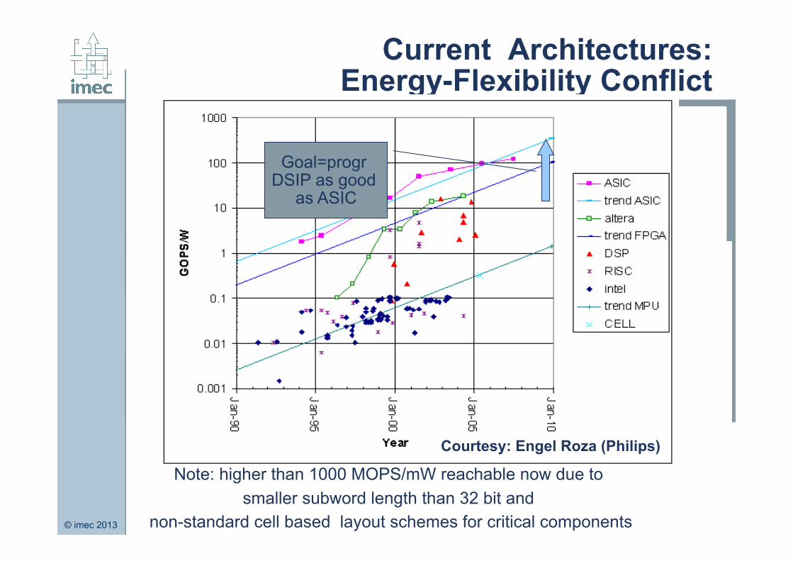
Current Architectures: Energy-Flexibility Conflict
Courtesy: Engel Roza (Philips)
Goal=progr DSIP as good
as ASIC
Note: higher than 1000 MOPS/mW reachable now due to smaller subword length than 32 bit and
non-standard cell based layout schemes for critical components
© imec 2013 IMEC confidential
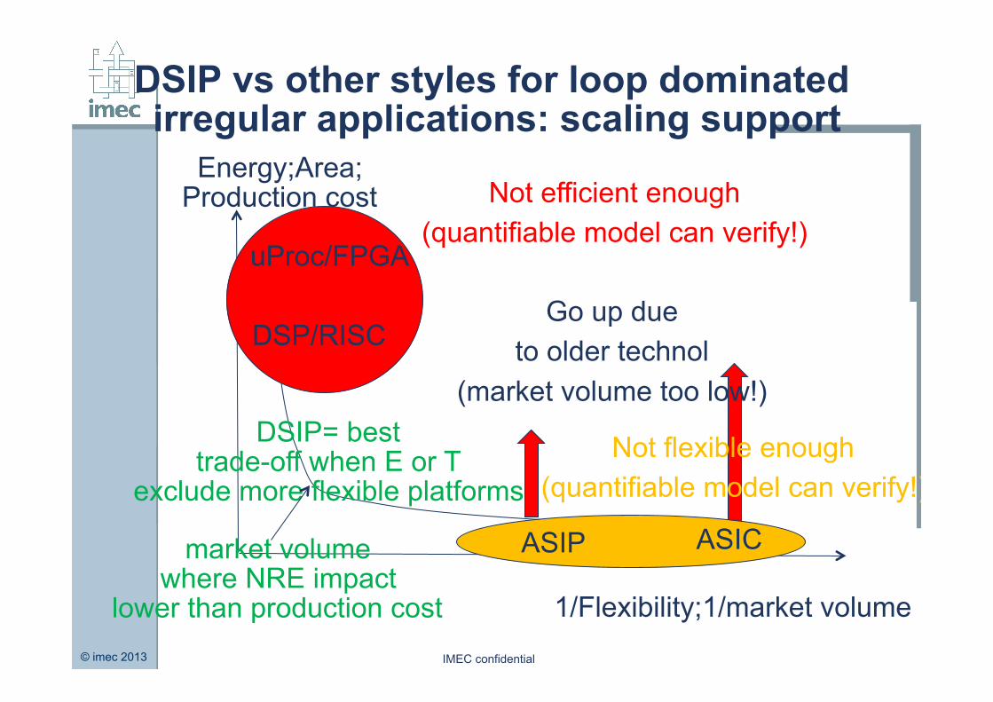
DSIP vs other styles for loop dominated irregular applications: scaling support
Energy;Area; Production cost
1/Flexibility;1/market volume
DSIP= best trade-off when E or T
exclude more flexible platforms
market volume where NRE impact
lower than production cost
Go up due to older technol
(market volume too low!)
ASIP ASIC
Not flexible enough (quantifiable model can verify!)
uProc/FPGA
DSP/RISC
Not efficient enough (quantifiable model can verify!)
© imec 2013 IMEC confidential
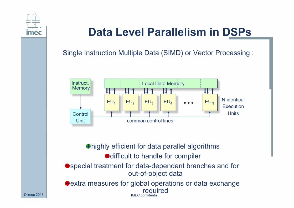
Data Level Parallelism in DSPs Single Instruction Multiple Data (SIMD) or Vector Processing :
! highly efficient for data parallel algorithms
! difficult to handle for compiler ! special treatment for data-dependant branches and for
out-of-object data ! extra measures for global operations or data exchange
required
Local Data Memory
common control lines Control
Unit
EU1 EU2 EU3 EU4 EUN N identical Execution
Units
Instruct. Memory
© imec 2013 IMEC confidential P.Raghavan and
F.Catthoor
11
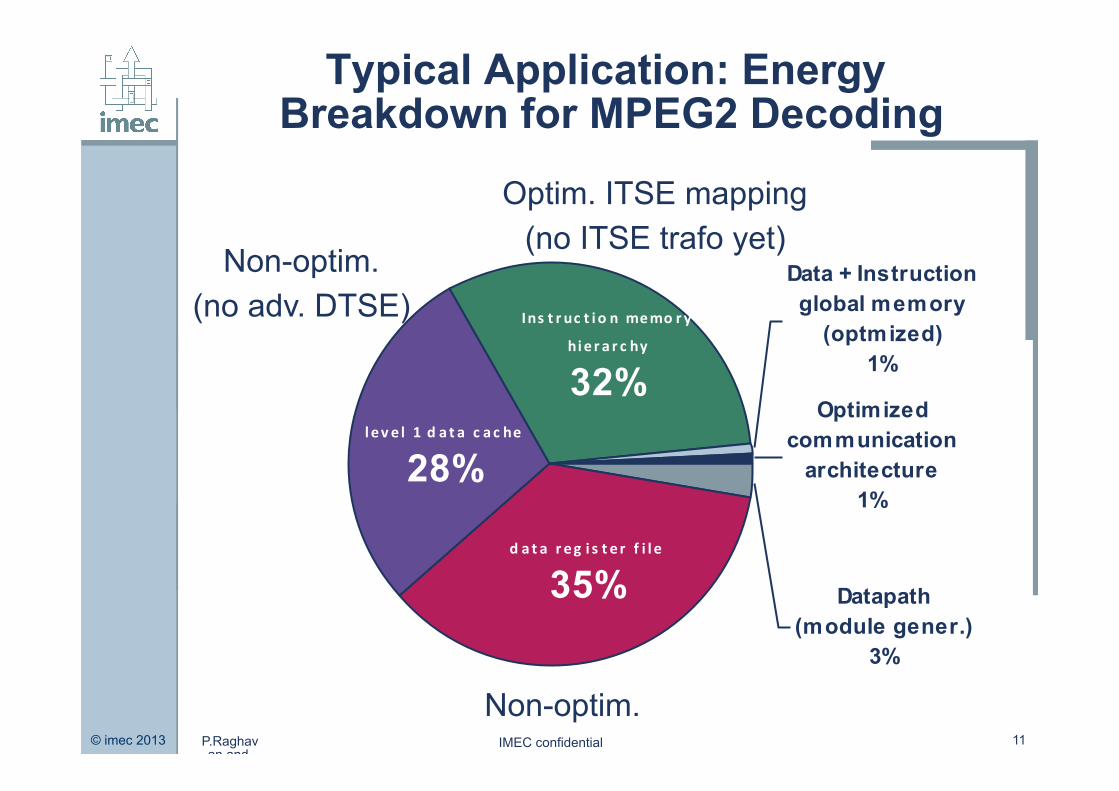
Typical Application: Energy Breakdown for MPEG2 Decoding
Data + Instruction global memory
(optmized)1%
Optimized communication
architecture1%
Ins t r uc t io n memo ry
hie r a r c hy
32%l ev e l 1 d a t a c ac he
28%
d at a r eg i s t e r f i l e
35% Datapath (module gener.)
3%
Non-optim.
Non-optim. (no adv. DTSE)
Optim. ITSE mapping (no ITSE trafo yet)
© imec 2013
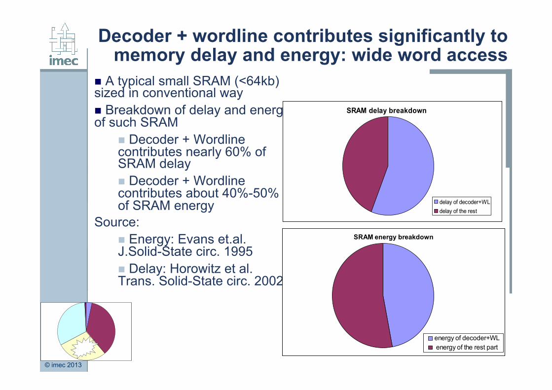
Decoder + wordline contributes significantly to memory delay and energy: wide word access
n A typical small SRAM (<64kb) sized in conventional way n Breakdown of delay and energy of such SRAM
n Decoder + Wordline contributes nearly 60% of SRAM delay n Decoder + Wordline contributes about 40%-50% of SRAM energy
Source: n Energy: Evans et.al. J.Solid-State circ. 1995 n Delay: Horowitz et al. Trans. Solid-State circ. 2002
SRAM delay breakdown
delay of decoder+WLdelay of the rest
SRAM energy breakdown
energy of decoder+WL energy of the rest part
© imec 2013
VWR VWR VW
R L
B
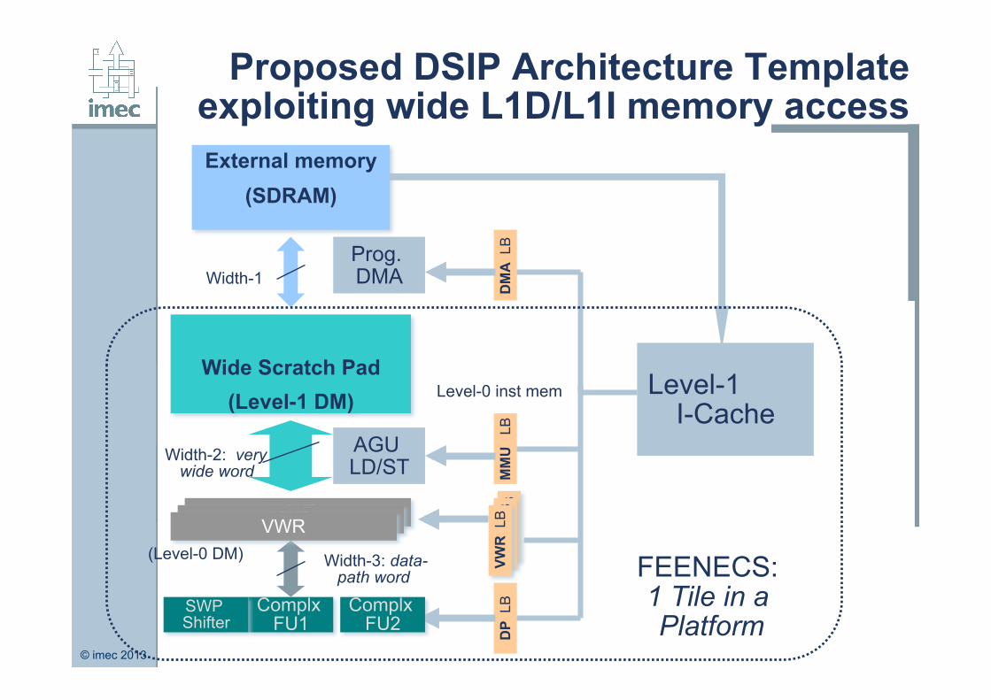
Proposed DSIP Architecture Template exploiting wide L1D/L1I memory access
Complx FU1
Wide Scratch Pad
(Level-1 DM)
External memory (SDRAM)
AGU LD/ST
Prog. DMA
VWR
LB
D
P L
B
MM
U
LB
DM
A L
B
Level-1 I-Cache
VWR
LB
VWR
SWP Shifter
Complx FU2
FEENECS: 1 Tile in a Platform
Level-0 inst mem
(Level-0 DM)
Width-1
Width-2: very wide word
Width-3: data-path word
© imec 2013 IMEC confidential
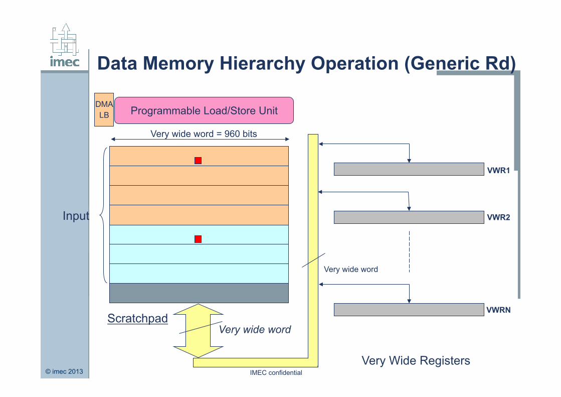
Data Memory Hierarchy Operation (Generic Rd)
Very wide word = 960 bits
Scratchpad
Programmable Load/Store Unit
Very wide word
Very wide word
Very Wide Registers
VWR1
VWR2
VWRN
Input
DMA LB
© imec 2013 IMEC confidential
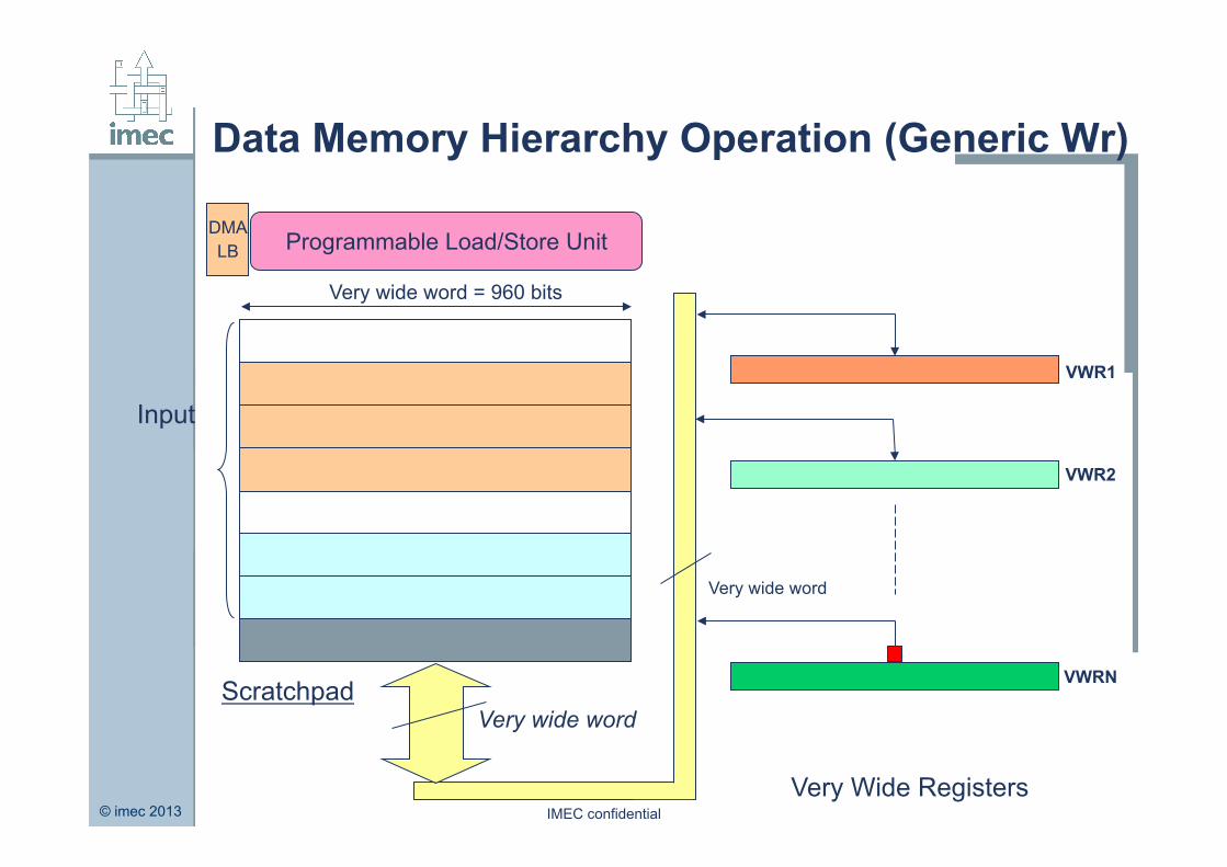
Data Memory Hierarchy Operation (Generic Wr)
Scratchpad
Very Wide Registers
VWR1
VWR2
VWRN
Input
Programmable Load/Store Unit DMA LB
Very wide word = 960 bits
Very wide word
Very wide word
© imec 2013 IMEC confidential
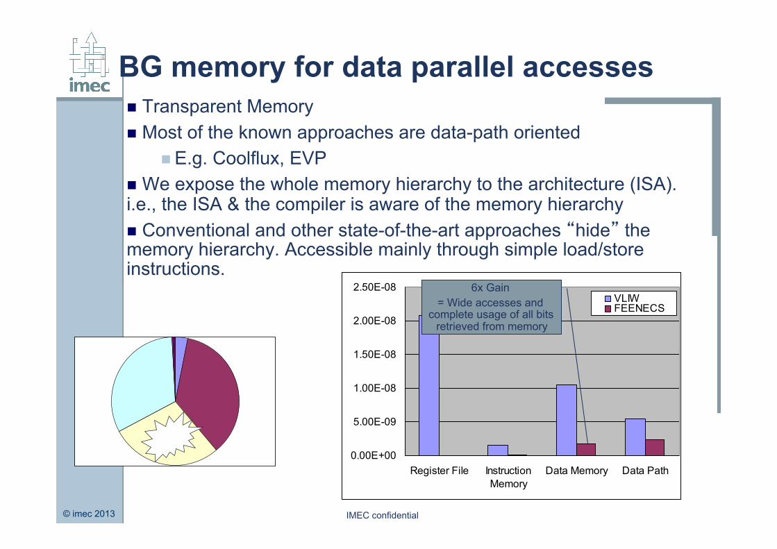
BG memory for data parallel accesses n Transparent Memory n Most of the known approaches are data-path oriented
n E.g. Coolflux, EVP n We expose the whole memory hierarchy to the architecture (ISA). i.e., the ISA & the compiler is aware of the memory hierarchy n Conventional and other state-of-the-art approaches “hide” the memory hierarchy. Accessible mainly through simple load/store instructions.
0.00E+00
5.00E-09
1.00E-08
1.50E-08
2.00E-08
2.50E-08
Register File InstructionMemory
Data Memory Data Path
VLIWFEENECS
6x Gain = Wide accesses and
complete usage of all bits retrieved from memory
© imec 2013 IMEC confidential
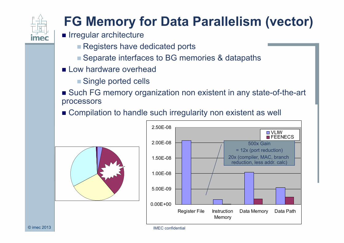
FG Memory for Data Parallelism (vector) n Irregular architecture
n Registers have dedicated ports n Separate interfaces to BG memories & datapaths
n Low hardware overhead n Single ported cells
n Such FG memory organization non existent in any state-of-the-art processors n Compilation to handle such irregularity non existent as well
0.00E+00
5.00E-09
1.00E-08
1.50E-08
2.00E-08
2.50E-08
Register File InstructionMemory
Data Memory Data Path
VLIWFEENECS
500x Gain = 12x (port reduction)
20x (compiler, MAC, branch reduction, less addr. calc)
© imec 2013 IMEC confidential
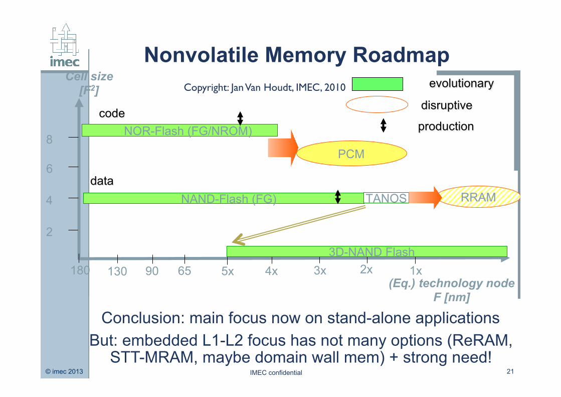
Nonvolatile Memory Roadmap
2
4
6
8
NAND-Flash (FG)
(Eq.) technology node F [nm]
Cell size [F2]
180 130 90 65 5x 3x
NOR-Flash (FG/NROM)
PCM
RRAM
2x
TANOS
4x 1x
code
data
evolutionary
disruptive
production
3D-NAND Flash
21
Copyright: Jan Van Houdt, IMEC, 2010
Conclusion: main focus now on stand-alone applications But: embedded L1-L2 focus has not many options (ReRAM,
STT-MRAM, maybe domain wall mem) + strong need!
© imec 2013 IMEC confidential
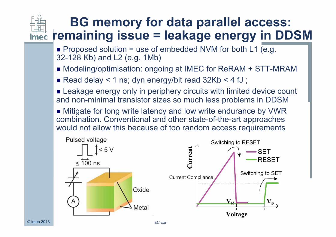
BG memory for data parallel access: remaining issue = leakage energy in DDSM n Proposed solution = use of embedded NVM for both L1 (e.g. 32-128 Kb) and L2 (e.g. 1Mb) n Modeling/optimisation: ongoing at IMEC for ReRAM + STT-MRAM n Read delay < 1 ns; dyn energy/bit read 32Kb < 4 fJ ; n Leakage energy only in periphery circuits with limited device count and non-minimal transistor sizes so much less problems in DDSM n Mitigate for long write latency and low write endurance by VWR combination. Conventional and other state-of-the-art approaches would not allow this because of too random access requirements
© imec 2013 IMEC confidential
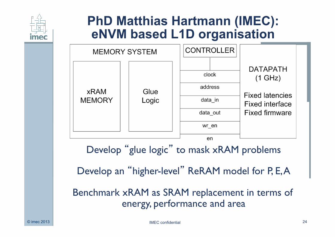
PhD Matthias Hartmann (IMEC): eNVM based L1D organisation
24
Develop “glue logic” to mask xRAM problems
Develop an “higher-level” ReRAM model for P, E, A
Benchmark xRAM as SRAM replacement in terms of energy, performance and area

© imec 2013 IMEC confidential
Write Frequency
25
0,00%
10,00%
20,00%
30,00%
40,00%
50,00%
© imec 2013 IMEC confidential
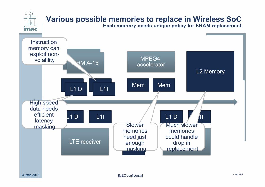
Various possible memories to replace in Wireless SoC Each memory needs unique policy for SRAM replacement
January 2013
ARM A-15 ARM A-15
L1 D L1 D
L1 D L1I
MPEG4 accelerator
Mem Mem
L2 Memory
LTE receiver
L1 D L1I
Turbo decoder HARQ Mem
L1 D L1I
Instruction memory can exploit non-
volatility
High speed data needs
efficient latency masking Slower
memories need just enough masking
Much slower memories
could handle drop in
replacement
© imec 2013 IMEC confidential
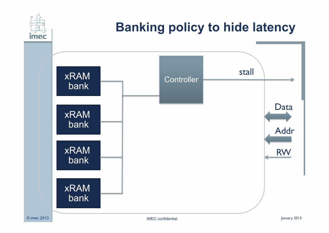
Banking policy to hide latency
January 2013
xRAM bank
xRAM bank
xRAM bank
xRAM bank
Controller
Data
Addr
RW
stall
© imec 2013 IMEC confidential
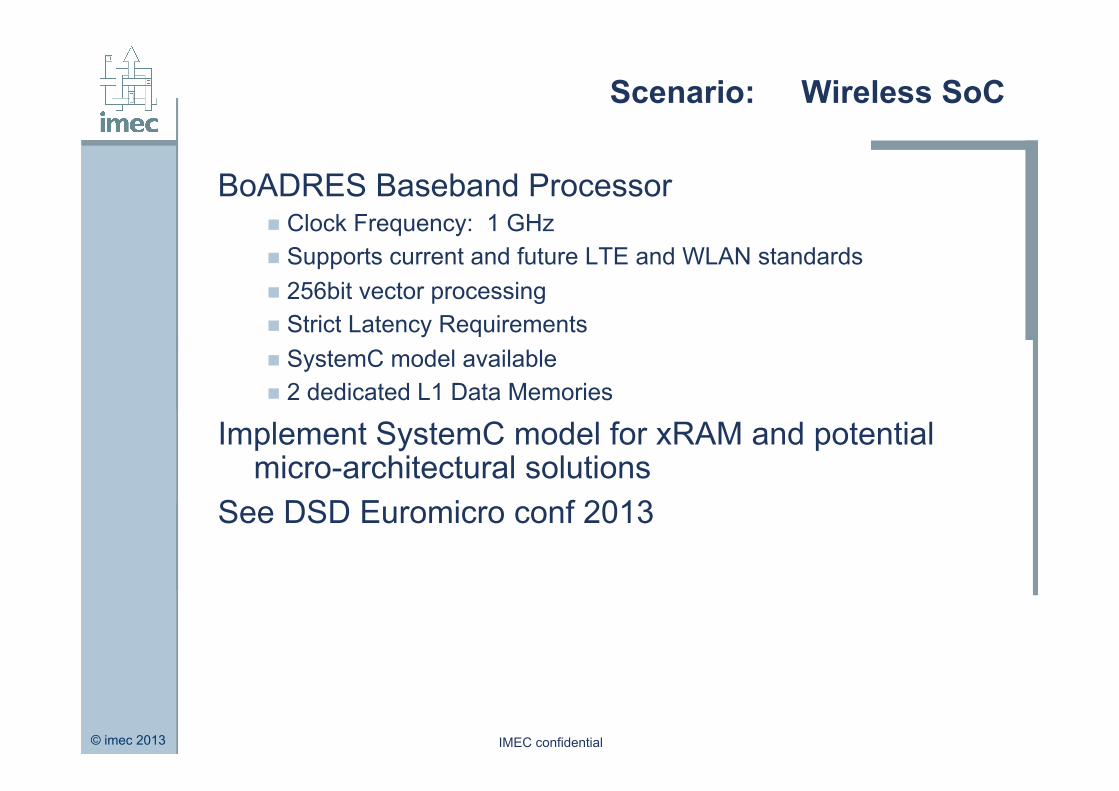
Scenario: Wireless SoC
BoADRES Baseband Processor n Clock Frequency: 1 GHz n Supports current and future LTE and WLAN standards n 256bit vector processing n Strict Latency Requirements n SystemC model available n 2 dedicated L1 Data Memories
Implement SystemC model for xRAM and potential micro-architectural solutions
See DSD Euromicro conf 2013
© imec 2013 IMEC confidential
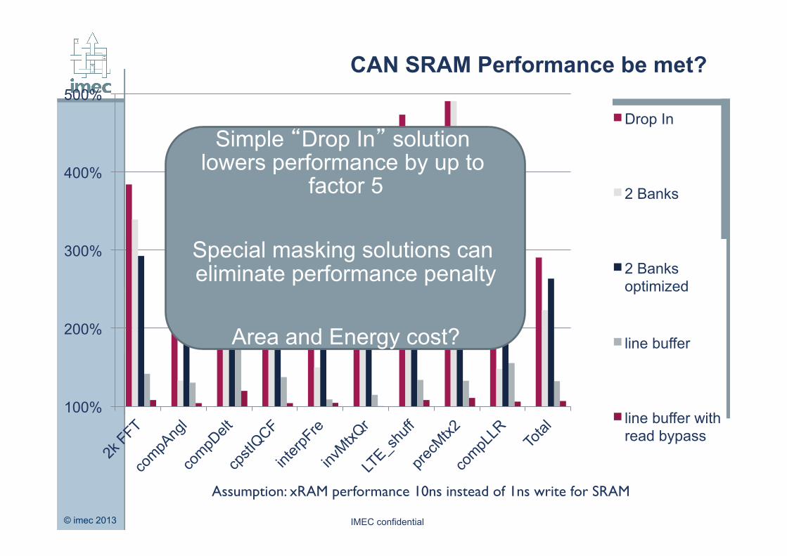
CAN SRAM Performance be met?
Assumption: xRAM performance 10ns instead of 1ns write for SRAM
100%
200%
300%
400%
500% Drop In
2 Banks
2 Banks optimized
line buffer
line buffer with read bypass
Simple “Drop In” solution lowers performance by up to
factor 5
Special masking solutions can eliminate performance penalty
Area and Energy cost?
© imec 2013 IMEC confidential
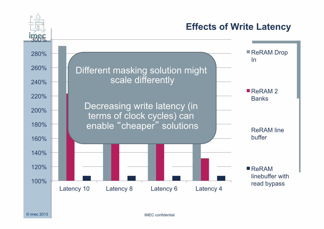
Effects of Write Latency
100%
120%
140%
160%
180%
200%
220%
240%
260%
280%
300%
Latency 10 Latency 8 Latency 6 Latency 4
ReRAM Drop In
ReRAM 2 Banks
ReRAM line buffer
ReRAM linebuffer with read bypass
Different masking solution might scale differently
Decreasing write latency (in terms of clock cycles) can enable “cheaper” solutions
© imec 2013
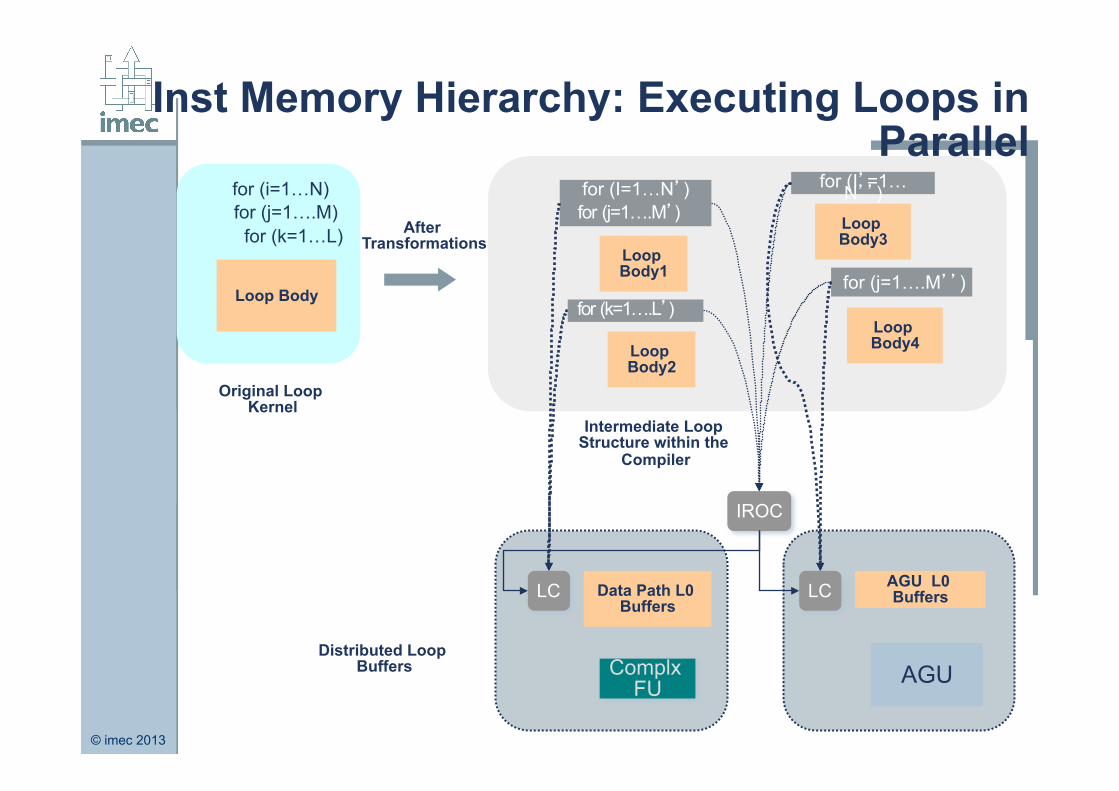
Inst Memory Hierarchy: Executing Loops in Parallel
for (i=1…N) for (j=1….M)
for (k=1…L)
for (I=1…N’) for (j=1….M’)
for (I’=1…N’’)
for (j=1….M’’)
AGU L0 Buffers LC
IROC
LC
Loop Body
Loop Body1
Loop Body3
Loop Body4
Data Path L0 Buffers
Loop Body2
for (k=1….L’)
Complx FU AGU
Original Loop Kernel
Intermediate Loop Structure within the
Compiler
Distributed Loop Buffers
After Transformations
© imec 2013 IMEC confidential
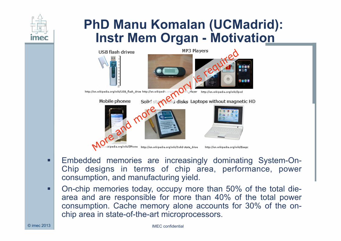
PhD Manu Komalan (UCMadrid): Instr Mem Organ - Motivation
§ Embedded memories are increasingly dominating System-On-Chip designs in terms of chip area, performance, power consumption, and manufacturing yield.
§ On-chip memories today, occupy more than 50% of the total die-area and are responsible for more than 40% of the total power consumption. Cache memory alone accounts for 30% of the on-chip area in state-of-the-art microprocessors.
© imec 2013 IMEC confidential
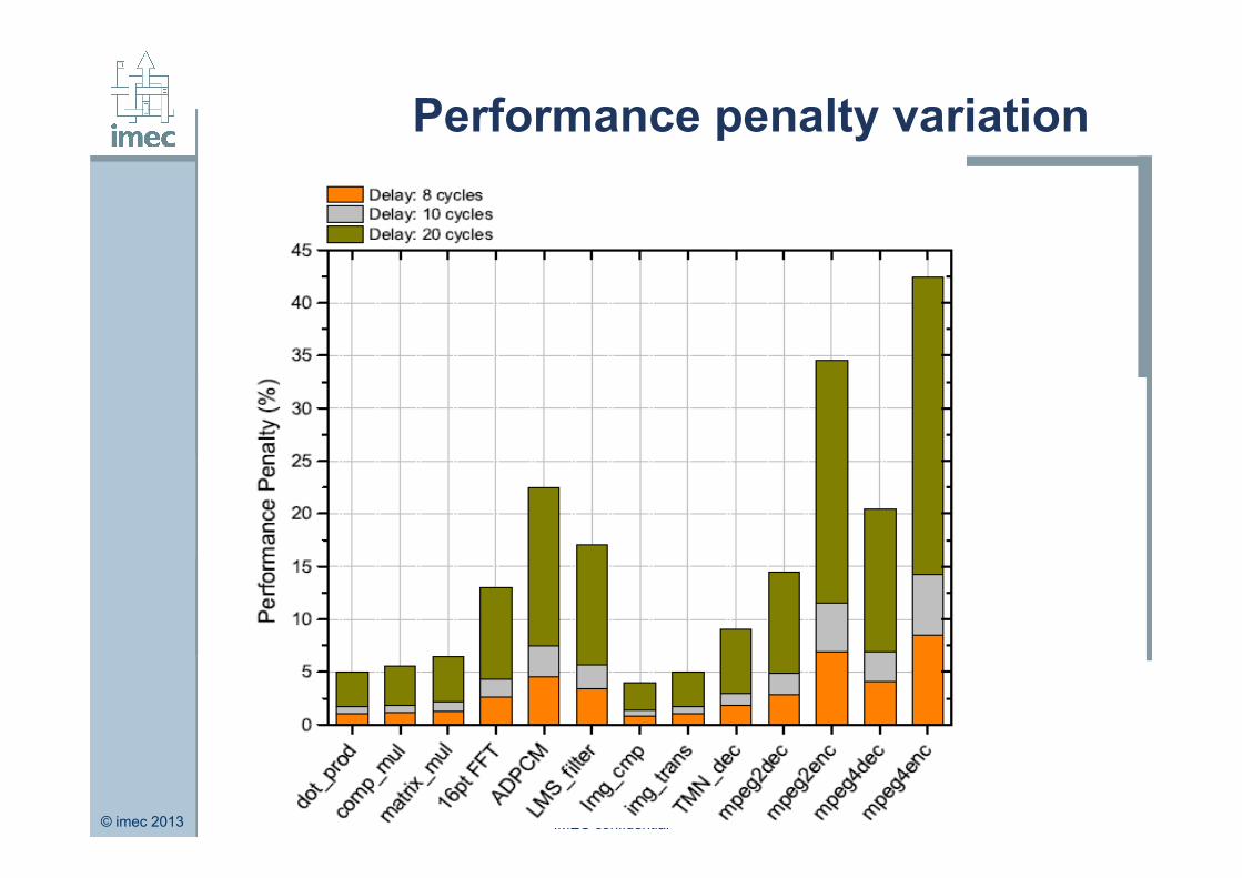
Sim 1
Performance penalty variation for different latencies (delays) in the original system with an NVM based I-cache.
No modification to cache organization. Conclusion: Simple substitution of SRAM by NVM is not
feasible. Architectural modifications are a must.
© imec 2013 IMEC confidential
Performance penalty variation
© imec 2013 IMEC confidential
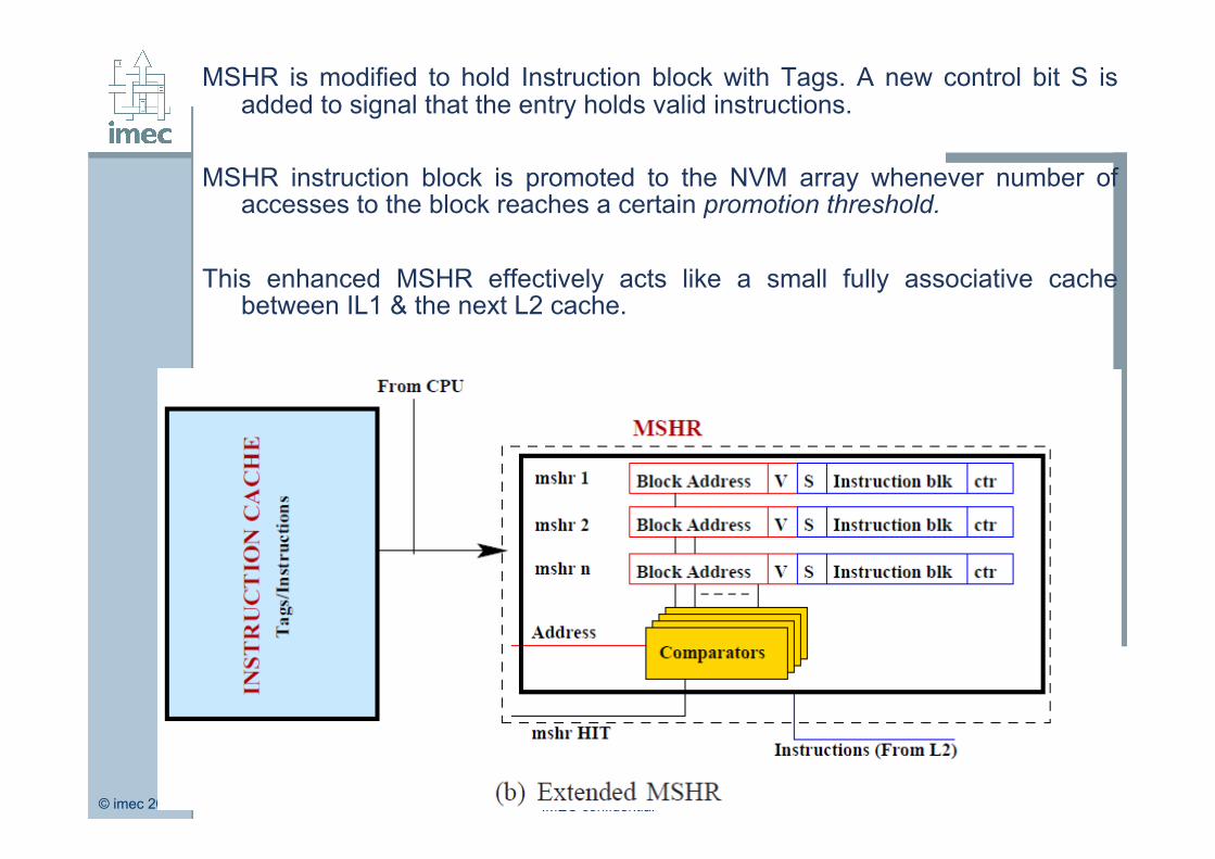
MSHR is modified to hold Instruction block with Tags. A new control bit S is added to signal that the entry holds valid instructions.
MSHR instruction block is promoted to the NVM array whenever number of
accesses to the block reaches a certain promotion threshold. This enhanced MSHR effectively acts like a small fully associative cache
between IL1 & the next L2 cache.
© imec 2013 IMEC confidential
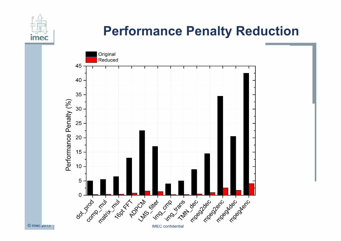
Performance Penalty Reduction
© imec 2013 IMEC confidential
Sim 6
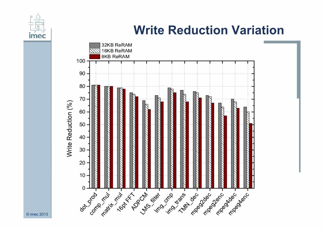
Endurance plays a huge part in the feasibility of these proposed caches.
Important aspect of the modification to the instruction cache
= reduction of writes to the I-cache. This has a significant bearing on endurance and lifetime.
We explore the influence of changing I-cache size on the
endurance. Endurance here can roughly be gauged by the write reduction (%).
© imec 2013 IMEC confidential
Write Reduction Variation
© imec 2013 IMEC confidential
Conclusions
Tuning of selective parameters can reduce the performance penalty due to the NVM to extremely tolerable levels ( ≈1%).
For ReRAM, we can obtain significant reductions in energy
consumption, given that the technology has a favourable read energy per access compared to SRAM.
Pareto-optimum values for the different parameters are application and
platform dependent. Architectural modifications proposed in this paper also offer endurance
gains, as a result of the filtering of some writes to the NVM array. Selective bancking can be explored to increase endurance further.

www.imec.be Worldwide collaboration with more than 500 companies and institutes.
IMEC – Kapeldreef 75 – B-3001 Leuven – Belgium – Tel. +32 16 281211 – Fax +32 16 229400 – www.imec.be