Embed Size (px)
Citation preview
1
Resistive switching behaviors of ReRAM
having W/CeO2/Si/TiN structure
C. Dou, K. Mukai, K. Kakushima, P. Ahmet, K. Tsutsui, A. Nishiyama,
N. Sugii, K. Natori, T. Hattori, and H. Iwai
1Frontier Research Center, Tokyo Institute of Technology 2Interdisciplinary Graduate School of Science and Engineering
219th ECS Meeting
Tokyo Institute of Technology
2
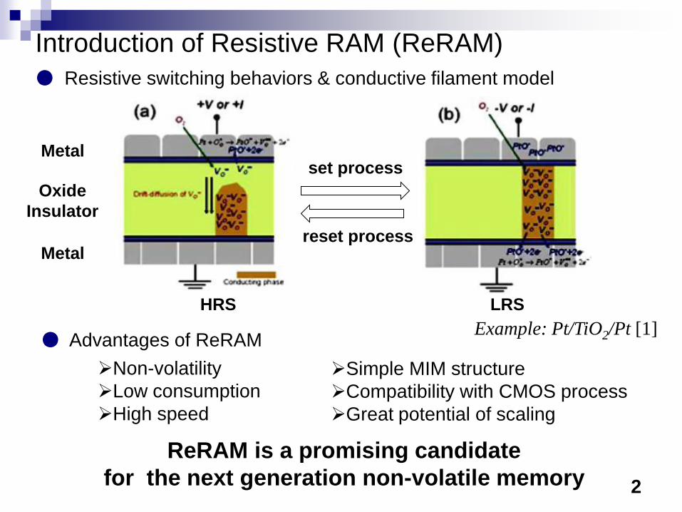
Introduction of Resistive RAM (ReRAM)
Non-volatility
Low consumption
High speed
Simple MIM structure
Compatibility with CMOS process
Great potential of scaling
Metal
Oxide
Insulator
Metal
set process
reset process
ReRAM is a promising candidate
for the next generation non-volatile memory
HRS LRS
● Resistive switching behaviors & conductive filament model
● Advantages of ReRAMExample: Pt/TiO2/Pt [1]
3
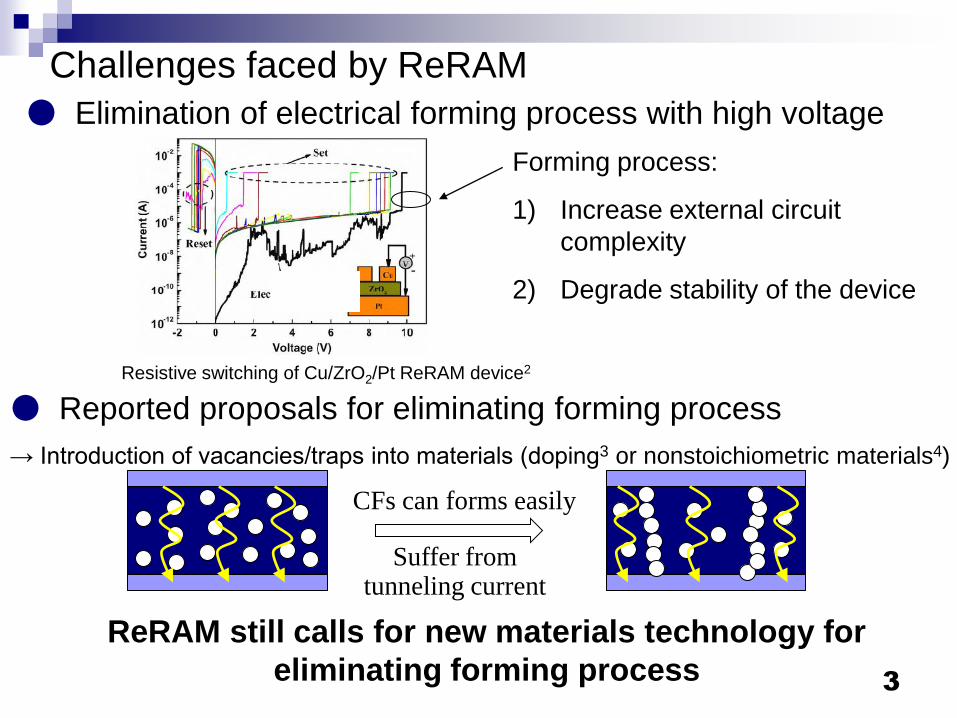
Challenges faced by ReRAM
Resistive switching of Cu/ZrO2/Pt ReRAM device2
ReRAM still calls for new materials technology for
eliminating forming process
Forming process:
1) Increase external circuit
complexity
2) Degrade stability of the device
● Elimination of electrical forming process with high voltage
● Reported proposals for eliminating forming process
→ Introduction of vacancies/traps into materials (doping3 or nonstoichiometric materials4)
CFs can forms easily
Suffer from tunneling current
4
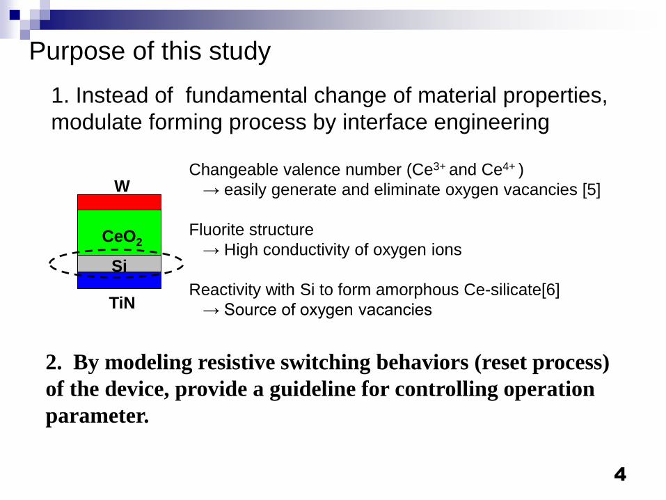
Purpose of this study
CeO2
Si
W
TiN
1. Instead of fundamental change of material properties,
modulate forming process by interface engineering
2. By modeling resistive switching behaviors (reset process)
of the device, provide a guideline for controlling operation
parameter.
Changeable valence number (Ce3+ and Ce4+ )
→ easily generate and eliminate oxygen vacancies [5]
Fluorite structure
→ High conductivity of oxygen ions
Reactivity with Si to form amorphous Ce-silicate[6]
→ Source of oxygen vacancies
5
Part I: Modulation of forming process of CeO2
ReRAM by incoporating Si buffer layer
1. Device structure and fabrication
2. Resistive switching properties
3. The effect of Si buffer layer
4. Proposed model for Si buffer layer

6
Al
n+-Si wafer
TiN
Si
CeO2
W
Cell size
20 mm *20mm
20 nm
15 nm
50 nm
200 nm
SiO2
0/1 nm
Growth of SiO2 insulator
(thermal oxidation)
Patterning contact window
Cleaning (SPM + DHF)
Deposition of TiN bottom electrode
(RF sputter)
n+-Si wafer (0.02 < W cm)
Deposition of W top electrode
(RF sputter)
Deposition of Si buffer layer
(RF sputter)
Deposition of CeO2 switching layer
(electron beam)
Electrode patterning process
Evaporation of Al back contact
A
V
Materials and structure are
suitable for practical application Annealing 400oC, 30s, N2
Device structure and fabrication

7
1.0E-10
1.0E-09
1.0E-08
1.0E-07
1.0E-06
1.0E-05
1.0E-04
1.0E-03
1.0E-02
-3 -2 -1 0 1 2 3
1st cycle
2nd cycle
10th cycle
Bias ( V )
Cu
rren
t(A
)
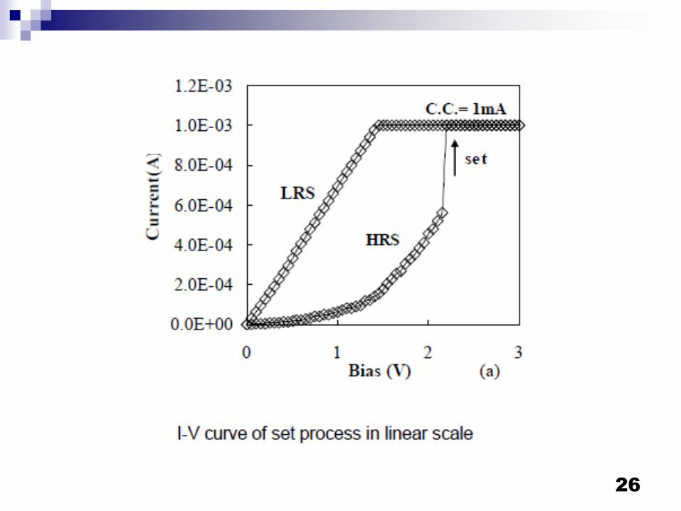
Forming processHRS
LRS
Typical resistive switching behavior of the device
I-V characteristics of W/CeO2/Si/TiN under sweeping voltage
W/CeO2/Si/TiN shows bipolar resistive switching
behaviors without requiring a high forming voltage
Set Reset
VF (Forming voltage)VsetVstop
Compliance Current (C.C.)
①
②
③④
⑤
8
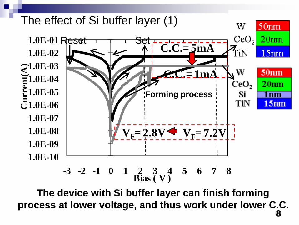
The effect of Si buffer layer (1)
1.0E-10
1.0E-09
1.0E-08
1.0E-07
1.0E-06
1.0E-05
1.0E-04
1.0E-03
1.0E-02
1.0E-01
-3 -2 -1 0 1 2 3 4 5 6 7 8Bias ( V )
Cu
rren
t(A
)
C.C.= 5mA
C.C.= 1mA
VF= 2.8V VF= 7.2V
The device with Si buffer layer can finish forming
process at lower voltage, and thus work under lower C.C.
Reset Set
Forming process
9
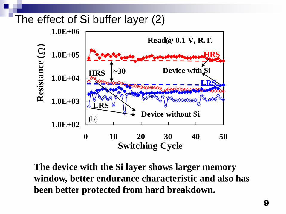
The effect of Si buffer layer (2)
1.0E+02
1.0E+03
1.0E+04
1.0E+05
1.0E+06
0 10 20 30 40 50
Switching Cycle
Res
ista
nce
(W
)
HRS
LRS
Read@ 0.1 V, R.T.
Device without Si
Device with Si
(b)
HRS
LRS
~30
International 9/17
The device with the Si layer shows larger memory
window, better endurance characteristic and also has
been better protected from hard breakdown.
10
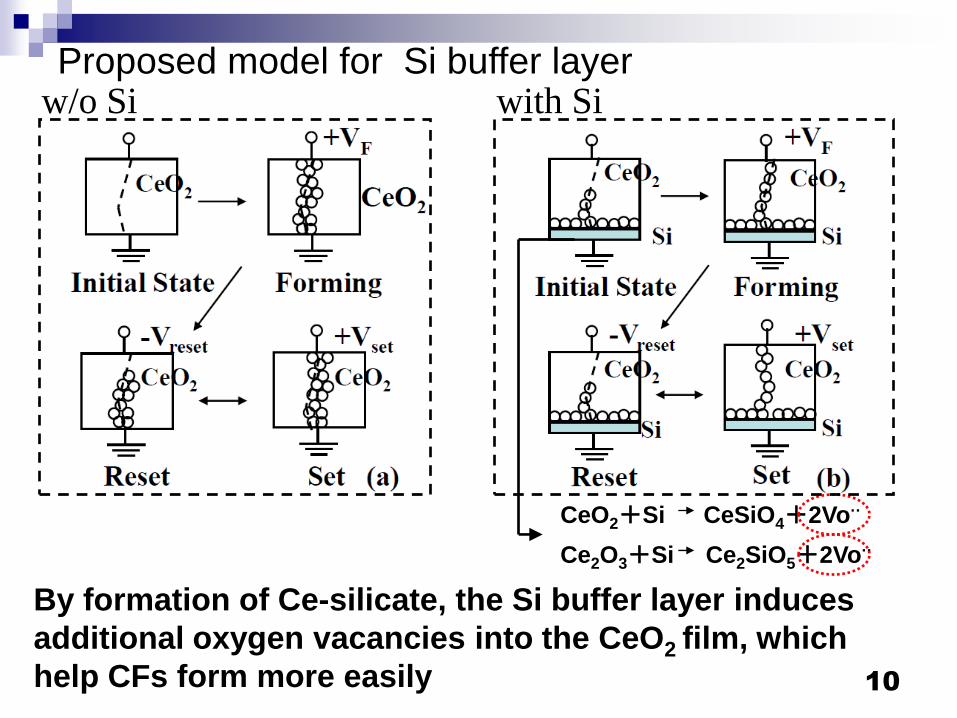
CeO2+Si CeSiO4+2Vo··
Ce2O3+Si Ce2SiO5+2Vo··
By formation of Ce-silicate, the Si buffer layer induces
additional oxygen vacancies into the CeO2 film, which
help CFs form more easily
Proposed model for Si buffer layerw/o Si with Si
11
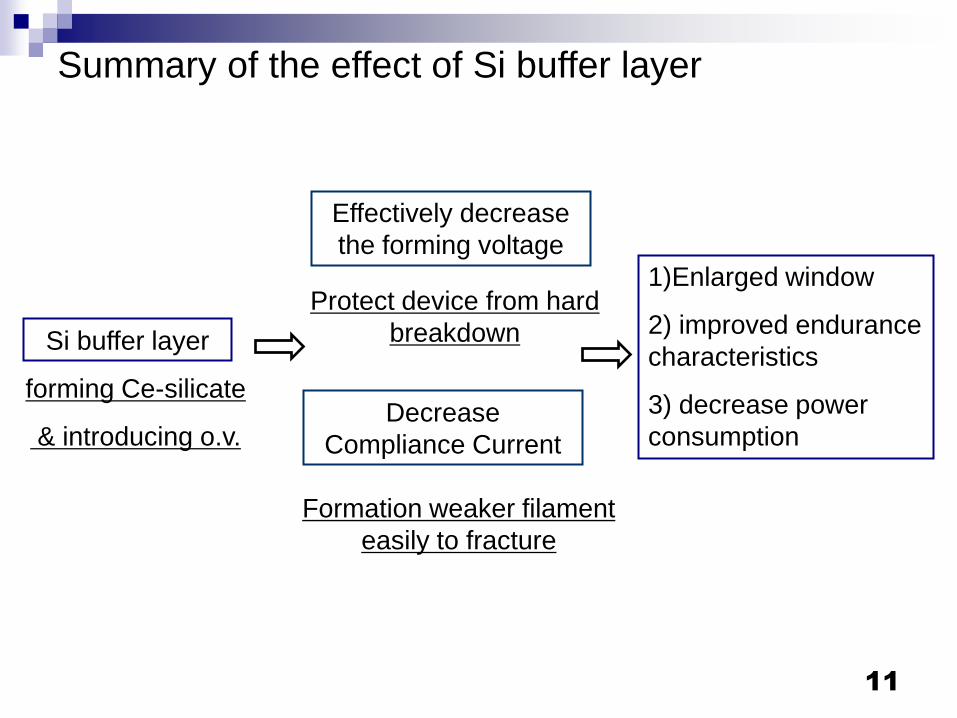
Si buffer layer
Effectively decrease
the forming voltage
Decrease
Compliance Current
Protect device from hard
breakdown
Formation weaker filament
easily to fracture
1)Enlarged window
2) improved endurance
characteristics
3) decrease power
consumption
Summary of the effect of Si buffer layer
forming Ce-silicate
& introducing o.v.
12
Part II: Modeling resistive switching behaviors of
the device (reset process)
1. Influence of Vstop on resistive switching of the device
2. Modeling the reset process
13
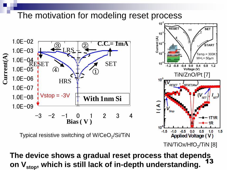
1.0E-09
1.0E-08
1.0E-07
1.0E-06
1.0E-05
1.0E-04
1.0E-03
1.0E-02
-3 -2 -1 0 1 2 3 4Bias ( V )
Cu
rren
t(A
)
④ ①
②③
With 1nm Si
HRS
LRS
SETRESET
C.C.= 1mA
Typical resistive switching of W/CeO2/Si/TiN
The motivation for modeling reset process
The device shows a gradual reset process that depends
on Vstop, which is still lack of in-depth understanding.
Vstop = -3V
TiN/TiOx/HfO2/TiN [8]
TiN/ZnO/Pt [7]
14
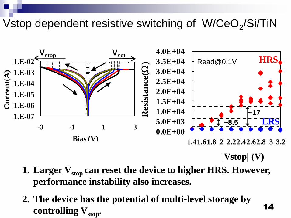
Vstop dependent resistive switching of W/CeO2/Si/TiN
0.0E+00
5.0E+03
1.0E+04
1.5E+04
2.0E+04
2.5E+04
3.0E+04
3.5E+04
4.0E+04
1.41.61.8 2 2.22.42.62.8 3 3.2
|Vstop| (V)
Resi
stan
ce(W
) HRS
LRS
~8.5
~171.E-07
1.E-06
1.E-05
1.E-04
1.E-03
1.E-02
-3 -1 1 3
Bias (V)
Cu
rren
t(A
)
1. Larger Vstop can reset the device to higher HRS. However,
performance instability also increases.
2. The device has the potential of multi-level storage by
controlling Vstop.
Vstop Vset
15
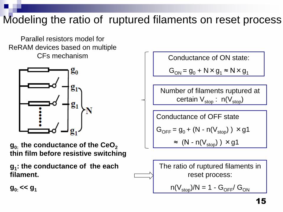
Modeling the ratio of ruptured filaments on reset process
Conductance of ON state:
GON = g0 + N×g1 ≈ N×g1
Number of filaments ruptured at
certain Vstop : n(Vstop)
Parallel resistors model for
ReRAM devices based on multiple
CFs mechanism
Conductance of OFF state
GOFF = g0 + (N - n(Vstop) ) ×g1
≈ (N - n(Vstop) ) ×g1
The ratio of ruptured filaments in
reset process:
n(Vstop)/N = 1 - GOFF/ GON
g0: the conductance of the CeO2
thin film before resistive switching
g1: the conductance of the each
filament.
g0: << g1
16
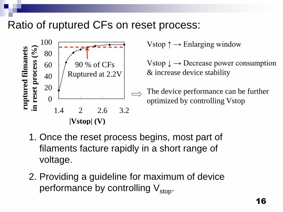
1. Once the reset process begins, most part of
filaments facture rapidly in a short range of
voltage.
2. Providing a guideline for maximum of device
performance by controlling Vstop.
Ratio of ruptured CFs on reset process:
Vstop ↑ → Enlarging window
Vstop ↓ → Decrease power consumption
& increase device stability
The device performance can be further
optimized by controlling Vstop0
20
40
60
80
100
1.4 2 2.6 3.2rup
ture
d f
ilm
an
ets
in r
eset
pro
cess
(%
)
|Vstop| (V)
90 % of CFs
Ruptured at 2.2V
17
Summary
1. Successful improvement of performance CeO2 ReRAM
by incorporating a Si buffer layer at bottom interface.
(forming voltage, window, endurance and power
consumption)
2. The effect of the Si buffer layer is attributed to the
formation of silicate, which serves as a source of oxygen
vacancies.
3. Vstop dependent reset process of the device is
investigated, and a guideline for Vstop control is provided.
Reference
1. R. Waser and M. Aonom, Nature Materials. 6, 833 (2007)
2. Q. liu, et, al. , 2009. ESSDERC
3. Q. Liu, W.Guan, S.Long, R.Jia, and M.Liu, Appl. Phys. Lett. 92, 012117 (2008)
4. X. Sun, B. Sun, L. Liu, N. Xu, X. Liu, R. Han, J. Kang, G. Xiong and T, P. Ma,
IEEE Electron Device Lett. 30, 4 (2009)
5. F. Esch, et. al, Science, 309, 752-755 (2005)
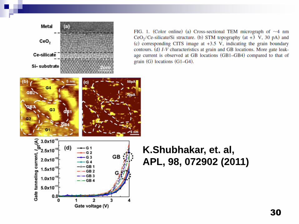
6. K.Shubhakar, et. al, APL, 98, 072902 (2011)
7. N. Xun, et. al, APPLIED PHYSICS LETTERS 92, 232112 2008
8. L. Goux, et. al, APPLIED PHYSICS LETTERS 97, 243509 2010
18

19
Thank you very much!Welcome for comments and questions

20
Back up materials
21
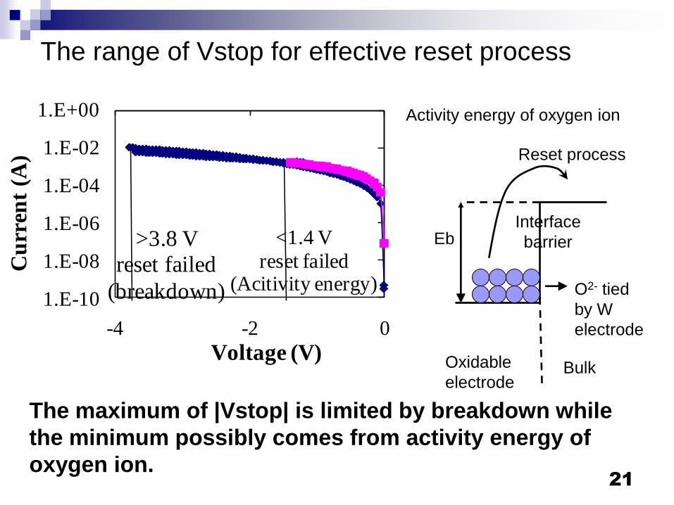
The range of Vstop for effective reset process
Eb
O2- tied
by W
electrode
Interface
barrier
Reset process
Activity energy of oxygen ion
The maximum of |Vstop| is limited by breakdown while
the minimum possibly comes from activity energy of
oxygen ion.
1.E-10
1.E-08
1.E-06
1.E-04
1.E-02
1.E+00
-4 -2 0
Voltage (V)
Cu
rren
t (A
)
>3.8 V
reset failed
(breakdown)
<1.4 V
reset failed (Acitivity energy)
Oxidable
electrodeBulk
22
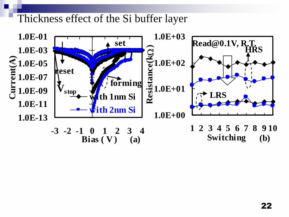
Thickness effect of the Si buffer layer
1.0E-13
1.0E-11
1.0E-09
1.0E-07
1.0E-05
1.0E-03
1.0E-01
-3 -2 -1 0 1 2 3 4
with 1nm Si
with 2nm Si
Bias ( V )
Cu
rren
t(A
)
reset
set
forming
(a)
Vstop
1.0E+00
1.0E+01
1.0E+02
1.0E+03
1 2 3 4 5 6 7 8 9 10Switching
Resi
sta
nce(k
W)
[email protected], R.T.
LRS
(b)

23
2CeO2
Ce2O3 + ½ O2 +Vo··
Oxygen ions at
grain boundary
W electrode
TiN electrode
CeO2
Initial state
on state (LRS) off state (HRS)
Forming process
+VFormation of oxygen
vacancies:
-2e-
E
+V -V elimination of oxygen
vacancies
Ce2O3 + ½ O2 +Vo··
2CeO2+2e-
24
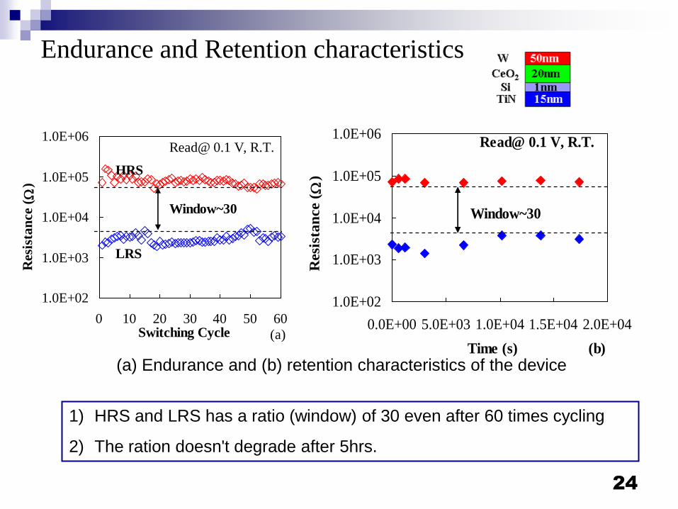
(a) Endurance and (b) retention characteristics of the device
Endurance and Retention characteristics
1.0E+02
1.0E+03
1.0E+04
1.0E+05
1.0E+06
0 10 20 30 40 50 60Switching Cycle
Resi
stan
ce (
W)
Window~30
HRS
LRS
Read@ 0.1 V, R.T.
(a)
1.0E+02
1.0E+03
1.0E+04
1.0E+05
1.0E+06
0.0E+00 5.0E+03 1.0E+04 1.5E+04 2.0E+04
Time (s)
Resi
sta
nce (
W)
Read@ 0.1 V, R.T.
Window~30
(b)
1) HRS and LRS has a ratio (window) of 30 even after 60 times cycling
2) The ration doesn't degrade after 5hrs.
25
0.E+00
1.E+04
2.E+04
3.E+04
4.E+04
5.E+04
6.E+04
7.E+04
8.E+04
9.E+04
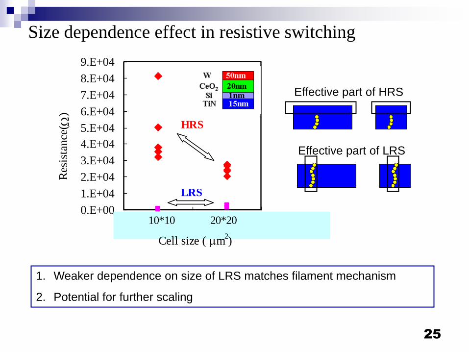
5 10 15 20 25 10*10 20*20
HRS
LRS
Res
ista
nce
( W)
Cell size ( mm2)
Size dependence effect in resistive switching
1. Weaker dependence on size of LRS matches filament mechanism
2. Potential for further scaling
Effective part of HRS
Effective part of LRS
26
27
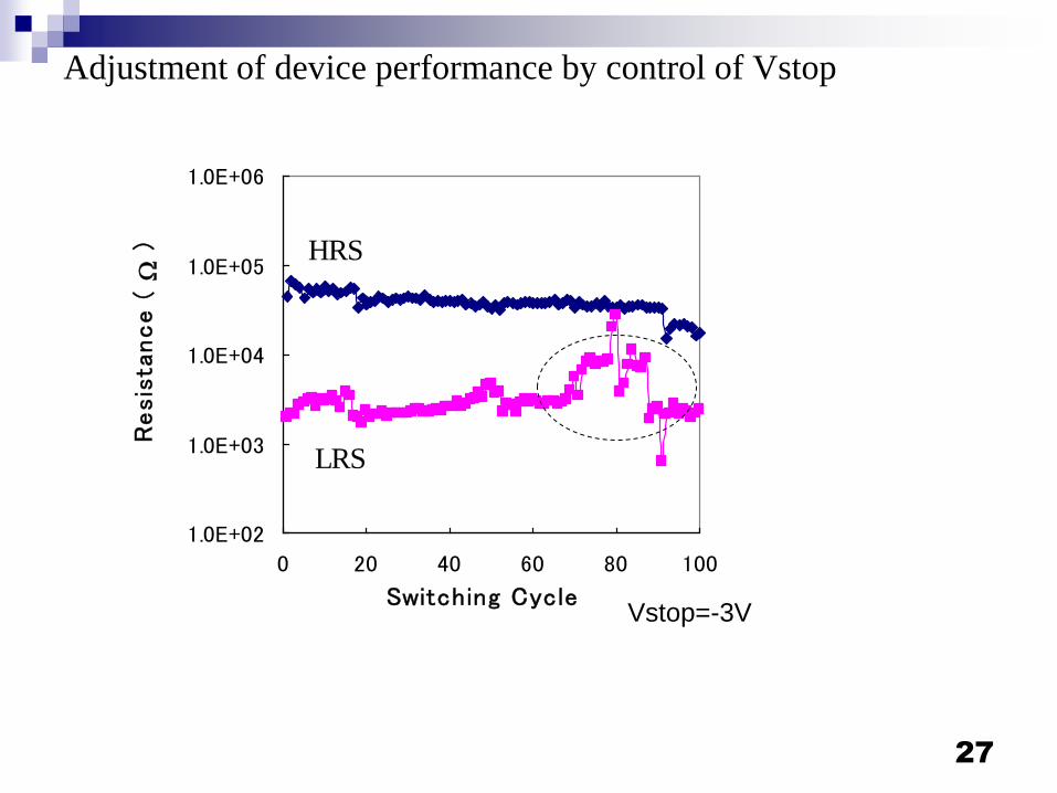
Adjustment of device performance by control of Vstop
1.0E+02
1.0E+03
1.0E+04
1.0E+05
1.0E+06
0 20 40 60 80 100
Switching Cycle
Resis
tance (
W )
LRS
HRS
Vstop=-3V
28
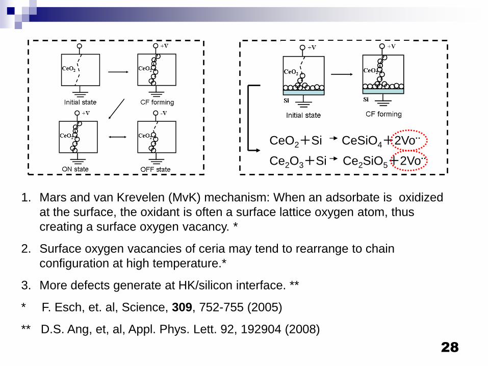
1. Mars and van Krevelen (MvK) mechanism: When an adsorbate is oxidized
at the surface, the oxidant is often a surface lattice oxygen atom, thus
creating a surface oxygen vacancy. *
2. Surface oxygen vacancies of ceria may tend to rearrange to chain
configuration at high temperature.*
3. More defects generate at HK/silicon interface. **
* F. Esch, et. al, Science, 309, 752-755 (2005)
** D.S. Ang, et, al, Appl. Phys. Lett. 92, 192904 (2008)
CeO2+Si CeSiO4+2Vo··
Ce2O3+Si Ce2SiO5+2Vo··
29
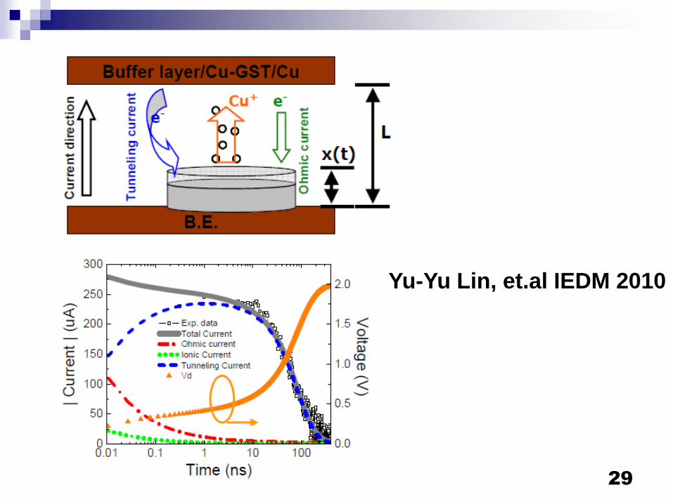
Yu-Yu Lin, et.al IEDM 2010
30
K.Shubhakar, et. al,
APL, 98, 072902 (2011)


![Resistive RAM embedded MCU - Panasonic · Industry’s first sampling MCU with built-in Resistive RAM (ReRAM) Abstract Added value Application Smart meter ... EWme-ReRAM1.ppt [Kompatibilitätsmodus]](https://img.pdfslide.us/doc/110x75/5b37177e7f8b9a5f288da56f/resistive-ram-embedded-mcu-panasonic-industrys-first-sampling-mcu-with.jpg)

![Resistive RAM embedded MCU - Panasonic s first sampling MCU with built-in Resistive RAM (ReRAM) Abstract Added value Application Smart meter ... EWme-ReRAM1.ppt [Kompatibilitätsmodus]](https://img.pdfslide.us/doc/110x75/5aaa87387f8b9a9a188e5792/resistive-ram-embedded-mcu-panasonic-s-first-sampling-mcu-with-built-in-resistive.jpg)