Embed Size (px)
Citation preview
Memory Technologies
Muhammad Touqir Pasha
ISY
Outline
• Overview of memory systems
• History
• Memory Types
• Current Trends
• Emerging technologies
• Memristors
• Conclusion

History
• “Micrologic family Until the reductions are possible in other portions of a computer – especially the memory system – progress will be slower. There’s not too much point for a “pea-sized” logic element and a “barrel-sized” memory system, is the way the founders put it.” 1
1-Solid State Journal September/October 1960
History
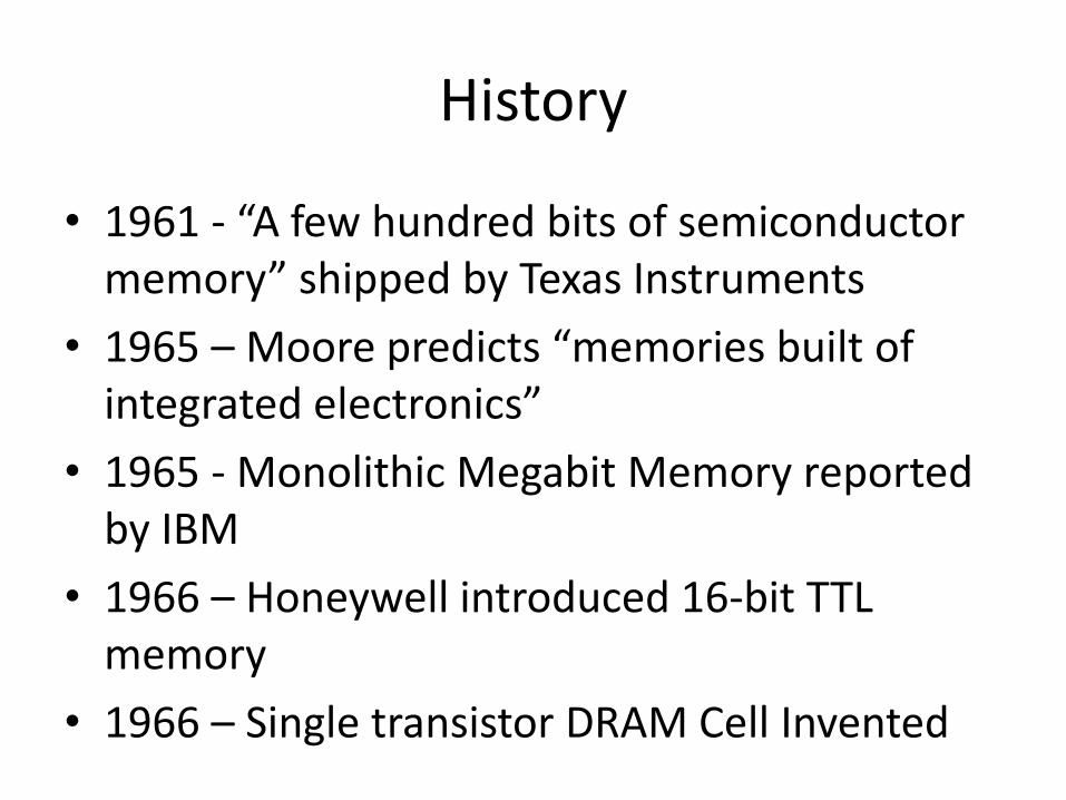
• 1961 - “A few hundred bits of semiconductor memory” shipped by Texas Instruments
• 1965 – Moore predicts “memories built of integrated electronics”
• 1965 - Monolithic Megabit Memory reported by IBM
• 1966 – Honeywell introduced 16-bit TTL memory
• 1966 – Single transistor DRAM Cell Invented
Types of Memories
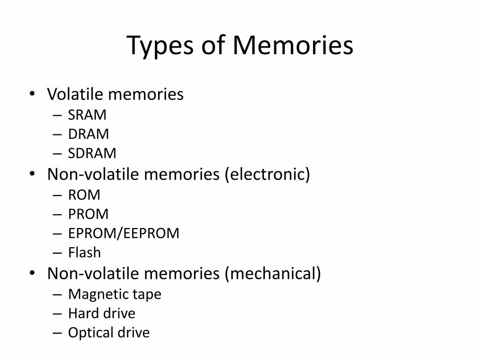
• Volatile memories – SRAM – DRAM – SDRAM
• Non-volatile memories (electronic) – ROM – PROM – EPROM/EEPROM – Flash
• Non-volatile memories (mechanical) – Magnetic tape – Hard drive – Optical drive
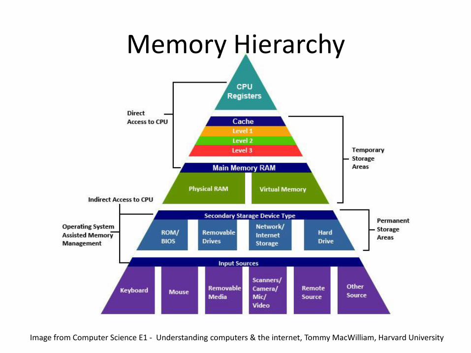
Memory Hierarchy
Image from Computer Science E1 - Understanding computers & the internet, Tommy MacWilliam, Harvard University
Requirements on Memories
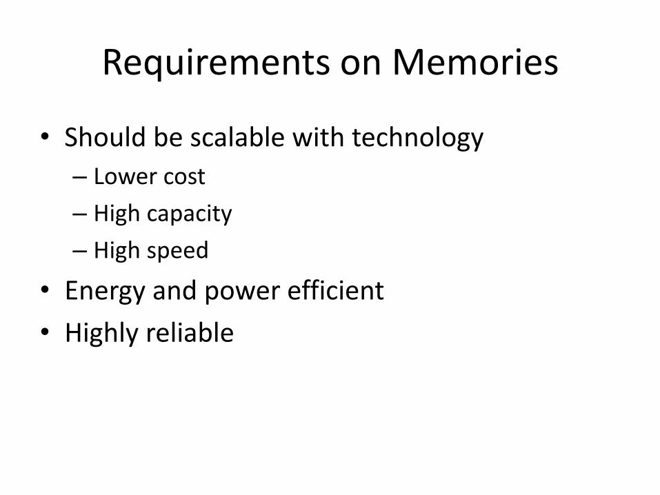
• Should be scalable with technology
– Lower cost
– High capacity
– High speed
• Energy and power efficient
• Highly reliable
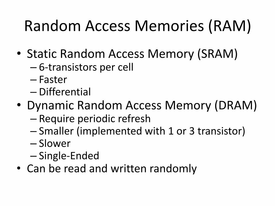
Random Access Memories (RAM)
• Static Random Access Memory (SRAM) – 6-transistors per cell – Faster – Differential
• Dynamic Random Access Memory (DRAM) – Require periodic refresh – Smaller (implemented with 1 or 3 transistor) – Slower – Single-Ended
• Can be read and written randomly
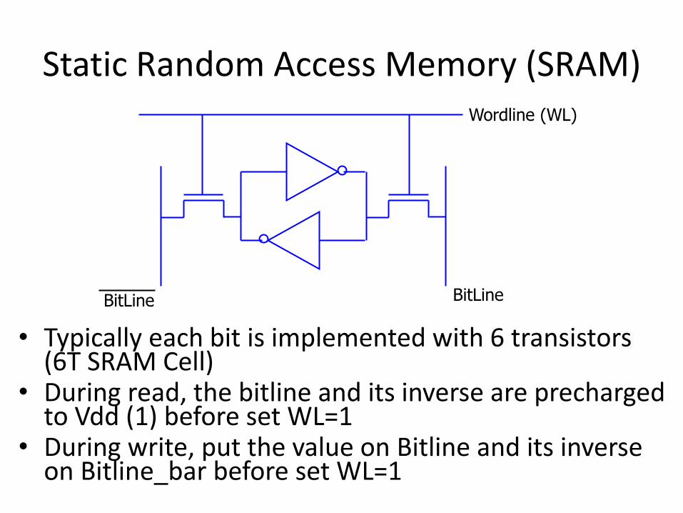
Static Random Access Memory (SRAM)
• Typically each bit is implemented with 6 transistors (6T SRAM Cell)
• During read, the bitline and its inverse are precharged to Vdd (1) before set WL=1
• During write, put the value on Bitline and its inverse on Bitline_bar before set WL=1
BitLine BitLine
Wordline (WL)
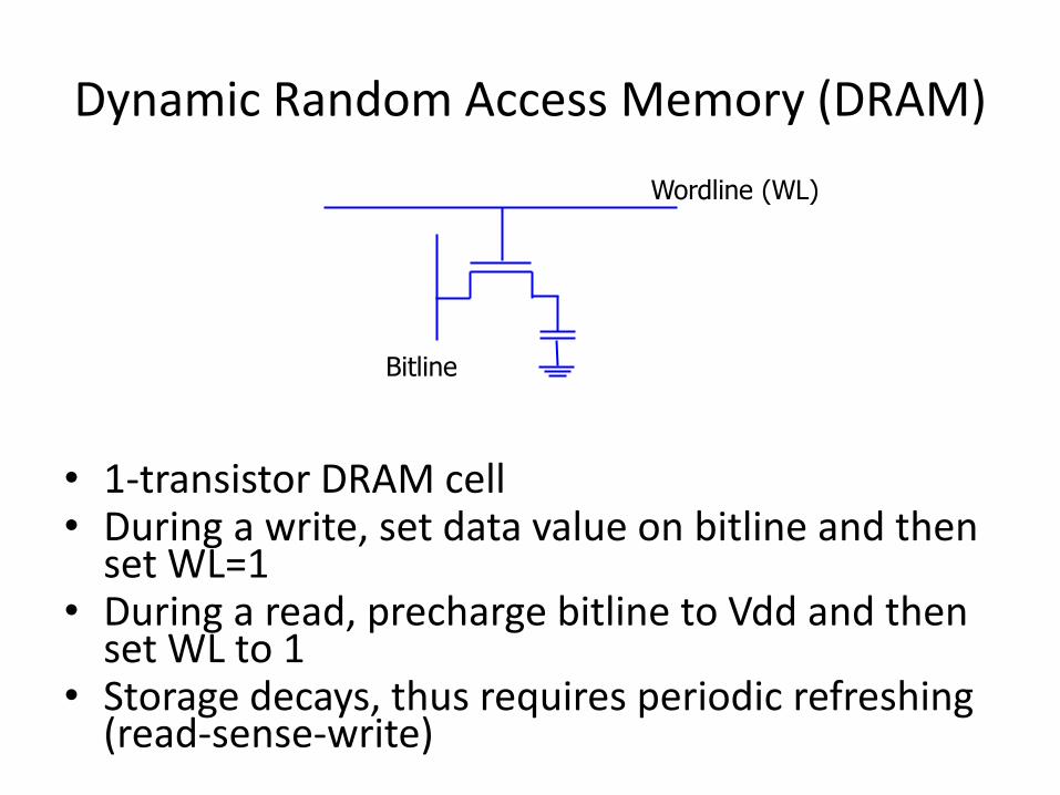
Dynamic Random Access Memory (DRAM)
• 1-transistor DRAM cell • During a write, set data value on bitline and then
set WL=1 • During a read, precharge bitline to Vdd and then
set WL to 1 • Storage decays, thus requires periodic refreshing
(read-sense-write)
Bitline
Wordline (WL)
Scaling Issues in DRAM
• DRAM is charged based memory
– Large capacitor required for reliable sensing
– Access transistor should be large enough for low leakage and high retention time.
– Scaling beyond 40-35nm (2013) is challenging [ITRS, 2009].
• DRAM capacity, cost, and energy/power hard to scale.
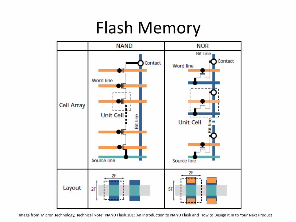
Flash Memory
Image from Micron Technology, Technical Note: NAND Flash 101: An Introduction to NAND Flash and How to Design It In to Your Next Product
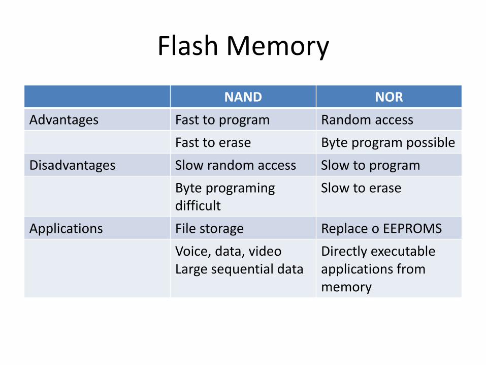
Flash Memory
NAND NOR
Advantages Fast to program Random access
Fast to erase Byte program possible
Disadvantages Slow random access Slow to program
Byte programing difficult
Slow to erase
Applications File storage Replace o EEPROMS
Voice, data, video Large sequential data
Directly executable applications from memory
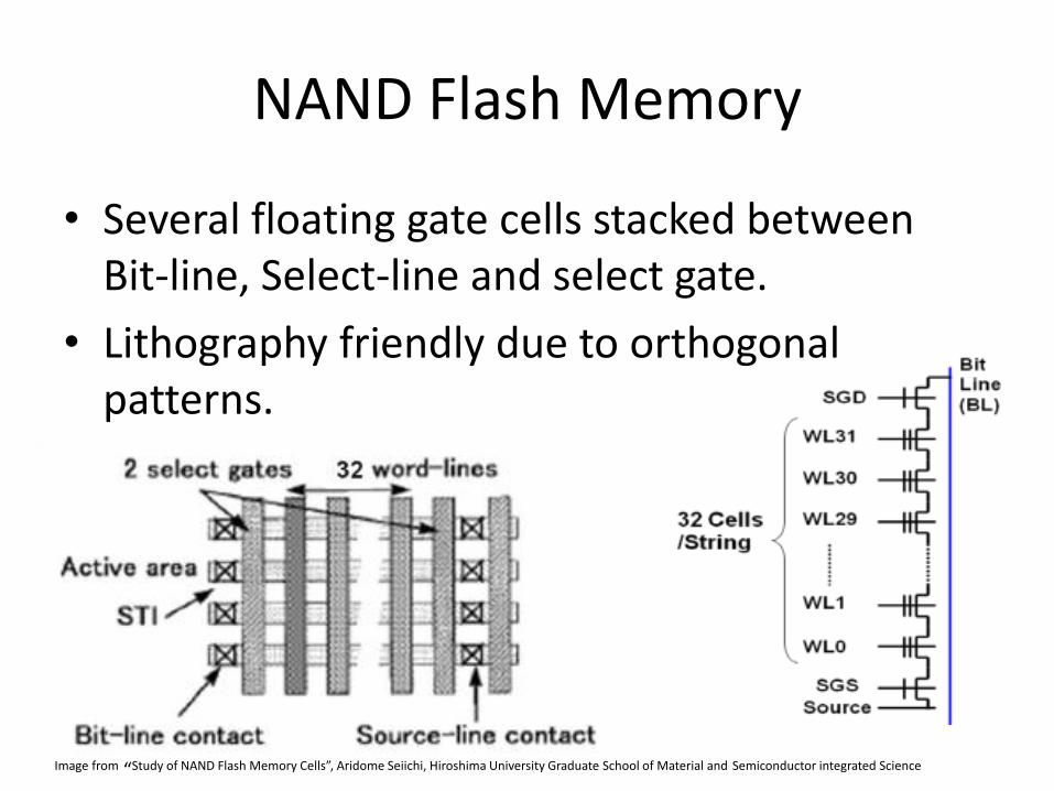
NAND Flash Memory
• Several floating gate cells stacked between Bit-line, Select-line and select gate.
• Lithography friendly due to orthogonal patterns.
Image from “Study of NAND Flash Memory Cells”, Aridome Seiichi, Hiroshima University Graduate School of Material and Semiconductor integrated Science
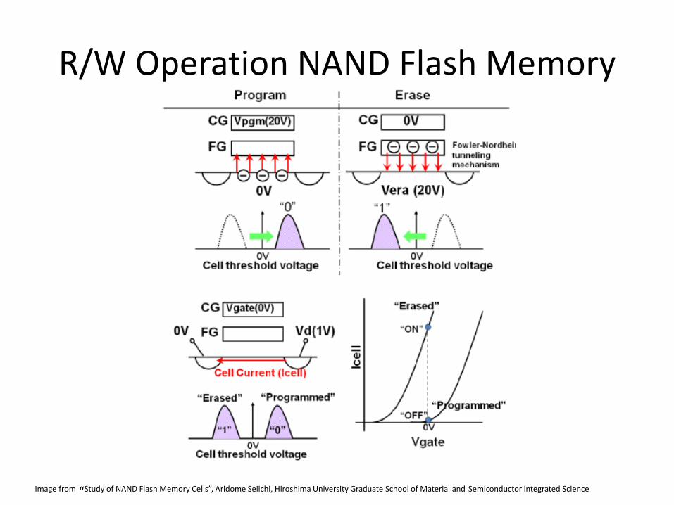
R/W Operation NAND Flash Memory
Image from “Study of NAND Flash Memory Cells”, Aridome Seiichi, Hiroshima University Graduate School of Material and Semiconductor integrated Science
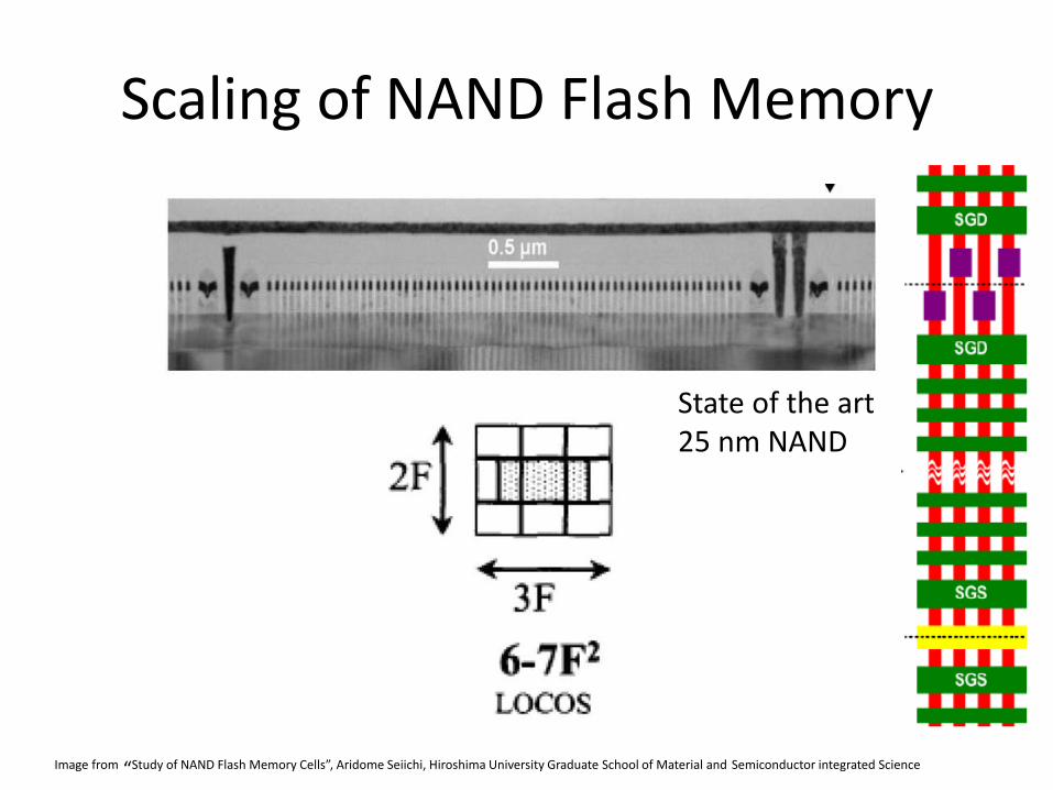
Scaling of NAND Flash Memory
State of the art 25 nm NAND
Image from “Study of NAND Flash Memory Cells”, Aridome Seiichi, Hiroshima University Graduate School of Material and Semiconductor integrated Science
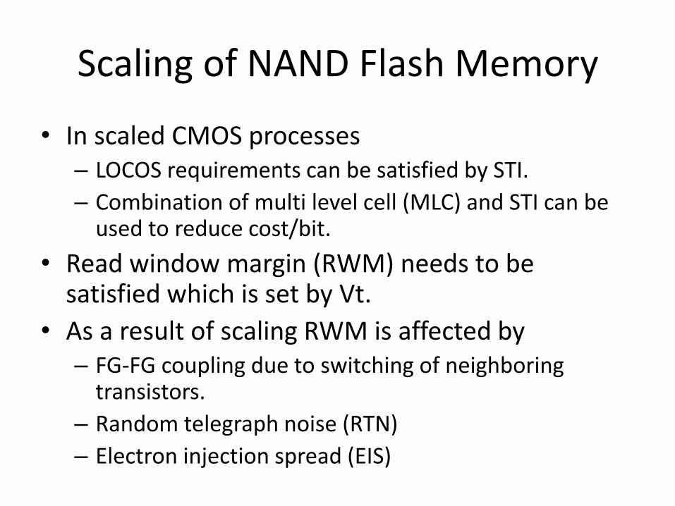
Scaling of NAND Flash Memory
• In scaled CMOS processes – LOCOS requirements can be satisfied by STI.
– Combination of multi level cell (MLC) and STI can be used to reduce cost/bit.
• Read window margin (RWM) needs to be satisfied which is set by Vt.
• As a result of scaling RWM is affected by – FG-FG coupling due to switching of neighboring
transistors.
– Random telegraph noise (RTN)
– Electron injection spread (EIS)
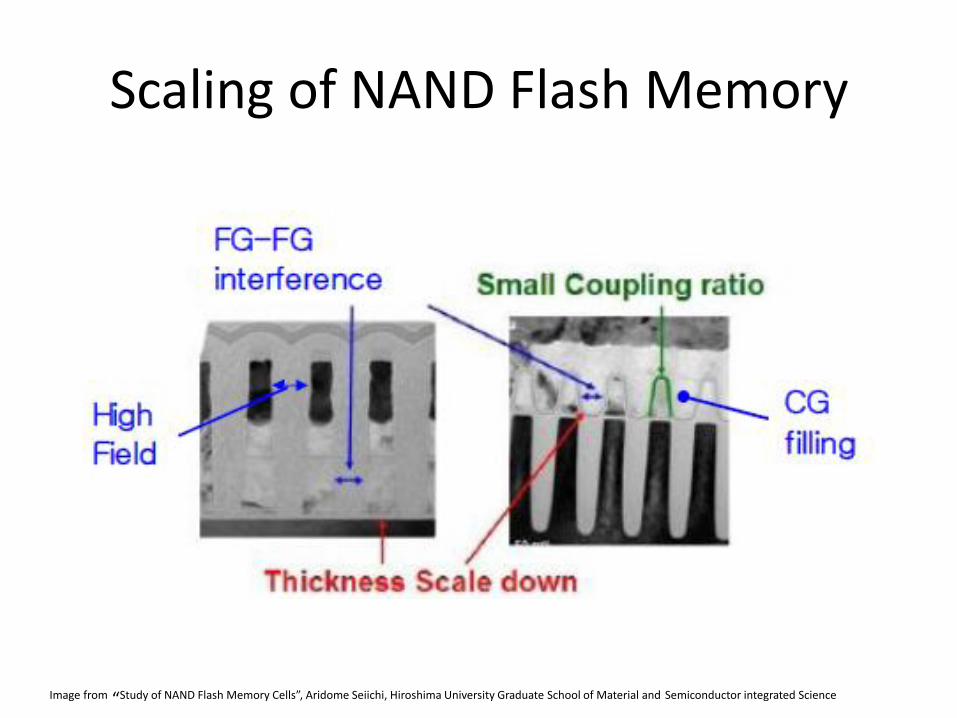
Scaling of NAND Flash Memory
Image from “Study of NAND Flash Memory Cells”, Aridome Seiichi, Hiroshima University Graduate School of Material and Semiconductor integrated Science
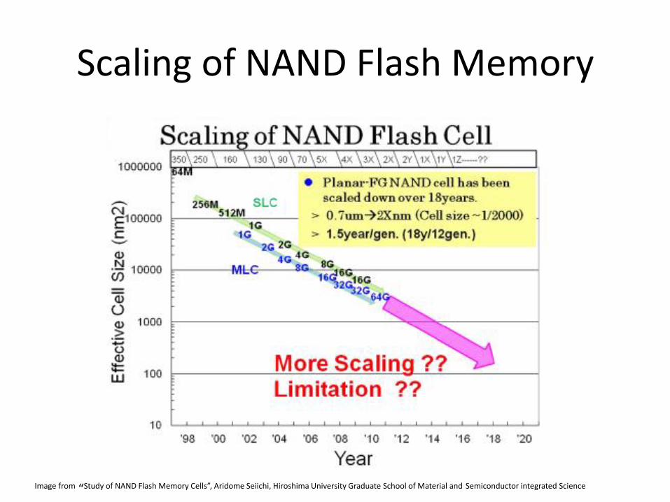
Scaling of NAND Flash Memory
Image from “Study of NAND Flash Memory Cells”, Aridome Seiichi, Hiroshima University Graduate School of Material and Semiconductor integrated Science
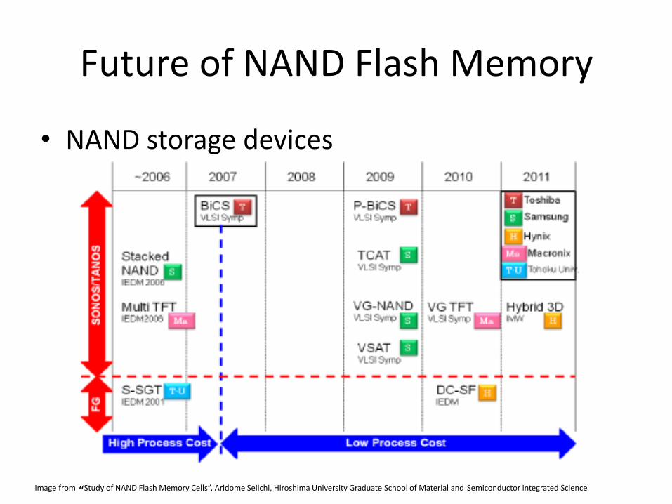
Future of NAND Flash Memory
• NAND storage devices
Image from “Study of NAND Flash Memory Cells”, Aridome Seiichi, Hiroshima University Graduate School of Material and Semiconductor integrated Science
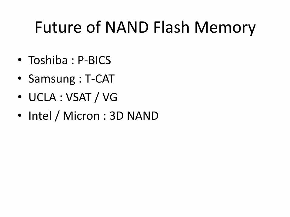
Future of NAND Flash Memory
• Toshiba : P-BICS
• Samsung : T-CAT
• UCLA : VSAT / VG
• Intel / Micron : 3D NAND
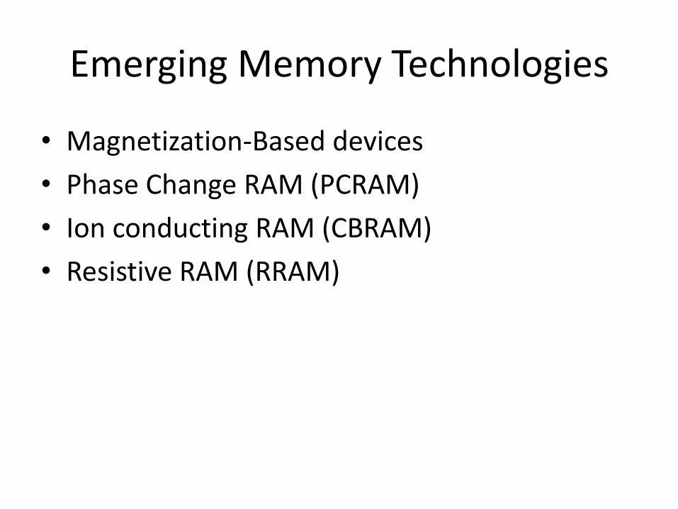
Emerging Memory Technologies
• Magnetization-Based devices
• Phase Change RAM (PCRAM)
• Ion conducting RAM (CBRAM)
• Resistive RAM (RRAM)
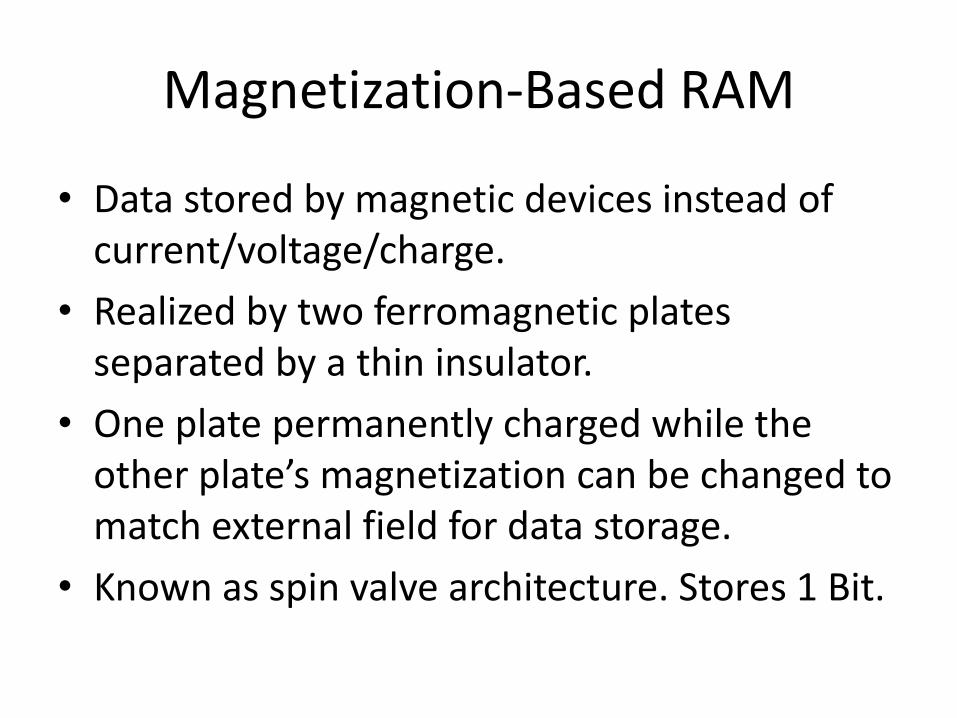
Magnetization-Based RAM
• Data stored by magnetic devices instead of current/voltage/charge.
• Realized by two ferromagnetic plates separated by a thin insulator.
• One plate permanently charged while the other plate’s magnetization can be changed to match external field for data storage.
• Known as spin valve architecture. Stores 1 Bit.
Magnetization-Based RAM
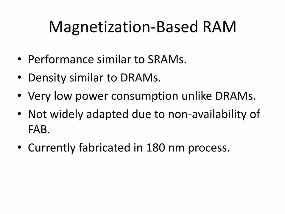
• Performance similar to SRAMs.
• Density similar to DRAMs.
• Very low power consumption unlike DRAMs.
• Not widely adapted due to non-availability of FAB.
• Currently fabricated in 180 nm process.
Phase Change RAM (PCRAM)
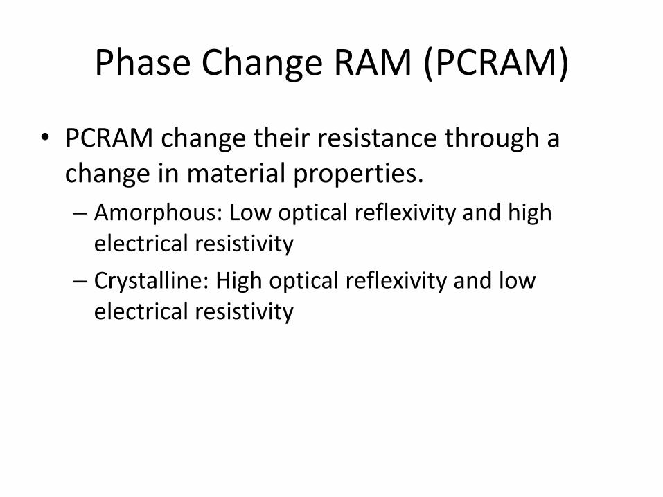
• PCRAM change their resistance through a change in material properties.
– Amorphous: Low optical reflexivity and high electrical resistivity
– Crystalline: High optical reflexivity and low electrical resistivity
Phase Change RAM (PCRAM)
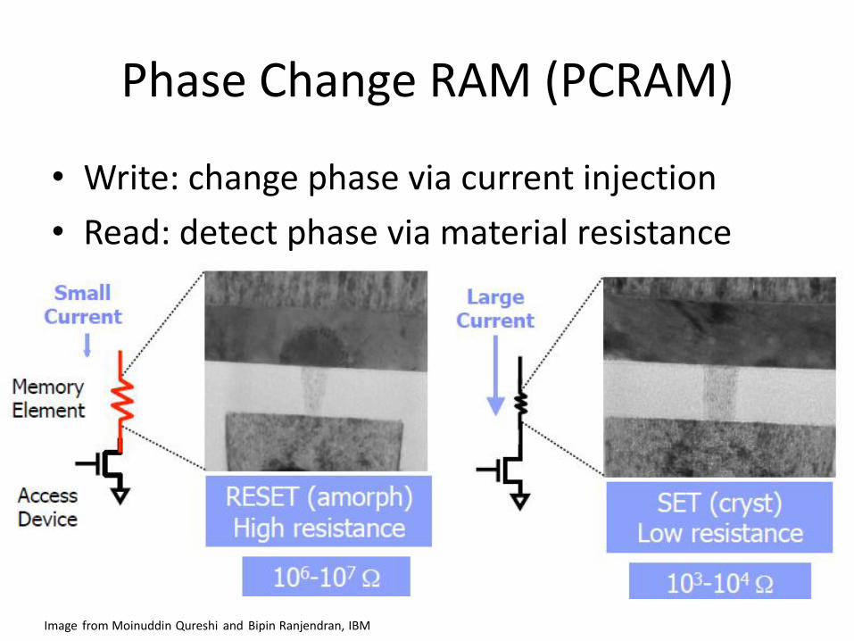
• Write: change phase via current injection
• Read: detect phase via material resistance
Image from Moinuddin Qureshi and Bipin Ranjendran, IBM
Phase Change RAM (PCRAM)
• Scales better than DRAM, Flash – Expected to scale to 9nm (2022 [ITRS])
– Prototyped at 20nm (Raoux+, IBM JRD 2008)
• Can be denser than DRAM – Prototypes with 2 bits/cell in ISSCC’08,
– 4 bits/cell by 2012
• Non-volatile – Retain data for >10 years at 85C
• No refresh needed, low idle power
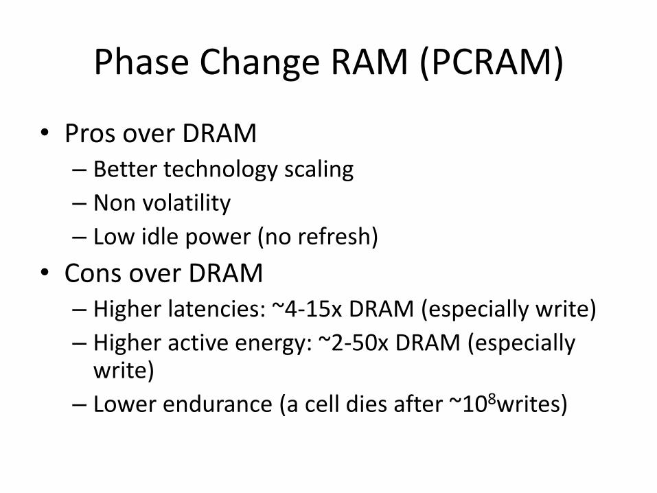
Phase Change RAM (PCRAM)
• Pros over DRAM – Better technology scaling
– Non volatility
– Low idle power (no refresh)
• Cons over DRAM – Higher latencies: ~4-15x DRAM (especially write)
– Higher active energy: ~2-50x DRAM (especially write)
– Lower endurance (a cell dies after ~108writes)
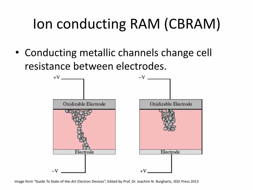
Ion conducting RAM (CBRAM)
• Conducting metallic channels change cell resistance between electrodes.
Image form “Guide To State-of-the-Art Electron Devices”, Edited by Prof. Dr. Joachim N. Burghartz, IEEE Press 2013
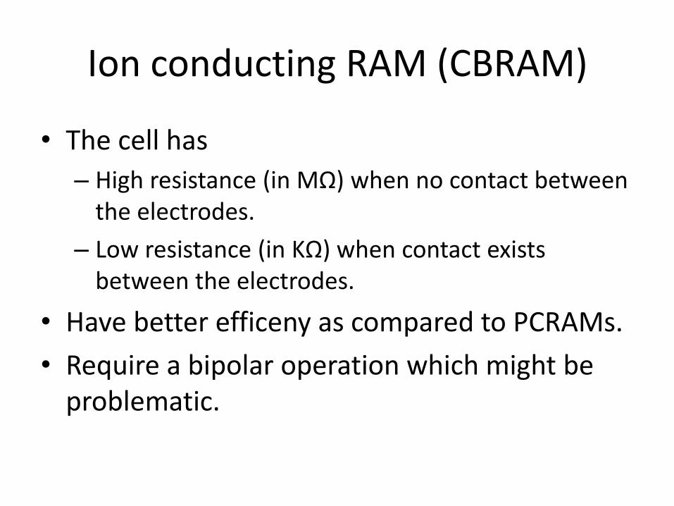
Ion conducting RAM (CBRAM)
• The cell has
– High resistance (in MΩ) when no contact between the electrodes.
– Low resistance (in KΩ) when contact exists between the electrodes.
• Have better efficeny as compared to PCRAMs.
• Require a bipolar operation which might be problematic.
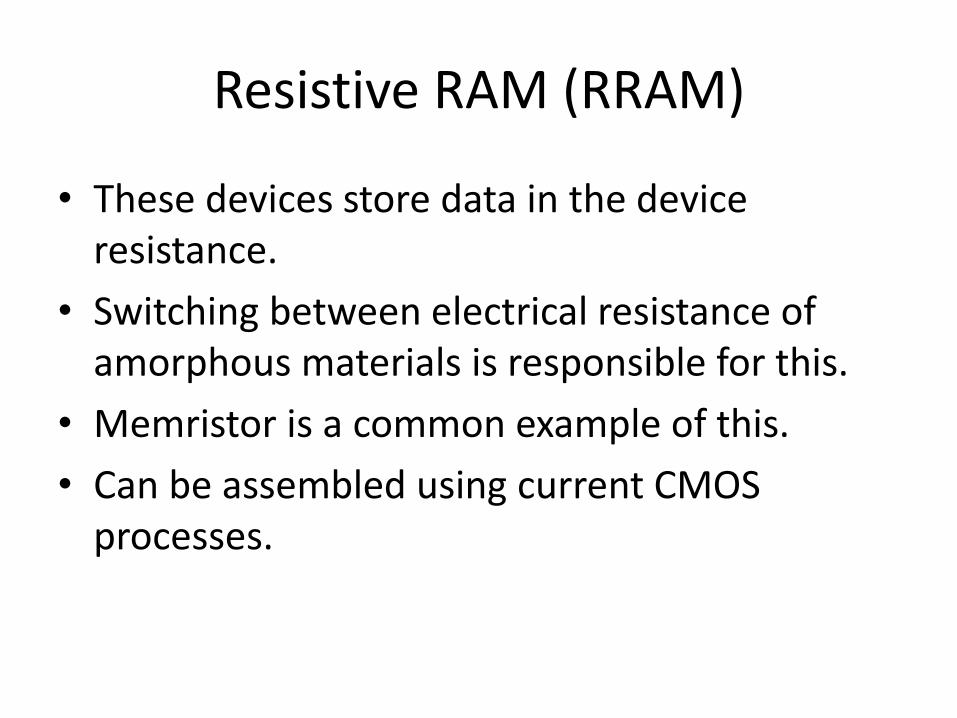
Resistive RAM (RRAM)
• These devices store data in the device resistance.
• Switching between electrical resistance of amorphous materials is responsible for this.
• Memristor is a common example of this.
• Can be assembled using current CMOS processes.
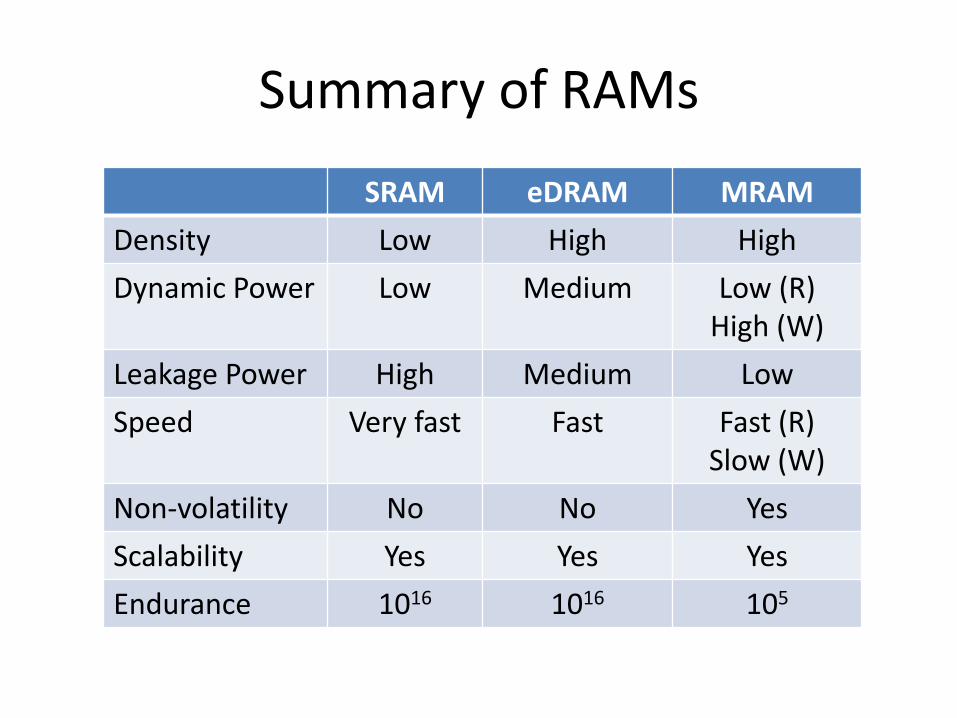
Summary of RAMs
SRAM eDRAM MRAM
Density Low High High
Dynamic Power Low Medium Low (R) High (W)
Leakage Power High Medium Low
Speed Very fast Fast Fast (R) Slow (W)
Non-volatility No No Yes
Scalability Yes Yes Yes
Endurance 1016 1016 105
Memristors
Memristors
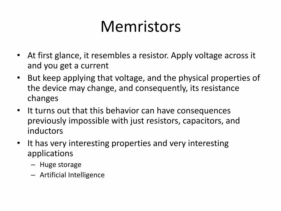
• At first glance, it resembles a resistor. Apply voltage across it and you get a current
• But keep applying that voltage, and the physical properties of the device may change, and consequently, its resistance changes
• It turns out that this behavior can have consequences previously impossible with just resistors, capacitors, and inductors
• It has very interesting properties and very interesting applications – Huge storage
– Artificial Intelligence
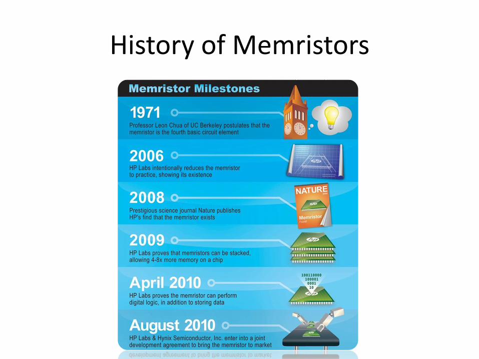
History of Memristors
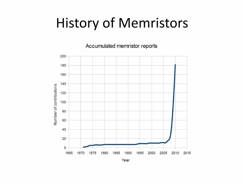
History of Memristors
Memristors
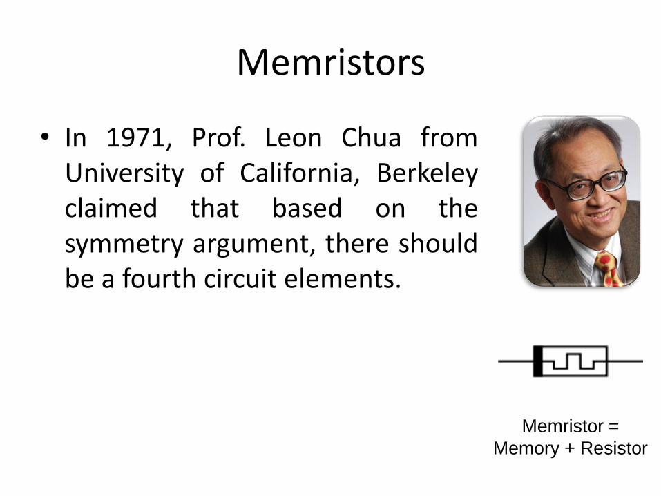
• In 1971, Prof. Leon Chua from University of California, Berkeley claimed that based on the symmetry argument, there should be a fourth circuit elements.
Memristor =
Memory + Resistor
Memristors
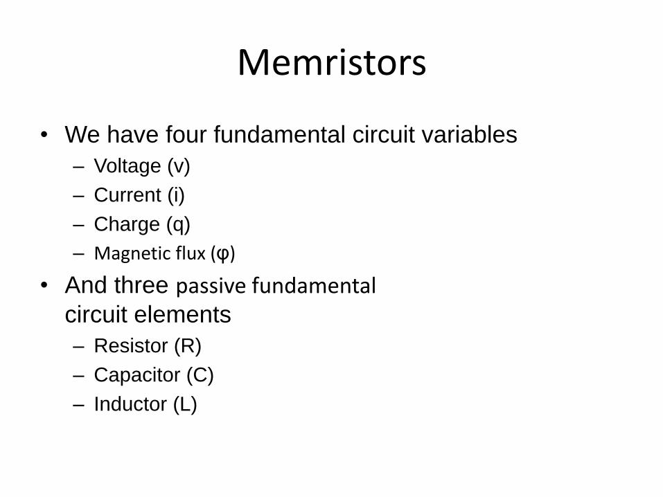
• We have four fundamental circuit variables
– Voltage (v)
– Current (i)
– Charge (q)
– Magnetic flux (φ)
• And three passive fundamental circuit elements
– Resistor (R)
– Capacitor (C)
– Inductor (L)
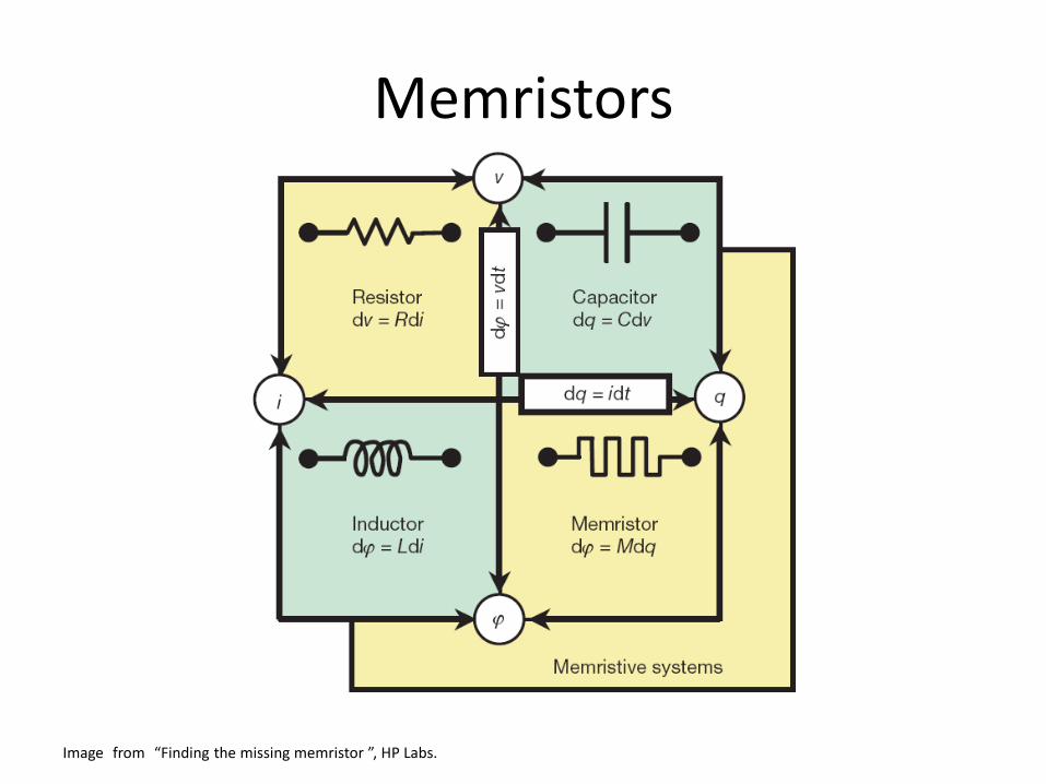
Memristors
Image from “Finding the missing memristor ”, HP Labs.
Memristors
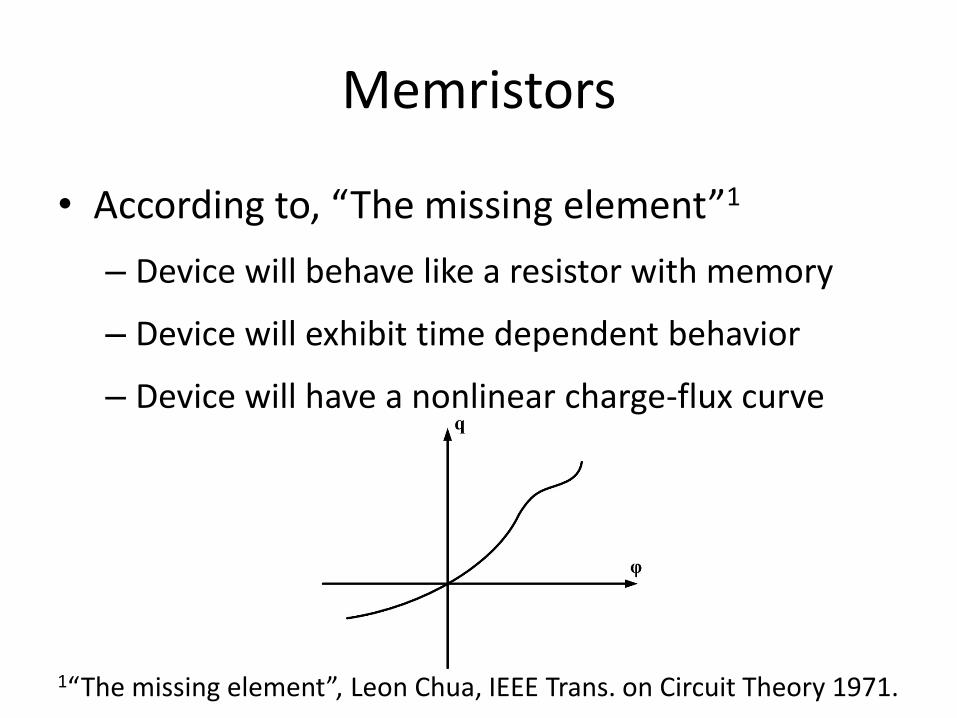
• According to, “The missing element”1
– Device will behave like a resistor with memory
– Device will exhibit time dependent behavior
– Device will have a nonlinear charge-flux curve
1“The missing element”, Leon Chua, IEEE Trans. on Circuit Theory 1971.
Memristors
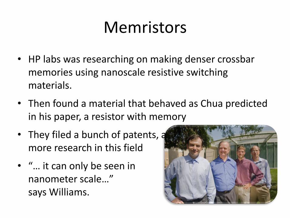
• HP labs was researching on making denser crossbar memories using nanoscale resistive switching materials.
• Then found a material that behaved as Chua predicted in his paper, a resistor with memory
• They filed a bunch of patents, and started conducting more research in this field
• “… it can only be seen in nanometer scale…” says Williams.
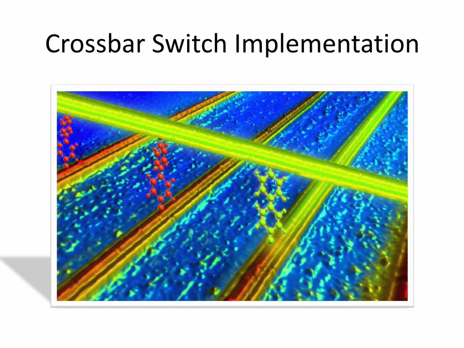
Crossbar Switch Implementation
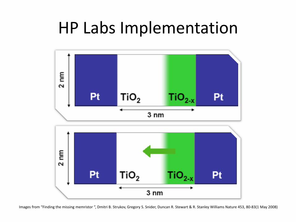
HP Labs Implementation
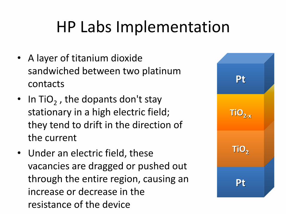
• A layer of titanium dioxide sandwiched between two platinum contacts
• In TiO2 , the dopants don't stay stationary in a high electric field; they tend to drift in the direction of the current
• Under an electric field, these vacancies are dragged or pushed out through the entire region, causing an increase or decrease in the resistance of the device
Pt
TiO2
TiO2-x
Pt
HP Labs Implementation
Images from “Finding the missing memristor ”, Dmitri B. Strukov, Gregory S. Snider, Duncan R. Stewart & R. Stanley Williams Nature 453, 80-83(1 May 2008)

Simplified Model
• Can be thought of a pipe that expands or
shrinks when water flows through it.
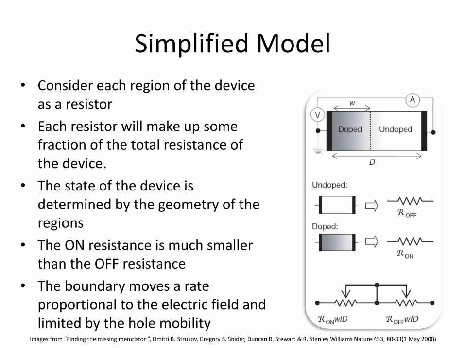
Simplified Model
• Consider each region of the device as a resistor
• Each resistor will make up some fraction of the total resistance of the device.
• The state of the device is determined by the geometry of the regions
• The ON resistance is much smaller than the OFF resistance
• The boundary moves a rate proportional to the electric field and limited by the hole mobility
Images from “Finding the missing memristor ”, Dmitri B. Strukov, Gregory S. Snider, Duncan R. Stewart & R. Stanley Williams Nature 453, 80-83(1 May 2008)
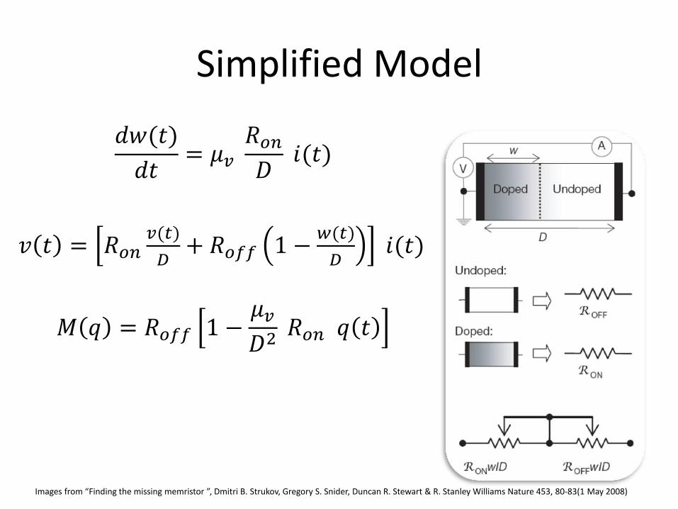
Simplified Model
𝑑𝑤(𝑡)
𝑑𝑡= 𝜇𝑣 𝑅𝑜𝑛𝐷 𝑖(𝑡)
𝑣 𝑡 = 𝑅𝑜𝑛𝑣(𝑡)
𝐷+ 𝑅𝑜𝑓𝑓 1 −
𝑤(𝑡)
𝐷 𝑖(𝑡)
𝑀 𝑞 = 𝑅𝑜𝑓𝑓 1 −𝜇𝑣𝐷2 𝑅𝑜𝑛 𝑞 𝑡
Images from “Finding the missing memristor ”, Dmitri B. Strukov, Gregory S. Snider, Duncan R. Stewart & R. Stanley Williams Nature 453, 80-83(1 May 2008)
Simplified Model
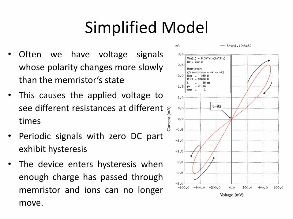
• Often we have voltage signals
whose polarity changes more slowly
than the memristor’s state
• This causes the applied voltage to
see different resistances at different
times
• Periodic signals with zero DC part
exhibit hysteresis
• The device enters hysteresis when
enough charge has passed through
memristor and ions can no longer
move.
Parameters affecting behavior of Memristors
• Different parameters can be tweaked
– Initial state
– Frequency
– Length/duration of the input
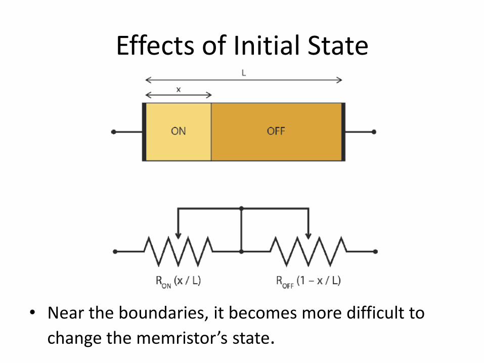
Effects of Initial State
• Near the boundaries, it becomes more difficult to
change the memristor’s state.
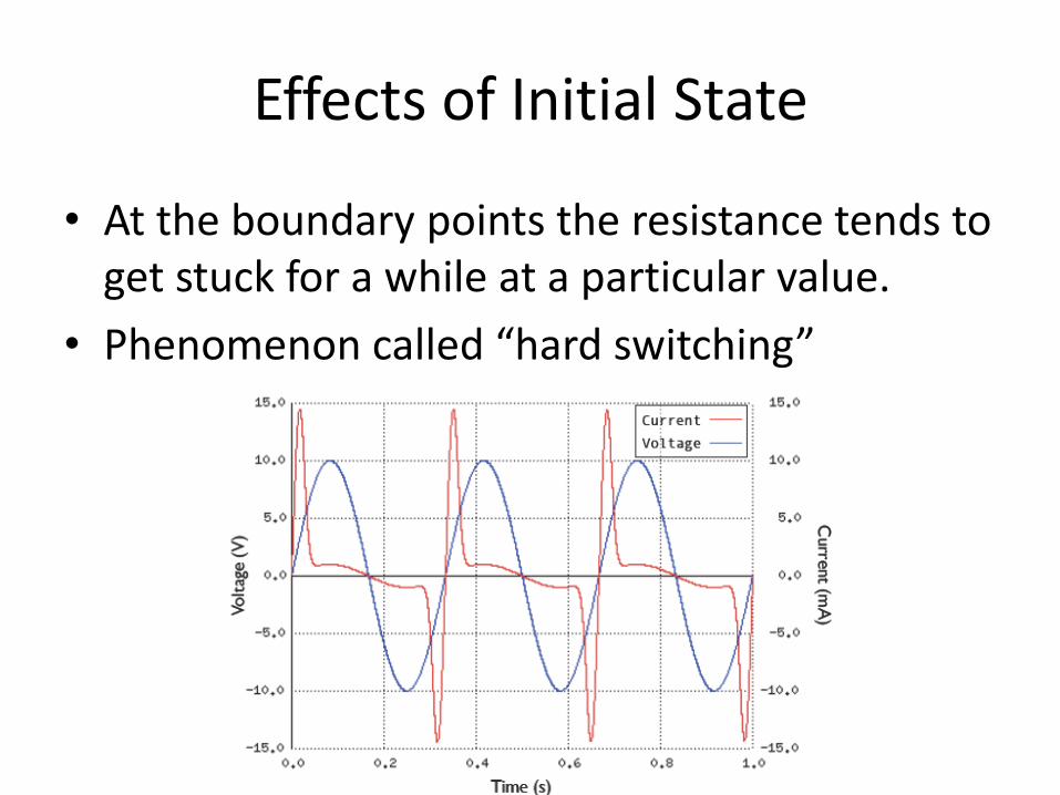
Effects of Initial State
• At the boundary points the resistance tends to get stuck for a while at a particular value.
• Phenomenon called “hard switching”
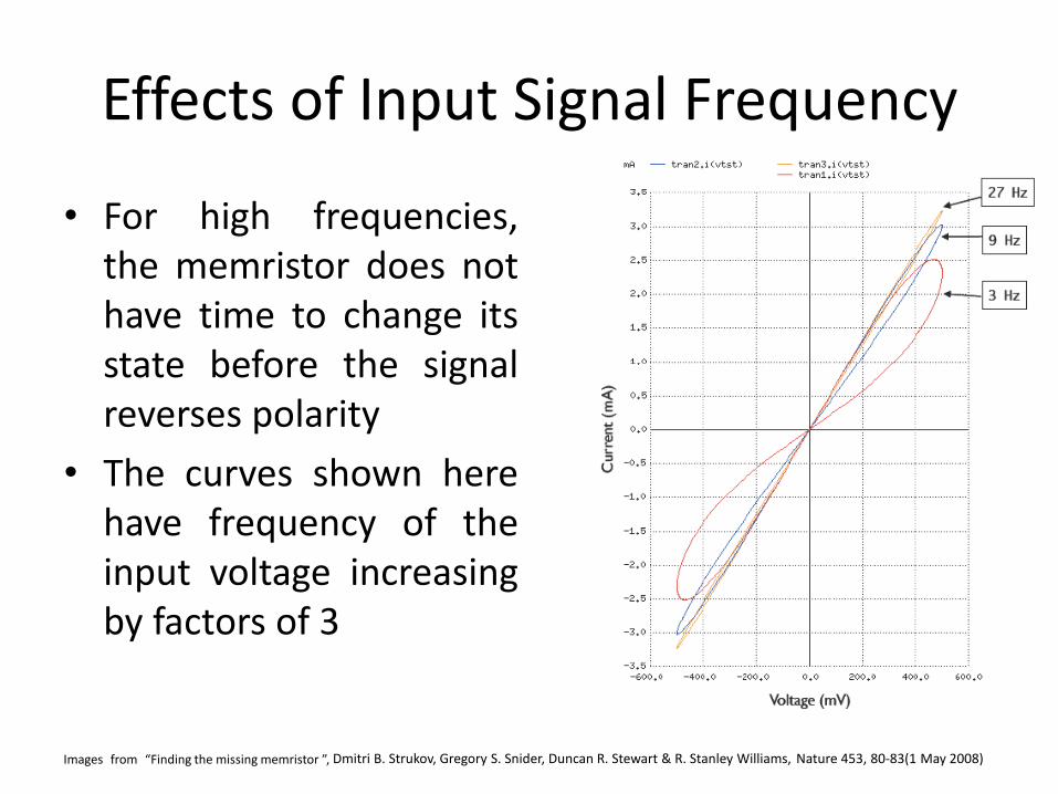
Effects of Input Signal Frequency
• For high frequencies, the memristor does not have time to change its state before the signal reverses polarity
• The curves shown here have frequency of the input voltage increasing by factors of 3
Images from “Finding the missing memristor ”, Dmitri B. Strukov, Gregory S. Snider, Duncan R. Stewart & R. Stanley Williams, Nature 453, 80-83(1 May 2008)
What are Memristor, Memcapacitor and Meminductor?
Yin, Z.; Tian, H.; Chen, G.; Chua, L.O., Circuits and Systems II: Express Briefs,
IEEE Transactions on , vol.62, no.4, pp.402,406, April 2015
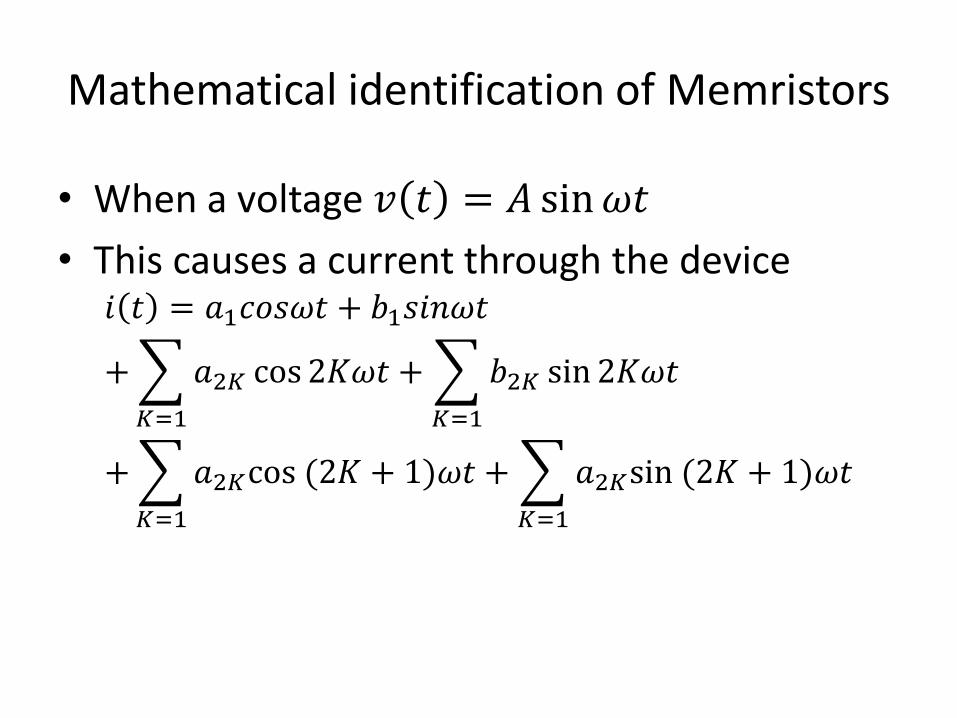
Mathematical identification of Memristors
• When a voltage 𝑣 𝑡 = 𝐴 sin𝜔𝑡
• This causes a current through the device 𝑖 𝑡 = 𝑎1𝑐𝑜𝑠𝜔𝑡 + 𝑏1𝑠𝑖𝑛𝜔𝑡
+ 𝑎2𝐾 cos 2𝐾𝜔𝑡
𝐾=1
+ 𝑏2𝐾 sin 2𝐾𝜔𝑡
𝐾=1
+ 𝑎2𝐾cos (2𝐾 + 1)𝜔𝑡
𝐾=1
+ 𝑎2𝐾sin (2𝐾 + 1)𝜔𝑡
𝐾=1
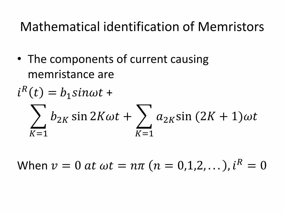
Mathematical identification of Memristors
• The components of current causing memristance are
𝑖𝑅 𝑡 = 𝑏1𝑠𝑖𝑛𝜔𝑡 +
𝑏2𝐾 sin 2𝐾𝜔𝑡
𝐾=1
+ 𝑎2𝐾sin (2𝐾 + 1)𝜔𝑡
𝐾=1
When 𝑣 = 0 𝑎𝑡 𝜔𝑡 = 𝑛𝜋 𝑛 = 0,1,2, . . . , 𝑖𝑅 = 0
Mathematical identification of Memristors
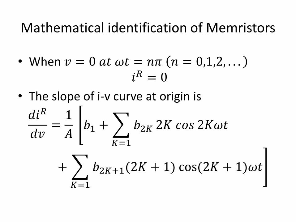
• When 𝑣 = 0 𝑎𝑡 𝜔𝑡 = 𝑛𝜋 𝑛 = 0,1,2, . . . 𝑖𝑅 = 0
• The slope of i-v curve at origin is
𝑑𝑖𝑅
𝑑𝑣=1
𝐴 𝑏1 + 𝑏2𝐾 2𝐾 𝑐𝑜𝑠 2𝐾𝜔𝑡
𝐾=1
+ 𝑏2𝐾+1(2𝐾 + 1) cos (2𝐾 + 1)𝜔𝑡
𝐾=1
Mathematical identification of Memristors
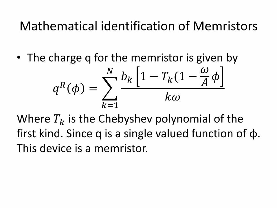
• The charge q for the memristor is given by
𝑞𝑅 𝜙 = 𝑏𝑘 1 − 𝑇𝑘(1 −
𝜔𝐴𝜙
𝑘𝜔
𝑁
𝑘=1
Where 𝑇𝑘 is the Chebyshev polynomial of the first kind. Since q is a single valued function of φ. This device is a memristor.
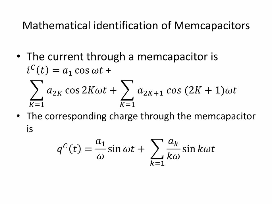
Mathematical identification of Memcapacitors
• The current through a memcapacitor is 𝑖𝐶 𝑡 = 𝑎1 cos𝜔𝑡 +
𝑎2𝐾 cos 2𝐾𝜔𝑡
𝐾=1
+ 𝑎2𝐾+1 𝑐𝑜𝑠 (2𝐾 + 1)𝜔𝑡
𝐾=1
• The corresponding charge through the memcapacitor is
𝑞𝐶 𝑡 =𝑎1𝜔sin𝜔𝑡 +
𝑎𝑘𝑘𝜔sin 𝑘𝜔𝑡
𝑘=1
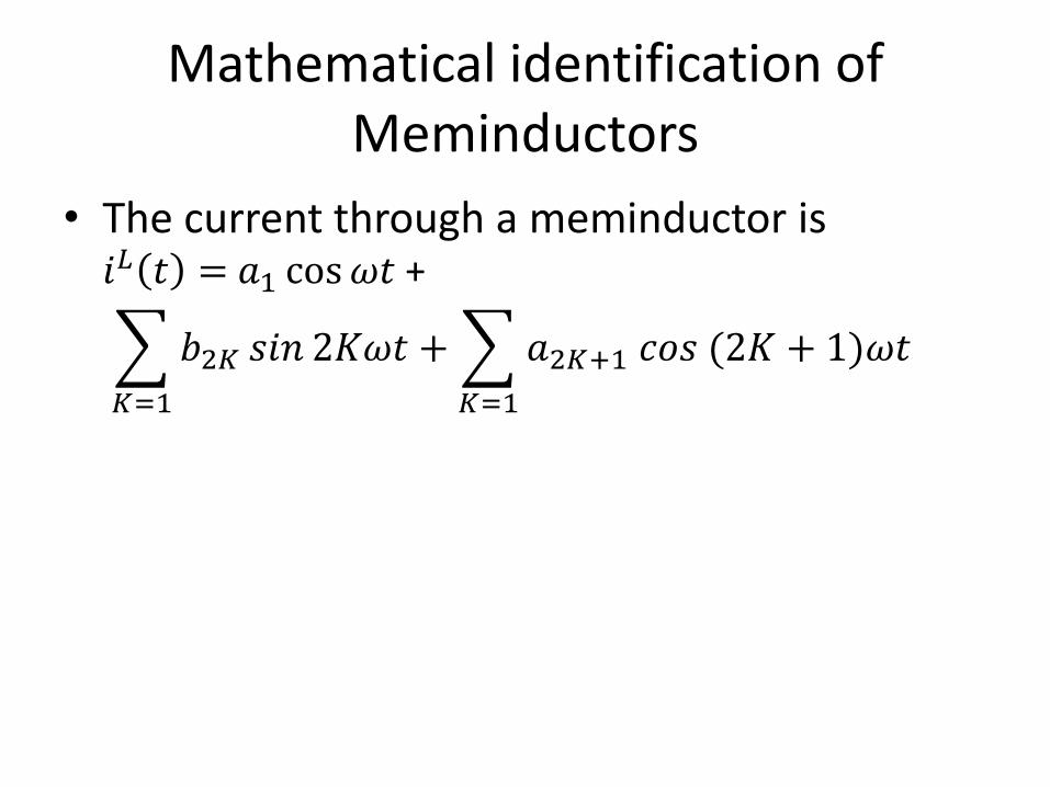
Mathematical identification of Meminductors
• The current through a meminductor is 𝑖𝐿 𝑡 = 𝑎1 cos𝜔𝑡 +
𝑏2𝐾 𝑠𝑖𝑛 2𝐾𝜔𝑡
𝐾=1
+ 𝑎2𝐾+1 𝑐𝑜𝑠 (2𝐾 + 1)𝜔𝑡
𝐾=1
Conclusion
• New memory technologies are currently an active area of research and will remain so in the near future.
• Focus is on technologies that can be fabricated using current CMOS technology.
• Memristors are an attractive alternative to SRAMs but there it needs a some time to introduce reliable memristors.