Embed Size (px)
Citation preview
1 PS8959B 10/01/09
ADVANCE INFORMATION - COMPANY CONFIDENTIAL
All trademarks are property of their respective owners.
PI3HDMI3013:1 Active Switch for HDMI™ Signals with Optimized
Equalization for Enhanced Signal Integrity
Features• Supply voltage, VDD = 3.3V ±5% • Each of the three input ports can support HDMI™ or DVI
signals• Supports both AC-coupled and DC-coupled inputs • Supports DeepColor™• High Performance, up to 2.5 Gbps per channel • Switching support for 3 side band signals
(SCL, SDA and HPD) • 5V Tolerance on all side band signals • SCL, SDA, and HPD pins are the only pins that can support
HOT INSERTION• Integrated 50-ohm (±10%) termination resistors at each high
speed signal input • TMDS input termination control on all high speed inputs• HDCP reset circuitry for quick communication when
switching from one port to another• Confi gurable output swing control • Confi gurable Pre-Emphasis levels • Confi gurable De-Emphasis • Optimized Equalization Single default setting will support all cable lengths• 8kV Contact ESD protection on all input data/clock channels
per IEC61000-4-2• Propagation delay ≤ 2ns • High Impedance Outputs when disabled • Packaging (Pb-free & Green): − 80-pin LQFP (FF80) − 64-pin TQFN (ZL64)
DescriptionPericom Semiconductor’s PI3HDMI301 3:1 active switch circuit is targeted for high-resolution video networks that are based on DVI/HDMI™ standards and TMDS signal processing. The PI3HDMI301 is an active 3 TMDS to 1 TMDS receiver switch with Hi-Z outputs. The device receives differential signals from selected video components and drives the video display unit. It provides controllable output swings, as well as provides a unique advanced pre-emphasis technique to increase rise and fall times which are reduced during transmission across long distances. Each complete HDMI/DVI channel also has slower speed, side band signals, that are required to be switched. Pericom’s solution provides a complete solution by integrating the side band switch together with the high speed switch in a single solution. Using Equalization at the input of each of the high speed channels, Pericom can successfully eliminate deterministic jitter caused by long cables from the source to the sink. The elimination of the deterministic jitter allows the user to use much longer cables (up to 25 meters).The maximum DVI/HDMI Bandwidth of 2.5 Gbps provides 36-bit Deep Color™ support, which is offered by HDMI™ revision 1.3. Due to its active uni-directional feature, this switch is designed for usage only for the video receiver’s side. For consumer video networks, the device sits at the receiver’s side to switch between multiple video components, such as PC, DVD, STB, D-VHS, etc. The PI3HDMI301 also provides enhanced robust ESD/EOS protection of 8kV, which is required by many consumer video networks today. The Optimized Equalization provides the user a single optimal setting that can provide passing results for HDMI jitter tests for all cable lengths: 1meter to 20meters with DeepColor support up to 36bits. Pericom also offers the ability to fi ne tune the equalization settings in situations where cable length is known. For example, if 25meter cable length is required, Pericom's solution can be adjusted to 16dB EQ to accept 25meter cable length.
09-0054
2 PS8959B 10/01/09
PI3HDMI3013:1 Active Switch for HDMI™ Signals with
Optimized Equalization for Enhanced Signal Integrity
ADVANCE INFORMATION - COMPANY CONFIDENTIAL
All trademarks are property of their respective owners.
Pin Confi guration (Top View)
1 2 3 4 5 6 7 8 9 10 1112 13141516 1718 19 20
4039383736353433323130292827262524232221
60 59585756 55 545352 515049 4847 46454443 42 416162636465666768697071727374757677787980
EQ
_S1
GN
D
EQ
_S0
D2+
3D
2-3
VD
DD
1+3
D1-
3G
ND
D0+
3D
0-3
VD
DC
LK+3
CLK
-3G
ND
SC
L3S
DA
3H
PD
3V
DD
OE
OC
_S3
SD
A1
OC
_S2
SC
L1G
ND
CLK
-1C
LK+1
VD
DD
0-1
D0+
1G
ND
D1-
1D
1+1
VD
DD
2-1
D2+
1G
ND
VD
DO
C_S
1O
C_S
0
VDDHPD2
HPD1
SDA2SCL2GNDGND
CLK-2CLK+2
VDDD0-2D0+2GNDD1-2D1+2VDDD2-2D2+2GNDVDD
HPD_SINKSDA_SINK
S2
SCL_SINKGNDGNDCLK-CLK+VDDD0-D0+GNDD1-D1+VDDD2-D2+GNDS3
S1
12345678910111213141516
17 18 19 20
60 59 58 57 56 55 54 53 52 51 50 49
S1
S2
S3
D2+
D2–
VD
DD
1+D
1–D
0+D
0–V
DD
CLK
+C
LK–
SC
L_S
INK
SD
A_S
INK
HP
D_S
INK
SDA1SCL1
CLK–1CLK+1
VDDD0–1D0+1D1–1D1+1VDD
D2–1D2+1VDD
OC-S1OC_S0OC_S2
21 22 23 24 25 26 27 28 29 30 31 32
48474645444342414039383736353433
64 63 62 61 D2+3D2–3VDDD1+3D1–3D0+3D0–3VDDCLK+3CLK–3SCL3SDA3HPD3VDDOEEQ_S0
OC
_S3
HP
D1
D2+
2D
2–2
VD
DD
1+2
D1–
2D
0+2
D0–
2V
DD
CLK
+2C
LK–2
SC
L2S
DA
2H
PD
2E
Q_S
1
GND
(Top View)
09-0054
3 PS8959B 10/01/09
PI3HDMI3013:1 Active Switch for HDMI™ Signals with
Optimized Equalization for Enhanced Signal Integrity
ADVANCE INFORMATION - COMPANY CONFIDENTIAL
All trademarks are property of their respective owners.
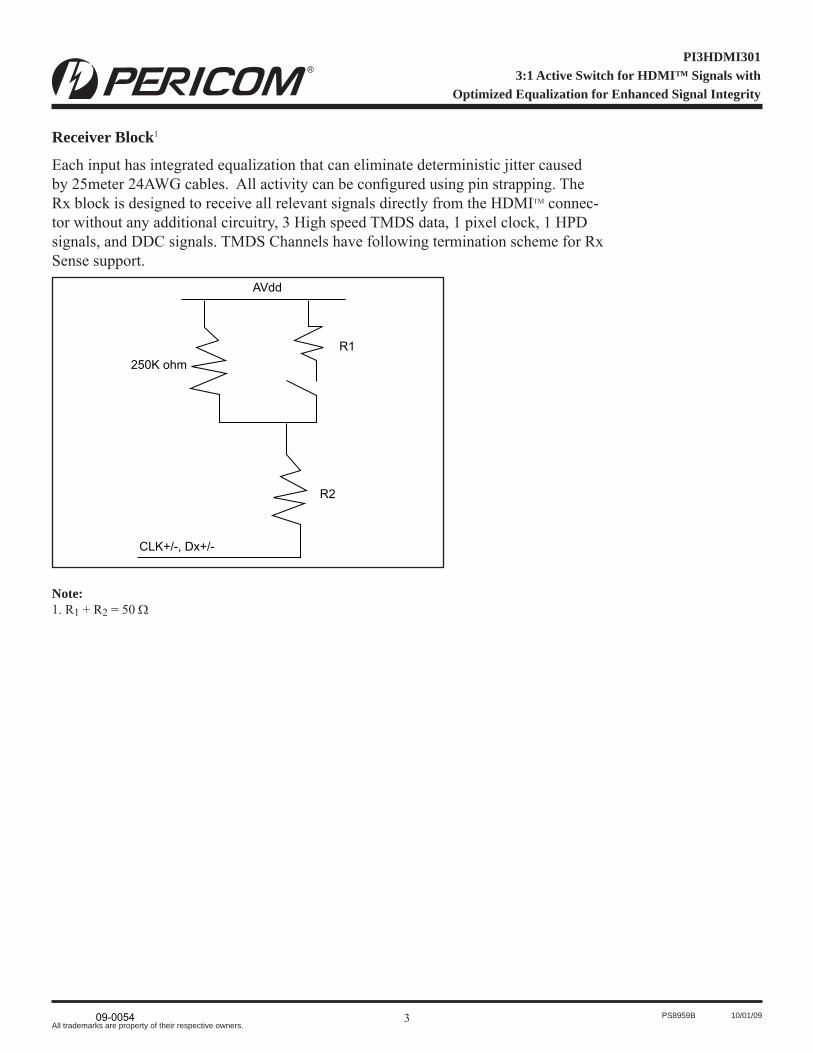
Receiver Block1
CLK+/-, Dx+/-
R2
250K�ohmR1
AVdd
Each input has integrated equalization that can eliminate deterministic jitter caused by 25meter 24AWG cables. All activity can be confi gured using pin strapping. The Rx block is designed to receive all relevant signals directly from the HDMITM connec-tor without any additional circuitry, 3 High speed TMDS data, 1 pixel clock, 1 HPD signals, and DDC signals. TMDS Channels have following termination scheme for Rx Sense support.
Note:1. R1 + R2 = 50
09-0054
4 PS8959B 10/01/09
PI3HDMI3013:1 Active Switch for HDMI™ Signals with
Optimized Equalization for Enhanced Signal Integrity
ADVANCE INFORMATION - COMPANY CONFIDENTIAL
All trademarks are property of their respective owners.
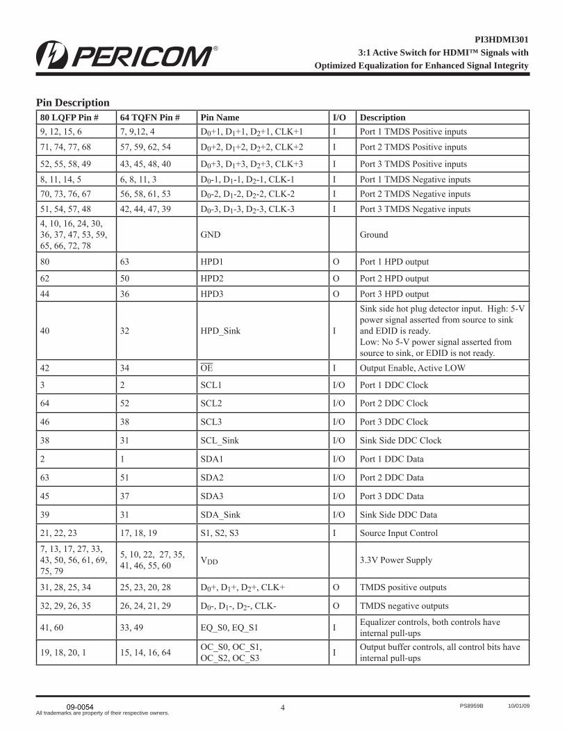
Pin Description80 LQFP Pin # 64 TQFN Pin # Pin Name I/O Description9, 12, 15, 6 7, 9,12, 4 D0+1, D1+1, D2+1, CLK+1 I Port 1 TMDS Positive inputs
71, 74, 77, 68 57, 59, 62, 54 D0+2, D1+2, D2+2, CLK+2 I Port 2 TMDS Positive inputs
52, 55, 58, 49 43, 45, 48, 40 D0+3, D1+3, D2+3, CLK+3 I Port 3 TMDS Positive inputs
8, 11, 14, 5 6, 8, 11, 3 D0-1, D1-1, D2-1, CLK-1 I Port 1 TMDS Negative inputs70, 73, 76, 67 56, 58, 61, 53 D0-2, D1-2, D2-2, CLK-2 I Port 2 TMDS Negative inputs 51, 54, 57, 48 42, 44, 47, 39 D0-3, D1-3, D2-3, CLK-3 I Port 3 TMDS Negative inputs 4, 10, 16, 24, 30, 36, 37, 47, 53, 59, 65, 66, 72, 78
GND Ground
80 63 HPD1 O Port 1 HPD output
62 50 HPD2 O Port 2 HPD output
44 36 HPD3 O Port 3 HPD output
40 32 HPD_Sink I
Sink side hot plug detector input. High: 5-V power signal asserted from source to sink and EDID is ready.Low: No 5-V power signal asserted from source to sink, or EDID is not ready.
42 34 OE I Output Enable, Active LOW
3 2 SCL1 I/O Port 1 DDC Clock
64 52 SCL2 I/O Port 2 DDC Clock
46 38 SCL3 I/O Port 3 DDC Clock
38 31 SCL_Sink I/O Sink Side DDC Clock
2 1 SDA1 I/O Port 1 DDC Data
63 51 SDA2 I/O Port 2 DDC Data
45 37 SDA3 I/O Port 3 DDC Data
39 31 SDA_Sink I/O Sink Side DDC Data
21, 22, 23 17, 18, 19 S1, S2, S3 I Source Input Control
7, 13, 17, 27, 33, 43, 50, 56, 61, 69, 75, 79
5, 10, 22, 27, 35, 41, 46, 55, 60 VDD 3.3V Power Supply
31, 28, 25, 34 25, 23, 20, 28 D0+, D1+, D2+, CLK+ O TMDS positive outputs
32, 29, 26, 35 26, 24, 21, 29 D0-, D1-, D2-, CLK- O TMDS negative outputs
41, 60 33, 49 EQ_S0, EQ_S1 I Equalizer controls, both controls have internal pull-ups
19, 18, 20, 1 15, 14, 16, 64 OC_S0, OC_S1, OC_S2, OC_S3 I Output buffer controls, all control bits have
internal pull-ups
09-0054
5 PS8959B 10/01/09
PI3HDMI3013:1 Active Switch for HDMI™ Signals with
Optimized Equalization for Enhanced Signal Integrity
ADVANCE INFORMATION - COMPANY CONFIDENTIAL
All trademarks are property of their respective owners.
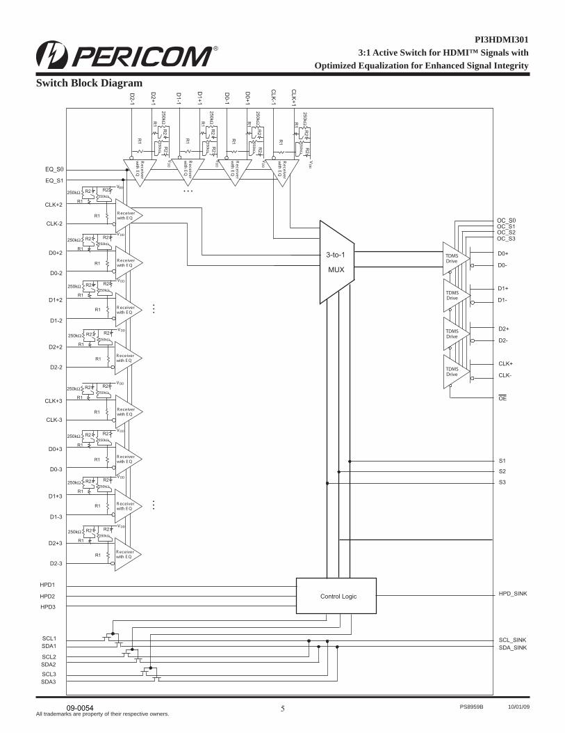
Switch Block Diagram
r e v i e c e R Q E h t i w
r e v i e c e R Q E h t i w
r e v i e c e R Q E h t i w
r e v i e c e R Q E h t i w
r e
v i
e c
e R
Q
E
h
t i
w
r e
v i
e c
e R
Q
E
h
t i
w
r e
v i
e c
e R
Q
E
h
t i
w D
DV
r e
v i
e c
e R
Q
E
h
t i
w
Control Logic
3-to-1
MUX
TDMS Drive
TDMS Drive
TDMS Drive
TDMS Drive
. . .
. . .
HPD1
HPD2
D0+
D0-
D1+
D1- D2+
D2-
CLK+
CLK-
OE
S1
HPD_SINK
SCL_SINK
SCL1SDA1
SCL2SDA2
SDA_SINK
OC_S1 OC_S2 OC_S3
EQ_S1
OC_S0
EQ_S0
R2
R2
250kΩR1
R1 250kΩ
D1-1
D1+1
D0+1
D0-1
CLK
+1
CLK
-1
D0+2
D0-2
D1+2
D1-2
D2+2
D2-2
DDVR2 R2250kΩ
R1
R1
250kΩ
CLK+2
CLK-2
D2-1
D2+1
S2
DD
VR
2R
2250kΩR
1
R1 250kΩ
DD
VR
2R
2250kΩR
1
R1 250kΩ
DD
VR
2R
2250kΩR
1
R1 250kΩ
DDVR2 R2250kΩ
R1
R1
250kΩ
DDVR2 R2250kΩ
R1
R1
250kΩ
DDVR2 R2250kΩ
R1
R1
250kΩ
S3
HPD3
SCL3SDA3
revieceRQE htiw
revieceRQE htiw
revieceRQE htiw
revieceRQE htiw
. . .
D0+3
D0-3
D1+3
D1-3
D2+3
D2-3
DDVR2 R2250kΩ
R1
R1
250kΩ
CLK+3
CLK-3
DDVR2 R2250kΩ
R1
R1
250kΩ
DDVR2 R2250kΩ
R1
R1
250kΩ
DDVR2 R2250kΩ
R1
R1
250kΩ
09-0054
6 PS8959B 10/01/09
PI3HDMI3013:1 Active Switch for HDMI™ Signals with
Optimized Equalization for Enhanced Signal Integrity
ADVANCE INFORMATION - COMPANY CONFIDENTIAL
All trademarks are property of their respective owners.
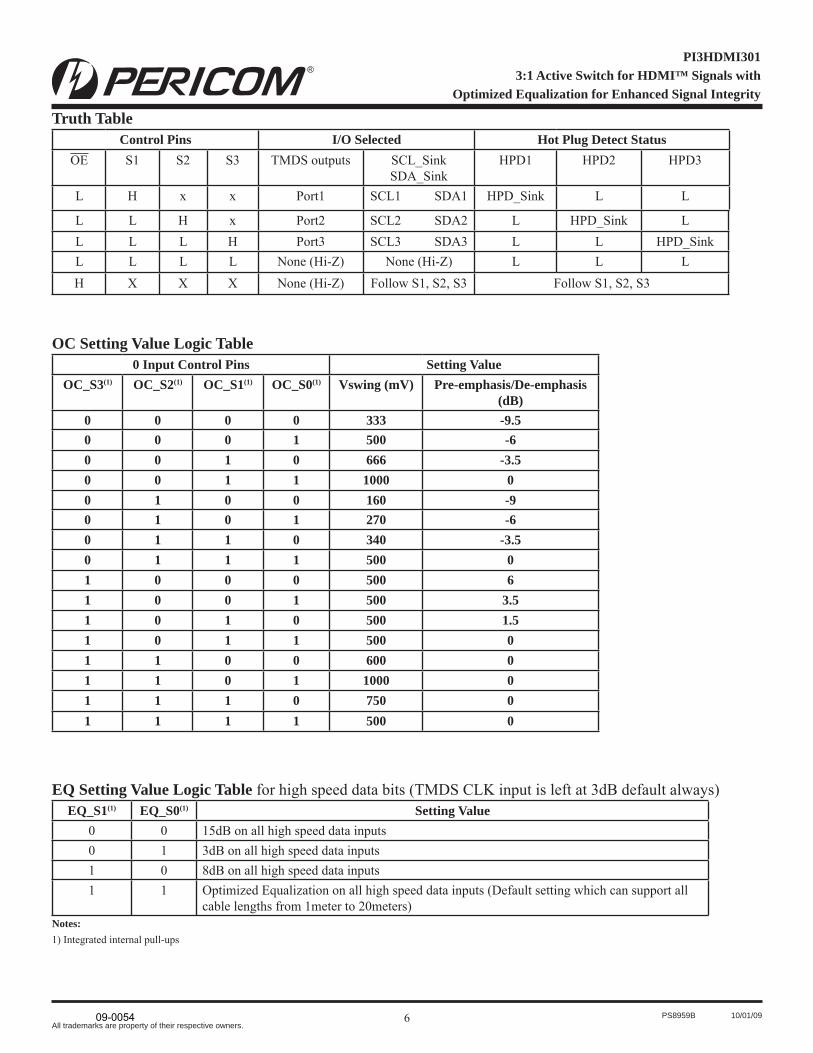
OC Setting Value Logic Table0 Input Control Pins Setting Value
OC_S3(1) OC_S2(1) OC_S1(1) OC_S0(1) Vswing (mV) Pre-emphasis/De-emphasis (dB)
0 0 0 0 333 -9.50 0 0 1 500 -60 0 1 0 666 -3.50 0 1 1 1000 00 1 0 0 160 -90 1 0 1 270 -60 1 1 0 340 -3.50 1 1 1 500 01 0 0 0 500 61 0 0 1 500 3.51 0 1 0 500 1.51 0 1 1 500 01 1 0 0 600 01 1 0 1 1000 01 1 1 0 750 01 1 1 1 500 0
EQ Setting Value Logic Table for high speed data bits (TMDS CLK input is left at 3dB default always)EQ_S1(1) EQ_S0(1) Setting Value
0 0 15dB on all high speed data inputs0 1 3dB on all high speed data inputs1 0 8dB on all high speed data inputs1 1 Optimized Equalization on all high speed data inputs (Default setting which can support all
cable lengths from 1meter to 20meters)Notes:1) Integrated internal pull-ups
Truth TableControl Pins I/O Selected Hot Plug Detect Status
OE S1 S2 S3 TMDS outputs SCL_Sink SDA_Sink
HPD1 HPD2 HPD3
L H x x Port1 SCL1 SDA1 HPD_Sink L L
L L H x Port2 SCL2 SDA2 L HPD_Sink LL L L H Port3 SCL3 SDA3 L L HPD_SinkL L L L None (Hi-Z) None (Hi-Z) L L LH X X X None (Hi-Z) Follow S1, S2, S3 Follow S1, S2, S3
09-0054
7 PS8959B 10/01/09
PI3HDMI3013:1 Active Switch for HDMI™ Signals with
Optimized Equalization for Enhanced Signal Integrity
ADVANCE INFORMATION - COMPANY CONFIDENTIAL
All trademarks are property of their respective owners.
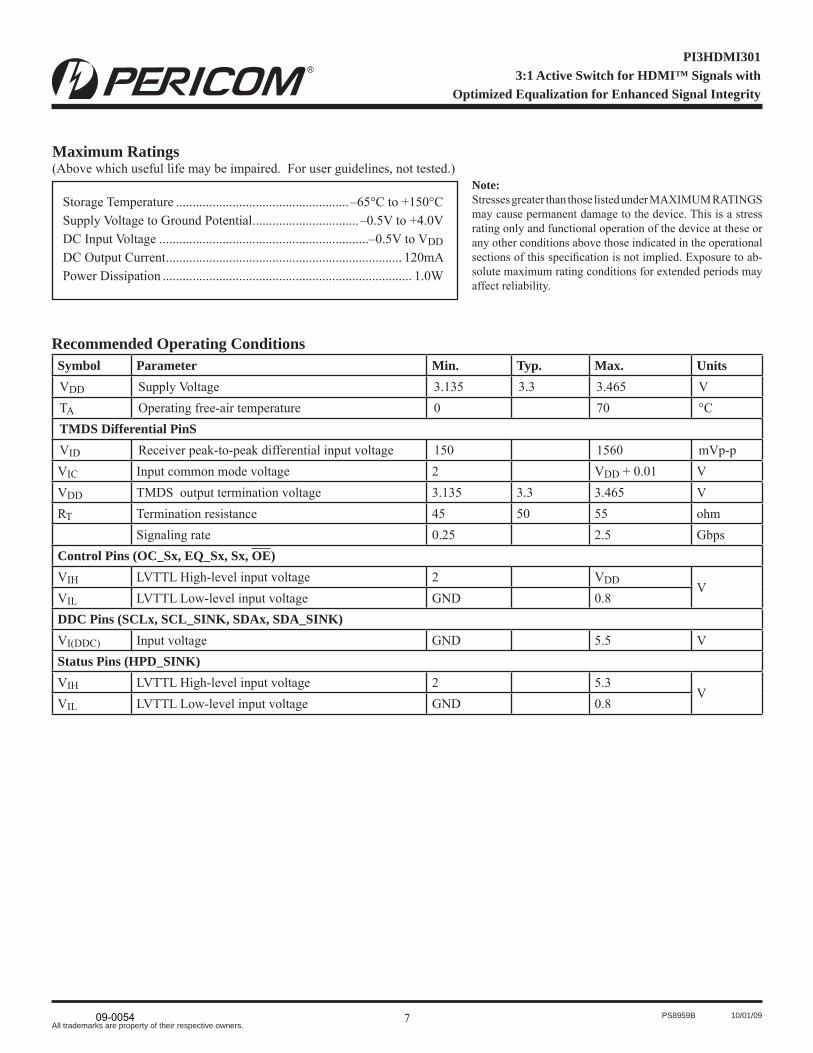
Storage Temperature .................................................... –65°C to +150°CSupply Voltage to Ground Potential ................................–0.5V to +4.0VDC Input Voltage ...............................................................–0.5V to VDDDC Output Current ....................................................................... 120mAPower Dissipation ........................................................................... 1.0W
Note:Stresses greater than those listed under MAX I MUM RAT INGS may cause permanent damage to the de vice. This is a stress rating only and func tion al op er a tion of the device at these or any other conditions above those indicated in the operational sections of this spec i fi ca tion is not implied. Exposure to ab-solute max i mum rating con di tions for extended periods may affect re li abil i ty.
Maximum Ratings(Above which useful life may be impaired. For user guide lines, not tested.)
Recommended Operating ConditionsSymbol Parameter Min. Typ. Max. UnitsVDD Supply Voltage 3.135 3.3 3.465 VTA Operating free-air temperature 0 70 °CTMDS Differential PinSVID Receiver peak-to-peak differential input voltage 150 1560 mVp-pVIC Input common mode voltage 2 VDD + 0.01 VVDD TMDS output termination voltage 3.135 3.3 3.465 VRT Termination resistance 45 50 55 ohm
Signaling rate 0.25 2.5 GbpsControl Pins (OC_Sx, EQ_Sx, Sx, OE)VIH LVTTL High-level input voltage 2 VDD VVIL LVTTL Low-level input voltage GND 0.8DDC Pins (SCLx, SCL_SINK, SDAx, SDA_SINK)VI(DDC) Input voltage GND 5.5 VStatus Pins (HPD_SINK)VIH LVTTL High-level input voltage 2 5.3
VVIL LVTTL Low-level input voltage GND 0.8
09-0054
8 PS8959B 10/01/09
PI3HDMI3013:1 Active Switch for HDMI™ Signals with
Optimized Equalization for Enhanced Signal Integrity
ADVANCE INFORMATION - COMPANY CONFIDENTIAL
All trademarks are property of their respective owners.
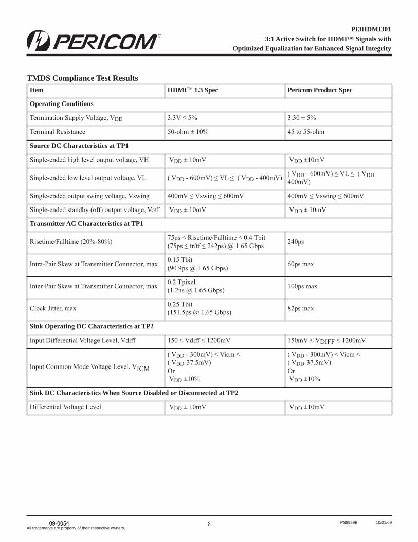
Item HDMITM 1.3 Spec Pericom Product Spec
Operating Conditions
Termination Supply Voltage, VDD 3.3V ≤ 5% 3.30 ± 5%
Terminal Resistance 50-ohm ± 10% 45 to 55-ohm
Source DC Characteristics at TP1
Single-ended high level output voltage, VH VDD ± 10mV VDD ±10mV
Single-ended low level output voltage, VL ( VDD - 600mV) ≤ VL ≤ ( VDD - 400mV) ( VDD - 600mV) ≤ VL ≤ ( VDD - 400mV)
Single-ended output swing voltage, Vswing 400mV ≤ Vswing ≤ 600mV 400mV ≤ Vswing ≤ 600mV
Single-ended standby (off) output voltage, Voff VDD ± 10mV VDD ± 10mV
Transmitter AC Characteristics at TP1
Risetime/Falltime (20%-80%) 75ps ≤ Risetime/Falltime ≤ 0.4 Tbit(75ps ≤ tr/tf ≤ 242ps) @ 1.65 Gbps 240ps
Intra-Pair Skew at Transmitter Connector, max 0.15 Tbit(90.9ps @ 1.65 Gbps) 60ps max
Inter-Pair Skew at Transmitter Connector, max 0.2 Tpixel(1.2ns @ 1.65 Gbps) 100ps max
Clock Jitter, max 0.25 Tbit(151.5ps @ 1.65 Gbps) 82ps max
Sink Operating DC Characteristics at TP2
Input Differential Voltage Level, Vdiff 150 ≤ Vdiff ≤ 1200mV 150mV ≤ VDIFF ≤ 1200mV
Input Common Mode Voltage Level, VICM
( VDD - 300mV) ≤ Vicm ≤ ( VDD-37.5mV) Or VDD ±10%
( VDD - 300mV) ≤ Vicm ≤ ( VDD-37.5mV) Or VDD ±10%
Sink DC Characteristics When Source Disabled or Disconnected at TP2
Differential Voltage Level VDD ± 10mV VDD ±10mV
TMDS Compliance Test Results
09-0054
9 PS8959B 10/01/09
PI3HDMI3013:1 Active Switch for HDMI™ Signals with
Optimized Equalization for Enhanced Signal Integrity
ADVANCE INFORMATION - COMPANY CONFIDENTIAL
All trademarks are property of their respective owners.
Electrical Characteristics (over recommended operating conditions unless otherwise noted)Symbol Parameter Test Conditions Min. Typ.(1) Max. Units
ICC Supply CurrentVIH = VDD, VIL = VDD - 0.4V, RT = 50-ohm, VDD = 3.3VData Input = 1.65 Gbps HDMITM data patternCLK Input = 165 MHz clock
200 mA
PD Power Dissipation 660 mW
ICCQ Standby Current OE = HIGH, S1 = S2 = S3 = LOW 8 mA
TMDS Differential Pins
VOHSingle-ended high-level output voltage
VDD = 3.3V, RT = 50-ohmPre-emphasis/De-emphasis = 0dB
VDD- 10
VDD + 10
mVVOLSingle-ended low-level output voltage
VDD - 600
VDD - 400
Vswing Single-ended output swing voltage 400 600
VOD(O)Overshoot of output differential voltage 6% 15%
2xVswingVOD(U)
Undershoot of output differential voltage 12% 25%
ΔVOC(SS)
Change in steady-state common-mode output voltage between logic states
0.5 5 mV
|I(OS)| Short circuit output current 12 mA
VODE(SS)Steady state output differential voltage
OC_Sx = GND, Data Input = 250 Mbps HDMITM data patternCLK Input = 25 MHz clockx = 0, 1, 2, 3
560 840mVp-p
VODE(PP)Peak-to-peak output differential voltage 800 1200
VI(open)Single-ended input voltage under high impedance input or open input II = 10μA VDD -
10 VDD + 10 mV
RINT Input termination resistance VIN = 2.9V 45 50 55 ohm
DDC I/O Pins (SCLx, SCL_SINK, SDAx, SDA_SINK)
|Ilkg| Input leakage currentVI = 5.5V -50 50
μAVI = VDD -10 10
CIO Input/output capacitance VI = 0V 7.5 pF
RON Switch resistance IO = 3mA, VO = 0.4V 25 50 ohm
VPASS Switch output voltage VI = 3.3V, II = 100μA 1.5(2) 2.0 2.5(3) V
Status Pins (HPD)
VOH(TTL) TTL High-level output voltage IOH = -4mA 2.4 V
VOL(TTL) TTL Low-level output voltage IOL = 4mA 0.4 V
(Table Continued)
09-0054
10 PS8959B 10/01/09
PI3HDMI3013:1 Active Switch for HDMI™ Signals with
Optimized Equalization for Enhanced Signal Integrity
ADVANCE INFORMATION - COMPANY CONFIDENTIAL
All trademarks are property of their respective owners.
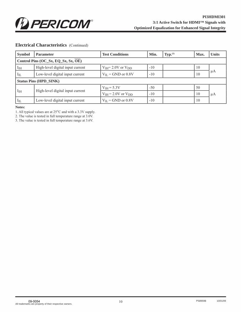
Symbol Parameter Test Conditions Min. Typ.(1) Max. Units
Control Pins (OC_Sx, EQ_Sx, Sx, OE)IIH High-level digital input current VIH= 2.0V or VDD -10 10
μAIIL Low-level digital input current VIL = GND or 0.8V -10 10
Status Pins (HPD_SINK)
IIH High-level digital input currentVIH = 5.3V -50 50
μAVIH = 2.0V or VDD -10 10IIL Low-level digital input current VIL = GND or 0.8V -10 10
Electrical Characteristics (Continued)
Notes:1. All typical values are at 25°C and with a 3.3V supply.2. The value is tested in full temperature range at 3.0V.3. The value is tested in full temperature range at 3.6V.
09-0054
11 PS8959B 10/01/09
PI3HDMI3013:1 Active Switch for HDMI™ Signals with
Optimized Equalization for Enhanced Signal Integrity
ADVANCE INFORMATION - COMPANY CONFIDENTIAL
All trademarks are property of their respective owners.
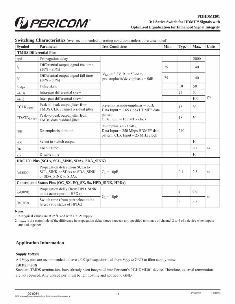
Switching Characteristics (over recommended operating conditions unless otherwise noted)Symbol Parameter Test Conditions Min. Typ.(1) Max. UnitsTMDS Differential Pinstpd Propagation delay
VDD = 3.3V, RT = 50-ohm, pre-emphasis/de-emphasis = 0dB
2000
ps
trDifferential output signal rise time (20% - 80%) 75 140
tfDifferential output signal fall time (20% - 80%) 75 140
tsk(p) Pulse skew 10 50tsk(D) Intra-pair differential skew 23 50tsk(o) Inter-pair differential skew(2) 100
TCLKjit(pp)Peak-to-peak output jitter from TMDS CLK channel residual jitter
pre-emphasis/de-emphasis = 0dB, Data Input = 1.65 Gbps HDMITM data patternCLK Input = 165 MHz clock
15 30
TDATAjit(pp)Peak-to-peak output jitter from TMDS data residual jitter 18 50
tDE De-emphasis durationde-emphasis = -3.5dB, Data Input = 250 Mbps HDMITM data pattern, CLK Input = 25 MHz clock
240
tSX Select to switch output 10
nsten Enable time 200
tdis Disable time 10
DDC I/O Pins (SCLx, SCL_SINK, SDAx, SDA_SINK)
tpd(DDC)
Propagation delay from SCLn to SCL_SINK or SDAx to SDA_SINK or SDA_SINK to SDAx
CL = 10pF 0.4 2.5 ns
Control and Status Pins (OC_SX, EQ_SX, Sx, HPD_SINK, HPDx)
tpd(HPD)Propagation delay (from HPD_SINK to the active port of HPDx)
CL = 10pF2 6.0
nstsx(HPD)
Switch time (from port select to the latest valid status of HPDx) 3 6.5
Notes:1. All typical values are at 25°C and with a 3.3V supply.2. tsk(o) is the magnitude of the difference in propagation delay times between any specifi ed terminals of channel 2 to 4 of a device when inputs are tied together.
Application Information
Supply VoltageAll VDD pins are recommended to have a 0.01μF capacitor tied from VDD to GND to fi lter supply noiseTMDS inputsStandard TMDS terminations have already been integrated into Pericom’s PI3HDMI301 device. Therefore, external terminations are not required. Any unused port must be left fl oating and not tied to GND.
09-0054
12 PS8959B 10/01/09
PI3HDMI3013:1 Active Switch for HDMI™ Signals with
Optimized Equalization for Enhanced Signal Integrity
ADVANCE INFORMATION - COMPANY CONFIDENTIAL
All trademarks are property of their respective owners.
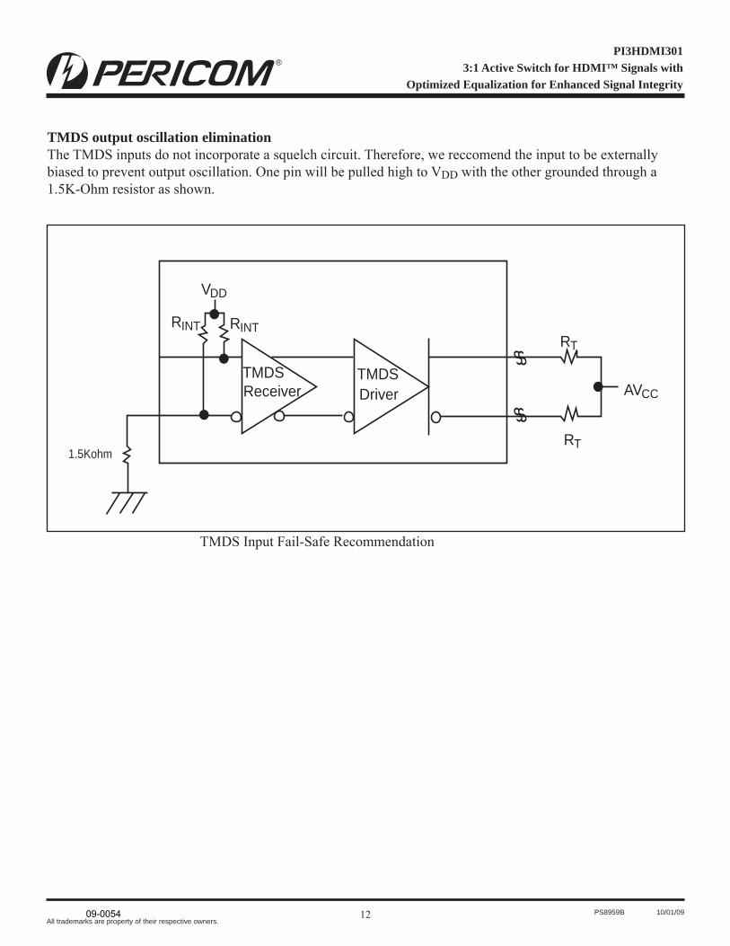
TMDS output oscillation eliminationThe TMDS inputs do not incorporate a squelch circuit. Therefore, we reccomend the input to be externally biased to prevent output oscillation. One pin will be pulled high to VDD with the other grounded through a 1.5K-Ohm resistor as shown.
TMDS Input Fail-Safe Recommendation
ss
ssRT
RT
AVCC
VDD
TMDS TMDSDriverReceiver
RINT RINT
1.5Kohm
09-0054

13 PS8959B 10/01/09
PI3HDMI3013:1 Active Switch for HDMI™ Signals with
Optimized Equalization for Enhanced Signal Integrity
ADVANCE INFORMATION - COMPANY CONFIDENTIAL
All trademarks are property of their respective owners.
Recommended Power Supply Decoupling CircuitFigure 1 is the recommended power supply decoupling circuit confi guration. It is recommended to put 0.1μF decoupling capacitors on each VDD pins of our part, there are four 0.1μF decoupling capacitors are put in Figure 1 with an assumption of only four VDD pins on our part, if there is more or less VDD pins on our Pericom parts, the number of 0.1μF decoupling capacitors should be adjust-ed according to the actual number of VDD pins. On top of 0.1μF decoupling capacitors on each VDD pins, it is recommended to put a 10μF decoupling capacitor near our part’s VDD, it is for stabilizing the power supply for our part. Ferrite bead is also recommended for isolating the power supply for our part and other power supplies in other parts of the circuit. But, it is optional and depends on the power supply conditions of other circuits.
Figure 1 Recommended Power Supply Decoupling Circuit Diagram
P e ric om P a rt
V DD
V DD
V DD
V DD
From main power supply
0.1μF
0.1μF
0.1μF
0.1μF
Ferrite Bead10μF
09-0054
14 PS8959B 10/01/09
PI3HDMI3013:1 Active Switch for HDMI™ Signals with
Optimized Equalization for Enhanced Signal Integrity
ADVANCE INFORMATION - COMPANY CONFIDENTIAL
All trademarks are property of their respective owners.
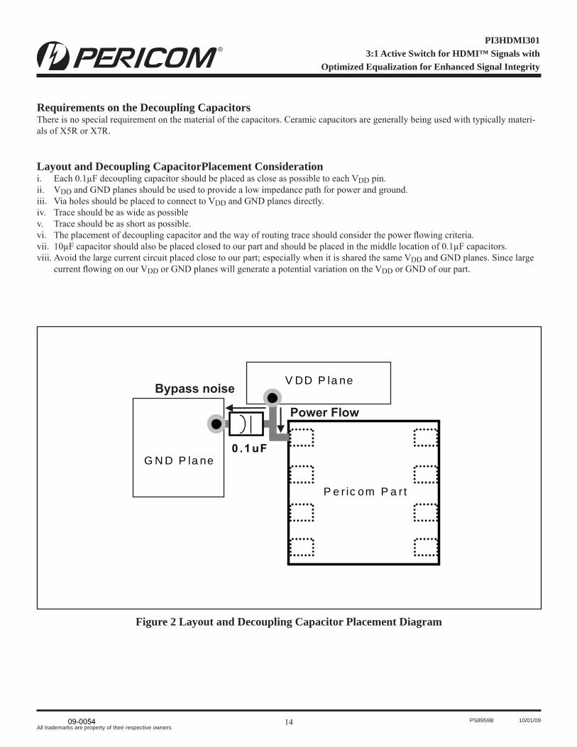
Requirements on the Decoupling CapacitorsThere is no special requirement on the material of the capacitors. Ceramic capacitors are generally being used with typically materi-als of X5R or X7R.
Layout and Decoupling CapacitorPlacement Considerationi. Each 0.1μF decoupling capacitor should be placed as close as possible to each VDD pin. ii. VDD and GND planes should be used to provide a low impedance path for power and ground.iii. Via holes should be placed to connect to VDD and GND planes directly.iv. Trace should be as wide as possiblev. Trace should be as short as possible. vi. The placement of decoupling capacitor and the way of routing trace should consider the power fl owing criteria.vii. 10μF capacitor should also be placed closed to our part and should be placed in the middle location of 0.1μF capacitors.viii. Avoid the large current circuit placed close to our part; especially when it is shared the same VDD and GND planes. Since large
current fl owing on our VDD or GND planes will generate a potential variation on the VDD or GND of our part.
Figure 2 Layout and Decoupling Capacitor Placement Diagram
P e r ic om P a r t
G N D P la ne
V DD P la ne
0 .1 uF
Bypass noise
Power Flow
09-0054
15 PS8959B 10/01/09
PI3HDMI3013:1 Active Switch for HDMI™ Signals with
Optimized Equalization for Enhanced Signal Integrity
ADVANCE INFORMATION - COMPANY CONFIDENTIAL
All trademarks are property of their respective owners.
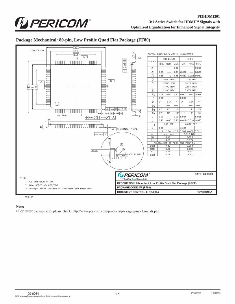
Package Mechanical: 80-pin, Low Profi le Quad Flat Package (FF80)
DESCRIPTION: 80-contact, Low Profi le Quad Flat Package (LQFP)PACKAGE CODE: FF (FF80)
DOCUMENT CONTROL #: PD-2064 REVISION: A
DATE: 03/18/09
07-0100
Top View:
Note:• For latest package info, please check: http://www.pericom.com/products/packaging/mechanicals.php
09-0054

16 PS8959B 10/01/09
PI3HDMI3013:1 Active Switch for HDMI™ Signals with
Optimized Equalization for Enhanced Signal Integrity
ADVANCE INFORMATION - COMPANY CONFIDENTIAL
All trademarks are property of their respective owners.
Pericom Semiconductor Corporation • 1-800-435-2336 • www.pericom.com
Ordering InformationOrdering Code Package Code Package DescriptionPI3HDMI301FFE FF 80-pin, Pb-free & Green LQFPPI3HDMI301ZLE ZL 64-pin, Pb-free & Green TQFN
Notes: • Thermal characteristics can be found on the company web site at www.pericom.com/packaging/
• E = Pb-free and Green • Adding an X Suffi x = Tape/Reel
Package Mechanical: 64-pin, Quad Flat Package (ZL64)
N F Q T , d a e L - o N t a l F d a u Q h c t i P e n i F n i h T , t c a t n o c - 4 6 : N O I T P I R C S E D L Z : E D O C E G A K C A P
7 6 0 2 - D P : # L O R T N O C T N E M U C O D B : N O I S I V E R
10/28/08: E T A D
08-0530
Top View: Bottom View:
Note:• For latest package info, please check: http://www.pericom.com/products/packaging/mechanicals.php
09-0054