Embed Size (px)
Citation preview
Thin Solid Films 556 (2014) 74–80
Contents lists available at ScienceDirect
Thin Solid Films
j ourna l homepage: www.e lsev ie r .com/ locate / ts f
Nucleation and crystallization of Li2O–Nb2O5 ternary compound thinfilms co-sputtered from LiNbO3 and Li2O targets
Housei AkazawaNTT Microsystem Integration Laboratories, 3-1 Morinosato Wakamiya, Atsugi, Kanagawa 243-0198, Japan
E-mail address: [email protected].
0040-6090/$ – see front matter © 2014 Elsevier B.V. All rihttp://dx.doi.org/10.1016/j.tsf.2014.01.013
a b s t r a c t
a r t i c l e i n f oArticle history:Received 24 March 2013Received in revised form 6 January 2014Accepted 6 January 2014Available online 15 January 2014
Keywords:NucleationCrystallizationLithium NiobateLithium OxideNiobium pentoxideSolid Phase EpitaxySputtering
Li2O–Nb2O5 ternary compound thin films were deposited by dual sputtering from LiNbO3 and Li2O targets tocover a wide range of Li/Nbmolar ratios. When all parts of the films were crystallized during sputtering at elevatedtemperatures, pyrochlore phase crystallites of Li3NbO4, LiNbO3, and LiNb3O8 were preferentially oriented towardtheir respective (222), (006), and (602) directions. These closely packed crystallographic planes having thelowest surface free energies were initially created under exposure to the plasma and the crystallization that follow-ed proceeded exclusively on these seed planes. The volume fraction of each crystalline component as a function ofthe Li/Nbmolar ratio obeyed the established phase diagram. In contrast, solid-phase crystallization of pre-depositedamorphous films through post annealing exhibited a non-equilibrium nature, and the volume fraction of each crys-talline component depended on the crystallization rate rather than the Li/Nbmolar ratio. Solid-phase crystallizationdecelerated when excess Li2O was contained in the film. Specifically, LiNbO3 crystallites with near-stoichiometriccompositions were randomly oriented without the operating mechanism of preferential orientation towardc-planes. In certain situations, crystalline domains were spatially of inhomogeneous composition, resultingin the simultaneous coexistence of Li3NbO4, LiNbO3, and LiNb3O8.
© 2014 Elsevier B.V. All rights reserved.
1. Introduction
LiNbO3 single crystal is a representative opto-electronic material [1]and its bulk crystal growth has long been studied [2–6]. LiNbO3 crystalsare endowed with various functional properties such as having ferro-electric, pyloelectric, electro-optic, and nonlinear optical effects [7].The electro-optic effect is the operating principle for high-frequencymodulators, fast optical switches, and Pockels sensors [8]. The nonlinearoptical effect is responsible for frequency-doubled lasers and wave-length converters [9–11]. The feasibility of the pyroelectric effect [12]has been demonstrated for compact X-ray sources [13]. Except forthese stand-alone devices, promising applications of LiNbO3 crystalscan be developed for integrated systems [14,15], for instance, in combi-nation with silicon photonics [16]. If a LiNbO3 layer is overlaid on a SiO2
layer, the sharp refractive index profile between the core (LiNbO3) andcladding (SiO2) layers enables propagating light to be efficiently con-fined within the LiNbO3 waveguide [17–22]. We can thus impart activefunctions to the optical circuit by placing LiNbO3 segments in the mid-section of silicon-based passive waveguides, which are typically madeof SiOx, SiON, and Si3N4 [23].
Featuring single crystals ensures basically the sameelectro-optic andfrequency conversion coefficient of the LiNbO3 crystal. To make hybridsystems, however, wafer bonding [24,25] and thinning processes incur
ghts reserved.
a great deal of cost. The product is a single optical component. In con-trast, depositing LiNbO3 film is a convenient approach for insertingLiNbO3 segments in advantageous places. It is compatible with pat-terned substrate and multiple layers can be formed if necessary. Theproblems accompanied with employing LiNbO3 polycrystalline filmsare their inferior properties compared with those of single crystalsdue to defects. In our previous attempts by using electron cyclotron res-onance (ECR) plasma sputteringwith a single LiNbO3 target [26], the O2
flow rate for a single phasewith amolar ratio of Li:Nb=3:1 to nucleatewas between 0.5 and 1 sccm. However, films grown under such a lowO2 flow rate were slightly oxygen-deficient LiNbO3−x. If the O2 flowrate was higher than 1 sccm, Li atoms, in contrast, reacted with oxygenradicals that were generated in the plasma, and the volatile Li2O mole-cules desorbed into the vacuum at high temperatures. This led to theformation of Li1−xNbO3 films. Although the standard approach forgrowing films with a molar ratio of Li:Nb:O = 1:1:3 is employing Li-excess targets, it is difficult to predict the exact target compositionthat will result in a stoichiometric composition.Moreover, the composi-tion of deposited filmsmay vary depending on the growth temperature,deposition rate, and other plasma parameters [27–30]. It is not guaran-teed that a stoichiometric compositionwill be obtainedwithin a param-eter range by only adjusting the O2 flow rate. Notwithstanding thisbackground, the composition should preferably be variable to meetdiverse demands in the actual process. Depending on the applicationfor the device, the factors affecting priority may be crystallinity, the do-main structure, surface roughness, or the deposition rate rather thanstoichiometry.
75H. Akazawa / Thin Solid Films 556 (2014) 74–80
In the work reported in this paper, we found adaptive control of thefilm composition to be close to that of the stoichiometric one. Prior toapproaching this goal, we studied the manner in which phases wereformed in the Li2O–Nb2O5 ternary compound system over a widerange of Li/Nb molar ratios. We employed dual sputtering from aLiNbO3 main target and a Li2O sub-target to tailor the film composition.Li and O atoms sputtered from the Li2O target supplemented Li atomsthat were lost in the form of Li2O from the film and from the LiNbO3 tar-get surface due to the impact with argon ions. We could vary the Li/Nbmolar ratio (x) in deposited films between 0.4 and 2, while maintainingsufficiently oxidized conditions.
The crystal growth sequence is composed of two steps, i.e., initiallyassembling atoms to create crystalline seeds (nucleation) and followingthis with growth on the seed crystal surfaces (crystallization) [31]. Bulkcrystal growth frommelts proceeds by extending the front of seed crys-tal at the liquid/solid interface. The nucleation step is skipped if a seedcrystal is provided. In contrast, crystal growth by molecular-beam epi-taxy, chemical vapor deposition, and sputtering proceeds at the vacu-um/solid interface. If an epitaxial substrate is not used, the initialnucleation process may govern the following crystallization step.Solid-phase crystallization is another route forming crystalline thinfilms, where nucleation begins not only at the solid–solid interface butalso at the surface and inside thefilmunder non-equilibriumconditions.The crystallization step will be greatly affected by the location wherenucleation occurs. Against this background, we tried to characterizethe crystal growth process during deposition (as-crystallization) aswell as the solid-phase crystallization of pre-deposited amorphousfilms (post-crystallization). In the latter case, we found that the migra-tion activity of constituent atoms was the primary parameter affectingphase formation and crystallization.
2. Experimental details
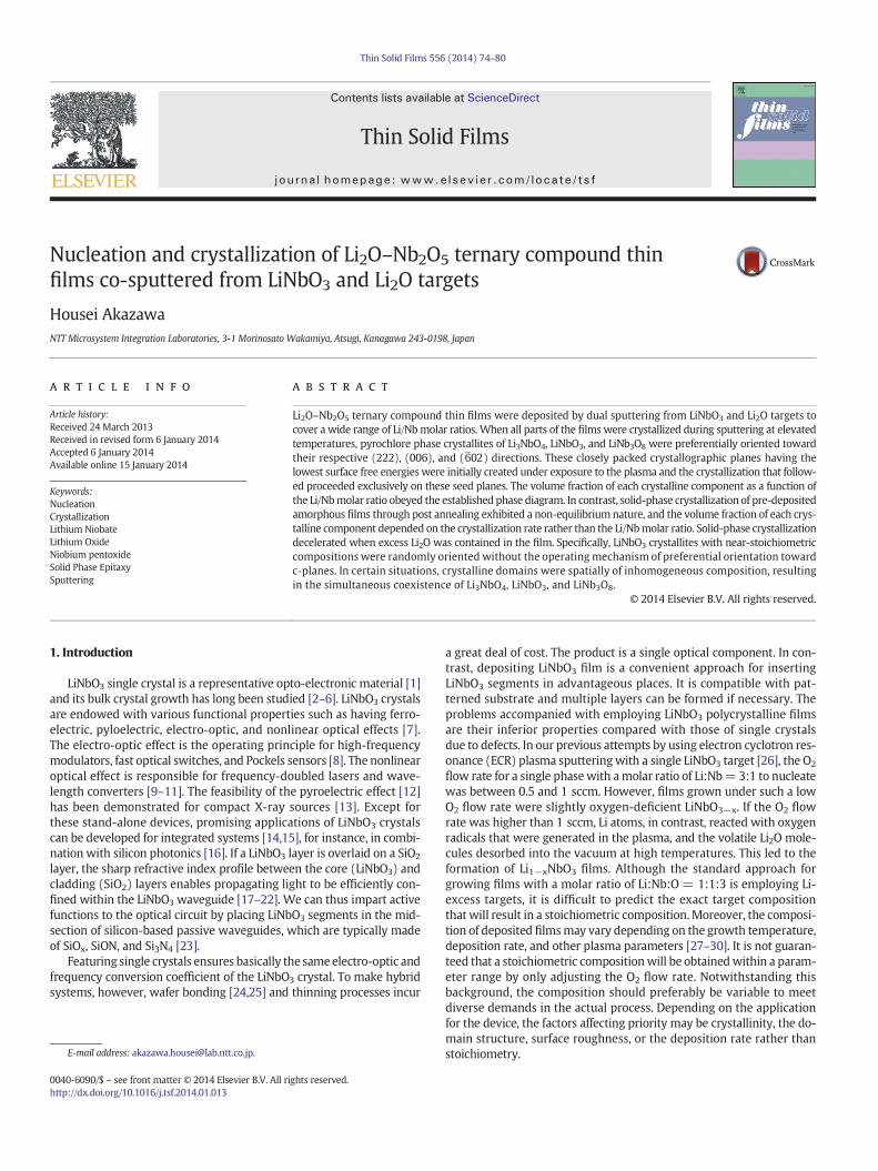
The geometrical configuration for our dual target sputtering systemis in Fig. 1. It is based on an ECR plasma sputtering system combinedwith an RF magnetron gun. In the ECR plasma source, transmitting mi-crowaves (500 W) through double facing windows generated remoteplasma from Ar/O2 gas mixtures when an external magnetic field wasapplied. We fixed the Ar flow rate at 8 sccm and the O2 flow rate at3 sccm. Li, Nb, and O atoms were sputtered by applying RF voltage(500 W) to the cylindrical LiNbO3 target. Deposition from the LiNbO3
target alone at this O2 flow rate formed Li1−xNbO3 films. Hence, we sup-plied Li and O atoms from the RF magnetron gun that was equippedwith a Li2O target under an operating power between 0 and 100 W.
Fig. 1. Geometrical configuration for ECR sputtering and RF magnetron sputtering.
The substrate surface was tilted at 30° from the direction of the ECRplasma source and 50° from the RF magnetron gun.
We used four-inch Si(100) wafers as substrates. Dipping them in a2.5% HF solution removed the native oxide layer and prepared ahydrogen-terminated surface. The reason why non-epitaxial Si sub-strates were used was to investigate the manner of phase formationthat was not guided by a crystalline template [26]. Deposition wasdone either at a substrate temperature of 510 °C or 70 °C. Irradiatingthe substrate surface with a plasma stream while the substrate wasnon-annealed with a heater raised the surface temperature up to70 °C. At 510 °C, crystalline films were produced in their depositedstate. Solid-phase crystallization of amorphous films that had been de-posited at 70 °C was driven by 3 h of post annealing at 600 °C in a vac-uum. Film thickness was measured by single-wavelength ellipsometryat a wavelength of 633 nm assuming that the extinction coefficientwas negligibly small. The values we obtained were confirmed to agreewith the differential thickness between bare (deposited) and masked(non-deposited) regions on a substrate surface, which was measuredwith a stylus step profiler. Although the Li/Nb molar ratio in lithium ni-obate films can be monitored by nondestructive optical measurementsuch as infrared absorption and Raman scattering spectroscopies[32–34], we employed inductively coupled plasma atomic emissionspectroscopy (ICP-AES) for quantitative evaluation.
The crystal structures were determined by X-ray diffraction (XRD)(RINT1500, Rigaku) by using a Cu Kα line as the primary X-raybeam. It is known that the Li2O–Nb2O5 ternary compound systemhas four stable compounds: 3Li2O·Nb2O5, Li2O·Nb2O5, Li2O·3Nb2O5,and Li2O·14Nb2O5 [35]. They correspond to the crystalline componentsof Li3NbO4, LiNbO3, LiNb3O8, and Li2Nb28O71. Of these, Li2Nb28O71
appearing at extremely Li deficient compositions was beyond therange of compositions that could be prepared in our deposition system.The other three components, if they were selectively orientated,could clearly be distinguished in terms of the primary XRD signalsof Li3NbO4(222), LiNbO3(006), and LiNb3O8(602), which appearat respective 2θ angles of 37°, 39°, and 38°.
3. Results
3.1. Distribution of thickness and composition over 4-inch substrate surface
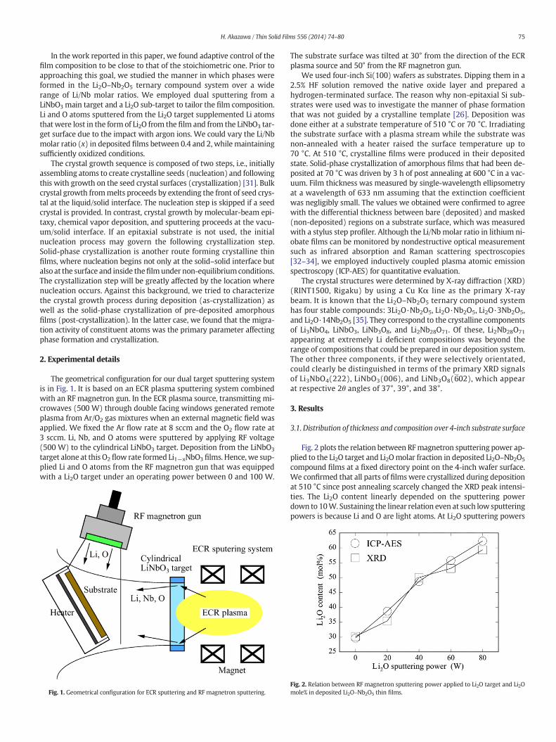
Fig. 2 plots the relation between RFmagnetron sputtering power ap-plied to the Li2O target and Li2Omolar fraction in deposited Li2O–Nb2O5
compound films at a fixed directory point on the 4-inch wafer surface.We confirmed that all parts of filmswere crystallized during depositionat 510 °C since post annealing scarcely changed the XRD peak intensi-ties. The Li2O content linearly depended on the sputtering powerdown to 10W. Sustaining the linear relation even at such low sputteringpowers is because Li and O are light atoms. At Li2O sputtering powers
Fig. 2. Relation between RF magnetron sputtering power applied to Li2O target and Li2Omole% in deposited Li2O–Nb2O5 thin films.
76 H. Akazawa / Thin Solid Films 556 (2014) 74–80
lower than 20 W, only LiNbO3(006) and LiNb3O8(602) peaks emergedand the Li2O content could be estimated from the integrated intensitiesof these peaks. In our previous paper analyzing LiNbO3 − x films depos-ited from a LiNbO3 target alone [26], we confirmed that the peak inten-sities of LiNbO3(006) and LiNb3O8( 602 ) scale with the Li/Nbconcentration ratio are derived from ICP-AES. Fig. 2 reveals that compo-sitions evaluated from XRD almost agreed with those derived from ICP-AES within an accuracy of ±8%. If compared for the same Li2Osputtering power, we could not find difference between the Li/Nbratio of amorphous Li2O–Nb2O5 compound films and that of films crys-tallized at 510 °C during sputtering.
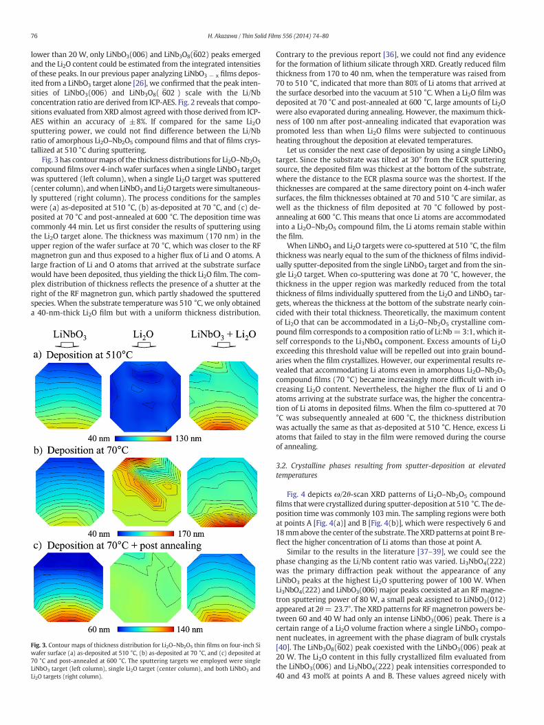
Fig. 3 has contourmaps of the thickness distributions for Li2O–Nb2O5
compound films over 4-inchwafer surfaces when a single LiNbO3 targetwas sputtered (left column), when a single Li2O target was sputtered(center column), andwhen LiNbO3 and Li2O targetswere simultaneous-ly sputtered (right column). The process conditions for the sampleswere (a) as-deposited at 510 °C, (b) as-deposited at 70 °C, and (c) de-posited at 70 °C and post-annealed at 600 °C. The deposition time wascommonly 44 min. Let us first consider the results of sputtering usingthe Li2O target alone. The thickness was maximum (170 nm) in theupper region of the wafer surface at 70 °C, which was closer to the RFmagnetron gun and thus exposed to a higher flux of Li and O atoms. Alarge fraction of Li and O atoms that arrived at the substrate surfacewould have been deposited, thus yielding the thick Li2O film. The com-plex distribution of thickness reflects the presence of a shutter at theright of the RF magnetron gun, which partly shadowed the sputteredspecies. When the substrate temperature was 510 °C, we only obtaineda 40-nm-thick Li2O film but with a uniform thickness distribution.
Fig. 3. Contour maps of thickness distribution for Li2O–Nb2O5 thin films on four-inch Siwafer surface (a) as-deposited at 510 °C, (b) as-deposited at 70 °C, and (c) deposited at70 °C and post-annealed at 600 °C. The sputtering targets we employed were singleLiNbO3 target (left column), single Li2O target (center column), and both LiNbO3 andLi2O targets (right column).
Contrary to the previous report [36], we could not find any evidencefor the formation of lithium silicate through XRD. Greatly reduced filmthickness from 170 to 40 nm, when the temperature was raised from70 to 510 °C, indicated that more than 80% of Li atoms that arrived atthe surface desorbed into the vacuum at 510 °C. When a Li2O film wasdeposited at 70 °C and post-annealed at 600 °C, large amounts of Li2Owere also evaporated during annealing. However, the maximum thick-ness of 100 nm after post-annealing indicated that evaporation waspromoted less than when Li2O films were subjected to continuousheating throughout the deposition at elevated temperatures.
Let us consider the next case of deposition by using a single LiNbO3
target. Since the substrate was tilted at 30° from the ECR sputteringsource, the deposited film was thickest at the bottom of the substrate,where the distance to the ECR plasma source was the shortest. If thethicknesses are compared at the same directory point on 4-inch wafersurfaces, the film thicknesses obtained at 70 and 510 °C are similar, aswell as the thickness of film deposited at 70 °C followed by post-annealing at 600 °C. This means that once Li atoms are accommodatedinto a Li2O–Nb2O5 compound film, the Li atoms remain stable withinthe film.
When LiNbO3 and Li2O targets were co-sputtered at 510 °C, the filmthickness was nearly equal to the sum of the thickness of films individ-ually sputter-deposited from the single LiNbO3 target and from the sin-gle Li2O target. When co-sputtering was done at 70 °C, however, thethickness in the upper region was markedly reduced from the totalthickness of films individually sputtered from the Li2O and LiNbO3 tar-gets, whereas the thickness at the bottom of the substrate nearly coin-cided with their total thickness. Theoretically, the maximum contentof Li2O that can be accommodated in a Li2O–Nb2O5 crystalline com-pound film corresponds to a composition ratio of Li:Nb= 3:1, which it-self corresponds to the Li3NbO4 component. Excess amounts of Li2Oexceeding this threshold value will be repelled out into grain bound-aries when the film crystallizes. However, our experimental results re-vealed that accommodating Li atoms even in amorphous Li2O–Nb2O5
compound films (70 °C) became increasingly more difficult with in-creasing Li2O content. Nevertheless, the higher the flux of Li and Oatoms arriving at the substrate surface was, the higher the concentra-tion of Li atoms in deposited films. When the film co-sputtered at 70°C was subsequently annealed at 600 °C, the thickness distributionwas actually the same as that as-deposited at 510 °C. Hence, excess Liatoms that failed to stay in the film were removed during the courseof annealing.
3.2. Crystalline phases resulting from sputter-deposition at elevatedtemperatures
Fig. 4 depicts ω/2θ-scan XRD patterns of Li2O–Nb2O5 compoundfilms thatwere crystallized during sputter-deposition at 510 °C. The de-position timewas commonly 103min. The sampling regions were bothat points A [Fig. 4(a)] and B [Fig. 4(b)], which were respectively 6 and18mmabove the center of the substrate. TheXRDpatterns at point B re-flect the higher concentration of Li atoms than those at point A.
Similar to the results in the literature [37–39], we could see thephase changing as the Li/Nb content ratio was varied. Li3NbO4(222)was the primary diffraction peak without the appearance of anyLiNbO3 peaks at the highest Li2O sputtering power of 100 W. WhenLi3NbO4(222) and LiNbO3(006) major peaks coexisted at an RF magne-tron sputtering power of 80 W, a small peak assigned to LiNbO3(012)appeared at 2θ= 23.7°. The XRD patterns for RFmagnetron powers be-tween 60 and 40 W had only an intense LiNbO3(006) peak. There is acertain range of a Li2O volume fraction where a single LiNbO3 compo-nent nucleates, in agreement with the phase diagram of bulk crystals[40]. The LiNb3O8(602) peak coexisted with the LiNbO3(006) peak at20 W. The Li2O content in this fully crystallized film evaluated fromthe LiNbO3(006) and Li3NbO4(222) peak intensities corresponded to40 and 43 mol% at points A and B. These values agreed nicely with
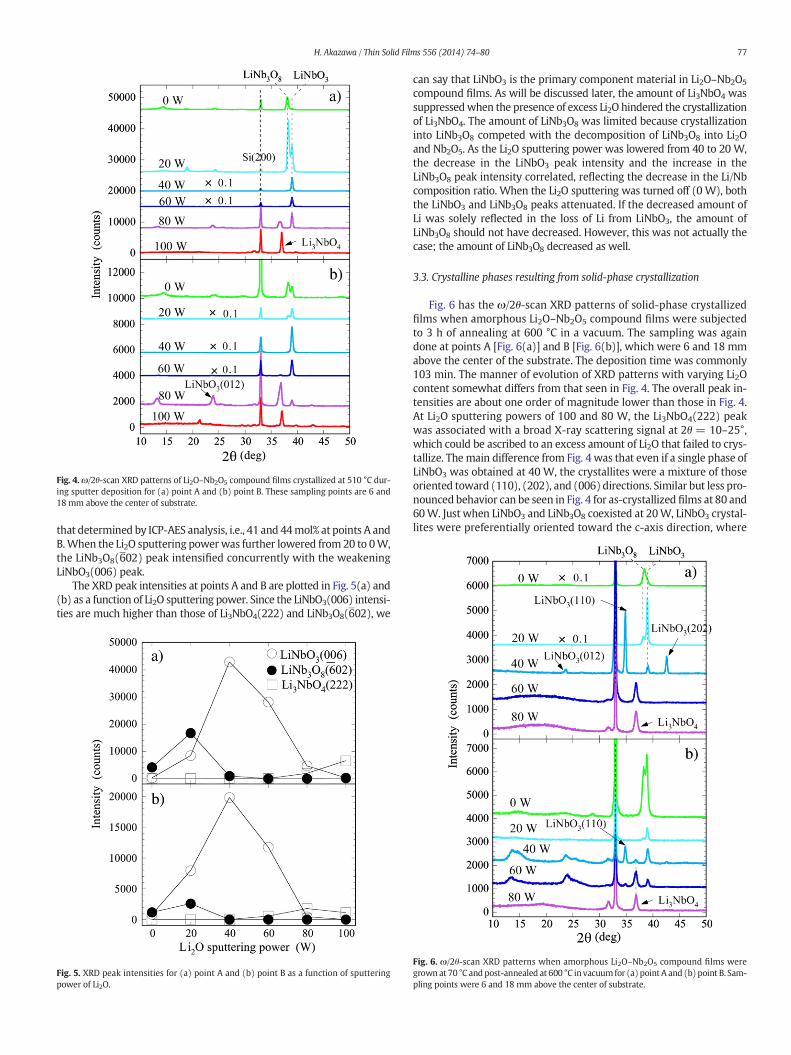
Fig. 4.ω/2θ-scan XRD patterns of Li2O–Nb2O5 compound films crystallized at 510 °C dur-ing sputter deposition for (a) point A and (b) point B. These sampling points are 6 and18 mm above the center of substrate.
77H. Akazawa / Thin Solid Films 556 (2014) 74–80
that determined by ICP-AES analysis, i.e., 41 and 44mol% at points A andB.When the Li2O sputtering powerwas further lowered from 20 to 0W,the LiNb3O8(602) peak intensified concurrently with the weakeningLiNbO3(006) peak.
The XRD peak intensities at points A and B are plotted in Fig. 5(a) and(b) as a function of Li2O sputtering power. Since the LiNbO3(006) intensi-ties are much higher than those of Li3NbO4(222) and LiNb3O8(602), we
Fig. 5. XRD peak intensities for (a) point A and (b) point B as a function of sputteringpower of Li2O.
can say that LiNbO3 is the primary component material in Li2O–Nb2O5
compound films. As will be discussed later, the amount of Li3NbO4 wassuppressedwhen the presence of excess Li2O hindered the crystallizationof Li3NbO4. The amount of LiNb3O8 was limited because crystallizationinto LiNb3O8 competed with the decomposition of LiNb3O8 into Li2Oand Nb2O5. As the Li2O sputtering power was lowered from 40 to 20 W,the decrease in the LiNbO3 peak intensity and the increase in theLiNb3O8 peak intensity correlated, reflecting the decrease in the Li/Nbcomposition ratio. When the Li2O sputtering was turned off (0 W), boththe LiNbO3 and LiNb3O8 peaks attenuated. If the decreased amount ofLi was solely reflected in the loss of Li from LiNbO3, the amount ofLiNb3O8 should not have decreased. However, this was not actually thecase; the amount of LiNb3O8 decreased as well.
3.3. Crystalline phases resulting from solid-phase crystallization
Fig. 6 has the ω/2θ-scan XRD patterns of solid-phase crystallizedfilms when amorphous Li2O–Nb2O5 compound films were subjectedto 3 h of annealing at 600 °C in a vacuum. The sampling was againdone at points A [Fig. 6(a)] and B [Fig. 6(b)], which were 6 and 18 mmabove the center of the substrate. The deposition time was commonly103 min. The manner of evolution of XRD patterns with varying Li2Ocontent somewhat differs from that seen in Fig. 4. The overall peak in-tensities are about one order of magnitude lower than those in Fig. 4.At Li2O sputtering powers of 100 and 80 W, the Li3NbO4(222) peakwas associated with a broad X-ray scattering signal at 2θ = 10–25°,which could be ascribed to an excess amount of Li2O that failed to crys-tallize. The main difference from Fig. 4 was that even if a single phase ofLiNbO3 was obtained at 40 W, the crystallites were a mixture of thoseoriented toward (110), (202), and (006) directions. Similar but less pro-nounced behavior can be seen in Fig. 4 for as-crystallized films at 80 and60W. Just when LiNbO3 and LiNb3O8 coexisted at 20W, LiNbO3 crystal-lites were preferentially oriented toward the c-axis direction, where
Fig. 6. ω/2θ-scan XRD patterns when amorphous Li2O–Nb2O5 compound films weregrown at 70 °C andpost-annealed at 600 °C invacuum for (a) point A and (b) point B. Sam-pling points were 6 and 18 mm above the center of substrate.
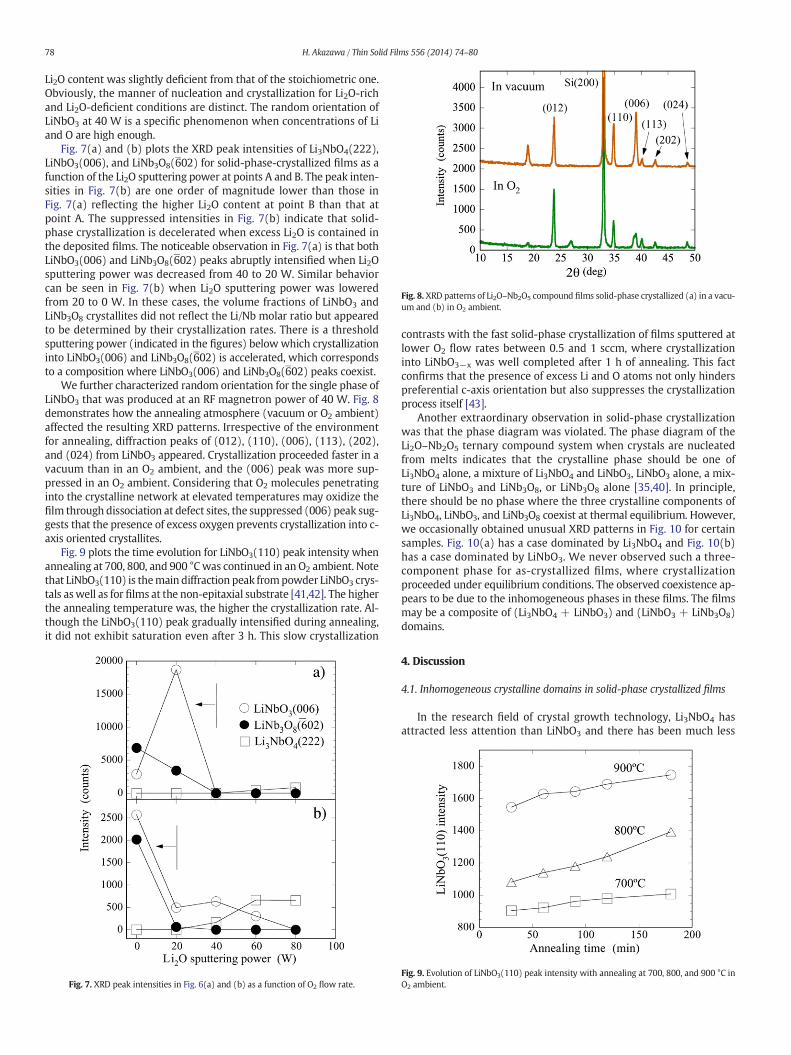
Fig. 8. XRD patterns of Li2O–Nb2O5 compound films solid-phase crystallized (a) in a vacu-um and (b) in O2 ambient.
78 H. Akazawa / Thin Solid Films 556 (2014) 74–80
Li2O content was slightly deficient from that of the stoichiometric one.Obviously, the manner of nucleation and crystallization for Li2O-richand Li2O-deficient conditions are distinct. The random orientation ofLiNbO3 at 40 W is a specific phenomenon when concentrations of Liand O are high enough.
Fig. 7(a) and (b) plots the XRD peak intensities of Li3NbO4(222),LiNbO3(006), and LiNb3O8(602) for solid-phase-crystallized films as afunction of the Li2O sputtering power at points A and B. The peak inten-sities in Fig. 7(b) are one order of magnitude lower than those inFig. 7(a) reflecting the higher Li2O content at point B than that atpoint A. The suppressed intensities in Fig. 7(b) indicate that solid-phase crystallization is decelerated when excess Li2O is contained inthe deposited films. The noticeable observation in Fig. 7(a) is that bothLiNbO3(006) and LiNb3O8(602) peaks abruptly intensified when Li2Osputtering power was decreased from 40 to 20 W. Similar behaviorcan be seen in Fig. 7(b) when Li2O sputtering power was loweredfrom 20 to 0 W. In these cases, the volume fractions of LiNbO3 andLiNb3O8 crystallites did not reflect the Li/Nb molar ratio but appearedto be determined by their crystallization rates. There is a thresholdsputtering power (indicated in the figures) below which crystallizationinto LiNbO3(006) and LiNb3O8(602) is accelerated, which correspondsto a composition where LiNbO3(006) and LiNb3O8(602) peaks coexist.
We further characterized random orientation for the single phase ofLiNbO3 that was produced at an RF magnetron power of 40 W. Fig. 8demonstrates how the annealing atmosphere (vacuum or O2 ambient)affected the resulting XRD patterns. Irrespective of the environmentfor annealing, diffraction peaks of (012), (110), (006), (113), (202),and (024) from LiNbO3 appeared. Crystallization proceeded faster in avacuum than in an O2 ambient, and the (006) peak was more sup-pressed in an O2 ambient. Considering that O2 molecules penetratinginto the crystalline network at elevated temperatures may oxidize thefilm through dissociation at defect sites, the suppressed (006) peak sug-gests that the presence of excess oxygen prevents crystallization into c-axis oriented crystallites.
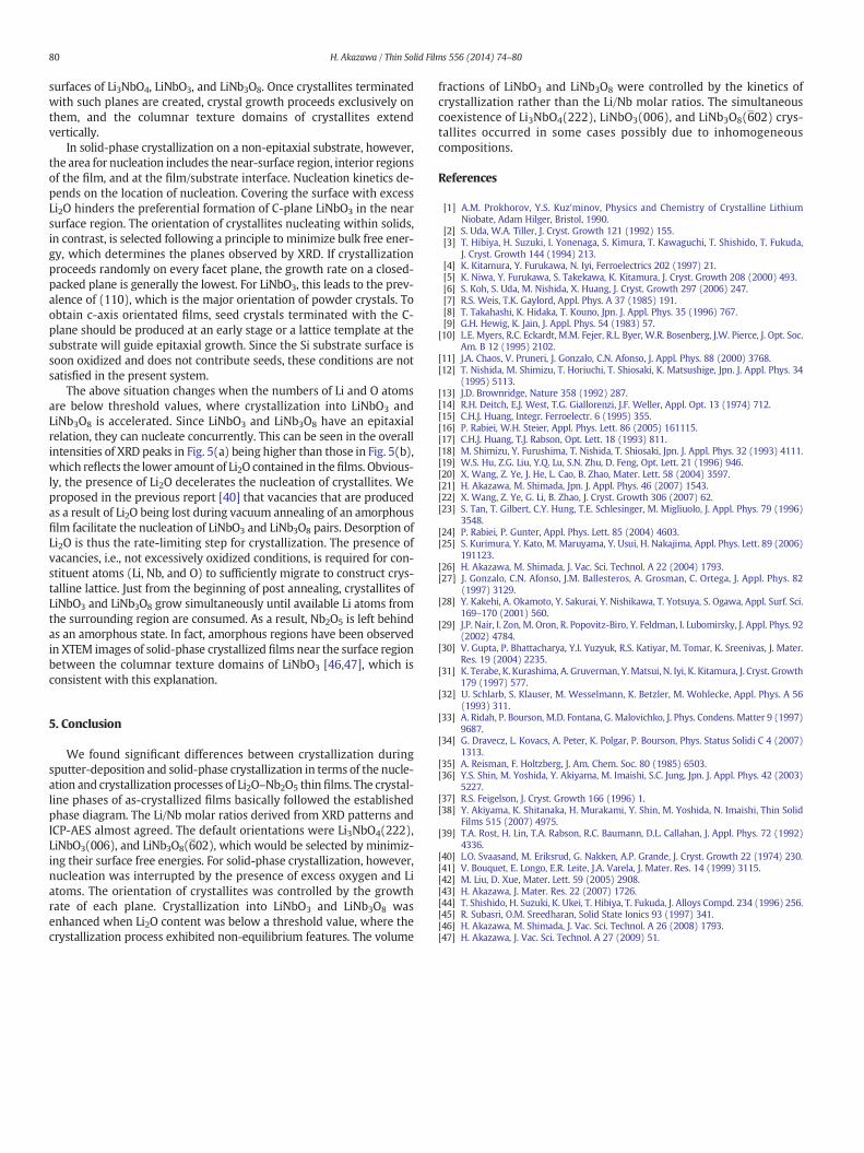
Fig. 9 plots the time evolution for LiNbO3(110) peak intensity whenannealing at 700, 800, and 900 °C was continued in an O2 ambient. Notethat LiNbO3(110) is themain diffraction peak frompowder LiNbO3 crys-tals aswell as for films at the non-epitaxial substrate [41,42]. The higherthe annealing temperature was, the higher the crystallization rate. Al-though the LiNbO3(110) peak gradually intensified during annealing,it did not exhibit saturation even after 3 h. This slow crystallization
Fig. 7. XRD peak intensities in Fig. 6(a) and (b) as a function of O2 flow rate.
contrasts with the fast solid-phase crystallization of films sputtered atlower O2 flow rates between 0.5 and 1 sccm, where crystallizationinto LiNbO3−x was well completed after 1 h of annealing. This factconfirms that the presence of excess Li and O atoms not only hinderspreferential c-axis orientation but also suppresses the crystallizationprocess itself [43].
Another extraordinary observation in solid-phase crystallizationwas that the phase diagram was violated. The phase diagram of theLi2O–Nb2O5 ternary compound system when crystals are nucleatedfrom melts indicates that the crystalline phase should be one ofLi3NbO4 alone, a mixture of Li3NbO4 and LiNbO3, LiNbO3 alone, a mix-ture of LiNbO3 and LiNb3O8, or LiNb3O8 alone [35,40]. In principle,there should be no phase where the three crystalline components ofLi3NbO4, LiNbO3, and LiNb3O8 coexist at thermal equilibrium. However,we occasionally obtained unusual XRD patterns in Fig. 10 for certainsamples. Fig. 10(a) has a case dominated by Li3NbO4 and Fig. 10(b)has a case dominated by LiNbO3. We never observed such a three-component phase for as-crystallized films, where crystallizationproceeded under equilibrium conditions. The observed coexistence ap-pears to be due to the inhomogeneous phases in these films. The filmsmay be a composite of (Li3NbO4 + LiNbO3) and (LiNbO3 + LiNb3O8)domains.
4. Discussion
4.1. Inhomogeneous crystalline domains in solid-phase crystallized films
In the research field of crystal growth technology, Li3NbO4 hasattracted less attention than LiNbO3 and there has been much less
Fig. 9. Evolution of LiNbO3(110) peak intensity with annealing at 700, 800, and 900 °C inO2 ambient.
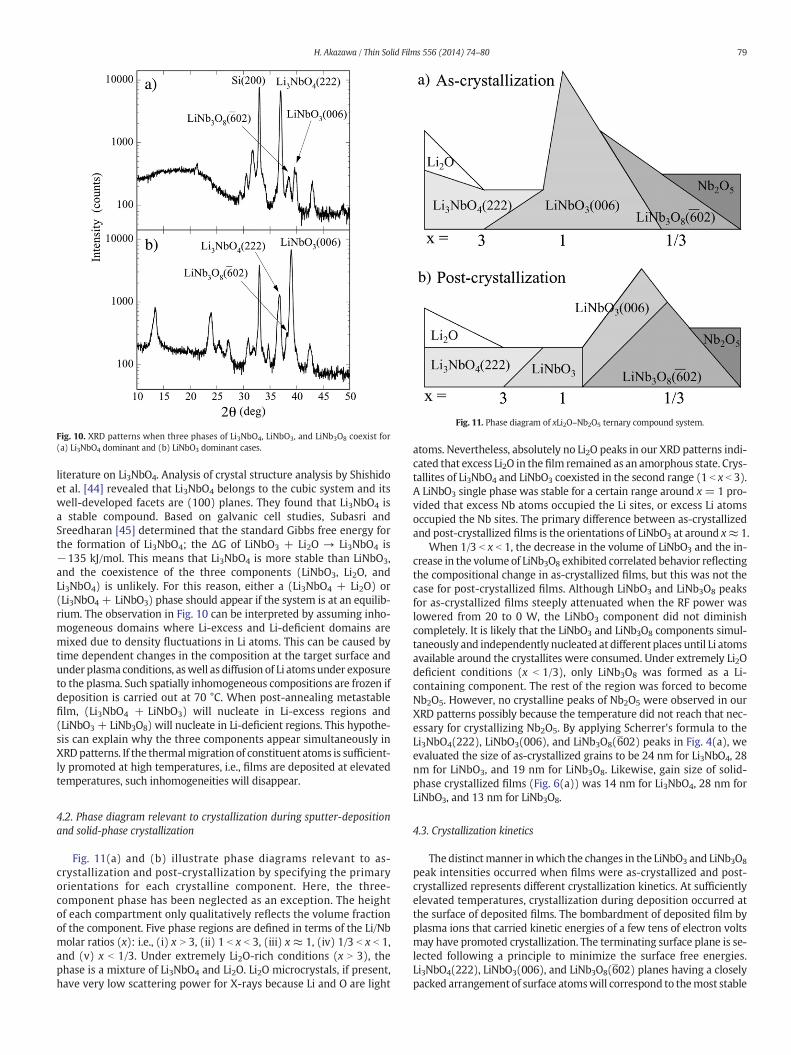
Fig. 10. XRD patterns when three phases of Li3NbO4, LiNbO3, and LiNb3O8 coexist for(a) Li3NbO4 dominant and (b) LiNbO3 dominant cases.
Fig. 11. Phase diagram of xLi2O–Nb2O5 ternary compound system.
79H. Akazawa / Thin Solid Films 556 (2014) 74–80
literature on Li3NbO4. Analysis of crystal structure analysis by Shishidoet al. [44] revealed that Li3NbO4 belongs to the cubic system and itswell-developed facets are (100) planes. They found that Li3NbO4 isa stable compound. Based on galvanic cell studies, Subasri andSreedharan [45] determined that the standard Gibbs free energy forthe formation of Li3NbO4; the ΔG of LiNbO3 + Li2O → Li3NbO4 is−135 kJ/mol. This means that Li3NbO4 is more stable than LiNbO3,and the coexistence of the three components (LiNbO3, Li2O, andLi3NbO4) is unlikely. For this reason, either a (Li3NbO4 + Li2O) or(Li3NbO4 + LiNbO3) phase should appear if the system is at an equilib-rium. The observation in Fig. 10 can be interpreted by assuming inho-mogeneous domains where Li-excess and Li-deficient domains aremixed due to density fluctuations in Li atoms. This can be caused bytime dependent changes in the composition at the target surface andunder plasma conditions, aswell as diffusion of Li atomsunder exposureto the plasma. Such spatially inhomogeneous compositions are frozen ifdeposition is carried out at 70 °C. When post-annealing metastablefilm, (Li3NbO4 + LiNbO3) will nucleate in Li-excess regions and(LiNbO3 + LiNb3O8) will nucleate in Li-deficient regions. This hypothe-sis can explain why the three components appear simultaneously inXRDpatterns. If the thermalmigration of constituent atoms is sufficient-ly promoted at high temperatures, i.e., films are deposited at elevatedtemperatures, such inhomogeneities will disappear.
4.2. Phase diagram relevant to crystallization during sputter-depositionand solid-phase crystallization
Fig. 11(a) and (b) illustrate phase diagrams relevant to as-crystallization and post-crystallization by specifying the primaryorientations for each crystalline component. Here, the three-component phase has been neglected as an exception. The heightof each compartment only qualitatively reflects the volume fractionof the component. Five phase regions are defined in terms of the Li/Nbmolar ratios (x): i.e., (i) x N 3, (ii) 1 b x b 3, (iii) x ≈ 1, (iv) 1/3 b x b 1,and (v) x b 1/3. Under extremely Li2O-rich conditions (x N 3), thephase is a mixture of Li3NbO4 and Li2O. Li2O microcrystals, if present,have very low scattering power for X-rays because Li and O are light
atoms. Nevertheless, absolutely no Li2O peaks in our XRD patterns indi-cated that excess Li2O in the film remained as an amorphous state. Crys-tallites of Li3NbO4 and LiNbO3 coexisted in the second range (1 b x b 3).A LiNbO3 single phase was stable for a certain range around x= 1 pro-vided that excess Nb atoms occupied the Li sites, or excess Li atomsoccupied the Nb sites. The primary difference between as-crystallizedand post-crystallized films is the orientations of LiNbO3 at around x≈ 1.
When 1/3 b x b 1, the decrease in the volume of LiNbO3 and the in-crease in the volume of LiNb3O8 exhibited correlated behavior reflectingthe compositional change in as-crystallized films, but this was not thecase for post-crystallized films. Although LiNbO3 and LiNb3O8 peaksfor as-crystallized films steeply attenuated when the RF power waslowered from 20 to 0 W, the LiNbO3 component did not diminishcompletely. It is likely that the LiNbO3 and LiNb3O8 components simul-taneously and independently nucleated at different places until Li atomsavailable around the crystallites were consumed. Under extremely Li2Odeficient conditions (x b 1/3), only LiNb3O8 was formed as a Li-containing component. The rest of the region was forced to becomeNb2O5. However, no crystalline peaks of Nb2O5 were observed in ourXRD patterns possibly because the temperature did not reach that nec-essary for crystallizing Nb2O5. By applying Scherrer's formula to theLi3NbO4(222), LiNbO3(006), and LiNb3O8(602) peaks in Fig. 4(a), weevaluated the size of as-crystallized grains to be 24 nm for Li3NbO4, 28nm for LiNbO3, and 19 nm for LiNb3O8. Likewise, gain size of solid-phase crystallized films (Fig. 6(a)) was 14 nm for Li3NbO4, 28 nm forLiNbO3, and 13 nm for LiNb3O8.
4.3. Crystallization kinetics
The distinctmanner inwhich the changes in the LiNbO3 and LiNb3O8
peak intensities occurred when films were as-crystallized and post-crystallized represents different crystallization kinetics. At sufficientlyelevated temperatures, crystallization during deposition occurred atthe surface of deposited films. The bombardment of deposited film byplasma ions that carried kinetic energies of a few tens of electron voltsmay have promoted crystallization. The terminating surface plane is se-lected following a principle to minimize the surface free energies.Li3NbO4(222), LiNbO3(006), and LiNb3O8(602) planes having a closelypacked arrangement of surface atomswill correspond to themost stable
80 H. Akazawa / Thin Solid Films 556 (2014) 74–80
surfaces of Li3NbO4, LiNbO3, and LiNb3O8. Once crystallites terminatedwith such planes are created, crystal growth proceeds exclusively onthem, and the columnar texture domains of crystallites extendvertically.
In solid-phase crystallization on a non-epitaxial substrate, however,the area for nucleation includes the near-surface region, interior regionsof the film, and at the film/substrate interface. Nucleation kinetics de-pends on the location of nucleation. Covering the surface with excessLi2O hinders the preferential formation of C-plane LiNbO3 in the nearsurface region. The orientation of crystallites nucleating within solids,in contrast, is selected following a principle to minimize bulk free ener-gy, which determines the planes observed by XRD. If crystallizationproceeds randomly on every facet plane, the growth rate on a closed-packed plane is generally the lowest. For LiNbO3, this leads to the prev-alence of (110), which is the major orientation of powder crystals. Toobtain c-axis orientated films, seed crystals terminated with the C-plane should be produced at an early stage or a lattice template at thesubstrate will guide epitaxial growth. Since the Si substrate surface issoon oxidized and does not contribute seeds, these conditions are notsatisfied in the present system.
The above situation changes when the numbers of Li and O atomsare below threshold values, where crystallization into LiNbO3 andLiNb3O8 is accelerated. Since LiNbO3 and LiNb3O8 have an epitaxialrelation, they can nucleate concurrently. This can be seen in the overallintensities of XRD peaks in Fig. 5(a) being higher than those in Fig. 5(b),which reflects the lower amount of Li2O contained in thefilms. Obvious-ly, the presence of Li2O decelerates the nucleation of crystallites. Weproposed in the previous report [40] that vacancies that are producedas a result of Li2O being lost during vacuum annealing of an amorphousfilm facilitate the nucleation of LiNbO3 and LiNb3O8 pairs. Desorption ofLi2O is thus the rate-limiting step for crystallization. The presence ofvacancies, i.e., not excessively oxidized conditions, is required for con-stituent atoms (Li, Nb, and O) to sufficiently migrate to construct crys-talline lattice. Just from the beginning of post annealing, crystallites ofLiNbO3 and LiNb3O8 grow simultaneously until available Li atoms fromthe surrounding region are consumed. As a result, Nb2O5 is left behindas an amorphous state. In fact, amorphous regions have been observedin XTEM images of solid-phase crystallized films near the surface regionbetween the columnar texture domains of LiNbO3 [46,47], which isconsistent with this explanation.
5. Conclusion
We found significant differences between crystallization duringsputter-deposition and solid-phase crystallization in terms of the nucle-ation and crystallization processes of Li2O–Nb2O5 thin films. The crystal-line phases of as-crystallized films basically followed the establishedphase diagram. The Li/Nb molar ratios derived from XRD patterns andICP-AES almost agreed. The default orientations were Li3NbO4(222),LiNbO3(006), and LiNb3O8(602), which would be selected by minimiz-ing their surface free energies. For solid-phase crystallization, however,nucleation was interrupted by the presence of excess oxygen and Liatoms. The orientation of crystallites was controlled by the growthrate of each plane. Crystallization into LiNbO3 and LiNb3O8 wasenhanced when Li2O content was below a threshold value, where thecrystallization process exhibited non-equilibrium features. The volume
fractions of LiNbO3 and LiNb3O8 were controlled by the kinetics ofcrystallization rather than the Li/Nb molar ratios. The simultaneouscoexistence of Li3NbO4(222), LiNbO3(006), and LiNb3O8(602) crys-tallites occurred in some cases possibly due to inhomogeneouscompositions.
References
[1] A.M. Prokhorov, Y.S. Kuz'minov, Physics and Chemistry of Crystalline LithiumNiobate, Adam Hilger, Bristol, 1990.
[2] S. Uda, W.A. Tiller, J. Cryst. Growth 121 (1992) 155.[3] T. Hibiya, H. Suzuki, I. Yonenaga, S. Kimura, T. Kawaguchi, T. Shishido, T. Fukuda,
J. Cryst. Growth 144 (1994) 213.[4] K. Kitamura, Y. Furukawa, N. Iyi, Ferroelectrics 202 (1997) 21.[5] K. Niwa, Y. Furukawa, S. Takekawa, K. Kitamura, J. Cryst. Growth 208 (2000) 493.[6] S. Koh, S. Uda, M. Nishida, X. Huang, J. Cryst. Growth 297 (2006) 247.[7] R.S. Weis, T.K. Gaylord, Appl. Phys. A 37 (1985) 191.[8] T. Takahashi, K. Hidaka, T. Kouno, Jpn. J. Appl. Phys. 35 (1996) 767.[9] G.H. Hewig, K. Jain, J. Appl. Phys. 54 (1983) 57.
[10] L.E. Myers, R.C. Eckardt, M.M. Fejer, R.L. Byer, W.R. Bosenberg, J.W. Pierce, J. Opt. Soc.Am. B 12 (1995) 2102.
[11] J.A. Chaos, V. Pruneri, J. Gonzalo, C.N. Afonso, J. Appl. Phys. 88 (2000) 3768.[12] T. Nishida, M. Shimizu, T. Horiuchi, T. Shiosaki, K. Matsushige, Jpn. J. Appl. Phys. 34
(1995) 5113.[13] J.D. Brownridge, Nature 358 (1992) 287.[14] R.H. Deitch, E.J. West, T.G. Giallorenzi, J.F. Weller, Appl. Opt. 13 (1974) 712.[15] C.H.J. Huang, Integr. Ferroelectr. 6 (1995) 355.[16] P. Rabiei, W.H. Steier, Appl. Phys. Lett. 86 (2005) 161115.[17] C.H.J. Huang, T.J. Rabson, Opt. Lett. 18 (1993) 811.[18] M. Shimizu, Y. Furushima, T. Nishida, T. Shiosaki, Jpn. J. Appl. Phys. 32 (1993) 4111.[19] W.S. Hu, Z.G. Liu, Y.Q. Lu, S.N. Zhu, D. Feng, Opt. Lett. 21 (1996) 946.[20] X. Wang, Z. Ye, J. He, L. Cao, B. Zhao, Mater. Lett. 58 (2004) 3597.[21] H. Akazawa, M. Shimada, Jpn. J. Appl. Phys. 46 (2007) 1543.[22] X. Wang, Z. Ye, G. Li, B. Zhao, J. Cryst. Growth 306 (2007) 62.[23] S. Tan, T. Gilbert, C.Y. Hung, T.E. Schlesinger, M. Migliuolo, J. Appl. Phys. 79 (1996)
3548.[24] P. Rabiei, P. Gunter, Appl. Phys. Lett. 85 (2004) 4603.[25] S. Kurimura, Y. Kato, M. Maruyama, Y. Usui, H. Nakajima, Appl. Phys. Lett. 89 (2006)
191123.[26] H. Akazawa, M. Shimada, J. Vac. Sci. Technol. A 22 (2004) 1793.[27] J. Gonzalo, C.N. Afonso, J.M. Ballesteros, A. Grosman, C. Ortega, J. Appl. Phys. 82
(1997) 3129.[28] Y. Kakehi, A. Okamoto, Y. Sakurai, Y. Nishikawa, T. Yotsuya, S. Ogawa, Appl. Surf. Sci.
169–170 (2001) 560.[29] J.P. Nair, I. Zon, M. Oron, R. Popovitz-Biro, Y. Feldman, I. Lubomirsky, J. Appl. Phys. 92
(2002) 4784.[30] V. Gupta, P. Bhattacharya, Y.I. Yuzyuk, R.S. Katiyar, M. Tomar, K. Sreenivas, J. Mater.
Res. 19 (2004) 2235.[31] K. Terabe, K. Kurashima, A. Gruverman, Y. Matsui, N. Iyi, K. Kitamura, J. Cryst. Growth
179 (1997) 577.[32] U. Schlarb, S. Klauser, M. Wesselmann, K. Betzler, M. Wohlecke, Appl. Phys. A 56
(1993) 311.[33] A. Ridah, P. Bourson, M.D. Fontana, G. Malovichko, J. Phys. Condens. Matter 9 (1997)
9687.[34] G. Dravecz, L. Kovacs, A. Peter, K. Polgar, P. Bourson, Phys. Status Solidi C 4 (2007)
1313.[35] A. Reisman, F. Holtzberg, J. Am. Chem. Soc. 80 (1985) 6503.[36] Y.S. Shin, M. Yoshida, Y. Akiyama, M. Imaishi, S.C. Jung, Jpn. J. Appl. Phys. 42 (2003)
5227.[37] R.S. Feigelson, J. Cryst. Growth 166 (1996) 1.[38] Y. Akiyama, K. Shitanaka, H. Murakami, Y. Shin, M. Yoshida, N. Imaishi, Thin Solid
Films 515 (2007) 4975.[39] T.A. Rost, H. Lin, T.A. Rabson, R.C. Baumann, D.L. Callahan, J. Appl. Phys. 72 (1992)
4336.[40] L.O. Svaasand, M. Eriksrud, G. Nakken, A.P. Grande, J. Cryst. Growth 22 (1974) 230.[41] V. Bouquet, E. Longo, E.R. Leite, J.A. Varela, J. Mater. Res. 14 (1999) 3115.[42] M. Liu, D. Xue, Mater. Lett. 59 (2005) 2908.[43] H. Akazawa, J. Mater. Res. 22 (2007) 1726.[44] T. Shishido, H. Suzuki, K. Ukei, T. Hibiya, T. Fukuda, J. Alloys Compd. 234 (1996) 256.[45] R. Subasri, O.M. Sreedharan, Solid State Ionics 93 (1997) 341.[46] H. Akazawa, M. Shimada, J. Vac. Sci. Technol. A 26 (2008) 1793.[47] H. Akazawa, J. Vac. Sci. Technol. A 27 (2009) 51.
![Localized Holographic Recording in doubly doped Lithium ...LiNbO3 [1]. The technique is based on the recording oflocalized holograms in thin layers across the volume ofthe crystal](https://img.pdfslide.us/doc/110x75/5e9706003ad76c38971939f3/localized-holographic-recording-in-doubly-doped-lithium-linbo3-1-the-technique.jpg)

![LITHIUM OXIDE - الصفحات الشخصيةsite.iugaza.edu.ps › bqeshta › files › 2010 › 02 › 94398_13.pdf · 2009-04-26 · LITHIUM OXIDE [12057-24-8] Formula: Li2O;](https://img.pdfslide.us/doc/110x75/5f0d63d17e708231d43a1d60/lithium-oxide-site-a-bqeshta-a-files-a-2010.jpg)


![Boundary dislocations at a low angle grain boundary ...electro-optic and photoelastic properties [3]. LiNbO3 is applied as surface acoustic wave filters, piezoelectric transducer devices,](https://img.pdfslide.us/doc/110x75/5fcae95a062b7d63f279a728/boundary-dislocations-at-a-low-angle-grain-boundary-electro-optic-and-photoelastic.jpg)