Embed Size (px)
Citation preview
NANO EXPRESS Open Access
Improved Ferroelectric Performance ofMg-Doped LiNbO3 Films by an Ideal AtomicLayer Deposited Al2O3 Tunnel Switch LayerYan Zhang1, Qing Hua Ren2*, Xiao Jie Chai1, Jun Jiang1, Jian Guo Yang1 and An Quan Jiang1*
Abstract
Bilayer structures composed of 5% Mg-doped LiNbO3 single-crystal films and ultrathin Al2O3 layers with thicknessranging from 2 to 6 nm have been fabricated by using ion slicing technique combined with atomic layerdeposition method. The transient domain switching current measurement results reveal that the P-V hysteresisloops are symmetry in type II mode with single voltage pulse per cycle, which may be attributed to the built-inelectric field formed by asymmetric electrodes and compensation of an internal imprint field. Besides, the inlaidAl2O3, as an ideal tunnel switch layer, turns on during ferroelectric switching, but closes during the post-switchingor non-switching under the applied pulse voltage. The Al2O3 layer blocks the adverse effects such as by-electrodecharge injection and improves the fatigue endurance properties of Mg-doped LiNbO3 ferroelectric capacitors. Thisstudy provides a possible way to improve the reliability properties of ferroelectric devices in the non-volatilememory application.
Keywords: Tunnel switch, Mg-doped LiNbO3, Atomic layer deposition, Ion slicing, Ferroelectric memory
BackgroundLithium niobate (LN) single-crystal films, due to their ex-cellent physical properties, [1–6] have been widely used insurface acoustic wave oscillators, electro-optic modula-tors, and data storage based on the domain switching. Re-cently, wafer-scale lithium niobate-on-insulator (LNOI),which has great potential application for high-density inte-grated circuits in electro-optic, acousto-optic, and datastorage devices, is fabricated by an ion implantation andwafer bonding technology. This technology allows for awide variety of substrates, such as LN, silicon, and eventhe CMOS circuit [3, 7–9]. However, the imprint hyster-esis loop originated from preferred orientations and thepoor fatigue endurance of LN films, due to by-electrodecharge injection, destabilize the retention of polarizationreversal, which limits their application in non-volatilememory devices [10–13]. The preferred orientations re-lated to interfacial passive layers formed between
ferroelectric layers and electrodes, which can induce astrong depolarization field in the opposite direction ofpolarization. It can drive out the injected charges after theremoval of the applied voltage or during intermittent timeof the sequent pulse stressing [11, 12]. On the other hand,because of the presence of interfacial passive layers, the fa-tigue endurance of LN films will be improved by blockingthe charge injection from by-electrode after ferroelectricswitching. However, the fatigue process accelerates if thetime of the applied pulse periodicity is shorted below 0.5 s.This is described by the interfacial passive layers contribu-tion of the accumulative space charge at certain frequen-cies [11]. It is reported that an inlaid Al2O3 dielectric filmcan play as a tunnel switch in the dielectric/ferroelectricbilayer capacitor, for example, in Al2O3/Pb (Zr,Ti)O3, andAl2O3/Mn-doped BiFeO3 bilayer structures [14–16]. TheAl2O3 tunnel switch turns on as a conductor duringpolarization switching, but switches off as an insulator toblock the by-electrode charge injection after completedpolarization switching or no switching operation [14].Therefore, it can prevent the unwanted injected chargesand polarization backswitching, and then improve the reli-ability of dielectric/ferroelectric bilayer capacitor.
© The Author(s). 2019 Open Access This article is distributed under the terms of the Creative Commons Attribution 4.0International License (http://creativecommons.org/licenses/by/4.0/), which permits unrestricted use, distribution, andreproduction in any medium, provided you give appropriate credit to the original author(s) and the source, provide a link tothe Creative Commons license, and indicate if changes were made.
* Correspondence: [email protected]; [email protected] Key Laboratory of Functional Materials for Informatics, ShanghaiInstitute of Microsystem and Information Technology, Chinese Academy ofSciences, Shanghai 200050, China1State Key Laboratory of ASIC & System, School of Microelectronics, FudanUniversity, Shanghai 200433, China
Zhang et al. Nanoscale Research Letters (2019) 14:131 https://doi.org/10.1186/s11671-019-2970-6
In this paper, we fabricated 200-nm-thickness Z-cut5% Mg-doped congruent LN single-crystal thin filmsand then deposited ultrathin Al2O3 layers with variousthicknesses (2–6 nm) on LN to form bilayer capacitorstructures. The Al2O3 films as tunnel switch layers canimprove the fatigue endurance. Asymmetric electrodes(Au/Pt electrodes) are designed to form a built-in elec-tric field against the depolarization field induced by theinterfacial passive layers. The electrical results exhibitthe symmetrisation of hysteresis loop transferred fromthe domain switching current transients with time.Meanwhile, it also proves that the inlaid Al2O3 layerplays as a tunnel switch layer, which can turn up duringthe ferroelectric switching and close after completedpolarization switching or no switching operation.
MethodsThe Z-cut 5% Mg-doped congruent LiNbO3 (LN)single-crystal thin films were peeled off from their bulkcrystals by using an ionic implantation and wafer bond-ing technology, as described elsewhere [10, 11, 17, 18].In detail, the surface layer of a LN bulk crystal was firstimplanted with He ions in desired depth by controllingthe implantation energy and the dose of injected ions,and then 5 nm Cr adhesion layer and 100 nm Pt bottomelectrode layer are deposited by DC sputtering (K. J. Les-ker PVD-75). The surface layer was bonded to anotherLN substrate covered with 1-μm-thick SiO2 buffer layerand sliced off. The thickness of LN film is controlled toabout 200 nm by chemical mechanical polishing. Subse-quently, ultrathin Al2O3 films with thicknesses (d) of 2–6 nm were deposited by ALD (TFS-200, Beneq, Finland).In detail, the precursor gases are diethyl zinc andde-ionized water. They were pulsed alternately into thereaction chamber with a pulse time of 50 ms and sepa-rated by purging steps using argon for 2 s at the reactiontemperature of 200 °C [19]. Finally, top Au square elec-trodes with areas of 1.0 × 10⁻⁴ cm2 were depositedthrough a metal shallow mask.The thicknesses of Al2O3 layers deposited on the Si
wafer as contrast were measured by a spectroscopic ellip-sometry system (GES-5E, SOPRA, Courbevoie, France).The film structure was analyzed by the X-ray diffraction(XRD) (Bruker D8 Advance) in a θ-2θ scanning modewith Cu Kα radiation as well as cross-sectional scanningelectron microscopy (SEM, Sigma HD, Zeiss). To studythe domain switching dynamics, several square pulseswith a rising time of 10 ns were applied to top electrodesby using a single-channel Agilent 8114A pulse generator,where bottom electrodes were grounded. In the circuit,the domain switching current (Isw) across in-series in-ternal resistors of all instruments with the total resistancewas monitored using a LeCroy HDO6054 oscilloscope.The values of both output resistance of the pulse
generator RW and the input resistance of the oscilloscopeRO are 50Ω, respectively.
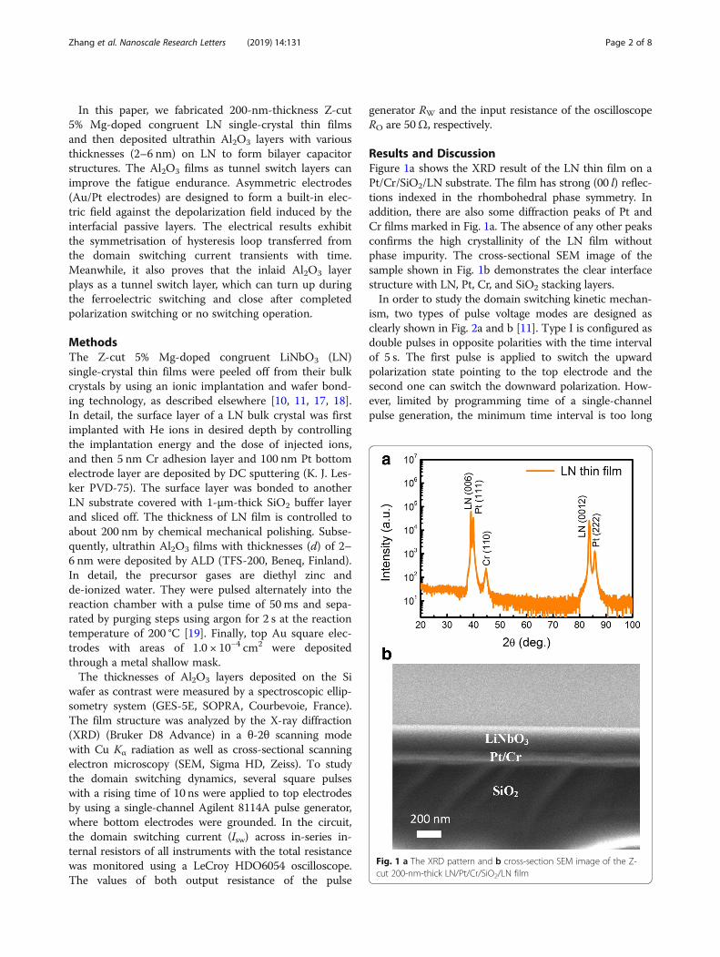
Results and DiscussionFigure 1a shows the XRD result of the LN thin film on aPt/Cr/SiO2/LN substrate. The film has strong (00 l) reflec-tions indexed in the rhombohedral phase symmetry. Inaddition, there are also some diffraction peaks of Pt andCr films marked in Fig. 1a. The absence of any other peaksconfirms the high crystallinity of the LN film withoutphase impurity. The cross-sectional SEM image of thesample shown in Fig. 1b demonstrates the clear interfacestructure with LN, Pt, Cr, and SiO2 stacking layers.In order to study the domain switching kinetic mechan-
ism, two types of pulse voltage modes are designed asclearly shown in Fig. 2a and b [11]. Type I is configured asdouble pulses in opposite polarities with the time intervalof 5 s. The first pulse is applied to switch the upwardpolarization state pointing to the top electrode and thesecond one can switch the downward polarization. How-ever, limited by programming time of a single-channelpulse generation, the minimum time interval is too long
Fig. 1 a The XRD pattern and b cross-section SEM image of the Z-cut 200-nm-thick LN/Pt/Cr/SiO2/LN film
Zhang et al. Nanoscale Research Letters (2019) 14:131 Page 2 of 8
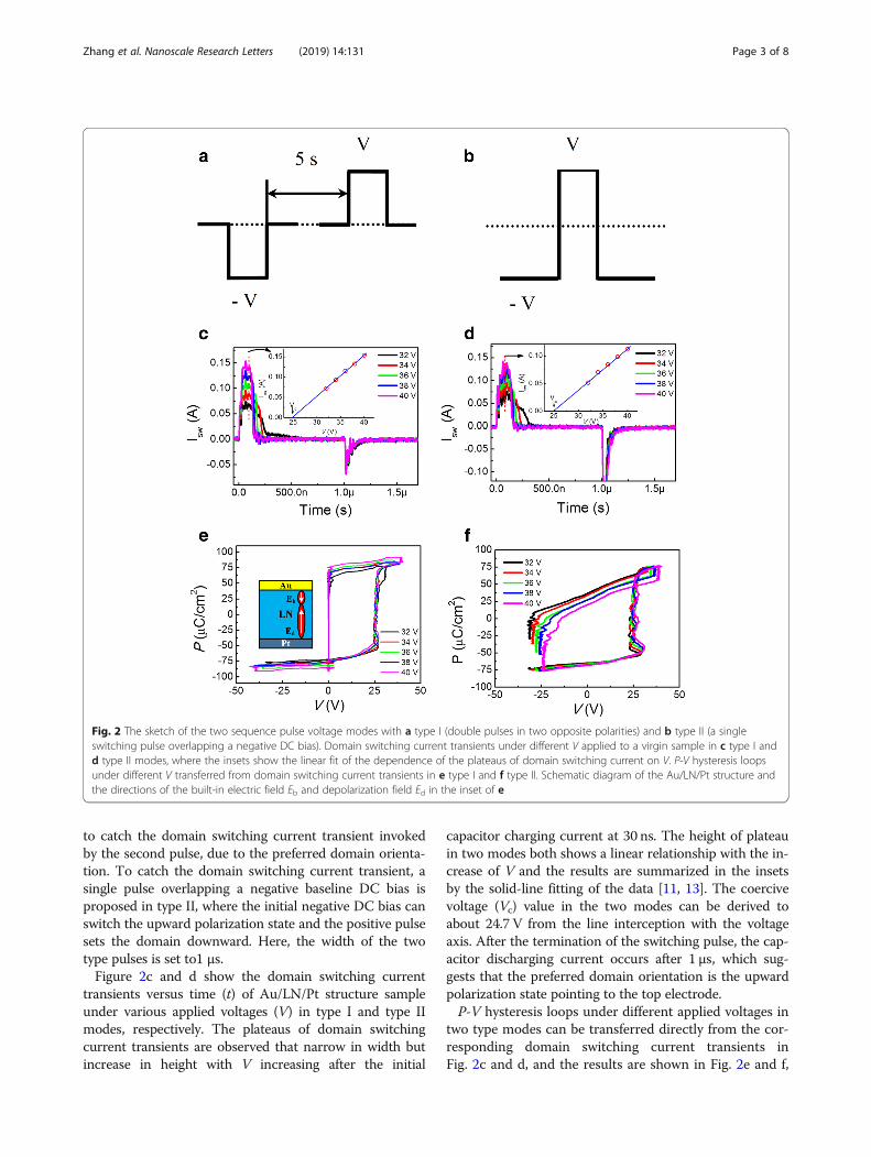
to catch the domain switching current transient invokedby the second pulse, due to the preferred domain orienta-tion. To catch the domain switching current transient, asingle pulse overlapping a negative baseline DC bias isproposed in type II, where the initial negative DC bias canswitch the upward polarization state and the positive pulsesets the domain downward. Here, the width of the twotype pulses is set to1 μs.Figure 2c and d show the domain switching current
transients versus time (t) of Au/LN/Pt structure sampleunder various applied voltages (V) in type I and type IImodes, respectively. The plateaus of domain switchingcurrent transients are observed that narrow in width butincrease in height with V increasing after the initial
capacitor charging current at 30 ns. The height of plateauin two modes both shows a linear relationship with the in-crease of V and the results are summarized in the insetsby the solid-line fitting of the data [11, 13]. The coercivevoltage (Vc) value in the two modes can be derived toabout 24.7 V from the line interception with the voltageaxis. After the termination of the switching pulse, the cap-acitor discharging current occurs after 1 μs, which sug-gests that the preferred domain orientation is the upwardpolarization state pointing to the top electrode.P-V hysteresis loops under different applied voltages in
two type modes can be transferred directly from the cor-responding domain switching current transients inFig. 2c and d, and the results are shown in Fig. 2e and f,
Fig. 2 The sketch of the two sequence pulse voltage modes with a type I (double pulses in two opposite polarities) and b type II (a singleswitching pulse overlapping a negative DC bias). Domain switching current transients under different V applied to a virgin sample in c type I andd type II modes, where the insets show the linear fit of the dependence of the plateaus of domain switching current on V. P-V hysteresis loopsunder different V transferred from domain switching current transients in e type I and f type II. Schematic diagram of the Au/LN/Pt structure andthe directions of the built-in electric field Eb and depolarization field Ed in the inset of e
Zhang et al. Nanoscale Research Letters (2019) 14:131 Page 3 of 8
respectively [11, 20]. A determined forward coercivevoltage of about 25 V invariable with V is obtained inthe two types pulses. The coercive voltage approaches toVc extracted from the linear Isw-V plot in the inset ofFig. 2c and d. Unlike the non-doped LN film, the Vc isvariable and the value is equal to the maximum appliedvoltages [10]. For the 5% Mg-doped LN, the defined Vc isinvariable with V, as shown in Fig. 2e and f. This is be-cause the Mg doping can generate Li-site metal vacanciesand oxygen vacancy-related defects, [21–23] which cantrap space charges and effectively shorten the resistancedegradation time across the interfacial layers between thefilm and top/bottom electrodes [11]. Therefore, domainswitching currents overlap with capacitor charging cur-rents in acceleration of domain switching speed with adefinite Vc, as shown in Fig. 2c and d. However, limited bythe pulse generator, the output baseline voltage in type IImode cannot be shift symmetrically when increasing ap-plied pulse voltage over 32 V. Compared to the imprintedloops along the positive voltage axis in Fig. 2e, the symme-trisation of the loops are achieved along the voltage axis inFig. 2f, different from those in Pt/LiNbO3/Pt structureswhere the P-V hysteresis loops in either type I or type IIare imprinted toward a positive voltage [11]. The reasonof the symmetrical P-V loops in Fig. 2f may be attributedto the designed asymmetric electrodes (here Au/Pt). Thework function of Au electrode is 5.1 eV, which is slightlysmaller than that of Pt (5.65 eV) [24]. There will induce abuilt-in electric field (Eb) with the direction pointing fromthe top electrode to the bottom electrode, shown in theinset of Fig. 2e. The depolarization field (Ed) induced bythe interfacial passive layers has the opposite direction toEb. The Ed can switch back the polarization in a very shorttime after the termination of the switching pulse in type IIfor the symmetrical electrodes (Pt/Pt) [11]. In our experi-ment, the Eb can partially screen the Ed and accumulateinjected charges in compensation of an internal imprintfield, [16] which can slow down the backswitching time.Hence, the switched domain can maintain and back-switching current transient will be captured by type IIpulse. However, the time interval of the two pulses withopposite polarities in type I mode is too long. After thefirst pulse, the trapped injected charges by Eb will be grad-ually driven out of the film by Ed before the arrival of thesecond pulse in type I [11]. In order to prove the attribu-tion of built-in electric field to the symmetrisation of theloops, Pt/LiNbO3/Pt symmetrical structure sample wasprepared and the imprinted loops along the positive volt-age axis were transferred directly from the correspondingdomain switching current transients in Additional file 1:Figure S1a at positive pulse with voltages/widths of 30–40V/500 ns, shown in Additional file 1: Figure S1b.Figure 3a and b show the domain switching current
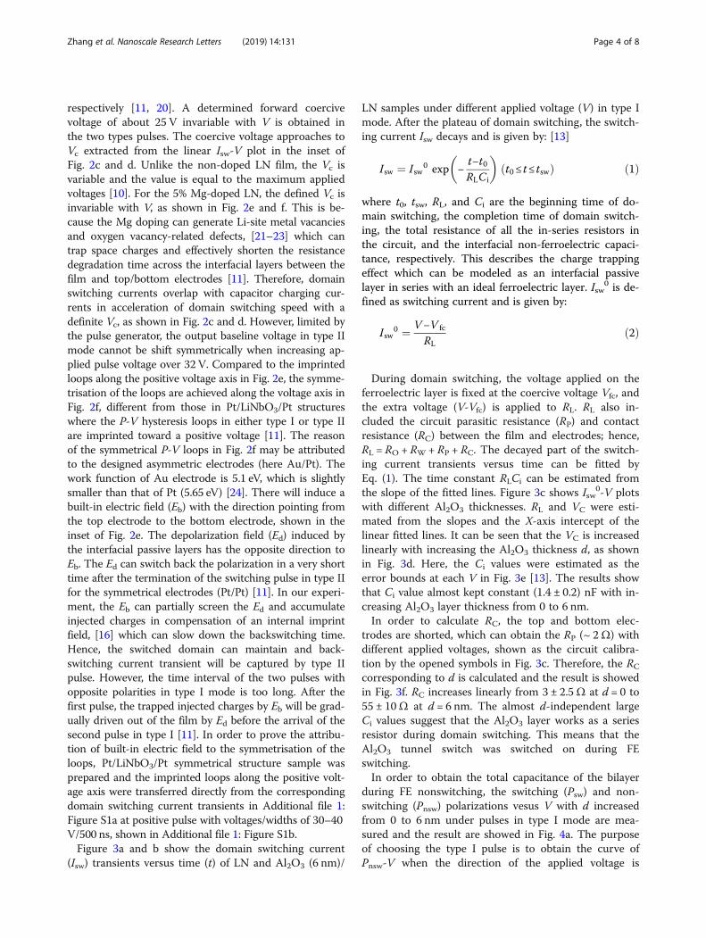
(Isw) transients versus time (t) of LN and Al2O3 (6 nm)/
LN samples under different applied voltage (V) in type Imode. After the plateau of domain switching, the switch-ing current Isw decays and is given by: [13]
Isw ¼ Isw0 exp −
t−t0RLCi
� �t0≤ t≤tswð Þ ð1Þ
where t0, tsw, RL, and Ci are the beginning time of do-main switching, the completion time of domain switch-ing, the total resistance of all the in-series resistors inthe circuit, and the interfacial non-ferroelectric capaci-tance, respectively. This describes the charge trappingeffect which can be modeled as an interfacial passivelayer in series with an ideal ferroelectric layer. Isw
0 is de-fined as switching current and is given by:
Isw0 ¼ V−V fc
RLð2Þ
During domain switching, the voltage applied on theferroelectric layer is fixed at the coercive voltage Vfc, andthe extra voltage (V-Vfc) is applied to RL. RL also in-cluded the circuit parasitic resistance (RP) and contactresistance (RC) between the film and electrodes; hence,RL = RO + RW + RP + RC. The decayed part of the switch-ing current transients versus time can be fitted byEq. (1). The time constant RLCi can be estimated fromthe slope of the fitted lines. Figure 3c shows Isw
0-V plotswith different Al2O3 thicknesses. RL and VC were esti-mated from the slopes and the X-axis intercept of thelinear fitted lines. It can be seen that the VC is increasedlinearly with increasing the Al2O3 thickness d, as shownin Fig. 3d. Here, the Ci values were estimated as theerror bounds at each V in Fig. 3e [13]. The results showthat Ci value almost kept constant (1.4 ± 0.2) nF with in-creasing Al2O3 layer thickness from 0 to 6 nm.In order to calculate RC, the top and bottom elec-
trodes are shorted, which can obtain the RP (~ 2Ω) withdifferent applied voltages, shown as the circuit calibra-tion by the opened symbols in Fig. 3c. Therefore, the RC
corresponding to d is calculated and the result is showedin Fig. 3f. RC increases linearly from 3 ± 2.5Ω at d = 0 to55 ± 10Ω at d = 6 nm. The almost d-independent largeCi values suggest that the Al2O3 layer works as a seriesresistor during domain switching. This means that theAl2O3 tunnel switch was switched on during FEswitching.In order to obtain the total capacitance of the bilayer
during FE nonswitching, the switching (Psw) and non-switching (Pnsw) polarizations vesus V with d increasedfrom 0 to 6 nm under pulses in type I mode are mea-sured and the result are showed in Fig. 4a. The purposeof choosing the type I pulse is to obtain the curve ofPnsw-V when the direction of the applied voltage is
Zhang et al. Nanoscale Research Letters (2019) 14:131 Page 4 of 8
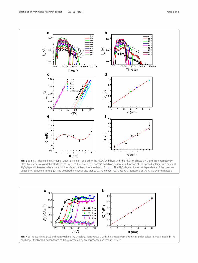
Fig. 3 a, b Isw-t dependences in type I under different V applied to the Al2O3/LN bilayer with the Al2O3 thickness d = 0 and 6 nm, respectively,fitted by a series of parallel dotted lines to Eq. (1). c The plateaus of domain switching current as a function of the applied voltage with differentAl2O3 layer thicknesses, where the solid lines show the best fit of the data to Eq. (2). d The Al2O3-layer-thickness d dependence of the coercivevoltage (Vc) extracted from c. e, f The extracted interfacial capacitance Ci and contact resistance RC as functions of the Al2O3 layer thickness d
Fig. 4 a The switching (Psw) and nonswitching (Pnsw) polarizations versus V with d increased from 0 to 6 nm under pulses in type I mode. b TheAl2O3-layer-thickness d dependence of 1/Ctot measured by an impedance analyzer at 100 kHz
Zhang et al. Nanoscale Research Letters (2019) 14:131 Page 5 of 8
consistent with the polarization orientation, from whichthe total capacitance (Ctot) of the bilayer can be calcu-lated from the relation, Ctot = S·dPnsw/dV, where S is theelectrode area. It can totally exclude the charge effectsby FE switching in the type I pulse mode, but using thetype II mode cannot achieve this effect with the negativeswitching polarization, which can switch back thepolarization involved with the charges injection. The dif-ference between Psw and Pnsw is 2Pr, as shown in Fig. 4a.It has small change with d from 0 to 6 nm, whereas thePnsw (open symbols) signals are too weak to be moni-tored by an oscilloscope. To prove the Al2O3 tunnelswitch layer working as a dielectric capacitor, the directCtot measurements using a low-frequency impedanceanalyzer at 100 kHz with no additional DC bias werecarried out and their results are shown in Fig. 4b, whichcan be fitted by Eq. (3):
1Ctot
¼ 1C f
þ dε0εAlS
ð3Þ
where εAl is the dielectric constant of the Al2O3 layerand ε0 is the vacuum permittivity of free space. Cf and Srepresent the capacitance of the ferroelectric layer andthe electrode area, respectively. Figure 4b shows the lin-ear 1/Ctot versus d plot, which suggests that the Al2O3
layer becomes a highly insulating dielectric film undernonswitching situation or post-switching. It can be de-rived that Cf ≈ 14 pF and εAl ≈ 7.9 from Eq. (3). There-fore, the interposed thin Al2O3 layer is proved as adielectric capacitor. During FE nonswitching as well asafter FE switching, the Al2O3 tunnel switch closes as aninsulator.
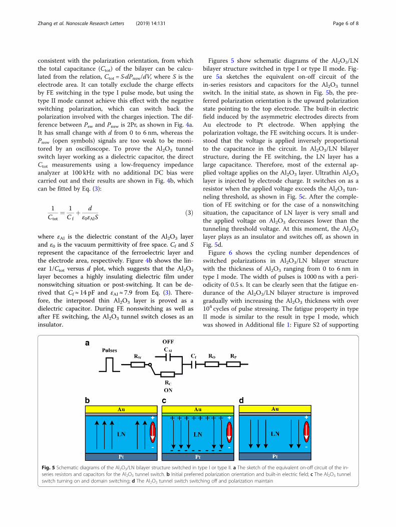
Figures 5 show schematic diagrams of the Al2O3/LNbilayer structure switched in type I or type II mode. Fig-ure 5a sketches the equivalent on-off circuit of thein-series resistors and capacitors for the Al2O3 tunnelswitch. In the initial state, as shown in Fig. 5b, the pre-ferred polarization orientation is the upward polarizationstate pointing to the top electrode. The built-in electricfield induced by the asymmetric electrodes directs fromAu electrode to Pt electrode. When applying thepolarization voltage, the FE switching occurs. It is under-stood that the voltage is applied inversely proportionalto the capacitance in the circuit. In Al2O3/LN bilayerstructure, during the FE switching, the LN layer has alarge capacitance. Therefore, most of the external ap-plied voltage applies on the Al2O3 layer. Ultrathin Al2O3
layer is injected by electrode charge. It switches on as aresistor when the applied voltage exceeds the Al2O3 tun-neling threshold, as shown in Fig. 5c. After the comple-tion of FE switching or for the case of a nonswitchingsituation, the capacitance of LN layer is very small andthe applied voltage on Al2O3 decreases lower than thetunneling threshold voltage. At this moment, the Al2O3
layer plays as an insulator and switches off, as shown inFig. 5d.Figure 6 shows the cycling number dependences of
switched polarizations in Al2O3/LN bilayer structurewith the thickness of Al2O3 ranging from 0 to 6 nm intype I mode. The width of pulses is 1000 ns with a peri-odicity of 0.5 s. It can be clearly seen that the fatigue en-durance of the Al2O3/LN bilayer structure is improvedgradually with increasing the Al2O3 thickness with over104 cycles of pulse stressing. The fatigue property in typeII mode is similar to the result in type I mode, whichwas showed in Additional file 1: Figure S2 of supporting
Fig. 5 Schematic diagrams of the Al2O3/LN bilayer structure switched in type I or type II. a The sketch of the equivalent on-off circuit of the in-series resistors and capacitors for the Al2O3 tunnel switch. b Initial preferred polarization orientation and built-in electric field; c The Al2O3 tunnelswitch turning on and domain switching; d The Al2O3 tunnel switch switching off and polarization maintain
Zhang et al. Nanoscale Research Letters (2019) 14:131 Page 6 of 8
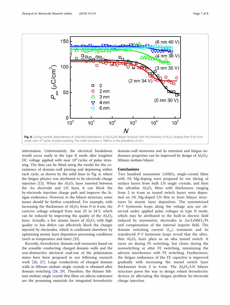
information. Unfortunately, the electrical breakdownwould occur easily in the type II mode after longtimeDC voltage applied with near 104 cycles of pulse stres-sing. The data can be fitted using the model for the co-existence of domain-wall pinning and depinning withineach cycle, as shown by the solid lines in Fig. 6, wherethe fatigue physics was attributed to by-electrode chargeinjection [13]. When the Al2O3 layer inserted betweenthe Au electrode and LN layer, it can block theby-electrode injection charge path and improve the fa-tigue endurance. However, in the bilayer structure, someissues should be further considered. For example, withincreasing the thicknesses of Al2O3 from 0 to 6 nm, thecoercive voltage enlarged from near 25 to 34 V, whichcan be reduced by improving the quality of the Al2O3
layer. Actually, a few atomic layers of Al2O3 with highquality or less defect can effectively block the chargesinjected by electrodes, which is confirmed elsewhere byoptimizing atomic layer deposition processing conditions(such as temperature and time) [25].Recently, ferroelectric domain-wall memories based on
the erasable conducting charged domain walls and thenon-destructive electrical read-out of the polarizationstates have been proposed in our following researchwork [26, 27]. Large conductivity of charged domainwalls in lithium niobate single crystals is obtained afterdomain switching [28, 29]. Therefore, the thinner lith-ium niobate single crystal thin films on silicon substratesare the promising materials for integrated ferroelectric
domain-wall memories and its retention and fatigue en-durance properties can be improved by design of Al2O3/lithium niobate bilayer.
ConclusionsTwo hundred nanometer LiNbO3 single-crystal filmswith 5% Mg-doping were prepared by ion slicing ofsurface layers from bulk LN single crystals, and thenthe ultrathin Al2O3 films with thicknesses rangingfrom 2 to 6 nm as tunnel switch layers were depos-ited on 5% Mg-doped LN film to form bilayer struc-tures by atomic layer deposition. The symmetrizedP-V hysteresis loops along the voltage axis are ob-served under applied pulse voltages in type II mode,which may be attributed to the built-in electric fieldinduced by asymmetric electrodes in Au/LiNbO3/Ptand compensation of the internal imprint field. Thedomain switching current (Isw) transients and itstransferred P-V hysteresis loops reveal that the ultra-thin Al2O3 layer plays as an idea tunnel switch. Itturns on during FE switching, but closes during thenonswitching or after FE switching, minimizing theadverse interference with FE switching. Furthermore,the fatigue endurance of the FE capacitor is improvedgradually with increasing the tunnel switch layerthicknesses from 2 to 6 nm. The Al2O3/LN bilayerstructure paves the way to design robust ferroelectricdevices in alleviating the fatigue problem by-electrodecharge injection.
Fig. 6 Cycling number dependences of switched polarizations in Al2O3/LN bilayer structure with the thickness of Al2O3 ranging from 0 to 6 nmunder over 104 cycles of pulse stressing. The width of pulses is 1000 ns in the periodicity of 0.5 s
Zhang et al. Nanoscale Research Letters (2019) 14:131 Page 7 of 8
Additional file
Additional file 1: The imprinted P-V hysteresis loops of Pt/LiNbO3/Ptsymmetrical structure sample in type II mode and the fatigue property ofAl2O3/LiNbO3 bilayer structure in type II mode. (DOCX 144 kb)
AbbreviationsALD: Atomic layer deposition; CMOS: Complementary metal oxidesemiconductor; FE: Ferroelectric; LN: Lithium niobate; SEM: Scanning electronmicroscopy; XRD: X-ray diffraction
AcknowledgementsThis work was supported by the National Natural Science Foundation ofChina (grant number 61674044), the Basic Research Project of ShanghaiScience and Technology Innovation Action (grant number 17JC1400300), theNational Key Basic Research Program of China (grant number2014CB921004), and the Program of Shanghai Subject Chief Scientist (grantnumber 17XD1400800).
Availability of Data and MaterialsThe datasets generated during and/or analyzed during the current study areavailable from the corresponding author on reasonable request.
Authors’ ContributionsYZ and QHR prepared the materials and draft the manuscript. AQJ, YZ, and JJdesigned the work. YZ, XJC, JGY, and QHR carried out the structural analysesand switching current measurements of the samples. AQJ edited the wholemanuscript. All authors had read and approved the final manuscript.
Competing InterestsThe authors declare that they have no competing interests.
Publisher’s NoteSpringer Nature remains neutral with regard to jurisdictional claims inpublished maps and institutional affiliations.
Received: 28 January 2019 Accepted: 3 April 2019
References1. Fujiwara T, Takahashi M, Ohama M, Ikushima AJ, Furukawa Y, Kitamura K
(1999) Comparison of electro-optic effect between stoichiometric andcongruent LiNbO3. Electron Lett 35:499–501
2. Volk TR, Gainutdinov RV, Zhang HH (2017) Domain-wall conduction inAFM-written domain patterns in ion-sliced LiNbO3 films. Appl Phys Lett110:132905
3. Poberaj G, Hu H, Sohler W, Gunter P (2012) Lithium niobate on insulator(LNOI) for micro-photonic devices. Laser Photonics Rev 6:488–503
4. Cho YS, Fujimoto K, Hiranaga Y, Wagatsuma Y, Onoe A, Terabe K, KitamuraK (2002) Tbit/inch2 ferroelectric data storage based on scanning nonlineardielectric microscopy. Appl Phys Lett 81:4401–4403
5. Wang C, Burek MJ, Lin Z, Atikian HA, Venkataraman V, Huang IC, Stark P,Loncar M (2014) Integrated high quality factor lithium niobate microdiskresonators. Opt Express 22:30924–30933
6. Gainutdinov RV, Volk TR, Zhang HH (2015) Domain formation andpolarization reversal under atomic force microscopy-tip voltages in ion-sliced LiNbO3 films on SiO2/LiNbO3 substrates. Appl Phys Lett 107:162903
7. Hu H, Yang J, Gui L, Sohler W (2012) Lithium niobate-on-insulator (LNOI):status and perspectives. Proc SPIE 8431:84311D
8. Wang C, Zhang M, Chen X, Bertrand M, Shams-Ansari A, Chandrasekhar S,Winzer P, Loncar M (2018) Integrated lithium niobate electro-opticmodulators operating at CMOS-compatible voltages. Nature 562:101–104
9. Tanaka S, Park K, Esashi M (2012) Lithium-niobate-based surface acousticwave oscillator directly integrated with CMOS sustaining amplifier. Ieee TUltrason Ferr 59:1800–1805
10. Jiang J, Meng XJ, Geng DQ, Jiang AQ (2015) Accelerated domain switchingspeed in single-crystal LiNbO3 thin films. J Appl Phys 117:104101
11. Zhang Y, Jiang AQ (2018) Low-frequency charge trapping and bistabledomain switching in Mg-doped LiNbO3 single crystal films. J Appl Phys 124:124103
12. Jiang AQ, Lin YY, Tang TA (2007) Unsaturated charge injection at high-frequency fatigue of Pt/Pb (Zr,Ti)O3/Pt thin-film capacitors. Appl Phys Lett91:082901
13. Jiang AQ, Lee HJ, Hwang CS, Scott JF (2012) Sub-picosecond processes offerroelectric domain switching from field and temperature experiments.Adv Funct Mater 22:192–199
14. Jiang AQ, Lee HJ, Kim GH, Hwang CS (2009) The inlaid Al2O3 tunnel switchfor ultrathin ferroelectric films. Adv Mater 21:2870–2875
15. Lee HJ, Kim GH, Park MH, Jiang AQ, Hwang CS (2010) Polarization reversalbehavior in the Pt/Pb (Zr,Ti)O3/Pt and Pt/Al2O3/Pb (Zr,Ti)O3/Pt capacitors fordifferent reversal directions. Appl Phys Lett 96:212902
16. Lee HJ, Park MH, Kim YJ, Hwang CS, Kim JH, Funakubo H, Ishiwara H (2011)Improved ferroelectric property of very thin Mn-doped BiFeO3 films by aninlaid Al2O3 tunnel switch. J Appl Phys 10:074111
17. Levy M, Osgood RM, Liu R, Cross LE, Cargill GS, Kumar A, Bakhru H (1998)Fabrication of single-crystal lithium niobate films by crystal ion slicing. ApplPhys Lett 73:2293–2295
18. Han HP, Cai LT, Xiang BX, Jiang YP, Hu H (2015) Lithium-rich vapor transportequilibration in single-crystal lithium niobate thin film at low temperature.Opt Mater Express 5:2634–2641
19. Ren QH, Zhang Y, Lu HL, Chen HY, Zhang Y, Li DH, Liu WJ, Ding SJ, JiangAQ, Zhang DW (2016) Surface-plasmon mediated photoluminescenceenhancement of Pt-coated ZnO nanowires by inserting an atomic-layer-deposited Al2O3 spacer layer. Nanotechnology 27:165705
20. Jiang AQ, Liu XB, Zhang Q (2011) Nanosecond-range imprint and retentioncharacterized from polarization-voltage hysteresis loops in insulating orleaky ferroelectric thin films. Appl Phys Lett 99:142905
21. Nakamura M, Higuchi S, Takekawa S, Terabe K, Furukawa Y, Kitamura K(2002) Optical damage resistance and refractive indices in near-stoichiometric MgO-doped LiNbO3. Jpn J Appl Phys 41:L49–L51
22. Furukawa Y, Kitamura K, Takekawa S, Miyamoto A, Terao M, Suda N (2000)Photorefraction in LiNbO3 as a function of [Li]/[Nb] and MgOconcentrations. Appl Phys Lett 77:2494–2496
23. Furukawa Y, Kitamura K, Takekawa S, Niwa K, Yajima Y, Iyi N, Mnushkina I,Guggenheim P, Martin JM (2000) The correlation of MgO-doped near-stoichiometric LiNbO3 composition to the defect structure. J Cryst Growth211:230–236
24. Pintilie L, Vrejoiu I, Hesse D, Alexe M (2008) The influence of the top-contactmetal on the ferroelectric properties of epitaxial ferroelectric Pb (Zr0.2Ti0.8)O3 thin films. J Appl Phys 104:114101
25. Wilt J, Sakidja R, Goul R, Wu JZ (2017) Effect of an interfacial layer onelectron tunneling through atomically thin Al2O3 tunnel barriers. ACS ApplMater Interfaces 9:37468–37475
26. Jiang J, Bai ZL, Chen ZH, He L, Zhang DW, Zhang QH, Shi JA, Park MH, ScottJF, Hwang CS, Jiang AQ (2018) Temporary formation of highly conductingdomain walls for non-destructive read-out of ferroelectric domain-wallresistance switching memories. Nat Mater 17:49–56
27. Ma J, Ma J, Zhang QH, Peng RC, Wang J, Liu C, Wang M, Li N, Chen MF,Cheng XX, Gao P, Gu L, Chen LQ, Yu P, Zhang JX, Nan CW (2018)Controllable conductive readout in self-assembled, topologically confinedferroelectric domain walls. Nat Nanotechnol 13:947–952
28. Werner CS, Herr SJ, Buse K, Sturman B, Soergel E, Razzaghi C, Breunig I(2017) Large and accessible conductivity of charged domain walls in lithiumniobate. Sci Rep 7:9862
29. Godau C, Kampfe T, Thiessen A, Eng LM, Haussmann A (2017) Enhancingthe domain wall conductivity in lithium niobate single crystals. ACS Nano11:4816–4824
Zhang et al. Nanoscale Research Letters (2019) 14:131 Page 8 of 8


![Localized Holographic Recording in doubly doped Lithium ...LiNbO3 [1]. The technique is based on the recording oflocalized holograms in thin layers across the volume ofthe crystal](https://img.pdfslide.us/doc/110x75/5e9706003ad76c38971939f3/localized-holographic-recording-in-doubly-doped-lithium-linbo3-1-the-technique.jpg)


![FERROELECTRIC RAM [FRAM]](https://img.pdfslide.us/doc/110x75/56816799550346895ddcd567/ferroelectric-ram-fram.jpg)