Embed Size (px)
Citation preview

Application ReportSPRAA99–March 2008
nFBGA PackagingRobert Furtaw..................................................................................................................................
ABSTRACTThis application report gives you technical background on nFBGA packages andexplains how to use them to build advanced board layouts.
Contents1 Introduction .......................................................................................... 32 PCB Design Considerations....................................................................... 53 Reliability ........................................................................................... 104 Surface-Mounting nFBGA Packages ........................................................... 155 Packing and Shipping ............................................................................ 196 Sockets ............................................................................................. 26Appendix A Frequently Asked Questions ........................................................... 33Appendix B Package Data Sheets ................................................................... 35Appendix C Thermal Modeling Results ............................................................. 64
List of Figures
1 Packaging Trends .................................................................................. 32 Structure of TI’s nFBGA Package ................................................................ 43 nFBGA Package Assembly Flow ................................................................. 44 Package Via to Board Land Area Configuration................................................ 55 Effects of Via-to-Land Ratios...................................................................... 56 Optimum Land Configurations .................................................................... 67 PCB Design Considerations (Conventional) .................................................... 78 Microvia Structure .................................................................................. 89 "Dog Bone" Via Structure.......................................................................... 810 Buried Vias .......................................................................................... 911 Daisy-Chained Pinout List (195ZWV nFBGA Package) ..................................... 1012 PCB Layout for Daisy-Chained Unit ............................................................ 1113 Daisy-Chain Test Configuration ................................................................. 1114 Thermal Modeling Process ...................................................................... 1515 Solder Ball Collapse .............................................................................. 1716 Recommended Reflow Profile of Pb-Free nFBGA Package ................................ 1817 Recommended Reflow Profile of Eutectic SnPb nFBGA Package ......................... 1918 Shipping Tray Detail .............................................................................. 2019 Single Sprocket Tape Dimension ............................................................... 2420 Reel Dimensions .................................................................................. 2521 Tape-and-Reel Packing .......................................................................... 2522 Approaches for Contacting the Solder Ball .................................................... 2723 Pinch Contact for Solder Ball .................................................................... 2824 Contact Area on Solder Ball ..................................................................... 2925 Witness Marks on Solder Ball ................................................................... 3026 Effect of Bur-In on Probe Mark .................................................................. 3127 Micro Tuning Fork Contact for 0.5mm Pitch................................................... 3128 Micro Tuning Fork Contact and Contact Marks on Solder Balls ............................ 32
SPRAA99–March 2008 nFBGA Packaging 1Submit Documentation Feedback

www.ti.com
29 Socket Examples: Tuning Fork (Left) and Pinch Style (Right) .............................. 32B-1 87ZVW Package Outline (6 x 6mm, 0.5mm pitch)............................................ 37B-2 72ZST Package Outline (7 x 7mm, 0.5mm pitch) ............................................ 38B-3 143ZZC Package Outline (7 x 7mm, 0.5mm pitch)........................................... 39B-4 143ZWU Package Outline (7 x 7mm, 0.5mm pitch) .......................................... 40B-5 143ZWU Daisy Chain Net List................................................................... 40B-6 152ZZB Package Outline (7 x 7mm, 0.5mm pitch) ........................................... 41B-7 209ZXN Package Outline (7 x 7mm, 0.4mm pitch)........................................... 42B-8 113ZVD Package Outline (8 x 8mm, 0.65mm pitch) ......................................... 43B-9 113ZVD Daisy Chain Net List ................................................................... 43B-10 195ZWV Package Outline (8 x 8mm, 0.5mm pitch) .......................................... 44B-11 195ZWV Daisy Chain Net List................................................................... 44B-12 225ZWF Package Outline (10 x 10mm, 0.5mm pitch) ....................................... 45B-13 241ZWG Package Outline (10 x 10mm, 0.5mm pitch)....................................... 46B-14 241ZWJ Package Outline (10x10mm, 0.4mm pitch) ......................................... 47B-15 241ZWJ Daisy Chain Net List ................................................................... 47B-16 289ZWJ Package Outline (10 x 10mm, 0.4mm pitch) ....................................... 48B-17 289ZWJ Daisy Chain Net List ................................................................... 49B-18 360ZWJ Package Outline (10 x 10mm, 0.4mm pitch) ....................................... 50B-19 360ZWJ Daisy Chain Net List ................................................................... 50B-20 145ZWS Package Outline (12 x 12mm, 0.8mm pitch) ....................................... 51B-21 289ZVL Package Outline (12 x 12mm, 0.5mm pitch) ........................................ 52B-22 293ZVL Package Outline (12 x 12mm, 0.5mm pitch) ........................................ 53B-23 318ZVL Package Outline (12 x 12mm, 0.5mm pitch) ........................................ 54B-24 325ZVL Package Outline (12 x 12mm, 0.5mm pitch) ........................................ 55B-25 325ZVL Daisy Chain Net List.................................................................... 56B-26 385ZWM Package Outline (12 x 12mm, 0.5mm pitch)....................................... 57B-27 385ZWK Package Outline (12 x 12mm, 0.5mm pitch) ....................................... 58B-28 385ZWK Daisy Chain Net List................................................................... 58B-29 289ZWE Package Outline (13 x 13mm, 0.5mm pitch) ....................................... 59B-30 447ZAC Package Outline (14 x 14mm, 0.5mm pitch)........................................ 60B-31 447ZAF Package Outline (14 x 14mm, 0.5mm pitch) ........................................ 61B-32 361ZWT Package Outline (16 x 16mm, 0.8mm pitch) ....................................... 62B-33 361ZWT Daisy Chain Net List................................................................... 62
List of Tables
1 Package-Level Reliability Tests ................................................................. 112 Package-Level Reliability Test Results......................................................... 123 Board-Level Reliability Summary ............................................................... 134 Summary of Significant BLR Improvements................................................... 135 Effects of Pad Size and Board Thickness on Fatigue Life................................... 146 Number of Units per Shipping Tray............................................................. 207 Tape Dimensions.................................................................................. 248 Reel Dimensions .................................................................................. 25B-1 TI’s Strategic Package Line-Up ................................................................. 35C-1 8×8 mm nFBGA Thermal Simulation Result................................................... 64C-2 12×12 mm nFBGA Thermal Simulation Result................................................ 64C-3 16×16 mm nFBGA Thermal Simulation Result................................................ 65
PACED, ThermCAL are trademarks of Texas Instruments.All other trademarks are the property of their respective owners.
nFBGA Packaging2 SPRAA99–March 2008Submit Documentation Feedback

www.ti.com
1 Introduction
Package
siz
e
QFP0.5 mm pitch
BGA (ball grid array)1.27 mm ball pitch
Fine pitch requirement
QFP0.4 mm pitch
Bare chip(flip chip)
• Infra. issue (KGD)
• Soldering difficulties
• PWB/ASSY cost up
CSP (chip scale pkg.) solution
Fine pitch BGA(0.5, 0.8, 1.0 mm ball pitch)
QFP-0.5
QFP-0.4
CSP
BGA
Bare chip (bump)
Pin count
Package trend (customer requirement)
Introduction
The parallel pursuit of cost reduction and miniaturization in recent years has increased emphasis on verysmall integrated circuit (IC) package solutions. This is particularly evident in consumer-based endequipment using digital signal processor (DSP) solutions such as wireless telephones, laptop computers,and hard-disk drives. Despite the formal definition, packages with an area similar in size to the IC theyencapsulate are loosely referred to as chip scale packages (CSPs). Figure 1 illustrates this trend.
Figure 1. Packaging Trends
CSPs are in many ways an ideal solution to the cost reduction and miniaturization requirements. Theyoffer enormous area reductions compared to quad flat packages (QFPs) and have increasing potential todo so without adding to system-level cost. In the best case, CSPs compete today on a cost-per-terminalbasis with QFPs. Various CSPs from Texas Instruments (TI) are now available at cost parity with thinQFPs.
Texas Instruments produces a laminate-based family of CSPs known as New Fine Pitch Ball Grid Arraypackages (also referred to as nFBGA packages). Like most other CSPs, nFBGA packages use solderalloy balls as the interconnect between the package substrate and the board on which the package issoldered. The nFBGA family comes in a range of solder ball pitch, and can accommodate various stackeddie configurations, with as many as three die housed in each package. Figure 2 shows the structure ofTI’s nFBGA package.
SPRAA99–March 2008 nFBGA Packaging 3Submit Documentation Feedback

www.ti.com
Wire bond
Silicon Die
Laminate Substrate
Solder Ball Array
Die Attach Material
Encapsulant
Same as QFP assembly
Die attach Wire bond Encap
Non-Ag paste Short loop X’fer mode
Ball attach IR reflow Flux wash
0.30 mm DIA. Ultrasonic clean
Laser symbol
and singulation Test
Tray
BGA unique process
Introduction
Figure 2. Structure of TI’s nFBGA Package
Texas Instruments addressed several key issues in package assembly to produce a CSP that is not onlyphysically and mechanically stable but cost-effective for a wide variety of applications. Figure 3 shows ageneral flow used to produce TI nFBGA packages.
Figure 3. nFBGA Package Assembly Flow
4 nFBGA Packaging SPRAA99–March 2008Submit Documentation Feedback

www.ti.com
2 PCB Design Considerations
2.1 Solder Land Areas
nFBGA package
Land on PCBPackageball via
PCB
A
B
(Not to scale)
A = Via diameter on packageB = Land diameter on PCB
Ratio A/B should equal 1.0 for optimum reliability.
Package
PCB
Package
Package
PCB
PCB
PCB Design Considerations
The nFBGA package has been fully qualified in numerous applications and is being used extensively inmobile phones, laptops, modems, handheld devices, and office environment equipment. Your local TI fieldsales office can give you more information on using reliable and cost-effective nFBGA packaging in yourapplication.
Designs of both the nFBGA package itself and the printed circuit board (PCB) are important in achievinggood manufacturability and optimum reliability. In particular, the diameters of the package vias and theboard lands are critical. While the actual sizes of these dimensions are important, their ratio is morecritical. Figure 4 illustrates the package via-to-PCB configuration and Figure 5 illustrates why this ratio iscritical.
Figure 4. Package Via to Board Land Area Configuration
Figure 5. Effects of Via-to-Land Ratios
SPRAA99–March 2008 nFBGA Packaging 5Submit Documentation Feedback

www.ti.com
B
A
SMD
Solder Mask Defined
A
NSMD
Non-Solder Mask Defined
BallPitch
SMType
Thickness Opening
PWB Design Stencil Design
A B
SMD
NSMD0.4
0.25
0.28
0.30
0.23
0.08
0.08
0.25
0.23
SMD
NSMD0.5
0.30
0.30
0.35
0.25
0.10
0.10
0.30
0.30
SMD
NSMD0.65
0.35
0.35
0.40
0.30
0.12
0.12
0.35
0.35
SMD
NSMD0.8
0.40
0.40
0.45
0.35
0.15
0.15
0.40
0.40
SMD
NSMD1.0
0.45
0.45
0.50
0.40
0.15
0.15
0.45
0.45
All dimensions in mm.
Note:
It is not recommended to use “U” shape PWB land because of trappingvoid during reflow.
B
2.2 Conductor Width/Spacing
PCB Design Considerations
In the top view of Figure 5, the package via is larger than the PCB via, and the solder ball is prone tocrack prematurely at the PCB interface. In the middle view, the PCB via is larger than the package via,which leads to cracks at the package surface. In the bottom view, where the ratio is almost 1:1, thestresses are equalized and neither site is more susceptible to cracking than the other.
Solder lands on the PCB are generally simple round pads. Solder lands are either solder-mask-defined ornon-solder-mask-defined.• Solder-mask-defined (SMD) land. With this method, the copper pad is made larger than the desired
land area, and the opening size is defined by the opening in the solder mask material. The advantagesnormally associated with this technique include more closely controlled size and better copperadhesion to the laminate. Better size control is the result of photo imaging the stencils for masks. Thechief disadvantage of this method is that the larger copper spot can make routing more difficult.
• Non-solder-mask-defined (NSMD) land. Here, the land area is etched inside the solder mask area.While the size control is dependent on copper etching and is not as accurate as the solder maskmethod, the overall pattern registration is dependent on copper artwork, which is quite accurate. Thetradeoff is between accurate dot placement and accurate dot size.
See Figure 6 for an example of optimum land diameters and configurations for a common nFBGA pitch.
Figure 6. Optimum Land Configurations
Many of today’s circuit board layouts are based on at most a 100-µm conductor line width and 200-µmspacing. To route between 0.5-mm-pitch balls, given a clearance of roughly 190 µm between ball lands,only one signal can be routed between ball pads. The 200-µm ball spacing is worst case and is calculatedby assuming the diameter of the solder ball land is 410 µm.
6 nFBGA Packaging SPRAA99–March 2008Submit Documentation Feedback

www.ti.com
0.5 mmpitch
0.65 mmpitch
0.300 mmDIA. pad
0.35 mm DIA.solder mask
opening
0.254 mmDIA. hole
NSMD pads NSMD pads
0.350 mmDIA. pad
0.400 mm DIA.solder mask
opening
0.254 mmDIA. hole
0.250 mm DIA.solder mask
opening
SMD pads
0.300 mmDIA. pad
0.350 mmDIA. pad
0.300 mm DIA.solder mask
opening
SMD pads
(Not to scale)
0.1
25 m
m lin
e0.1
25 m
m lin
e
PC
BT
race
PC
BT
race
2.3 High-Density Routing Techniques
PCB Design Considerations
Figure 7 presents some design considerations based on commonly used PCB design rules.Conventionally, the pads are connected by wide copper traces to other devices or to plated through holes(PTH). As a rule, the mounting pads must be isolated from the PTH. Placing the PTH interstitially to theland pads often achieves this.
Figure 7. PCB Design Considerations (Conventional)
A challenge when designing with CSP packages is that as available space contracts, the space availablefor signal fanout also decreases. Routing of nFBGA packages can be especially challenging because ofthe tight ball pitch and a full array of solder balls that most packages have. By using a few high-densityrouting techniques, the PCB designer can minimize many of these design and manufacturing challenges.
SPRAA99–March 2008 nFBGA Packaging 7Submit Documentation Feedback

www.ti.com
2.4 Via Density
2.5 Conventional PCB Design
Cross-sectional view Top side view
Layer 1Layer 2Layer 3Layer 4Layer 5Layer 6
PCB Design Considerations
Via density, as mentioned earlier, can be a limiting factor when designing high-density boards. Via densityis defined as the number of vias in a particular board area. Using smaller vias increases the routability ofthe board by requiring less board space and increasing via density. The invention of the microvia, shownin Figure 8, has solved many of the problems associated with via density.
Figure 8. Microvia Structure
Microvias are often created using a laser to penetrate the first few layers of dielectric. The laser canpenetrate a 4-mil-thick dielectric layer, creating the 4 µm microvia shown in Figure 8. The layout designercan now route to the first internal board layer. Two layers (each 4 mils thick) can be laser-drilled, creatinga 200 µm microvia diameter. In this case, routing to the first two internal layers is possible.
The relatively large via density on the package periphery, mentioned earlier, is caused by limited optionswhen routing the signal from the ball. To reduce or eliminate the via density problem on the periphery ofthe package, designers can build the PCB vertically from the BGA pad through the internal layers of theboard, as shown in Figure 9. By working vertically and mechanically drilling 250 µm vias between the padson the board and the internal layers, designers can create a “pick-and-choose” method. They can pick thelayer and choose the route. A “dog bone” method is used to connect the through-hole via and the pad.This reduces the risk of trapped voids that can reduce the board mount process margin.
This method requires a very small mechanical drill to create the necessary number of vias for onepackage. Although this method is the least expensive, a disadvantage is that the vias go through theboard, creating a matrix of vias on the bottom side of the board, which may limit the use of using the backside for routing.
Figure 9. "Dog Bone" Via Structure
nFBGA Packaging8 SPRAA99–March 2008Submit Documentation Feedback

www.ti.com
2.6 Advanced Design Methods
Solder wicks intoblind via filling void
Micro blind viasLayer 1
Layer 2
Layer 3
Layer 4
Layer 5Layer 6
10-mil through-holeburied via
4-mil laser-drilled microvia may berequired to connect discretes onbottom side of board
PCB Design Considerations
Another option is to use a combination of blind and buried vias. Blind vias connect either the top or bottomside of the board to inner layers. Buried vias usually connect only the inner layers. Figure 10 illustratesthis method using 4-mil laser-drilled microvias in the center of the pads and burying the dog bone on layer2.
Figure 10. Buried Vias
Since the buried via does not extend through the underside of the board, the designer can use another setof laser-drilled blind microvias, if needed, to connect the bypass capacitors and other discrete componentsto the bottom side.
More information on these advanced techniques is available by contacting your local TI field sales office.
SPRAA99–March 2008 nFBGA Packaging 9Submit Documentation Feedback

www.ti.com
3 Reliability
3.1 Daisy-Chained Units
Reliability
Daisy-chained units are used to gain experience in the handling and mounting of CSPs for board-reliabilitytesting, to check PCB electrical layouts, and to confirm the accuracy of the mounting equipment. Tofacilitate this, Texas Instruments offers daisy-chained units in all production nFBGA packages.
Each daisy-chained pinout differs slightly depending on package layout. An example is shown inFigure 11. Daisy-chained packages are wired to provide a continuous path through the package for easytesting. TI issues a net list for each package, which correlates each ball position with a corresponding wirepad number. Examples of package net lists for production packages are included in Chapter B.
Figure 11. Daisy-Chained Pinout List (195ZWV nFBGA Package)
10 nFBGA Packaging SPRAA99–March 2008Submit Documentation Feedback

www.ti.com
Wire bonds
Solderballs
PCB
Copper traces
BGA Package
Test pads
Tester
Reliability
Figure 12 shows a PCB layout for an 80 GQE daisy-chained package. When a daisy-chained package isassembled on the PCB, a complete circuit is formed, which allows continuity testing. The circuit includesthe solder balls, the metal pattern on the die, the bond wires, and the PCB traces. The entire package oronly a quadrant can be interconnected and tested. A diagram of the test configuration is shown inFigure 13.
Figure 12. PCB Layout for Daisy-Chained Unit
Figure 13. Daisy-Chain Test Configuration
Reliability is one of the first questions designers ask about any new packaging technology. They want toknow how well the package will survive handling and assembly operation, and how long it will last on theboard. The elements of package reliability and system reliability, while related, focus on different materialproperties and characteristics and are tested by different methods.
Package reliability focuses on materials of construction, thermal flows, material adherence/delaminationissues, resistance to high temperatures, moisture resistance and ball/stitch bond reliability. Thoroughengineering of the package is performed to prevent delamination caused by the interaction of thesubstrate material and the mold compound.
TI subjects each nFBGA to rigorous qualification testing before the package is released to production.These tests are summarized in Table 1. All samples used in these tests are preconditioned according toguidelines of the Joint Electronic Device Committee (JEDEC) A113 at various levels. Typical data ispresented in Table 2. The nFBGA packages have proven robust and reliable.
Table 1. Package-Level Reliability TestsTest Environments Conditions Read PointsHAST 85RH/85°C 600 hrs., 1000 hrs.Temp. Cycle -55/125°C 500 cycles, 750 cycles, 1000 cyclesThermal Shock -55/125°C 200 cycles, 500 cycles, 750 cycles, 1000 cycles
SPRAA99–March 2008 nFBGA Packaging 11Submit Documentation Feedback

www.ti.com
Reliability
Table 1. Package-Level Reliability Tests (continued)Test Environments Conditions Read PointsHTOL 125°C, Op. voltage 500 hrs., 600 hrs., 1000 hrs.HTOL (1) 140°C, Op. voltage 500 hrs.HTOL (1) 140°C, Op. voltage 500 hrs.Bake (1) 150°C, 170°C 600 hrs., 1000 hrs., 420 hrs.HAST (1) 170°C 96 hrs.
(1) Optional tests. One or more of them may be added to meet customer requirements.
Table 2. Package-Level Reliability Test ResultsPackage Types
Leads 113ZVD 289ZVL 289ZWEBody (mm) 8x8 12x12 13x13Die (mm) 4.2 × 4.2 5.8 × 5.7 10.6 × 8.2 (Die 1) 8.1 ×
7.7 (Die 2)Level 3 3 3
Test EnvironmentT/C, -55/125°C (500 cycles) 0/78 0/83 0/246
(1000 cycles) 0/78 0/83 0/245T/S, -55/125°C (500 cycles) 0/77 0/77
(1000 cycles) 0/77 0/77HAST, (600 cycles) 0/78 0/78 0/7785°C/85%RH (1000 cycles) 0/78 0/78 0/77150°C Storage (600 cycles) 0/45 0/77 0/77
(1000 cycles) 0/45 0/77 0/77HTOL (1000 hrs.) 0/120
Board-level reliability (BLR) issues generally focus on the complex interaction of various materials underthe influence of heat generated by the operation of electronic devices. Not only is there a complex thermalsituation caused by multiple heat sources, but there are cyclical strains due to expansion mismatches,warping and transient conditions, non-linear material properties, and solder fatigue behavior influenced bygeometry, metallurgy, stress relaxation phenomenon, and cycle conditions. In addition to material issues,board and package design can influence reliability. Thermal management from a system level is critical foroptimum reliability, and thermal cycling tests are generally used to predict behavior and reliability. Many ofthese are used in conjunction with solder fatigue life models using a modified Coffin-Manson strainrange-fatigue life plots (number of cycles to failure has an inverse exponential relationship with the thermalcycle temperature range).
12 nFBGA Packaging SPRAA99–March 2008Submit Documentation Feedback

www.ti.com
3.2 Reliability Calculations
Reliability
In addition to device/package testing, board-level reliability testing has been extensively performed on thenFBGA packages. Various types of daisy-chained packages were assembled to special boards, withelectrical measurements made in the initial state and then at intervals after temperature cycles were run.Table 3 shows a summary of a wide range of board-level reliability.
Table 3. Board-Level Reliability SummaryFailures/Sample Size
Conditions (With Solder Paste) Requirements Extended Range
Package TI Mfg Body Pitch Die Temp. 500 800 1000 1500 2000 2500 3000Site
Test Site (mm) (mm) (mm) Cycle (°C) (Cycles) (Cycles)
ZVD TI Hiji 8×8 0.65 5x5 -40/125 0/36 0/36 0/36 0/36 0/36 0/36 0/36113 balls
ZVD TI Hiji 8×8 0.65 4.2x4.2 -40/125 0/48 0/48 0/48 0/48 0/48 0/48 4/43113 balls
ZVD TI Hiji 12×12 0.50 9x9 -40/125 0/95 0/95 0/95 0/95 0/95 0/94 0/94289 balls
ZVD TI Hiji 12×12 0.50 6.5x6.5 -40/125 0/36 0/36 0/36 0/36 0/36 0/36 1/36289 balls
Table 4 summarizes conclusions from the testing. Two important conclusions are that the PCB pad sizeneeds to match the via size, and that solder paste is needed for attachment to give optimal reliability.
Table 4. Summary of Significant BLR ImprovementsCondition Improved BLR →
Die size Larger → SmallerDie edge Over balls → Within ball matrixBall count Smaller → LargerBall size Smaller → LargerPCB pad size Over/undersized → Matches package via (for NSMD ~90% of via)Solder paste None or insufficient → Thickness 0.10 nom. (type matches reflow)
Another important aspect of predicting how a package will perform in any given application is reliabilitymodeling. Thermal, electrical, and thermomechanical modeling, verified by experimental results, provideinsight into system behavior, shorten package development time, predict system lifetimes, and provide animportant analytical tool. In applications such as BGAs, where the interconnections are made throughsolder balls, the useful life of the package is, in most cases, dependent on the useful life of the solderitself. This is an area that has been studied extensively, and very accurate models for predicting bothsolder behavior and interpreting accelerated life testing exist.
The current methodology employed at Texas Instruments includes both extensive model refinement andconstant experimental verification. For a given package, a detailed 2D finite element model (FEM) isconstructed. This model is used to carry out 2D plain strain elastoplastic analysis to predict areas of highstress. These models also account for the thermal variation of material properties, such as modulus ofelasticity, coefficient of thermal expansion, and Poisson’s Ratio as a function of temperature. These allowthe FEM to calculate the thermomechanical plastic strains in the solder joints for a given thermal loading.
The combination of finite element analysis (FEA), accurate thermal property information, and advancedstatistical methods allows prediction of the number of cycles to failure for various probability levels. Usingthe assumption that cyclic fatigue lifetime follows a Weibull distribution, various probability levels can becalculated. For these calculations, the Weibull shape parameter used is β = 4, which is based onexperimental data calibration. It is also consistent with available experimental data found in the literaturefor leadless packages. This then results in the following equation: Nf(×%) =Nf(50%)[ln(1-0.01×)/ln(0.5)]1/β.
SPRAA99–March 2008 nFBGA Packaging 13Submit Documentation Feedback

www.ti.com
3.3 Package Characteristics
Reliability
Using this equation, and using the plastic strain ξp in combination with the S–N curves, the data below isan example of the accuracy possible with this method:
Sample Finite Element Simulation and Life Prediction:
144 GGU @ T/C: -40/125°C
{Model}→ ξp = 0.353% on the outmost joint → Nf(50%)= 4434 cycles
→ Nf(1%) = 1539 cycles
{BLR Testing}→ -40/125°C (10 min/10 min)
→ Nf(1%) = 1657 cycles
Modeling is most useful in exploring changes in materials, designs, and process parameters without theneed to build experimental units. For example, modeling was used to study the effects of changes inboard thickness and pad size. Table 5 shows the simulated effects of pad size and board thickness on thefatigue life of a 144-GGU package.
Table 5. Effects of Pad Size and Board Thickness on Fatigue LifeExample1: Effects of pad size on fatigue life Pad Dia. Pad Standoff Solder Plastic Nf (1%) (cycles Difference
(mils) (mm) Center Dia. Strain (%) to failure)• Package: 144 GGU (mm)• Die: 8.8 x 8.8 x 0.279 mm• Board: FR-4 board 52 mils thick
12 0.3847 0.4908 0.4400 998 0.88x
13 0.3689 0.4951 0.4127 1134 1
14 0.3523 0.5005 0.3908 1263 1.11x
15 0.3350 0.5060 0.3741 1377 1.21x
Example 2: Effects of board thickness on Board Plastic Strain Nf (1%) Differencefatigue life Thickness (%) (cycles to
(mils) failure)• Package: 144 GGU• Die: 8.8 x 8.8 x 0.279 mm• Board: FR-4• Pad Size: 13 mils
50 0.4095 1152 1
31 0.4095 1249 1.08x
Texas Instruments has extensive package characterization capabilities, including an electricalmeasurements lab with TDR/LRC (Time Domain Reflectometer/inductance resistance capacitance) andnetwork analysis capabilities, a thermal measurements lab with JEDEC standard test conditions up to1000 watts, and extensive electrical, thermal, and mechanical modeling capability. Modeling wasimplemented at TI starting in 1984. Stress analysis is done with the Ansys Analysis tool, which providesfull linear, nonlinear, 2D and 3D capabilities for solder reliability, package warpage, and stress analysisstudies. An internally developed tool (PACED™) is used for electrical modeling that gives 2.5D and full 3Dcapability for LRC models, transmission lines, lossy dielectrics, and SPICE deck outputs. The thermalmodeling tool was also internally developed (ThermCAL™) and it provides full 3D automatic meshgeneration for most packages.
Complex geometries, transient analysis, and anisotropic materials can be modeled with it. With thesecapabilities, a full range of modeling from device level through system level can be provided. Packagemodeling is used to predict package performance at the design stage, to provide a package developmenttool, to aid qualification by similarity, and as a failure analysis tool.
nFBGA Packaging14 SPRAA99–March 2008Submit Documentation Feedback

www.ti.com
3.4 Thermal Modeling
Heat Transfer Paths
(TQFP shown for illustration purposes)
Chip
Package
PWB
Conduction RadiationConvection
Model's three heat-transfer mechanisms:- Conduction- Convection- Radiation
Method:- Define solid- Mesh solid- Solve large number of simultaneous equations relating
each defined mesh point to each otherSources of error:
- Convection coefficients- Material properties- Solid definition inaccuracies
4 Surface-Mounting nFBGA Packages
4.1 Design for Manufacturability (DFM)
Surface-Mounting nFBGA Packages
Figure 14 outlines the thermal modeling process. Thermal modeling data for sample nFBGA packages canbe found in Appendix C.
Figure 14. Thermal Modeling Process
Surface-mount technology (SMT) has evolved over the past decade from an art into a science with thedevelopment of design guidelines and rules. While these guidelines are specific enough to incorporatemany shared conclusions, they are general enough to allow flexibility in board layouts, solder pastes,stencils, fixturing, and reflow profiles. From experience, most assembly operations have found nFBGApackages to be robust, manufacturing-friendly packages that fit easily within existing processes andprofiles. In addition, they do not require special handling. However, as ball pitch becomes smaller, layoutmethodology and placement accuracy become more critical. Below is a review of the more importantaspects of surface-mounted CSPs. The suggestions provided may aid in efficient, cost-effectiveproduction.
A well-designed board that follows the basic surface-mount technology considerations greatly improvesthe cost, cycle time, and quality of the end product. Board designers should comprehend theSMT-automated equipment used for assembly, including minimum and maximum dimensional limits andplacement accuracy. Many board shapes can be accommodated, but the front of the board should have astraight and square edge to help machine sensors detect it. While odd-shaped or small boards can beassembled, they require panelization or special tooling to process in-line. The more irregular the board —non-rectangular with no cutouts — the more expensive the assembly cost.
Fiducials (the optical alignment targets that align the module to the automated equipment) should allowvision-assisted equipment to accommodate the shrink and stretch of the raw board during processing.They also define the coordinate system for all automated equipment, such as printing and pick-and-place.The following guidelines may be helpful:• Automated equipment requires a minimum of two and preferably three fiducials.
SPRAA99–March 2008 nFBGA Packaging 15Submit Documentation Feedback

www.ti.com
4.2 Solder Paste
Surface-Mounting nFBGA Packages
• A wide range of fiducial shapes and sizes can be used. Among the most useful is a circle 1.6 mm indiameter with an annulus of 3.175/3.71 mm. The outer ring is optional, but no other feature may bewithin 0.76 mm of the fiducial.
• The most useful placement for the fiducials is an L configuration, which is orthogonal to optimize thestretch/shrink algorithms. When possible, the lower left fiducial should be the design origin (coordinate0,0).
• All components should be within 101.6 mm of a fiducial to assure placement accuracy. For largeboards or panels, a fourth fiducial should be added.
If the edges of the boards are to be used for conveyer transfer, a cleared zone of at least 3.17 mm shouldbe allowed. Normally, the longest edges of the board are used for this purpose, and the actual width isdependent on equipment capability. While no component lands or fiducials can be in this area, breakawaytabs may be.
Interpackage spacing is a key aspect of DFM, and the question of how close you can safely putcomponents to each other is a critical one. The following component layout considerations arerecommendations based on TI experience:• There should be a minimum of 0.508 mm between land areas of adjacent components to reduce the
risk of shorting.• The recommended minimum spacing between SMD discrete component bodies is equal to the height
of the tallest component. This allows for a 45° soldering angle in case manual work is needed.• Polarization symbols need to be provided for discrete SMDs (diodes, capacitors, etc.) next to the
positive pin.• Pin-1 indicators or features are necessary to determine the keying of SMD components.• Space between lands (under components) on the backside discrete components should be a minimum
of 0.33 mm. No open vias may be in this space.• The direction of backside discretes for wave solder should be perpendicular to the direction through
the wave.• Do not put SMT components on the bottom side that exceed 200 grams per square inch of contact
area with the board.• If space permits, symbolize all reference designators within the land pattern of the respective
components.• It is preferable to have all components oriented in well-ordered columns and rows.• Group similar components together whenever possible.• Room for testing must be allowed.
TI recommends the use of paste when mounting nFBGAs. The use of paste offers the followingadvantages:• It acts as a flux to aid wetting of the solder ball to the PCB land.• The adhesive properties of the paste will hold the component in place during reflow.• It helps compensate for minor variations in the planarity of the solder balls.• Paste contributes to the final volume of solder in the joint, and thus allows this volume to be varied to
give an optimum joint.
Paste selection is normally driven by overall system assembly requirements. In general, the “no clean”compositions are preferred due to the difficulty in cleaning under the mounted component. Most assemblyoperations have found that no changes in existing pastes are required by the addition of nFBGA, but dueto the large variety of board designs and tolerances, it is not possible to say this will be true for anyspecific application.
Nearly as critical as paste selection is stencil design. A proactive approach to stencil design can pay largedividends in assembly yields and lower costs. In general, nFBGA packages are special cases of BGApackages, and the general design guidelines for BGA package assembly applies to them as well. Thereare some excellent papers on BGA assembly, so only a brief overview of issues especially important tonFBGA packages is presented here.
16 nFBGA Packaging SPRAA99–March 2008Submit Documentation Feedback

www.ti.com
4.3 Solder Ball Collapse
0.20 ± 0.05 mm
0.15 mm typical
PCB
(Not to scale)
PCB
Land on PCB
4.4 Reflow
Surface-Mounting nFBGA Packages
The typical stencil hole diameter should be the same size as the land area, and 100-120-µm-thick stencilshave been found to give the best results. Good release and a consistent amount of solder paste andshapes are critical, especially as ball pitches decrease. The use of metal squeegee blades, or at the veryleast, high durometer polyblades, is important in achieving this. Paste viscosity and consistency duringscreening are some variables that require close control.
To produce the optimum solder joint, it is important to understand the amount of collapse of the solderballs, and the overall shape of the joint. These are a function of:• The diameter of the package solder ball via.• The volume and type of paste screened onto the PCB.• The diameter of the PCB land.• The board assembly reflow conditions.• The weight of the package.
The original ball height on the package for a typical 0.5-mm-pitch package is 0.20 mm. After the packageis mounted, this typically drops to 0.15 mm, as illustrated in Figure 15.
Figure 15. Solder Ball Collapse
Controlling the collapse, and thus defining the package standoff, is critical to obtaining the optimum jointreliability. Generally, a larger standoff gives better solder joint fatigue strength, but this should not beachieved by reducing the board land diameter. Reducing the land diameter will increase the standoff, butwill also reduce the minimum cross-section area of the joint. This, in turn, will increase the maximum shearforce at the PCB side of the solder joint. Therefore, a reduction of land diameter will normally result in aworse fatigue life, and should be avoided unless all the consequences are well understood.
Solder reflow conditions are the next critical step in the mounting process. During reflow, the solvent in thesolder paste evaporates, the flux cleans the metal surfaces, the solder particles melt, wetting of thesurfaces takes place by wicking of molten solder, the solder balls collapse, and finally solidification of thesolder into a strong metallurgical bond completes the process. The desired end result is a uniform solderstructure strongly bonded to both the PCB and the package with small or no voids and a smooth, evenfillet at both ends. Conversely, when all the steps do not carefully fit together, voids, gaps, uneven jointthickness, discontinuities, and insufficient fillet can occur. While the exact cycle used depends on thereflow system and paste composition, there are several key points all successful cycles have in common.
SPRAA99–March 2008 nFBGA Packaging 17Submit Documentation Feedback

www.ti.com
165º C
185º C
90 ± 30 sec
225º C
30~60sec
Peak Temperature
250º C Max < 10sec
1~ 5 C
sec
°
1~ 5 CRT to 150 10C
sec
175 10C 90 30sec
225 C 30 ~ 60sec
245 ~ 250 C peek 10sec
°±
± ±
°
°
Surface-Mounting nFBGA Packages
The first of these is a warm-up period sufficient to safely evaporate the solvent. This can be done with apre-heat or a bake, or, more commonly, a hold in the cycle at evaporation temperatures. If there is lesssolvent in the paste (such as in a high-viscosity, high-metal-content paste), then the hold can be shorter.However, when the hold is not long enough to get all of the solvent out or too fast to allow it to evaporate,many negative things happen. These range from solder-particle splatter to trapped gases, which cancause voids and embrittlement. A significant number of reliability problems with solder joints can be solvedwith the warm-up step, so it needs careful attention.
The second key point that successful reflow cycles have in common is uniform heating across thepackage and the board. Uneven solder thickness and non-uniform solder joints may be an indicator thatthe profile needs adjustment. There can also be a problem when different sized components are reflowedat the same time. Care needs to be taken when profiling an oven to be sure that the indicatedtemperatures are representative of what the most difficult to reflow parts are seeing. These problems aremore pronounced with some reflow methods, such as infrared (IR) reflow, than with others, such as forcedhot-air convection.
Finally, successful reflow cycles strike a balance among temperature, timing, and length of cycle.Mistiming may lead to excessive fluxing activation, oxidation, excessive voiding, or even damage to thepackage. Heating the paste too hot, too quickly before it melts can also dry the paste, which leads to poorwetting. Process development is needed to optimize reflow profiles for each solder paste/flux combination.
The profile shown in Figure 16 is an ideal one for use on a Pb-Free nFBGA package in aforced-air-convection furnace, which is the most highly recommended type. The best results have beenfound in a nitrogen atmosphere. The corresponding optimal reflow profile for an nFBGA packageexhibiting eutectic SnPb solder balls is shown in Figure 17.
The guidelines upon which these profiles are based are general. Modification to the ideal reflow profile willbe driven by the interplay of solder-paste particle size and flux percentage with process variables such asheating rates, peak temperatures, board construction factors, and atmosphere. These modifications aredependent on specific applications.
It should be noted that while they are more rugged than most CSP-type packages, many nFBGApackages are still slightly moisture-sensitive at the time of publishing this application report. The time outof a dry environment should be controlled according to the label on the packing material. This will preventmoisture absorption problems with the package such as “popcorning,” or delamination.
Figure 16. Recommended Reflow Profile of Pb-Free nFBGA Package
18 nFBGA Packaging SPRAA99–March 2008Submit Documentation Feedback

www.ti.com
Peak Temperature235ºC Max < 10 sec
Recommended Reflow Profile In Case of SnPb eutectic solder paste
30~60 sec
90
~ 30 sec
+
1~ 5 C
sec
°
ºC
timeReflow temperature is defined at package top.
235
200
160
140
4.5 Inspection
5 Packing and Shipping
Packing and Shipping
Figure 17. Recommended Reflow Profile of Eutectic SnPb nFBGA Package
Other concerns with BGA packages are those caused by a PCB bowing or twisting during reflow. AsPCBs get thinner, these problems will become more significant. Potential problems from these effects willshow up as open pins, hourglass solder joints, or solder discontinuities. Proper support of the PCBthrough the furnace, balancing the tab attachments to a panel, and, in worst cases, using a weight tostiffen the PCB can help prevent this. In general, the small size of CSPs create fewer problems thanstandard BGAs. It is also true that BGAs generally have fewer problems than leaded components.
The nFBGA packages have been designed to be consistent with very high-yield assembly processes.Because of their relatively light weight, nFBGA packages tend to self-align during reflow. Since the pitch ofthe ball pattern is large compared to that of fine-pitch leaded packages, solder bridging is rarelyencountered. It is recommended that a high-quality solder joint assembly process be developed using thevarious inspection and analytical techniques, such as cross-sectioning. Once a quality process has beendeveloped, detailed inspection should not be necessary. Visual methods, while obviously limited, can offervaluable clues to the general stability of the process. Electrical checks can confirm interconnection. Bothtransmission X-rays and laminographic X-rays have proven to be useful nondestructive tools, if desired.
The nFBGA packages are shipped in either of two packing methods:• Trays• Tape and Reel
SPRAA99–March 2008 nFBGA Packaging 19Submit Documentation Feedback
www.ti.com
5.1 Tray Packing MethodPacking and Shipping
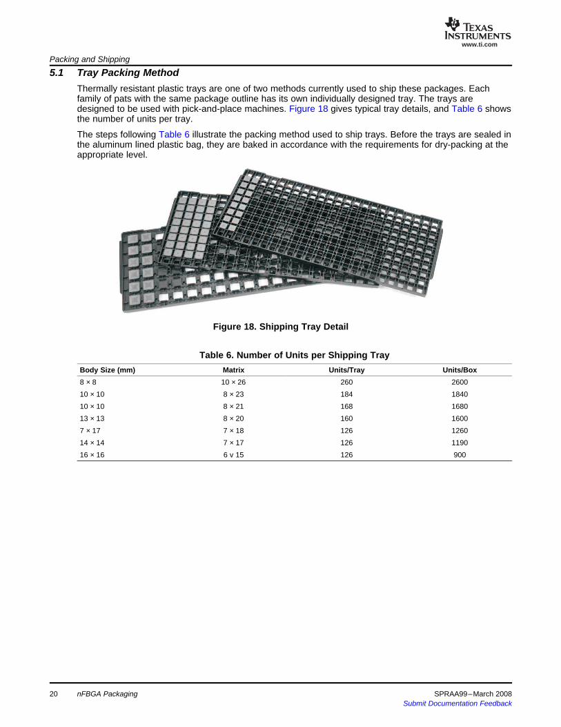
Thermally resistant plastic trays are one of two methods currently used to ship these packages. Eachfamily of pats with the same package outline has its own individually designed tray. The trays aredesigned to be used with pick-and-place machines. Figure 18 gives typical tray details, and Table 6 showsthe number of units per tray.
The steps following Table 6 illustrate the packing method used to ship trays. Before the trays are sealed inthe aluminum lined plastic bag, they are baked in accordance with the requirements for dry-packing at theappropriate level.
Figure 18. Shipping Tray Detail
Table 6. Number of Units per Shipping TrayBody Size (mm) Matrix Units/Tray Units/Box8 × 8 10 × 26 260 260010 × 10 8 × 23 184 184010 × 10 8 × 21 168 168013 × 13 8 × 20 160 16007 × 17 7 × 18 126 126014 × 14 7 × 17 126 119016 × 16 6 v 15 126 900
nFBGA Packaging20 SPRAA99–March 2008Submit Documentation Feedback

www.ti.com
Tray
pad
Tray
stack
Tray
pad
Desiccantpacks
Humidityindicator
Packing and Shipping
1. Arrange the stack of trays to be packed with a tray pad on the top and bottom.
2. Strap the tray stack and pads together with four straps—three crosswise and one lengthwise. Then,place the desiccants and the humidity indicator on top.
SPRAA99–March 2008 nFBGA Packaging 21Submit Documentation Feedback

www.ti.com
Aluminum-linedbag
Moisture-sensitivity label
ESD lable
Bar-code lable
Bar-code lable
ESD lable
Packing and Shipping
3. Place the lot inside the aluminum-lined bag and vacuum-seal it. Place the necessary labels on thesealed bag
4. Wrap and tap bubble pack around the bag for a snug fit in the inner carton. Place the necessary labelson the inner carton.
22 nFBGA Packaging SPRAA99–March 2008Submit Documentation Feedback
www.ti.com
5.2 Tape-and-Reel Packing Method
Packing and Shipping
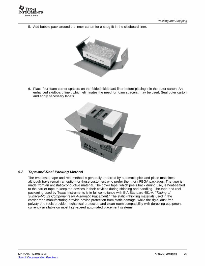
5. Add bubble pack around the inner carton for a snug fit in the skidboard liner.
6. Place four foam corner spacers on the folded skidboard liner before placing it in the outer carton. Anenhanced skidboard liner, which eliminates the need for foam spacers, may be used. Seal outer cartonand apply necessary labels.
The embossed tape-and-reel method is generally preferred by automatic pick-and-place machines,although trays remain an option for those customers who prefer them for nFBGA packages. The tape ismade from an antistatic/conductive material. The cover tape, which peels back during use, is heat-sealedto the carrier tape to keep the devices in their cavities during shipping and handling. The tape-and-reelpackaging used by Texas Instruments is in full compliance with EIA Standard 481-A, “Taping ofSurface-Mount Components for Automatic Placement.” The static-inhibiting materials used in thecarrier-tape manufacturing provide device protection from static damage, while the rigid, dust-freepolystyrene reels provide mechanical protection and clean-room compatibility with dereeling equipmentcurrently available on most high-speed automated placement systems.
SPRAA99–March 2008 nFBGA Packaging 23Submit Documentation Feedback
www.ti.com
5.3 Tape Format
B0
P
4.0 ± 0.10
2.00 ± 0.050.8 MIN
K
0.40
F
W
0 MINK0
Covertape
Carrier tapeembossment
1.5 MINDiameter
A0
Direction
of feed
1.5+ 0.1- 0.0
Packing and Shipping
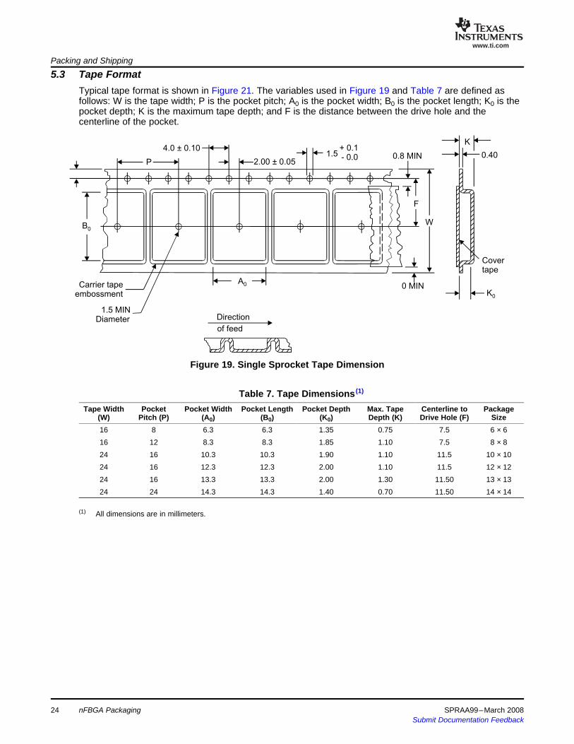
Typical tape format is shown in Figure 21. The variables used in Figure 19 and Table 7 are defined asfollows: W is the tape width; P is the pocket pitch; A0 is the pocket width; B0 is the pocket length; K0 is thepocket depth; K is the maximum tape depth; and F is the distance between the drive hole and thecenterline of the pocket.
Figure 19. Single Sprocket Tape Dimension
Table 7. Tape Dimensions (1)
Tape Width Pocket Pocket Width Pocket Length Pocket Depth Max. Tape Centerline to Package(W) Pitch (P) (A0) (B0) (K0) Depth (K) Drive Hole (F) Size16 8 6.3 6.3 1.35 0.75 7.5 6 × 616 12 8.3 8.3 1.85 1.10 7.5 8 × 824 16 10.3 10.3 1.90 1.10 11.5 10 × 1024 16 12.3 12.3 2.00 1.10 11.5 12 × 1224 16 13.3 13.3 2.00 1.30 11.50 13 × 1324 24 14.3 14.3 1.40 0.70 11.50 14 × 14
(1) All dimensions are in millimeters.
nFBGA Packaging24 SPRAA99–March 2008Submit Documentation Feedback

www.ti.com
330+ 0.0- 4.0
20.2 MIN
2.5 MIN
TI bar code label1.5 MIN width
T MAX
N
13.0 ± 0.2
G
Desiccant
Humidityindicator
Reeled units
Aluminumbag
Pizza box
2D Label
Packing and Shipping
The reels are shown in Figure 20. In this figure, G is the width of the tape, N is the diameter of the hub,and T is the total reel thickness.
Figure 20. Reel Dimensions
Table 8. Reel Dimensions (1)
Tape Width (G) Reel Hub Diameter (N) Reel Total Thickness Parts per Reel(T MAX)
16 100 16.4 250024 100 24.4 1000
(1) After the parts are loaded into the reel, each individual reel is packed in its own “pizza” box for shipping, as shown in Figure 21.
After the parts are loaded into the reel, each individual reel is packed in its own “pizza” box for shipping,as shown in Figure 21.
Figure 21. Tape-and-Reel Packing
SPRAA99–March 2008 nFBGA Packaging 25Submit Documentation Feedback

www.ti.com
5.4 Device Insertion
5.5 Packaging Method
6 Sockets
6.1 The Design Challenge
6.2 Contacting the Ball
Sockets
Devices are inserted toward the outer periphery of the tape by placing the side with the device name faceup and the side with the balls attached face down. The pin-1 indicator is placed in the top left-hand cornerof the pocket, next to the sprocket holes.
For reels, once the taping has been completed, the end of the leader is fixed onto the reel with tape. Theproduct name, lot number, quantity, and date code are recorded on the reel and the cardboard box usedfor tape delivery. Each reel is separately packed in a cardboard box for delivery.
Trays are packed with five loaded trays and one empty tray on top for support and to keep packagessecure. The stack is secured with stable plastic straps and sealed in a moisture-proof bag.
Customer-specific bar code labels can be added under request or general purchasing specification.
Moisture-sensitive packages are baked before packing and are packed within 8 hours of coming out of theoven. Both the tape-and-reel and the tray moisture-proof bags are sealed and marked with appropriatelabeling warning that the packages inside the bags are dry-packed and giving the level of moisturesensitivity.
The fine pitch of nFBGA packages makes socketing a special challenge. Mechanical, thermal, andelectrical issues must be accommodated by the socket designer. The size of a specific package within theTI nFBGA family is based on the package construction, and is independent of die size. Therefore, a rangeof die sizes and I/Os within a family will have the same package dimensions. Each different family has aspecific I/O pitch and array. For maximum socket versatility, an adapter or “personalizer” can becustomized for each application, allowing a single-socket body to be used with many packages. Thisfeature is especially useful in the early days as the technology is being developed and adopted as well asduring volume production phase to minimize socket costs.
A number of different approaches for contacting the solder ball are shown schematically in Figure 22. Thepinch style contact has been used extensively for contacting solder balls in conventional BGAs and isstarting to be proposed also for the most advanced fine pitch CSP packages.
The most common methods used for contacting as small as 0.4 mm pitch CSP packages are either metalpinch (a) or metal (f). Both methods provide the most reliable solutions with less ball deformation andsmall socket form factor at an affordable cost. Texas Instruments Interconnect Business Unit (TI IBU) hasdesigned both pinch and micro tuning fork (metal type) contacts that satisfy all of these requirements.Further information on the availability of these sockets can be obtained from your local TI Field Salesrepresentative.
26 nFBGA Packaging SPRAA99–March 2008Submit Documentation Feedback

www.ti.com
a) Metal pinch b) Metal “Y”
c) Rough bump on flex d) Conductive
e) Etched pocket in silicon f) Metal
Sockets
Figure 22. Approaches for Contacting the Solder Ball
SPRAA99–March 2008 nFBGA Packaging 27Submit Documentation Feedback

www.ti.com
6.3 Pinch ContactSockets
The contact is designed to grip the solder ball with a pinching action. This not only provides electricalcontact to the solder ball but also helps retain the package in the socket. The contact is shown inFigure 23. It was made using a beryllium copper alloy. This alloy is used for spring applications that areexposed to high stresses and temperatures because of its excellent stress relaxation performance andformability.
Figure 23. Pinch Contact for Solder Ball
28 nFBGA Packaging SPRAA99–March 2008Submit Documentation Feedback

www.ti.com
Sockets
Each contact incorporates two beams that provide an oxide-piercing interface with the sides of the ballsabove the central area—the equator. No contact is made on the bottom of the solder ball so the originalpackage planarity specifications are unchanged. A photo-micrograph of the contact touching the solderballs is shown in Figure 24.
Figure 24. Contact Area on Solder Ball
SPRAA99–March 2008 nFBGA Packaging 29Submit Documentation Feedback

www.ti.com
Sockets
The witness marks left on the solder ball from the contact are shown in Figure 25. This ball was contactedat room temperature and it is clear that there was no damage to the bottom of the ball or any witnessmarks from the contact above the equator.
Figure 25. Witness Marks on Solder Ball
30 nFBGA Packaging SPRAA99–March 2008Submit Documentation Feedback
www.ti.com
6.4 Micro Tuning Fork Contact
Sockets
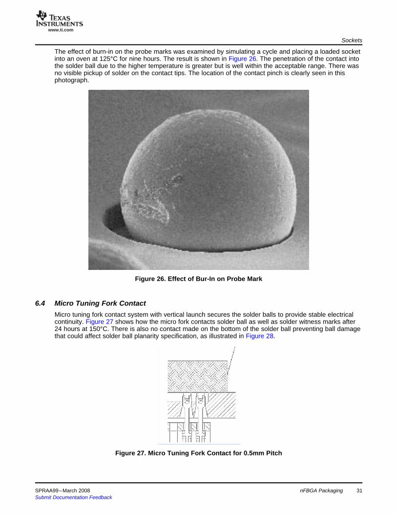
The effect of burn-in on the probe marks was examined by simulating a cycle and placing a loaded socketinto an oven at 125°C for nine hours. The result is shown in Figure 26. The penetration of the contact intothe solder ball due to the higher temperature is greater but is well within the acceptable range. There wasno visible pickup of solder on the contact tips. The location of the contact pinch is clearly seen in thisphotograph.
Figure 26. Effect of Bur-In on Probe Mark
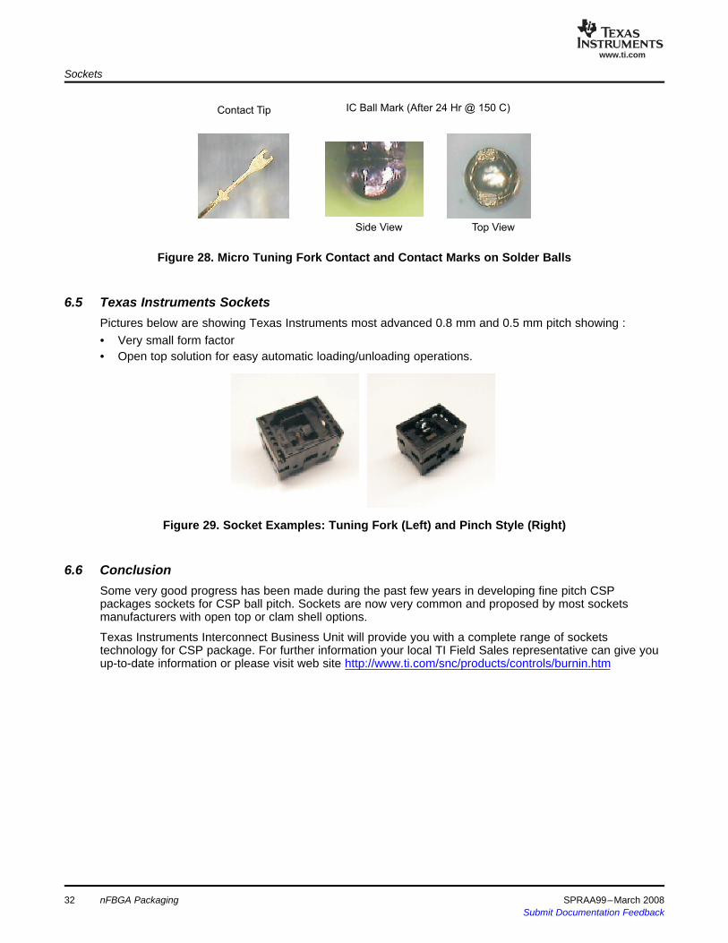
Micro tuning fork contact system with vertical launch secures the solder balls to provide stable electricalcontinuity. Figure 27 shows how the micro fork contacts solder ball as well as solder witness marks after24 hours at 150°C. There is also no contact made on the bottom of the solder ball preventing ball damagethat could affect solder ball planarity specification, as illustrated in Figure 28.
Figure 27. Micro Tuning Fork Contact for 0.5mm Pitch
SPRAA99–March 2008 nFBGA Packaging 31Submit Documentation Feedback
www.ti.com
Contact Tip IC Ball Mark (After 24 Hr @ 150 C)
Side View Top View
6.5 Texas Instruments Sockets
6.6 Conclusion
Sockets
Figure 28. Micro Tuning Fork Contact and Contact Marks on Solder Balls
Pictures below are showing Texas Instruments most advanced 0.8 mm and 0.5 mm pitch showing :• Very small form factor• Open top solution for easy automatic loading/unloading operations.
Figure 29. Socket Examples: Tuning Fork (Left) and Pinch Style (Right)
Some very good progress has been made during the past few years in developing fine pitch CSPpackages sockets for CSP ball pitch. Sockets are now very common and proposed by most socketsmanufacturers with open top or clam shell options.
Texas Instruments Interconnect Business Unit will provide you with a complete range of socketstechnology for CSP package. For further information your local TI Field Sales representative can give youup-to-date information or please visit web site http://www.ti.com/snc/products/controls/burnin.htm
32 nFBGA Packaging SPRAA99–March 2008Submit Documentation Feedback

www.ti.com
Appendix A Frequently Asked Questions
A.1 Package Questions
Appendix A
Q Do the solder balls come off during shipping?A No, this has never been observed. The balls are inspected for coplanarity, diameter, and other
physical properties prior to packing for shipment. Because solder is used during theball-attachment process, uniformly high ball-attachment strengths are developed. Also, theball-attachment strength is monitored frequently in the assembly process to prevent ball loss fromvibration and other shipping forces.
Q Is package repair possible? Are tools available?A Yes, some limited package repair is possible, and there are some semiautomatic M/C tools
available. However, TI does not specify the reliability of repaired packages.Q What are the leads that appear on the package edge for? Are they connected to the inner
pattern?A Those leads are used for plating connections during the plating of Ni/Au on the copper trace
during the fabrication of the substrate. Since they do have electrical connection with the innerpattern, they can be used for test probing and signal analysis. There is no reliability risk withthem.
Q Is burn-in testing possible? How about ball damage?A There are commercial sockets available for fine pitch package burn-in. For further information
your local TI Field Sales representative can give you up-to-date information. The ball damageobserved falls within specified tolerances, so the testing does not affect board mount.
Q Is tape-and-reel shipping available?A Yes, tape-and-reel is an available method for shipping nFBGA packages.Q How does the packaging cost compare to QFPs?A CSPs are in many ways an ideal solution to cost reduction and miniaturization requirements.
They offer enormous area reductions in comparison to QFPs and have increasing potential to doso without adding to system-level costs. In the best case, CSPs compete today on acost-per-terminal basis with QFPs. For example, various CSPs from Texas Instruments are nowavailable at cost parity within QFPs.
SPRAA99–March 2008 33Submit Documentation Feedback

www.ti.com
A.2 Assembly QuestionsAssembly Questions
Q What alignment accuracy is possible?A Alignment accuracy for the nFBGA package is dependent upon board-level pad tolerance,
placement accuracy, and solder ball position tolerance. Nominal ball position tolerances arespecified at ±50 µm. These packages are self-aligning during solder reflow, so final alignmentaccuracy may be better than placement accuracy.
Q Can the solder joints be inspected after reflow?A Process yields of 5-ppm (parts per million) rejects are typically seen, so no final in-line inspection
is required. Some customers are achieving satisfactory results during process set-up withlamographic X-ray techniques.
Q How do the board assembly yields of nFBGAs compare to QFPs?A Many customers are initially concerned about assembly yields. However, once they had nFBGA
packages in production, most of them report improved process yields compared to QFPs. This isdue to the elimination of bent and misoriented leads, and the ability of these packages toself-align during reflow. The collapsing solder balls also mean that the coplanarity is improvedover leaded components.
Q Are there specific recommendations for SMT processing?A Texas Instruments recommends alignment with the solder balls for the CSP package, although it
is possible to use the package outline for alignment. Most customers have found they do notneed to change their reflow profile.
Q Can the boards be repaired?A Yes, there are rework and repair tools and profiles available. TI strongly recommends that
removed packages be discarded.Q What size land diameter for these packages should I design on my board?A Land size is the key to board-level reliability, and Texas Instruments strongly recommends
following the design rules included in this document.
nFBGA Packaging34 SPRAA99–March 2008Submit Documentation Feedback

www.ti.com
Appendix B Package Data Sheets
Appendix B
Table B-1 shows TI’s strategic package lineup, followed by package data sheets for many of thepackage families offered as standard products by Texas Instruments. As new packages are added,they will be placed on the strategic package lineup. Contact your TI field sales office for informationon the most current offerings. Samples are available for all packages shown in Table B-1.
Table B-1. TI’s Strategic Package Line-UpnFBGA Package Product Guide
Pitch Package Size (mm)(mm)
6×6 7×7 8×8 10×10 12×12 13×13 14×14 16×16
0.8 145ZWS 361ZWT
0.65 113ZVD
SPRAA99–March 2008 35Submit Documentation Feedback

www.ti.com
Appendix B
Table B-1. TI’s Strategic Package Line-Up (continued)nFBGA Package Product Guide
0.5 87ZVW 72ZST 195ZWV 225ZWF 289ZVL 289ZWE 447ZAC
143ZWU 241ZWG 293ZVL 447ZAF
143ZZC 318ZVL
152ZZB 325ZVL
385ZWK
385ZWM
36 nFBGA Packaging SPRAA99–March 2008Submit Documentation Feedback

www.ti.com
Appendix B
Table B-1. TI’s Strategic Package Line-Up (continued)nFBGA Package Product Guide
0.4 209ZXN 241ZWJ
289ZWJ
360ZWJ
Figure B-1. 87ZVW Package Outline (6 x 6mm, 0.5mm pitch)
87ZVW Daisy Chain Net List Not Available
SPRAA99–March 2008 nFBGA Packaging 37Submit Documentation Feedback

www.ti.com
Appendix B
Figure B-2. 72ZST Package Outline (7 x 7mm, 0.5mm pitch)
72ZST Daisy Chain Net List Not Available
38 nFBGA Packaging SPRAA99–March 2008Submit Documentation Feedback

www.ti.com
Appendix B
Figure B-3. 143ZZC Package Outline (7 x 7mm, 0.5mm pitch)
143ZZC Daisy Chain Net List Not Available
SPRAA99–March 2008 nFBGA Packaging 39Submit Documentation Feedback

www.ti.com
Appendix B
Figure B-4. 143ZWU Package Outline (7 x 7mm, 0.5mm pitch)
Figure B-5. 143ZWU Daisy Chain Net List
40 nFBGA Packaging SPRAA99–March 2008Submit Documentation Feedback

www.ti.com
Appendix B
Figure B-6. 152ZZB Package Outline (7 x 7mm, 0.5mm pitch)
152ZZB Daisy Chain Net List Not Available
SPRAA99–March 2008 nFBGA Packaging 41Submit Documentation Feedback

www.ti.com
Appendix B
Figure B-7. 209ZXN Package Outline (7 x 7mm, 0.4mm pitch)
209ZXN Daisy Chain Net List Not Available
42 nFBGA Packaging SPRAA99–March 2008Submit Documentation Feedback
www.ti.com
Appendix B
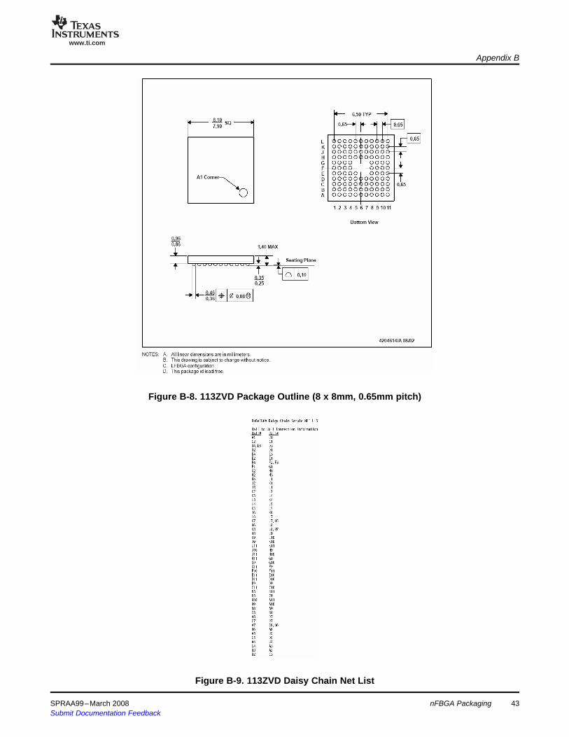
Figure B-8. 113ZVD Package Outline (8 x 8mm, 0.65mm pitch)
Figure B-9. 113ZVD Daisy Chain Net List
SPRAA99–March 2008 nFBGA Packaging 43Submit Documentation Feedback

www.ti.com
Appendix B
Figure B-10. 195ZWV Package Outline (8 x 8mm, 0.5mm pitch)
Figure B-11. 195ZWV Daisy Chain Net List
44 nFBGA Packaging SPRAA99–March 2008Submit Documentation Feedback

www.ti.com
Appendix B
Figure B-12. 225ZWF Package Outline (10 x 10mm, 0.5mm pitch)
225ZWF Daisy Chain Net List Not Available
SPRAA99–March 2008 nFBGA Packaging 45Submit Documentation Feedback

www.ti.com
Appendix B
Figure B-13. 241ZWG Package Outline (10 x 10mm, 0.5mm pitch)
241ZWG Daisy Chain Net List Not Available
46 nFBGA Packaging SPRAA99–March 2008Submit Documentation Feedback

www.ti.com
Appendix B
Figure B-14. 241ZWJ Package Outline (10x10mm, 0.4mm pitch)
Figure B-15. 241ZWJ Daisy Chain Net List
SPRAA99–March 2008 nFBGA Packaging 47Submit Documentation Feedback

www.ti.com
Appendix B
Figure B-16. 289ZWJ Package Outline (10 x 10mm, 0.4mm pitch)
48 nFBGA Packaging SPRAA99–March 2008Submit Documentation Feedback

www.ti.com
Appendix B
Figure B-17. 289ZWJ Daisy Chain Net List
SPRAA99–March 2008 nFBGA Packaging 49Submit Documentation Feedback
www.ti.com
Appendix B
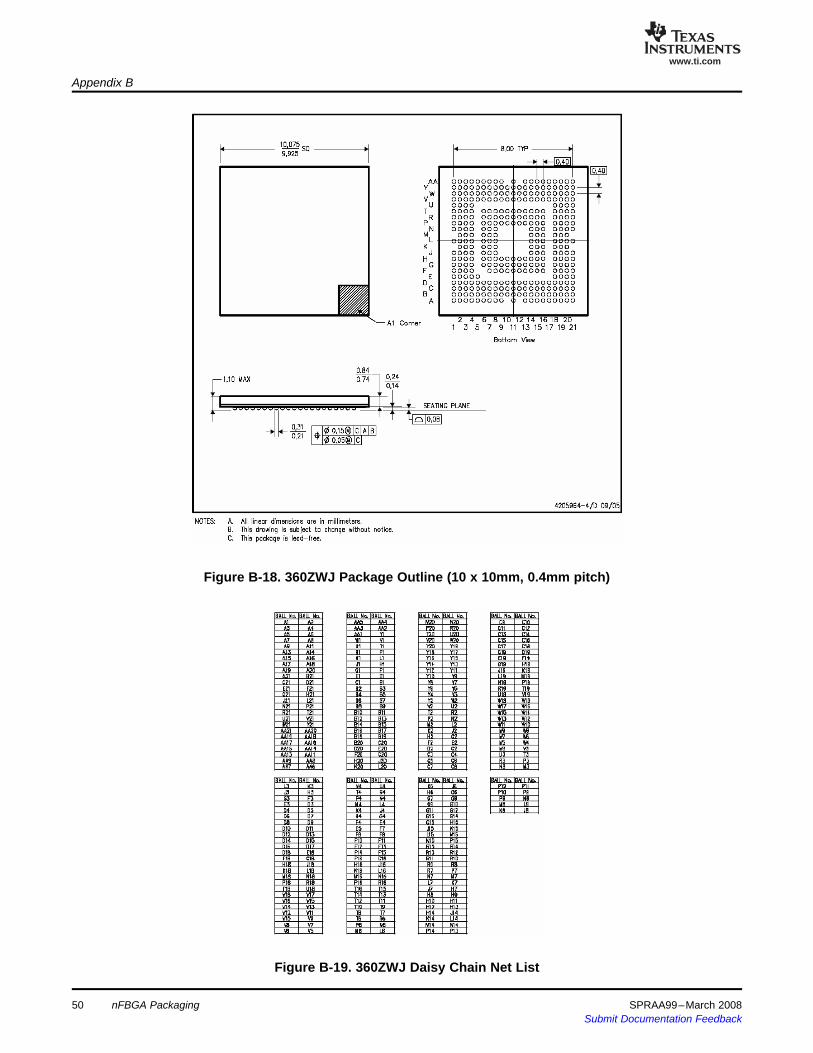
Figure B-18. 360ZWJ Package Outline (10 x 10mm, 0.4mm pitch)
Figure B-19. 360ZWJ Daisy Chain Net List
50 nFBGA Packaging SPRAA99–March 2008Submit Documentation Feedback

www.ti.com
Appendix B
Figure B-20. 145ZWS Package Outline (12 x 12mm, 0.8mm pitch)
145ZWS Daisy Chain Net List Not Available
SPRAA99–March 2008 nFBGA Packaging 51Submit Documentation Feedback

www.ti.com
Appendix B
Figure B-21. 289ZVL Package Outline (12 x 12mm, 0.5mm pitch)
289ZVL Daisy Chain Net List Not Available
52 nFBGA Packaging SPRAA99–March 2008Submit Documentation Feedback

www.ti.com
Appendix B
Figure B-22. 293ZVL Package Outline (12 x 12mm, 0.5mm pitch)
293ZVL Daisy Chain Net List Not Available
SPRAA99–March 2008 nFBGA Packaging 53Submit Documentation Feedback

www.ti.com
Appendix B
Figure B-23. 318ZVL Package Outline (12 x 12mm, 0.5mm pitch)
318ZVL Daisy Chain Net List Not Available
54 nFBGA Packaging SPRAA99–March 2008Submit Documentation Feedback
www.ti.com
Appendix B
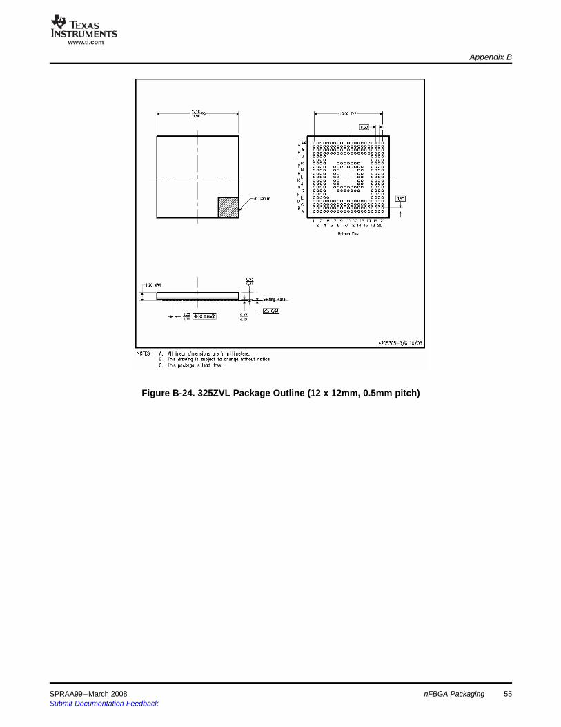
Figure B-24. 325ZVL Package Outline (12 x 12mm, 0.5mm pitch)
SPRAA99–March 2008 nFBGA Packaging 55Submit Documentation Feedback

www.ti.com
Appendix B
Figure B-25. 325ZVL Daisy Chain Net List
56 nFBGA Packaging SPRAA99–March 2008Submit Documentation Feedback

www.ti.com
Appendix B
Figure B-26. 385ZWM Package Outline (12 x 12mm, 0.5mm pitch)
385ZWM Daisy Chain Net List Not Available
SPRAA99–March 2008 nFBGA Packaging 57Submit Documentation Feedback

www.ti.com
Appendix B
Figure B-27. 385ZWK Package Outline (12 x 12mm, 0.5mm pitch)
Figure B-28. 385ZWK Daisy Chain Net List
58 nFBGA Packaging SPRAA99–March 2008Submit Documentation Feedback

www.ti.com
Appendix B
Figure B-29. 289ZWE Package Outline (13 x 13mm, 0.5mm pitch)
289ZWE Daisy Chain Net List Not Available
SPRAA99–March 2008 nFBGA Packaging 59Submit Documentation Feedback

www.ti.com
Appendix B
Figure B-30. 447ZAC Package Outline (14 x 14mm, 0.5mm pitch)
447ZAC Daisy Chain Net List Not Available
60 nFBGA Packaging SPRAA99–March 2008Submit Documentation Feedback

www.ti.com
Appendix B
Figure B-31. 447ZAF Package Outline (14 x 14mm, 0.5mm pitch)
447ZAF Daisy Chain Net List Not Available
SPRAA99–March 2008 nFBGA Packaging 61Submit Documentation Feedback

www.ti.com
Appendix B
Figure B-32. 361ZWT Package Outline (16 x 16mm, 0.8mm pitch)
Figure B-33. 361ZWT Daisy Chain Net List
62 nFBGA Packaging SPRAA99–March 2008Submit Documentation Feedback

www.ti.com
Appendix B
SPRAA99–March 2008 nFBGA Packaging 63Submit Documentation Feedback
www.ti.com
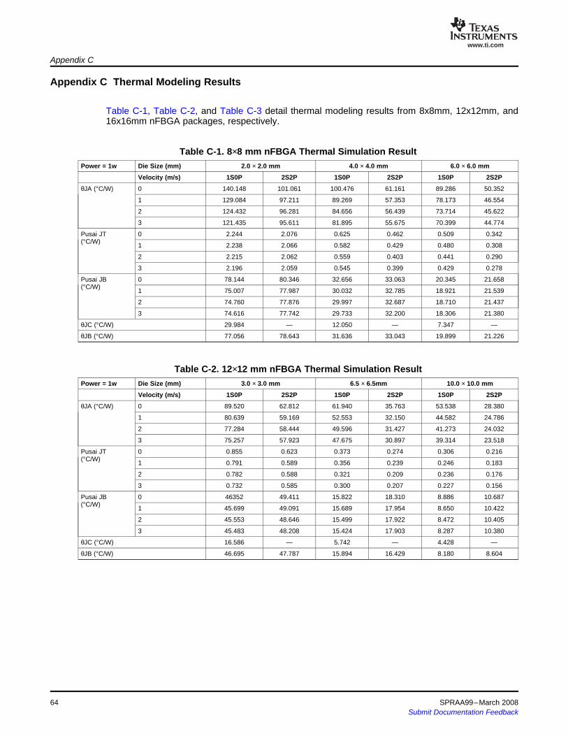
Appendix C Thermal Modeling Results
Appendix C
Table C-1, Table C-2, and Table C-3 detail thermal modeling results from 8x8mm, 12x12mm, and16x16mm nFBGA packages, respectively.
Table C-1. 8×8 mm nFBGA Thermal Simulation ResultPower = 1w Die Size (mm) 2.0 × 2.0 mm 4.0 × 4.0 mm 6.0 × 6.0 mm
Velocity (m/s) 1S0P 2S2P 1S0P 2S2P 1S0P 2S2P
θJA (°C/W) 0 140.148 101.061 100.476 61.161 89.286 50.352
1 129.084 97.211 89.269 57.353 78.173 46.554
2 124.432 96.281 84.656 56.439 73.714 45.622
3 121.435 95.611 81.895 55.675 70.399 44.774
Pusai JT 0 2.244 2.076 0.625 0.462 0.509 0.342(°C/W) 1 2.238 2.066 0.582 0.429 0.480 0.308
2 2.215 2.062 0.559 0.403 0.441 0.290
3 2.196 2.059 0.545 0.399 0.429 0.278
Pusai JB 0 78.144 80.346 32.656 33.063 20.345 21.658(°C/W) 1 75.007 77.987 30.032 32.785 18.921 21.539
2 74.760 77.876 29.997 32.687 18.710 21.437
3 74.616 77.742 29.733 32.200 18.306 21.380
θJC (°C/W) 29.984 — 12.050 — 7.347 —
θJB (°C/W) 77.056 78.643 31.636 33.043 19.899 21.226
Table C-2. 12×12 mm nFBGA Thermal Simulation ResultPower = 1w Die Size (mm) 3.0 × 3.0 mm 6.5 × 6.5mm 10.0 × 10.0 mm
Velocity (m/s) 1S0P 2S2P 1S0P 2S2P 1S0P 2S2P
θJA (°C/W) 0 89.520 62.812 61.940 35.763 53.538 28.380
1 80.639 59.169 52.553 32.150 44.582 24.786
2 77.284 58.444 49.596 31.427 41.273 24.032
3 75.257 57.923 47.675 30.897 39.314 23.518
Pusai JT 0 0.855 0.623 0.373 0.274 0.306 0.216(°C/W) 1 0.791 0.589 0.356 0.239 0.246 0.183
2 0.782 0.588 0.321 0.209 0.236 0.176
3 0.732 0.585 0.300 0.207 0.227 0.156
Pusai JB 0 46352 49.411 15.822 18.310 8.886 10.687(°C/W) 1 45.699 49.091 15.689 17.954 8.650 10.422
2 45.553 48.646 15.499 17.922 8.472 10.405
3 45.483 48.208 15.424 17.903 8.287 10.380
θJC (°C/W) 16.586 — 5.742 — 4.428 —
θJB (°C/W) 46.695 47.787 15.894 16.429 8.180 8.604
64 SPRAA99–March 2008Submit Documentation Feedback

www.ti.com
Appendix C
Table C-3. 16×16 mm nFBGA Thermal Simulation ResultPower = 1w Die Size (mm) 3.0 × 3.0 mm 8.5 × 8.5mm 14.0 × 14.0 mm
Velocity (m/s) 1S0P 2S2P 1S0P 2S2P 1S0P 2S2P
θJA (°C/W) 0 88.870 69.542 48.861 27.847 39.056 21.145
1 81.509 66.538 69.164 24.125 31.690 17.579
2 79.283 65.851 36.777 23.404 28.913 16.870
3 77.860 65.395 35.387 22.974 27.514 16.410
Pusai JT 0 0.888 0.820 0.290 0.355 0.237 0.181(°C/W) 1 0.828 0.755 0.226 0.280 0.177 0.103
2 0.808 0.740 0.225 0.155 0.164 0.099
3 0.801 0.737 0.218 0.153 0.159 0.098
Pusai JB 0 59.993 61.429 11.901 12.620 5.252 5.523(°C/W) 1 59.895 61.026 11.667 11.925 5.231 5.470
2 59.349 59.877 11.270 11.591 4.806 5.267
3 59.284 59.842 11.176 11.584 4.776 5.104
θJC (°C/W) 20.002 — 3.797 — 1.853 —
θJB (°C/W) 57.658 58.886 10.183 10.717 4.898 5.158
SPRAA99–March 2008 nFBGA Packaging 65Submit Documentation Feedback

IMPORTANT NOTICETexas Instruments Incorporated and its subsidiaries (TI) reserve the right to make corrections, modifications, enhancements, improvements,and other changes to its products and services at any time and to discontinue any product or service without notice. Customers shouldobtain the latest relevant information before placing orders and should verify that such information is current and complete. All products aresold subject to TI’s terms and conditions of sale supplied at the time of order acknowledgment.TI warrants performance of its hardware products to the specifications applicable at the time of sale in accordance with TI’s standardwarranty. Testing and other quality control techniques are used to the extent TI deems necessary to support this warranty. Except wheremandated by government requirements, testing of all parameters of each product is not necessarily performed.TI assumes no liability for applications assistance or customer product design. Customers are responsible for their products andapplications using TI components. To minimize the risks associated with customer products and applications, customers should provideadequate design and operating safeguards.TI does not warrant or represent that any license, either express or implied, is granted under any TI patent right, copyright, mask work right,or other TI intellectual property right relating to any combination, machine, or process in which TI products or services are used. Informationpublished by TI regarding third-party products or services does not constitute a license from TI to use such products or services or awarranty or endorsement thereof. Use of such information may require a license from a third party under the patents or other intellectualproperty of the third party, or a license from TI under the patents or other intellectual property of TI.Reproduction of TI information in TI data books or data sheets is permissible only if reproduction is without alteration and is accompaniedby all associated warranties, conditions, limitations, and notices. Reproduction of this information with alteration is an unfair and deceptivebusiness practice. TI is not responsible or liable for such altered documentation. Information of third parties may be subject to additionalrestrictions.Resale of TI products or services with statements different from or beyond the parameters stated by TI for that product or service voids allexpress and any implied warranties for the associated TI product or service and is an unfair and deceptive business practice. TI is notresponsible or liable for any such statements.TI products are not authorized for use in safety-critical applications (such as life support) where a failure of the TI product would reasonablybe expected to cause severe personal injury or death, unless officers of the parties have executed an agreement specifically governingsuch use. Buyers represent that they have all necessary expertise in the safety and regulatory ramifications of their applications, andacknowledge and agree that they are solely responsible for all legal, regulatory and safety-related requirements concerning their productsand any use of TI products in such safety-critical applications, notwithstanding any applications-related information or support that may beprovided by TI. Further, Buyers must fully indemnify TI and its representatives against any damages arising out of the use of TI products insuch safety-critical applications.TI products are neither designed nor intended for use in military/aerospace applications or environments unless the TI products arespecifically designated by TI as military-grade or "enhanced plastic." Only products designated by TI as military-grade meet militaryspecifications. Buyers acknowledge and agree that any such use of TI products which TI has not designated as military-grade is solely atthe Buyer's risk, and that they are solely responsible for compliance with all legal and regulatory requirements in connection with such use.TI products are neither designed nor intended for use in automotive applications or environments unless the specific TI products aredesignated by TI as compliant with ISO/TS 16949 requirements. Buyers acknowledge and agree that, if they use any non-designatedproducts in automotive applications, TI will not be responsible for any failure to meet such requirements.Following are URLs where you can obtain information on other Texas Instruments products and application solutions:Products ApplicationsAmplifiers amplifier.ti.com Audio www.ti.com/audioData Converters dataconverter.ti.com Automotive www.ti.com/automotiveDSP dsp.ti.com Broadband www.ti.com/broadbandClocks and Timers www.ti.com/clocks Digital Control www.ti.com/digitalcontrolInterface interface.ti.com Medical www.ti.com/medicalLogic logic.ti.com Military www.ti.com/militaryPower Mgmt power.ti.com Optical Networking www.ti.com/opticalnetworkMicrocontrollers microcontroller.ti.com Security www.ti.com/securityRFID www.ti-rfid.com Telephony www.ti.com/telephonyRF/IF and ZigBee® Solutions www.ti.com/lprf Video & Imaging www.ti.com/video
Wireless www.ti.com/wireless
Mailing Address: Texas Instruments, Post Office Box 655303, Dallas, Texas 75265Copyright © 2008, Texas Instruments Incorporated