Embed Size (px)
Citation preview

TMS320C6748 DSPSystem
Reference Guide
Literature Number: SPRUGJ7D
April 2010

2 SPRUGJ7D–April 2010
Copyright © 2010, Texas Instruments Incorporated

Contents
Preface ...................................................................................................................................... 15
1 Overview .......................................................................................................................... 171.1 Introduction ................................................................................................................. 181.2 Block Diagram ............................................................................................................. 181.3 DSP Subsystem ........................................................................................................... 18
2 DSP Subsystem ................................................................................................................ 192.1 Introduction ................................................................................................................. 202.2 TMS320C674x Megamodule ............................................................................................. 21
2.2.1 Internal Memory Controllers ..................................................................................... 212.2.2 Internal Peripherals ............................................................................................... 21
2.3 Memory Map ............................................................................................................... 262.3.1 DSP Internal Memory ............................................................................................ 262.3.2 External Memory .................................................................................................. 26
2.4 Advanced Event Triggering (AET) ...................................................................................... 26
3 System Interconnect .......................................................................................................... 273.1 Introduction ................................................................................................................. 283.2 System Interconnect Block Diagram .................................................................................... 29
4 System Memory ................................................................................................................ 314.1 Introduction ................................................................................................................. 324.2 DSP Memories ............................................................................................................. 324.3 Shared RAM Memory ..................................................................................................... 324.4 External Memories ........................................................................................................ 324.5 Internal Peripherals ........................................................................................................ 334.6 Peripherals ................................................................................................................. 33
5 Memory Protection Unit (MPU) ............................................................................................ 355.1 Introduction ................................................................................................................. 36
5.1.1 Purpose of the MPU ............................................................................................. 365.1.2 Features ........................................................................................................... 365.1.3 Block Diagram .................................................................................................... 365.1.4 MPU Default Configuration ...................................................................................... 37
5.2 Architecture ................................................................................................................. 375.2.1 Privilege Levels ................................................................................................... 375.2.2 Memory Protection Ranges ..................................................................................... 385.2.3 Permission Structures ............................................................................................ 385.2.4 Protection Check ................................................................................................. 405.2.5 DSP L1/L2 Cache Controller Accesses ....................................................................... 405.2.6 MPU Register Protection ........................................................................................ 405.2.7 Invalid Accesses and Exceptions .............................................................................. 415.2.8 Reset Considerations ............................................................................................ 415.2.9 Interrupt Support .................................................................................................. 415.2.10 Emulation Considerations ...................................................................................... 41
5.3 MPU Registers ............................................................................................................. 425.3.1 Revision Identification Register (REVID) ...................................................................... 445.3.2 Configuration Register (CONFIG) .............................................................................. 44
3SPRUGJ7D–April 2010 Contents
Copyright © 2010, Texas Instruments Incorporated

www.ti.com
5.3.3 Interrupt Raw Status/Set Register (IRAWSTAT) ............................................................. 455.3.4 Interrupt Enable Status/Clear Register (IENSTAT) .......................................................... 465.3.5 Interrupt Enable Set Register (IENSET) ....................................................................... 475.3.6 Interrupt Enable Clear Register (IENCLR) .................................................................... 475.3.7 Fixed Range Start Address Register (FXD_MPSAR) ....................................................... 485.3.8 Fixed Range End Address Register (FXD_MPEAR) ........................................................ 485.3.9 Fixed Range Memory Protection Page Attributes Register (FXD_MPPA) ................................ 495.3.10 Programmable Range n Start Address Registers (PROGn_MPSAR) .................................... 505.3.11 Programmable Range n End Address Registers (PROGn_MPEAR) .................................... 515.3.12 Programmable Range n Memory Protection Page Attributes Register (PROGn_MPPA) ............. 525.3.13 Fault Address Register (FLTADDRR) ........................................................................ 535.3.14 Fault Status Register (FLTSTAT) ............................................................................. 545.3.15 Fault Clear Register (FLTCLR) ................................................................................ 55
6 Device Clocking ................................................................................................................ 576.1 Overview .................................................................................................................... 586.2 Frequency Flexibility ...................................................................................................... 606.3 Peripheral Clocking ........................................................................................................ 61
6.3.1 USB Clocking ..................................................................................................... 616.3.2 DDR2/mDDR Memory Controller Clocking .................................................................... 636.3.3 EMIFA Clocking ................................................................................................... 656.3.4 EMAC Clocking ................................................................................................... 666.3.5 uPP Clocking ...................................................................................................... 686.3.6 McASP Clocking .................................................................................................. 696.3.7 I/O Domains ....................................................................................................... 70
7 Phase-Locked Loop Controller (PLLC) ................................................................................. 717.1 Introduction ................................................................................................................. 727.2 PLL Controllers ............................................................................................................ 72
7.2.1 Device Clock Generation ........................................................................................ 747.2.2 Steps for Programming the PLLs ............................................................................... 75
7.3 PLLC Registers ............................................................................................................ 777.3.1 PLLC0 Revision Identification Register (REVID) ............................................................. 787.3.2 PLLC1 Revision Identification Register (REVID) ............................................................. 797.3.3 Reset Type Status Register (RSTYPE) ....................................................................... 797.3.4 PLLC0 Control Register (PLLCTL) ............................................................................. 807.3.5 PLLC1 Control Register (PLLCTL) ............................................................................. 817.3.6 PLLC0 OBSCLK Select Register (OCSEL) ................................................................... 827.3.7 PLLC1 OBSCLK Select Register (OCSEL) ................................................................... 837.3.8 PLL Multiplier Control Register (PLLM) ........................................................................ 847.3.9 PLLC0 Pre-Divider Control Register (PREDIV) .............................................................. 847.3.10 PLLC0 Divider 1 Register (PLLDIV1) ......................................................................... 857.3.11 PLLC1 Divider 1 Register (PLLDIV1) ......................................................................... 857.3.12 PLLC0 Divider 2 Register (PLLDIV2) ......................................................................... 867.3.13 PLLC1 Divider 2 Register (PLLDIV2) ......................................................................... 867.3.14 PLLC0 Divider 3 Register (PLLDIV3) ......................................................................... 877.3.15 PLLC1 Divider 3 Register (PLLDIV3) ......................................................................... 877.3.16 PLLC0 Divider 4 Register (PLLDIV4) ......................................................................... 887.3.17 PLLC0 Divider 5 Register (PLLDIV5) ......................................................................... 887.3.18 PLLC0 Divider 6 Register (PLLDIV6) ......................................................................... 897.3.19 PLLC0 Divider 7 Register (PLLDIV7) ......................................................................... 897.3.20 PLLC0 Oscillator Divider 1 Register (OSCDIV) ............................................................. 907.3.21 PLLC1 Oscillator Divider 1 Register (OSCDIV) ............................................................. 907.3.22 PLL Post-Divider Control Register (POSTDIV) .............................................................. 917.3.23 PLL Controller Command Register (PLLCMD) .............................................................. 91
4 Contents SPRUGJ7D–April 2010
Copyright © 2010, Texas Instruments Incorporated

www.ti.com
7.3.24 PLL Controller Status Register (PLLSTAT) .................................................................. 927.3.25 PLLC0 Clock Align Control Register (ALNCTL) ............................................................. 937.3.26 PLLC1 Clock Align Control Register (ALNCTL) ............................................................. 947.3.27 PLLC0 PLLDIV Ratio Change Status Register (DCHANGE) .............................................. 957.3.28 PLLC1 PLLDIV Ratio Change Status Register (DCHANGE) .............................................. 967.3.29 PLLC0 Clock Enable Control Register (CKEN) ............................................................. 977.3.30 PLLC0 Clock Status Register (CKSTAT) ..................................................................... 987.3.31 PLLC0 SYSCLK Status Register (SYSTAT) ................................................................. 997.3.32 PLLC1 SYSCLK Status Register (SYSTAT) ............................................................... 1007.3.33 Emulation Performance Counter 0 Register (EMUCNT0) ................................................ 1017.3.34 Emulation Performance Counter 1 Register (EMUCNT1) ................................................ 101
8 Power and Sleep Controller (PSC) ..................................................................................... 1038.1 Introduction ............................................................................................................... 1048.2 Power Domain and Module Topology ................................................................................. 104
8.2.1 Power Domain States .......................................................................................... 1068.2.2 Module States ................................................................................................... 106
8.3 Executing State Transitions ............................................................................................ 1088.3.1 Power Domain State Transitions .............................................................................. 1088.3.2 Module State Transitions ....................................................................................... 108
8.4 IcePick Emulation Support in the PSC ................................................................................ 1098.5 PSC Interrupts ............................................................................................................ 109
8.5.1 Interrupt Events ................................................................................................. 1098.5.2 Interrupt Registers .............................................................................................. 1108.5.3 Interrupt Handling ............................................................................................... 111
8.6 PSC Registers ............................................................................................................ 1128.6.1 Revision Identification Register (REVID) .................................................................... 1138.6.2 Interrupt Evaluation Register (INTEVAL) .................................................................... 1138.6.3 PSC0 Module Error Pending Register 0 (modules 0-15) (MERRPR0) .................................. 1148.6.4 PSC1 Module Error Pending Register 0 (modules 0-31) (MERRPR0) .................................. 1148.6.5 PSC0 Module Error Clear Register 0 (modules 0-15) (MERRCR0) ...................................... 1158.6.6 PSC1 Module Error Clear Register 0 (modules 0-31) (MERRCR0) ...................................... 1158.6.7 Power Error Pending Register (PERRPR) ................................................................... 1168.6.8 Power Error Clear Register (PERRCR) ...................................................................... 1168.6.9 Power Domain Transition Command Register (PTCMD) .................................................. 1178.6.10 Power Domain Transition Status Register (PTSTAT) ..................................................... 1188.6.11 Power Domain 0 Status Register (PDSTAT0) ............................................................. 1198.6.12 Power Domain 1 Status Register (PDSTAT1) ............................................................. 1208.6.13 Power Domain 0 Control Register (PDCTL0) .............................................................. 1218.6.14 Power Domain 1 Control Register (PDCTL1) .............................................................. 1228.6.15 Power Domain 0 Configuration Register (PDCFG0) ...................................................... 1238.6.16 Power Domain 1 Configuration Register (PDCFG1) ...................................................... 1248.6.17 Module Status n Register (MDSTATn) ...................................................................... 1258.6.18 PSC0 Module Control n Register (modules 0-15) (MDCTLn) ............................................ 1268.6.19 PSC1 Module Control n Register (modules 0-31) (MDCTLn) ............................................ 127
9 Power Management .......................................................................................................... 1299.1 Introduction ............................................................................................................... 1309.2 Power Consumption Overview ......................................................................................... 1309.3 PSC and PLLC Overview ............................................................................................... 1309.4 Features ................................................................................................................... 1319.5 Clock Management ...................................................................................................... 132
9.5.1 Module Clock ON/OFF ......................................................................................... 1329.5.2 Module Clock Frequency Scaling ............................................................................. 1329.5.3 PLL Bypass and Power Down ................................................................................. 132
5SPRUGJ7D–April 2010 Contents
Copyright © 2010, Texas Instruments Incorporated
www.ti.com
9.6 DSP Sleep Mode Management ........................................................................................ 1339.6.1 C674x DSP CPU Sleep Mode ................................................................................. 1339.6.2 C674x Megamodule Sleep Mode ............................................................................. 133
9.7 RTC-Only Mode .......................................................................................................... 1339.8 Dynamic Voltage and Frequency Scaling (DVFS) ................................................................... 133
9.8.1 Frequency Scaling Considerations ........................................................................... 1349.8.2 Voltage Scaling Considerations ............................................................................... 135
9.9 Deep Sleep Mode ........................................................................................................ 1359.9.1 Entering/Exiting Deep Sleep Mode Using Externally Controlled Wake-Up .............................. 1359.9.2 Entering/Exiting Deep Sleep Mode Using RTC Controlled Wake-Up .................................... 1369.9.3 Deep Sleep Sequence ......................................................................................... 1379.9.4 Entering/Exiting Deep Sleep Mode Using Software Handshaking ....................................... 137
9.10 Additional Peripheral Power Management Considerations ......................................................... 1389.10.1 USB PHY Power Down Control .............................................................................. 1389.10.2 DDR2/mDDR Memory Controller Clock Gating and Self-Refresh Mode ............................... 1389.10.3 SATA PHY Power Down ...................................................................................... 1399.10.4 LVCMOS I/O Buffer Receiver Disable ...................................................................... 1399.10.5 Pull-Up/Pull-Down Disable .................................................................................... 139
10 System Configuration (SYSCFG) Module ............................................................................ 14110.1 Introduction ............................................................................................................... 14210.2 Protection ................................................................................................................. 142
10.2.1 Privilege Mode Protection ..................................................................................... 14210.2.2 Kicker Mechanism Protection ................................................................................ 143
10.3 Master Priority Control ................................................................................................... 14310.4 Host-DSP Communication Interrupts .................................................................................. 14510.5 SYSCFG Registers ...................................................................................................... 145
10.5.1 Revision Identification Register (REVID) ................................................................... 14710.5.2 Device Identification Register 0 (DEVIDR0) ................................................................ 14710.5.3 Boot Configuration Register (BOOTCFG) .................................................................. 14810.5.4 Kick Registers (KICK0R-KICK1R) ........................................................................... 14910.5.5 Host 1 Configuration Register (HOST1CFG) ............................................................... 15010.5.6 Interrupt Registers ............................................................................................. 15110.5.7 Fault Registers ................................................................................................. 15410.5.8 Master Priority Registers (MSTPRI0-MSTPRI2) ........................................................... 15610.5.9 Pin Multiplexing Control Registers (PINMUX0-PINMUX19) .............................................. 15910.5.10 Suspend Source Register (SUSPSRC) ................................................................... 19910.5.11 Chip Signal Register (CHIPSIG) ........................................................................... 20210.5.12 Chip Signal Clear Register (CHIPSIG_CLR) ............................................................. 20310.5.13 Chip Configuration 0 Register (CFGCHIP0) .............................................................. 20410.5.14 Chip Configuration 1 Register (CFGCHIP1) .............................................................. 20510.5.15 Chip Configuration 2 Register (CFGCHIP2) .............................................................. 20810.5.16 Chip Configuration 3 Register (CFGCHIP3) .............................................................. 21010.5.17 Chip Configuration 4 Register (CFGCHIP4) .............................................................. 21110.5.18 VTP I/O Control Register (VTPIO_CTL) ................................................................... 21210.5.19 DDR Slew Register (DDR_SLEW) ......................................................................... 21410.5.20 Deep Sleep Register (DEEPSLEEP) ...................................................................... 21510.5.21 Pullup/Pulldown Enable Register (PUPD_ENA) ......................................................... 21610.5.22 Pullup/Pulldown Select Register (PUPD_SEL) ........................................................... 21610.5.23 RXACTIVE Control Register (RXACTIVE) ................................................................ 21810.5.24 Power Down Control Register (PWRDN) ................................................................. 218
11 Boot Considerations ........................................................................................................ 21911.1 Introduction ............................................................................................................... 220
A Revision History .............................................................................................................. 221
6 Contents SPRUGJ7D–April 2010
Copyright © 2010, Texas Instruments Incorporated

www.ti.com
List of Figures
1-1. TMS320C6748 DSP Block Diagram .................................................................................... 18
2-1. TMS320C674x Megamodule Block Diagram .......................................................................... 20
3-1. System Interconnect Block Diagram .................................................................................... 29
5-1. MPU Block Diagram....................................................................................................... 36
5-2. Revision ID Register (REVID) ........................................................................................... 44
5-3. Configuration Register (CONFIG) ....................................................................................... 44
5-4. Interrupt Raw Status/Set Register (IRAWSTAT) ...................................................................... 45
5-5. Interrupt Enable Status/Clear Register (IENSTAT) ................................................................... 46
5-6. Interrupt Enable Set Register (IENSET)................................................................................ 47
5-7. Interrupt Enable Clear Register (IENCLR) ............................................................................. 47
5-8. Fixed Range Start Address Register (FXD_MPSAR) ................................................................ 48
5-9. Fixed Range End Address Register (FXD_MPEAR) ................................................................. 48
5-10. Fixed Range Memory Protection Page Attributes Register (FXD_MPPA)......................................... 49
5-11. MPU1 Programmable Range n Start Address Register (PROGn_MPSAR)....................................... 50
5-12. MPU2 Programmable Range n Start Address Register (PROGn_MPSAR)....................................... 50
5-13. MPU1 Programmable Range n End Address Register (PROGn_MPEAR)........................................ 51
5-14. MPU2 Programmable Range n End Address Register (PROGn_MPEAR)........................................ 51
5-15. Programmable Range Memory Protection Page Attributes Register (PROGn_MPPA).......................... 52
5-16. Fault Address Register (FLTADDRR) .................................................................................. 53
5-17. Fault Status Register (FLTSTAT) ....................................................................................... 54
5-18. Fault Clear Register (FLTCLR) .......................................................................................... 55
6-1. Overall Clocking Diagram ................................................................................................ 59
6-2. USB Clocking Diagram ................................................................................................... 62
6-3. DDR2/mDDR Memory Controller Clocking Diagram.................................................................. 64
6-4. EMIFA Clocking Diagram................................................................................................. 65
6-5. EMAC Clocking Diagram ................................................................................................. 66
6-6. uPP Clocking Diagram.................................................................................................... 68
6-7. McASP Clocking Diagram................................................................................................ 69
7-1. PLLC Structure ............................................................................................................ 73
7-2. PLLC0 Revision Identification Register (REVID) ...................................................................... 78
7-3. PLLC1 Revision Identification Register (REVID) ...................................................................... 79
7-4. Reset Type Status Register (RSTYPE) ................................................................................ 79
7-5. PLLC0 Control Register (PLLCTL) ...................................................................................... 80
7-6. PLLC1 Control Register (PLLCTL) ...................................................................................... 81
7-7. PLLC0 OBSCLK Select Register (OCSEL) ............................................................................ 82
7-8. PLLC1 OBSCLK Select Register (OCSEL) ............................................................................ 83
7-9. PLL Multiplier Control Register (PLLM)................................................................................. 84
7-10. PLLC0 Pre-Divider Control Register (PREDIV) ....................................................................... 84
7-11. PLLC0 Divider 1 Register (PLLDIV1) ................................................................................... 85
7-12. PLLC1 Divider 1 Register (PLLDIV1) ................................................................................... 85
7-13. PLLC0 Divider 2 Register (PLLDIV2) .................................................................................. 86
7-14. PLLC1 Divider 2 Register (PLLDIV2) .................................................................................. 86
7-15. PLLC0 Divider 3 Register (PLLDIV3) .................................................................................. 87
7-16. PLLC1 Divider 3 Register (PLLDIV3) .................................................................................. 87
7-17. PLLC0 Divider 4 Register (PLLDIV4) ................................................................................... 88
7-18. PLLC0 Divider 5 Register (PLLDIV5) ................................................................................... 88
7-19. PLLC0 Divider 6 Register (PLLDIV6) ................................................................................... 89
7SPRUGJ7D–April 2010 List of Figures
Copyright © 2010, Texas Instruments Incorporated

www.ti.com
7-20. PLLC0 Divider 7 Register (PLLDIV7) ................................................................................... 89
7-21. PLLC0 Oscillator Divider 1 Register (OSCDIV) ....................................................................... 90
7-22. PLLC1 Oscillator Divider 1 Register (OSCDIV) ....................................................................... 90
7-23. PLL Post-Divider Control Register (POSTDIV) ........................................................................ 91
7-24. PLL Controller Command Register (PLLCMD) ........................................................................ 91
7-25. PLL Controller Status Register (PLLSTAT) ............................................................................ 92
7-26. PLLC0 Clock Align Control Register (ALNCTL) ....................................................................... 93
7-27. PLLC1 Clock Align Control Register (ALNCTL) ....................................................................... 94
7-28. PLLC0 PLLDIV Ratio Change Status Register (DCHANGE) ........................................................ 95
7-29. PLLC1 PLLDIV Ratio Change Status Register (DCHANGE) ........................................................ 96
7-30. PLLC0 Clock Enable Control Register (CKEN) ....................................................................... 97
7-31. PLLC0 Clock Status Register (CKSTAT)............................................................................... 98
7-32. PLLC0 SYSCLK Status Register (SYSTAT) ........................................................................... 99
7-33. PLLC1 SYSCLK Status Register (SYSTAT) ......................................................................... 100
7-34. Emulation Performance Counter 0 Register (EMUCNT0) .......................................................... 101
7-35. Emulation Performance Counter 1 Register (EMUCNT1) .......................................................... 101
8-1. Revision Identification Register (REVID) ............................................................................. 113
8-2. Interrupt Evaluation Register (INTEVAL) ............................................................................. 113
8-3. PSC0 Module Error Pending Register 0 (MERRPR0) .............................................................. 114
8-4. PSC1 Module Error Pending Register 0 (MERRPR0) .............................................................. 114
8-5. PSC0 Module Error Clear Register 0 (MERRCR0).................................................................. 115
8-6. PSC1 Module Error Clear Register 0 (MERRCR0).................................................................. 115
8-7. Power Error Pending Register (PERRPR)............................................................................ 116
8-8. Power Error Clear Register (PERRCR) ............................................................................... 116
8-9. Power Domain Transition Command Register (PTCMD)........................................................... 117
8-10. Power Domain Transition Status Register (PTSTAT)............................................................... 118
8-11. Power Domain 0 Status Register (PDSTAT0) ....................................................................... 119
8-12. Power Domain 1 Status Register (PDSTAT1) ....................................................................... 120
8-13. Power Domain 0 Control Register (PDCTL0) ........................................................................ 121
8-14. Power Domain 1 Control Register (PDCTL1) ........................................................................ 122
8-15. Power Domain 0 Configuration Register (PDCFG0) ................................................................ 123
8-16. Power Domain 1 Configuration Register (PDCFG1) ................................................................ 124
8-17. Module Status n Register (MDSTATn)................................................................................ 125
8-18. PSC0 Module Control n Register (MDCTLn)......................................................................... 126
8-19. PSC1 Module Control n Register (MDCTLn)......................................................................... 127
9-1. Deep Sleep Mode Sequence........................................................................................... 137
10-1. Revision Identification Register (REVID) ............................................................................. 147
10-2. Device Identification Register 0 (DEVIDR0).......................................................................... 147
10-3. Boot Configuration Register (BOOTCFG) ............................................................................ 148
10-4. Kick 0 Register (KICK0R) ............................................................................................... 149
10-5. Kick 1 Register (KICK1R) ............................................................................................... 149
10-6. Host 1 Configuration Register (HOST1CFG)......................................................................... 150
10-7. Interrupt Raw Status/Set Register (IRAWSTAT)..................................................................... 151
10-8. Interrupt Enable Status/Clear Register (IENSTAT).................................................................. 152
10-9. Interrupt Enable Register (IENSET) ................................................................................... 153
10-10. Interrupt Enable Clear Register (IENCLR)............................................................................ 153
10-11. End of Interrupt Register (EOI)......................................................................................... 154
10-12. Fault Address Register (FLTADDRR) ................................................................................. 154
10-13. Fault Status Register (FLTSTAT) ...................................................................................... 155
8 List of Figures SPRUGJ7D–April 2010
Copyright © 2010, Texas Instruments Incorporated

www.ti.com
10-14. Master Priority 0 Register (MSTPRI0)................................................................................. 156
10-15. Master Priority 1 Register (MSTPRI1)................................................................................. 157
10-16. Master Priority 2 Register (MSTPRI2)................................................................................. 158
10-17. Pin Multiplexing Control 0 Register (PINMUX0) ..................................................................... 159
10-18. Pin Multiplexing Control 1 Register (PINMUX1) ..................................................................... 161
10-19. Pin Multiplexing Control 2 Register (PINMUX2) ..................................................................... 163
10-20. Pin Multiplexing Control 3 Register (PINMUX3) ..................................................................... 165
10-21. Pin Multiplexing Control 4 Register (PINMUX4) ..................................................................... 167
10-22. Pin Multiplexing Control 5 Register (PINMUX5) ..................................................................... 169
10-23. Pin Multiplexing Control 6 Register (PINMUX6) ..................................................................... 171
10-24. Pin Multiplexing Control 7 Register (PINMUX7) ..................................................................... 173
10-25. Pin Multiplexing Control 8 Register (PINMUX8) ..................................................................... 175
10-26. Pin Multiplexing Control 9 Register (PINMUX9) ..................................................................... 177
10-27. Pin Multiplexing Control 10 Register (PINMUX10) .................................................................. 179
10-28. Pin Multiplexing Control 11 Register (PINMUX11) .................................................................. 181
10-29. Pin Multiplexing Control 12 Register (PINMUX12) .................................................................. 183
10-30. Pin Multiplexing Control 13 Register (PINMUX13) .................................................................. 185
10-31. Pin Multiplexing Control 14 Register (PINMUX14) .................................................................. 187
10-32. Pin Multiplexing Control 15 Register (PINMUX15) .................................................................. 189
10-33. Pin Multiplexing Control 16 Register (PINMUX16) .................................................................. 191
10-34. Pin Multiplexing Control 17 Register (PINMUX17) .................................................................. 193
10-35. Pin Multiplexing Control 18 Register (PINMUX18) .................................................................. 195
10-36. Pin Multiplexing Control 19 Register (PINMUX19) .................................................................. 197
10-37. Suspend Source Register (SUSPSRC) ............................................................................... 199
10-38. Chip Signal Register (CHIPSIG) ....................................................................................... 202
10-39. Chip Signal Clear Register (CHIPSIG_CLR) ......................................................................... 203
10-40. Chip Configuration 0 Register (CFGCHIP0).......................................................................... 204
10-41. Chip Configuration 1 Register (CFGCHIP1).......................................................................... 205
10-42. Chip Configuration 2 Register (CFGCHIP2).......................................................................... 208
10-43. Chip Configuration 3 Register (CFGCHIP3).......................................................................... 210
10-44. Chip Configuration 4 Register (CFGCHIP4).......................................................................... 211
10-45. VTP I/O Control Register (VTPIO_CTL) .............................................................................. 212
10-46. DDR Slew Register (DDR_SLEW)..................................................................................... 214
10-47. Deep Sleep Register (DEEPSLEEP).................................................................................. 215
10-48. Pullup/Pulldown Enable Register (PUPD_ENA) ..................................................................... 216
10-49. Pullup/Pulldown Select Register (PUPD_SEL) ...................................................................... 216
10-50. RXACTIVE Control Register (RXACTIVE)............................................................................ 218
10-51. Power Down Control Register (PWRDN) ............................................................................. 218
9SPRUGJ7D–April 2010 List of Figures
Copyright © 2010, Texas Instruments Incorporated

www.ti.com
List of Tables
2-1. DSP Interrupt Map ........................................................................................................ 21
3-1. TMS320C6748 DSP System Interconnect Matrix ..................................................................... 28
5-1. MPU Memory Regions.................................................................................................... 37
5-2. MPU Default Configuration............................................................................................... 37
5-3. Device Master Settings ................................................................................................... 37
5-4. Permission Fields.......................................................................................................... 38
5-5. Request Type Access Controls.......................................................................................... 39
5-6. MPU_BOOTCFG_ERR Interrupt Sources ............................................................................. 41
5-7. Memory Protection Unit 1 (MPU1) Registers .......................................................................... 42
5-8. Memory Protection Unit 2 (MPU2) Registers .......................................................................... 42
5-9. Revision ID Register (REVID) Field Descriptions ..................................................................... 44
5-10. Configuration Register (CONFIG) Field Descriptions................................................................. 44
5-11. Interrupt Raw Status/Set Register (IRAWSTAT) Field Descriptions................................................ 45
5-12. Interrupt Enable Status/Clear Register (IENSTAT) Field Descriptions ............................................. 46
5-13. Interrupt Enable Set Register (IENSET) Field Descriptions ......................................................... 47
5-14. Interrupt Enable Clear Register (IENCLR) Field Descriptions....................................................... 47
5-15. Fixed Range Memory Protection Page Attributes Register (FXD_MPPA) Field Descriptions .................. 49
5-16. MPU1 Programmable Range n Start Address Register (PROGn_MPSAR) Field Descriptions ................ 50
5-17. MPU2 Programmable Range n Start Address Register (PROGn_MPSAR) Field Descriptions ................ 50
5-18. MPU1 Programmable Range n End Address Register (PROGn_MPEAR) Field Descriptions ................. 51
5-19. MPU2 Programmable Range n End Address Register (PROGn_MPEAR) Field Descriptions ................. 51
5-20. Programmable Range Memory Protection Page Attributes Register (PROGn_MPPA) Field Descriptions ... 52
5-21. Fault Address Register (FLTADDRR) Field Descriptions ............................................................ 53
5-22. Fault Status Register (FLTSTAT) Field Descriptions ................................................................. 54
5-23. Fault Clear Register (FLTCLR) Field Descriptions.................................................................... 55
6-1. Device Clock Inputs ....................................................................................................... 58
6-2. System Clock Domains ................................................................................................... 58
6-3. Example PLL Frequencies .............................................................................................. 61
6-4. USB Clock Multiplexing Options......................................................................................... 62
6-5. DDR2/mDDR Memory Controller MCLK Frequencies................................................................ 64
6-6. EMIFA Frequencies ....................................................................................................... 65
6-7. EMAC Reference Clock Frequencies................................................................................... 67
6-8. uPP Transmit Clock Selection ........................................................................................... 68
6-9. Peripherals ................................................................................................................. 70
7-1. System PLLC Output Clocks............................................................................................. 74
7-2. PLL Controller 0 (PLLC0) Registers .................................................................................... 77
7-3. PLL Controller 1 (PLLC1) Registers .................................................................................... 78
7-4. PLLC0 Revision Identification Register (REVID) Field Descriptions................................................ 78
7-5. PLLC1 Revision Identification Register (REVID) Field Descriptions................................................ 79
7-6. Reset Type Status Register (RSTYPE) Field Descriptions .......................................................... 79
7-7. PLLC0 Control Register (PLLCTL) Field Descriptions................................................................ 80
7-8. PLLC1 Control Register (PLLCTL) Field Descriptions................................................................ 81
7-9. PLLC0 OBSCLK Select Register (OCSEL) Field Descriptions...................................................... 82
7-10. PLLC1 OBSCLK Select Register (OCSEL) Field Descriptions...................................................... 83
7-11. PLL Multiplier Control Register (PLLM) Field Descriptions .......................................................... 84
7-12. PLLC0 Pre-Divider Control Register (PREDIV) Field Descriptions ................................................. 84
7-13. PLLC0 Divider 1 Register (PLLDIV1) Field Descriptions............................................................. 85
10 List of Tables SPRUGJ7D–April 2010
Copyright © 2010, Texas Instruments Incorporated

www.ti.com
7-14. PLLC1 Divider 1 Register (PLLDIV1) Field Descriptions............................................................. 85
7-15. PLLC0 Divider 2 Register (PLLDIV2) Field Descriptions............................................................. 86
7-16. PLLC1 Divider 2 Register (PLLDIV2) Field Descriptions............................................................. 86
7-17. PLLC0 Divider 3 Register (PLLDIV3) Field Descriptions............................................................. 87
7-18. PLLC1 Divider 3 Register (PLLDIV3) Field Descriptions............................................................. 87
7-19. PLLC0 Divider 4 Register (PLLDIV4) Field Descriptions............................................................. 88
7-20. PLLC0 Divider 5 Register (PLLDIV5) Field Descriptions............................................................. 88
7-21. PLLC0 Divider 6 Register (PLLDIV6) Field Descriptions............................................................. 89
7-22. PLLC0 Divider 7 Register (PLLDIV7) Field Descriptions............................................................. 89
7-23. PLLC0 Oscillator Divider 1 Register (OSCDIV) Field Descriptions ................................................. 90
7-24. PLLC1 Oscillator Divider 1 Register (OSCDIV) Field Descriptions ................................................. 90
7-25. PLL Post-Divider Control Register (POSTDIV) Field Descriptions.................................................. 91
7-26. PLL Controller Command Register (PLLCMD) Field Descriptions.................................................. 91
7-27. PLL Controller Status Register (PLLSTAT) Field Descriptions...................................................... 92
7-28. PLLC0 Clock Align Control Register (ALNCTL) Field Descriptions................................................. 93
7-29. PLLC1 Clock Align Control Register (ALNCTL) Field Descriptions................................................. 94
7-30. PLLC0 PLLDIV Ratio Change Status Register (DCHANGE) Field Descriptions.................................. 95
7-31. PLLC1 PLLDIV Ratio Change Status Register (DCHANGE) Field Descriptions.................................. 96
7-32. PLLC0 Clock Enable Control Register (CKEN) Field Descriptions ................................................. 97
7-33. PLLC0 Clock Status Register (CKSTAT) Field Descriptions ........................................................ 98
7-34. PLLC0 SYSCLK Status Register (SYSTAT) Field Descriptions..................................................... 99
7-35. PLLC1 SYSCLK Status Register (SYSTAT) Field Descriptions ................................................... 100
7-36. Emulation Performance Counter 0 Register (EMUCNT0) Field Descriptions.................................... 101
7-37. Emulation Performance Counter 1 Register (EMUCNT1) Field Descriptions.................................... 101
8-1. PSC0 Default Module Configuration................................................................................... 104
8-2. PSC1 Default Module Configuration................................................................................... 105
8-3. Module States ............................................................................................................ 107
8-4. IcePick Emulation Commands ......................................................................................... 109
8-5. PSC Interrupt Events .................................................................................................... 109
8-6. Power and Sleep Controller 0 (PSC0) Registers .................................................................... 112
8-7. Power and Sleep Controller 1 (PSC1) Registers .................................................................... 112
8-8. Revision Identification Register (REVID) Field Descriptions ....................................................... 113
8-9. Interrupt Evaluation Register (INTEVAL) Field Descriptions ....................................................... 113
8-10. PSC0 Module Error Pending Register 0 (MERRPR0) Field Descriptions ........................................ 114
8-11. PSC0 Module Error Clear Register 0 (MERRCR0) Field Descriptions ........................................... 115
8-12. Power Error Pending Register (PERRPR) Field Descriptions ..................................................... 116
8-13. Power Error Clear Register (PERRCR) Field Descriptions......................................................... 116
8-14. Power Domain Transition Command Register (PTCMD) Field Descriptions .................................... 117
8-15. Power Domain Transition Status Register (PTSTAT) Field Descriptions ........................................ 118
8-16. Power Domain 0 Status Register (PDSTAT0) Field Descriptions ................................................. 119
8-17. Power Domain 1 Status Register (PDSTAT1) Field Descriptions ................................................. 120
8-18. Power Domain 0 Control Register (PDCTL0) Field Descriptions.................................................. 121
8-19. Power Domain 1 Control Register (PDCTL1) Field Descriptions.................................................. 122
8-20. Power Domain 0 Configuration Register (PDCFG0) Field Descriptions .......................................... 123
8-21. Power Domain 1 Configuration Register (PDCFG1) Field Descriptions .......................................... 124
8-22. Module Status n Register (MDSTATn) Field Descriptions ......................................................... 125
8-23. PSC0 Module Control n Register (MDCTLn) Field Descriptions .................................................. 126
8-24. PSC1 Module Control n Register (MDCTLn) Field Descriptions .................................................. 127
9-1. Power Management Features.......................................................................................... 131
11SPRUGJ7D–April 2010 List of Tables
Copyright © 2010, Texas Instruments Incorporated

www.ti.com
10-1. Master IDs ................................................................................................................ 143
10-2. Default Master Priority................................................................................................... 144
10-3. System Configuration Module 0 (SYSCFG0) Registers ............................................................ 145
10-4. System Configuration Module 1 (SYSCFG1) Registers ............................................................ 146
10-5. Revision Identification Register (REVID) Field Descriptions ....................................................... 147
10-6. Device Identification Register 0 (DEVIDR0) Field Descriptions ................................................... 147
10-7. Boot Configuration Register (BOOTCFG) Field Descriptions ...................................................... 148
10-8. Kick 0 Register (KICK0R) Field Descriptions......................................................................... 149
10-9. Kick 1 Register (KICK1R) Field Descriptions......................................................................... 149
10-10. Host 1 Configuration Register (HOST1CFG) Field Descriptions .................................................. 150
10-11. Interrupt Raw Status/Set Register (IRAWSTAT) Field Descriptions .............................................. 151
10-12. Interrupt Enable Status/Clear Register (IENSTAT) Field Descriptions ........................................... 152
10-13. Interrupt Enable Register (IENSET) Field Descriptions............................................................. 153
10-14. Interrupt Enable Clear Register (IENCLR) Field Descriptions ..................................................... 153
10-15. End of Interrupt Register (EOI) Field Descriptions .................................................................. 154
10-16. Fault Address Register (FLTADDRR) Field Descriptions........................................................... 154
10-17. Fault Status Register (FLTSTAT) Field Descriptions................................................................ 155
10-18. Master Priority 0 Register (MSTPRI0) Field Descriptions .......................................................... 156
10-19. Master Priority 1 Register (MSTPRI1) Field Descriptions .......................................................... 157
10-20. Master Priority 2 Register (MSTPRI2) Field Descriptions .......................................................... 158
10-21. Pin Multiplexing Control 0 Register (PINMUX0) Field Descriptions ............................................... 159
10-22. Pin Multiplexing Control 1 Register (PINMUX1) Field Descriptions ............................................... 161
10-23. Pin Multiplexing Control 2 Register (PINMUX2) Field Descriptions ............................................... 163
10-24. Pin Multiplexing Control 3 Register (PINMUX3) Field Descriptions ............................................... 165
10-25. Pin Multiplexing Control 4 Register (PINMUX4) Field Descriptions ............................................... 167
10-26. Pin Multiplexing Control 5 Register (PINMUX5) Field Descriptions ............................................... 169
10-27. Pin Multiplexing Control 6 Register (PINMUX6) Field Descriptions ............................................... 171
10-28. Pin Multiplexing Control 7 Register (PINMUX7) Field Descriptions ............................................... 173
10-29. Pin Multiplexing Control 8 Register (PINMUX8) Field Descriptions ............................................... 175
10-30. Pin Multiplexing Control 9 Register (PINMUX9) Field Descriptions ............................................... 177
10-31. Pin Multiplexing Control 10 Register (PINMUX10) Field Descriptions ............................................ 179
10-32. Pin Multiplexing Control 11 Register (PINMUX11) Field Descriptions ............................................ 181
10-33. Pin Multiplexing Control 12 Register (PINMUX12) Field Descriptions ............................................ 183
10-34. Pin Multiplexing Control 13 Register (PINMUX13) Field Descriptions ............................................ 185
10-35. Pin Multiplexing Control 14 Register (PINMUX14) Field Descriptions ............................................ 187
10-36. Pin Multiplexing Control 15 Register (PINMUX15) Field Descriptions ............................................ 189
10-37. Pin Multiplexing Control 16 Register (PINMUX16) Field Descriptions ............................................ 191
10-38. Pin Multiplexing Control 17 Register (PINMUX17) Field Descriptions ............................................ 193
10-39. Pin Multiplexing Control 18 Register (PINMUX18) Field Descriptions ............................................ 195
10-40. Pin Multiplexing Control 19 Register (PINMUX19) Field Descriptions ............................................ 197
10-41. Suspend Source Register (SUSPSRC) Field Descriptions......................................................... 199
10-42. Chip Signal Register (CHIPSIG) Field Descriptions................................................................. 202
10-43. Chip Signal Clear Register (CHIPSIG_CLR) Field Descriptions................................................... 203
10-44. Chip Configuration 0 Register (CFGCHIP0) Field Descriptions ................................................... 204
10-45. Chip Configuration 1 Register (CFGCHIP1) Field Descriptions ................................................... 206
10-46. Chip Configuration 2 Register (CFGCHIP2) Field Descriptions ................................................... 208
10-47. Chip Configuration 3 Register (CFGCHIP3) Field Descriptions ................................................... 210
10-48. Chip Configuration 4 Register (CFGCHIP4) Field Descriptions ................................................... 211
10-49. VTP I/O Control Register (VTPIO_CTL) Field Descriptions ........................................................ 212
12 List of Tables SPRUGJ7D–April 2010
Copyright © 2010, Texas Instruments Incorporated

www.ti.com
10-50. DDR Slew Register (DDR_SLEW) Field Descriptions .............................................................. 214
10-51. Deep Sleep Register (DEEPSLEEP) Field Descriptions ........................................................... 215
10-52. Pullup/Pulldown Enable Register (PUPD_ENA) Field Descriptions............................................... 216
10-53. Pullup/Pulldown Select Register (PUPD_SEL) Field Descriptions ................................................ 216
10-54. Pullup/Pulldown Select Register (PUPD_SEL) Default Values .................................................... 217
10-55. RXACTIVE Control Register (RXACTIVE) Field Descriptions ..................................................... 218
10-56. Power Down Control Register (PWRDN) Field Descriptions....................................................... 218
A-1. Document Revision History ............................................................................................. 221
13SPRUGJ7D–April 2010 List of Tables
Copyright © 2010, Texas Instruments Incorporated

14 List of Tables SPRUGJ7D–April 2010
Copyright © 2010, Texas Instruments Incorporated

PrefaceSPRUGJ7D–April 2010
Read This First
About This Manual
Describes the System-on-Chip (SoC) system. The SoC system includes TI’s standard TMS320C674xMegamodule and several blocks of internal memory (L1P, L1D, and L2). This document provides anoverview of the system and the following considerations associated with it:• DSP subsystem• System interconnect• System memory• Memory protection unit (MPU)• Device clocking• Phase-locked loop controller (PLLC)• Power and sleep controller (PSC)• Power management• System configuration (SYSCFG) module• Boot considerations
Notational Conventions
This document uses the following conventions.
• Hexadecimal numbers are shown with the suffix h. For example, the following number is 40hexadecimal (decimal 64): 40h.
• Registers in this document are shown in figures and described in tables.
– Each register figure shows a rectangle divided into fields that represent the fields of the register.Each field is labeled with its bit name, its beginning and ending bit numbers above, and itsread/write properties below. A legend explains the notation used for the properties.
– Reserved bits in a register figure designate a bit that is used for future device expansion.
Related Documentation From Texas Instruments
Copies of these documents are available on the Internet at www.ti.com. Tip: Enter the literature number inthe search box provided at www.ti.com.
The current documentation that describes related peripherals and other technical collateral, is available inthe C6000 DSP product folder at: www.ti.com/c6000.
SPRUFK9— TMS320C674x/OMAP-L1x Processor Peripherals Overview Reference Guide. Providesan overview and briefly describes the peripherals available on the TMS320C674x Digital SignalProcessors (DSPs) and OMAP-L1x Applications Processors.
SPRUFK5— TMS320C674x DSP Megamodule Reference Guide. Describes the TMS320C674x digitalsignal processor (DSP) megamodule. Included is a discussion on the internal direct memory access(IDMA) controller, the interrupt controller, the power-down controller, memory protection, bandwidthmanagement, and the memory and cache.
SPRUFE8— TMS320C674x DSP CPU and Instruction Set Reference Guide. Describes the CPUarchitecture, pipeline, instruction set, and interrupts for the TMS320C674x digital signal processors(DSPs). The C674x DSP is an enhancement of the C64x+ and C67x+ DSPs with addedfunctionality and an expanded instruction set.
15SPRUGJ7D–April 2010 Read This First
Copyright © 2010, Texas Instruments Incorporated

Related Documentation From Texas Instruments www.ti.com
SPRUG82— TMS320C674x DSP Cache User's Guide. Explains the fundamentals of memory cachesand describes how the two-level cache-based internal memory architecture in the TMS320C674xdigital signal processor (DSP) can be efficiently used in DSP applications. Shows how to maintaincoherence with external memory, how to use DMA to reduce memory latencies, and how tooptimize your code to improve cache efficiency. The internal memory architecture in the C674xDSP is organized in a two-level hierarchy consisting of a dedicated program cache (L1P) and adedicated data cache (L1D) on the first level. Accesses by the CPU to the these first level cachescan complete without CPU pipeline stalls. If the data requested by the CPU is not contained incache, it is fetched from the next lower memory level, L2 or external memory.
16 Read This First SPRUGJ7D–April 2010
Copyright © 2010, Texas Instruments Incorporated

Chapter 1SPRUGJ7D–April 2010
Overview
Topic ........................................................................................................................... Page
1.1 Introduction ...................................................................................................... 181.2 Block Diagram .................................................................................................. 181.3 DSP Subsystem ................................................................................................ 18
17SPRUGJ7D–April 2010 Overview
Copyright © 2010, Texas Instruments Incorporated

Switched Central Resource (SCR)
1024KB L2 ROM
256KB L2 RAM
32KBL1 RAM
32KBL1 Pgm
AET
C674x™DSP CPU
DSP SubsystemJTAG Interface
System Control
InputClock(s)
Power/SleepController
PinMultiplexing
PLL/ClockGenerator
w/OSC
General-Purpose
Timer (x3)
Serial InterfacesAudio Ports
McASPw/FIFO
DMA
Peripherals
DisplaySharedMemory
LCDCtlr
128KBRAM
External Memory InterfacesConnectivity
EDMA3(x2)
Control Timers
eHRPWM(x2)
eCAP(x3)
EMIFA(8b/16B)NAND/Flash16b SDRAM
DDR2/mDDRMemory
Controller
RTC/32-kHzOSC
I C(x2)
2 SPI(x2)
UART(x3)
McBSP(x2)
Video
VPIF
ParallelPort
uPP
EMAC10/100
(MII/RMII)MDIO
USB1.1OHCI Ctlr
PHY
USB2.0OTG Ctlr
PHYHPI
MMC/SD(8b)(x2)
SATA
CustomizableInterface
PRUSubsystem
Introduction www.ti.com
1.1 Introduction
The C6748 DSP efficiently handles communication and audio processing tasks. The C6748 DSP consistsof the following primary components:
• DSP and associated memories• A set of I/O peripherals• A powerful DMA subsystem and SDRAM EMIF interface
1.2 Block Diagram
A block diagram for the C6748 DSP is shown in Figure 1-1.
1.3 DSP Subsystem
The DSP subsystem (DSPSS) includes TI’s standard TMS320C674x megamodule and several blocks ofinternal memory (L1P, L1D, and L2). Chapter 2 describes the DSPSS components.
Figure 1-1. TMS320C6748 DSP Block Diagram
Note: Not all peripherals are available at the same time due to multiplexing.
18 Overview SPRUGJ7D–April 2010
Copyright © 2010, Texas Instruments Incorporated
Chapter 2SPRUGJ7D–April 2010
DSP Subsystem
Topic ........................................................................................................................... Page
2.1 Introduction ...................................................................................................... 202.2 TMS320C674x Megamodule ................................................................................ 212.3 Memory Map ..................................................................................................... 262.4 Advanced Event Triggering (AET) ....................................................................... 26
19SPRUGJ7D–April 2010 DSP Subsystem
Copyright © 2010, Texas Instruments Incorporated

Cache control
Memory protect
Bandwidth Mgmt
L1P
256
Instruction fetch
Registerfile A
Registerfile B
C674xFixed/floating point CPU
64 64
Cache control
Memory protect
Bandwidth Mgmt
L1D
Cache control
Memory protect
Bandwidth Mgmt
L2
CFG
MDMA SDMA
EMC
256
IDMA
256
256 256
Power down
InterruptController
256 256
256
256
8x32
32K bytesL1D RAM/
cache
High performanceswitch fabric
64 64 64 64
Configurationperipherals
bus
32
32K bytesL1P RAM/
cache
256K bytesL2 RAM
1M bytesL2 ROM
Introduction www.ti.com
2.1 Introduction
The DSP subsystem (Figure 2-1) includes TI’s standard TMS320C674x megamodule and several blocksof internal memory (L1P, L1D, and L2). This document provides an overview of the DSP subsystem andthe following considerations associated with it:• Memory mapping• Interrupts• Power management
For more information, see the TMS320C674x DSP Megamodule Reference Guide (SPRUFK5), theTMS320C674x DSP CPU and Instruction Set Reference Guide (SPRUFE8), and the TMS320C674x DSPCache User’s Guide (SPRUG82).
Figure 2-1. TMS320C674x Megamodule Block Diagram
20 DSP Subsystem SPRUGJ7D–April 2010
Copyright © 2010, Texas Instruments Incorporated
www.ti.com TMS320C674x Megamodule
2.2 TMS320C674x Megamodule
The C674x megamodule (Figure 2-1) consists of the following components:• TMS320C674x CPU• Internal memory controllers:
– Program memory controller (PMC)– Data memory controller (DMC)– Unified memory controller (UMC)– External memory controller (EMC)– Internal direct memory access (IDMA) controller
• Internal peripherals:
– Interrupt controller (INTC)– Power-down controller (PDC)– Bandwidth manager (BWM)
• Advanced event triggering (AET)
2.2.1 Internal Memory Controllers
The C674x megamodule implements a two-level internal cache-based memory architecture with externalmemory support. Level 1 memory (L1) is split into separate program memory (L1P memory) and datamemory (L1D memory). L1 memory is accessible to the CPU without stalls. Level 2 memory (L2) can alsobe split into L2 RAM (normal addressable on-chip memory) and L2 cache for caching external memorylocations. The internal direct memory access controller (IDMA) manages DMA among the L1P, L1D, andL2 memories.
For more information about each of these controllers, see the TMS320C674x DSP MegamoduleReference Guide (SPRUFK5).
2.2.2 Internal Peripherals
The C674x megamodule includes the following internal peripherals:
• DSP interrupt controller (INTC)• DSP power-down controller (PDC)• Bandwidth manager (BWM)• Internal DMA (IDMA) controller
This section briefly describes the INTC, PDC, BWM, and IDMA controller. For more information on theseinternal peripherals, see the TMS320C674x DSP Megamodule Reference Guide (SPRUFK5).
2.2.2.1 Interrupt Controller (INTC)
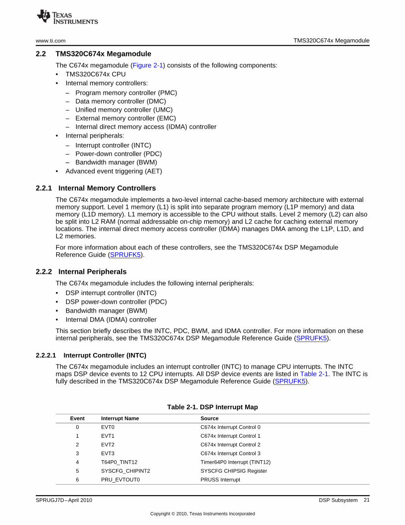
The C674x megamodule includes an interrupt controller (INTC) to manage CPU interrupts. The INTCmaps DSP device events to 12 CPU interrupts. All DSP device events are listed in Table 2-1. The INTC isfully described in the TMS320C674x DSP Megamodule Reference Guide (SPRUFK5).
Table 2-1. DSP Interrupt Map
Event Interrupt Name Source
0 EVT0 C674x Interrupt Control 0
1 EVT1 C674x Interrupt Control 1
2 EVT2 C674x Interrupt Control 2
3 EVT3 C674x Interrupt Control 3
4 T64P0_TINT12 Timer64P0 Interrupt (TINT12)
5 SYSCFG_CHIPINT2 SYSCFG CHIPSIG Register
6 PRU_EVTOUT0 PRUSS Interrupt
21SPRUGJ7D–April 2010 DSP Subsystem
Copyright © 2010, Texas Instruments Incorporated

TMS320C674x Megamodule www.ti.com
Table 2-1. DSP Interrupt Map (continued)
Event Interrupt Name Source
7 EHRPWM0 HiResTimer/PWM0 Interrupt
8 EDMA3_0_CC0_INT1 EDMA3_0 Channel Controller 0 Shadow Region 1 TransferCompletion Interrupt
9 EMU-DTDMA C674x-ECM
10 EHRPWM0TZ HiResTimer/PWM0 Trip Zone Interrupt
11 EMU-RTDXRX C674x-RTDX
12 EMU-RTDXTX C674x-RTDX
13 IDMAINT0 C674x-EMC
14 IDMAINT1 C674x-EMC
15 MMCSD0_INT0 MMCSD0 MMC/SD Interrupt
16 MMCSD0_INT1 MMCSD0 SDIO Interrupt
17 PRU_EVTOUT1 PRUSS Interrupt
18 EHRPWM1 HiResTimer/PWM1 Interrupt
19 USB0_INT USB0 (USB2.0) Interrupt
20 USB1_HCINT USB1 (USB1.1) OHCI Host Controller Interrupt
21 USB1_R/WAKEUP USB1 (USB1.1) Remote Wakeup Interrupt
22 PRU_EVTOUT2 PRUSS Interrupt
23 EHRPWM1TZ HiResTimer/PWM1 Trip Zone Interrupt
24 SATA_INT SATA Controller Interrupt
25 T64P2_TINTALL Timer64P2 Combined Interrupt (TINT12 and TINT34)
26 EMAC_C0RXTHRESH EMAC - Core 0 Receive Threshold Interrupt
27 EMAC_C0RX EMAC - Core 0 Receive Interrupt
28 EMAC_C0TX EMAC - Core 0 Transmit Interrupt
29 EMAC_C0MISC EMAC - Core 0 Miscellaneous Interrupt
30 EMAC_C1RXTHRESH EMAC - Core 1 Receive Threshold Interrupt
31 EMAC_C1RX EMAC - Core 1 Receive Interrupt
32 EMAC_C1TX EMAC - Core 1 Transmit Interrupt
33 EMAC_C1MISC EMAC - Core 1 Miscellaneous Interrupt
34 UHPI_DSPINT HPI DSP Interrupt
35 PRU_EVTOUT3 PRUSS Interrupt
36 IIC0_INT I2C0 Interrupt
37 SPI0_INT SPI0 Interrupt
38 UART0_INT UART0 Interrupt
39 PRU_EVTOUT5 PRUSS Interrupt
40 T64P1_TINT12 Timer64P1 Interrupt (TINT12)
41 GPIO_B1INT GPIO Bank 1 Interrupt
42 IIC1_INT I2C1 Interrupt
43 SPI1_INT SPI1 Interrupt
44 PRU_EVTOUT6 PRUSS Interrupt
45 ECAP0 ECAP0 Interrupt
46 UART_INT1 UART1 Interrupt
47 ECAP1 ECAP1 Interrupt
48 T64P1_TINT34 Timer64P1 Interrupt (TINT34)
49 GPIO_B2INT GPIO Bank 2 Interrupt
50 PRU_EVTOUT7 PRUSS Interrupt
51 ECAP2 ECAP2 Interrupt
52 GPIO_B3INT GPIO Bank 3 Interrupt
53 MMCSD1_INT1 MMCSD1 SDIO Interrupt
22 DSP Subsystem SPRUGJ7D–April 2010
Copyright © 2010, Texas Instruments Incorporated

www.ti.com TMS320C674x Megamodule
Table 2-1. DSP Interrupt Map (continued)
Event Interrupt Name Source
54 GPIO_B4INT GPIO Bank 4 Interrupt
55 EMIFA_INT EMIFA Interrupt
56 EDMA3_0_CC0_ERRINT EDMA3_0 Channel Controller 0 Error Interrrupt
57 EDMA3_0_TC0_ERRINT EDMA3_0 Transfer Controller 0 Error Interrrupt
58 EDMA3_0_TC1_ERRINT EDMA3_0 Transfer Controller 1 Error Interrrupt
59 GPIO_B5INT GPIO Bank 5 Interrupt
60 DDR2_MEMERR DDR2 Memory Error Interrupt
61 MCASP0_INT McASP0 Combined RX/TX Interrupt
62 GPIO_B6INT GPIO Bank 6 Interrupt
63 RTC_IRQS RTC Combined Interrupt
64 T64P0_TINT34 Timer64P0 Interrupt (TINT34)
65 GPIO_B0INT GPIO Bank 0 Interrupt
66 PRU_EVTOUT4 PRUSS Interrupt
67 SYSCFG_CHIPINT3 SYSCFG CHIPSIG Register
68 MMCSD1_INT0 MMCSD1 MMC/SD Interrupt
69 UART2_INT UART2 Interrupt
70 PSC0_ALLINT PSC0
71 PSC1_ALLINT PSC1
72 GPIO_B7INT GPIO Bank 7 Interrupt
73 LCDC_INT LCD Controller Interrupt
74 PROTERR SYSCFG Protection Shared Interrupt
75 GPIO_B8INT GPIO Bank 8 Interrupt
76-77 — Reserved
78 T64P2_CMPINT0 Timer64P2 - Compare Interrupt 0
79 T64P2_CMPINT1 Timer64P2 - Compare Interrupt 1
80 T64P2_CMPINT2 Timer64P2 - Compare Interrupt 2
81 T64P2_CMPINT3 Timer64P2 - Compare Interrupt 3
82 T64P2_CMPINT4 Timer64P2 - Compare Interrupt 4
83 T64P2_CMPINT5 Timer64P2 - Compare Interrupt 5
84 T64P2_CMPINT6 Timer64P2 - Compare Interrupt 6
85 T64P2_CMPINT7 Timer64P2 - Compare Interrupt 7
86 T64P3_TINTALL Timer64P3 Combined Interrupt (TINT12 and TINT34)
87 MCBSP0_RINT McBSP0 Receive Interrupt
88 MCBSP0_XINT McBSP0 Transmit Interrupt
89 MCBSP1_RINT McBSP1 Receive Interrupt
90 MCBSP1_XINT McBSP1 Transmit Interrupt
91 EDMA3_1_CC0_INT1 EDMA3_1 Channel Controller 0 Shadow Region 1 TransferCompletion Interrupt
92 EDMA3_1_CC0_ERRINT EDMA3_1 Channel Controller 0 Error Interrrupt
93 EDMA3_1_TC0_ERRINT EDMA3_1 Transfer Controller 0 Error Interrrupt
94 UPP_INT uPP Combined Interrupt
95 VPIF_INT VPIF Combined Interrupt
96 INTERR C674x-Interrupt Control
97 EMC_IDMAERR C674x-EMC
98-112 — Reserved
113 PMC_ED C674x-PMC
114-115 — Reserved
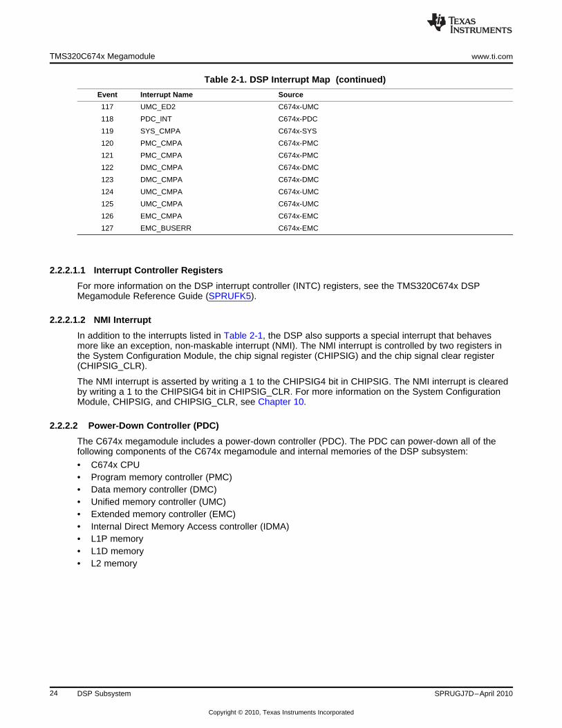
116 UMC_ED1 C674x-UMC
23SPRUGJ7D–April 2010 DSP Subsystem
Copyright © 2010, Texas Instruments Incorporated
TMS320C674x Megamodule www.ti.com
Table 2-1. DSP Interrupt Map (continued)
Event Interrupt Name Source
117 UMC_ED2 C674x-UMC
118 PDC_INT C674x-PDC
119 SYS_CMPA C674x-SYS
120 PMC_CMPA C674x-PMC
121 PMC_CMPA C674x-PMC
122 DMC_CMPA C674x-DMC
123 DMC_CMPA C674x-DMC
124 UMC_CMPA C674x-UMC
125 UMC_CMPA C674x-UMC
126 EMC_CMPA C674x-EMC
127 EMC_BUSERR C674x-EMC
2.2.2.1.1 Interrupt Controller Registers
For more information on the DSP interrupt controller (INTC) registers, see the TMS320C674x DSPMegamodule Reference Guide (SPRUFK5).
2.2.2.1.2 NMI Interrupt
In addition to the interrupts listed in Table 2-1, the DSP also supports a special interrupt that behavesmore like an exception, non-maskable interrupt (NMI). The NMI interrupt is controlled by two registers inthe System Configuration Module, the chip signal register (CHIPSIG) and the chip signal clear register(CHIPSIG_CLR).
The NMI interrupt is asserted by writing a 1 to the CHIPSIG4 bit in CHIPSIG. The NMI interrupt is clearedby writing a 1 to the CHIPSIG4 bit in CHIPSIG_CLR. For more information on the System ConfigurationModule, CHIPSIG, and CHIPSIG_CLR, see Chapter 10.
2.2.2.2 Power-Down Controller (PDC)
The C674x megamodule includes a power-down controller (PDC). The PDC can power-down all of thefollowing components of the C674x megamodule and internal memories of the DSP subsystem:
• C674x CPU• Program memory controller (PMC)• Data memory controller (DMC)• Unified memory controller (UMC)• Extended memory controller (EMC)• Internal Direct Memory Access controller (IDMA)• L1P memory• L1D memory• L2 memory
24 DSP Subsystem SPRUGJ7D–April 2010
Copyright © 2010, Texas Instruments Incorporated

www.ti.com TMS320C674x Megamodule
This device supports the static power-down feature from the C674x megamodule. The TMS320C674xDSP Megamodule Reference Guide (SPRUFK5) describes the power-down control in more detail.
• Static power-down: The PDC initiates power-down (clock gating) of the entire C674x megamodule andall internal memories immediately upon command from software.
Static power-down (clock gating) affects all components of the C674x megamodule and all internalmemories. Software can initiate static power-down by way of a register bit in the power-down controllercommand register (PDCCMD) of the PDC. For more information on the PDC, see the TMS320C674x DSPMegamodule Reference Guide (SPRUFK5).
2.2.2.3 Bandwidth Manager (BWM)
The bandwidth manager (BWM) provides a programmable interface for optimizing bandwidth among therequesters for resources, which include the following:• EDMA-initiated DMA transfers (and resulting coherency operations)• IDMA-initiated transfers (and resulting coherency operations)• Programmable cache coherency operations
– Block based coherency operations– Global coherency operations
• CPU direct-initiated transfers
– Data access (load/store)– Program access
The resources include the following:• L1P memory• L1D memory• L2 memory• Resources outside of the C674x megamodule: external memory, on-chip peripherals, registers
Since any given requestor could potentially block a resource for extended periods of time, the bandwidthmanager is implemented to assure fairness for all requesters.
The bandwidth manager implements a weighted-priority-driven bandwidth allocation. Each requestor(EDMA, IDMA, CPU, etc.) is assigned a priority level on a per-transfer basis. The programmable prioritylevel has a single meaning throughout the system. There are a total of nine priority levels, where priorityzero is the highest priority and priority eight is the lowest priority. When requests for a single resourcecontend, access is granted to the highest-priority requestor. When the contention occurs for multiplesuccessive cycles, a contention counter assures that the lower-priority requestor gets access to theresource every 1 out of n arbitration cycles, where n is programmable. A priority level of -1 represents atransfer whose priority has been increased due to expiration of the contention counter or a transfer that isfixed as the highest-priority transfer to a given resource.
2.2.2.4 Internal DMA (IDMA) Controller
The IDMA controller performs fast block transfers between any two memory locations local to the C674xmegamodule. Local memory locations are defined as those in Level 1 program (L1P), Level 1 data (L1D),and Level 2 (L2) memories, or in the external peripheral configuration (CFG) memory. The IDMA cannottransfer data to or from the internal MMR space. The IDMA is fully described in the TMS320C674x DSPMegamodule Reference Guide (SPRUFK5).
25SPRUGJ7D–April 2010 DSP Subsystem
Copyright © 2010, Texas Instruments Incorporated

Memory Map www.ti.com
2.3 Memory Map
Refer to your device-specific data manual for memory-map information.
2.3.1 DSP Internal Memory
See Section 4.2 for a description of the DSP internal memory.
2.3.2 External Memory
See Chapter 3 and Chapter 4 for a description of the additional system memory and peripherals that theDSP has access to.
2.4 Advanced Event Triggering (AET)
The C674x megamodule supports advanced event triggering (AET). This capability can be used to debugcomplex problems as well as understand performance characteristics of user applications. AET providesthe following capabilities:
• Hardware Program Breakpoints: specify addresses or address ranges that can generate events suchas halting the processor or triggering the trace capture.
• Data Watchpoints: specify data variable addresses, address ranges, or data values that can generateevents such as halting the processor or triggering the trace capture.
• Counters: count the occurrence of an event or cycles for performance monitoring.• State Sequencing: allows combinations of hardware program breakpoints and data watchpoints to
precisely generate events for complex sequences.
26 DSP Subsystem SPRUGJ7D–April 2010
Copyright © 2010, Texas Instruments Incorporated

Chapter 3SPRUGJ7D–April 2010
System Interconnect
Topic ........................................................................................................................... Page
3.1 Introduction ...................................................................................................... 283.2 System Interconnect Block Diagram .................................................................... 29
27SPRUGJ7D–April 2010 System Interconnect
Copyright © 2010, Texas Instruments Incorporated
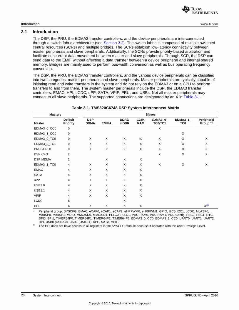
Introduction www.ti.com
3.1 Introduction
The DSP, the PRU, the EDMA3 transfer controllers, and the device peripherals are interconnectedthrough a switch fabric architecture (see Section 3.2). The switch fabric is composed of multiple switchedcentral resources (SCRs) and multiple bridges. The SCRs establish low-latency connectivity betweenmaster peripherals and slave peripherals. Additionally, the SCRs provide priority-based arbitration andfacilitate concurrent data movement between master and slave peripherals. Through SCR, the DSP cansend data to the EMIF without affecting a data transfer between a device peripheral and internal sharedmemory. Bridges are mainly used to perform bus-width conversion as well as bus operating frequencyconversion.
The DSP, the PRU, the EDMA3 transfer controllers, and the various device peripherals can be classifiedinto two categories: master peripherals and slave peripherals. Master peripherals are typically capable ofinitiating read and write transfers in the system and do not rely on the EDMA3 or on a CPU to performtransfers to and from them. The system master peripherals include the DSP, the EDMA3 transfercontrollers, EMAC, HPI, LCDC, uPP, SATA, VPIF, PRU, and USBs. Not all master peripherals mayconnect to all slave peripherals. The supported connections are designated by an X in Table 3-1.
Table 3-1. TMS320C6748 DSP System Interconnect Matrix
Masters Slaves
Default DSP DDR2/ 128K EDMA3_0_ EDMA3_1_ PeripheralMaster Priority SDMA EMIFA mDDR RAM TC0/TC1 TC0 Group (1)
EDMA3_0_CC0 0 X
EDMA3_1_CC0 0 X
EDMA3_0_TC0 0 X X X X X X X
EDMA3_0_TC1 0 X X X X X X X
PRU0/PRU1 0 X X X X X X X
DSP CFG 2 X X X
DSP MDMA 2 X X X
EDMA3_1_TC0 4 X X X X X X X
EMAC 4 X X X X
SATA 4 X X X X
uPP 4 X X X X
USB2.0 4 X X X X
USB1.1 4 X X X X
VPIF 4 X X X X
LCDC 5 X
HPI 6 X X X X X (2)
(1) Peripheral group: SYSCFG, EMAC, eCAP0, eCAP1, eCAP2, eHRPWM0, eHRPWM1, GPIO, I2C0, I2C1, LCDC, McASP0,McBSP0, McBSP1, MDIO, MMC/SD0, MMC/SD1, PLLC0, PLLC1, PRU RAM0, PRU RAM1, PRU Config, PSC0, PSC1, RTC,SPI0, SPI1, TIMER64P0, TIMER64P1, TIMER64P2, TIMER64P3, EDMA3_0_CC0, EDMA3_1_CC0, UART0, UART1, UART2,HPI, USB0 (USB2.0), USB1 (USB1.1), uPP, SATA, VPIF.
(2) The HPI does not have access to all registers in the SYSCFG module because it operates with the User Privilege Level.
28 System Interconnect SPRUGJ7D–April 2010
Copyright © 2010, Texas Instruments Incorporated

Legend:
32-bit BUS
64-bit BUS
IP Module
Synchronous Bridge
Asynchronous Bridge
SCR
Paths with dashed lines cross the subchip boundary
HPI
USB0 CDMA
USB0 VBUSP
SCR F0
EMAC
USB1SCR F1 BR F1
EDMA3_0_TC0rd
wr
EDMA3_0_TC1rd
wr
EDMA3_1_TC0rd
wr
DSP MDMA
uPP DMA
VPIF DMA0
VPIF DMA1SCR F2
SATA
BR F0
BR F2
SCR1
BR3 BR4
SCR2
DSP CFG
EDMA3_0_CC0 EDMA3_0_CC0
DSP SDMA (L1D/L2)
BR F6 SCR F4 MPU1
BR F7SCR F3
LCDCDDR2/mDDR
BR5
SCR5
PSC0
PLLC0
SYSCFG0
Clock Domain: SYSCLK4 [CPU/4 Synchronous]
BR6
SCR6
Timer64P0
Timer64P1
I2C0
RTC
Async 2 Clock Domain
BR7
Async 1 Clock Domain
EMIFA
SCR4
MMC/SD0
SPI0
UART0
EDMA3_0_TC0
EDMA3_0_TC1
SCR F5
EDMA3_0_CC1
EDMA3_1_ CC0
USB0 Cfg
HPI
LCDC
EDMA3_0_CC1
uPP
VPIF
SATA
MMC/SD1
BR F3
SCR F6
SYSCFG1
EMAC
EMAC MDIO
USB1 Cfg
GPIO
PSC1
I2C1
PLLC1
Clock Domain: SYSCLK4 [CPU/4 Synchronous]
BR F4
BR F5
SCR F7
McBSP0
McBSP1
UART1
UART2
McASP0
SCR F8
eHRPWM0
eHRPWM1
Timer64P2
Timer64P3
eCAP0
eCAP1
eCAP2
SPI1
Async 3 [PLL1] Clock Domain
Clock Domain: SYSCLK4 [CPU/4 Synchronous]
PRU0
PRU1
PRU CFG
`128 KBShared RAM
MPU2
www.ti.com System Interconnect Block Diagram
3.2 System Interconnect Block Diagram
Figure 3-1 shows a system interconnect block diagram.
Figure 3-1. System Interconnect Block Diagram
29SPRUGJ7D–April 2010 System Interconnect
Copyright © 2010, Texas Instruments Incorporated

30 System Interconnect SPRUGJ7D–April 2010
Copyright © 2010, Texas Instruments Incorporated

Chapter 4SPRUGJ7D–April 2010
System Memory
Topic ........................................................................................................................... Page
4.1 Introduction ...................................................................................................... 324.2 DSP Memories .................................................................................................. 324.3 Shared RAM Memory ......................................................................................... 324.4 External Memories ............................................................................................. 324.5 Internal Peripherals ........................................................................................... 334.6 Peripherals ....................................................................................................... 33
31SPRUGJ7D–April 2010 System Memory
Copyright © 2010, Texas Instruments Incorporated

Introduction www.ti.com
4.1 Introduction
This device has multiple on-chip/off-chip memories and several external device interfaces associated withthe DSP and various subsystems. To help simplify software development, a unified memory-map is usedwherever possible to maintain a consistent view of device resources across all masters (CPU and masterperipherals).
For details on the memory addresses, actual memory supported and accessibility by various bus masters,see the detailed memory-map information in the device-specific data manual.
4.2 DSP Memories
The DSP internal memories are accessible by the DSP and other master peripherals (as dictated by theconnectivity matrix) via the system interconnect through the DSP SDMA port. The accesses by the DSP toits internal memory are internal to the DSP subsystem and do not go out on the system interconnect.
The DSP internal memory consists of L1P, L1D, and L2. The DSP internal memory configuration is:
• L1P memory includes 32 KB of RAM. The DSP program memory controller (PMC) allows you toconfigure part or all of the L1P RAM as normal program RAM or as cache. You can configure cachesizes of 0 KB, 4 KB, 8 KB, 16 KB, or 32 KB of the 32 KB of RAM. The default configuration is 32 KBcache.
• L1D memory includes 32 KB of RAM. The DSP data memory controller (DMC) allows you to configurepart of the L1D RAM as normal data RAM or as cache. You can configure cache sizes of 0 KB, 4 KB,8 KB, 16 KB, or 32 KB of the 32 KB of RAM. The default configuration is 32 KB cache.
• L2 memory includes 256 KB of RAM. The DSP unified memory controller (UMC) allows you toconfigure part or all of the L2 RAM as normal RAM or as cache. You can configure cache sizes of 0KB, 4 KB, 8 KB, 16 KB, 32 KB, 64 KB, 128 KB, or 256 KB of the 256 KB of RAM. The defaultconfiguration is 256 KB normal RAM.
• L2 memory also includes 1024 KB of ROM.
4.3 Shared RAM Memory
This device also offers an on-chip 128-KB shared RAM, apart from the DSP level 1 and level 2 internalmemories. This shared RAM is accessible by the DSP, and also is accessible by several masterperipherals.
4.4 External Memories
This device has two external memory interfaces that provide multiple external memory options accessibleby the CPU and master peripherals:
• EMIFA:
– 8/16-bit wide (package dependent) asynchronous EMIF module that supports asynchronousdevices such as ASRAM, NAND Flash, and NOR Flash (up to 4 devices)
– 8/16-bit wide (package dependent) NAND Flash with 4-bit ECC (up to 4 devices)– 16-bit SDRAM with 128-MB address space (package dependent)
• DDR2/mDDR memory controller:
– 16-bit DDR2 with up to 512-MB memory address space– 16-bit mDDR with up to 256-MB memory address space
32 System Memory SPRUGJ7D–April 2010
Copyright © 2010, Texas Instruments Incorporated

www.ti.com Internal Peripherals
4.5 Internal Peripherals
The following peripherals are internal to the DSP subsystem and are only accessible to the DSP:• DSP interrupt controller (INTC)• DSP power down controller (PDC)• Bandwidth manager (BWM)• Internal DMA (IDMA)
For more information on the internal peripherals, see the TMS320C674x DSP Megamodule ReferenceGuide (SPRUFK5).
4.6 Peripherals
The DSP has access to all peripherals on the device. See the device-specific data manual for thecomplete list of peripherals supported on your device.
33SPRUGJ7D–April 2010 System Memory
Copyright © 2010, Texas Instruments Incorporated

34 System Memory SPRUGJ7D–April 2010
Copyright © 2010, Texas Instruments Incorporated

Chapter 5SPRUGJ7D–April 2010
Memory Protection Unit (MPU)
Topic ........................................................................................................................... Page
5.1 Introduction ...................................................................................................... 365.2 Architecture ...................................................................................................... 375.3 MPU Registers .................................................................................................. 42
35SPRUGJ7D–April 2010 Memory Protection Unit (MPU)
Copyright © 2010, Texas Instruments Incorporated

ProtectionChecks
MMRs
MPU_ADDR_ERR_INT
MPU_PROT_ERR_INT
OutputDataBus
MPU Register Bus
InputDataBus
MPU
Introduction www.ti.com
5.1 Introduction
This device supports two memory protection units (MPU1 and MPU2). MPU1 supports the 128KB sharedRAM and MPU2 supports the DDR2/mDDR SDRAM.
5.1.1 Purpose of the MPU
The memory protection unit (MPU) is provided to manage access to memory. The MPU allows you todefine multiple ranges and limit access to system masters based on their privilege ID. The MPU canrecord a detected fault, or invalid access, and notify the system through an interrupt.
5.1.2 Features
The MPU supports the following features:
• Supports multiple programmable address ranges• Supports 0 or 1 fixed range• Supports read, write, and execute access privileges• Supports privilege ID associations with ranges• Generates an interrupt when there is a protection violation, and saves violating transfer parameters• Supports L1/L2 cache accesses• Supports protection of its own registers
5.1.3 Block Diagram
Figure 5-1shows a block diagram of the MPU. An access to a protected memory must pass through theMPU. During an access, the MPU checks the memory address on the input data bus against fixed andprogrammable ranges. If allowed, the transfer is passed unmodified to the output data bus. If the transferfails the protection check then the MPU does not pass the transfer to the output bus but rather servicesthe transfer internally back to the input bus (to prevent a hang) returning the fault status to the requestoras well as generating an interrupt about the fault. The MPU generates two interrupts: an address errorinterrupt (MPU_ADDR_ERR_INT) and a protection interrupt (MPU_PROT_ERR_INT).
Figure 5-1. MPU Block Diagram
36 Memory Protection Unit (MPU) SPRUGJ7D–April 2010
Copyright © 2010, Texas Instruments Incorporated

www.ti.com Architecture
5.1.4 MPU Default Configuration
Two MPUs are supported on the device, one for the 128KB shared RAM and one for the DDR2/mDDRSDRAM. Table 5-1shows the memory regions protected by each MPU. Table 5-2shows the configurationof each MPU.
Table 5-1. MPU Memory Regions
Memory Region
Unit Memory Protection Start Address End Address
MPU1 128KB Shared RAM 8000 0000h 8001 FFFFh
MPU2 DDR2/mDDR SDRAM C000 0000h DFFF FFFFh
Table 5-2. MPU Default Configuration
Setting MPU1 MPU2
Default permission Assume allowed Assume allowed
Number of allowed IDs supported 12 12
Number of fixed ranges supported 1 0
Number of programmable ranges supported 6 12
Compare width 1 KB granularity 64 KB granularity
5.2 Architecture
5.2.1 Privilege Levels
The privilege level of a memory access determines what level of permissions the originator of the memoryaccess might have. Two privilege levels are supported: supervisor and user.
Supervisor level is generally granted access to peripheral registers and the memory protectionconfiguration. User level is generally confined to the memory spaces that the OS specifically designatesfor its use.
DSP CPU instruction and data accesses have a privilege level associated with them. The privilege level isinherited from the code running on the CPU. See the TMS320C674x DSP CPU and Instruction SetReference Guide (SPRUFE8) for more details on privilege levels of the DSP CPU.
Although master peripherals like the HPI do not execute code, they still have a privilege level associatedwith them. Unlike the DSP CPU, the privilege level of this peripheral is fixed.
Table 5-3 shows the privilege ID of the CPU and every mastering peripheral. Table 5-3 also shows theprivilege level (supervisor vs. user) and access type (instruction read vs. data/DMA read or write) of eachmaster on the device. In some cases, a particular setting depends on software being executed at the timeof the access or the configuration of the master peripheral.
Table 5-3. Device Master Settings
Master Privilege ID Privilege Level Access Type
EDMA3_0_CC0 Inherited Inherited DMA
EDMA3_0_TC0 and EDMA3_0_TC1 Inherited Inherited DMA
EDMA3_1_CC0 Inherited Inherited DMA
EDMA3_1_TC0 Inherited Inherited DMA
DSP 1 Software dependant Software dependant
PRU0/PRU1 2 Supervisor DMA
37SPRUGJ7D–April 2010 Memory Protection Unit (MPU)
Copyright © 2010, Texas Instruments Incorporated

Architecture www.ti.com
Table 5-3. Device Master Settings (continued)
Master Privilege ID Privilege Level Access Type
HPI 3 User DMA
EMAC 4 Supervisor Data/DMA
USB1.1 5 Supervisor DMA
USB2.0 6 Supervisor DMA
LCD Controller 7 Supervisor DMA
uPP 8 Supervisor DMA
SATA 9 Supervisor DMA
VPIF DMA0 10 Supervisor DMA
VPIF DMA1 11 Supervisor DMA
5.2.2 Memory Protection Ranges
NOTE: In some cases the amount of physical memory in actual use may be less than the maximumamount of memory supported by the device. For example, the device may support a total of512 Mbytes of SDRAM memory, but your design may only populate 128 Mbytes. In suchcases, the unpopulated memory range must be protected in order to preventunintended/disallowed aliased access to protected memory. One of the programmableaddress ranges could be used to detect accesses to this unpopulated memory.
The MPU divides its assigned memory into address ranges. Each MPU can support one fixed addressrange and multiple programmable address ranges. The fixed address range is configured to an exactaddress. The programmable address range allows software to program the start and end addresses.
Each address range has the following set of registers:
• Range start and end address registers (MPSAR and MPEAR): Specifies the starting and endingaddress of the address range.
• Memory protection page attribute register (MPPA): Use to program the permission settings of theaddress range.
It is allowed to configure ranges such that they overlap each other. In this case, all the overlapped rangesmust allow the access, otherwise the access is not allowed. The final permissions given to the access arethe lowest of each type of permission from any hit range.
Addresses not covered by a range are either allowed or disallowed based on the configuration of theMPU. The MPU can be configured for assumed allowed or assumed disallowed mode as dictated by theASSUME_ALLOWED bit in the configuration register (CONFIG).
5.2.3 Permission Structures
The MPU defines a per-range permission structure with three permission fields in a 32-bit permissionentry. Table 5-4 shows the structure of a permission entry.
Table 5-4. Permission Fields
31 22 21 20 19 18 17 16
Reserved Allowed IDs
AID11 AID10 AID9 AID8 AID7 AID6
15 14 13 12 11 10 9 8 6 5 4 3 2 1 0
Allowed IDs Reserved Access Types
AID5 AID4 AID3 AID2 AID1 AID0 AIX SR SW SX UR UW UX
38 Memory Protection Unit (MPU) SPRUGJ7D–April 2010
Copyright © 2010, Texas Instruments Incorporated

www.ti.com Architecture
5.2.3.1 Requestor-ID Based Access Controls
Each master on the device has an N-bit code associated with it that identifies it for privilege purposes.This privilege ID accompanies all memory accesses made on behalf of that master. That is, when amaster triggers a memory access command, the privilege ID will be carried alongside the command.
Each memory protection range has an allowed ID (AID) field associated with it that indicates whichrequestors may access the given address range. The MPU maps the privilege IDs of all the possiblerequestors to bits in the allowed IDs field in the memory protection page attribute registers (MPPA).
• AID0 through AID11 are used to specify the allowed privilege IDs.• An additional allowed ID bit, AIDX, captures access made by all privilege IDs not covered by AID0
through AID11.
When set to 1, the AID bit grants access to the corresponding ID. When cleared to 0, the AID bit deniesaccess to the corresponding requestor.
5.2.3.2 Request-Type Based Permissions
The memory protection model defines three fundamental functional access types: read, write, andexecute. Read and write refer to data accesses -- accesses originating via the load/store units on the CPUor via a master peripheral. Execute refers to accesses associated with an instruction fetch.
The memory protection model allows controlling read, write, and execute permissions independently forboth user and supervisor mode. This results in six permission bits, listed in Table 5-5. For each bit, a 1permits the access type and a 0 denies access. For example, UX = 1 means that User Mode may executefrom the given page. The memory protection unit allows you to specify all six of these bits separately; 64different encodings are permitted altogether, although programs might not use all of them.
Table 5-5. Request Type Access Controls
Bit Field Description
5 SR Supervisor may read
4 SW Supervisor may write
3 SX Supervisor may execute
2 UR User may read
1 UW User may write
0 UX User may execute
39SPRUGJ7D–April 2010 Memory Protection Unit (MPU)
Copyright © 2010, Texas Instruments Incorporated

Architecture www.ti.com
5.2.4 Protection Check
During a memory access, the MPU checks if the address range of the input transfer overlaps one of theaddress ranges. When the input transfer address is within a range the transfer parameters are checkedagainst the address range permissions.
The MPU first checks the transfers privilege ID against the AID settings. If the AID bit is 0, then the rangewill not be checked; if the AID bit is 1, then the transfer parameters are checked against the memoryprotection page attribute register (MPPA) values to detect an allowed access.
For non-debug accesses, the read, write, and execute permissions are also checked. There is a set ofpermissions for supervisor mode and a set for user mode. For supervisor mode accesses, the SR, SW,and SX bits are checked. For user mode accesses, the UR, UW, and UX bits are checked.
If the transfer address range does not match any address range then the transfer is either allowed ordisallowed based on the configuration of the MPU. The MPU can be configured for assumed allowed orassumed disallowed mode as dictated by the ASSUME_ALLOWED bit in the configuration register(CONFIG).
In the case that a transfer spans multiple address ranges, all the overlapped ranges must allow theaccess, otherwise the access is not allowed. The final permissions given to the access are the lowest ofeach type of permission from any hit range. Therefore, if a transfer matches 2 ranges, one that is RW andone that is RX, then the final permission is just R.
The MPU has a special mechanism for handling DSP L1/L2 cache controller read accesses, see for moredetails.
5.2.5 DSP L1/L2 Cache Controller Accesses
A memory read access that originates from the DSP L1/L2 cache is treated differently to allow memoryprotection to be enforced by the DSP level. This is because a subsequent memory access that hits in thecache does not pass through the MPU. Instead the memory access is serviced directly by the L1/L2memory controllers.
During a cache memory read, the permission settings stored in the memory protection page attributeregisters (MPPA) are passed to the L1/L2 memory controllers along with the read data. The permissionssettings returned by the MPU are taken from MPPA that covers the address range of the originalrequest—only the SR, SW, SX, UR, UW, and UX bits are passed. If the request address is covered bymultiple address ranges, then the returned value is the logical-AND of all MPPA permissions. If thetransfer address range is not covered by an address range then the transfer is either allowed ordisallowed based on the configuration of the MPU.
5.2.6 MPU Register Protection
Access to the range start and end address registers (MPSAR and MPEAR) and memory protection pageattribute registers (MPPA) is also protected. All non-debug writes must be by a supervisor entity. Aprotection fault can occur from a register write with invalid permissions and this triggers an interrupt justlike a memory access.
Faults are not recorded (nor interrupts generated) for debug accesses.
40 Memory Protection Unit (MPU) SPRUGJ7D–April 2010
Copyright © 2010, Texas Instruments Incorporated

www.ti.com Architecture
5.2.7 Invalid Accesses and Exceptions
When a transfer fails the protection check, the MPU does not pass the transfer to the output bus. TheMPU instead services the transfer locally to prevent a hang and returns a protection error to the requestor.The behavior of the MPU depends on whether the access was a read or a write:
• For a read: The MPU returns 0s, a permission value is 0 (no access allowed), a protection error status.• For a write: The MPU receives all the write data and returns a protection error status.
The MPU captures system faults due to addressing or protection violations in its registers. The MPU canstore the fault information for only one fault, so the first detected fault is recorded into the fault registersand an interrupt is generated. Software must use the fault clear register (FLTCLR) to clear the fault statusso that another fault can be recorded. The MPU will not record another fault nor generate another interruptuntil the existing fault has been cleared. Also, additional faults will be ignored. Faults are not recorded (nointerrupts generated) for debug accesses.
5.2.8 Reset Considerations
After reset, the memory protection page attribute registers (MPPA) default to 0. This disables all protectionfeatures.
5.2.9 Interrupt Support
5.2.9.1 Interrupt Events and Requests
The MPU generates two interrupts: an address error interrupt (MPU_ADDR_ERR_INT) and a protectioninterrupt (MPU_PROT_ERR_INT). The MPU_ADDR_ERR_INT is generated when there is an addressingviolation due to an access to a non-existent location in the MPU register space. TheMPU_PROT_ERR_INT interrupt is generated when there is a protection violation of either in the definedranges or to the MPU registers.
The transfer parameters that caused the violation are saved in the MPU registers.
5.2.9.2 Interrupt Multiplexing
The interrupts from both MPUs are combined with the boot configuration module into a single interruptcalled MPU_BOOTCFG_ERR. The combined interrupt is routed to the DSP interrupt controller. Table 5-6shows the interrupt sources that are combined to make MPU_BOOTCFG_ERR.
Table 5-6. MPU_BOOTCFG_ERR Interrupt Sources
Interrupt Source
MPU1_ADDR_ERR_INT MPU1 address error interrupt
MPU1_PROT_ERR_INT MPU1 protection interrupt
MPU2_ADDR_ERR_INT MPU2 address error interrupt
MPU2_PROT_ERR_INT MPU2 protection interrupt
BOOTCFG_ADDR_ERR Boot configuration address error
BOOTCFG_PROT_ERR Boot configuration protection error
5.2.10 Emulation Considerations
Memory and MPU registers are not protected against emulation accesses.
41SPRUGJ7D–April 2010 Memory Protection Unit (MPU)
Copyright © 2010, Texas Instruments Incorporated

MPU Registers www.ti.com
5.3 MPU Registers
There are two MPUs on the device. Each MPU contains a set of memory-mapped registers.
Table 5-7 lists the memory-mapped registers for the MPU1. Table 5-8 lists the memory-mapped registersfor the MPU2.
Table 5-7. Memory Protection Unit 1 (MPU1) Registers
Address Acronym Register Description Section
01E1 4000h REVID Revision identification register Section 5.3.1
01E1 4004h CONFIG Configuration register Section 5.3.2
01E1 4010h IRAWSTAT Interrupt raw status/set register Section 5.3.3
01E1 4014h IENSTAT Interrupt enable status/clear register Section 5.3.4
01E1 4018h IENSET Interrupt enable set register Section 5.3.5
01E1 401Ch IENCLR Interrupt enable clear register Section 5.3.6
01E1 4200h PROG1_MPSAR Programmable range 1 start address register Section 5.3.10.1
01E1 4204h PROG1_MPEAR Programmable range 1 end address register Section 5.3.11.1
01E1 4208h PROG1_MPPA Programmable range 1 memory protection page attributes register Section 5.3.12
01E1 4210h PROG2_MPSAR Programmable range 2 start address register Section 5.3.10.1
01E1 4214h PROG2_MPEAR Programmable range 2 end address register Section 5.3.11.1
01E1 4218h PROG2_MPPA Programmable range 2 memory protection page attributes register Section 5.3.12
01E1 4220h PROG3_MPSAR Programmable range 3 start address register Section 5.3.10.1
01E1 4224h PROG3_MPEAR Programmable range 3 end address register Section 5.3.11.1
01E1 4228h PROG3_MPPA Programmable range 3 memory protection page attributes register Section 5.3.12
01E1 4230h PROG4_MPSAR Programmable range 4 start address register Section 5.3.10.1
01E1 4234h PROG4_MPEAR Programmable range 4 end address register Section 5.3.11.1
01E1 4238h PROG4_MPPA Programmable range 4 memory protection page attributes register Section 5.3.12
01E1 4240h PROG5_MPSAR Programmable range 5 start address register Section 5.3.10.1
01E1 4244h PROG5_MPEAR Programmable range 5 end address register Section 5.3.11.1
01E1 4248h PROG5_MPPA Programmable range 5 memory protection page attributes register Section 5.3.12
01E1 4250h PROG6_MPSAR Programmable range 6 start address register Section 5.3.10.1
01E1 4254h PROG6_MPEAR Programmable range 6 end address register Section 5.3.11.1
01E1 4258h PROG6_MPPA Programmable range 6 memory protection page attributes register Section 5.3.12
01E1 4300h FLTADDRR Fault address register Section 5.3.13
01E1 4304h FLTSTAT Fault status register Section 5.3.14
01E1 4308h FLTCLR Fault clear register Section 5.3.15
Table 5-8. Memory Protection Unit 2 (MPU2) Registers
Address Acronym Register Description Section
01E1 5000h REVID Revision identification register Section 5.3.1
01E1 5004h CONFIG Configuration register Section 5.3.2
01E1 5010h IRAWSTAT Interrupt raw status/set register Section 5.3.3
01E1 5014h IENSTAT Interrupt enable status/clear register Section 5.3.4
01E1 5018h IENSET Interrupt enable set register Section 5.3.5
01E1 501Ch IENCLR Interrupt enable clear register Section 5.3.6
01E1 5100h FXD_MPSAR Fixed range start address register Section 5.3.7
01E1 5104h FXD_MPEAR Fixed range end address register Section 5.3.8
01E1 5108h FXD_MPPA Fixed range memory protection page attributes register Section 5.3.9
01E1 5200h PROG1_MPSAR Programmable range 1 start address register Section 5.3.10.2
42 Memory Protection Unit (MPU) SPRUGJ7D–April 2010
Copyright © 2010, Texas Instruments Incorporated
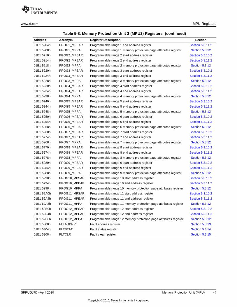
www.ti.com MPU Registers
Table 5-8. Memory Protection Unit 2 (MPU2) Registers (continued)
Address Acronym Register Description Section
01E1 5204h PROG1_MPEAR Programmable range 1 end address register Section 5.3.11.2
01E1 5208h PROG1_MPPA Programmable range 1 memory protection page attributes register Section 5.3.12
01E1 5210h PROG2_MPSAR Programmable range 2 start address register Section 5.3.10.2
01E1 5214h PROG2_MPEAR Programmable range 2 end address register Section 5.3.11.2
01E1 5218h PROG2_MPPA Programmable range 2 memory protection page attributes register Section 5.3.12
01E1 5220h PROG3_MPSAR Programmable range 3 start address register Section 5.3.10.2
01E1 5224h PROG3_MPEAR Programmable range 3 end address register Section 5.3.11.2
01E1 5228h PROG3_MPPA Programmable range 3 memory protection page attributes register Section 5.3.12
01E1 5230h PROG4_MPSAR Programmable range 4 start address register Section 5.3.10.2
01E1 5234h PROG4_MPEAR Programmable range 4 end address register Section 5.3.11.2
01E1 5238h PROG4_MPPA Programmable range 4 memory protection page attributes register Section 5.3.12
01E1 5240h PROG5_MPSAR Programmable range 5 start address register Section 5.3.10.2
01E1 5244h PROG5_MPEAR Programmable range 5 end address register Section 5.3.11.2
01E1 5248h PROG5_MPPA Programmable range 5 memory protection page attributes register Section 5.3.12
01E1 5250h PROG6_MPSAR Programmable range 6 start address register Section 5.3.10.2
01E1 5254h PROG6_MPEAR Programmable range 6 end address register Section 5.3.11.2
01E1 5258h PROG6_MPPA Programmable range 6 memory protection page attributes register Section 5.3.12
01E1 5260h PROG7_MPSAR Programmable range 7 start address register Section 5.3.10.2
01E1 5274h PROG7_MPEAR Programmable range 7 end address register Section 5.3.11.2
01E1 5268h PROG7_MPPA Programmable range 7 memory protection page attributes register Section 5.3.12
01E1 5270h PROG8_MPSAR Programmable range 8 start address register Section 5.3.10.2
01E1 5274h PROG8_MPEAR Programmable range 8 end address register Section 5.3.11.2
01E1 5278h PROG8_MPPA Programmable range 8 memory protection page attributes register Section 5.3.12
01E1 5280h PROG9_MPSAR Programmable range 9 start address register Section 5.3.10.2
01E1 5284h PROG9_MPEAR Programmable range 9 end address register Section 5.3.11.2
01E1 5288h PROG9_MPPA Programmable range 9 memory protection page attributes register Section 5.3.12
01E1 5290h PROG10_MPSAR Programmable range 10 start address register Section 5.3.10.2
01E1 5294h PROG10_MPEAR Programmable range 10 end address register Section 5.3.11.2
01E1 5298h PROG10_MPPA Programmable range 10 memory protection page attributes register Section 5.3.12
01E1 52A0h PROG11_MPSAR Programmable range 11 start address register Section 5.3.10.2
01E1 52A4h PROG11_MPEAR Programmable range 11 end address register Section 5.3.11.2
01E1 52A8h PROG11_MPPA Programmable range 11 memory protection page attributes register Section 5.3.12
01E1 52B0h PROG12_MPSAR Programmable range 12 start address register Section 5.3.10.2
01E1 52B4h PROG12_MPEAR Programmable range 12 end address register Section 5.3.11.2
01E1 52B8h PROG12_MPPA Programmable range 12 memory protection page attributes register Section 5.3.12
01E1 5300h FLTADDRR Fault address register Section 5.3.13
01E1 5304h FLTSTAT Fault status register Section 5.3.14
01E1 5308h FLTCLR Fault clear register Section 5.3.15
43SPRUGJ7D–April 2010 Memory Protection Unit (MPU)
Copyright © 2010, Texas Instruments Incorporated
MPU Registers www.ti.com
5.3.1 Revision Identification Register (REVID)
The revision ID register (REVID) contains the MPU revision. The REVID is shown in Figure 5-2 anddescribed in Table 5-9.
Figure 5-2. Revision ID Register (REVID)31 0
REV
R-4E81 0101h
LEGEND: R = Read only; -n = value after reset
Table 5-9. Revision ID Register (REVID) Field Descriptions
Bit Field Value Description
31-0 REV 4E81 0101h Revision ID of the MPU.
5.3.2 Configuration Register (CONFIG)
The configuration register (CONFIG) contains the configuration value of the MPU. The CONFIG is shownin Figure 5-3 and described in Table 5-10.
NOTE: Although the NUM_AIDS bit defaults to 12 (Ch), not all AIDs may be supported on yourdevice. Unsupported AIDs should be cleared to 0 in the memory page protection attributesregisters (MPPA). See for a list of AIDs supported on your device.
Figure 5-3. Configuration Register (CONFIG)31 24 23 20 19 16
ADDR_WIDTH NUM_FIXED NUM_PROG
R-0 (1) or 6h (2) R-0 (1) or 1 (2) R-6h (1) or Ch (2)
15 12 11 1 0
NUM_AIDS Reserved ASSUME_ALLOWED
R-Ch R-0 R-1
LEGEND: R = Read only; -n = value after reset
(1) For MPU1.(2) For MPU2.
Table 5-10. Configuration Register (CONFIG) Field Descriptions
Bit Field Value Description
31-24 ADDR_WIDTH 0-FFh Address alignment (2n KByte alignment) for range checking.
23-20 NUM_FIXED 0-Fh Number of fixed address ranges.
19-16 NUM_PROG 0-Fh Number of programmable address ranges.
15-12 NUM_AIDS 0-Fh Number of supported AIDs.
11-1 Reserved 0 Reserved
0 ASSUME_ALLOWED Assume allowed. When an address is not covered by any MPU protection range, this bitdetermines whether the transfer is assumed to be allowed or not allowed.
0 Assume is disallowed.
1 Assume is allowed.
44 Memory Protection Unit (MPU) SPRUGJ7D–April 2010
Copyright © 2010, Texas Instruments Incorporated

www.ti.com MPU Registers
5.3.3 Interrupt Raw Status/Set Register (IRAWSTAT)
Reading the interrupt raw status/set register (IRAWSTAT) returns the status of all interrupts. Software canwrite to IRAWSTAT to manually set an interrupt; however, an interrupt is generated only if the interrupt isenabled in the interrupt enable set register (IENSET). Writes of 0 have no effect. The IRAWSTAT isshown in Figure 5-4 and described in Table 5-11.
Figure 5-4. Interrupt Raw Status/Set Register (IRAWSTAT)31 16
Reserved
R-0
15 2 1 0
ADDRERR PROTERR
R-0 R/W-0 R/W-0
LEGEND: R/W = Read/Write; R = Read only; -n = value after reset
Table 5-11. Interrupt Raw Status/Set Register (IRAWSTAT) Field Descriptions
Bit Field Value Description
31-2 Reserved 0 Reserved
1 ADDRERR Address violation error. Reading this bit reflects the status of the interrupt. Writing 1 sets the status;writing 0 has no effect.
0 Interrupt is not set.
1 Interrupt is set.
0 PROTERR Protection violation error. Reading this bit reflects the status of the interrupt. Writing 1 sets thestatus; writing 0 has no effect.
0 Interrupt is not set.
1 Interrupt is set.
45SPRUGJ7D–April 2010 Memory Protection Unit (MPU)
Copyright © 2010, Texas Instruments Incorporated

MPU Registers www.ti.com
5.3.4 Interrupt Enable Status/Clear Register (IENSTAT)
Reading the interrupt enable status/clear register (IENSTAT) returns the status of only those interruptsthat are enabled in the interrupt enable set register (IENSET). Software can write to IENSTAT to clear aninterrupt; the interrupt is cleared from both IENSTAT and the interrupt raw status/set register(IRAWSTAT). Writes of 0 have no effect. The IENSTAT is shown in Figure 5-5 and described inTable 5-12.
Figure 5-5. Interrupt Enable Status/Clear Register (IENSTAT)31 16
Reserved
R-0
15 2 1 0
ADDRERR PROTERR
R-0 R/W-0 R/W-0
LEGEND: R/W = Read/Write; R = Read only; -n = value after reset
Table 5-12. Interrupt Enable Status/Clear Register (IENSTAT) Field Descriptions
Bit Field Value Description
31-2 Reserved 0 Reserved
1 ADDRERR Address violation error. If the interrupt is enabled, reading this bit reflects the status of the interrupt.If the interrupt is disabled, reading this bit returns 0. Writing 1 sets the status; writing 0 has noeffect.
0 Interrupt is not set.
1 Interrupt is set.
0 PROTERR Protection violation error. If the interrupt is enabled, reading this bit reflects the status of theinterrupt. If the interrupt is disabled, reading this bit returns 0. Writing 1 sets the status; writing 0has no effect.
0 Interrupt is not set.
1 Interrupt is set.
46 Memory Protection Unit (MPU) SPRUGJ7D–April 2010
Copyright © 2010, Texas Instruments Incorporated

www.ti.com MPU Registers
5.3.5 Interrupt Enable Set Register (IENSET)
Reading the interrupt enable set register (IENSET) returns the interrupts that are enabled. Software canwrite to IENSET to enable an interrupt. Writes of 0 have no effect. The IENSET is shown in Figure 5-6 anddescribed in Table 5-13.
Figure 5-6. Interrupt Enable Set Register (IENSET)31 16
Reserved
R-0
15 2 1 0
ADDRERR_EN PROTERR_EN
R-0 R/W-0 R/W-0
LEGEND: R/W = Read/Write; R = Read only; -n = value after reset
Table 5-13. Interrupt Enable Set Register (IENSET) Field Descriptions
Bit Field Value Description
31-2 Reserved 0 Reserved
1 ADDRERR_EN Address violation error enable.
0 Writing 0 has no effect.
1 Interrupt is enabled.
0 PROTERR_EN Protection violation error enable.
0 Writing 0 has no effect.
1 Interrupt is enabled.
5.3.6 Interrupt Enable Clear Register (IENCLR)
Reading the interrupt enable clear register (IENCLR) returns the interrupts that are enabled. Software canwrite to IENCLR to clear/disable an interrupt. Writes of 0 have no effect. The IENCLR is shown inFigure 5-7 and described in Table 5-14.
Figure 5-7. Interrupt Enable Clear Register (IENCLR)31 16
Reserved
R-0
15 2 1 0
Reserved ADDRERR_CLR PROTERR_CLR
R-0 R/W-0 R/W-0
LEGEND: R/W = Read/Write; R = Read only; -n = value after reset
Table 5-14. Interrupt Enable Clear Register (IENCLR) Field Descriptions
Bit Field Value Description
31-2 Reserved 0 Reserved
1 ADDRERR_CLR Address violation error disable.
0 Writing 0 has no effect.
1 Interrupt is cleared/disabled.
0 PROTERR_CLR Protection violation error disable.
0 Writing 0 has no effect.
1 Interrupt is cleared/disabled.
47SPRUGJ7D–April 2010 Memory Protection Unit (MPU)
Copyright © 2010, Texas Instruments Incorporated

MPU Registers www.ti.com
5.3.7 Fixed Range Start Address Register (FXD_MPSAR)
The fixed range start address register (FXD_MPSAR) holds the start address for the fixed range. Thefixed address range manages access to the DDR2/mDDR SDRAM control registers (B000 0000h–B000 7FFFh). However, these addresses are not indicated in FXD_MPSAR and the fixed range endaddress register (FXD_MPEAR), which instead read as 0. The FXD_MPSAR is shown in Figure 5-8.
Figure 5-8. Fixed Range Start Address Register (FXD_MPSAR)31 0
Reserved
R-0
LEGEND: R = Read only; -n = value after reset
5.3.8 Fixed Range End Address Register (FXD_MPEAR)
The fixed range end address register (FXD_MPEAR) holds the end address for the fixed range. The fixedaddress range manages access to the DDR2/mDDR SDRAM control registers (B000 0000h–B000 7FFFh). However, these addresses are not indicated in FXD_MPEAR and the fixed range startaddress register (FXD_MPSAR), which instead read as 0. The FXD_MPEAR is shown in Figure 5-9.
Figure 5-9. Fixed Range End Address Register (FXD_MPEAR)31 0
Reserved
R-0
LEGEND: R = Read only; -n = value after reset
48 Memory Protection Unit (MPU) SPRUGJ7D–April 2010
Copyright © 2010, Texas Instruments Incorporated
www.ti.com MPU Registers
5.3.9 Fixed Range Memory Protection Page Attributes Register (FXD_MPPA)
The fixed range memory protection page attributes register (FXD_MPPA) holds the permissions for thefixed region. This register is writeable by a supervisor entity only. The FXD_MPPA is shown in Figure 5-10and described in Table 5-15.
Figure 5-10. Fixed Range Memory Protection Page Attributes Register (FXD_MPPA)31 26 25 22 21 20 19 18 17 16
Reserved Reserved AID11 AID10 AID9 AID8 AID7 AID6
R-0 R-Fh R/W-1 R/W-1 R/W-1 R/W-1 R/W-1 R/W-1
15 14 13 12 11 10 9 8 7 6 5 4 3 2 1 0
AID5 AID4 AID3 AID2 AID1 AID0 AIDX Rsvd Rsvd Rsvd SR SW SX UR UW UX
R/W-1 R/W-1 R/W-1 R/W-1 R/W-1 R/W-1 R/W-1 R-0 R/W-1 R/W-1 R/W-1 R/W-1 R/W-1 R/W-1 R/W-1 R/W-1
LEGEND: R/W = Read/Write; R = Read only; -n = value after reset
Table 5-15. Fixed Range Memory Protection Page Attributes Register (FXD_MPPA)Field Descriptions
Bit Field Value Description
31-26 Reserved 0 Reserved
25-22 Reserved Fh Reserved
21-10 AIDn Controls access from ID = n.
0 Access is denied.
1 Access is granted.
9 AIDX Controls access from ID > 11.
0 Access is denied.
1 Access is granted.
8 Reserved 0 Reserved
7 Reserved 1 Reserved. This bit must be written as 1.
6 Reserved 1 Reserved. This bit must be written as 1.
5 SR Supervisor Read permission.
0 Access is denied.
1 Access is allowed.
4 SW Supervisor Write permission.
0 Access is denied.
1 Access is allowed.
3 SX Supervisor Execute permission.
0 Access is denied.
1 Access is allowed.
2 UR User Read permission.
0 Access is denied.
1 Access is allowed.
1 UW User Write permission.
0 Access is denied.
1 Access is allowed.
0 UX User Execute permission.
0 Access is denied.
1 Access is allowed.
49SPRUGJ7D–April 2010 Memory Protection Unit (MPU)
Copyright © 2010, Texas Instruments Incorporated

MPU Registers www.ti.com
5.3.10 Programmable Range n Start Address Registers (PROGn_MPSAR)
NOTE: In some cases the amount of physical memory in actual use may be less than the maximumamount of memory supported by the device. For example, the device may support a total of512 Mbytes of SDRAM memory, but your design may only populate 128 Mbytes. In suchcases, the unpopulated memory range must be protected in order to preventunintended/disallowed aliased access to protected memory, especially memory. One of theprogrammable address ranges could be used to detect accesses to this unpopulatedmemory.
The programmable range n start address register (PROGn_MPSAR) holds the start address for the rangen. The PROGn_MPSAR is writeable by a supervisor entity only.
The start address must be aligned on a page boundary. The size of the page depends on the MPU: thepage size for MPU1 is 1 KBbyte; the page size for MPU2 is 64 KBytes. The size of the page determinesthe width of the address field in PROGn_MPSAR and the programmable range n end address register(PROGn_MPEAR). For example, to protect a 64-KB page starting at byte address 8001 0000h, write8001 0000h to PROGn_MPSAR and 8001 FFFFh to PROGn_MPEAR.
5.3.10.1 MPU1 Programmable Range n Start Address Register (PROG1_MPSAR-PROG6_MPSAR)
The PROGn_MPSAR for MPU1 is shown in Figure 5-11 and described in Table 5-16.
Figure 5-11. MPU1 Programmable Range n Start Address Register (PROGn_MPSAR)31 10 9 0
START_ADDR Reserved
R/W-20 0000h R-0
LEGEND: R/W = Read/Write; R = Read only; -n = value after reset
Table 5-16. MPU1 Programmable Range n Start Address Register (PROGn_MPSAR)Field Descriptions
Bit Field Value Description
31-10 START_ADDR 20 0000h– Start address for range N .20 007Fh
9-0 Reserved 0 Reserved
5.3.10.2 MPU2 Programmable Range n Start Address Register (PROG1_MPSAR-PROG12_MPSAR)
The PROGn_MPSAR for MPU2 is shown in Figure 5-12 and described in Table 5-17.
Figure 5-12. MPU2 Programmable Range n Start Address Register (PROGn_MPSAR)31 16 15 0
START_ADDR Reserved
R/W-C000h R-0
LEGEND: R/W = Read/Write; R = Read only; -n = value after reset
Table 5-17. MPU2 Programmable Range n Start Address Register (PROGn_MPSAR)Field Descriptions
Bit Field Value Description
31-16 START_ADDR C000h–DFFFh Start address for range N.
15-0 Reserved 0 Reserved
50 Memory Protection Unit (MPU) SPRUGJ7D–April 2010
Copyright © 2010, Texas Instruments Incorporated
www.ti.com MPU Registers
5.3.11 Programmable Range n End Address Registers (PROGn_MPEAR)
The programmable range n end address register (PROGn_MPEAR) holds the end address for the rangen. This register is writeable by a supervisor entity only.
The end address must be aligned on a page boundary. The size of the page depends on the MPU: thepage size for MPU1 is 1 KByte; the page size for MPU2 is 64 KBytes. The size of the page determines thewidth of the address field in the programmable range n start address register (PROGn_MPSAR) andPROGn_MPEAR. For example, to protect a 64-KB page starting at byte address 8001 0000h, write8001 0000h to PROGn_MPSAR and 8001 FFFFh to PROGn_MPEAR.
5.3.11.1 MPU1 Programmable Range n End Address Register (PROG1_MPEAR-PROG6_MPEAR)
The PROGn_MPEAR for MPU1 is shown in Figure 5-13 and described in Table 5-18.
Figure 5-13. MPU1 Programmable Range n End Address Register (PROGn_MPEAR)31 10 9 0
END_ADDR Reserved
R/W-20 007Fh R-3FFh
LEGEND: R/W = Read/Write; R = Read only; -n = value after reset
Table 5-18. MPU1 Programmable Range n End Address Register (PROGn_MPEAR)Field Descriptions
Bit Field Value Description
31-10 END_ADDR 20 0000h– End address for range N.20 007Fh
9-0 Reserved 3FFh Reserved
5.3.11.2 MPU2 Programmable Range n End Address Register (PROG1_MPEAR-PROG12_MPEAR)
The PROGn_MPEAR for MPU2 is shown in Figure 5-14 and described in Table 5-19.
Figure 5-14. MPU2 Programmable Range n End Address Register (PROGn_MPEAR)31 16 15 0
END_ADDR Reserved
R/W-DFFFh R-FFFFh
LEGEND: R/W = Read/Write; R = Read only; -n = value after reset
Table 5-19. MPU2 Programmable Range n End Address Register (PROGn_MPEAR)Field Descriptions
Bit Field Value Description
31-16 END_ADDR C000h–DFFFh Start address for range N.
15-0 Reserved FFFFh Reserved
51SPRUGJ7D–April 2010 Memory Protection Unit (MPU)
Copyright © 2010, Texas Instruments Incorporated

MPU Registers www.ti.com
5.3.12 Programmable Range n Memory Protection Page Attributes Register (PROGn_MPPA)
The programmable range n memory protection page attributes register (PROGn_MPPA) holds thepermissions for the region n. This register is writeable only by a supervisor entity. The PROGn_MPPA isshown in Figure 5-15 and described in Table 5-20.
Figure 5-15. Programmable Range Memory Protection Page Attributes Register (PROGn_MPPA)31 26 25 22 21 20 19 18 17 16
Reserved Reserved AID11 AID10 AID9 AID8 AID7 AID6
R-0 R-Fh R/W-1 R/W-1 R/W-1 R/W-1 R/W-1 R/W-1
15 14 13 12 11 10 9 8 7 6 5 4 3 2 1 0
AID5 AID4 AID3 AID2 AID1 AID0 AIDX Rsvd Rsvd Rsvd SR SW SX UR UW UX
R/W-1 R/W-1 R/W-1 R/W-1 R/W-1 R/W-1 R/W-1 R-0 R/W-1 R/W-1 R/W-1 R/W-1 R/W-1 R/W-1 R/W-1 R/W-1
LEGEND: R/W = Read/Write; R = Read only; -n = value after reset
Table 5-20. Programmable Range Memory Protection Page Attributes Register (PROGn_MPPA)Field Descriptions
Bit Field Value Description
31-26 Reserved 0 Reserved
25-22 Reserved Fh Reserved
21-10 AIDn Controls access from ID = n.
0 Access is denied.
1 Access is granted.
9 AIDX Controls access from ID > 11.
0 Access is denied.
1 Access is granted.
8 Reserved 0 Reserved
7 Reserved 1 Reserved. This bit must be written as 1.
6 Reserved 1 Reserved. This bit must be written as 1.
5 SR Supervisor Read permission.
0 Access is denied.
1 Access is allowed.
4 SW Supervisor Write permission.
0 Access is denied.
1 Access is allowed.
3 SX Supervisor Execute permission.
0 Access is denied.
1 Access is allowed.
2 UR User Read permission.
0 Access is denied.
1 Access is allowed.
1 UW User Write permission.
0 Access is denied.
1 Access is allowed.
0 UX User Execute permission.
0 Access is denied.
1 Access is allowed.
52 Memory Protection Unit (MPU) SPRUGJ7D–April 2010
Copyright © 2010, Texas Instruments Incorporated

www.ti.com MPU Registers
5.3.13 Fault Address Register (FLTADDRR)
The fault address register (FLTADDRR) holds the address of the first protection fault transfer. TheFLTADDRR is shown in Figure 5-16 and described in Table 5-21.
Figure 5-16. Fault Address Register (FLTADDRR)31 0
FLTADDR
R-0
LEGEND: R = Read only; -n = value after reset
Table 5-21. Fault Address Register (FLTADDRR) Field Descriptions
Bit Field Value Description
31-0 FLTADDR 0-FFFF FFFFh Memory address of fault.
53SPRUGJ7D–April 2010 Memory Protection Unit (MPU)
Copyright © 2010, Texas Instruments Incorporated

MPU Registers www.ti.com
5.3.14 Fault Status Register (FLTSTAT)
The fault status register (FLTSTAT) holds the status and attributes of the first protection fault transfer. TheFLTSTAT is shown in Figure 5-17 and described in Table 5-22.
Figure 5-17. Fault Status Register (FLTSTAT)31 24 23 16
Reserved MSTID
R-0 R-0
15 13 12 9 8 6 5 0
Reserved PRIVID Reserved TYPE
R-0 R-0 R-0 R-0
LEGEND: R = Read only; -n = value after reset
Table 5-22. Fault Status Register (FLTSTAT) Field Descriptions
Bit Field Value Description
31-24 Reserved 0 Reserved
23-16 MSTID 0-FFh Master ID of fault transfer.
15-13 Reserved 0 Reserved
12-9 PRIVID 0-Fh Privilege ID of fault transfer.
8-6 Reserved 0 Reserved
5-0 TYPE 0-3Fh Fault type. The TYPE bit field is cleared when a 1 is written to the CLEAR bit in the fault clearregister (FLTCLR).
0 No fault.
1h User execute fault.
2h User write fault.
3h Reserved
4h User read fault.
5h-7h Reserved
8h Supervisor execute fault.
9h-Fh Reserved
10h Supervisor write fault.
11h Reserved
12h Relaxed cache write back fault.
13h-1Fh Reserved
20h Supervisor read fault.
21h-3Eh Reserved
3Fh Relaxed cache line fill fault.
54 Memory Protection Unit (MPU) SPRUGJ7D–April 2010
Copyright © 2010, Texas Instruments Incorporated

www.ti.com MPU Registers
5.3.15 Fault Clear Register (FLTCLR)
The fault clear register (FLTCLR) allows software to clear the current fault so that another can be capturedin the fault status register (FLTSTAT) as well as produce an interrupt. Only the TYPE bit field in FLTSTATis cleared when a 1 is written to the CLEAR bit. The FLTCLR is shown in Figure 5-18 and described inTable 5-23.
Figure 5-18. Fault Clear Register (FLTCLR)31 16
Reserved
R-0
15 1 0
Reserved CLEAR
R-0 W-0
LEGEND: R = Read only; W = Write only; -n = value after reset
Table 5-23. Fault Clear Register (FLTCLR) Field Descriptions
Bit Field Value Description
31-1 Reserved 0 Reserved
0 CLEAR Command to clear the current fault. Writing 0 has no effect.
0 No effect.
1 Clear the current fault.
55SPRUGJ7D–April 2010 Memory Protection Unit (MPU)
Copyright © 2010, Texas Instruments Incorporated

56 Memory Protection Unit (MPU) SPRUGJ7D–April 2010
Copyright © 2010, Texas Instruments Incorporated

Chapter 6SPRUGJ7D–April 2010
Device Clocking
Topic ........................................................................................................................... Page
6.1 Overview .......................................................................................................... 586.2 Frequency Flexibility ......................................................................................... 606.3 Peripheral Clocking ........................................................................................... 61
57SPRUGJ7D–April 2010 Device Clocking
Copyright © 2010, Texas Instruments Incorporated

Overview www.ti.com
6.1 Overview
This device requires two primary reference clocks:• One reference clock is required for the phase-locked loop controllers (PLLCs)• One reference clock is required for the real-time clock (RTC) module.
These reference clocks may be sourced from either a crystal input or by an external oscillator. For detailedspecifications on clock frequency and voltage requirements, see the device-specific data manual.
In addition to the reference clocks required for the PLLCs and RTC module, some peripherals, such as theUSB, may also require an input reference clock to be supplied. All possible input clocks are described inTable 6-1. The CPU and the majority of the device peripherals operate at fixed ratios of the primarysystem/CPU clock frequency, as listed in Table 6-2. However, there are two system clock domains that donot require a fixed ratio to the CPU, these are PLL0_SYSCLK3 and PLL0_SYSCLK7. Figure 6-1 showsthe clocking architecture.
Table 6-1. Device Clock Inputs
Peripheral Input Clock Signal Name
Oscillator/PLL OSCIN
RTC RTC_XI
JTAG TCK, RTCK
EMAC RMII RMII_MHZ_50_CLK
EMAC MII MII_TXCLK, MII_RXCLK
USB2.0 and USB1.1 USB_REFCLKIN
I2Cs I2Cn_SCL
Timers TM64Pn_IN12
SATA SATA_REFCLKP, SATA_REFCLKN
SPIs SPIn_CLK
uPP UPP_CHn_CLK
VPIF VPIF_CLKINn
McBSPs CLKSn, CLKRn, CLKXn
McASP0 ACLKR, AHCLKR, ACLKX, AHCLKX
Table 6-2. System Clock Domains
Fixed Ratio to Default Ratio toCPU/Device Peripherals System Clock Domain CPU Clock Required? CPU Clock
DSP PLL0_SYSCLK1 Yes 1:1
DSP ports, Shared RAM, UART0, EDMA, SPI0, PLL0_SYSCLK2 Yes 1:2MMC/SDs, VPIF, LCDC, SATA, uPP, DDR2/mDDR(bus ports), USB2.0, HPI, PRU
EMIFA PLL0_SYSCLK3 No 1:3
System configuration (SYSCFG), GPIO, PLLCs, PSCs, PLL0_SYSCLK4 Yes 1:4I2C1, EMAC/MDIO, USB1.1
EMAC RMII clock PLL0_SYSCLK7 No 1:6
I2C0, Timer64P0/P1, RTC, USB2.0 PHY, McASP0 PLL0_AUXCLK Not Applicable Not Applicableserial clock
DDR2/mDDR PHY PLL1_SYSCLK1 or Not Applicable Not ApplicablePLL1 direct clock output
PLL0 input reference clock PLL1_SYSCLK3 Not Applicable Not Applicable(not configured by default)
ECAPs, UART1/2, Timer64P2/3, eHRPWMs, McBSPs, ASYNC3 Not Applicable Not ApplicableMcASP0, SPI1
58 Device Clocking SPRUGJ7D–April 2010
Copyright © 2010, Texas Instruments Incorporated

+
System CFG
PSCs
I2C1
USB1.1
EMAC/MDIO
SYSCLK2 (/2)
SYSCLK4 (/4)
Div 4.5
SYSCLK3 (/3)
SYSCLK3 (/3)
PLL0Controller
PLLRef CLK
Timers2/3
UART1/2
McASP0
McBSPs
eHRPWMs
eCAPs
SPI1
LCDC
HPI
USB2.0
SATA
UART0
+ Default Mux Selection
CLKSRC
EDMA
SPI0
MMC/SDs
Shared RAM
uPP
EMIFA
SYSCLK1 (/1) DSP
PLL0 Multiplier Out
GPIOEXTCLKSRC
I2C0
Timers0/1
RTC
AUXCLK
SYSCLK2 (/2)
CLKSRC
DDR2/mDDR
VPIF
PLL1Controller
(A)
(B)
(A)
(C)
(D)
(E)
(F)
PRU
1
0
1
0
+
CFGCHIP3[EMA_CLKSRC]
CFGCHIP3[ASYNC3_CLKSRC]
www.ti.com Overview
Figure 6-1. Overall Clocking Diagram
A See Section 6.3.1 for USB clocking.
B See Section 6.3.2 for DDR2/mDDR clocking.
C See Section 6.3.3 for EMIFA clocking.
D See Section 6.3.4 for EMAC clocking.
E See Section 6.3.5 for uPP clocking.
F See Section 6.3.6 for McASP clocking.
59SPRUGJ7D–April 2010 Device Clocking
Copyright © 2010, Texas Instruments Incorporated

Frequency Flexibility www.ti.com
6.2 Frequency Flexibility
There are two PLLs on the device with similar architecture and behavior. Each PLL has two clockingmodes:• PLL Bypass that can serve as a power savings mode• PLL Active where the PLL is enabled and multiplies the input clock up to the desired operating
frequency
When the PLL is in Bypass mode, the reference clock supplied on OSCIN serves as the clock source fromwhich all of the system clocks (SYSCLK1 to SYSCLK7) are derived. This means that when the PLL is inBypass mode, the reference clock supplied on OSCIN passes directly to the system of PLLDIV blocks thatcreates each of the system clocks. For PLL0 only, the EXTCLKSRC bit in PLLCTL can be configured touse PLL1_SYSCLK3 as the Bypass mode reference clock.
When the PLL operates in Active mode, the PLL is enabled and the PLL multiplier setting is used tomultiply the input clock frequency supplied on the OSCIN pin up to the desired frequency. It is thismultiplied frequency that all system clocks are derived from in PLL Active mode.
The output of the PLL multiplier passes through a post divider (POSTDIV) block and then is applied to thesystem of PLLDIV blocks that creates each of the system clock domains (SYSCLK1 to SYSCLK7). EachSYSCLKn has a PLLDIVn block associated with it. See Chapter 7 for more details on the PLL.
The combination of the PLL multiplier, POSTDIV, and PLLDIV blocks provides flexibility in the frequenciesthat the system clock domains support. This flexibility does have limitations, as follows:• OSCIN input frequency is limited to a supported range.• The output of the PLL Multiplier must be within the range specified in the device-specific data manual.• The output of each PLLDIV block must be less than or equal to the maximum device frequency
specified in the device-specific data manual.
NOTE: The above limitations are provided here as an example and are used to illustrate therecommended configuration of the PLL controller. These limitations may vary based on corevoltage and between devices. See the device-specific data manual for more details.
Table 6-3 shows examples of possible PLL multiplier settings, along with the available PLL post-dividermodes. The PLL post-divider modes are defined by the value programmed in the RATIO field of the PLLpost-divider control register (POSTDIV). For Div1, Div2, Div3, and Div4 modes, the RATIO field would beprogrammed to 0, 1, 2, and 3, respectively. The Div1, Div2, Div3, and Div4 modes are shown here as anexample. Additional post-divider modes are supported and are documented in Chapter 7.
As shown in Table 6-3, the Div1 mode is not supported. The RATIO field in POSTDIV must always beprogrammed to a value greater than or equal to 1.
NOTE: PLL power consumption increases as the frequency of the output of the PLL multiplierincreases. To decrease power consumption, the lowest PLL multiplier should be chosen thatachieves the desired frequency. For example, if 200 MHz is the desired CPU operatingfrequency and the OSCIN frequency is 25 MHz; lower power consumption is achieved bychoosing a PLL multiplier setting of 16 and Div2 mode instead of a PLL multiplier setting of30 and Div3 mode, even though both of these modes would result in a CPU frequency of200 MHz.
60 Device Clocking SPRUGJ7D–April 2010
Copyright © 2010, Texas Instruments Incorporated

www.ti.com Peripheral Clocking
Table 6-3. Example PLL Frequencies
OSCIN MultiplierFrequency PLL Multiplier Frequency Div1 Div2 Div3 Div4
20 30 600 MHz Not Supported 300 200 150
24 25 600 MHz Not Supported 300 200 150
25 24 600 MHz Not Supported 300 200 150
30 20 600 MHz Not Supported 300 200 150
20 25 500 MHz Not Supported 250 167 125
24 20 480 MHz Not Supported 240 160 120
25 18 450 MHz Not Supported 225 150 112.5
30 14 420 MHz Not Supported 210 140 105
25 16 400 MHz Not Supported 200 133 100
6.3 Peripheral Clocking
6.3.1 USB Clocking
Figure 6-2 displays the clock connections for the USB2.0 module. The USB2.0 subsystem requires areference clock for its internal PLL. This reference clock can be sourced from either the USB_REFCLKINpin or from the AUXCLK of the system PLL. The reference clock input to the USB2.0 subsystem isselected by programming the USB0PHYCLKMUX bit in the chip configuration 2 register (CFGCHIP2) ofthe System Configuration Module. The USB_REFCLKIN source should be selected when it is not possible(such as when specific audio rates are required) to operate the device at one of the allowed inputfrequencies to the USB2.0 subsystem. The USB2.0 subsystem peripheral bus clock is sourced fromPLL0_SYSCLK2.
The USB1.1 subsystem requires both a 48 MHz (CLK48) and a 12 MHz (CLK12) clock input. The 12 MHzclock is derived from the 48 MHz clock. The 48 MHz clock required by the USB1.1 subsystem can besourced from either the USB_REFCLKIN or from the 48 MHz clock provided by the USB2.0 PHY. TheCLK48 source is selected by programming the USB1PHYCLKMUX bit in CFGCHIP2 of the SystemConfiguration Module. The USB1.1 subsystem peripheral bus clock is sourced from PLL0_SYSCLK4. SeeTable 6-4.
NOTE: If the USB1.1 subsystem is used and the 48 MHz clock input is sourced from the USB2.0PHY, then the USB2.0 must be configured to always generate the 48 MHz clock. TheUSB0PHY_PLLON bit in CFGCHIP2 controls the USB2.0 PHY, allowing or preventing it fromstopping the 48 MHz clock during USB SUSPEND. When the USB0PHY_PLLON bit is set to1, the USB2.0 PHY is prevented from stopping the 48 MHz clock during USB SUSPEND;when the USB0PHY_PLLON bit is cleared to 0, the USB2.0 PHY is allowed to stop the48 MHz clock during USB SUSPEND.
61SPRUGJ7D–April 2010 Device Clocking
Copyright © 2010, Texas Instruments Incorporated

USB 2.0Subsystem
(USB0)
AUXCLKUSB_
REFCLKIN
1 0
CLK48MHz FromUSB2.0 PHY
0 1
/4
CLK12CLK48
CFGCHIP2[USB1PHYCLKMUX]
CFGCHIP2[USB0PHYCLKMUX]
USB 1.1Subsystem
(USB1)
Peripheral Clocking www.ti.com
Figure 6-2. USB Clocking Diagram
Table 6-4. USB Clock Multiplexing Options
CFGCHIP2. CFGCHIP2. USB2.0 USB1.1USB0PHYCLKMUX USB1PHYCLKMUX Clock Clock
bit bit Source Source Additional Conditions
0 0 USB_REFCLKIN CLK48MHz output USB_REFCLKIN must be 12, 24, 48,from USB2.0 PHY 19.2, 38.4, 13, 26, 20, or 40 MHz. The
PLL inside the USB2.0 PHY can beconfigured to accept any of these inputclock frequencies.
0 1 USB_REFCLKIN USB_REFCLKIN USB_REFCLKIN must be 48 MHz. ThePLL inside the USB2.0 PHY can beconfigured to accept this input clockfrequency.
1 0 PLL0_AUXCLK CLK48MHz output PLL0_AUXCLK must be 12, 24, 48, 19.2,from USB2.0 PHY 38.4, 13, 26, 20, or 40 MHz. The PLL
inside the USB2.0 PHY can beconfigured to accept any of these inputclock frequencies.
1 1 PLL0_AUXCLK USB_REFCLKIN PLL0_AUXCLK must be 12, 24, 48, 19.2,38.4, 13, 26, 20, or 40 MHz. The PLLinside the USB2.0 PHY can beconfigured to accept any of these inputclock frequencies. USB_REFCLKIN mustbe 48 MHz.
62 Device Clocking SPRUGJ7D–April 2010
Copyright © 2010, Texas Instruments Incorporated

www.ti.com Peripheral Clocking
6.3.2 DDR2/mDDR Memory Controller Clocking
The DDR2/mDDR memory controller requires two input clocks to source VCLK and 2X_CLK (seeFigure 6-3):• VCLK is sourced from PLL0_SYSCLK2/2 that clocks the command FIFO, write FIFO, and read FIFO of
the DDR2/mDDR memory controller. From this, VCLK drives the interface to the peripheral bus.• 2X_CLK is sourced from PLL1_SYSCLK1.
2X_CLK clock is again divided down by 2 in the DDR PHY controller to generate a clock called MCLK.The MCLK domain consists of the DDR2/mDDR memory controller state machine and memory-mappedregisters. This clock domain is clocked at the rate of the external DDR2/mDDR memory, 2X_CLK/2.
Table 6-5 shows example PLL register settings based on the OSCIN reference clock frequency of25 MHz. From these example configurations, the following observations are made:• To achieve the maximum frequency (150 MHz) supported by the DDR2/mDDR memory controller and
the typical CPU frequency of 300 MHz, the output of the PLL multiplier should be set to be 300 MHzand the DDR_CLK source should be set to PLL1_SYSCLK1.
• The frequency of the PLL1 direct output clock is fixed at the output frequency of the PLL1 multiplierblock.
• The PLLDIV1 block that sets the divider ratio for SYSCLK1 can be changed to achieve various clockfrequencies.
• For certain PLL1 multiplier and PLL1 post-divider control register (POSTDIV) settings, a higher clockfrequency can be achieved by selecting SYSCLK1 as the clock source for 2X_CLK.
If the DDR2/mDDR memory controller is not in use and the DDR_CLK and DDR_CLK are used in theapplication as a free running clock that could be used by an FPGA or for some other purpose, then2X_CLK should be used as the source for DDR_CLK and DDR_CLK and VCLK should be gated off. Thisallows clock gating of the majority of the logic in the DDR2/mDDR memory controller via the LPSC whilestill providing a clock on the DDR_CLK and DDR_CLK.
NOTE: DDR_CLK and DDR_CLK are output clock signals.
63SPRUGJ7D–April 2010 Device Clocking
Copyright © 2010, Texas Instruments Incorporated

DDR2/mDDRMemory
Controller
LPSC #6
DDRPHY
PLL1_SYSCLK12X_CLK
PLL0_SYSCLK2/2
VCLK
MCLK
DDR_CLK
DDR_CLK
On Chip
Peripheral Clocking www.ti.com
Figure 6-3. DDR2/mDDR Memory Controller Clocking Diagram
Table 6-5. DDR2/mDDR Memory Controller MCLK Frequencies
PLL1 PLL1 PLL1Multiplier PLL1 PLL1 Post POSTDIV PLLDIV1
OSCIN Register Multiplier Divider Mode Output RegisterFrequency Setting Frequency (1) Frequency Setting PLL1_SYSCLK1 MCLK
24 18h 600 MHz Div2 300 MHz 8000h 300 MHz 150 MHz
24 15h 528 MHz Div2 264 MHz 8000h 264 MHz 132 MHz
24 14h 504 MHz Div2 252 MHz 8000h 252 MHz 126 MHz(1) See Section 6.2 for explanation of POSTDIV divider modes.
64 Device Clocking SPRUGJ7D–April 2010
Copyright © 2010, Texas Instruments Incorporated

SYSCLK3
DIV4P5 CLK
PLL Controller
0
1
CFGCHIP3[EMA_CLKSRC]
LPSC EMIFA
www.ti.com Peripheral Clocking
6.3.3 EMIFA Clocking
EMIFA requires a single input clock source. The EMIFA clock can be sourced from either PLL0_SYSCLK3or DIV4P5 (see Figure 6-4). The EMA_CLKSRC bit in the chip configuration 3 register (CFGCHIP3) of theSystem Configuration Module controls whether PLL0_SYSCLK3 or DIV4P5 is selected as the clocksource for EMIFA.
Selecting the appropriate clock source for EMIFA is determined by the desired clock rate. Table 6-6 showsexample PLL register settings and the resulting DIV4P5 and PLL0_SYSCLK3 frequencies based on theOSCIN reference clock frequency of 25 MHz. From these example configurations, the followingobservations can be made:• To achieve the maximum frequency (100 MHz) supported by EMIFA and the typical CPU frequency of
300 MHz, the output of the PLL multiplier should be set to 600 MHz and the EMA_CLK source shouldbe set to PLL0_SYSCLK3 with the PLLDIV3 register set to 3.
• The frequency of the DIV4P5 clock is fixed at the output frequency of the PLL multiplier block dividedby 4.5.
• The PLLDIV3 block that sets the divider ratio for PLL0_SYSCLK3 can be changed to achieve variousclock frequencies.
Figure 6-4. EMIFA Clocking Diagram
Table 6-6. EMIFA Frequencies
PLL Multiplier POSTDIV PLLDIV3OSCIN Register Multiplier Post Divider Output RegisterFrequency Setting Frequency Mode (1) Frequency DIV4P5 Setting PLL0_SYSCLK3
25 24 600 MHz Div2 300 MHz 133 MHz (2) 2 100 MHz
Div3 200 MHz 133 MHz (2) 2 66.6 MHz
1 100 MHz
Div4 150 MHz 133 MHz (2) 1 75 MHz
25 18 450 MHz Div2 225 MHz 100 MHz 3 56.3 MHz
2 75 MHz
Div3 150 MHz 100 MHz 1 75 MHz
Div4 112.5 MHz 100 MHz 1 56.3 MHz
0 112.5 MHz
25 16 400 MHz Div2 200 MHz 89 MHz 2 66.6 MHz
1 100 MHz
Div3 133 MHz 89 MHz 1 66.5 MHz
Div4 100 MHz 89 MHz 0 100 MHz(1) See Section 6.2 for explanation of POSTDIV divider modes.(2) The maximum frequency supported by EMIFA is 100 MHz. The 133 MHz is outside of the supported frequency range for EMIFA
and, therefore, is not supported.
65SPRUGJ7D–April 2010 Device Clocking
Copyright © 2010, Texas Instruments Incorporated

SYSCLK4
SYSCLK7
PLL Controller 0 LPSC EMAC
1000 0000
PINMUX15[3:0]
RMII_MHZ_50_CLKSignal
50 MHz Reference Clock
On Chip
0000 1000
3-State
Peripheral Clocking www.ti.com
6.3.4 EMAC Clocking
The EMAC module sources its peripheral bus interface reference clock from PLL0_SYSCLK4 that is at afixed ratio of the CPU clock. The external clock requirement for EMAC varies with the interface used.When the MII interface is active, the MII_TXCLK and MII_RXCLK signals must be provided from anexternal source. When the RMII interface is active, the RMII 50 MHz reference clock is sourced eitherfrom an external clock on the RMII_MHZ_50_CLK pin or from PLL0_SYSCLK7 (as shown in Figure 6-5).The PINMUX15_3_0 bits in the pin multiplexing control 15 register (PINMUX15) of the SystemConfiguration Module control this clock selection:• PINMUX15_3_0 = 0: enables sourcing of the 50 MHz reference clock from an external source on the
RMII_MHZ_50_CLK pin.• PINMUX15_3_0 = 8h: enables sourcing of the 50 MHz reference clock from PLL0_SYSCLK7. Also,
PLL0_SYSCLK7 is driven out on the RMII_MHZ_50_CLK pin.
Table 6-7 shows example PLL register settings and the resulting PLL0_SYSCLK7 frequencies based onthe OSCIN reference clock frequency of 25 MHz.
Figure 6-5. EMAC Clocking Diagram
NOTE: The SYSCLK7 output clock does not meet the RMII reference clock specification of 50MHz+/-50ppm.
66 Device Clocking SPRUGJ7D–April 2010
Copyright © 2010, Texas Instruments Incorporated

www.ti.com Peripheral Clocking
Table 6-7. EMAC Reference Clock Frequencies
POSTDIV PLLDIV7OSCIN PLL Multiplier Multiplier Post Divider Output RegisterFrequency Register Setting Frequency Mode (1) Frequency Setting PLL0_SYSCLK7
25 24 600 MHz Div2 300 MHz 5 50 MHz
Div3 200 MHz 3 50 MHz
Div4 150 MHz 2 50 MHz
25 18 450 MHz Div2 225 MHz Not Applicable (2)
Div3 150 MHz 2 50 MHz
Div4 112.5 MHz Not Applicable (2)
(1) See Section 6.2 for explanation of POSTDIV divider modes.(2) Certain PLL configurations do not support a 50 MHz clock on PLL0_SYSCLK7.
67SPRUGJ7D–April 2010 Device Clocking
Copyright © 2010, Texas Instruments Incorporated

PLL0_SYSCLK2 LPSC
uPP
PLL0_SYSCLK2
PLL1_SYSCLK2
0
1
1
0
CFGCHIP3[UPP_TX_CLKSRC]
CFGCHIP3[ASYNC3_CLKSRC]
ModuleClock
TransmitClock
UPP_2xTXCLK pin
Peripheral Clocking www.ti.com
6.3.5 uPP Clocking
Figure 6-6 displays the clock connections for the uPP module. The uPP subsystem requires a moduleclock to drive its internal logic and a transmit clock to drive I/O signals in transmit mode. The module clockis always sourced by PLL0_SYSCLK2. The transmit clock is sourced by three different clocks:PLL0_SYSCLK2 (default), PLL1_SYSCLK2, or the externally driven UPP_2xTXCLK pin. The transmitclock source is selected by the UPP_TX_CLKSRC and ASYNC3_CLKSRC bits in the chip configuration 3register (CFGCHIP3) of the System Configuration Module. Table 6-8 lists the register values that selecteach of the three possible clock sources.
Regardless of the source, the uPP transmit clock speed cannot exceed the uPP module clock speed. Themodule clock speed must be greater than or equal to the transmit clock speed.
Figure 6-6. uPP Clocking Diagram
Table 6-8. uPP Transmit Clock Selection
CFGCHIP3.UPP_TX_CLKSRC bit CFGCHIP3.ASYNC3_CLKSRC bit uPP Transmit Clock Source
0 0 PLL0_SYSCLK2
0 1 PLL1_SYSCLK2
1 x UPP_2xTXCLK pin
68 Device Clocking SPRUGJ7D–April 2010
Copyright © 2010, Texas Instruments Incorporated

PLL0_SYSCLK2
PLL1_SYSCLK2
0
1McASP0
CFGCHIP3[ASYNC3_CLKSRC]
Module
ClockLPSC
PLL0_AUXCLK
TX/RX
Reference
Clock Clock
Generator
ACLKX
AHCLKX
AHCLKR
ACLKR
On Chip
Frame Sync
Generator
AFSX AFSR
www.ti.com Peripheral Clocking
6.3.6 McASP Clocking
As shown in Figure 6-7, the McASP peripheral requires multiple clock sources. Internally, the moduleclock is selected to be either PLL0_SYSCLK2 or PLL1_SYSCLK2 by configuring the ASYNC3_CLKSRCbit in the chip configuration 3 register (CFGCHIP3) of the System Configuration Module.
The transmit and receive clocks are sourced internally or externally by configuring the McASP clockcontrol registers ACLKRCTL, AHCLKRCTL, ACLKXCTL, and AHCLKXCTL. If an external clock is driveninto a high-frequency master clock (AHCLKX or AHCLKR), the McASP module allows for a mixed clockmode where the associated lower frequency clock (ACLKX or ACLKR) can be derived from thehigh-frequency master clock through a programmable divider.
When the internal clock source option is selected, the transmit and receive clocks are derived from thePLL0_AUXCLK clock through programmable dividers.
Figure 6-7. McASP Clocking Diagram
69SPRUGJ7D–April 2010 Device Clocking
Copyright © 2010, Texas Instruments Incorporated

Peripheral Clocking www.ti.com
6.3.7 I/O Domains
The I/O domains refer to the frequencies of the peripherals that communicate through device pins. Inmany cases, there are frequency requirements for a peripheral pin interface that are set by an outsidestandard and must be met. It is not necessarily possible to obtain these frequencies from the on-chip clockgeneration circuitry, so the frequencies must be obtained from external sources and are asynchronous tothe CPU frequency by definition.
The peripherals can be divided into the following groups, depending upon their clock requirements, asshown in Table 6-9.
Table 6-9. Peripherals
PeripheralsContained
Peripheral Group Peripheral Group Definition within Group Source of Peripheral Clock
RTC Operates off of a dedicated 32 kHz RTC —crystal oscillator.
Fixed-Frequency Peripherals As the name suggests, Timer64P0/P1 —fixed-frequency peripherals have a I2C0 —fixed-frequency. They are fed theAUXCLK directly from the oscillatorinput.
Synchronous Peripherals Synchronous peripherals have their MMC/SDs PLL0_SYSCLK2frequencies derived from the CPU HPI PLL0_SYSCLK2clock frequency. The peripheral
UART0 PLL0_SYSCLK2system clock frequency changesaccordingly, if the PLL0 frequency LCDC PLL0_SYSCLK2changes. Most synchronous
GPIO PLL0_SYSCLK4peripherals have internal dividersso they can generate their requiredclock frequencies.
Asynchronous Peripherals Asynchronous peripherals are not eCAPs ASYNC3required to operate at a fixed ratio eHRPWMs ASYNC3of the CPU clock.
UART1/2 ASYNC3
Timer64P2/P3 ASYNC3
EMIFA DIV_4P5 or PLL0_SYSCLK3
SATA Peripheral Serial Clock
DDR2/mDDR PLL1_SYSCLK1 orPLL1 Direct Output
Synchronous/Asynchronous Synchronous/asynchronous McASP0 ASYNC3 orPeripherals peripherals can be run with either Peripheral Serial Clock
internally generated synchronous McBSPs ASYNC3 orclocks, or externally generated Peripheral Serial Clockasynchronous clocks.
SPI0 PLL0_SYSCLK2 orPeripheral Serial Clock
SPI1 ASYNC3 orPeripheral Serial Clock
I2C1 PLL0_SYSCLK4 orPeripheral Serial Clock
EMAC PLL0_SYSCLK4 orRMII_MHZ_50_CLK
uPP PLL0_SYSCLK2 orPeripheral Serial Clock
VPIF PLL0_SYSCLK2 orPeripheral Serial Clock
USBs USB_REFCLKIN or AUXCLK
70 Device Clocking SPRUGJ7D–April 2010
Copyright © 2010, Texas Instruments Incorporated
Chapter 7SPRUGJ7D–April 2010
Phase-Locked Loop Controller (PLLC)
Topic ........................................................................................................................... Page
7.1 Introduction ...................................................................................................... 727.2 PLL Controllers ................................................................................................. 727.3 PLLC Registers ................................................................................................. 77
71SPRUGJ7D–April 2010 Phase-Locked Loop Controller (PLLC)
Copyright © 2010, Texas Instruments Incorporated

Introduction www.ti.com
7.1 Introduction
This device has two phase-locked loop (PLL) controllers, PLLC0 and PLLC1. These PLL controllersprovide clock signals to most of the components of the device through various clock dividers.
Both PLL0 and PLL1 provide the following:
• Glitch-free transitions when clock settings are changed• Domain clock alignment• Clock gating• PLL power-down
The clock outputs generated by the PLL controllers are:
• Domain clocks: PLL0_SYSCLK[1-7] and PLL1_SYSCLK[1-3]• Auxiliary clock (PLL0_AUXCLK) from the PLLC0 reference clock source
Dividers that can be used for the PLL controllers are:
• Pre-PLL divider: PREDIV• Post-PLL divider: POSTDIV• SYSCLK divider: D1, …, Dn
Various other control signals supported are:
• PLL multiplier: PLLM• Software-programmable PLL bypass: PLLEN
7.2 PLL Controllers
PLL0 and PLL1 share the same internal architecture so they also share the same approach for modeconfiguration.
PLL0 provides the primary system clock to the device. PLL0 operations are software programmablethrough the PLL controller 0 (PLLC0) registers.
PLL1 provides the reference clocks to various peripherals (including DDR2/mDDR) and may generateclocks that are asynchronous to the PLL0 clocks. PLL1 operations are software programmable through thePLL controller 1 (PLLC1) registers.
Figure 7-1 shows the PLLC0 and PLLC1 architecture.
The PLL0 and PLL1 multipliers are controlled by their respective PLL multiplier control register (PLLM).The PLLM defaults to a multiplier value of 13h at power-up, which results in a PLL multiplier of 20×. ThePLL0 and PLL1 output clocks may be divided-down for slower device operation using the PLL post-dividercontrol register (POSTDIV). The POSTDIV has a default value of /2, but may be modified throughsoftware (using the RATIO field in POSTDIV) to achieve lower device operation frequencies. The defaultPLLM and POSTDIV settings produce a 300-MHz PLL output clock when given a 30-MHz clock source.
At power-up, PLL0 and PLL1 are powered-down/disabled and must be powered-up by software throughthe PLLPWRDN bit in their respective PLL control register (PLLCTL). Before each PLL completes thepower-up and frequency-lock sequence, the system operates in bypass mode by default and the systemclock (OSCIN) is provided directly from an input reference clock (square wave or internal oscillator)selected by the CLKMODE bit in PLLCTL. After the power-up and frequency-lock sequences arecomplete, software can switch the device to PLL mode operation (set the PLLEN bit in PLLCTL to 1).
The PLL controller registers are listed in Section 7.3.
72 Phase-Locked Loop Controller (PLLC) SPRUGJ7D–April 2010
Copyright © 2010, Texas Instruments Incorporated

PLLDIV1 (/1) SYSCLK1
PLLDIV2 (/2) SYSCLK2
PLLDIV4 (/4) SYSCLK4
PLLDIV5 (/3) SYSCLK5
PLLDIV6 (/1) SYSCLK6
PLLDIV7 (/6) SYSCLK7
DIV4.5 1
0EMIFA
InternalClock
Source
CFGCHIP3[EMA_CLKSRC]
1
0
PREDIV
PLLM
1
0
SquareWave
Crystal
PLL1_SYSCLK3
PLLCTL[EXTCLKSRC]
AUXCLK
PLL
PLLDIV3 (/3) SYSCLK3
DDR2/mDDRInternalClock
Source
PLLDIV2 (/2)
PLLDIV3 (/3)
PLLDIV1 (/1)
0
1
PLLCTL[PLLEN]
POSTDIV
PLLM
PLL
0
1
PLLCTL[PLLEN]
PLLCTL[CLKMODE]
POSTDIV
PLLC0 OBSCLK(CLKOUT Pin)
DIV4.5OSCDIV
PLL Controller 0
PLL Controller 1
SYSCLK2
SYSCLK3
SYSCLK1
OSCIN
14h
17h
18h
19h
1Ah
1Bh
1Ch
1Dh
1Eh
SYSCLK1SYSCLK2
SYSCLK3
SYSCLK4
SYSCLK5
SYSCLK6
SYSCLK7
PLLC1 OBSCLK
OCSEL[OCSRC]
14h
17h
18h
19h
SYSCLK1SYSCLK2
SYSCLK3
OCSEL[OCSRC]
OSCDIV PLLC1 OBSCLK
www.ti.com PLL Controllers
Figure 7-1. PLLC Structure
73SPRUGJ7D–April 2010 Phase-Locked Loop Controller (PLLC)
Copyright © 2010, Texas Instruments Incorporated
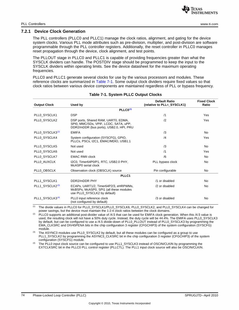
PLL Controllers www.ti.com
7.2.1 Device Clock Generation
The PLL controllers (PLLC0 and PLLC1) manage the clock ratios, alignment, and gating for the devicesystem clocks. Various PLL mode attributes such as pre-division, multiplier, and post-division are softwareprogrammable through the PLL controller registers. Additionally, the reset controller in PLLC0 managesreset propagation through the device, clock alignment, and test points.
The PLLOUT stage in PLLC0 and PLLC1 is capable of providing frequencies greater than what theSYSCLK dividers can handle. The POSTDIV stage should be programmed to keep the input to theSYSCLK dividers within operating limits. See the device datasheet for the maximum operatingfrequencies.
PLLC0 and PLLC1 generate several clocks for use by the various processors and modules. Thesereference clocks are summarized in Table 7-1. Some output clock dividers require fixed values so thatclock ratios between various device components are maintained regardless of PLL or bypass frequency.
Table 7-1. System PLLC Output Clocks
Default Ratio Fixed ClockOutput Clock Used by (relative to PLLn_SYSCLK1) Ratio
PLLC0 (1)
PLL0_SYSCLK1 DSP /1 Yes
PLL0_SYSCLK2 DSP ports, Shared RAM, UART0, EDMA, /2 YesSPI0, MMC/SDs, VPIF, LCDC, SATA, uPP,DDR2/mDDR (bus ports), USB2.0, HPI, PRU
PLL0_SYSCLK3 (2) EMIFA /3 No
PLL0_SYSCLK4 System configuration (SYSCFG), GPIO, /4 YesPLLCs, PSCs, I2C1, EMAC/MDIO, USB1.1
PLL0_SYSCLK5 Not used /3 No
PLL0_SYSCLK6 Not used /1 Yes
PLL0_SYSCLK7 EMAC RMII clock /6 No
PLL0_AUXCLK I2C0, Timer64P0/P1, RTC, USB2.0 PHY, PLL bypass clock NoMcASP0 serial clock
PLL0_OBSCLK Observation clock (OBSCLK) source Pin configurable No
PLLC1
PLL1_SYSCLK1 DDR2/mDDR PHY /1 or disabled No
PLL1_SYSCLK2 (3) ECAPs, UART1/2, Timer64P2/3, eHRPWMs, /2 or disabled NoMcBSPs, McASP0, SPI1 (all these modulesuse PLL0_SYSCLK2 by default)
PLL1_SYSCLK3 (4) PLL0 input reference clock /3 or disabled No(not configured by default)
(1) The divide values in PLLC0 for PLL0_SYSCLK1/PLL0_SYSCLK6, PLL0_SYSCLK2, and PLL0_SYSCLK4 can be changed forpower savings, but the device must maintain the 1:2:4 clock ratios between the clock domains.
(2) PLLC0 supports an additional post-divider value of /4.5 that can be used for EMIFA clock generation. When this /4.5 value isused, the resulting clock will not have a 50% duty cycle. Instead, the duty cycle will be 44.4%. The EMIFA uses PLL0_SYSCLK3by default, but can be configured to use a /4.5 divide-down of PLL0_PLLOUT instead of PLL0_SYSCLK3 by programming theEMA_CLKSRC and DIV45PENA bits in the chip configuration 3 register (CFGCHIP3) of the system configuration (SYSCFG)module.
(3) The ASYNC3 modules use PLL0_SYSCLK2 by default, but all these modules can be configured as a group to usePLL1_SYSCLK2 by programming the ASYNC3_CLKSRC bit in the chip configuration 3 register (CFGCHIP3) of the systemconfiguration (SYSCFG) module.
(4) The PLL0 input clock source can be configured to use PLL1_SYSCLK3 instead of OSCIN/CLKIN by programming theEXTCLKSRC bit in the PLLC0 PLL control register (PLLCTL). The PLL1 input clock source will also be OSCIN/CLKIN.
74 Phase-Locked Loop Controller (PLLC) SPRUGJ7D–April 2010
Copyright © 2010, Texas Instruments Incorporated

www.ti.com PLL Controllers
7.2.2 Steps for Programming the PLLs
Note that there is a lock mechanism implemented to protect the PLL controller registers. SeeSection 7.2.2.1 for information on unlocking the PLL controller registers.
Refer to the appropriate subsection on how to program the PLL clocks:
• If the PLL is powered down (PLLPWRDN bit in PLLCTL is set to 1), follow the full PLL initializationprocedure in Section 7.2.2.2.
• If the PLL is not powered down (PLLPWRDN bit in PLLCTL is cleared to 0), follow the sequence inSection 7.2.2.3 to change the PLL multiplier.
• If the PLL is already running at a desired multiplier and only the SYSCLK dividers will be updated,follow the sequence in Section 7.2.2.4.
Note that the PLLs are powered down after any of the following device-level global resets are asserted:
• Power-on Reset (POR)• Warm Reset (RESET)• Max Reset
7.2.2.1 Locking/Unlocking PLL Register Access
A lock mechanism is implemented on the device to prevent inadvertent writes to the PLL controllerregisters. This provides protection from stopping modules when the module clocks are disabled. Forexample, the watchdog timer that runs on the PLL0_AUXCLK will stop if this PLL clock is unintentionallydisabled.
The PLL lock bits are located within the system configuration (SYSCFG) module:• When set, the PLL_MASTER_LOCK bit in the chip configuration 0 register (CFGCHIP0) locks PLLC0.• When set, the PLL1_MASTER_LOCK bit in the chip configuration 3 register (CFGCHIP3) locks PLLC1.
Because the SYSCFG module has its own lock mechanism, the SYSCFG module must be unlocked firstby writing to the KICK0R and KICK1R registers before the PLL lock bits can be cleared. Like the KICKregisters, the PLL lock bits can only be modified while in a privileged mode. See Chapter 10 forinformation on privilege type and the KICK0R and KICK1R registers.
NOTE: The PLL_MASTER_LOCK bit in CFGCHIP0 and the PLL1_MASTER_LOCK bit inCFGCHIP3 default to unlocked after reset, so the following procedure is only required if thePLLs have been locked (set to 1).
To modify the PLL controller registers, use the following sequence:
1. Write the correct key values to KICK0R and KICK1R registers.2. Clear the PLL_MASTER_LOCK bit in CFGCHIP0 and/or the PLL1_MASTER_LOCK bit in CFGCHIP3,
as required.3. Configure the desired PLL controller register values.4. Set the PLL_MASTER_LOCK bit in CFGCHIP0 and/or the PLL1_MASTER_LOCK bit in CFGCHIP3,
as required.5. Write an incorrect key value to the KICK0R and KICK1R registers.
75SPRUGJ7D–April 2010 Phase-Locked Loop Controller (PLLC)
Copyright © 2010, Texas Instruments Incorporated

PLL Controllers www.ti.com
7.2.2.2 Initializing PLL Mode from PLL Power Down
If the PLL is powered down (PLLPWRDN bit in PLLCTL is set to 1), perform the following procedure toinitialize the PLL:
1. Program the CLKMODE bit in PLLC0 PLLCTL.2. Switch the PLL to bypass mode:
(a) Clear the PLLENSRC bit in PLLCTL to 0 (allows PLLEN bit to take effect).(b) For PLL0 only, select the clock source by programming the EXTCLKSRC bit in PLLCTL.(c) Clear the PLLEN bit in PLLCTL to 0 (PLL in bypass mode).(d) Wait for 4 OSCIN cycles to ensure that the PLLC has switched to bypass mode.
3. Clear the PLLRST bit in PLLCTL to 0 (resets PLL).4. Clear the PLLPWRDN bit in PLLCTL to 0 (brings PLL out of power-down mode).5. Program the desired multiplier value in PLLM. Program the POSTDIV, as needed.6. If desired, program PLLDIVn registers to change the SYSCLKn divide values:
(a) Wait for the GOSTAT bit in PLLSTAT to clear to 0 (indicates that no operation is currently inprogress).
(b) Program the RATIO field in PLLDIVn.(c) Set the GOSET bit in PLLCMD to 1 (initiates a new divider transition).(d) Wait for the GOSTAT bit in PLLSTAT to clear to 0 (completion of divider change).
7. Set the PLLRST bit in PLLCTL to 1 (brings PLL out of reset).8. Wait for the PLL to lock. See the device-specific data manual for PLL lock time.9. Set the PLLEN bit in PLLCTL to 1 (removes PLL from bypass mode).
7.2.2.3 Changing PLL Multiplier
If the PLL is not powered down (PLLPWRDN bit in PLLCTL is cleared to 0), perform the followingprocedure to change the PLL multiplier:
1. Switch the PLL to bypass mode:
(a) Clear the PLLENSRC bit in PLLCTL to 0 (allows PLLEN bit to take effect).(b) For PLL0 only, select the clock source by programming the EXTCLKSRC bit in PLLCTL.(c) Clear the PLLEN bit in PLLCTL to 0 (PLL in bypass mode).(d) Wait for 4 OSCIN cycles to ensure that the PLLC has switched to bypass mode.
2. Clear the PLLRST bit in PLLCTL to 0 (resets PLL).3. Program the desired multiplier value in PLLM. Program the POSTDIV, as needed.4. If desired, program PLLDIVn registers to change the SYSCLKn divide values:
(a) Wait for the GOSTAT bit in PLLSTAT to clear to 0 (indicates that no operation is currently inprogress).
(b) Program the RATIO field in PLLDIVn.(c) Set the GOSET bit in PLLCMD to 1 (initiates a new divider transition).(d) Wait for the GOSTAT bit in PLLSTAT to clear to 0 (completion of divider change).
5. Set the PLLRST bit in PLLCTL to 1 (brings PLL out of reset).6. Wait for the PLL to lock. See the device-specific data manual for PLL lock time.7. Set the PLLEN bit in PLLCTL to 1 (removes PLL from bypass mode).
76 Phase-Locked Loop Controller (PLLC) SPRUGJ7D–April 2010
Copyright © 2010, Texas Instruments Incorporated

www.ti.com PLLC Registers
7.2.2.4 Changing SYSCLK Dividers
If the PLL is already operating at the desired multiplier mode, perform the following procedure to changethe SYSCLK divider values:
1. Wait for the GOSTAT bit in PLLSTAT to clear to 0 (indicates that no operation is currently in progress).2. Program the RATIO field in PLLDIVn.3. Set the GOSET bit in PLLCMD to 1 (initiates a new divider transition).4. Wait for the GOSTAT bit in PLLSTAT to clear to 0 (completion of divider change).
7.3 PLLC Registers
Table 7-2 lists the memory-mapped registers for the PLLC0 and Table 7-3 lists the memory-mappedregisters for the PLLC1.
Table 7-2. PLL Controller 0 (PLLC0) Registers
Address Acronym Register Description Section
01C1 1000h REVID PLLC0 Revision Identification Register Section 7.3.1
01C1 10E4h RSTYPE PLLC0 Reset Type Status Register Section 7.3.3
01C1 1100h PLLCTL PLLC0 Control Register Section 7.3.4
01C1 1104h OCSEL PLLC0 OBSCLK Select Register Section 7.3.6
01C1 1110h PLLM PLLC0 PLL Multiplier Control Register Section 7.3.8
01C1 1114h PREDIV PLLC0 Pre-Divider Control Register Section 7.3.9
01C1 1118h PLLDIV1 PLLC0 Divider 1 Register Section 7.3.10
01C1 111Ch PLLDIV2 PLLC0 Divider 2 Register Section 7.3.12
01C1 1120h PLLDIV3 PLLC0 Divider 3 Register Section 7.3.14
01C1 1124h OSCDIV PLLC0 Oscillator Divider 1 Register Section 7.3.20
01C1 1128h POSTDIV PLLC0 PLL Post-Divider Control Register Section 7.3.22
01C1 1138h PLLCMD PLLC0 PLL Controller Command Register Section 7.3.23
01C1 113Ch PLLSTAT PLLC0 PLL Controller Status Register Section 7.3.24
01C1 1140h ALNCTL PLLC0 Clock Align Control Register Section 7.3.25
01C1 1144h DCHANGE PLLC0 PLLDIV Ratio Change Status Register Section 7.3.27
01C1 1148h CKEN PLLC0 Clock Enable Control Register Section 7.3.29
01C1 114Ch CKSTAT PLLC0 Clock Status Register Section 7.3.30
01C1 1150h SYSTAT PLLC0 SYSCLK Status Register Section 7.3.31
01C1 1160h PLLDIV4 PLLC0 Divider 4 Register Section 7.3.16
01C1 1164h PLLDIV5 PLLC0 Divider 5 Register Section 7.3.17
01C1 1168h PLLDIV6 PLLC0 Divider 6 Register Section 7.3.18
01C1 116Ch PLLDIV7 PLLC0 Divider 7 Register Section 7.3.19
01C1 11F0h EMUCNT0 PLLC0 Emulation Performance Counter 0 Register Section 7.3.33
01C1 11F4h EMUCNT1 PLLC0 Emulation Performance Counter 1 Register Section 7.3.34
77SPRUGJ7D–April 2010 Phase-Locked Loop Controller (PLLC)
Copyright © 2010, Texas Instruments Incorporated

PLLC Registers www.ti.com
Table 7-3. PLL Controller 1 (PLLC1) Registers
Address Acronym Register Description Section
01E1 A000h REVID PLLC1 Revision Identification Register Section 7.3.2
01E1 A100h PLLCTL PLLC1 Control Register Section 7.3.5
01E1 A104h OCSEL PLLC1 OBSCLK Select Register Section 7.3.7
01E1 A110h PLLM PLLC1 PLL Multiplier Control Register Section 7.3.8
01E1 A118h PLLDIV1 PLLC1 Divider 1 Register Section 7.3.11
01E1 A11Ch PLLDIV2 PLLC1 Divider 2 Register Section 7.3.13
01E1 A120h PLLDIV3 PLLC1 Divider 3 Register Section 7.3.15
01E1 A124h OSCDIV PLLC1 Oscillator Divider 1 Register Section 7.3.21
01E1 A128h POSTDIV PLLC1 PLL Post-Divider Control Register Section 7.3.22
01E1 A138h PLLCMD PLLC1 PLL Controller Command Register Section 7.3.23
01E1 A13Ch PLLSTAT PLLC1 PLL Controller Status Register Section 7.3.24
01E1 A140h ALNCTL PLLC1 Clock Align Control Register Section 7.3.26
01E1 A144h DCHANGE PLLC1 PLLDIV Ratio Change Status Register Section 7.3.28
01E1 A150h SYSTAT PLLC1 SYSCLK Status Register Section 7.3.32
01E1 A1F0h EMUCNT0 PLLC1 Emulation Performance Counter 0 Register Section 7.3.33
01E1 A1F4h EMUCNT1 PLLC1 Emulation Performance Counter 1 Register Section 7.3.34
7.3.1 PLLC0 Revision Identification Register (REVID)
The PLLC0 revision identification register (REVID) is shown in Figure 7-2 and described in Table 7-4.
Figure 7-2. PLLC0 Revision Identification Register (REVID)31 0
REV
R-4481 3C00h
LEGEND: R = Read only; -n = value after reset
Table 7-4. PLLC0 Revision Identification Register (REVID) Field Descriptions
Bit Field Value Description
31-0 REV 4481 3C00h Peripheral revision ID for PLLC0.
78 Phase-Locked Loop Controller (PLLC) SPRUGJ7D–April 2010
Copyright © 2010, Texas Instruments Incorporated

www.ti.com PLLC Registers
7.3.2 PLLC1 Revision Identification Register (REVID)
The PLLC1 revision identification register (REVID) is shown in Figure 7-3 and described in Table 7-5.
Figure 7-3. PLLC1 Revision Identification Register (REVID)31 0
REV
R-4481 4400h
LEGEND: R = Read only; -n = value after reset
Table 7-5. PLLC1 Revision Identification Register (REVID) Field Descriptions
Bit Field Value Description
31-0 REV 4481 4400h Peripheral revision ID for PLLC1.
7.3.3 Reset Type Status Register (RSTYPE)
The reset type status register (RSTYPE) latches the cause of the last reset. If multiple reset sources areasserted simultaneously, RSTYPE records the reset source that deasserts last. If multiple reset sourcesare asserted and deasserted simultaneously, RSTYPE latches the highest priority reset source. RSTYPEis shown in Figure 7-4 and described in Table 7-6.
Figure 7-4. Reset Type Status Register (RSTYPE)31 16
Reserved
R-0
15 3 2 1 0
Reserved PLLSWRST XWRST POR
R-0 R-0 R-0 R-0
LEGEND: R = Read only; -n = value after reset
Table 7-6. Reset Type Status Register (RSTYPE) Field Descriptions
Bit Field Value Description
31-3 Reserved 0 Reserved
2 PLLSWRST PLL software reset.
0 PLL soft reset was not the last reset to occur.
1 PLL soft was the last reset to occur.
1 XWRST External warm reset.
0 External warm reset was not the last reset to occur.
1 External warm reset was the last reset to occur.
0 POR Power on reset.
0 Power On Reset (POR) was not the last reset to occur.
1 Power On Reset (POR) was the last reset to occur.
79SPRUGJ7D–April 2010 Phase-Locked Loop Controller (PLLC)
Copyright © 2010, Texas Instruments Incorporated

PLLC Registers www.ti.com
7.3.4 PLLC0 Control Register (PLLCTL)
The PLLC0 control register (PLLCTL) is shown in Figure 7-5 and described in Table 7-7.
Figure 7-5. PLLC0 Control Register (PLLCTL)31 16
Reserved
R-0
15 10 9 8
Reserved EXTCLKSRC CLKMODE
R-0 R/W-0 R/W-0
7 6 5 4 3 2 1 0
Reserved PLLENSRC Reserved PLLRST Reserved PLLPWRDN PLLEN
R-1 R/W-1 R/W-1 R/W-0 R-0 R/W-1 R/W-0
LEGEND: R/W = Read/Write; R = Read only; -n = value after reset
Table 7-7. PLLC0 Control Register (PLLCTL) Field Descriptions
Bit Field Value Description
31-10 Reserved 0 Reserved
9 EXTCLKSRC External clock source selection.
0 Use OSCIN for the PLL bypass clock.
1 Use PLL1_SYSCLK3 for the PLL bypass clock.
8 CLKMODE Reference clock selection.
0 Internal oscillator (crystal)
1 Square wave
7-6 Reserved 1 Reserved
5 PLLENSRC 0 This bit must be cleared before the PLLEN bit will have any effect.
4 Reserved 1 Reserved. Write the default value when modifying this register.
3 PLLRST PLL0 reset.
0 PLL0 reset is asserted.
1 PLL0 reset is not asserted.
2 Reserved 0 Reserved
1 PLLPWRDN PLL0 power-down.
0 PLL0 is operating.
1 PLL0 is powered-down.
0 PLLEN PLL0 mode enables.
0 PLL0 is in bypass mode.
1 PLL0 mode is enabled, not bypassed.
80 Phase-Locked Loop Controller (PLLC) SPRUGJ7D–April 2010
Copyright © 2010, Texas Instruments Incorporated

www.ti.com PLLC Registers
7.3.5 PLLC1 Control Register (PLLCTL)
The PLLC1 control register (PLLCTL) is shown in Figure 7-6 and described in Table 7-8.
Figure 7-6. PLLC1 Control Register (PLLCTL)31 16
Reserved
R-0
15 8
Reserved
R-0
7 6 5 4 3 2 1 0
Reserved PLLENSRC Reserved PLLRST Reserved PLLPWRDN PLLEN
R-1 R/W-1 R/W-1 R/W-0 R-0 R/W-1 R/W-0
LEGEND: R/W = Read/Write; R = Read only; -n = value after reset
Table 7-8. PLLC1 Control Register (PLLCTL) Field Descriptions
Bit Field Value Description
31-8 Reserved 0 Reserved
7-6 Reserved 1 Reserved
5 PLLENSRC 0 This bit must be cleared before the PLLEN bit will have any effect.
4 Reserved 1 Reserved. Write the default value when modifying this register.
3 PLLRST PLL1 reset.
0 PLL1 reset is asserted.
1 PLL1 reset is not asserted.
2 Reserved 0 Reserved
1 PLLPWRDN PLL1 power-down.
0 PLL1 is operating.
1 PLL1 is powered-down.
0 PLLEN PLL1 mode enables.
0 PLL1 is in bypass mode.
1 PLL1 mode is enabled, not bypassed.
81SPRUGJ7D–April 2010 Phase-Locked Loop Controller (PLLC)
Copyright © 2010, Texas Instruments Incorporated

PLLC Registers www.ti.com
7.3.6 PLLC0 OBSCLK Select Register (OCSEL)
The PLLC0 OBSCLK select register (OCSEL) controls which clock is output on the CLKOUT pin so that itmay be used for test and debug purposes (in addition to its normal function of being a direct input clockdivider). The OCSEL is shown in Figure 7-7 and described in Table 7-9.
Figure 7-7. PLLC0 OBSCLK Select Register (OCSEL)31 16
Reserved
R-0
15 5 4 0
Reserved OCSRC
R-0 R/W-14h
LEGEND: R/W = Read/Write; R = Read only; -n = value after reset
Table 7-9. PLLC0 OBSCLK Select Register (OCSEL) Field Descriptions
Bit Field Value Description
31-5 Reserved 0 Reserved
4-0 OCSRC 0-1Fh PLLC0 OBSCLK source. Output on CLKOUT pin.
0-13h Reserved
14h OSCIN
15h-16h Reserved
17h PLL0_SYSCLK1
18h PLL0_SYSCLK2
19h PLL0_SYSCLK3
1Ah PLL0_SYSCLK4
1Bh PLL0_SYSCLK5
1Ch PLL0_SYSCLK6
1Dh PLL0_SYSCLK7
1Eh PLLC1 OBSCLK
1Fh Disabled
82 Phase-Locked Loop Controller (PLLC) SPRUGJ7D–April 2010
Copyright © 2010, Texas Instruments Incorporated

www.ti.com PLLC Registers
7.3.7 PLLC1 OBSCLK Select Register (OCSEL)
The PLLC1 OBSCLK select register (OCSEL) controls which clock is output on PLLC1 OBSCLK so that itmay be used for test and debug purposes (in addition to its normal function of being a direct input clockdivider). The OCSEL is shown in Figure 7-8 and described in Table 7-10.
Figure 7-8. PLLC1 OBSCLK Select Register (OCSEL)31 16
Reserved
R-0
15 5 4 0
Reserved OCSRC
R-0 R/W-14h
LEGEND: R/W = Read/Write; R = Read only; -n = value after reset
Table 7-10. PLLC1 OBSCLK Select Register (OCSEL) Field Descriptions
Bit Field Value Description
31-5 Reserved 0 Reserved
4-0 OCSRC 0-1Fh PLLC1 OBSCLK source.
0-13h Reserved
14h OSCIN
15h-16h Reserved
17h PLL1_SYSCLK1
18h PLL1_SYSCLK2
19h PLL1_SYSCLK3
1A-1Fh Reserved
83SPRUGJ7D–April 2010 Phase-Locked Loop Controller (PLLC)
Copyright © 2010, Texas Instruments Incorporated

PLLC Registers www.ti.com
7.3.8 PLL Multiplier Control Register (PLLM)
The PLL multiplier control register (PLLM) is shown in Figure 7-9 and described in Table 7-11.
Figure 7-9. PLL Multiplier Control Register (PLLM)31 16
Reserved
R-0
15 5 4 0
Reserved PLLM
R-0 R/W-13h
LEGEND: R/W = Read/Write; R = Read only; -n = value after reset
Table 7-11. PLL Multiplier Control Register (PLLM) Field Descriptions
Bit Field Value Description
31-5 Reserved 0 Reserved
4-0 PLLM 0-1Fh PLL multiplier select. Multiplier Value = PLLM + 1. The valid range of multiplier values for a givenMXI/CLKIN is defined by the minimum and maximum frequency limits on the PLL VCO frequency. Seethe device-specific data manual for PLL VCO frequency specification limits.
7.3.9 PLLC0 Pre-Divider Control Register (PREDIV)
The PLLC0 pre-divider control register (PREDIV) is shown in Figure 7-10 and described in Table 7-12.
Figure 7-10. PLLC0 Pre-Divider Control Register (PREDIV)31 16
Reserved
R-0
15 14 5 4 0
PREDEN Reserved RATIO
R/W-1 R-0 R/W-0
LEGEND: R/W = Read/Write; R = Read only; -n = value after reset
Table 7-12. PLLC0 Pre-Divider Control Register (PREDIV) Field Descriptions
Bit Field Value Description
31-14 Reserved 0 Reserved
15 PREDEN PLLC0 pre-divider enable.
0 PLLC0 pre-divider is disabled.
1 PLLC0 pre-divider is enabled.
14-5 Reserved 0 Reserved
4-0 RATIO 0-1Fh Divider ratio. Divider Value = RATIO + 1. RATIO defaults to 0 (PLL pre-divide by 1).
84 Phase-Locked Loop Controller (PLLC) SPRUGJ7D–April 2010
Copyright © 2010, Texas Instruments Incorporated

www.ti.com PLLC Registers
7.3.10 PLLC0 Divider 1 Register (PLLDIV1)
The PLLC0 divider 1 register (PLLDIV1) controls the divider for PLL0_SYSCLK1. PLLDIV1 is shown inFigure 7-11 and described in Table 7-13.
Figure 7-11. PLLC0 Divider 1 Register (PLLDIV1)31 16
Reserved
R-0
15 14 5 4 0
D1EN Reserved RATIO
R/W-1 R-0 R/W-0
LEGEND: R/W = Read/Write; R = Read only; -n = value after reset
Table 7-13. PLLC0 Divider 1 Register (PLLDIV1) Field Descriptions
Bit Field Value Description
31-16 Reserved 0 Reserved
15 D1EN Divider 1 enable.
0 Divider 1 is disabled.
1 Divider 1 is enabled.
14-5 Reserved 0 Reserved
4-0 RATIO 0-1Fh Divider ratio. Divider Value = RATIO + 1. RATIO defaults to 0 (PLL divide by 1).
7.3.11 PLLC1 Divider 1 Register (PLLDIV1)
The PLLC1 divider 1 register (PLLDIV1) controls the divider for PLL1_SYSCLK1. PLLDIV1 is shown inFigure 7-12 and described in Table 7-14.
Figure 7-12. PLLC1 Divider 1 Register (PLLDIV1)31 16
Reserved
R-0
15 14 5 4 0
D1EN Reserved RATIO
R/W-0 R-0 R/W-0
LEGEND: R/W = Read/Write; R = Read only; -n = value after reset
Table 7-14. PLLC1 Divider 1 Register (PLLDIV1) Field Descriptions
Bit Field Value Description
31-16 Reserved 0 Reserved
15 D1EN Divider 1 enable.
0 Divider 1 is disabled.
1 Divider 1 is enabled.
14-5 Reserved 0 Reserved
4-0 RATIO 0-1Fh Divider ratio. Divider Value = RATIO + 1. RATIO defaults to 0 (PLL divide by 1).
85SPRUGJ7D–April 2010 Phase-Locked Loop Controller (PLLC)
Copyright © 2010, Texas Instruments Incorporated

PLLC Registers www.ti.com
7.3.12 PLLC0 Divider 2 Register (PLLDIV2)
The PLLC0 divider 2 register (PLLDIV2) controls the divider for PLL0_SYSCLK2. PLLDIV2 is shown inFigure 7-13 and described in Table 7-15.
Figure 7-13. PLLC0 Divider 2 Register (PLLDIV2)31 16
Reserved
R-0
15 14 5 4 0
D2EN Reserved RATIO
R/W-1 R-0 R/W-1
LEGEND: R/W = Read/Write; R = Read only; -n = value after reset
Table 7-15. PLLC0 Divider 2 Register (PLLDIV2) Field Descriptions
Bit Field Value Description
31-16 Reserved 0 Reserved
15 D2EN Divider 2 enable.
0 Divider 2 is disabled.
1 Divider 2 is enabled.
14-5 Reserved 0 Reserved
4-0 RATIO 0-1Fh Divider ratio. Divider Value = RATIO + 1. RATIO defaults to 1 (PLL divide by 2).
7.3.13 PLLC1 Divider 2 Register (PLLDIV2)
The PLLC1 divider 2 register (PLLDIV2) controls the divider for PLL1_SYSCLK2. PLLDIV2 is shown inFigure 7-14 and described in Table 7-16.
Figure 7-14. PLLC1 Divider 2 Register (PLLDIV2)31 16
Reserved
R-0
15 14 5 4 0
D2EN Reserved RATIO
R/W-0 R-0 R/W-1
LEGEND: R/W = Read/Write; R = Read only; -n = value after reset
Table 7-16. PLLC1 Divider 2 Register (PLLDIV2) Field Descriptions
Bit Field Value Description
31-16 Reserved 0 Reserved
15 D2EN Divider 2 enable.
0 Divider 2 is disabled.
1 Divider 2 is enabled.
14-5 Reserved 0 Reserved
4-0 RATIO 0-1Fh Divider ratio. Divider Value = RATIO + 1. RATIO defaults to 1 (PLL divide by 2).
86 Phase-Locked Loop Controller (PLLC) SPRUGJ7D–April 2010
Copyright © 2010, Texas Instruments Incorporated
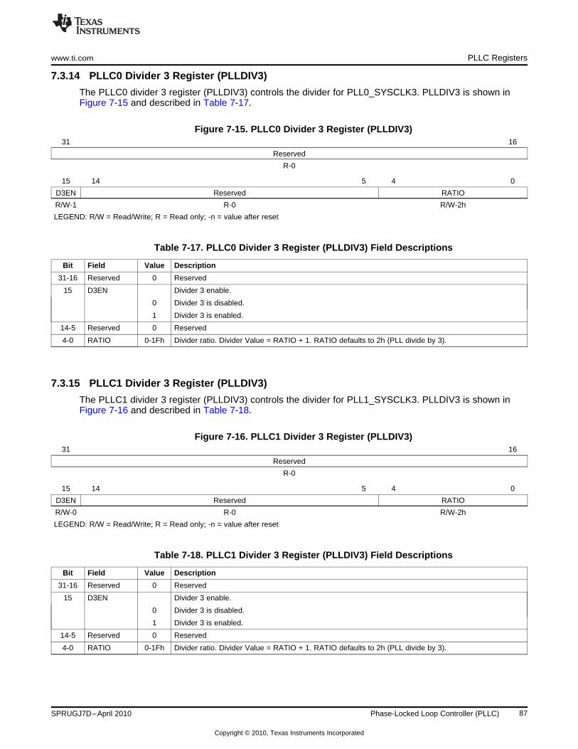
www.ti.com PLLC Registers
7.3.14 PLLC0 Divider 3 Register (PLLDIV3)
The PLLC0 divider 3 register (PLLDIV3) controls the divider for PLL0_SYSCLK3. PLLDIV3 is shown inFigure 7-15 and described in Table 7-17.
Figure 7-15. PLLC0 Divider 3 Register (PLLDIV3)31 16
Reserved
R-0
15 14 5 4 0
D3EN Reserved RATIO
R/W-1 R-0 R/W-2h
LEGEND: R/W = Read/Write; R = Read only; -n = value after reset
Table 7-17. PLLC0 Divider 3 Register (PLLDIV3) Field Descriptions
Bit Field Value Description
31-16 Reserved 0 Reserved
15 D3EN Divider 3 enable.
0 Divider 3 is disabled.
1 Divider 3 is enabled.
14-5 Reserved 0 Reserved
4-0 RATIO 0-1Fh Divider ratio. Divider Value = RATIO + 1. RATIO defaults to 2h (PLL divide by 3).
7.3.15 PLLC1 Divider 3 Register (PLLDIV3)
The PLLC1 divider 3 register (PLLDIV3) controls the divider for PLL1_SYSCLK3. PLLDIV3 is shown inFigure 7-16 and described in Table 7-18.
Figure 7-16. PLLC1 Divider 3 Register (PLLDIV3)31 16
Reserved
R-0
15 14 5 4 0
D3EN Reserved RATIO
R/W-0 R-0 R/W-2h
LEGEND: R/W = Read/Write; R = Read only; -n = value after reset
Table 7-18. PLLC1 Divider 3 Register (PLLDIV3) Field Descriptions
Bit Field Value Description
31-16 Reserved 0 Reserved
15 D3EN Divider 3 enable.
0 Divider 3 is disabled.
1 Divider 3 is enabled.
14-5 Reserved 0 Reserved
4-0 RATIO 0-1Fh Divider ratio. Divider Value = RATIO + 1. RATIO defaults to 2h (PLL divide by 3).
87SPRUGJ7D–April 2010 Phase-Locked Loop Controller (PLLC)
Copyright © 2010, Texas Instruments Incorporated

PLLC Registers www.ti.com
7.3.16 PLLC0 Divider 4 Register (PLLDIV4)
The PLLC0 divider 4 register (PLLDIV4) controls the divider for PLL0_SYSCLK4. PLLDIV4 is showninFigure 7-17 and described in Table 7-19.
Figure 7-17. PLLC0 Divider 4 Register (PLLDIV4)31 16
Reserved
R-0
15 14 5 4 0
D4EN Reserved RATIO
R/W-1 R-0 R/W-3h
LEGEND: R/W = Read/Write; R = Read only; -n = value after reset
Table 7-19. PLLC0 Divider 4 Register (PLLDIV4) Field Descriptions
Bit Field Value Description
31-16 Reserved 0 Reserved
15 D4EN Divider 4 enable.
0 Divider 4 is disabled.
1 Divider 4 is enabled.
14-5 Reserved 0 Reserved
4-0 RATIO 0-1Fh Divider ratio. Divider Value = RATIO + 1. RATIO defaults 3 (PLL divide by 4).
7.3.17 PLLC0 Divider 5 Register (PLLDIV5)
The PLLC0 divider 5 register (PLLDIV5) controls the divider for PLL0_SYSCLK5. PLLDIV5 is shown inFigure 7-18 and described in Table 7-20.
Figure 7-18. PLLC0 Divider 5 Register (PLLDIV5)31 16
Reserved
R-0
15 14 5 4 0
D5EN Reserved RATIO
R/W-1 R-0 R/W-2h
LEGEND: R/W = Read/Write; R = Read only; -n = value after reset
Table 7-20. PLLC0 Divider 5 Register (PLLDIV5) Field Descriptions
Bit Field Value Description
31-16 Reserved 0 Reserved
15 D5EN Divider 5 enable.
0 Divider 5 is disabled.
1 Divider 5 is enabled.
14-5 Reserved 0 Reserved
4-0 RATIO 0-1Fh Divider ratio. Divider Value = RATIO + 1. RATIO defaults 2 (PLL divide by 3).
88 Phase-Locked Loop Controller (PLLC) SPRUGJ7D–April 2010
Copyright © 2010, Texas Instruments Incorporated

www.ti.com PLLC Registers
7.3.18 PLLC0 Divider 6 Register (PLLDIV6)
The PLLC0 divider 6 register (PLLDIV6) controls the divider for PLL0_SYSCLK6. PLLDIV6 is shown inFigure 7-19 and described in Table 7-21.
Figure 7-19. PLLC0 Divider 6 Register (PLLDIV6)31 16
Reserved
R-0
15 14 5 4 0
D6EN Reserved RATIO
R/W-1 R-0 R/W-0
LEGEND: R/W = Read/Write; R = Read only; -n = value after reset
Table 7-21. PLLC0 Divider 6 Register (PLLDIV6) Field Descriptions
Bit Field Value Description
31-16 Reserved 0 Reserved
15 D6EN Divider 6 enable.
0 Divider 6 is disabled.
1 Divider 6 is enabled.
14-5 Reserved 0 Reserved
4-0 RATIO 0-1Fh Divider ratio. Divider Value = RATIO + 1. RATIO defaults to 0 (PLL divide by 1).
7.3.19 PLLC0 Divider 7 Register (PLLDIV7)
The PLLC0 divider 7 register (PLLDIV7) controls the divider for PLL0_SYSCLK7. PLLDIV7 is shown inFigure 7-20 and described in Table 7-22.
Figure 7-20. PLLC0 Divider 7 Register (PLLDIV7)31 16
Reserved
R-0
15 14 5 4 0
D7EN Reserved RATIO
R/W-1 R-0 R/W-5h
LEGEND: R/W = Read/Write; R = Read only; -n = value after reset
Table 7-22. PLLC0 Divider 7 Register (PLLDIV7) Field Descriptions
Bit Field Value Description
31-16 Reserved 0 Reserved
15 D7EN Divider 7 enable.
0 Divider 7 is disabled.
1 Divider 7 is enabled.
14-5 Reserved 0 Reserved
4-0 RATIO 0-1Fh Divider ratio. Divider Value = RATIO + 1. RATIO defaults to 5 (PLL divide by 6).
89SPRUGJ7D–April 2010 Phase-Locked Loop Controller (PLLC)
Copyright © 2010, Texas Instruments Incorporated

PLLC Registers www.ti.com
7.3.20 PLLC0 Oscillator Divider 1 Register (OSCDIV)
The PLLC0 oscillator divider 1 register (OSCDIV) controls the divider for PLLC0 OBSCLK, dividing downthe clock selected as the PLLC0 OBSCLK source. The PLLC0 OBSCLK is connected to the CLKOUT pin.The OSCDIV is shown in Figure 7-21 and described in Table 7-23.
Figure 7-21. PLLC0 Oscillator Divider 1 Register (OSCDIV)31 16
Reserved
R-0
15 14 5 4 0
OD1EN Reserved RATIO
R/W-1 R-0 R/W-0
LEGEND: R/W = Read/Write; R = Read only; -n = value after reset
Table 7-23. PLLC0 Oscillator Divider 1 Register (OSCDIV) Field Descriptions
Bit Field Value Description
31-16 Reserved 0 Reserved
15 OD1EN Oscillator divider 1 enable.
0 Oscillator divider 1 is disabled.
1 Oscillator divider 1 is enabled. For PLLC0 OBSCLK to toggle, both the OD1EN bit and the OBSEN bit inthe clock enable control register (CKEN) must be set to 1.
14-5 Reserved 0 Reserved
4-0 RATIO 0-1Fh Divider ratio. Divider value = RATIO + 1. For example, RATIO = 0 means divide by 1.
7.3.21 PLLC1 Oscillator Divider 1 Register (OSCDIV)
The PLLC1 oscillator divider 1 register (OSCDIV) controls the divider for PLLC1 OBSCLK, dividing downthe clock selected as the PLLC1 OBSCLK source. The PLLC1 OBSCLK signal may be selected as theoutput on the CLKOUT pin. The OSCDIV is shown in Figure 7-22 and described in Table 7-24.
Figure 7-22. PLLC1 Oscillator Divider 1 Register (OSCDIV)31 16
Reserved
R-0
15 14 5 4 0
OD1EN Reserved RATIO
R/W-1 R-0 R/W-0
LEGEND: R/W = Read/Write; R = Read only; -n = value after reset
Table 7-24. PLLC1 Oscillator Divider 1 Register (OSCDIV) Field Descriptions
Bit Field Value Description
31-16 Reserved 0 Reserved
15 OD1EN Oscillator divider 1 enable.
0 Oscillator divider 1 is disabled.
1 Oscillator divider 1 is enabled.
14-5 Reserved 0 Reserved
4-0 RATIO 0-1Fh Divider ratio. Divider value = RATIO + 1. For example, RATIO = 0 means divide by 1.
90 Phase-Locked Loop Controller (PLLC) SPRUGJ7D–April 2010
Copyright © 2010, Texas Instruments Incorporated

www.ti.com PLLC Registers
7.3.22 PLL Post-Divider Control Register (POSTDIV)
The PLL post-divider control register (POSTDIV) is shown in Figure 7-23 and described in Table 7-25.
Figure 7-23. PLL Post-Divider Control Register (POSTDIV)31 16
Reserved
R-0
15 14 5 4 0
POSTDEN Reserved RATIO
R/W-1 R-0 R/W-1
LEGEND: R/W = Read/Write; R = Read only; -n = value after reset
Table 7-25. PLL Post-Divider Control Register (POSTDIV) Field Descriptions
Bit Field Value Description
31-16 Reserved 0 Reserved
15 POSTDEN Post-divider enable.
0 Post-divider is disabled.
1 Post-divider is enabled.
14-5 Reserved 0 Reserved
4-0 RATIO 0-1Fh Divider ratio. Divider Value = RATIO + 1. RATIO defaults to 1 (PLL post-divide by 2).
7.3.23 PLL Controller Command Register (PLLCMD)
The PLL controller command register (PLLCMD) contains the command bit for phase alignment. A write of1 initiates the command; a write of 0 clears the bit, but has no effect. PLLCMD is shown in Figure 7-24and described in Table 7-26.
Figure 7-24. PLL Controller Command Register (PLLCMD)31 16
Reserved
R-0
15 1 0
Reserved GOSET
R-0 R/W0C-0
LEGEND: R/W = Read/Write; R = Read only; W0C = Write 0 to clear bit; -n = value after reset
Table 7-26. PLL Controller Command Register (PLLCMD) Field Descriptions
Bit Field Value Description
31-1 Reserved 0 Reserved
0 GOSET GO bit for phase alignment.
0 Clear bit (no effect)
1 Phase alignment
91SPRUGJ7D–April 2010 Phase-Locked Loop Controller (PLLC)
Copyright © 2010, Texas Instruments Incorporated
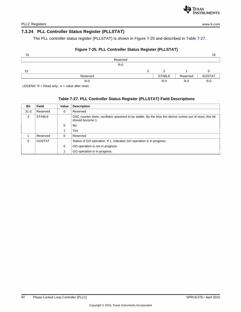
PLLC Registers www.ti.com
7.3.24 PLL Controller Status Register (PLLSTAT)
The PLL controller status register (PLLSTAT) is shown in Figure 7-25 and described in Table 7-27.
Figure 7-25. PLL Controller Status Register (PLLSTAT)31 16
Reserved
R-0
15 3 2 1 0
Reserved STABLE Reserved GOSTAT
R-0 R-0 R-0 R-0
LEGEND: R = Read only; -n = value after reset
Table 7-27. PLL Controller Status Register (PLLSTAT) Field Descriptions
Bit Field Value Description
31-3 Reserved 0 Reserved
2 STABLE OSC counter done, oscillator assumed to be stable. By the time the device comes out of reset, this bitshould become 1.
0 No
1 Yes
1 Reserved 0 Reserved
0 GOSTAT Status of GO operation. If 1, indicates GO operation is in progress.
0 GO operation is not in progress.
1 GO operation is in progress.
92 Phase-Locked Loop Controller (PLLC) SPRUGJ7D–April 2010
Copyright © 2010, Texas Instruments Incorporated

www.ti.com PLLC Registers
7.3.25 PLLC0 Clock Align Control Register (ALNCTL)
The PLLC0 clock align control register (ALNCTL) indicates which PLL0_SYSCLKn needs to be aligned forproper device operation. ALNCTL is shown in Figure 7-26 and described in Table 7-28.
Figure 7-26. PLLC0 Clock Align Control Register (ALNCTL)31 16
Reserved
R-0
15 7 6 5 4 3 2 1 0
Reserved ALN7 ALN6 ALN5 ALN4 ALN3 ALN2 ALN1
R-3h R/W-1 R/W-1 R/W-1 R/W-1 R/W-1 R/W-1 R/W-1
LEGEND: R/W = Read/Write; R = Read only; -n = value after reset
Table 7-28. PLLC0 Clock Align Control Register (ALNCTL) Field Descriptions
Bit Field Value Description
31-7 Reserved 3h Reserved
6 ALN7 PLL0_SYSCLK7 needs to be aligned to others selected in this register.
0 No
1 Yes
5 ALN6 PLL0_SYSCLK6 needs to be aligned to others selected in this register.
0 No
1 Yes
4 ALN5 PLL0_SYSCLK5 needs to be aligned to others selected in this register.
0 No
1 Yes
3 ALN4 PLL0_SYSCLK4 needs to be aligned to others selected in this register.
0 No
1 Yes
2 ALN3 PLL0_SYSCLK3 needs to be aligned to others selected in this register.
0 No
1 Yes
1 ALN2 PLL0_SYSCLK2 needs to be aligned to others selected in this register.
0 No
1 Yes
0 ALN1 PLL0_SYSCLK1 needs to be aligned to others selected in this register.
0 No
1 Yes
93SPRUGJ7D–April 2010 Phase-Locked Loop Controller (PLLC)
Copyright © 2010, Texas Instruments Incorporated
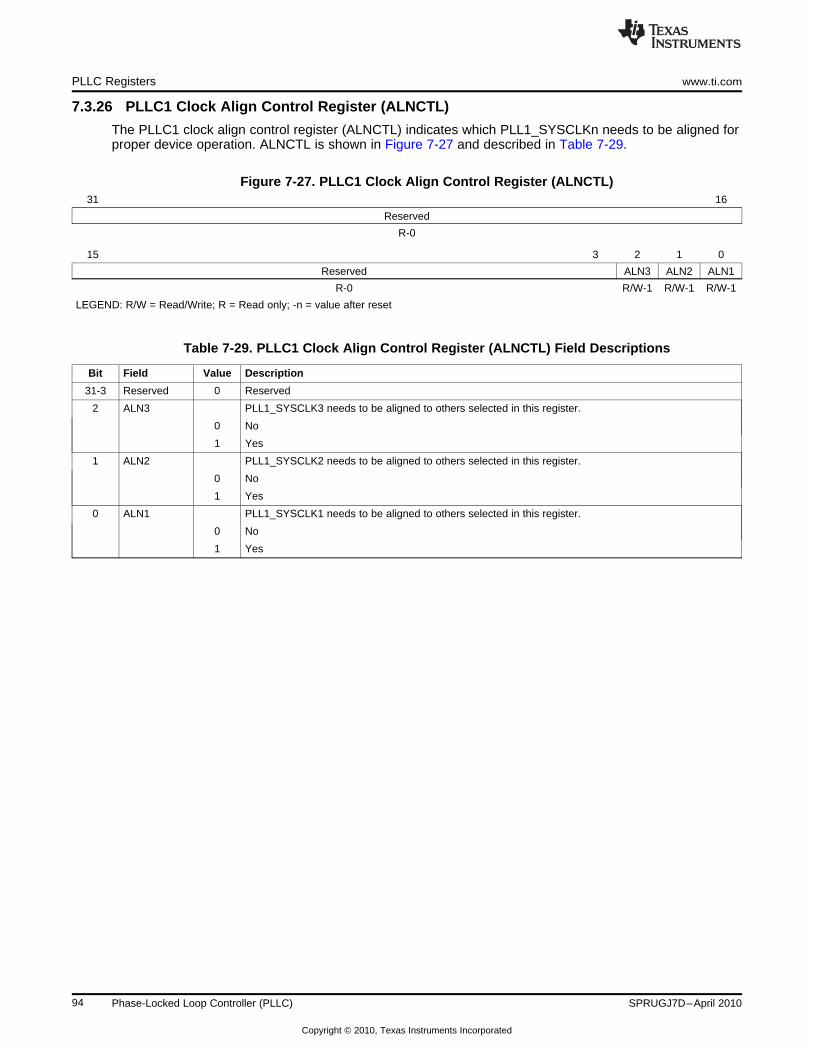
PLLC Registers www.ti.com
7.3.26 PLLC1 Clock Align Control Register (ALNCTL)
The PLLC1 clock align control register (ALNCTL) indicates which PLL1_SYSCLKn needs to be aligned forproper device operation. ALNCTL is shown in Figure 7-27 and described in Table 7-29.
Figure 7-27. PLLC1 Clock Align Control Register (ALNCTL)31 16
Reserved
R-0
15 3 2 1 0
Reserved ALN3 ALN2 ALN1
R-0 R/W-1 R/W-1 R/W-1
LEGEND: R/W = Read/Write; R = Read only; -n = value after reset
Table 7-29. PLLC1 Clock Align Control Register (ALNCTL) Field Descriptions
Bit Field Value Description
31-3 Reserved 0 Reserved
2 ALN3 PLL1_SYSCLK3 needs to be aligned to others selected in this register.
0 No
1 Yes
1 ALN2 PLL1_SYSCLK2 needs to be aligned to others selected in this register.
0 No
1 Yes
0 ALN1 PLL1_SYSCLK1 needs to be aligned to others selected in this register.
0 No
1 Yes
94 Phase-Locked Loop Controller (PLLC) SPRUGJ7D–April 2010
Copyright © 2010, Texas Instruments Incorporated

www.ti.com PLLC Registers
7.3.27 PLLC0 PLLDIV Ratio Change Status Register (DCHANGE)
The PLLC0 PLLDIV ratio change status register (DCHANGE) indicates if the PLL0_SYSCLKn divide ratiohas been modified. DCHANGE is shown in Figure 7-28 and described in Table 7-30.
Figure 7-28. PLLC0 PLLDIV Ratio Change Status Register (DCHANGE)31 16
Reserved
R-0
15 7 6 5 4 3 2 1 0
Reserved SYS7 SYS6 SYS5 SYS4 SYS3 SYS2 SYS1
R-0 R-0 R-0 R-0 R-0 R-0 R-0 R-0
LEGEND: R = Read only; -n = value after reset
Table 7-30. PLLC0 PLLDIV Ratio Change Status Register (DCHANGE) Field Descriptions
Bit Field Value Description
31-7 Reserved 0 Reserved
6 SYS7 PLL0_SYSCLK7 divide ratio is modified.
0 Ratio is not modified.
1 Ratio is modified.
5 SYS6 PLL0_SYSCLK6 divide ratio is modified.
0 Ratio is not modified.
1 Ratio is modified.
4 SYS5 PLL0_SYSCLK5 divide ratio is modified.
0 Ratio is not modified.
1 Ratio is modified.
3 SYS4 PLL0_SYSCLK4 divide ratio is modified.
0 Ratio is not modified.
1 Ratio is modified.
2 SYS3 PLL0_SYSCLK3 divide ratio is modified.
0 Ratio is not modified.
1 Ratio is modified.
1 SYS2 PLL0_SYSCLK2 divide ratio is modified.
0 Ratio is not modified.
1 Ratio is modified.
0 SYS1 PLL0_SYSCLK1 divide ratio is modified.
0 Ratio is not modified.
1 Ratio is modified.
95SPRUGJ7D–April 2010 Phase-Locked Loop Controller (PLLC)
Copyright © 2010, Texas Instruments Incorporated

PLLC Registers www.ti.com
7.3.28 PLLC1 PLLDIV Ratio Change Status Register (DCHANGE)
The PLLC1 PLLDIV ratio change status register (DCHANGE) indicates if the PLL1_SYSCLKn divide ratiohas been modified. DCHANGE is shown in Figure 7-29 and described in Table 7-31.
Figure 7-29. PLLC1 PLLDIV Ratio Change Status Register (DCHANGE)31 16
Reserved
R-0
15 3 2 1 0
Reserved SYS3 SYS2 SYS1
R-0 R-0 R-0 R-0
LEGEND: R = Read only; -n = value after reset
Table 7-31. PLLC1 PLLDIV Ratio Change Status Register (DCHANGE) Field Descriptions
Bit Field Value Description
31-3 Reserved 0 Reserved
2 SYS3 PLL1_SYSCLK3 divide ratio is modified.
0 Ratio is not modified.
1 Ratio is modified.
1 SYS2 PLL1_SYSCLK2 divide ratio is modified.
0 Ratio is not modified.
1 Ratio is modified.
0 SYS1 PLL1_SYSCLK1 divide ratio is modified.
0 Ratio is not modified.
1 Ratio is modified.
96 Phase-Locked Loop Controller (PLLC) SPRUGJ7D–April 2010
Copyright © 2010, Texas Instruments Incorporated

www.ti.com PLLC Registers
7.3.29 PLLC0 Clock Enable Control Register (CKEN)
The PLLC0 clock enable control register (CKEN) controls the PLLC0 OBSCLK and AUXCLK clock. CKENis shown in Figure 7-30 and described in Table 7-32.
Figure 7-30. PLLC0 Clock Enable Control Register (CKEN)31 16
Reserved
R-0
15 2 1 0
Reserved OBSEN AUXEN
R-0 R/W-1 R/W-1
LEGEND: R/W = Read/Write; R = Read only; -n = value after reset
Table 7-32. PLLC0 Clock Enable Control Register (CKEN) Field Descriptions
Bit Field Value Description
31-2 Reserved 0 Reserved
1 OBSEN OBSCLK enable. Actual PLLC0 OBSCLK status is shown in the clock status register (CKSTAT).
0 OBSCLK is disabled.
1 OBSCLK is enabled. For PLLC0 OBSCLK to toggle, both the OBSEN bit and the OD1EN bit in thePLLC0 oscillator divider 1 register (OSCDIV) must be set to 1.
0 AUXEN AUXCLK enable. Actual AUXCLK status is shown in the clock status register (CKSTAT).
0 AUXCLK is disabled.
1 AUXCLK is enabled.
97SPRUGJ7D–April 2010 Phase-Locked Loop Controller (PLLC)
Copyright © 2010, Texas Instruments Incorporated

PLLC Registers www.ti.com
7.3.30 PLLC0 Clock Status Register (CKSTAT)
The PLLC0 clock status register (CKSTAT) indicates the PLLC0 OBSCLK and AUXCLK on/off status. ThePLLn_SYSCLK status is shown in the PLLCn SYSCLK status register (SYSTAT). CKSTAT is shown inFigure 7-31 and described in Table 7-33.
Figure 7-31. PLLC0 Clock Status Register (CKSTAT)31 16
Reserved
R-0
15 1 0
Reserved OBSEN AUXEN
R-0 R-1 R-1
LEGEND: R = Read only; -n = value after reset
Table 7-33. PLLC0 Clock Status Register (CKSTAT) Field Descriptions
Bit Field Value Description
31-2 Reserved 0 Reserved
1 OBSEN OBSCLK on status. PLLC0 OBSCLK is controlled in the PLLC0 oscillator divider 1 register (OSCDIV)by the OBSEN bit in the clock enable control register (CKEN).
0 PLLC0 OBSCLK is off.
1 PLLC0 OBSCLK is on.
0 AUXEN AUXCLK on status. AUXCLK is controlled by the AUXEN bit in the clock enable control register(CKEN).
0 AUXCLK is off.
1 AUXCLK is on.
98 Phase-Locked Loop Controller (PLLC) SPRUGJ7D–April 2010
Copyright © 2010, Texas Instruments Incorporated

www.ti.com PLLC Registers
7.3.31 PLLC0 SYSCLK Status Register (SYSTAT)
The PLLC0 SYSCLK status register (SYSTAT) indicates the PLL0_SYSCLKn on/off status. The actualdefault is determined by the actual clock on/off status, which depends on the DnEN bit in PLLC0 PLLDIVn.SYSTAT is shown in Figure 7-32 and described in Table 7-34.
Figure 7-32. PLLC0 SYSCLK Status Register (SYSTAT)31 8
Reserved
R-1
7 6 5 4 3 2 1 0
Reserved SYS7ON SYS6ON SYS5ON SYS4ON SYS3ON SYS2ON SYS1ON
R-1 R-1 R-1 R-1 R-1 R-1 R-1 R-1
LEGEND: R/W = Read/Write; R = Read only; -n = value after reset
Table 7-34. PLLC0 SYSCLK Status Register (SYSTAT) Field Descriptions
Bit Field Value Description
31-7 Reserved 3h Reserved
6 SYS7ON PLL0_SYSCLK7 on status.
0 Off
1 On
5 SYS6ON PLL0_SYSCLK6 on status.
0 Off
1 On
4 SYS5ON PLL0_SYSCLK5 on status.
0 Off
1 On
3 SYS4ON PLL0_SYSCLK4 on status.
0 Off
1 On
2 SYS3ON PLL0_SYSCLK3 on status.
0 Off
1 On
1 SYS2ON PLL0_SYSCLK2 on status.
0 Off
1 On
0 SYS1ON PLL0_SYSCLK1 on status.
0 Off
1 On
99SPRUGJ7D–April 2010 Phase-Locked Loop Controller (PLLC)
Copyright © 2010, Texas Instruments Incorporated

PLLC Registers www.ti.com
7.3.32 PLLC1 SYSCLK Status Register (SYSTAT)
The PLLC1 SYSCLK status register (SYSTAT) indicates the PLL1_SYSCLKn on/off status. The actualdefault is determined by the actual clock on/off status, which depends on the DnEN bit in PLLC1 PLLDIVn.SYSTAT is shown in Figure 7-33 and described in Table 7-35.
Figure 7-33. PLLC1 SYSCLK Status Register (SYSTAT)31 8
Reserved
R-0
7 3 2 1 0
Reserved SYS3ON SYS2ON SYS1ON
R-0 R-0 R-0 R-0
LEGEND: R/W = Read/Write; R = Read only; -n = value after reset
Table 7-35. PLLC1 SYSCLK Status Register (SYSTAT) Field Descriptions
Bit Field Value Description
31-3 Reserved 0 Reserved
2 SYS3ON PLL1_SYSCLK3 on status.
0 Off
1 On
1 SYS2ON PLL1_SYSCLK2 on status.
0 Off
1 On
0 SYS1ON PLL1_SYSCLK1 on status.
0 Off
1 On
100 Phase-Locked Loop Controller (PLLC) SPRUGJ7D–April 2010
Copyright © 2010, Texas Instruments Incorporated

www.ti.com PLLC Registers
7.3.33 Emulation Performance Counter 0 Register (EMUCNT0)
The emulation performance counter 0 register (EMUCNT0) is shown in Figure 7-34 and described inTable 7-36. EMUCNT0 is for emulation performance profiling. It counts in a divide-by-4 of the systemclock. To start the counter, a write must be made to EMUCNT0. This register is not writable, but only usedto start the register. After the register is started, it can not be stopped except for power on reset. WhenEMUCNT0 is read, it snapshots EMUCNT0 and EMUCNT1. The snapshot version is what is read. It isimportant to read the EMUCNT0 followed by EMUCNT1 or else the snapshot version may not get updatedcorrectly.
Figure 7-34. Emulation Performance Counter 0 Register (EMUCNT0)31 0
COUNT
R-0
LEGEND: R = Read only; -n = value after reset
Table 7-36. Emulation Performance Counter 0 Register (EMUCNT0) Field Descriptions
Bit Field Value Description
31-0 COUNT 0-FFFF FFFFh Counter value for lower 64-bits.
7.3.34 Emulation Performance Counter 1 Register (EMUCNT1)
The emulation performance counter 1 register (EMUCNT1) is shown in Figure 7-35 and described inTable 7-37. EMUCNT1 is for emulation performance profiling. To start the counter, a write must be madeto EMUCNT0. This register is not writable, but only used to start the register. After the register is started, itcan not be stopped except for power on reset. When EMUCNT0 is read, it snapshots EMUCNT0 andEMUCNT1. The snapshot version is what is read. It is important to read the EMUCNT0 followed byEMUCNT1 or else the snapshot version may not get updated correctly.
Figure 7-35. Emulation Performance Counter 1 Register (EMUCNT1)31 0
COUNT
R-0
LEGEND: R = Read only; -n = value after reset
Table 7-37. Emulation Performance Counter 1 Register (EMUCNT1) Field Descriptions
Bit Field Value Description
31-0 COUNT 0-FFFF FFFFh Counter value for upper 64-bits.
101SPRUGJ7D–April 2010 Phase-Locked Loop Controller (PLLC)
Copyright © 2010, Texas Instruments Incorporated

102 Phase-Locked Loop Controller (PLLC) SPRUGJ7D–April 2010
Copyright © 2010, Texas Instruments Incorporated

Chapter 8SPRUGJ7D–April 2010
Power and Sleep Controller (PSC)
Topic ........................................................................................................................... Page
8.1 Introduction .................................................................................................... 1048.2 Power Domain and Module Topology ................................................................. 1048.3 Executing State Transitions .............................................................................. 1088.4 IcePick Emulation Support in the PSC ................................................................ 1098.5 PSC Interrupts ................................................................................................. 1098.6 PSC Registers ................................................................................................. 112
103SPRUGJ7D–April 2010 Power and Sleep Controller (PSC)
Copyright © 2010, Texas Instruments Incorporated
Introduction www.ti.com
8.1 Introduction
The Power and Sleep Controllers (PSC) are responsible for managing transitions of system power on/off,clock on/off, resets (device level and module level). It is used primarily to provide granular power controlfor on chip modules (peripherals and CPU). A PSC module consists of a Global PSC (GPSC) and a set ofLocal PSCs (LPSCs). The GPSC contains memory mapped registers, PSC interrupts, a state machine foreach peripheral/module it controls. An LPSC is associated with every module that is controlled by the PSCand provides clock and reset control. Many of the operations of the PSC are transparent to user(software), such as power on and reset control. However, the PSC module(s) also provide you withinterface to control several important power, clock and reset operations. The module level power, clockand reset operations managed and controlled by the PSC are the focus of this chapter.
The PSC includes the following features:
• Manages chip power-on/off• Provides a software interface to:
– Control module clock enable/disable– Control module reset– Control CPU local reset
• Manages on-chip RAM sleep modes (for DSP memories and L3 RAM)• Supports IcePick emulation features: power, clock and reset
8.2 Power Domain and Module Topology
This device includes two PSC modules. Each PSC module consists of an Always On power domain andan additional pseudo/internal power domain that manages the sleep modes for the RAMs present in theDSP subsystem and the L3 RAM, respectively .
Each PSC module controls clock states for several on the on chip modules, controllers and interconnectcomponents. Table 8-1 and Table 8-2 lists the set of peripherals/modules that are controlled by the PSC,the power domain they are associated with, the LPSC assignment and the default (power-on reset)module states. See the device-specific data manual for the peripherals available on a given device. Themodule states and terminology are defined in Section 8.2.2.
Even though there are 2 PSC modules with 2 power domains each on the device, both PSC modules andall the power domains are powered by the CVDD pins of the device. All power domains are on when thechip is powered on. There is no provision to remove power externally for the non Always On domains, thatis, the pseudo/internal power domains.
There are a few modules/peripherals on the device that do not have a LPSC assigned to them. Thesemodules do not have their module reset/clocks controlled by the PSC module. The decision to assign anLPSC to a module on a device is primarily based on whether or not disabling the clocks to a module willresult in significant power savings. This typically depends on the size and the frequency of operation of themodule.
Table 8-1. PSC0 Default Module Configuration
LPSC Default Module Auto Sleep/Number Module Name Power Domain State Wake Only
0 EDMA3_0 Channel Controller 0 AlwaysON (PD0) SwRstDisable —
1 EDMA3_0 Transfer Controller 0 AlwaysON (PD0) SwRstDisable —
2 EDMA3_0 Transfer Controller 1 AlwaysON (PD0) SwRstDisable —
3 EMIFA (BR7) AlwaysON (PD0) SwRstDisable —
4 SPI0 AlwaysON (PD0) SwRstDisable —
5 MMC/SD0 AlwaysON (PD0) SwRstDisable —
6-8 Not Used — — —
9 UART0 AlwaysON (PD0) SwRstDisable —
10 Not Used — — —
11 SCR1 (BR4) AlwaysON (PD0) Enable Yes
12 SCR2 (BR3, BR5, BR6) AlwaysON (PD0) Enable Yes
104 Power and Sleep Controller (PSC) SPRUGJ7D–April 2010
Copyright © 2010, Texas Instruments Incorporated
www.ti.com Power Domain and Module Topology
Table 8-1. PSC0 Default Module Configuration (continued)
LPSC Default Module Auto Sleep/Number Module Name Power Domain State Wake Only
13 PRU AlwaysON (PD0) SwRstDisable —
14 Not Used — — —
15 DSP PD_DSP (PD1) Enable —
Table 8-2. PSC1 Default Module Configuration
LPSC Default Module Auto Sleep/Number Module Name Power Domain State Wake Only
0 EDMA3_1 Channel Controller 0 AlwaysON (PD0) SwRstDisable —
1 USB0 (USB2.0) AlwaysON (PD0) SwRstDisable —
2 USB1 (USB1.1) AlwaysON (PD0) SwRstDisable —
3 GPIO AlwaysON (PD0) SwRstDisable —
4 HPI AlwaysON (PD0) SwRstDisable —
5 EMAC AlwaysON (PD0) SwRstDisable —
6 DDR2/mDDR AlwaysON (PD0) SwRstDisable —
7 McASP0 (+ McASP0 FIFO) AlwaysON (PD0) SwRstDisable —
8 SATA (1) AlwaysON (PD0) SwRstDisable —
9 VPIF AlwaysON (PD0) SwRstDisable —
10 SPI1 AlwaysON (PD0) SwRstDisable —
11 I2C1 AlwaysON (PD0) SwRstDisable —
12 UART1 AlwaysON (PD0) SwRstDisable —
13 UART2 AlwaysON (PD0) SwRstDisable —
14 McBSP0 (+ McBSP0 FIFO) AlwaysON (PD0) SwRstDisable —
15 McBSP1 (+ McBSP1 FIFO) AlwaysON (PD0) SwRstDisable —
16 LCDC AlwaysON (PD0) SwRstDisable —
17 eHRPWM0/1 AlwaysON (PD0) SwRstDisable —
18 MMC/SD1 AlwaysON (PD0) SwRstDisable —
19 uPP AlwaysON (PD0) SwRstDisable —
20 eCAP0/1/2 AlwaysON (PD0) SwRstDisable —
21 EDMA3_1 Transfer Controller 0 AlwaysON (PD0) SwRstDisable —
22-23 Not Used — — —
24 SCR F0 AlwaysON (PD0) Enable Yes
25 SCR F1 AlwaysON (PD0) Enable Yes
26 SCR F2 AlwaysON (PD0) Enable Yes
27 SCR F6 AlwaysON (PD0) Enable Yes
28 SCR F7 AlwaysON (PD0) Enable Yes
29 SCR F8 AlwaysON (PD0) Enable Yes
30 BR F7 AlwaysON (PD0) Enable Yes
31 Shared RAM PD_SHRAM Enable —(1) Note that the SATA module requires forced state transitions.
105SPRUGJ7D–April 2010 Power and Sleep Controller (PSC)
Copyright © 2010, Texas Instruments Incorporated

Power Domain and Module Topology www.ti.com
8.2.1 Power Domain States
A power domain can only be in one of the two states: ON or OFF, defined as follows:• ON: power to the domain is on• OFF: power to the domain is off
In this device, for both PSC0 and PSC1, the Always ON domain (or PD0 power domain), is always in theON state when the chip is powered-on. This domain is not programmable to OFF state (See details onPDCTL register).
Additionally, for both PSC0 and PSC1, the PD1 power domains, the internal/pseudo power domain caneither be in the ON state or OFF state. Furthermore, for these power domains the transition from ON toOFF state is further qualified by the PSC0/1.PDCTL1.PDMODE settings. The PDCTL1.PDMODE settingsdetermines the various sleep mode for the on-chip RAM associated with module in the PD1 domain.
• On PSC0 PD1/PD_DSP Domain: Controls the sleep state for DSP L1 and L2 Memories• On PSC1 PD1/PD_SHRAM Domain: Controls the sleep state for the 128K Shared RAM
NOTE: Currently programming the PD1 power domain state to OFF is not supported. You shouldleave both the PDCTL1.NEXT and PDCTL1.PDMODE values at default/power on resetvalues.
Both PD0 and PD1 power domains in PSC0 and PSC1 are powered by the CVDD pins ofthe device. There is no capability to individually remove voltage/power from the DSP orShared RAM power domains .
8.2.2 Module States
The PSC defines several possible states for a module. This various states are essentially a combination ofthe module reset asserted or de-asserted and module clock on/enabled or off/disabled. The variousmodule states are defined in Table 8-3.
The key difference between the Auto Sleep and Auto Wake states is that once the module is configured inAuto Sleep mode, it will transition back to the clock disabled state (automatically sleep) after servicing theinternal read/write access request where as in Auto Wake mode, on receiving the first internal read/writeaccess request, the module will permanently transition from the clock disabled to clock enabled state(automatically wake).
When the module state is programmed to Disable, SwRstDisable, Auto Sleep or Auto Wake modes,where in the module clocks are off/disabled, an external event or I/O request cannot enable the clocks.For the module to appropriately respond to such external request, it would need to be reconfigured to theEnable state.
8.2.2.1 Auto Sleep/Wake Only Configurations and Limitation
NOTE: Currently no modules should be configured in Auto Sleep or Auto Wake modes. If themodule clocks need to gated/disabled for power savings, you should program the modulestate to Disable. For Auto Sleep/Auto Wake Only modules, disabling the clock is notsupported and they should be kept in their default “Enable” state.
Table 8-1 and Table 8-2 each have a column to indicate whether or not the LPSC configuration for amodule is Auto Sleep/Wake Only. Modules that have a “Yes” marked for the Auto Sleep/Wake Onlycolumn can be programmed in software to be in Enable, Auto Sleep and Auto Wake states only; that is, ifthe software tries to program these modules to Disable, SyncReset, or SwRstDisable state the powersleep controller ignores these transition requests and transitions the module state to Enable.
106 Power and Sleep Controller (PSC) SPRUGJ7D–April 2010
Copyright © 2010, Texas Instruments Incorporated

www.ti.com Power Domain and Module Topology
Table 8-3. Module States
Module State Module Reset Module Clock Module State Definition
Enable De-asserted On A module in the enable state has its module reset de-asserted and it hasits clock on. This is the normal operational state for a given module
Disable De-asserted Off A module in the disabled state has its module reset de-asserted and it hasits module clock off. This state is typically used for disabling a moduleclock to save power. This device is designed in full static CMOS, so whenyou stop a module clock, it retains the module’s state. When the clock isrestarted, the module resumes operating from the stopping point.
SyncReset Asserted On A module state in the SyncReset state has its module reset asserted and ithas its clock on. Generally, software is not expected to initiate this state
SwRstDisable Asserted Off A module in the SwResetDisable state has its module reset asserted and ithas its clock disabled. After initial power-on, several modules come up inthe SwRstDisable state. Generally, software is not expected to initiate thisstate
Auto Sleep De-asserted Off A module in the Auto Sleep state also has its module reset de-assertedand its module clock disabled, similar to the Disable state. However this isa special state, once a module is configured in this state by software, itcan “automatically” transition to “Enable” state whenever there is aninternal read/write request made to it, and after servicing the request it will“automatically” transition into the sleep state (with module reset rede-asserted and module clock disabled), without any software intervention.The transition from sleep to enabled and back to sleep state has somecycle latency associated with it. It is not envisioned to use this mode whenperipherals are fully operational and moving data. See Section 8.2.2.1 foradditional considerations, constraints, limitations around this mode.
Auto Wake De-asserted Off A module in the Auto Wake state also has its module reset de-assertedand its module clock disabled, similar to the Disable state. However this isa special state, once a module is configured in this state by software, it will“automatically” transition to “Enable” state whenever there is an internalread/write request made to it, and will remain in the “Enabled” state fromthen on (with module reset re de-asserted and module clock on), withoutany software intervention. The transition from sleep to enabled state hassome cycle latency associated with it. It is not envisioned to use this modewhen peripherals are fully operational and moving data. SeeSection 8.2.2.1 for additional considerations, constraints, limitations aroundthis mode.
8.2.2.2 Local Reset
In addition to module reset, the following module can be reset using a special local reset that is also a partof the PSC module control for resets.
• DSP: When the DSP local reset is asserted the DSP internal memories (L1P, L1D and L2) are stillaccessible. The local reset only resets the DSP CPU core, not the rest of DSP subsystem, as the DSPmodule reset would. Local Reset is useful in cases where the DSP is in enable or disable state; sincewhen module is in SyncReset or SwRstDisable state the module reset is asserted, and the modulereset takes precedence over the local reset.
The procedures for asserting and de-asserting the local reset are as follows (where n corresponds to themodule that supports local reset):
1. Clear the LRST bit in the module control register (MDCTLn) to 0 to assert the module’s local reset.2. Set the LRST bit in the module control register (MDCTLn) to 1 to de-assert module’s local reset.
If the CPU is in the enable state, it immediately executes program instructions after reset is de-asserted.
107SPRUGJ7D–April 2010 Power and Sleep Controller (PSC)
Copyright © 2010, Texas Instruments Incorporated

Executing State Transitions www.ti.com
8.3 Executing State Transitions
This section describes how to execute the state transitions modules.
8.3.1 Power Domain State Transitions
This device consists of 2 types of domain (in each PSC controller): the Always On Domain(s) and thepseudo/RAM power domain(s). The Always On power domains are always in the ON state when the chipis powered on. You are not allowed to change the power domain state to OFF.
The pseudo/RAM power domains allow internally powering down the state of the RAMs associated withthese domains (L1/L2 for PD_DSP in PSC0 and Shared RAM for PD_SHRAM in PSC1) so that theseRAMs can run in lower power sleep modes via the power sleep controller.
NOTE: Currently powering down the RAMs via the pseudo/RAM power domain is not supported;therefore, these domains and the RAM should be left in their default power on state.
As mentioned in Section 8.2, the pseudo/RAM power domains are powered down internally,and in this context powering down does not imply removing the core voltage from pinsexternally.
8.3.2 Module State Transitions
This section describes the procedure for transitioning the module state (clock and reset control). Note thatsome peripherals have special programming requirements and additional recommended steps you musttake before you can invoke the PSC module state transition. See the individual peripheral user guides formore details. For example, the external memory controller requires that you first place the SDRAMmemory in self-refresh mode before you invoke the PSC module state transitions, if you want to maintainthe memory contents.
The following procedure is directly applicable for all modules that are controlled via the PSC (shown inTable 8-1 and Table 8-2), except for the core(s). To transition the DSP module state, there are additionalsystem considerations and constraints that you should be aware of. These system considerations and theprocedure for transitioning the DSP module state are described in details in Chapter 9.
NOTE: In the following procedure, x is 0 for modules in PD0 (Power Domain 0 or Always Ondomain) and x is 1 for modules in PD1 (Power Domain 1). See Table 8-1 and Table 8-2 forpower domain associations.
The procedure for module state transitions is:
1. Wait for the GOSTAT[x] bit in PTSTAT to clear to 0. You must wait for any previously initiatedtransitions to finish before initiating a new transition.
2. Set the NEXT bit in MDCTLn to SwRstDisable (0), SyncReset (1), Disable (2h), Enable (3h), AutoSleep (4h) or Auto Wake (5h).
NOTE: You may set transitions in multiple NEXT bits in MDCTLn in this step. Transitions do notactually take place until you set the GO[x] bit in PTCMD in a later step.
3. Set the GO[x] bit in PTCMD to 1 to initiate the transition(s).4. Wait for the GOSTAT[x] bit in PTSTAT to clear to 0. The modules are safely in the new states only
after the GOSTAT[x] bit in PTSTAT is cleared to 0.
108 Power and Sleep Controller (PSC) SPRUGJ7D–April 2010
Copyright © 2010, Texas Instruments Incorporated

www.ti.com IcePick Emulation Support in the PSC
8.4 IcePick Emulation Support in the PSC
The PSC supports IcePick commands that allow IcePick emulation tools to have some control over thestate of power domains and modules. This IcePick support only applies to the following module:
• DSP [MDCTL15]
In particular, Table 8-4 shows IcePick emulation commands recognized by the PSC.
Table 8-4. IcePick Emulation Commands
Power On andEnable Features Power On and Enable Descriptions Reset Features Reset Descriptions
Inhibit Sleep Allows emulation to prevent software from Assert Reset Allows emulation to assert thetransitioning the module out of the enable state. module’s local reset.
Force Power Allows emulation to force the power domain into Wait Reset Allows emulation to keep localan on state. Not applicable as AlwaysOn power reset asserted for an extendeddomain is always on. period of time after software
initiates local reset de-assert.
Force Active Allows emulation to force the module into the Block Reset Allows emulation to blockenable state. software initiated local and
module resets.
NOTE: When emulation tools remove the above commands, the PSC immediately executes a statetransition based on the current values in the NEXT bit in PDCTL0 and the NEXT bit inMDCTLn, as set by software.
8.5 PSC Interrupts
The PSC has an interrupt that is tied to the core interrupt controller. This interrupt is named PSCINT in theinterrupt map. The PSC interrupt is generated when certain IcePick emulation events occur.
8.5.1 Interrupt Events
The PSC interrupt is generated when any of the following events occur:
• Power Domain Emulation Event (applies to pseudo/RAM power domain only)• Module State Emulation event• Module Local Reset Emulation event
These interrupt events are summarized in Table 8-5 and described in more detail in this section.
Table 8-5. PSC Interrupt Events
Interrupt Enable Bits
Control Register Enable Bit Interrupt Condition
PDCTLn EMUIHBIE Interrupt occurs when the emulation alters the power domain state
MDCTLn EMUIHBIE Interrupt occurs when the emulation alters the module state
MDCTLn EMURSTIE Interrupt occurs when the emulation tries to alter the module’s local reset
The PSC interrupt events only apply when IcePick emulation alters the state of the module from theuser-programmed state in the NEXT bit in the MDCTL/PDCTL registers. IcePick support only applies tothe modules listed in Section 8.4; therefore, the PSC interrupt conditions only apply to those moduleslisted.
109SPRUGJ7D–April 2010 Power and Sleep Controller (PSC)
Copyright © 2010, Texas Instruments Incorporated

PSC Interrupts www.ti.com
8.5.1.1 Power Domain Emulation Events
A power domain emulation event occurs when emulation alters the state of a power domain (does notapply to the Always On domain). Status is reflected in the EMUIHB bit in PDSTATn. In particular, a powerdomain emulation event occurs under the following conditions:
• When inhibit sleep is asserted by emulation and software attempts to transition the module out of theon state
• When force power is asserted by emulation and power domain is not already in the on state• When force active is asserted by emulation and power domain is not already in the on state
NOTE: Putting the pseudo/RAM power domain associated with the DSP (PD_DSP) to the off statecurrently is not supported.
8.5.1.2 Module State Emulation Events
A module state emulation event occurs when emulation alters the state of a module. Status is reflected inthe EMUIHB bit in the module status register (MDSTATn). In particular, a module state emulation eventoccurs under the following conditions:
• When inhibit sleep is asserted by emulation and software attempts to transition the module out of theenable state
• When force active is asserted by emulation and module is not already in the enable state
8.5.1.3 Local Reset Emulation Events
A local reset emulation event occurs when emulation alters the local reset of a module. Status is reflectedin the EMURST bit in the module status register (MDSTATn). In particular, a module local reset emulationevent occurs under the following conditions:
• When assert reset is asserted by emulation although software de-asserted the local reset• When wait reset is asserted by emulation• When block reset is asserted by emulation and software attempts to change the state of local reset
8.5.2 Interrupt Registers
The PSC interrupt enable bits are: the EMUIHBIE bit in PDCTL1 (PSC0), the EMUIHBIE and theEMURSTIE bits in MDCTLn (where n is the modules that have IcePick emulation support, as specified inSection 8.4).
NOTE: To interrupt the CPU, the power sleep controller interrupt (PSC0_ALLINT andPSC1_ALLINT) must also be enabled in the DSP interrupt controller. For details on the DSPinterrupt controller, see Chapter 2.
The PSC interrupt status bits are:
• For DSP:
– The M[15] bit in the module error pending register 0 (MERRPR0) in PSC0 module.– The EMUIHB and the EMURST bits in the module status register for DSP (MDSTAT15).– The P[1] bit in the power error pending register (PERRPR) for the pseudo/RAM power domain
associated with DSP memories.
The status bit in MERRPR0 and PERRPR registers is read by software to determine which module orpower domain has generated an emulation interrupt and then software can read the corresponding statusbits in MDSTAT register or the PDSTATn (PDCTL1 for pseudo/RAM power domain in PSC0) to determinewhich event caused the interrupt.
The PSC interrupt can be cleared by writing to bit corresponding to the module number in the moduleerror clear register (MERRCR0), or the bit corresponding to the power domain number in the power errorclear register (PERRCR) in PSC0 module.
110 Power and Sleep Controller (PSC) SPRUGJ7D–April 2010
Copyright © 2010, Texas Instruments Incorporated

www.ti.com PSC Interrupts
The PSC interrupt evaluation bit is the ALLEV bit in the INTEVAL register. When set, this bit forces thePSC interrupt logic to re-evaluate event status. If any events are still active (if any status bits are set)when the ALLEV bit in the INTEVAL is set to 1, the PSC interrupt is re-asserted to the interrupt controller.Set the ALLEV bit in the INTEVAL before exiting your PSC interrupt service routine to ensure that you donot miss any PSC interrupts.
See Section 8.6 for a description of the PSC registers.
8.5.3 Interrupt Handling
Handle the PSC interrupts as described in the following procedure:
First, enable the interrupt:
1. Set the EMUIHBIE bit in PDCTLn, the EMUIHBIE and the EMURSTIE bits in MDCTLn to enable theinterrupt events that you want.
NOTE: The PSC interrupt is sent to the device interrupt controller when at least one enabled eventbecomes active.
2. Enable the power sleep controller interrupt (PSCn_ALLINT) in the device interrupt controller. Tointerrupt the CPU, PSCn_ALLINT must be enabled in the device interrupt controller. See Chapter 2 formore information on interrupts.
The CPU enters the interrupt service routine (ISR) when it receives the interrupt.
1. Read the P[n] bit in PERRPR, and/or the M[n] bit in MERRPR0, the M[n] bit in MERRPR1, todetermine the source of the interrupt(s).
2. For each active event that you want to service:
(a) Read the event status bits in PDSTATn and MDSTATn, depending on the status bits read in theprevious step to determine the event that caused the interrupt.
(b) Service the interrupt as required by your application.(c) Write the M[n] bit in MERRCRn and the P[n] bit in PERRCR to clear corresponding status.(d) Set the ALLEV bit in INTEVAL. Setting this bit reasserts the PSC interrupt to the device interrupt
controller, if there are still any active interrupt events.
111SPRUGJ7D–April 2010 Power and Sleep Controller (PSC)
Copyright © 2010, Texas Instruments Incorporated

PSC Registers www.ti.com
8.6 PSC Registers
Table 8-6 lists the memory-mapped registers for the PSC0 and Table 8-7 lists the memory-mappedregisters for the PSC1.
Table 8-6. Power and Sleep Controller 0 (PSC0) Registers
Address Acronym Register Description Section
01C1 0000h REVID Revision Identification Register Section 8.6.1
01C1 0018h INTEVAL Interrupt Evaluation Register Section 8.6.2
01C1 0040h MERRPR0 Module Error Pending Register 0 (module 0-15) Section 8.6.3
01C1 0050h MERRCR0 Module Error Clear Register 0 (module 0-15) Section 8.6.5
01C1 0060h PERRPR Power Error Pending Register Section 8.6.7
01C1 0068h PERRCR Power Error Clear Register Section 8.6.8
01C1 0120h PTCMD Power Domain Transition Command Register Section 8.6.9
01C1 0128h PTSTAT Power Domain Transition Status Register Section 8.6.10
01C1 0200h PDSTAT0 Power Domain 0 Status Register Section 8.6.11
01C1 0204h PDSTAT1 Power Domain 1 Status Register Section 8.6.12
01C1 0300h PDCTL0 Power Domain 0 Control Register Section 8.6.13
01C1 0304h PDCTL1 Power Domain 1 Control Register Section 8.6.14
01C1 0400h PDCFG0 Power Domain 0 Configuration Register Section 8.6.15
01C1 0404h PDCFG1 Power Domain 1 Configuration Register Section 8.6.16
01C1 0800h- MDSTAT0- Module Status n Register (modules 0-15) Section 8.6.1701C1 083Ch MDSTAT15
01C1 0A00h- MDCTL0- Module Control n Register (modules 0-15) Section 8.6.1801C1 0A3Ch MDCTL15
Table 8-7. Power and Sleep Controller 1 (PSC1) Registers
Address Acronym Register Description Section
01E2 7000h REVID Revision Identification Register Section 8.6.1
01E2 7018h INTEVAL Interrupt Evaluation Register Section 8.6.2
01E2 7040h MERRPR0 Module Error Pending Register 0 (module 0-31) Section 8.6.4
01E2 7050h MERRCR0 Module Error Clear Register 0 (module 0-31) Section 8.6.6
01E2 7060h PERRPR Power Error Pending Register Section 8.6.7
01E2 7068h PERRCR Power Error Clear Register Section 8.6.8
01E2 7120h PTCMD Power Domain Transition Command Register Section 8.6.9
01E2 7128h PTSTAT Power Domain Transition Status Register Section 8.6.10
01E2 7200h PDSTAT0 Power Domain 0 Status Register Section 8.6.11
01E2 7204h PDSTAT1 Power Domain 1 Status Register Section 8.6.12
01E2 7300h PDCTL0 Power Domain 0 Control Register Section 8.6.13
01E2 7304h PDCTL1 Power Domain 1 Control Register Section 8.6.14
01E2 7400h PDCFG0 Power Domain 0 Configuration Register Section 8.6.15
01E2 7404h PDCFG1 Power Domain 1 Configuration Register Section 8.6.16
01E2 7800h- MDSTAT0- Module Status n Register (modules 0-31) Section 8.6.1701E2 787Ch MDSTAT31
01E2 7A00h- MDCTL0- Module Control n Register (modules 0-31) Section 8.6.1901E2 7A7Ch MDCTL31
112 Power and Sleep Controller (PSC) SPRUGJ7D–April 2010
Copyright © 2010, Texas Instruments Incorporated

www.ti.com PSC Registers
8.6.1 Revision Identification Register (REVID)
The revision identification register (REVID) is shown in Figure 8-1 and described in Table 8-8.
Figure 8-1. Revision Identification Register (REVID)31 0
REV
R-4482 5A00h
LEGEND: R = Read only; -n = value after reset
Table 8-8. Revision Identification Register (REVID) Field Descriptions
Bit Field Value Description
31-0 REV 4482 5A00h Peripheral revision ID.
8.6.2 Interrupt Evaluation Register (INTEVAL)
The interrupt evaluation register (INTEVAL) is shown in Figure 8-2 and described in Table 8-9.
Figure 8-2. Interrupt Evaluation Register (INTEVAL)31 16
Reserved
R-0
15 1 0
Reserved ALLEV
R-0 W-0
LEGEND: R = Read only; W= Write only; -n = value after reset
Table 8-9. Interrupt Evaluation Register (INTEVAL) Field Descriptions
Bit Field Value Description
31-1 Reserved 0 Reserved
0 ALLEV Evaluate PSC interrupt (PSCn_ALLINT).
0 A write of 0 has no effect.
1 A write of 1 re-evaluates the interrupt condition.
113SPRUGJ7D–April 2010 Power and Sleep Controller (PSC)
Copyright © 2010, Texas Instruments Incorporated

PSC Registers www.ti.com
8.6.3 PSC0 Module Error Pending Register 0 (modules 0-15) (MERRPR0)
The PSC0 module error pending register 0 (MERRPR0) is shown in Figure 8-3 and described inTable 8-10.
Figure 8-3. PSC0 Module Error Pending Register 0 (MERRPR0)31 16
Reserved
R-0
15 14 0
M[15] Reserved
R-0 R-0
LEGEND: R = Read only; -n = value after reset
Table 8-10. PSC0 Module Error Pending Register 0 (MERRPR0) Field Descriptions
Bit Field Value Description
31-16 Reserved 0 Reserved
15 M[15] Module interrupt status bit for module 15 (DSP).
0 Module 15 does not have an error condition.
1 Module 15 has an error condition. See the module status 15 register (MDSTAT15) for the errorcondition.
14-0 Reserved 0 Reserved
8.6.4 PSC1 Module Error Pending Register 0 (modules 0-31) (MERRPR0)
The PSC1 module error pending register 0 (MERRPR0) is shown in Figure 8-4.
Figure 8-4. PSC1 Module Error Pending Register 0 (MERRPR0)31 0
Reserved
R-0
LEGEND: R = Read only; -n = value after reset
114 Power and Sleep Controller (PSC) SPRUGJ7D–April 2010
Copyright © 2010, Texas Instruments Incorporated

www.ti.com PSC Registers
8.6.5 PSC0 Module Error Clear Register 0 (modules 0-15) (MERRCR0)
The PSC0 module error clear register 0 (MERRCR0) is shown in Figure 8-5 and described in Table 8-11.
Figure 8-5. PSC0 Module Error Clear Register 0 (MERRCR0)31 16
Reserved
R-0
15 14 0
M[15] Reserved
W-0 R-0
LEGEND: R = Read only; W = Write only; -n = value after reset
Table 8-11. PSC0 Module Error Clear Register 0 (MERRCR0) Field Descriptions
Bit Field Value Description
31-16 Reserved 0 Reserved
15 M[15] Clears the interrupt status bit (M[15]) set in the PSC0 module error pending register 0 (MERRPR0) andthe interrupt status bits set in the module status 15 register (MDSTAT15).
0 A write of 0 has no effect.
1 A write of 1 clears the M[15] bit in MERRPR0 and the EMUIHB and EMURST bits in MDSTAT15.
14-0 Reserved 0 Reserved
8.6.6 PSC1 Module Error Clear Register 0 (modules 0-31) (MERRCR0)
The PSC1 module error clear register 0 (MERRCR0) is shown in Figure 8-6.
Figure 8-6. PSC1 Module Error Clear Register 0 (MERRCR0)31 0
Reserved
R-0
LEGEND: R = Read only; -n = value after reset
115SPRUGJ7D–April 2010 Power and Sleep Controller (PSC)
Copyright © 2010, Texas Instruments Incorporated

PSC Registers www.ti.com
8.6.7 Power Error Pending Register (PERRPR)
The power error pending register (PERRPR) is shown in Figure 8-7 and described in Table 8-12.
Figure 8-7. Power Error Pending Register (PERRPR)31 16
Reserved
R-0
15 2 1 0
Reserved P[1] Rsvd
R-0 R-0 R-0
LEGEND: R = Read only; -n = value after reset
Table 8-12. Power Error Pending Register (PERRPR) Field Descriptions
Bit Field Value Description
31-2 Reserved 0 Reserved
1 P[1] RAM/Pseudo (PD1) power domain interrupt status.
0 RAM/Pseudo power domain does not have an error condition.
1 RAM/Pseudo power domain has an error condition. See the power domain 1 status register (PDSTAT1)for the error condition.
0 Reserved 0 Reserved
8.6.8 Power Error Clear Register (PERRCR)
The power error clear register (PERRCR) is shown in Figure 8-8 and described in Table 8-13.
Figure 8-8. Power Error Clear Register (PERRCR)31 16
Reserved
R-0
15 2 1 0
Reserved P[1] Rsvd
R-0 W-0 R-0
LEGEND: R = Read only; W = Write only; -n = value after reset
Table 8-13. Power Error Clear Register (PERRCR) Field Descriptions
Bit Field Value Description
31-2 Reserved 0 Reserved
1 P[1] Clears the interrupt status bit (P) set in the power error pending register (PERRPR) and the interruptstatus bits set in the power domain 1 status register (PDSTAT1).
0 A write of 0 has no effect.
1 A write of 1 clears the P bit in PERRPR and the interrupt status bits in PDSTAT1.
0 Reserved 0 Reserved
116 Power and Sleep Controller (PSC) SPRUGJ7D–April 2010
Copyright © 2010, Texas Instruments Incorporated

www.ti.com PSC Registers
8.6.9 Power Domain Transition Command Register (PTCMD)
The power domain transition command register (PTCMD) is shown in Figure 8-9 and described inTable 8-14.
Figure 8-9. Power Domain Transition Command Register (PTCMD)31 16
Reserved
R-0
15 2 1 0
Reserved GO[1] GO[0]
R-0 W-0 W-0
LEGEND: R = Read only; W = Write only; -n = value after reset
Table 8-14. Power Domain Transition Command Register (PTCMD) Field Descriptions
Bit Field Value Description
31-2 Reserved 0 Reserved
1 GO[1] RAM/Pseudo (PD1) power domain GO transition command.
0 A write of 0 has no effect.
1 A write of 1 causes the PSC to evaluate all the NEXT fields relevant to this power domain (includingPDCTL.NEXT for this domain, and MDCTL.NEXT for all the modules residing on this domain). If any ofthe NEXT fields are not matching the corresponding current state (PDSTAT.STATE, MDSTAT.STATE),the PSC will transition those respective domain/modules to the new NEXT state.
0 GO[0] Always ON (PD0) power domain GO transition command.
0 A write of 0 has no effect.
1 A write of 1 causes the PSC to evaluate all the NEXT fields relevant to this power domain (includingMDCTL.NEXT for all the modules residing on this domain). If any of the NEXT fields are not matchingthe corresponding current state (MDSTAT.STATE), the PSC will transition those respectivedomain/modules to the new NEXT state.
117SPRUGJ7D–April 2010 Power and Sleep Controller (PSC)
Copyright © 2010, Texas Instruments Incorporated

PSC Registers www.ti.com
8.6.10 Power Domain Transition Status Register (PTSTAT)
The power domain transition status register (PTSTAT) is shown in Figure 8-10 and described inTable 8-15 .
Figure 8-10. Power Domain Transition Status Register (PTSTAT)31 16
Reserved
R-0
15 2 1 0
Reserved GOSTAT[1] GOSTAT[0]
R-0 R-0 R-0
LEGEND: R = Read only; -n = value after reset
Table 8-15. Power Domain Transition Status Register (PTSTAT) Field Descriptions
Bit Field Value Description
31-2 Reserved 0 Reserved
1 GOSTAT[1] RAM/Pseudo (PD1) power domain transition status.
0 No transition in progress.
1 RAM/Pseudo power domain is transitioning (that is, either the power domain is transitioning or modulesin this power domain are transitioning).
0 GOSTAT[0] Always ON (PD0) power domain transition status.
0 No transition in progress.
1 Modules in Always ON power domain are transitioning. Always On power domain is transitioning.
118 Power and Sleep Controller (PSC) SPRUGJ7D–April 2010
Copyright © 2010, Texas Instruments Incorporated

www.ti.com PSC Registers
8.6.11 Power Domain 0 Status Register (PDSTAT0)
The power domain 0 status register (PDSTAT0) is shown in Figure 8-11 and described in Table 8-16.
Figure 8-11. Power Domain 0 Status Register (PDSTAT0)31 16
Reserved
R-0
15 12 11 10 9 8 7 5 4 0
Reserved EMUIHB Rsvd PORDONE POR Reserved STATE
R-0 R-0 R-0 R-0 R-0 R-0 R-0
LEGEND: R = Read only; -n = value after reset
Table 8-16. Power Domain 0 Status Register (PDSTAT0) Field Descriptions
Bit Field Value Description
31-12 Reserved 0 Reserved
11 EMUIHB Emulation alters domain state.
0 Interrupt is not active. No emulation altering user-desired power domain states.
1 Interrupt is active. Emulation alters user-desired power domain state.
10 Reserved 0 Reserved
9 PORDONE Power_On_Reset (POR) Done status
0 Power domain POR is not done.
1 Power domain POR is done.
8 POR Power Domain Power_On_Reset (POR) status. This bit reflects the POR status for this powerdomain including all modules in the domain.
0 Power domain POR is asserted.
1 Power domain POR is de-asserted.
7-5 Reserved 0 Reserved
4-0 STATE 0-1Fh Power Domain Status.
0 Power domain is in the off state.
1h Power domain is in the on state.
2h-Fh Reserved
10h-1Ah Power domain is in transition.
1Bh-1Fh Reserved
119SPRUGJ7D–April 2010 Power and Sleep Controller (PSC)
Copyright © 2010, Texas Instruments Incorporated
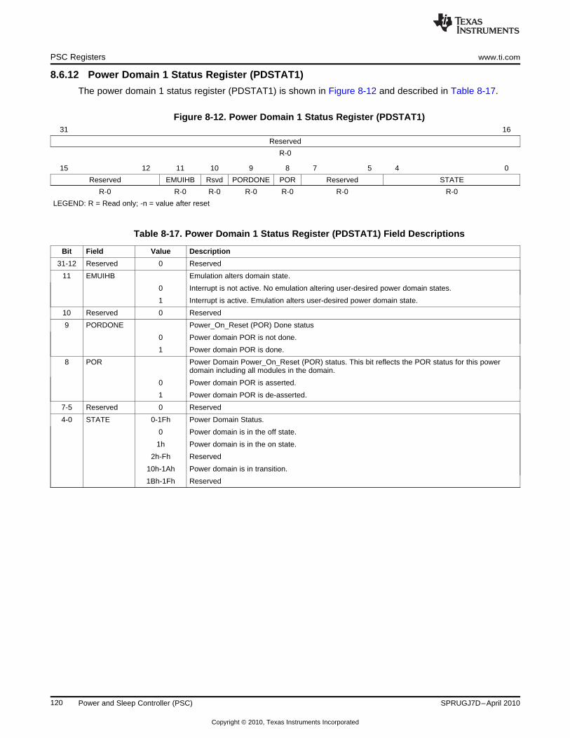
PSC Registers www.ti.com
8.6.12 Power Domain 1 Status Register (PDSTAT1)
The power domain 1 status register (PDSTAT1) is shown in Figure 8-12 and described in Table 8-17.
Figure 8-12. Power Domain 1 Status Register (PDSTAT1)31 16
Reserved
R-0
15 12 11 10 9 8 7 5 4 0
Reserved EMUIHB Rsvd PORDONE POR Reserved STATE
R-0 R-0 R-0 R-0 R-0 R-0 R-0
LEGEND: R = Read only; -n = value after reset
Table 8-17. Power Domain 1 Status Register (PDSTAT1) Field Descriptions
Bit Field Value Description
31-12 Reserved 0 Reserved
11 EMUIHB Emulation alters domain state.
0 Interrupt is not active. No emulation altering user-desired power domain states.
1 Interrupt is active. Emulation alters user-desired power domain state.
10 Reserved 0 Reserved
9 PORDONE Power_On_Reset (POR) Done status
0 Power domain POR is not done.
1 Power domain POR is done.
8 POR Power Domain Power_On_Reset (POR) status. This bit reflects the POR status for this powerdomain including all modules in the domain.
0 Power domain POR is asserted.
1 Power domain POR is de-asserted.
7-5 Reserved 0 Reserved
4-0 STATE 0-1Fh Power Domain Status.
0 Power domain is in the off state.
1h Power domain is in the on state.
2h-Fh Reserved
10h-1Ah Power domain is in transition.
1Bh-1Fh Reserved
120 Power and Sleep Controller (PSC) SPRUGJ7D–April 2010
Copyright © 2010, Texas Instruments Incorporated

www.ti.com PSC Registers
8.6.13 Power Domain 0 Control Register (PDCTL0)
The power domain 0 control register (PDCTL0) is shown in Figure 8-13 and described in Table 8-18.
Figure 8-13. Power Domain 0 Control Register (PDCTL0)31 24 23 16
Reserved WAKECNT
R-0 R/W-1Fh
15 12 11 10 9 8 7 1 0
PDMODE Reserved EMUIHBIE Rsvd Reserved NEXT
R-Fh R-0 R/W-0 R-1 R-0 R/W-1
LEGEND: R/W = Read/Write; R = Read only; -n = value after reset
Table 8-18. Power Domain 0 Control Register (PDCTL0) Field Descriptions
Bit Field Value Description
31-24 Reserved 0 Reserved
23-16 WAKECNT 0-FFh RAM wake count delay value. Not recommended to change the default value (1Fh). Bits 23-30:GOOD2ACCESS wake delay. Bits 19-16: ON2GOOD wake delay.
15-12 PDMODE 0-Fh Power down mode.
0-Eh Reserved
Fh Core on, RAM array on, RAM periphery on.
11-10 Reserved 0 Reserved
9 EMUIHBIE Emulation alters power domain state interrupt enable.
0 Disable interrupt.
1 Enable interrupt.
8 Reserved 1 Reserved
7-1 Reserved 0 Reserved
0 NEXT Power domain next state. For Always ON power domain this bit is read/write, but writes have no effectsince internally this power domain always remains in the on state.
0 Power domain off.
1 Power domain on.
121SPRUGJ7D–April 2010 Power and Sleep Controller (PSC)
Copyright © 2010, Texas Instruments Incorporated

PSC Registers www.ti.com
8.6.14 Power Domain 1 Control Register (PDCTL1)
The power domain 1 control register (PDCTL1) is shown in Figure 8-14 and described in Table 8-19.
Figure 8-14. Power Domain 1 Control Register (PDCTL1)31 24 23 16
Reserved WAKECNT
R-0 R/W-1Fh
15 12 11 10 9 8 7 1 0
PDMODE Reserved EMUIHBIE Rsvd Reserved NEXT
R-Fh R-0 R/W-0 R-1 R-0 R/W-1
LEGEND: R/W = Read/Write; R = Read only; -n = value after reset
Table 8-19. Power Domain 1 Control Register (PDCTL1) Field Descriptions
Bit Field Value Description
31-24 Reserved 0 Reserved
23-16 WAKECNT 0-FFh RAM wake count delay value. Not recommended to change the default value (1Fh). Bits 23-30:GOOD2ACCESS wake delay. Bits 19-16: ON2GOOD wake delay.
15-12 PDMODE 0-Fh Power down mode.
0 Core off, RAM array off, RAM periphery off.
1h Core off, RAM array retention, RAM periphery off (deep sleep).
2h-3h Reserved
4h Core retention, RAM array off, RAM periphery off.
5h Core retention, RAM array retention, RAM periphery off (deep sleep).
6h-7h Reserved
8h Core on, RAM array off, RAM periphery off.
9h Core on, RAM array retention, RAM periphery off (deep sleep).
Ah Core on, RAM array retention, RAM periphery off (light sleep).
Bh Core on, RAM array retention, RAM periphery on.
Ch-Eh Reserved
Fh Core on, RAM array on, RAM periphery on.
11-10 Reserved 0 Reserved
9 EMUIHBIE Emulation alters power domain state interrupt enable.
0 Disable interrupt.
1 Enable interrupt.
8 Reserved 1 Reserved
7-1 Reserved 0 Reserved
0 NEXT User-desired power domain next state.
0 Power domain off.
1 Power domain on.
122 Power and Sleep Controller (PSC) SPRUGJ7D–April 2010
Copyright © 2010, Texas Instruments Incorporated

www.ti.com PSC Registers
8.6.15 Power Domain 0 Configuration Register (PDCFG0)
The power domain 0 configuration register (PDCFG0) is shown in Figure 8-15 and described inTable 8-20.
Figure 8-15. Power Domain 0 Configuration Register (PDCFG0)31 16
Reserved
R-0
15 4 3 2 1 0
Reserved PD_LOCK ICEPICK RAM_PSM ALWAYSON
R-0 R-1 R-1 R-0 R-1
LEGEND: R = Read only; -n = value after reset
Table 8-20. Power Domain 0 Configuration Register (PDCFG0) Field Descriptions
Bit Field Value Description
31-4 Reserved 0 Reserved
3 PD_LOCK PDCTL.NEXT lock. For Always ON power domain this bit is a don't care.
0 PDCTL.NEXT bit is locked and cannot be changed in software.
1 PDCTL.NEXT bit is not locked.
2 ICEPICK IcePick support.
0 Not present
1 Present
1 RAM_PSM RAM power domain.
0 Not a RAM power domain.
1 RAM power domain.
0 ALWAYSON Always ON power domain.
0 Not an Always ON power domain.
1 Always ON power domain.
123SPRUGJ7D–April 2010 Power and Sleep Controller (PSC)
Copyright © 2010, Texas Instruments Incorporated
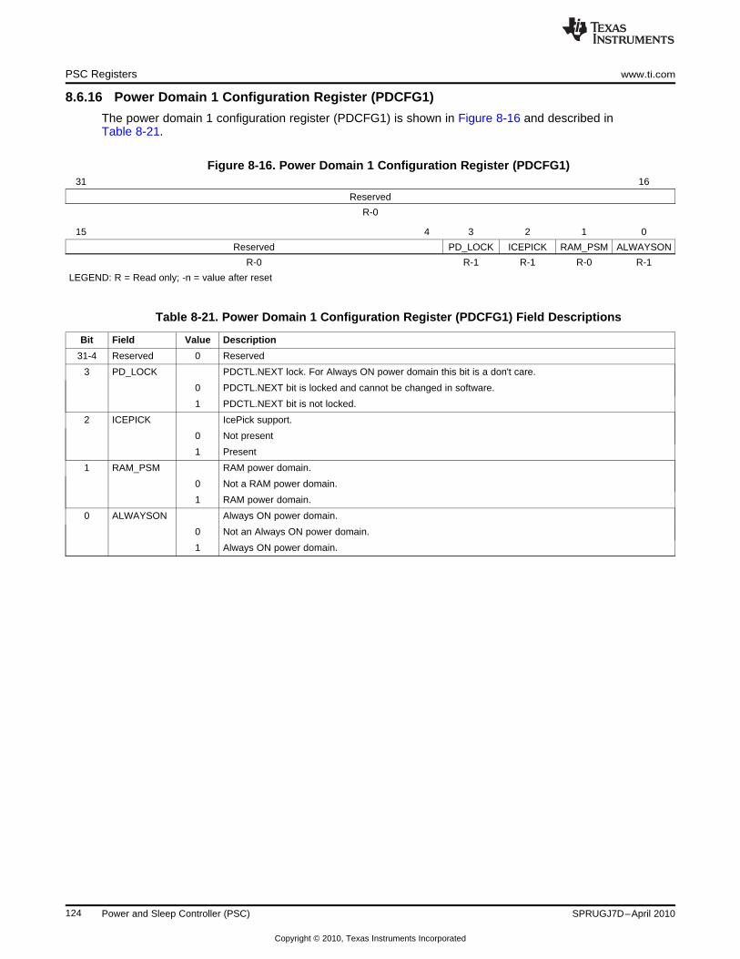
PSC Registers www.ti.com
8.6.16 Power Domain 1 Configuration Register (PDCFG1)
The power domain 1 configuration register (PDCFG1) is shown in Figure 8-16 and described inTable 8-21.
Figure 8-16. Power Domain 1 Configuration Register (PDCFG1)31 16
Reserved
R-0
15 4 3 2 1 0
Reserved PD_LOCK ICEPICK RAM_PSM ALWAYSON
R-0 R-1 R-1 R-0 R-1
LEGEND: R = Read only; -n = value after reset
Table 8-21. Power Domain 1 Configuration Register (PDCFG1) Field Descriptions
Bit Field Value Description
31-4 Reserved 0 Reserved
3 PD_LOCK PDCTL.NEXT lock. For Always ON power domain this bit is a don't care.
0 PDCTL.NEXT bit is locked and cannot be changed in software.
1 PDCTL.NEXT bit is not locked.
2 ICEPICK IcePick support.
0 Not present
1 Present
1 RAM_PSM RAM power domain.
0 Not a RAM power domain.
1 RAM power domain.
0 ALWAYSON Always ON power domain.
0 Not an Always ON power domain.
1 Always ON power domain.
124 Power and Sleep Controller (PSC) SPRUGJ7D–April 2010
Copyright © 2010, Texas Instruments Incorporated

www.ti.com PSC Registers
8.6.17 Module Status n Register (MDSTATn)
The module status n register (MDSTATn) is shown in Figure 8-17 and described in Table 8-22.
Figure 8-17. Module Status n Register (MDSTATn)31 18 17 16
Reserved EMUIHB EMURST
R-0 R-0 R-0
15 13 12 11 10 9 8 7 6 5 0
Reserved MCKOUT Rsvd MRST LRSTDONE LRST Reserved STATE
R-0 R-0 R-1 R-0 R-1 R-1 R-0 R-0
LEGEND: R = Read only; -n = value after reset
Table 8-22. Module Status n Register (MDSTATn) Field Descriptions
Bit Field Value Description
31-18 Reserved 0 Reserved
17 EMUIHB Emulation alters module state. This bit applies to DSP module (module 15). This field is 0 for allother modules.
0 No emulation altering user-desired module state programmed in the NEXT bit in the module control15 register (MDCTL15).
1 Emulation altered user-desired state programmed in the NEXT bit in MDCTL15. If you desire togenerate a PSCINT upon this event, you must set the EMUIHBIE bit in MDCTL15.
16 EMURST Emulation alters module reset. This bit applies to DSP module (module 15). This field is 0 for allother modules.
0 No emulation altering user-desired module reset state.
1 Emulation altered user-desired module reset state. If you desire to generate a PSCINT upon thisevent, you must set the EMURSTIE bit in the module control 15 register (MDCTL15).
15-13 Reserved 0 Reserved
12 MCKOUT Module clock output status. Shows status of module clock.
0 Module clock is off.
1 Module clock is on.
11 Reserved 1 Reserved
10 MRST Module reset status. Reflects actual state of module reset.
0 Module reset is asserted.
1 Module reset is de-asserted.
9 LRSTDONE Local reset done. Software is responsible for checking if local reset is done before accessing thismodule. This bit applies to DSP module (module 15). This field is 1 for all other modules.
0 Local reset is not done.
1 Local reset is done.
8 LRST Module local reset status. This bit applies to DSP module (module 15).
0 Local reset is asserted.
1 Local reset is de-asserted.
7-6 Reserved 0 Reserved
5-0 STATE 0-3Fh Module state status: indicates current module status.
0 SwRstDisable state
1h SyncReset state
2h Disable state
3h Enable state
4h-3Fh Indicates transition
125SPRUGJ7D–April 2010 Power and Sleep Controller (PSC)
Copyright © 2010, Texas Instruments Incorporated
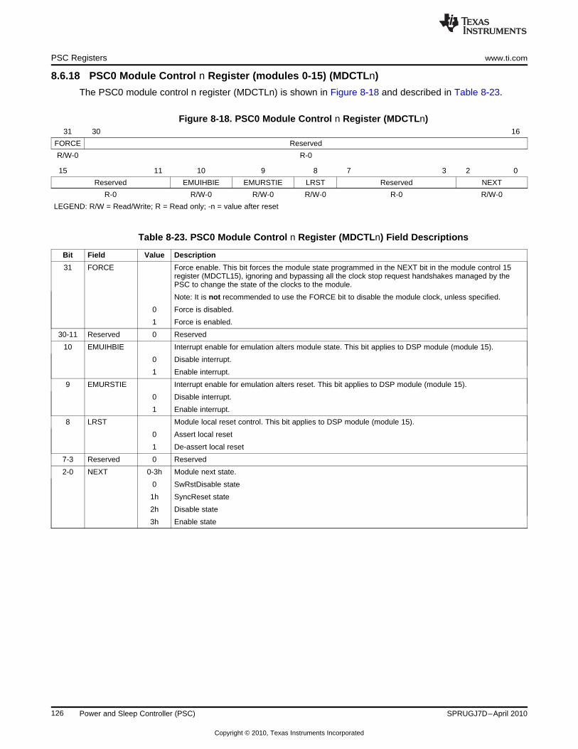
PSC Registers www.ti.com
8.6.18 PSC0 Module Control n Register (modules 0-15) (MDCTLn)
The PSC0 module control n register (MDCTLn) is shown in Figure 8-18 and described in Table 8-23.
Figure 8-18. PSC0 Module Control n Register (MDCTLn)31 30 16
FORCE Reserved
R/W-0 R-0
15 11 10 9 8 7 3 2 0
Reserved EMUIHBIE EMURSTIE LRST Reserved NEXT
R-0 R/W-0 R/W-0 R/W-0 R-0 R/W-0
LEGEND: R/W = Read/Write; R = Read only; -n = value after reset
Table 8-23. PSC0 Module Control n Register (MDCTLn) Field Descriptions
Bit Field Value Description
31 FORCE Force enable. This bit forces the module state programmed in the NEXT bit in the module control 15register (MDCTL15), ignoring and bypassing all the clock stop request handshakes managed by thePSC to change the state of the clocks to the module.
Note: It is not recommended to use the FORCE bit to disable the module clock, unless specified.
0 Force is disabled.
1 Force is enabled.
30-11 Reserved 0 Reserved
10 EMUIHBIE Interrupt enable for emulation alters module state. This bit applies to DSP module (module 15).
0 Disable interrupt.
1 Enable interrupt.
9 EMURSTIE Interrupt enable for emulation alters reset. This bit applies to DSP module (module 15).
0 Disable interrupt.
1 Enable interrupt.
8 LRST Module local reset control. This bit applies to DSP module (module 15).
0 Assert local reset
1 De-assert local reset
7-3 Reserved 0 Reserved
2-0 NEXT 0-3h Module next state.
0 SwRstDisable state
1h SyncReset state
2h Disable state
3h Enable state
126 Power and Sleep Controller (PSC) SPRUGJ7D–April 2010
Copyright © 2010, Texas Instruments Incorporated

www.ti.com PSC Registers
8.6.19 PSC1 Module Control n Register (modules 0-31) (MDCTLn)
The PSC1 module control n register (MDCTLn) is shown in Figure 8-19 and described in Table 8-24.
Figure 8-19. PSC1 Module Control n Register (MDCTLn)31 30 16
FORCE Reserved
R/W-0 R-0
15 3 2 0
Reserved NEXT
R-0 R/W-0
LEGEND: R/W = Read/Write; R = Read only; -n = value after reset
Table 8-24. PSC1 Module Control n Register (MDCTLn) Field Descriptions
Bit Field Value Description
31 FORCE Force enable. This bit forces the module state programmed in the NEXT bit in the module control 15register (MDCTL15), ignoring and bypassing all the clock stop request handshakes managed by thePSC to change the state of the clocks to the module.
Note: It is not recommended to use the FORCE bit to disable the module clock, unless specified.
0 Force is disabled.
1 Force is enabled.
30-3 Reserved 0 Reserved
2-0 NEXT 0-3h Module next state.
0 SwRstDisable state
1h SyncReset state
2h Disable state
3h Enable state
127SPRUGJ7D–April 2010 Power and Sleep Controller (PSC)
Copyright © 2010, Texas Instruments Incorporated

128 Power and Sleep Controller (PSC) SPRUGJ7D–April 2010
Copyright © 2010, Texas Instruments Incorporated
Chapter 9SPRUGJ7D–April 2010
Power Management
Topic ........................................................................................................................... Page
9.1 Introduction .................................................................................................... 1309.2 Power Consumption Overview .......................................................................... 1309.3 PSC and PLLC Overview .................................................................................. 1309.4 Features ......................................................................................................... 1319.5 Clock Management .......................................................................................... 1329.6 DSP Sleep Mode Management ........................................................................... 1339.7 RTC-Only Mode ............................................................................................... 1339.8 Dynamic Voltage and Frequency Scaling (DVFS) ................................................. 1339.9 Deep Sleep Mode ............................................................................................. 1359.10 Additional Peripheral Power Management Considerations .................................... 138
129SPRUGJ7D–April 2010 Power Management
Copyright © 2010, Texas Instruments Incorporated

Introduction www.ti.com
9.1 Introduction
Power management is an important aspect for most embedded applications. For several applications andtarget markets, there may be a specific power budget and requirements to minimize power consumptionfor both power supply sizing and battery life considerations. Additionally, lower power consumption resultsin more optimal and efficient designs from cost, design, and energy perspectives. This device has severalmeans of managing the power consumption. This chapter discusses the various power managementfeatures.
9.2 Power Consumption Overview
Power consumed by semiconductor devices has two components: dynamic and static. This can be shownas:
Ptotal = Pdynamic + Pstatic
The dynamic power is the power consumed to perform work when the device is in active modes (clocksapplied, busses, and I/O switching), that is, analog circuits changing states. The dynamic power is definedby:
Pdynamic = Capacitance × Voltage2 × Frequency
From the above formula, the dynamic power scales with the clock frequency (device/module frequency forcore operations and switching frequency for I/O). Dynamic power can be reduced by controlling the clocksin such a way as to either operate at a clock setting just high enough to complete the required operation inthe required timeline or to run at a clock setting until the work is complete and then drastically reduce theclock frequency or cut off the clocks until additional work must be performed.
In the formula, the dynamic power varies with the voltage squared, so the voltage of operations hassignificant impact on overall power consumption and, thus, on the battery life. Dynamic power can bereduced by scaling the operating voltage, when the performance requirements are not that high and thedevice can be operated at a corresponding lower frequency.
The capacitance is the capacitance of the switching nodes, or the load capacitances on the switching I/Opins.
The static power, as the name suggests, is independent of the switching frequency of the logic. It can beshown as:
Pstatic = f(leakage current)
It is essentially a function of the “leakage”, or the power consumed by the logic when it is not switching oris not performing any work. Leakage current is dependent mostly on the manufacturing process used, thesize of the die, etc. Leakage current is unavoidable while power is applied and scales roughly with theoperating junction temperatures. Leakage power can only be avoided by removing power completely froma device or subsystem. The static power consumption plays a significant role in the Standby Modes (whenthe application is not running and in a dormant state) and plays an important role in the battery life forportable applications, etc.
9.3 PSC and PLLC Overview
The power and sleep controller (PSC) module plays an important role in managing the enabling/disablingof the clocks to the core and various peripheral modules. The PSC provides a granular support to turnon/off clocks on a module by module basis. Similarly, the two PLL controllers (PLLC0 and PLLC1) play animportant role in device and module clock generation, and manage the frequency scaling operations forthe device. Together these modules play a significant role in managing the clocks from a powermanagement feature standpoint. For detailed information on the PSC, see Chapter 8. For detailedinformation on the PLLC0 and PLLC1, see Chapter 6 and Chapter 7.
130 Power Management SPRUGJ7D–April 2010
Copyright © 2010, Texas Instruments Incorporated

www.ti.com Features
9.4 Features
This device has several means of managing power consumption, as detailed in the subsequent sections.This device uses the state-of-the-art 65 nm process, which provides a good balance on power andperformance, providing high-performance transistors with relatively less leakage current and, thereby, lowstandby-power consumption modes.
There are several features in design as well as user driven software control to reduce dynamic powerconsumption. The design features (not under user control) include a power optimized clock tree design toreduce overall clock tree power consumption and automatic clock gating in several modules when thelogic in the modules is not active.
The on-chip power and sleep controller (PSC) module provides granular software controlled module levelclock gating, which reduces both clock tree and module power by basically disabling the clocks when themodules are not being used. Clock management also allows you to slow down the clocks, to reduce thedynamic power.
Table 9-1 describes the power management features.
Table 9-1. Power Management Features
Power Management Description Features
Clock Management
PLL bypass and Both PLLs can be powered-down and run in Reduces the dynamic power consumption of thepower-down bypass mode when not in use. core.
Module clock ON Module clocks can be turned on/off without Reduces the dynamic power consumption of therequiring reconfiguring the registers. core and I/O (if any free running I/O clocks).
Core Sleep Management
DSP subsystem The DSP CPU can be put in sleep (IDLE) mode. Reduces the dynamic power consumption.sleep mode
Voltage Management
RTC-only mode Allows removing power from all core and I/O Reduces the dynamic and static power for standbysupply and just have the real-time clock (RTC) modes that require only the RTC to be functional.running.
Dynamic Voltage and Frequency Scaling
Dynamic Voltage and The operating voltage and frequency of the device Reduces the dynamic power consumption of theFrequency Scaling can be dynamically scaled to meet the core and I/O as well as standby power(DVFS) requirements of the application.
System/Device Sleep Management
Deep Sleep Mode All internal clocks of the device can be turned Reduces the dynamic power consumption of theon/off at the MXI/CLKIN level. The deep sleep core and I/O.function can be controlled externally through theDEESLEEP pin or internally through theRTC_ALARM pin.
Peripheral I/O Power Management
USB PHY power-down The USB2.0 PHY can be powered-down. Minimizes the USB2.0 I/O power consumptionwhen not in use.
DDR2/mDDR Allows memory to retain its contents while the rest mDDR and DDR2 can be clock gated to reduce theself-refresh mode of the system is powered down. dynamic power consumption or the entire device
can be powered down to reduce the static powerconsumption.
SATA PHY power-down The SATA PHY can be placed in standby mode. Minimizes the SATA I/O power consumption whennot in use.
LVCMOS I/O buffer LVCMOS I/O buffer receivers are disabled. Minimizes the I/O power consumption.receiver disable
Internal pull-up and The internal pull-ups and pull-downs are Reduces the I/O leakage power.pull-down resistor enabled/disabled by groups.control
131SPRUGJ7D–April 2010 Power Management
Copyright © 2010, Texas Instruments Incorporated

Clock Management www.ti.com
9.5 Clock Management
9.5.1 Module Clock ON/OFF
The module clock on/off feature allows software to disable clocks to module individually, in order to reducethe module's dynamic/switching power consumption down to zero. This device is designed in full staticCMOS; thus, when a module clock stops, the module's state is preserved and retained. When the clock isrestarted, the module resumes operating from the stopping point.
NOTE: Stopping clocks to a module only affects dynamic power consumption, it does not affectstatic power consumption of the module or the device.
The power and sleep controller (PSC) module controls module clock gating. If a module's clock(s) isstopped while being accessed, the access may not occur, and it can potentially result in unexpectedbehavior. The PSC provides some protection against such erroneous conditions by monitoring the internalbus activity to ensure there are no accesses to the module from the internal bus, before allowing module’sinternal clock to be gated. However, it is still recommended that software must ensure that all of thetransactions to the module are finished prior to disabling the clocks.
The procedure to turn module clocks on/off using the PSC is described in Chapter 8.
NOTE: To preserve the state of the module, the module state in the PSC must be set to Disable. Inthis state, the module reset is not asserted and only the module clock is turned off.
Furthermore, special consideration must be given to DSP clock on/off. The procedure to turn the coreclock on/off is further described in .
Additionally some peripherals implement additional power saving features by automatically shutting ofclock to components within the module, when the logic is not active. This is transparent to you, butreduces overall dynamic power consumption when modules are not active.
9.5.2 Module Clock Frequency Scaling
Module clock frequency is scalable by programming the PLL multiply and divide parameters. Additionally,some modules might also have internal clock dividers. Reducing the clock frequency reduces thedynamic/switching power consumption, which scales linearly with frequency.
Chapter 6 details the clocking structure of the device. Chapter 7 describes how to program the PLL0 andPLL1 frequency and the frequency constraints.
9.5.3 PLL Bypass and Power Down
You can bypass each PLL in this device. Bypassing the PLL sends a bypass clock instead of the PLLVCO output (PLLOUT) to the system clocks of the PLLC. For PLLC0, the bypass clock is selected fromeither the PLL reference clock (MXI/CLKIN) or PLL1_SYSCLK3. For PLLC1, the bypass clock is alwaysMXI/CLKIN. The MXI/CLKIN frequency is typically, at most, up to 50 MHZ.
You can use the MXI/CLKIN bypass mode to reduce the core and module clock frequencies to very lowmaintenance levels without using the PLL during periods of very low system activity. This can lower theoverall dynamic power consumption, which is linearly proportional to the frequency.
When the PLL controller is placed in bypass mode, the PLL retains its frequency lock. This allows you toswitch between bypass mode and PLL mode without having to wait for the PLL to relock. However,keeping the PLL locked consumes power. You can also power-down the PLL when bypassing it tominimize the overall power consumed by the PLL module. The advantage of bypassing the PLL withoutpowering it down is that you do not have to incur the PLL lock time when switching back to a normaloperating level.
Chapter 6 and Chapter 7 describe PLL bypass and PLL power down.
132 Power Management SPRUGJ7D–April 2010
Copyright © 2010, Texas Instruments Incorporated

www.ti.com DSP Sleep Mode Management
9.6 DSP Sleep Mode Management
9.6.1 C674x DSP CPU Sleep Mode
The DSP CPU can be put in a low-power state by executing the IDLE instruction. For information on theIDLE instruction, see the TMS320C674x DSP CPU and Instruction Set Reference Guide (SPRUFE8).
9.6.2 C674x Megamodule Sleep Mode
The IDLE instruction is used as part of the procedure for shutting down the entire C674x megamodule, bythe power-down controller (PDC) module. In shutting down the entire C674x megamodule, the PDC caninternally clock gate off the following components of the megamodule and internal memories of the DSPsubsystem:
• C674x CPU• Program Memory Controller (PMC)• Data Memory Controller (DMC)• Unified Memory Controller (UMC)• Extended Memory Controller (EMC)• L1P Memory• L1D Memory• L2 Memory
Putting the entire C674x megamodule into the low-power sleep mode is typically more useful and saves alot more power, as compared to just executing the IDLE instruction to put only the CPU in idle mode.
For information on putting the C674x megamodule in the low-power mode using the PDC, see theTMS320C674x DSP Megamodule Reference Guide (SPRUFK5).
9.7 RTC-Only Mode
In real-time clock (RTC)-only mode, the RTC is powered on and the rest of the device is completelypowered off (all supplies except the RTC supply are removed). In this mode, the RTC is fully functionaland keeps track of date, hours, minutes, and seconds. In this mode, the overall power consumption wouldbe significantly lower, as voltage from the rest of the core and I/O logic can be completely removed,eliminating most of the active and static power of the device, except for what is consumed by the RTCmodule, running at 32 kHz.
NOTE: To put the device in RTC-only mode, there is no software control sequence. You can putthe device in the RTC-only mode by removing the power supply from all core and I/O logic,except for the RTC core logic supply (RTC_CVDD). During wake up, all power sequencingrequirements described in the device-specific data manual must be followed.
Some limitations apply in the RTC-only mode. First, the RTC_ALARM pin is not available as an option foruse as a control to signal an external power supply to reapply power to the rest of the device. This isbecause the RTC_ALARM pin is powered by the I/O supply that is powered down in RTC-only mode.Second, in RTC-only mode, only the RTC register contents are preserved, all other internal memory andregister contents are lost. Mobile DDR and DDR2 contents can be preserved through the use ofself-refresh (see Section 9.9.2). However, software must be in place to restore the context of the device,for example, reinitialize internal registers, setup cache memory configurations, interrupt vectors, etc.
9.8 Dynamic Voltage and Frequency Scaling (DVFS)
Dynamic voltage and frequency scaling (DVFS) consists of minimizing the idle time of the system. TheDVFS technique uses dynamic selection of the optimal frequency and voltage to allow a task to beperformed in the required amount of time. This reduces the total power consumption of the device whilestill meeting task requirements. DVFS requires control over the clock frequency and the operating voltageof the device elements. By intelligently switching these elements to their optimal operating points, it ispossible to minimize the power consumption of the device for a given task.
133SPRUGJ7D–April 2010 Power Management
Copyright © 2010, Texas Instruments Incorporated

Dynamic Voltage and Frequency Scaling (DVFS) www.ti.com
For reasons related to the device (clock architecture, process, etc.), DVFS is used only for a few discretesteps, not over a continuum of voltage and frequency values. Each step, or operating performance point(OPP), is composed of a voltage and frequency pair. For an OPP, the frequency corresponds to themaximum frequency allowed at a voltage, or reciprocally; the voltage corresponds to the minimum voltageallowed for a frequency. See your device data manual for a list of the OPPs supported by the device.
When applying DVFS, a processor or system always runs at the lowest OPP that meets the performancerequirement at a given time. You determine the optimal OPP for a given task and then switch to that OPPto save power.
9.8.1 Frequency Scaling Considerations
The operating frequency of the device is controlled through its two PLL controllers (PLLC0 and PLLC1).Through a series of multipliers and dividers you can change the frequencies of various clocks throughoutthe device. See Chapter 6 for information on the clock architecture of the device and see Chapter 7 forinformation on the PLL controllers. A few things must be noted when changing the various internalfrequencies of the device:
• Changing the SYSCLK frequencyThe PLL_VCO (PLLOUT) frequency can be programmed through a PLL multiplier. A series of dividersdivide PLLOUT to generate the various device SYSCLKs.To change the SYSCLK frequency you can change the PLL multiplier or you can change the SYSCLKdivider ratio. When changing the PLL multiplier, you must put the PLL controller in bypass mode whilethe PLL multiplier value is modified and a lock on the new frequency is reached. The lock time is givenin the device data manual. When changing the divider ratios it is not required to put the PLL controllerin bypass mode.Changing the SYSCLK frequency through the dividers is faster as there is no need to reprogram thePLL. However, the SYSCLK frequency will depend solely on the divider ratios used.
• SYSCLK domain fixed ratiosCertain SYSCLK domains need to operate at a fixed ratio with respect to the CPU clock. Care shouldbe taken to ensure that these fixed ratios are maintained. For additional details, see Chapter 6.
• PLLC0 bypass clockWhen switching the PLL multiplier, the PLL controller must be placed in bypass mode. Bypassing thePLL sends a bypass clock instead of the PLL VCO output (PLLOUT) to the system clock dividers ofthe PLL controller.For PLLC0 the bypass clock is selected from either the PLL reference clock (MXI/CLKIN) orPLL1_SYSCLK3. For PLLC1, the bypass clock is always MXI/CLKIN. The MXI/CLKIN frequency istypically, at most, up to 50 MHZ.You can use the MXI/CLKIN bypass mode to reduce the core and module clock frequencies to verylow maintenance levels without using the PLL during periods of very low system activity.It may be desirable for the bypass clock to not revert to MXI/CLKIN in some situations to preservedbandwidth during frequency scaling transitions. For this reason, the PLLC0 bypass clock can be set toPLL1_SYSCLK3. This selection is made through the EXTCLKSRC bit in the PLLCTL register ofPLLC0.
• Peripheral immunity from CPU clock frequency changesPeripherals that are clocked by the PLL0_AUXCLK are immune to changes in the PLL0 frequency.The PLL0_AUXCLK is derived from MXI/CLKIN.Peripherals in the ASYNC3 domain are clocked off from either PLL1_SYSCLK2 or PLL0_SYSCLK2.Furthermore, PLL0_SYSCLK2 must always be /2 of the CPU clock frequency. To keep theseperipherals immune from changes in PLL0 frequency (such as when the CPU frequency is modified),you can configure the ASYNC3 domain to be clocked from PLL1_SYSCLK2. PLL1 is mainly used toclock the DDR2/mDDR memory controller.When peripherals are immune to changes in the CPU clock frequency, their internal clock dividers donot have to be adjusted for changes in their input clock frequencies.
134 Power Management SPRUGJ7D–April 2010
Copyright © 2010, Texas Instruments Incorporated
www.ti.com Deep Sleep Mode
9.8.2 Voltage Scaling Considerations
The operating voltage of the device must be totally controlled through mechanisms outside the device. I2Cports on the device can be used to communicate with external power management chips. A few thingsmust be noted when changing the operating voltage of the device:
• Voltage ramp rate: The ramp rate of the operating voltage must be observed during operatingperformance point (OPP) transitions. See the device data manual for ramp rate specifications.
• Switching to a lower voltage: When switching to a lower voltage, the maximum operating frequencychanges. Care must be taken such that the maximum operating frequency supported at the newvoltage is not violated. For this reason, it is recommended to change the operating frequency beforeswitching the operating voltage.
9.9 Deep Sleep Mode
This device supports a Deep Sleep mode where all device clocks are stopped and the on-chip oscillator isshut down to save power. Registers and memory contents are preserved, thus, upon recovery, theprogram may continue from where it left off with minimal overhead involved.
The Deep Sleep mode is initiated when the DEEPSLEEP pin is driven low. The device wakes up fromDeep Sleep mode when the DEEPSLEEP pin is driven high. The DEEPSLEEP pin can be driven by anexternal controller or it can be driven internally by the real-time clock (RTC). The RTC method allows forautomatic wake-up at a programmed time.
9.9.1 Entering/Exiting Deep Sleep Mode Using Externally Controlled Wake-Up
9.9.1.1 Entering Deep Sleep Mode
Use the following procedure to enter the Deep Sleep mode if an external signal is used:
1. The DDR2/mDDR should be clock gated (see Section 9.10.2). To preserve DDR2/mDDR memorycontents, activate the self-refresh mode. You can use partial array self-refresh (PASR) for additionalpower savings for mDDR memory.
2. The SATA PHY should be disabled (see Section 9.10.3).3. The USB2.0 (USB0) PHY should be disabled, if this interface is used and internal clocks are selected
(see Section 9.10.1).4. The USB1.1 (USB1) PHY should be disabled, if this interface is used and internal clocks are selected
(see Section 9.10.1).5. PLL/PLLC0 and PLL/PLLC1 should be placed in bypass mode (clear the PLLEN bit in the PLL control
register (PLLCTL) of each PLLC to 0).6. PLL/PLLC0 and PLL/PLLC1 should be powered down (set the PLLPWRDN bit in PLLCTL of each
PLLC to 1).7. Configure the DEEPSLEEP pin as input-only using the PINMUX0_31_28 bits in the PINMUX0 register.8. The external controller should drive the DEEPSLEEP pin high (not in Deep Sleep).9. Configure the desired delay in the SLEEPCOUNT bit field in the deep sleep register (DEEPSLEEP) in
the System Configuration Module. This count determines the delay before the Deep Sleep logicreleases the clocks to the device during wake up (allowing the oscillator to stabilize).
10. Set the SLEEPENABLE bit in DEEPSLEEP to 1. This automatically clears the SLEEPCOMPLETE bit.11. Begin polling the SLEEPCOMPLETE bit until it is set to 1. This bit is set once the device is woken up
from Deep Sleep mode.12. The external controller drives the DEEPSLEEP pin low to initiate Deep Sleep mode.
135SPRUGJ7D–April 2010 Power Management
Copyright © 2010, Texas Instruments Incorporated

Deep Sleep Mode www.ti.com
9.9.1.2 Exiting Deep Sleep Mode
Use the following procedure to exit the Deep Sleep state if an external signal is used:
1. The external controller drives the DEEPSLEEP pin high.2. When the SLEEPCOUNT delay is complete, the Deep Sleep logic releases the clock to the device and
sets the SLEEPCOMPLETE bit in the deep sleep register (DEEPSLEEP) in the System ConfigurationModule.
3. Clear the SLEEPENABLE bit in DEEPSLEEP to 0. This automatically clears the SLEEPCOMPLETEbit.
4. Initialize the PLL controllers as described in Section 7.2.2.2. Note that the state of the PLL controllerregisters is preserved during Deep Sleep mode. Therefore, it is not necessary to reprogram all the PLLcontroller registers unless a new setting is desired. At minimum, steps 3, 4, and 7-10 of the PLLinitialization procedure must be followed.
5. Configure the desired states to the peripherals and enable as required.
9.9.2 Entering/Exiting Deep Sleep Mode Using RTC Controlled Wake-Up
9.9.2.1 Entering Deep Sleep Mode
Use the following procedure to enter the Deep Sleep state if the RTC is used to wake-up the device:
1. The DDR2/mDDR should be clock gated (see Section 9.10.2). To preserve DDR2/mDDR memorycontents, activate the self-refresh mode. You can use partial array self-refresh (PASR) for additionalpower savings for mDDR memory.
2. The SATA PHY should be disabled (see Section 9.10.3).3. The USB2.0 (USB0) PHY should be disabled, if this interface is used and internal clocks are selected
(see Section 9.10.1).4. The USB1.1 (USB1) PHY should be disabled, if this interface is used and internal clocks are selected
(see Section 9.10.1).5. PLL/PLLC0 and PLL/PLLC1 should be placed in bypass mode (clear the PLLEN bit in the PLL control
register (PLLCTL) of each PLLC to 0).6. PLL/PLLC0 and PLL/PLLC1 should be powered down (set the PLLPWRDN bit in PLLCTL of each
PLLC to 1).7. Configure the desired wake-up time as an alarm in the RTC.8. Configure the DEEPSLEEP/RTC_ALARM pin to output RTC_ALARM using the PINMUX0_31_28 bits
in the PINMUX0 register. The pin is driven low since the alarm has not yet occurred.9. Configure the desired delay in the SLEEPCOUNT bit field in the deep sleep register (DEEPSLEEP) in
the System Configuration Module. This count determines the delay before the Deep Sleep logicreleases the clocks to the device during wake up (allowing the oscillator to stabilize).
10. Set the SLEEPENABLE bit in DEEPSLEEP to 1. This automatically clears the SLEEPCOMPLETE bit.Also, the device now enters the Deep Sleep mode since the DEEPSLEEP pin is low.
9.9.2.2 Exiting Deep Sleep Mode
Use the following procedure to exit the Deep Sleep state if the RTC is used to wake-up the device:
1. The RTC alarm occurs and the RTC_ALARM pin is driven high (which is internally connected to theDEEPSLEEP pin). This causes the Deep Sleep logic to exit the Deep Sleep mode.
2. When the SLEEPCOUNT delay is complete, the Deep Sleep logic releases the clock to the device andsets the SLEEPCOMPLETE bit in the deep sleep register (DEEPSLEEP) in the System ConfigurationModule.
3. Clear the SLEEPENABLE bit in DEEPSLEEP to 0. This automatically clears the SLEEPCOMPLETEbit.
4. Configure the desired state to the PLL controllers.5. Remove the PLLs from power down (clear the PLLPWRDN bit in the PLL control register (PLLCTL) of
each PLLC to 0).6. Set the PLL controllers to PLL mode (set the PLLEN bit in PLLCTL of each PLLC to 1).
136 Power Management SPRUGJ7D–April 2010
Copyright © 2010, Texas Instruments Incorporated

SLEEPENABLE(internal)
DEEPSLEEP
CLKGATE(internal)
OSC_GZ(internal)
PLLC Ref Clk(internal)
MXI/CLKIN
SLEEPCOMPLETE(internal)
See Note: 1 2 3 4 5 6 7 8
www.ti.com Deep Sleep Mode
7. Configure the desired states to the peripherals and enable as required.
9.9.3 Deep Sleep Sequence
Figure 9-1 illustrates the Deep Sleep sequence:
1. Software sets the SLEEPENABLE bit in the deep sleep register (DEEPSLEEP) in the SystemConfiguration Module.
2. The DEEPSLEEP pin is driven low by either an external device or the RTC_ALARM pin. The DeepSleep mode begins.
3. The PLL controller reference clock is gated.4. The on-chip oscillator is disabled. If the device is being clocked by an external source, this clock may
stay enabled; the power savings from turning off this clock is minimal.5. The DEEPSLEEP pin is driven high and the on-chip oscillator is enabled.6. The Deep Sleep counter beings counting valid clock cycles.7. The count has reached the number specified in the SLEEPCOUNT bit field and the
SLEEPCOMPLETE bit is set. The PLL reference clock is enabled and the Deep Sleep mode ends.8. Software clears the SLEEPENABLE bit. The SLEEPCOMPLETE bit is automatically cleared.
Figure 9-1. Deep Sleep Mode Sequence
9.9.4 Entering/Exiting Deep Sleep Mode Using Software Handshaking
Entering the Deep Sleep mode stops all of the clocks to the device so it is the responsibility of thesoftware to ensure that all peripheral accesses have been completed and peripheral interfacesappropriately configured for clocks to stop. Therefore, before an external controller drives theDEESPLEEP pin, a handshaking mechanism must be in place to give software time to prepare the devicefor Deep Sleep mode. The implementation of the handshake mechanism is up to the system designer.
137SPRUGJ7D–April 2010 Power Management
Copyright © 2010, Texas Instruments Incorporated

Additional Peripheral Power Management Considerations www.ti.com
9.9.4.1 Entering Deep Sleep Mode
The following example sequence can be used to activate the Deep Sleep mode using a handshakingmechanism between your device and an external device:
1. Clear the SLEEPENABLE bit in the deep sleep register (DEEPSLEEP) in the System ConfigurationModule to 0. The DEEPSLEEP pin has no effect until software running on the device sets this bit.
2. Configure the GP0[8]/DEEPSLEEP/RTC_ALARM pin to output GP0[8] using the PINMUX0_31_28 bitsin the PINMUX0 register. When the pin is configured for GPIO functionality, the internal DEEPSLEEPsignal is still driven by the value on the pin.
3. Configure the GP0[8] pin to generate interrupts on the falling edge of the GPIO signal.4. An external device drives the GP0[8] pin low.5. Software prepares the device for Deep Sleep mode.6. Set the SLEEPENABLE bit in DEEPSLEEP to 1. The Deep Sleep mode is immediately started and all
device clocks are stopped. Also, the SLEEPCOMPLETE bit is automatically cleared.
9.9.4.2 Exiting Deep Sleep Mode
To exit the Deep Sleep mode, follow this sequence:
1. An external device drives the GP0[8] pin high.2. The device exits the Deep Sleep mode. When the SLEEPCOUNT delay is complete, the Deep Sleep
logic releases the clock to the device and sets the SLEEPCOMPLETE bit in the deep sleep register(DEEPSLEEP) in the System Configuration Module.
3. Clear the SLEEPENABLE bit in DEEPSLEEP to 0.
9.10 Additional Peripheral Power Management Considerations
This section lists additional power management features and considerations that might be part of otherchip-level or peripheral logic, apart from the features supported by the core, PLL controller (PLLC), andpower and sleep controller (PSC).
9.10.1 USB PHY Power Down Control
The USB modules can be clock gated using the PSC; however, this does not power down/clock gate thePHY logic. You can put the USB2.0 PHY and OTG module in the lowest power state, when not in use, bywriting to the USB0PHYPWDN and the USB0OTGPWRDN bits in the chip configuration 2 register(CFGCHIP2) of the system configuration (SYSCFG) module.
NOTE: If the USB1.1 subsystem is used and the 48 MHz clock input is sourced from theUSB2.0 PHY, then the USB2.0 PHY should not be powered down.
9.10.2 DDR2/mDDR Memory Controller Clock Gating and Self-Refresh Mode
There are two clock domains within the DDR2/mDDR memory controller. The two clock domains aredriven by VCLK and a divided-down by 2 version of 2X_CLK called MCLK. To conserve power within theDDR2/mDDR memory controller, VCLK, MCLK, and 2X_CLK may be stopped.
The DDR2/mDDR memory controller supports different methods for reducing its power consumptionincluding self-refresh mode, power-down mode, and clock gating. Additionally, the DDR2/mDDR memorycontroller DLL, PHY, and the receivers at the I/O pins can be disabled. Even if the PHY is active, thereceivers can be configured to disable whenever writes are in progress and the receivers are not needed.
NOTE: To preserve the contents of the external memory while the DDR2/mDDR memory controlleris clock gated, its self-refresh mode must be enabled before the DDR2/mDDR memorycontroller clock is turned off.
138 Power Management SPRUGJ7D–April 2010
Copyright © 2010, Texas Instruments Incorporated
www.ti.com Additional Peripheral Power Management Considerations
Care must be taken when using the DDR2/mDDR memory controller self-refresh mode with the RTC-onlymode (Section 9.7). When the device is placed in RTC-only mode, all portions of the device except for theRTC are powered down, including the DDR2/mDDR memory controller. During power-up, theDDR2/mDDR memory controller defaults to its reset state. When the DDR2/mDDR memory controller istaken out of reset, it automatically runs its memory initialization routine; the self-refresh state of thememory is ignored. This hardware sequence cannot be stopped by software running on the device.
To correctly take the memory out of self-refresh after coming back from RTC-only mode, follow thesesteps:
1. Before going into RTC-only mode, disconnect the DDR2/mDDR memory controller CKE output pinfrom the memory; ensure the memory’s CKE input pin continues to be driven low.
2. After coming back from RTC-only mode, reconfigure the DDR2/mDDR memory controller following thenormal sequence.
3. Enable the self-refresh mode of the DDR2/mDDR memory controller.4. Connect the DDR2/mDDR memory controller CKE output pin to the memory.5. Disable the self-refresh mode of the DDR2/mDDR memory controller.
After this sequence, the DDR2/mDDR memory controller is ready for use. Note that hardware logic isneeded to disconnect the CKE output pin from the memory and to drive the memory’s CKE input pin low.
For additional power management in the DDR2/mDDR memory controller, see theTMS320C674x/OMAP-L1x Processor DDR2/mDDR Memory Controller User's Guide (SPRUGJ4).
9.10.3 SATA PHY Power Down
The SATA PHY supports a standby power mode that yields significant power reduction during periods inwhich the PHY is not used. In applications in which the SATA is not used at all, the power supply to theSATA PHY can be left unconnected.
9.10.4 LVCMOS I/O Buffer Receiver Disable
This device supports two types of LVCMOS I/Os: 1.8V I/Os and low-static current dual-voltage I/Os thatoperate at either 1.8V or 3.3V. The receivers on the LCVMOS I/Os are enabled and disabled by software(see the RXACTIVE Control Register (RXACTIVE) in the System Configuration Module, Chapter 10). Inthe event that certain receivers are not used (such as in a low-power state), they can be disabled toconserve power.
9.10.5 Pull-Up/Pull-Down Disable
In general, you must ensure that all input pins are always pulled to a logic-high or a logic-low voltage level.A floating input pin can consume a small amount of I/O leakage current. The I/O leakage current can begreatly multiplied in the case of several floating inputs pins.
This device includes internal pull-up and pull-down resistors that prevent floating input pins. These internalresistors are generally very weak and their use is intended for pins that are not connected on the boarddesign. For pins that are connected, external pull-up and pull-down resistors are recommended.
When an input pin is externally driven to a valid logic level, through an external pull-up resistor or by anexternal device for example, it is recommended to disable the internal resistor. Opposing an internalpull-up or pull-down resistor can consume a small amount of current. Internal resistors are disabledthrough the pullup/pulldown enable register (PUPD_ENA) in the system configuration module(Chapter 10).
139SPRUGJ7D–April 2010 Power Management
Copyright © 2010, Texas Instruments Incorporated

140 Power Management SPRUGJ7D–April 2010
Copyright © 2010, Texas Instruments Incorporated

Chapter 10SPRUGJ7D–April 2010
System Configuration (SYSCFG) Module
Topic ........................................................................................................................... Page
10.1 Introduction .................................................................................................... 14210.2 Protection ....................................................................................................... 14210.3 Master Priority Control ..................................................................................... 14310.4 Host-DSP Communication Interrupts ................................................................. 14510.5 SYSCFG Registers ........................................................................................... 145
141SPRUGJ7D–April 2010 System Configuration (SYSCFG) Module
Copyright © 2010, Texas Instruments Incorporated

Introduction www.ti.com
10.1 Introduction
The system configuration (SYSCFG) module is a system-level module containing status and top levelcontrol logic required by the device. The system configuration module consists of a set ofmemory-mapped status and control registers, accessible by the CPU, supporting all of the followingsystem features, and miscellaneous functions and operations.
• Device Identification• Device Configuration
– Pin multiplexing control– Device Boot Configuration Status
• Master Priority Control
– Controls the system priority for all master peripherals (including EDMA3TC)• Emulation Control
– Emulation suspend control for peripherals that support the feature• Special Peripheral Status and Control
– Locking of PLL control settings– Default burst size configuration for EDMA3 transfer controllers– Event source selection for the eCAP peripheral input capture– McASP0 AMUTEIN selection and clearing of AMUTE– USB PHY Control– Clock source selection for EMIFA and DDR2/mDDR– HPI Control
The system configuration module controls several global operations of the device; therefore, the modulesupports protection against erroneous and illegal accesses to the registers in its memory-map. Theprotection mechanisms that are present in the module are:
• A special key sequence that needs to be written into a set of registers in the system configurationmodule, to allow write ability to the rest of registers in the system configuration module.
• Several registers in the module are only accessible when the CPU requesting read/write access is inprivileged mode.
10.2 Protection
The SYSCFG module controls several global operations of the device; therefore, it has a protectionmechanism that prevents spurious and illegal accesses to the registers in its memory map. The protectionmechanism enables accesses to these registers only if certain conditions are met.
10.2.1 Privilege Mode Protection
The CPU supports two privilege levels: Supervisor and User. Several registers in the SYSCFGmemory-map can only be accessed when the accessing host (CPU or master peripheral) is operating inprivileged mode, that is, in Supervisor mode. The registers that can only be accessed in privileged modeare listed in Section 10.5. See the TMS320C674x DSP CPU and Instruction Set Reference Guide(SPRUFE8) for details on privilege levels.
142 System Configuration (SYSCFG) Module SPRUGJ7D–April 2010
Copyright © 2010, Texas Instruments Incorporated

www.ti.com Master Priority Control
10.2.2 Kicker Mechanism Protection
NOTE: The Kick registers (KICK0R and KICK1R) can only be accessed in privileged mode (thehost needs to be in Supervisor mode). Any number of accesses may be performed to theSYSCFG module, while the module is unlocked.
The SYSCFG module remains unlocked after the unlock sequence, until locked again.Locking the module is accomplished by writing any value other then the key values to eitherKICK0R or KICK1R.
To access any registers in the SYSCFG module, it is required to follow a special sequence of writes to theKick registers (KICK0R and KICK1R) with correct key values. Writing the correct key value to the kickregisters unlocks the registers in the SYSCFG memory-map. In order to access the SYSCFG registers,the following unlock sequence needs to be executed in software:
1. Write the key value of 83E7 0B13h to KICK0R.2. Write the key value of 95A4 F1E0h to KICK1R.
After steps 1 and 2, the SYSCFG module registers are accessible and can be configured as per theapplication requirements.
10.3 Master Priority Control
The on-chip peripherals/modules are essentially divided into two broad categories, masters and slaves.The master peripherals are typically capable of initiating their own read/write data access requests, thisincludes the DSP, EDMA3 transfer controllers, and peripherals that do not rely on the CPU or EDMA3 forinitiating the data transfer to/from them. In order to determine allowed connection between masters andslave, each master request source must have a unique master ID (mstid) associated with it. The master IDis shown in Table 10-1. See the device-specific data manual to determine the masters present on yourdevice.
Each switched central resource (SCR) performs prioritization based on priority level of the master thatsends the read/write requests. For all peripherals/ports classified as masters on the device, the priority isprogrammed in the master priority registers (MSTPRI0-3) in the SYSCFG modules. The default prioritylevels for each bus master is shown in Table 10-2. Application software is expected to modify these valuesto obtain the desired performance.
Table 10-1. Master IDs
Master ID Peripheral
0-1 Reserved
2 DSP MDMA
3 DSP CFG
4-7 Reserved
8 PRU0
9 PRU1
10 EDMA3_0_CC0
11 EDMA3_1_CC0
12-15 Reserved
16 EDMA3_0_TC0 - read
17 EDMA3_0_TC0 - write
18 EDMA3_0_TC1 - read
19 EDMA3_0_TC1 - write
20 EDMA3_1_TC0 – read
21 EDMA3_1_TC0 – write
22-33 Reserved
34 USB2.0 CFG
35 USB2.0 DMA
143SPRUGJ7D–April 2010 System Configuration (SYSCFG) Module
Copyright © 2010, Texas Instruments Incorporated
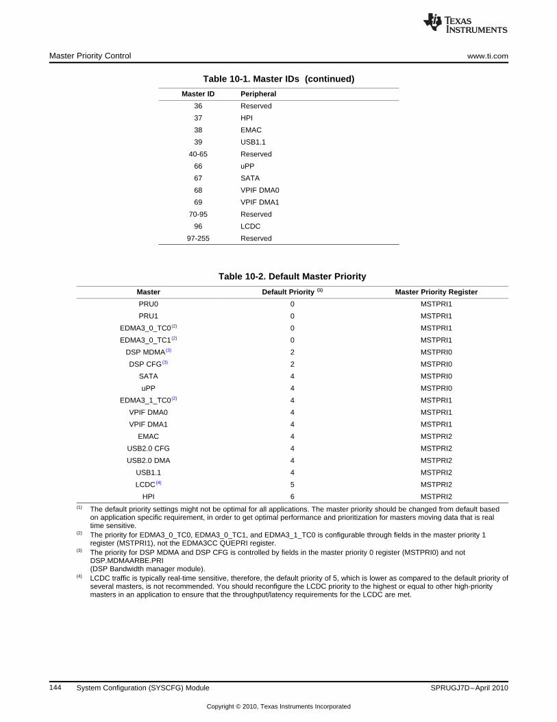
Master Priority Control www.ti.com
Table 10-1. Master IDs (continued)
Master ID Peripheral
36 Reserved
37 HPI
38 EMAC
39 USB1.1
40-65 Reserved
66 uPP
67 SATA
68 VPIF DMA0
69 VPIF DMA1
70-95 Reserved
96 LCDC
97-255 Reserved
Table 10-2. Default Master Priority
Master Default Priority (1) Master Priority Register
PRU0 0 MSTPRI1
PRU1 0 MSTPRI1
EDMA3_0_TC0 (2) 0 MSTPRI1
EDMA3_0_TC1 (2) 0 MSTPRI1
DSP MDMA (3) 2 MSTPRI0
DSP CFG (3) 2 MSTPRI0
SATA 4 MSTPRI0
uPP 4 MSTPRI0
EDMA3_1_TC0 (2) 4 MSTPRI1
VPIF DMA0 4 MSTPRI1
VPIF DMA1 4 MSTPRI1
EMAC 4 MSTPRI2
USB2.0 CFG 4 MSTPRI2
USB2.0 DMA 4 MSTPRI2
USB1.1 4 MSTPRI2
LCDC (4) 5 MSTPRI2
HPI 6 MSTPRI2(1) The default priority settings might not be optimal for all applications. The master priority should be changed from default based
on application specific requirement, in order to get optimal performance and prioritization for masters moving data that is realtime sensitive.
(2) The priority for EDMA3_0_TC0, EDMA3_0_TC1, and EDMA3_1_TC0 is configurable through fields in the master priority 1register (MSTPRI1), not the EDMA3CC QUEPRI register.
(3) The priority for DSP MDMA and DSP CFG is controlled by fields in the master priority 0 register (MSTPRI0) and notDSP.MDMAARBE.PRI(DSP Bandwidth manager module).
(4) LCDC traffic is typically real-time sensitive, therefore, the default priority of 5, which is lower as compared to the default priority ofseveral masters, is not recommended. You should reconfigure the LCDC priority to the highest or equal to other high-prioritymasters in an application to ensure that the throughput/latency requirements for the LCDC are met.
144 System Configuration (SYSCFG) Module SPRUGJ7D–April 2010
Copyright © 2010, Texas Instruments Incorporated

www.ti.com Host-DSP Communication Interrupts
10.4 Host-DSP Communication Interrupts
The SYSCFG module also has a set of registers to facilitate host-to-processor communication. This isgenerally used to allow an external host and the DSP to coordinate.
Either of the processors can set specific bits in this SYSCFG register, which in turn can interrupt the otherprocessor, if the interrupts have been appropriately enabled in the processor’s interrupt controller.
10.5 SYSCFG Registers
Table 10-3 lists the memory-mapped registers for the system configuration module 0 (SYSCFG0) andTable 10-4 lists the memory-mapped registers for the system configuration module 1 (SYSCFG1). Thesetables also indicate whether a particular register can be accessed only when the CPU is in privilegedmode.
Table 10-3. System Configuration Module 0 (SYSCFG0) Registers
Address Acronym Register Description Access Section
01C1 4000h REVID Revision Identification Register — Section 10.5.1
01C1 4008h DIEIDR0 (1) Die Identification Register 0 — —
01C1 400Ch DIEIDR1 (1) Die Identification Register 1 — —
01C1 4010h DIEIDR2 (1) Die Identification Register 2 — —
01C1 4014h DIEIDR3 (1) Die Identification Register 3 — —
01C1 4018h DEVIDR0 Device Identification Register 0 Privileged mode Section 10.5.2
01C1 4020h BOOTCFG Boot Configuration Register Privileged mode Section 10.5.3
01C1 4038h KICK0R Kick 0 Register Privileged mode Section 10.5.4.1
01C1 403Ch KICK1R Kick 1 Register Privileged mode Section 10.5.4.2
01C1 4044h HOST1CFG Host 1 Configuration Register — Section 10.5.5
01C1 40E0h IRAWSTAT Interrupt Raw Status/Set Register Privileged mode Section 10.5.6.1
01C1 40E4h IENSTAT Interrupt Enable Status/Clear Register Privileged mode Section 10.5.6.2
01C1 40E8h IENSET Interrupt Enable Register Privileged mode Section 10.5.6.3
01C1 40ECh IENCLR Interrupt Enable Clear Register Privileged mode Section 10.5.6.4
01C1 40F0h EOI End of Interrupt Register Privileged mode Section 10.5.6.5
01C1 40F4h FLTADDRR Fault Address Register Privileged mode Section 10.5.7.1
01C1 40F8h FLTSTAT Fault Status Register — Section 10.5.7.2
01C1 4110h MSTPRI0 Master Priority 0 Register Privileged mode Section 10.5.8.1
01C1 4114h MSTPRI1 Master Priority 1 Register Privileged mode Section 10.5.8.2
01C1 4118h MSTPRI2 Master Priority 2 Register Privileged mode Section 10.5.8.3
01C1 4120h PINMUX0 Pin Multiplexing Control 0 Register Privileged mode Section 10.5.9.1
01C1 4124h PINMUX1 Pin Multiplexing Control 1 Register Privileged mode Section 10.5.9.2
01C1 4128h PINMUX2 Pin Multiplexing Control 2 Register Privileged mode Section 10.5.9.3
01C1 412Ch PINMUX3 Pin Multiplexing Control 3 Register Privileged mode Section 10.5.9.4
01C1 4130h PINMUX4 Pin Multiplexing Control 4 Register Privileged mode Section 10.5.9.5
01C1 4134h PINMUX5 Pin Multiplexing Control 5 Register Privileged mode Section 10.5.9.6
01C1 4138h PINMUX6 Pin Multiplexing Control 6 Register Privileged mode Section 10.5.9.7
01C1 413Ch PINMUX7 Pin Multiplexing Control 7 Register Privileged mode Section 10.5.9.8
01C1 4140h PINMUX8 Pin Multiplexing Control 8 Register Privileged mode Section 10.5.9.9
01C1 4144h PINMUX9 Pin Multiplexing Control 9 Register Privileged mode Section 10.5.9.10
01C1 4148h PINMUX10 Pin Multiplexing Control 10 Register Privileged mode Section 10.5.9.11
01C1 414Ch PINMUX11 Pin Multiplexing Control 11 Register Privileged mode Section 10.5.9.12
01C1 4150h PINMUX12 Pin Multiplexing Control 12 Register Privileged mode Section 10.5.9.13
01C1 4154h PINMUX13 Pin Multiplexing Control 13 Register Privileged mode Section 10.5.9.14(1) This register is for internal-use only.
145SPRUGJ7D–April 2010 System Configuration (SYSCFG) Module
Copyright © 2010, Texas Instruments Incorporated

SYSCFG Registers www.ti.com
Table 10-3. System Configuration Module 0 (SYSCFG0) Registers (continued)
Address Acronym Register Description Access Section
01C1 4158h PINMUX14 Pin Multiplexing Control 14 Register Privileged mode Section 10.5.9.15
01C1 415Ch PINMUX15 Pin Multiplexing Control 15 Register Privileged mode Section 10.5.9.16
01C1 4160h PINMUX16 Pin Multiplexing Control 16 Register Privileged mode Section 10.5.9.17
01C1 4164h PINMUX17 Pin Multiplexing Control 17 Register Privileged mode Section 10.5.9.18
01C1 4168h PINMUX18 Pin Multiplexing Control 18 Register Privileged mode Section 10.5.9.19
01C1 416Ch PINMUX19 Pin Multiplexing Control 19 Register Privileged mode Section 10.5.9.20
01C1 4170h SUSPSRC Suspend Source Register Privileged mode Section 10.5.10
01C1 4174h CHIPSIG Chip Signal Register — Section 10.5.11
01C1 4178h CHIPSIG_CLR Chip Signal Clear Register — Section 10.5.12
01C1 417Ch CFGCHIP0 Chip Configuration 0 Register Privileged mode Section 10.5.13
01C1 4180h CFGCHIP1 Chip Configuration 1 Register Privileged mode Section 10.5.14
01C1 4184h CFGCHIP2 Chip Configuration 2 Register Privileged mode Section 10.5.15
01C1 4188h CFGCHIP3 Chip Configuration 3 Register Privileged mode Section 10.5.16
01C1 418Ch CFGCHIP4 Chip Configuration 4 Register Privileged mode Section 10.5.17
Table 10-4. System Configuration Module 1 (SYSCFG1) Registers
Address Acronym Register Description Access Section
01E2 C000h VTPIO_CTL VTP I/O Control Register Privileged mode Section 10.5.18
01E2 C004h DDR_SLEW DDR Slew Register Privileged mode Section 10.5.19
01E2 C008h DEEPSLEEP Deep Sleep Register Privileged mode Section 10.5.20
01E2 C00Ch PUPD_ENA Pullup/Pulldown Enable Register Privileged mode Section 10.5.21
01E2 C010h PUPD_SEL Pullup/Pulldown Selection Register Privileged mode Section 10.5.22
01E2 C014h RXACTIVE RXACTIVE Control Register Privileged mode Section 10.5.23
01E2 C018h PWRDN Power Down Control Register Privileged mode Section 10.5.24
146 System Configuration (SYSCFG) Module SPRUGJ7D–April 2010
Copyright © 2010, Texas Instruments Incorporated

www.ti.com SYSCFG Registers
10.5.1 Revision Identification Register (REVID)
The revision identification register (REVID) provides the revision information for the SYSCFG module. TheREVID is shown in Figure 10-1 and described in Table 10-5.
Figure 10-1. Revision Identification Register (REVID)31 0
REV
R-4E84 0102h
LEGEND: R = Read only; -n = value after reset
Table 10-5. Revision Identification Register (REVID) Field Descriptions
Bit Field Value Description
31-0 REV 4E84 0102h Revision ID. Revision information for the SYSCFG module.
10.5.2 Device Identification Register 0 (DEVIDR0)
The device identification register 0 (DEVIDR0) contains a software readable version of the JTAG IDdevice. Software can use this register to determine the version of the device on which it is executing. TheDEVIDR0 is shown in Figure 10-2 and described in Table 10-6.
Figure 10-2. Device Identification Register 0 (DEVIDR0)31 0
DEVID0
R-0B7D 102Fh
LEGEND: R = Read only; -n = value after reset
Table 10-6. Device Identification Register 0 (DEVIDR0) Field Descriptions
Bit Field Value Description
31-0 DEVID0 0B7D 102Fh Device identification.
147SPRUGJ7D–April 2010 System Configuration (SYSCFG) Module
Copyright © 2010, Texas Instruments Incorporated

SYSCFG Registers www.ti.com
10.5.3 Boot Configuration Register (BOOTCFG)
The device boot and configuration settings are latched at device reset, and captured in the bootconfiguration register (BOOTCFG). See the device-specific data manual and Chapter 11 for details onboot and configuration settings. The BOOTCFG is shown in Figure 10-3 and described in Table 10-7.
Figure 10-3. Boot Configuration Register (BOOTCFG)31 16
Reserved
R-0
15 0
BOOTMODE
R-0
LEGEND: R = Read only; -n = value after reset
Table 10-7. Boot Configuration Register (BOOTCFG) Field Descriptions
Bit Field Value Description
31-16 Reserved 0 Reserved
15-0 BOOTMODE 0-FFFFh Boot Mode. This reflects the state of the boot mode pins.
148 System Configuration (SYSCFG) Module SPRUGJ7D–April 2010
Copyright © 2010, Texas Instruments Incorporated
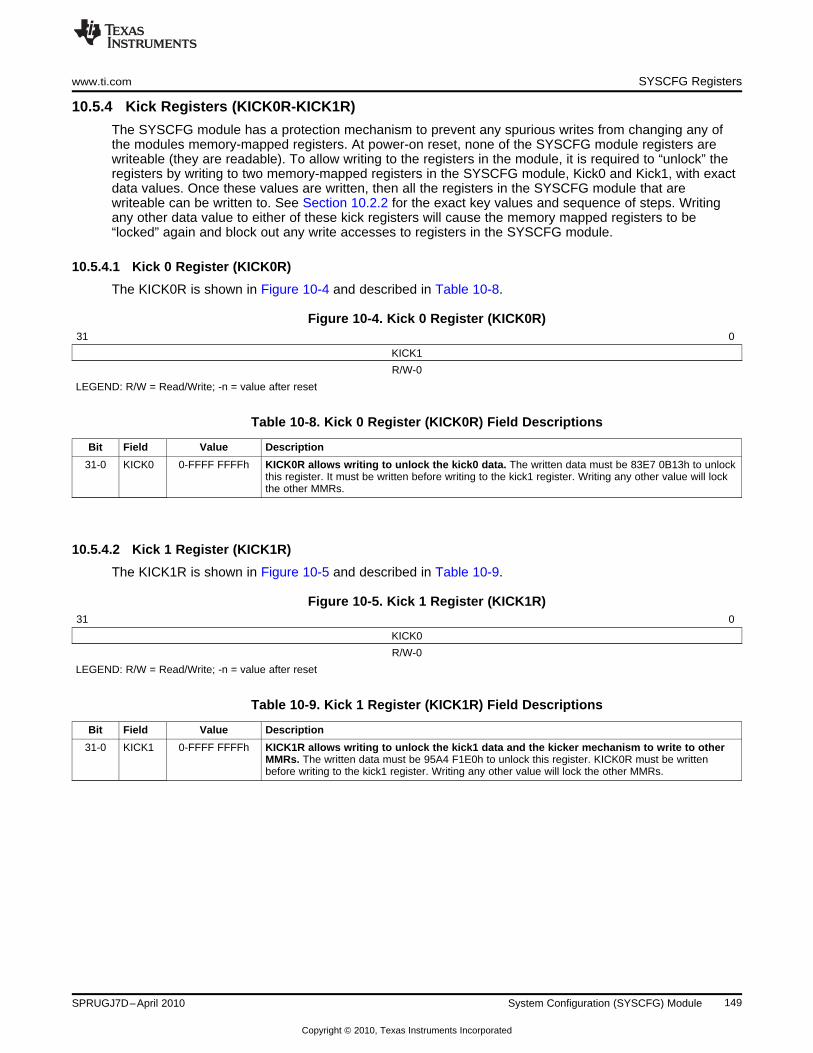
www.ti.com SYSCFG Registers
10.5.4 Kick Registers (KICK0R-KICK1R)
The SYSCFG module has a protection mechanism to prevent any spurious writes from changing any ofthe modules memory-mapped registers. At power-on reset, none of the SYSCFG module registers arewriteable (they are readable). To allow writing to the registers in the module, it is required to “unlock” theregisters by writing to two memory-mapped registers in the SYSCFG module, Kick0 and Kick1, with exactdata values. Once these values are written, then all the registers in the SYSCFG module that arewriteable can be written to. See Section 10.2.2 for the exact key values and sequence of steps. Writingany other data value to either of these kick registers will cause the memory mapped registers to be“locked” again and block out any write accesses to registers in the SYSCFG module.
10.5.4.1 Kick 0 Register (KICK0R)
The KICK0R is shown in Figure 10-4 and described in Table 10-8.
Figure 10-4. Kick 0 Register (KICK0R)31 0
KICK1
R/W-0
LEGEND: R/W = Read/Write; -n = value after reset
Table 10-8. Kick 0 Register (KICK0R) Field Descriptions
Bit Field Value Description
31-0 KICK0 0-FFFF FFFFh KICK0R allows writing to unlock the kick0 data. The written data must be 83E7 0B13h to unlockthis register. It must be written before writing to the kick1 register. Writing any other value will lockthe other MMRs.
10.5.4.2 Kick 1 Register (KICK1R)
The KICK1R is shown in Figure 10-5 and described in Table 10-9.
Figure 10-5. Kick 1 Register (KICK1R)31 0
KICK0
R/W-0
LEGEND: R/W = Read/Write; -n = value after reset
Table 10-9. Kick 1 Register (KICK1R) Field Descriptions
Bit Field Value Description
31-0 KICK1 0-FFFF FFFFh KICK1R allows writing to unlock the kick1 data and the kicker mechanism to write to otherMMRs. The written data must be 95A4 F1E0h to unlock this register. KICK0R must be writtenbefore writing to the kick1 register. Writing any other value will lock the other MMRs.
149SPRUGJ7D–April 2010 System Configuration (SYSCFG) Module
Copyright © 2010, Texas Instruments Incorporated

SYSCFG Registers www.ti.com
10.5.5 Host 1 Configuration Register (HOST1CFG)
The host 1 configuration register (HOST1CFG) provides information on the DSP boot address value atpower-on reset. The boot address defaults to 0070 0000h (DSP ROM) on power-up. The address field isread/writeable after reset and can be modified to allow execution from an alternate location after a modulelevel or local reset on the DSP. The HOST1CFG is shown in Figure 10-6 and described in Table 10-10.
Figure 10-6. Host 1 Configuration Register (HOST1CFG)31 16
DSP_ISTP_RST_VAL
R/W-0070h
15 10 9 0
DSP_ISTP_RST_VAL Reserved
R/W-0 R-0
LEGEND: R/W = Read/Write; R = Read only; -n = value after reset
Table 10-10. Host 1 Configuration Register (HOST1CFG) Field Descriptions
Bit Field Value Description
31-10 DSP_ISTP_RST_VAL 0-3F FFFFh DSP boot address vector.
9-0 Reserved 0 Reserved
150 System Configuration (SYSCFG) Module SPRUGJ7D–April 2010
Copyright © 2010, Texas Instruments Incorporated
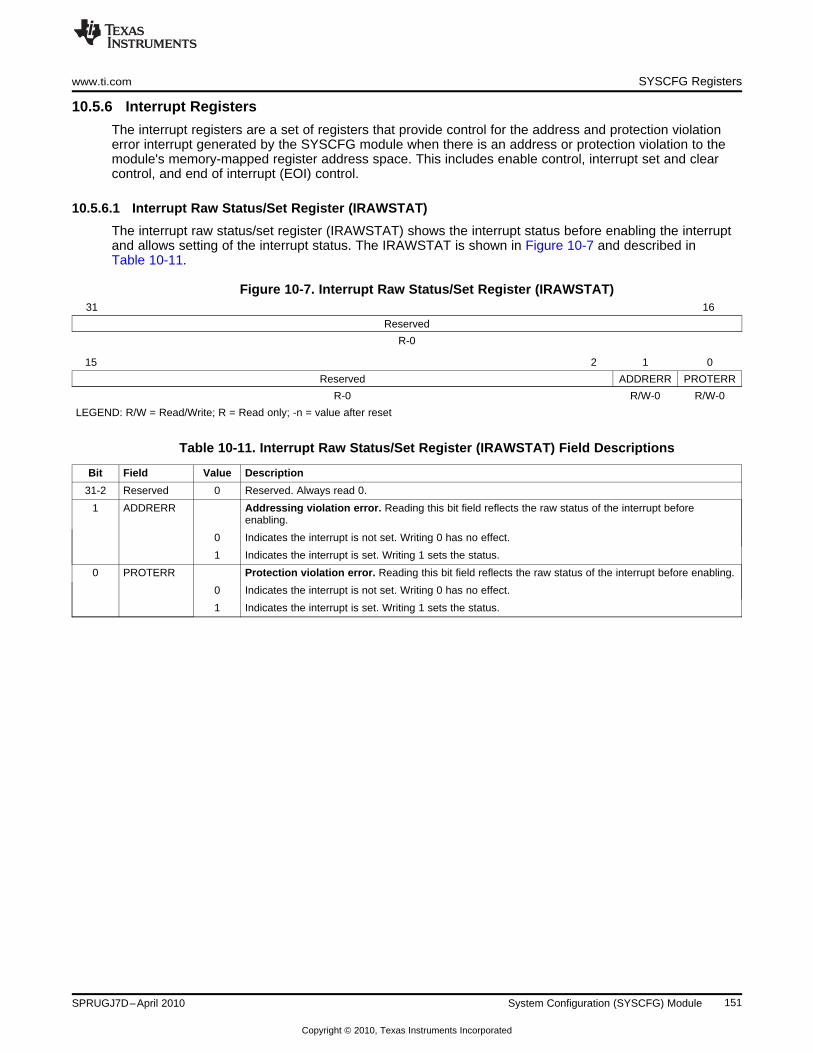
www.ti.com SYSCFG Registers
10.5.6 Interrupt Registers
The interrupt registers are a set of registers that provide control for the address and protection violationerror interrupt generated by the SYSCFG module when there is an address or protection violation to themodule's memory-mapped register address space. This includes enable control, interrupt set and clearcontrol, and end of interrupt (EOI) control.
10.5.6.1 Interrupt Raw Status/Set Register (IRAWSTAT)
The interrupt raw status/set register (IRAWSTAT) shows the interrupt status before enabling the interruptand allows setting of the interrupt status. The IRAWSTAT is shown in Figure 10-7 and described inTable 10-11.
Figure 10-7. Interrupt Raw Status/Set Register (IRAWSTAT)31 16
Reserved
R-0
15 2 1 0
Reserved ADDRERR PROTERR
R-0 R/W-0 R/W-0
LEGEND: R/W = Read/Write; R = Read only; -n = value after reset
Table 10-11. Interrupt Raw Status/Set Register (IRAWSTAT) Field Descriptions
Bit Field Value Description
31-2 Reserved 0 Reserved. Always read 0.
1 ADDRERR Addressing violation error. Reading this bit field reflects the raw status of the interrupt beforeenabling.
0 Indicates the interrupt is not set. Writing 0 has no effect.
1 Indicates the interrupt is set. Writing 1 sets the status.
0 PROTERR Protection violation error. Reading this bit field reflects the raw status of the interrupt before enabling.
0 Indicates the interrupt is not set. Writing 0 has no effect.
1 Indicates the interrupt is set. Writing 1 sets the status.
151SPRUGJ7D–April 2010 System Configuration (SYSCFG) Module
Copyright © 2010, Texas Instruments Incorporated

SYSCFG Registers www.ti.com
10.5.6.2 Interrupt Enable Status/Clear Register (IENSTAT)
The interrupt enable status/clear register (IENSTAT) shows the status of enabled interrupt and allowsclearing of the interrupt status. The IENSTAT is shown in Figure 10-8 and described in Table 10-12.
Figure 10-8. Interrupt Enable Status/Clear Register (IENSTAT)31 16
Reserved
R-0
15 2 1 0
Reserved ADDRERR PROTERR
R-0 R/W-0 R/W-0
LEGEND: R/W = Read/Write; R = Read only; -n = value after reset
Table 10-12. Interrupt Enable Status/Clear Register (IENSTAT) Field Descriptions
Bit Field Value Description
31-2 Reserved 0 Reserved. Always read 0.
1 ADDRERR Addressing violation error. Reading this bit field reflects the interrupt enabled status.
0 Indicates the interrupt is not set. Writing 0 has no effect.
1 Indicates the interrupt is set. Writing 1 clears the status.
0 PROTERR Protection violation error. Reading this bit field reflects the interrupt enabled status.
0 Indicates the interrupt is not set. Writing 0 has no effect.
1 Indicates the interrupt is set. Writing 1 clears the status.
152 System Configuration (SYSCFG) Module SPRUGJ7D–April 2010
Copyright © 2010, Texas Instruments Incorporated
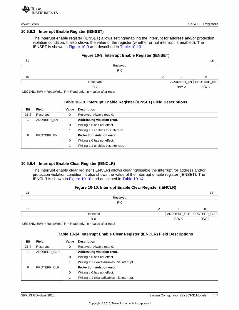
www.ti.com SYSCFG Registers
10.5.6.3 Interrupt Enable Register (IENSET)
The interrupt enable register (IENSET) allows setting/enabling the interrupt for address and/or protectionviolation condition. It also shows the value of the register (whether or not interrupt is enabled). TheIENSET is shown in Figure 10-9 and described in Table 10-13.
Figure 10-9. Interrupt Enable Register (IENSET)31 16
Reserved
R-0
15 2 1 0
Reserved ADDRERR_EN PROTERR_EN
R-0 R/W-0 R/W-0
LEGEND: R/W = Read/Write; R = Read only; -n = value after reset
Table 10-13. Interrupt Enable Register (IENSET) Field Descriptions
Bit Field Value Description
31-2 Reserved 0 Reserved. Always read 0.
1 ADDRERR_EN Addressing violation error.
0 Writing a 0 has not effect.
1 Writing a 1 enables this interrupt.
0 PROTERR_EN Protection violation error.
0 Writing a 0 has not effect.
1 Writing a 1 enables this interrupt.
10.5.6.4 Interrupt Enable Clear Register (IENCLR)
The interrupt enable clear register (IENCLR) allows clearing/disable the interrupt for address and/orprotection violation condition. It also shows the value of the interrupt enable register (IENSET). TheIENCLR is shown in Figure 10-10 and described in Table 10-14.
Figure 10-10. Interrupt Enable Clear Register (IENCLR)31 16
Reserved
R-0
15 2 1 0
Reserved ADDRERR_CLR PROTERR_CLR
R-0 R/W-0 R/W-0
LEGEND: R/W = Read/Write; R = Read only; -n = value after reset
Table 10-14. Interrupt Enable Clear Register (IENCLR) Field Descriptions
Bit Field Value Description
31-2 Reserved 0 Reserved. Always read 0.
1 ADDRERR_CLR Addressing violation error.
0 Writing a 0 has not effect.
1 Writing a 1 clears/disables this interrupt.
0 PROTERR_CLR Protection violation error.
0 Writing a 0 has not effect.
1 Writing a 1 clears/disables this interrupt.
153SPRUGJ7D–April 2010 System Configuration (SYSCFG) Module
Copyright © 2010, Texas Instruments Incorporated

SYSCFG Registers www.ti.com
10.5.6.5 End of Interrupt Register (EOI)
The end of interrupt register (EOI) is used in software to indicate completion of the interrupt servicing ofthe SYSCFG interrupt (for address/protection violation). You should write a value of 0 to the EOI registerbit 0 after the software has processed the SYSCFG interrupt, this acts as an acknowledgement ofcompletion of the SYSCFG interrupt so that the module can reliably generate the subsequent interrupts.The EOI is shown in Figure 10-11 and described in Table 10-15.
Figure 10-11. End of Interrupt Register (EOI)31 16
Reserved
R-0
15 8 7 0
Reserved EOIVECT
R-0 W-0
LEGEND: R = Read only; W = Write only; -n = value after reset
Table 10-15. End of Interrupt Register (EOI) Field Descriptions
Bit Field Value Description
31-8 Reserved 0 Reserved. Always read 0.
7-0 EOIVECT 0-FFh EOI vector value. Write the interrupt distribution value of the chip.
10.5.7 Fault Registers
The fault registers are a group of registers responsible for capturing the details on the faulty(address/protection violation errors) accesses, such as address and type of error.
10.5.7.1 Fault Address Register (FLTADDRR)
The fault address register (FLTADDRR) captures the address of the first transfer that causes the addressor memory violation error. The FLTADDRR is shown in Figure 10-12 and described in Table 10-16.
Figure 10-12. Fault Address Register (FLTADDRR)31 0
FLTADDR
R-0
LEGEND: R = Read only; -n = value after reset
Table 10-16. Fault Address Register (FLTADDRR) Field Descriptions
Bit Field Value Description
31-0 FLTADDR 0-FFFF FFFFh Fault address for the first fault transfer.
154 System Configuration (SYSCFG) Module SPRUGJ7D–April 2010
Copyright © 2010, Texas Instruments Incorporated

www.ti.com SYSCFG Registers
10.5.7.2 Fault Status Register (FLTSTAT)
The fault status register (FLTSTAT) holds/captures additional attributes and status of the first erroneoustransaction. This includes things like the master id for the master that caused the address/memoryviolation error, details on whether it is a user or supervisor level read/write or execute fault. The FLTSTATis shown in Figure 10-13 and described in Table 10-17.
Figure 10-13. Fault Status Register (FLTSTAT)31 24 23 16
ID MSTID
R-0 R-0
15 13 12 9 8 6 5 0
Reserved PRIVID Reserved TYPE
R-0 R-0 R-0 R-0
LEGEND: R = Read only; -n = value after reset
Table 10-17. Fault Status Register (FLTSTAT) Field Descriptions
Bit Field Value Description
31-24 ID 0-FFh Transfer ID of the first fault transfer.
23-16 MSTID 0-FFh Master ID of the first fault transfer.
15-13 Reserved 0 Reserved. Always read 0
12-9 PRIVID 0-Fh Privilege ID of the first fault transfer.
8-6 Reserved 0 Reserved. Always read 0
5-0 TYPE Fault type of first fault transfer.
0 No transfer fault
1h User execute fault
2h User write fault
3h Reserved
4h User read fault
5h-7h Reserved
8h Supervisor execute fault
9h-Fh Reserved
10h Supervisor write fault
11h-1Fh Reserved
20h Supervisor read fault
21h-3Fh Reserved
155SPRUGJ7D–April 2010 System Configuration (SYSCFG) Module
Copyright © 2010, Texas Instruments Incorporated

SYSCFG Registers www.ti.com
10.5.8 Master Priority Registers (MSTPRI0-MSTPRI2)
10.5.8.1 Master Priority 0 Register (MSTPRI0)
The master priority 0 register (MSTPRI0) is shown in Figure 10-14 and described in Table 10-18.
Figure 10-14. Master Priority 0 Register (MSTPRI0)31 30 28 27 26 24 23 22 20 19 18 16
Rsvd Reserved Rsvd Reserved Rsvd SATA Rsvd UPP
R/W-0 R/W-4h R/W-0 R/W-4h R/W-0 R/W-4h R/W-0 R/W-4h
15 14 12 11 10 8 7 6 4 3 2 0
Rsvd DSP_CFG Rsvd DSP_MDMA Rsvd Reserved Rsvd Reserved
R/W-0 R/W-2h R-0 R/W-2h R-0 R/W-2h R-0 R/W-2h
LEGEND: R/W = Read/Write; R = Read only; -n = value after reset
Table 10-18. Master Priority 0 Register (MSTPRI0) Field Descriptions
Bit Field Value Description
31 Reserved 0 Reserved. Write the default value when modifying this register.
30-28 Reserved 4h Reserved. Write the default value when modifying this register.
27 Reserved 0 Reserved. Write the default value when modifying this register.
26-24 Reserved 4h Reserved. Write the default value when modifying this register.
23 Reserved 0 Reserved. Write the default value when modifying this register.
22-20 SATA 0-7h SATA port priority. Bit = 0 = priority 0 (highest); bit = 7h = priority 7 (lowest).
19 Reserved 0 Reserved. Write the default value when modifying this register.
18-16 UPP 0-7h uPP port priority. Bit = 0 = priority 0 (highest); bit = 7h = priority 7 (lowest).
15 Reserved 0 Reserved. Write the default value when modifying this register.
14-12 DSP_CFG 0-7h DSP CFG port priority. Bit = 0 = priority 0 (highest); bit = 7h = priority 7 (lowest).
11 Reserved 0 Reserved. Always read as 0.
10-8 DSP_MDMA 0-7h DSP DMA port priority. Bit = 0 = priority 0 (highest); bit = 7h = priority 7 (lowest).
7 Reserved 0 Reserved. Always read as 0.
6-4 Reserved 2h Reserved. Write the default value when modifying this register.
3 Reserved 0 Reserved. Always read as 0.
2-0 Reserved 2h Reserved. Write the default value when modifying this register.
156 System Configuration (SYSCFG) Module SPRUGJ7D–April 2010
Copyright © 2010, Texas Instruments Incorporated

www.ti.com SYSCFG Registers
10.5.8.2 Master Priority 1 Register (MSTPRI1)
The master priority 1 register (MSTPRI1) is shown in Figure 10-15 and described in Table 10-19.
Figure 10-15. Master Priority 1 Register (MSTPRI1)31 30 28 27 26 24 23 22 20 19 18 16
Rsvd VPIF_DMA_1 Rsvd VPIF_DMA_0 Rsvd Reserved Rsvd EDMA31TC0
R/W-0 R/W-4h R/W-0 R/W-4h R/W-0 R/W-4h R/W-0 R/W-4h
15 14 12 11 10 8 7 6 4 3 2 0
Rsvd EDMA30TC1 Rsvd EDMA30TC0 Rsvd PRU1 Rsvd PRU0
R/W-0 R/W-0 R-0 R/W-0 R-0 R/W-0 R-0 R/W-0
LEGEND: R/W = Read/Write; R = Read only; -n = value after reset
Table 10-19. Master Priority 1 Register (MSTPRI1) Field Descriptions
Bit Field Value Description
31 Reserved 0 Reserved. Write the default value when modifying this register.
30-28 VPIF_DMA_1 0-7h VPIF DMA1 port priority. Bit = 0 = priority 0 (highest); bit = 7h = priority 7 (lowest).
27 Reserved 0 Reserved. Write the default value when modifying this register.
26-24 VPIF_DMA_0 0-7h VPIF DMA0 port priority. Bit = 0 = priority 0 (highest); bit = 7h = priority 7 (lowest).
23 Reserved 0 Reserved. Write the default value when modifying this register.
22-20 Reserved 4h Reserved. Write the default value when modifying this register.
19 Reserved 0 Reserved. Write the default value when modifying this register.
18-16 EDMA31TC0 0-7h EDMA3_1_TC0 port priority. Bit = 0 = priority 0 (highest); bit = 7h = priority 7 (lowest).
15 Reserved 0 Reserved. Write the default value when modifying this register.
14-12 EDMA30TC1 0-7h EDMA3_0_TC1 port priority. Bit = 0 = priority 0 (highest); bit = 7h = priority 7 (lowest).
11 Reserved 0 Reserved. Always read as 0.
10-8 EDMA30TC0 0-7h EDMA3_0_TC0 port priority. Bit = 0 = priority 0 (highest); bit = 7h = priority 7 (lowest).
7 Reserved 0 Reserved. Always read as 0.
6-4 PRU1 0-7h PRU1 port priority. Bit = 0 = priority 0 (highest); bit = 7h = priority 7 (lowest).
3 Reserved 0 Reserved. Always read as 0.
2-0 PRU0 0-7h PRU0 port priority. Bit = 0 = priority 0 (highest); bit = 7h = priority 7 (lowest).
157SPRUGJ7D–April 2010 System Configuration (SYSCFG) Module
Copyright © 2010, Texas Instruments Incorporated

SYSCFG Registers www.ti.com
10.5.8.3 Master Priority 2 Register (MSTPRI2)
The master priority 2 register (MSTPRI2) is shown in Figure 10-16 and described in Table 10-20.
Figure 10-16. Master Priority 2 Register (MSTPRI2)31 30 28 27 26 24 23 22 20 19 18 16
Rsvd LCDC Rsvd USB1 Rsvd UHPI Rsvd Reserved
R/W-0 R/W-5h R/W-0 R/W-4h R/W-0 R/W-6h R/W-0 R/W-0
15 14 12 11 10 8 7 6 4 3 2 0
Rsvd USB0CDMA Rsvd USB0CFG Rsvd Reserved Rsvd EMAC
R/W-0 R/W-4h R/W-0 R/W-4h R/W-0 R/W-0 R/W-0 R/W-4h
LEGEND: R/W = Read/Write; -n = value after reset
Table 10-20. Master Priority 2 Register (MSTPRI2) Field Descriptions
Bit Field Value Description
31 Reserved 0 Reserved. Write the default value when modifying this register.
30-28 LCDC 0-7h LCDC port priority. Bit = 0 = priority 0 (highest); bit = 7h = priority 7 (lowest).
27 Reserved 0 Reserved. Write the default value when modifying this register.
26-24 USB1 0-7h USB1 (USB1.1) port priority. Bit = 0 = priority 0 (highest); bit = 7h = priority 7 (lowest).
23 Reserved 0 Reserved. Write the default value when modifying this register.
22-20 UHPI 0-7h HPI port priority. Bit = 0 = priority 0 (highest); bit = 7h = priority 7 (lowest).
19 Reserved 0 Reserved. Write the default value when modifying this register.
18-16 Reserved 0 Reserved. Write the default value to all bits when modifying this register.
15 Reserved 0 Reserved. Write the default value when modifying this register.
14-12 USB0CDMA 0-7h USB0 (USB2.0) CDMA port priority. Bit = 0 = priority 0 (highest); bit = 7h = priority 7 (lowest).
11 Reserved 0 Reserved. Write the default value when modifying this register.
10-8 USB0CFG 0-7h USB0 (USB2.0) CFG port priority. Bit = 0 = priority 0 (highest); bit = 7h = priority 7 (lowest).
7 Reserved 0 Reserved. Write the default value to all bits when modifying this register.
6-4 Reserved 0 Reserved. Write the default value to all bits when modifying this register.
3 Reserved 0 Reserved. Write the default value when modifying this register.
2-0 EMAC 0-7h EMAC port priority. Bit = 0 = priority 0 (highest); bit = 7h = priority 7 (lowest).
158 System Configuration (SYSCFG) Module SPRUGJ7D–April 2010
Copyright © 2010, Texas Instruments Incorporated

www.ti.com SYSCFG Registers
10.5.9 Pin Multiplexing Control Registers (PINMUX0-PINMUX19)
Extensive use of pin multiplexing is used to accommodate the large number of peripheral functions in thesmallest possible package. On the device, pin multiplexing can be controlled on a pin by pin basis. This isdone by the pin multiplexing registers (PINMUX0-PINMUX19). Each pin that is multiplexed with severaldifferent functions has a corresponding 4-bit field in PINMUXn. Pin multiplexing selects which of severalperipheral pin functions control the pins I/O buffer output data and output enable values only. Note that theinput from each pin is always routed to all of the peripherals that share the pin; the PINMUX registershave no effect on input from a pin. Hardware does not attempt to ensure that the proper pin multiplexing isselected for the peripherals or that interface mode is being used. Detailed information about the pinmultiplexing and control is covered in the device-specific data manual. Access to the pin multiplexing utilityis available in OMAP-L1x8, TMS320C6742/6/8 Pin Multiplexing Utility Application Report (SPRAB63).
10.5.9.1 Pin Multiplexing Control 0 Register (PINMUX0)
Figure 10-17. Pin Multiplexing Control 0 Register (PINMUX0)31 28 27 24 23 20 19 16
PINMUX0_31_28 PINMUX0_27_24 PINMUX0_23_20 PINMUX0_19_16
R/W-0 R/W-0 R/W-0 R/W-0
15 12 11 8 7 4 3 0
PINMUX0_15_12 PINMUX0_11_8 PINMUX0_7_4 PINMUX0_3_0
R/W-0 R/W-0 R/W-0 R/W-0
LEGEND: R/W = Read/Write; -n = value after reset
Table 10-21. Pin Multiplexing Control 0 Register (PINMUX0) Field Descriptions
Bit Field Value Description
31-28 PINMUX0_31_28 DEEPSLEEP/RTC_ALARM/UART2_CTS/GP0[8] Control
0 Selects Function DEEPSLEEP
1h Reserved
2h Selects Function RTC_ALARM
3h Reserved
4h Selects Function UART2_CTS
5h-7h Reserved
8h Selects Function GP0[8]
9h-Fh Reserved
27-24 PINMUX0_27_24 PRU0_R31[16]/AMUTE/PRU0_R30[16]/UART2_RTS/GP0[9] Control
0 Selects Function PRU0_R31[16]
1h Selects Function AMUTE
2h Selects Function PRU0_R30[16]
3h Reserved
4h Selects Function UART2_RTS
5h-7h Reserved
8h Selects Function GP0[9]
9h-Fh Reserved
159SPRUGJ7D–April 2010 System Configuration (SYSCFG) Module
Copyright © 2010, Texas Instruments Incorporated

SYSCFG Registers www.ti.com
Table 10-21. Pin Multiplexing Control 0 Register (PINMUX0) Field Descriptions (continued)
Bit Field Value Description
23-20 PINMUX0_23_20 PRU0_R31[17]/AHCLKX/USB_REFCLKIN/UART1_CTS/GP0[10] Control
0 Selects Function PRU0_R31[17]
1h Selects Function AHCLKX
2h Selects Function USB_REFCLKIN
3h Reserved
4h Selects Function UART1_CTS
5h-7h Reserved
8h Selects Function GP0[10]
9h-Fh Reserved
19-16 PINMUX0_19_16 PRU0_R31[18]/AHCLKR/PRU0_R30[18]/UART1_RTS/GP0[11] Control
0 Selects Function PRU0_R31[18]
1h Selects Function AHCLKR
2h Selects Function PRU0_R30[18]
3h Reserved
4h Selects Function UART1_RTS
5h-7h Reserved
8h Selects Function GP0[11]
9h-Fh Reserved
15-12 PINMUX0_15_12 PRU0_R31[19]/AFSX/GP0[12] Control
0 Selects Function PRU0_R31[19]
1h Selects Function AFSX
2h-7h Reserved
8h Selects Function GP0[12]
9h-Fh Reserved
11-8 PINMUX0_11_8 PRU0_R31[20]/AFSR/GP0[13] Control
0 Selects Function PRU0_R31[20]
1h Selects Function AFSR
2h-7h Reserved
8h Selects Function GP0[13]
9h-Fh Reserved
7-4 PINMUX0_7_4 PRU0_R31[21]/ACLKX/PRU0_R30[19]/GP0[14] Control
0 Selects Function PRU0_R31[21]
1h Selects Function ACLKX
2h-3h Reserved
4h Selects Function PRU0_R30[19]
5h-7h Reserved
8h Selects Function GP0[14]
9h-Fh Reserved
3-0 PINMUX0_3_0 PRU0_R31[22]/ACLKR/PRU0_R30[20]/GP0[15] Control
0 Selects Function PRU0_R31[22]
1h Selects Function ACLKR
2h-3h Reserved
4h Selects Function PRU0_R30[20]
5h-7h Reserved
8h Selects Function GP0[15]
9h-Fh Reserved
160 System Configuration (SYSCFG) Module SPRUGJ7D–April 2010
Copyright © 2010, Texas Instruments Incorporated

www.ti.com SYSCFG Registers
10.5.9.2 Pin Multiplexing Control 1 Register (PINMUX1)
Figure 10-18. Pin Multiplexing Control 1 Register (PINMUX1)31 28 27 24 23 20 19 16
PINMUX1_31_28 PINMUX1_27_24 PINMUX1_23_20 PINMUX1_19_16
R/W-0 R/W-0 R/W-0 R/W-0
15 12 11 8 7 4 3 0
PINMUX1_15_12 PINMUX1_11_8 PINMUX1_7_4 PINMUX1_3_0
R/W-0 R/W-0 R/W-0 R/W-0
LEGEND: R/W = Read/Write; -n = value after reset
Table 10-22. Pin Multiplexing Control 1 Register (PINMUX1) Field Descriptions
Bit Field Value Description
31-28 PINMUX1_31_28 PRU0_R31[8]/AXR[8]/CLKS1/ECAP1_APWM1/GP0[0] Control
0 Selects Function PRU0_R31[8]
1h Selects Function AXR[8]
2h Selects Function CLKS1
3h Reserved
4h Selects Function ECAP1_APWM1
5h-7h Reserved
8h Selects Function GP0[0]
9h-Fh Reserved
27-24 PINMUX1_27_24 AXR[9]/DX1/GP0[1] Control
0 Pin is 3-stated.
1h Selects Function AXR[9]
2h Selects Function DX1
3h-7h Reserved
8h Selects Function GP0[1]
9h-Fh Reserved
23-20 PINMUX1_23_20 AXR[10]/DR1/GP0[2] Control
0 Pin is 3-stated.
1h Selects Function AXR[10]
2h Selects Function DR1
3h-7h Reserved
8h Selects Function GP0[2]
9h-Fh Reserved
19-16 PINMUX1_19_16 AXR[11]/FSX1/GP0[3] Control
0 Pin is 3-stated.
1h Selects Function AXR[11]
2h Selects Function FSX1
3h-7h Reserved
8h Selects Function GP0[3]
9h-Fh Reserved
161SPRUGJ7D–April 2010 System Configuration (SYSCFG) Module
Copyright © 2010, Texas Instruments Incorporated

SYSCFG Registers www.ti.com
Table 10-22. Pin Multiplexing Control 1 Register (PINMUX1) Field Descriptions (continued)
Bit Field Value Description
15-12 PINMUX1_15_12 AXR[12]/FSR1/GP0[4] Control
0 Pin is 3-stated.
1h Selects Function AXR[12]
2h Selects Function FSR1
3h-7h Reserved
8h Selects Function GP0[4]
9h-Fh Reserved
11-8 PINMUX1_11_8 AXR[13]/CLKX1/GP0[5] Control
0 Pin is 3-stated.
1h Selects Function AXR[13]
2h Selects Function CLKX1
3h-7h Reserved
8h Selects Function GP0[5]
9h-Fh Reserved
7-4 PINMUX1_7_4 AXR[14]/CLKR1/GP0[6] Control
0 Pin is 3-stated.
1h Selects Function AXR[14]
2h Selects Function CLKR1
3h-7h Reserved
8h Selects Function GP0[6]
9h-Fh Reserved
3-0 PINMUX1_3_0 AXR[15]/EPWM0TZ[0]/ECAP2_APWM2/GP0[7] Control
0 Pin is 3-stated.
1h Selects Function AXR[15]
2h Selects Function EPWM0TZ[0]
3h Reserved
4h Selects Function ECAP2_APWM2
5h-7h Reserved
8h Selects Function GP0[7]
9h-Fh Reserved
162 System Configuration (SYSCFG) Module SPRUGJ7D–April 2010
Copyright © 2010, Texas Instruments Incorporated

www.ti.com SYSCFG Registers
10.5.9.3 Pin Multiplexing Control 2 Register (PINMUX2)
Figure 10-19. Pin Multiplexing Control 2 Register (PINMUX2)31 28 27 24 23 20 19 16
PINMUX2_31_28 PINMUX2_27_24 PINMUX2_23_20 PINMUX2_19_16
R/W-0 R/W-0 R/W-0 R/W-0
15 12 11 8 7 4 3 0
PINMUX2_15_12 PINMUX2_11_8 PINMUX2_7_4 PINMUX2_3_0
R/W-0 R/W-0 R/W-0 R/W-0
LEGEND: R/W = Read/Write; -n = value after reset
Table 10-23. Pin Multiplexing Control 2 Register (PINMUX2) Field Descriptions
Bit Field Value Description
31-28 PINMUX2_31_28 CLKS0/AXR[0]/ECAP0_APWM0/GP8[7]/MII_TXD[0] Control
0 Selects Function CLKS0
1h Selects Function AXR[0]
2h Selects Function ECAP0_APWM0
3h Reserved
4h Selects Function GP8[7]
5h-7h Reserved
8h Selects Function MII_TXD[0]
9h-Fh Reserved
27-24 PINMUX2_27_24 AXR[1]/DX0/GP1[9]/MII_TXD[1] Control
0 Pin is 3-stated.
1h Selects Function AXR[1]
2h Selects Function DX0
3h Reserved
4h Selects Function GP1[9]
5h-7h Reserved
8h Selects Function MII_TXD[1]
9h-Fh Reserved
23-20 PINMUX2_23_20 AXR[2]/DR0/GP1[10]/MII_TXD[2] Control
0 Pin is 3-stated.
1h Selects Function AXR[2]
2h Selects Function DR0
3h Reserved
4h Selects Function GP1[10]
5h-7h Reserved
8h Selects Function MII_TXD[2]
9h-Fh Reserved
163SPRUGJ7D–April 2010 System Configuration (SYSCFG) Module
Copyright © 2010, Texas Instruments Incorporated

SYSCFG Registers www.ti.com
Table 10-23. Pin Multiplexing Control 2 Register (PINMUX2) Field Descriptions (continued)
Bit Field Value Description
19-16 PINMUX2_19_16 AXR[3]/FSX0/GP1[11]/MII_TXD[3] Control
0 Pin is 3-stated.
1h Selects Function AXR[3]
2h Selects Function FSX0
3h Reserved
4h Selects Function GP1[11]
5h-7h Reserved
8h Selects Function MII_TXD[3]
9h-Fh Reserved
15-12 PINMUX2_15_12 AXR[4]/FSR0/GP1[12]/MII_COL Control
0 Pin is 3-stated.
1h Selects Function AXR[4]
2h Selects Function FSR0
3h Reserved
4h Selects Function GP1[12]
5h-7h Reserved
8h Selects Function MII_COL
9h-Fh Reserved
11-8 PINMUX2_11_8 AXR[5]/CLKX0/GP1[13]/MII_TXCLK Control
0 Pin is 3-stated.
1h Selects Function AXR[5]
2h Selects Function CLKX0
3h Reserved
4h Selects Function GP1[13]
5h-7h Reserved
8h Selects Function MII_TXCLK
9h-Fh Reserved
7-4 PINMUX2_7_4 PRU0_R31[6]/AXR[6]/CLKR0/GP1[14]/MII_TXEN Control
0 Selects Function PRU0_R31[6]
1h Selects Function AXR[6]
2h Selects Function CLKR0
3h Reserved
4h Selects Function GP1[14]
5h-7h Reserved
8h Selects Function MII_TXEN
9h-Fh Reserved
3-0 PINMUX2_3_0 PRU0_R31[7]/AXR[7]/EPWM1TZ[0]/PRU0_R30[17]/GP1[15] Control
0 Selects Function PRU0_R31[7]
1h Selects Function AXR[7]
2h Selects Function EPWM1TZ[0]
3h Reserved
4h Selects Function PRU0_R30[17]
5h-7h Reserved
8h Selects Function GP1[15]
9h-Fh Reserved
164 System Configuration (SYSCFG) Module SPRUGJ7D–April 2010
Copyright © 2010, Texas Instruments Incorporated
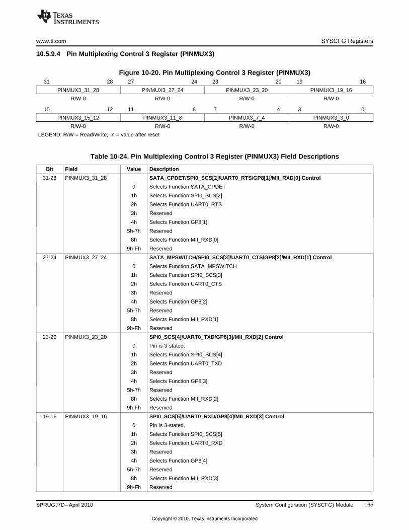
www.ti.com SYSCFG Registers
10.5.9.4 Pin Multiplexing Control 3 Register (PINMUX3)
Figure 10-20. Pin Multiplexing Control 3 Register (PINMUX3)31 28 27 24 23 20 19 16
PINMUX3_31_28 PINMUX3_27_24 PINMUX3_23_20 PINMUX3_19_16
R/W-0 R/W-0 R/W-0 R/W-0
15 12 11 8 7 4 3 0
PINMUX3_15_12 PINMUX3_11_8 PINMUX3_7_4 PINMUX3_3_0
R/W-0 R/W-0 R/W-0 R/W-0
LEGEND: R/W = Read/Write; -n = value after reset
Table 10-24. Pin Multiplexing Control 3 Register (PINMUX3) Field Descriptions
Bit Field Value Description
31-28 PINMUX3_31_28 SATA_CPDET/SPI0_SCS[2]/UART0_RTS/GP8[1]/MII_RXD[0] Control
0 Selects Function SATA_CPDET
1h Selects Function SPI0_SCS[2]
2h Selects Function UART0_RTS
3h Reserved
4h Selects Function GP8[1]
5h-7h Reserved
8h Selects Function MII_RXD[0]
9h-Fh Reserved
27-24 PINMUX3_27_24 SATA_MPSWITCH/SPI0_SCS[3]/UART0_CTS/GP8[2]/MII_RXD[1] Control
0 Selects Function SATA_MPSWITCH
1h Selects Function SPI0_SCS[3]
2h Selects Function UART0_CTS
3h Reserved
4h Selects Function GP8[2]
5h-7h Reserved
8h Selects Function MII_RXD[1]
9h-Fh Reserved
23-20 PINMUX3_23_20 SPI0_SCS[4]/UART0_TXD/GP8[3]/MII_RXD[2] Control
0 Pin is 3-stated.
1h Selects Function SPI0_SCS[4]
2h Selects Function UART0_TXD
3h Reserved
4h Selects Function GP8[3]
5h-7h Reserved
8h Selects Function MII_RXD[2]
9h-Fh Reserved
19-16 PINMUX3_19_16 SPI0_SCS[5]/UART0_RXD/GP8[4]/MII_RXD[3] Control
0 Pin is 3-stated.
1h Selects Function SPI0_SCS[5]
2h Selects Function UART0_RXD
3h Reserved
4h Selects Function GP8[4]
5h-7h Reserved
8h Selects Function MII_RXD[3]
9h-Fh Reserved
165SPRUGJ7D–April 2010 System Configuration (SYSCFG) Module
Copyright © 2010, Texas Instruments Incorporated

SYSCFG Registers www.ti.com
Table 10-24. Pin Multiplexing Control 3 Register (PINMUX3) Field Descriptions (continued)
Bit Field Value Description
15-12 PINMUX3_15_12 SPI0_SIMO/EPWMSYNCO/GP8[5]/MII_CRS Control
0 Pin is 3-stated.
1h Selects Function SPI0_SIMO
2h Selects Function EPWMSYNCO
3h Reserved
4h Selects Function GP8[5]
5h-7h Reserved
8h Selects Function MII_CRS
9h-Fh Reserved
11-8 PINMUX3_11_8 SPI0_SOMI/EPWMSYNCI/GP8[6]/MII_RXER Control
0 Pin is 3-stated.
1h Selects Function SPI0_SOMI
2h Selects Function EPWMSYNCI
3h Reserved
4h Selects Function GP8[6]
5h-7h Reserved
8h Selects Function MII_RXER
9h-Fh Reserved
7-4 PINMUX3_7_4 SPI0_ENA/EPWM0B/PRU0_R30[6]/MII_RXDV Control
0 Pin is 3-stated.
1h Selects Function SPI0_ENA
2h Selects Function EPWM0B
3h Reserved
4h Selects Function PRU0_R30[6]
5h-7h Reserved
8h Selects Function MII_RXDV
9h-Fh Reserved
3-0 PINMUX3_3_0 SPI0_CLK/EPWM0A/GP1[8]/MII_RXCLK Control
0 Pin is 3-stated.
1h Selects Function SPI0_CLK
2h Selects Function EPWM0A
3h Reserved
4h Selects Function GP1[8]
5h-7h Reserved
8h Selects Function MII_RXCLK
9h-Fh Reserved
166 System Configuration (SYSCFG) Module SPRUGJ7D–April 2010
Copyright © 2010, Texas Instruments Incorporated

www.ti.com SYSCFG Registers
10.5.9.5 Pin Multiplexing Control 4 Register (PINMUX4)
Figure 10-21. Pin Multiplexing Control 4 Register (PINMUX4)31 28 27 24 23 20 19 16
PINMUX4_31_28 PINMUX4_27_24 PINMUX4_23_20 PINMUX4_19_16
R/W-0 R/W-0 R/W-0 R/W-0
15 12 11 8 7 4 3 0
PINMUX4_15_12 PINMUX4_11_8 PINMUX4_7_4 PINMUX4_3_0
R/W-0 R/W-0 R/W-0 R/W-0
LEGEND: R/W = Read/Write; -n = value after reset
Table 10-25. Pin Multiplexing Control 4 Register (PINMUX4) Field Descriptions
Bit Field Value Description
31-28 PINMUX4_31_28 SP1_SCS[2]/UART1_TXD/SATA_CPPOD/GP1[0] Control
0 Pin is 3-stated.
1h Selects Function SP1_SCS[2]
2h Selects Function UART1_TXD
3h Reserved
4h Selects Function SATA_CPPOD
5h-7h Reserved
8h Selects Function GP1[0]
9h-Fh Reserved
27-24 PINMUX4_27_24 SPI1_SCS[3]/UART1_RXD/SATA_LED/GP1[1] Control
0 Pin is 3-stated.
1h Selects Function SPI1_SCS[3]
2h Selects Function UART1_RXD
3h Reserved
4h Selects Function SATA_LED
5h-7h Reserved
8h Selects Function GP1[1]
9h-Fh Reserved
23-20 PINMUX4_23_20 SPI1_SCS[4]/UART2_TXD/I2C1_SDA/GP1[2] Control
0 Pin is 3-stated.
1h Selects Function SPI1_SCS[4]
2h Selects Function UART2_TXD
3h Reserved
4h Selects Function I2C1_SDA
5h-7h Reserved
8h Selects Function GP1[2]
9h-Fh Reserved
19-16 PINMUX4_19_16 SPI1_SCS[5]/UART2_RXD/I2C1_SCL/GP1[3] Control
0 Pin is 3-stated.
1h Selects Function SPI1_SCS[5]
2h Selects Function UART2_RXD
3h Reserved
4h Selects Function I2C1_SCL
5h-7h Reserved
8h Selects Function GP1[3]
9h-Fh Reserved
167SPRUGJ7D–April 2010 System Configuration (SYSCFG) Module
Copyright © 2010, Texas Instruments Incorporated
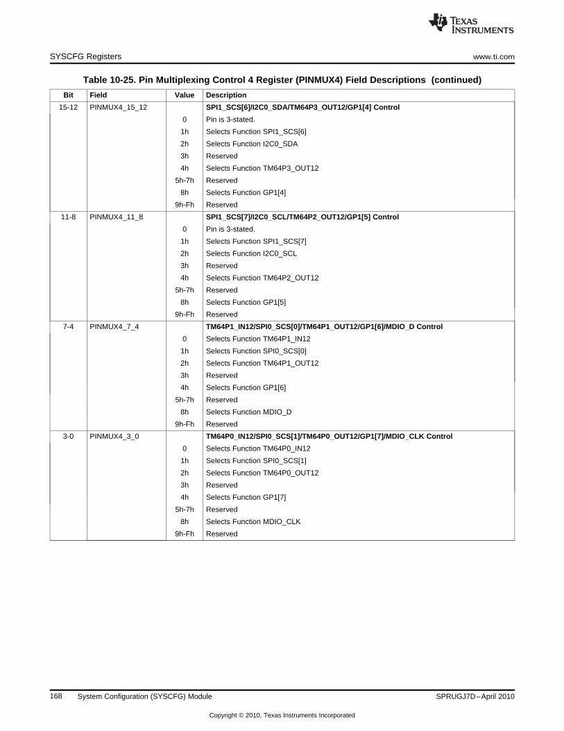
SYSCFG Registers www.ti.com
Table 10-25. Pin Multiplexing Control 4 Register (PINMUX4) Field Descriptions (continued)
Bit Field Value Description
15-12 PINMUX4_15_12 SPI1_SCS[6]/I2C0_SDA/TM64P3_OUT12/GP1[4] Control
0 Pin is 3-stated.
1h Selects Function SPI1_SCS[6]
2h Selects Function I2C0_SDA
3h Reserved
4h Selects Function TM64P3_OUT12
5h-7h Reserved
8h Selects Function GP1[4]
9h-Fh Reserved
11-8 PINMUX4_11_8 SPI1_SCS[7]/I2C0_SCL/TM64P2_OUT12/GP1[5] Control
0 Pin is 3-stated.
1h Selects Function SPI1_SCS[7]
2h Selects Function I2C0_SCL
3h Reserved
4h Selects Function TM64P2_OUT12
5h-7h Reserved
8h Selects Function GP1[5]
9h-Fh Reserved
7-4 PINMUX4_7_4 TM64P1_IN12/SPI0_SCS[0]/TM64P1_OUT12/GP1[6]/MDIO_D Control
0 Selects Function TM64P1_IN12
1h Selects Function SPI0_SCS[0]
2h Selects Function TM64P1_OUT12
3h Reserved
4h Selects Function GP1[6]
5h-7h Reserved
8h Selects Function MDIO_D
9h-Fh Reserved
3-0 PINMUX4_3_0 TM64P0_IN12/SPI0_SCS[1]/TM64P0_OUT12/GP1[7]/MDIO_CLK Control
0 Selects Function TM64P0_IN12
1h Selects Function SPI0_SCS[1]
2h Selects Function TM64P0_OUT12
3h Reserved
4h Selects Function GP1[7]
5h-7h Reserved
8h Selects Function MDIO_CLK
9h-Fh Reserved
168 System Configuration (SYSCFG) Module SPRUGJ7D–April 2010
Copyright © 2010, Texas Instruments Incorporated

www.ti.com SYSCFG Registers
10.5.9.6 Pin Multiplexing Control 5 Register (PINMUX5)
Figure 10-22. Pin Multiplexing Control 5 Register (PINMUX5)31 28 27 24 23 20 19 16
PINMUX5_31_28 PINMUX5_27_24 PINMUX5_23_20 PINMUX5_19_16
R/W-0 R/W-0 R/W-0 R/W-0
15 12 11 8 7 4 3 0
PINMUX5_15_12 PINMUX5_11_8 PINMUX5_7_4 PINMUX5_3_0
R/W-0 R/W-0 R/W-0 R/W-0
LEGEND: R/W = Read/Write; -n = value after reset
Table 10-26. Pin Multiplexing Control 5 Register (PINMUX5) Field Descriptions
Bit Field Value Description
31-28 PINMUX5_31_28 EMA_BA[0]/GP2[8] Control
0 Pin is 3-stated.
1h Selects Function EMA_BA[0]
2h-7h Reserved
8h Selects Function GP2[8]
9h-Fh Reserved
27-24 PINMUX5_27_24 EMA_BA[1]/GP2[9] Control
0 Pin is 3-stated.
1h Selects Function EMA_BA[1]
2h-7h Reserved
8h Selects Function GP2[9]
9h-Fh Reserved
23-20 PINMUX5_23_20 SPI1_SIMO/GP2[10] Control
0 Pin is 3-stated.
1h Selects Function SPI1_SIMO
2h-7h Reserved
8h Selects Function GP2[10]
9h-Fh Reserved
19-16 PINMUX5_19_16 SPI1_SOMI/GP2[11] Control
0 Pin is 3-stated.
1h Selects Function SPI1_SOMI
2h-7h Reserved
8h Selects Function GP2[11]
9h-Fh Reserved
15-12 PINMUX5_15_12 SPI1_ENA/GP2[12] Control
0 Pin is 3-stated.
1h Selects Function SPI1_ENA
2h-7h Reserved
8h Selects Function GP2[12]
9h-Fh Reserved
11-8 PINMUX5_11_8 SPI1_CLK/GP2[13] Control
0 Pin is 3-stated.
1h Selects Function SPI1_CLK
2h-7h Reserved
8h Selects Function GP2[13]
9h-Fh Reserved
169SPRUGJ7D–April 2010 System Configuration (SYSCFG) Module
Copyright © 2010, Texas Instruments Incorporated

SYSCFG Registers www.ti.com
Table 10-26. Pin Multiplexing Control 5 Register (PINMUX5) Field Descriptions (continued)
Bit Field Value Description
7-4 PINMUX5_7_4 TM64P3_IN12/SPI1_SCS[0]/EPWM1B/PRU0_R30[7]/GP2[14] Control
0 Selects Function TM64P3_IN12
1h Selects Function SPI1_SCS[0]
2h Selects Function EPWM1B
3h Reserved
4h Selects Function PRU0_R30[7]
5h-7h Reserved
8h Selects Function GP2[14]
9h-Fh Reserved
3-0 PINMUX5_3_0 TM64P2_IN12/SPI1_SCS[1]/EPWM1A/PRU0_R30[8]/GP2[15] Control
0 Selects Function TM64P2_IN12
1h Selects Function SPI1_SCS[1]
2h Selects Function EPWM1A
3h Reserved
4h Selects Function PRU0_R30[8]
5h-7h Reserved
8h Selects Function GP2[15]
9h-Fh Reserved
170 System Configuration (SYSCFG) Module SPRUGJ7D–April 2010
Copyright © 2010, Texas Instruments Incorporated

www.ti.com SYSCFG Registers
10.5.9.7 Pin Multiplexing Control 6 Register (PINMUX6)
Figure 10-23. Pin Multiplexing Control 6 Register (PINMUX6)31 28 27 24 23 20 19 16
PINMUX6_31_28 PINMUX6_27_24 PINMUX6_23_20 PINMUX6_19_16
R/W-0 R/W-0 R/W-0 R/W-0
15 12 11 8 7 4 3 0
PINMUX6_15_12 PINMUX6_11_8 PINMUX6_7_4 PINMUX6_3_0
R/W-0 R/W-0 R/W-0 R/W-0
LEGEND: R/W = Read/Write; -n = value after reset
Table 10-27. Pin Multiplexing Control 6 Register (PINMUX6) Field Descriptions
Bit Field Value Description
31-28 PINMUX6_31_28 EMA_CS[0]/GP2[0] Control
0 Pin is 3-stated.
1h Selects Function EMA_CS[0]
2h-7h Reserved
8h Selects Function GP2[0]
9h-Fh Reserved
27-24 PINMUX6_27_24 PRU0_R31[1]/EMA_WAIT[1]/PRU0_R30[1]/GP2[1] Control
0 Selects Function PRU0_R31[1]
1h Selects Function EMA_WAIT[1]
2h-3h Reserved
4h Selects Function PRU0_R30[1]
5h-7h Reserved
8h Selects Function GP2[1]
9h-Fh Reserved
23-20 PINMUX6_23_20 EMA_WE_DQM[1]/GP2[2] Control
0 Pin is 3-stated.
1h Selects Function EMA_WE_DQM[1]
2h-7h Reserved
8h Selects Function GP2[2]
9h-Fh Reserved
19-16 PINMUX6_19_16 EMA_WE_DQM[0]/GP2[3] Control
0 Pin is 3-stated.
1h Selects Function EMA_WE_DQM[0]
2h-7h Reserved
8h Selects Function GP2[3]
9h-Fh Reserved
15-12 PINMUX6_15_12 PRU0_R31[2]/EMA_CAS/PRU0_R30[2]/GP2[4] Control
0 Selects Function PRU0_R31[2]
1h Selects Function EMA_CAS
2h-3h Reserved
4h Selects Function PRU0_R30[2]
5h-7h Reserved
8h Selects Function GP2[4]
9h-Fh Reserved
171SPRUGJ7D–April 2010 System Configuration (SYSCFG) Module
Copyright © 2010, Texas Instruments Incorporated

SYSCFG Registers www.ti.com
Table 10-27. Pin Multiplexing Control 6 Register (PINMUX6) Field Descriptions (continued)
Bit Field Value Description
11-8 PINMUX6_11_8 PRU0_R31[3]/EMA_RAS/PRU0_R30[3]/GP2[5] Control
0 Selects Function PRU0_R31[3]
1h Selects Function EMA_RAS
2h-3h Reserved
4h Selects Function PRU0_R30[3]
5h-7h Reserved
8h Selects Function GP2[5]
9h-Fh Reserved
7-4 PINMUX6_7_4 PRU0_R31[4]/EMA_SDCKE/PRU0_R30[4]/GP2[6] Control
0 Selects Function PRU0_R31[4]
1h Selects Function EMA_SDCKE
2h-3h Reserved
4h Selects Function PRU0_R30[4]
5h-7h Reserved
8h Selects Function GP2[6]
9h-Fh Reserved
3-0 PINMUX6_3_0 PRU0_R31[5]/EMA_CLK/PRU0_R30[5]/GP2[7] Control
0 Selects Function PRU0_R31[5]
1h Selects Function EMA_CLK
2h-3h Reserved
4h Selects Function PRU0_R30[5]
5h-7h Reserved
8h Selects Function GP2[7]
9h-Fh Reserved
172 System Configuration (SYSCFG) Module SPRUGJ7D–April 2010
Copyright © 2010, Texas Instruments Incorporated

www.ti.com SYSCFG Registers
10.5.9.8 Pin Multiplexing Control 7 Register (PINMUX7)
Figure 10-24. Pin Multiplexing Control 7 Register (PINMUX7)31 28 27 24 23 20 19 16
PINMUX7_31_28 PINMUX7_27_24 PINMUX7_23_20 PINMUX7_19_16
R/W-0 R/W-0 R/W-0 R/W-0
15 12 11 8 7 4 3 0
PINMUX7_15_12 PINMUX7_11_8 PINMUX7_7_4 PINMUX7_3_0
R/W-0 R/W-0 R/W-0 R/W-0
LEGEND: R/W = Read/Write; -n = value after reset
Table 10-28. Pin Multiplexing Control 7 Register (PINMUX7) Field Descriptions
Bit Field Value Description
31-28 PINMUX7_31_28 PRU0_R31[0]/EMA_WAIT[0]/PRU0_R30[0]/GP3[8] Control
0 Selects Function PRU0_R31[0]
1h Selects Function EMA_WAIT[0]
2h-3h Reserved
4h Selects Function PRU0_R30[0]
5h-7h Reserved
8h Selects Function GP3[8]
9h-Fh Reserved
27-24 PINMUX7_27_24 EMA_RNW/GP3[9] Control
0 Pin is 3-stated.
1h Selects Function EMA_RNW
2h-7h Reserved
8h Selects Function GP3[9]
9h-Fh Reserved
23-20 PINMUX7_23_20 EMA_OE/GP3[10] Control
0 Pin is 3-stated.
1h Selects Function EMA_OE
2h-7h Reserved
8h Selects Function GP3[10]
9h-Fh Reserved
19-16 PINMUX7_19_16 EMA_WE/GP3[11] Control
0 Pin is 3-stated.
1h Selects Function EMA_WE
2h-7h Reserved
8h Selects Function GP3[11]
9h-Fh Reserved
15-12 PINMUX7_15_12 EMA_CS[5]/GP3[12] Control
0 Pin is 3-stated.
1h Selects Function EMA_CS[5]
2h-7h Reserved
8h Selects Function GP3[12]
9h-Fh Reserved
173SPRUGJ7D–April 2010 System Configuration (SYSCFG) Module
Copyright © 2010, Texas Instruments Incorporated

SYSCFG Registers www.ti.com
Table 10-28. Pin Multiplexing Control 7 Register (PINMUX7) Field Descriptions (continued)
Bit Field Value Description
11-8 PINMUX7_11_8 EMA_CS[4]/GP3[13] Control
0 Pin is 3-stated.
1h Selects Function EMA_CS[4]
2h-7h Reserved
8h Selects Function GP3[13]
9h-Fh Reserved
7-4 PINMUX7_7_4 EMA_CS[3]/GP3[14] Control
0 Pin is 3-stated.
1h Selects Function EMA_CS[3]
2h-7h Reserved
8h Selects Function GP3[14]
9h-Fh Reserved
3-0 PINMUX7_3_0 EMA_CS[2]/GP3[15] Control
0 Pin is 3-stated.
1h Selects Function EMA_CS[2]
2h-7h Reserved
8h Selects Function GP3[15]
9h-Fh Reserved
174 System Configuration (SYSCFG) Module SPRUGJ7D–April 2010
Copyright © 2010, Texas Instruments Incorporated

www.ti.com SYSCFG Registers
10.5.9.9 Pin Multiplexing Control 8 Register (PINMUX8)
Figure 10-25. Pin Multiplexing Control 8 Register (PINMUX8)31 28 27 24 23 20 19 16
PINMUX8_31_28 PINMUX8_27_24 PINMUX8_23_20 PINMUX8_19_16
R/W-0 R/W-0 R/W-0 R/W-0
15 12 11 8 7 4 3 0
PINMUX8_15_12 PINMUX8_11_8 PINMUX8_7_4 PINMUX8_3_0
R/W-0 R/W-0 R/W-0 R/W-0
LEGEND: R/W = Read/Write; -n = value after reset
Table 10-29. Pin Multiplexing Control 8 Register (PINMUX8) Field Descriptions
Bit Field Value Description
31-28 PINMUX8_31_28 EMA_D[8]/GP3[0] Control
0 Pin is 3-stated.
1h Selects Function EMA_D[8]
2h-7h Reserved
8h Selects Function GP3[0]
9h-Fh Reserved
27-24 PINMUX8_27_24 EMA_D[9]/GP3[1] Control
0 Pin is 3-stated.
1h Selects Function EMA_D[9]
2h-7h Reserved
8h Selects Function GP3[1]
9h-Fh Reserved
23-20 PINMUX8_23_20 EMA_D[10]/GP3[2] Control
0 Pin is 3-stated.
1h Selects Function EMA_D[10]
2h-7h Reserved
8h Selects Function GP3[2]
9h-Fh Reserved
19-16 PINMUX8_19_16 EMA_D[11]/GP3[3] Control
0 Pin is 3-stated.
1h Selects Function EMA_D[11]
2h-7h Reserved
8h Selects Function GP3[3]
9h-Fh Reserved
15-12 PINMUX8_15_12 EMA_D[12]/GP3[4] Control
0 Pin is 3-stated.
1h Selects Function EMA_D[12]
2h-7h Reserved
8h Selects Function GP3[4]
9h-Fh Reserved
11-8 PINMUX8_11_8 EMA_D[13]/GP3[5] Control
0 Pin is 3-stated.
1h Selects Function EMA_D[13]
2h-7h Reserved
8h Selects Function GP3[5]
9h-Fh Reserved
175SPRUGJ7D–April 2010 System Configuration (SYSCFG) Module
Copyright © 2010, Texas Instruments Incorporated

SYSCFG Registers www.ti.com
Table 10-29. Pin Multiplexing Control 8 Register (PINMUX8) Field Descriptions (continued)
Bit Field Value Description
7-4 PINMUX8_7_4 EMA_D[14]/GP3[6] Control
0 Pin is 3-stated.
1h Selects Function EMA_D[14]
2h-7h Reserved
8h Selects Function GP3[6]
9h-Fh Reserved
3-0 PINMUX8_3_0 EMA_D[15]/GP3[7] Control
0 Pin is 3-stated.
1h Selects Function EMA_D[15]
2h-7h Reserved
8h Selects Function GP3[7]
9h-Fh Reserved
176 System Configuration (SYSCFG) Module SPRUGJ7D–April 2010
Copyright © 2010, Texas Instruments Incorporated

www.ti.com SYSCFG Registers
10.5.9.10 Pin Multiplexing Control 9 Register (PINMUX9)
Figure 10-26. Pin Multiplexing Control 9 Register (PINMUX9)31 28 27 24 23 20 19 16
PINMUX9_31_28 PINMUX9_27_24 PINMUX9_23_20 PINMUX9_19_16
R/W-0 R/W-0 R/W-0 R/W-0
15 12 11 8 7 4 3 0
PINMUX9_15_12 PINMUX9_11_8 PINMUX9_7_4 PINMUX9_3_0
R/W-0 R/W-0 R/W-0 R/W-0
LEGEND: R/W = Read/Write; -n = value after reset
Table 10-30. Pin Multiplexing Control 9 Register (PINMUX9) Field Descriptions
Bit Field Value Description
31-28 PINMUX9_31_28 EMA_D[0]/GP4[8] Control
0 Pin is 3-stated.
1h Selects Function EMA_D[0]
2h-7h Reserved
8h Selects Function GP4[8]
9h-Fh Reserved
27-24 PINMUX9_27_24 EMA_D[1]/GP4[9] Control
0 Pin is 3-stated.
1h Selects Function EMA_D[1]
2h-7h Reserved
8h Selects Function GP4[9]
9h-Fh Reserved
23-20 PINMUX9_23_20 EMA_D[2]/GP4[10] Control
0 Pin is 3-stated.
1h Selects Function EMA_D[2]
2h-7h Reserved
8h Selects Function GP4[10]
9h-Fh Reserved
19-16 PINMUX9_19_16 EMA_D[3]/GP4[11] Control
0 Pin is 3-stated.
1h Selects Function EMA_D[3]
2h-7h Reserved
8h Selects Function GP4[11]
9h-Fh Reserved
15-12 PINMUX9_15_12 EMA_D[4]/GP4[12] Control
0 Pin is 3-stated.
1h Selects Function EMA_D[4]
2h-7h Reserved
8h Selects Function GP4[12]
9h-Fh Reserved
11-8 PINMUX9_11_8 EMA_D[5]/GP4[13] Control
0 Pin is 3-stated.
1h Selects Function EMA_D[5]
2h-7h Reserved
8h Selects Function GP4[13]
9h-Fh Reserved
177SPRUGJ7D–April 2010 System Configuration (SYSCFG) Module
Copyright © 2010, Texas Instruments Incorporated

SYSCFG Registers www.ti.com
Table 10-30. Pin Multiplexing Control 9 Register (PINMUX9) Field Descriptions (continued)
Bit Field Value Description
7-4 PINMUX9_7_4 EMA_D[6]/GP4[14] Control
0 Pin is 3-stated.
1h Selects Function EMA_D[6]
2h-7h Reserved
8h Selects Function GP4[14]
9h-Fh Reserved
3-0 PINMUX9_3_0 EMA_D[7]/GP4[15] Control
0 Pin is 3-stated.
1h Selects Function EMA_D[7]
2h-7h Reserved
8h Selects Function GP4[15]
9h-Fh Reserved
178 System Configuration (SYSCFG) Module SPRUGJ7D–April 2010
Copyright © 2010, Texas Instruments Incorporated

www.ti.com SYSCFG Registers
10.5.9.11 Pin Multiplexing Control 10 Register (PINMUX10)
Figure 10-27. Pin Multiplexing Control 10 Register (PINMUX10)31 28 27 24 23 20 19 16
PINMUX10_31_28 PINMUX10_27_24 PINMUX10_23_20 PINMUX10_19_16
R/W-0 R/W-0 R/W-0 R/W-0
15 12 11 8 7 4 3 0
PINMUX10_15_12 PINMUX10_11_8 PINMUX10_7_4 PINMUX10_3_0
R/W-0 R/W-0 R/W-0 R/W-0
LEGEND: R/W = Read/Write; -n = value after reset
Table 10-31. Pin Multiplexing Control 10 Register (PINMUX10) Field Descriptions
Bit Field Value Description
31-28 PINMUX10_31_28 EMA_A[16]/MMCSD0_DAT[5]/PRU1_R30[24]/GP4[0] Control
0 Pin is 3-stated.
1h Selects Function EMA_A[16]
2h Selects Function MMCSD0_DAT[5]
3h Reserved
4h Selects Function PRU1_R30[24]
5h-7h Reserved
8h Selects Function GP4[0]
9h-Fh Reserved
27-24 PINMUX10_27_24 EMA_A[17]/MMCSD0_DAT[4]/PRU1_R30[25]/GP4[1] Control
0 Pin is 3-stated.
1h Selects Function EMA_A[17]
2h Selects Function MMCSD0_DAT[4]
3h Reserved
4h Selects Function PRU1_R30[25]
5h-7h Reserved
8h Selects Function GP4[1]
9h-Fh Reserved
23-20 PINMUX10_23_20 EMA_A[18]/MMCSD0_DAT[3]/PRU1_R30[26]/GP4[2] Control
0 Pin is 3-stated.
1h Selects Function EMA_A[18]
2h Selects Function MMCSD0_DAT[3]
3h Reserved
4h Selects Function PRU1_R30[26]
5h-7h Reserved
8h Selects Function GP4[2]
9h-Fh Reserved
179SPRUGJ7D–April 2010 System Configuration (SYSCFG) Module
Copyright © 2010, Texas Instruments Incorporated

SYSCFG Registers www.ti.com
Table 10-31. Pin Multiplexing Control 10 Register (PINMUX10) Field Descriptions (continued)
Bit Field Value Description
19-16 PINMUX10_19_16 EMA_A[19]/MMCSD0_DAT[2]/PRU1_R30[27]/GP4[3] Control
0 Pin is 3-stated.
1h Selects Function EMA_A[19]
2h Selects Function MMCSD0_DAT[2]
3h Reserved
4h Selects Function PRU1_R30[27]
5h-7h Reserved
8h Selects Function GP4[3]
9h-Fh Reserved
15-12 PINMUX10_15_12 EMA_A[20]/MMCSD0_DAT[1]/PRU1_R30[28]/GP4[4] Control
0 Pin is 3-stated.
1h Selects Function EMA_A[20]
2h Selects Function MMCSD0_DAT[1]
3h Reserved
4h Selects Function PRU1_R30[28]
5h-7h Reserved
8h Selects Function GP4[4]
9h-Fh Reserved
11-8 PINMUX10_11_8 EMA_A[21]/MMCSD0_DAT[0]/PRU1_R30[29]/GP4[5] Control
0 Pin is 3-stated.
1h Selects Function EMA_A[21]
2h Selects Function MMCSD0_DAT[0]
3h Reserved
4h Selects Function PRU1_R30[29]
5h-7h Reserved
8h Selects Function GP4[5]
9h-Fh Reserved
7-4 PINMUX10_7_4 EMA_A[22]/MMCSD0_CMD/PRU1_R30[30]/GP4[6] Control
0 Pin is 3-stated.
1h Selects Function EMA_A[22]
2h Selects Function MMCSD0_CMD
3h Reserved
4h Selects Function PRU1_R30[30]
5h-7h Reserved
8h Selects Function GP4[6]
9h-Fh Reserved
3-0 PINMUX10_3_0 MMCSD0_CLK/PRU1_R30[31]/GP4[7] Control
0 Pin is 3-stated.
1h Reserved
2h Selects Function MMCSD0_CLK
3h Reserved
4h Selects Function PRU1_R30[31]
5h-7h Reserved
8h Selects Function GP4[7]
9h-Fh Reserved
180 System Configuration (SYSCFG) Module SPRUGJ7D–April 2010
Copyright © 2010, Texas Instruments Incorporated

www.ti.com SYSCFG Registers
10.5.9.12 Pin Multiplexing Control 11 Register (PINMUX11)
Figure 10-28. Pin Multiplexing Control 11 Register (PINMUX11)31 28 27 24 23 20 19 16
PINMUX11_31_28 PINMUX11_27_24 PINMUX11_23_20 PINMUX11_19_16
R/W-0 R/W-0 R/W-0 R/W-0
15 12 11 8 7 4 3 0
PINMUX11_15_12 PINMUX11_11_8 PINMUX11_7_4 PINMUX11_3_0
R/W-0 R/W-0 R/W-0 R/W-0
LEGEND: R/W = Read/Write; -n = value after reset
Table 10-32. Pin Multiplexing Control 11 Register (PINMUX11) Field Descriptions
Bit Field Value Description
31-28 PINMUX11_31_28 EMA_A[8]/PRU1_R30[16]/GP5[8] Control
0 Pin is 3-stated.
1h Selects Function EMA_A[8]
2h-3h Reserved
4h Selects Function PRU1_R30[16]
5h-7h Reserved
8h Selects Function GP5[8]
9h-Fh Reserved
27-24 PINMUX11_27_24 EMA_A[9]/PRU1_R30[17]/GP5[9] Control
0 Pin is 3-stated.
1h Selects Function EMA_A[9]
2h-3h Reserved
4h Selects Function PRU1_R30[17]
5h-7h Reserved
8h Selects Function GP5[9]
9h-Fh Reserved
23-20 PINMUX11_23_20 PRU1_R31[18]/EMA_A[10]/PRU1_R30[18]/GP5[10] Control
0 Selects Function PRU1_R31[18]
1h Selects Function EMA_A[10]
2h-3h Reserved
4h Selects Function PRU1_R30[18]
5h-7h Reserved
8h Selects Function GP5[10]
9h-Fh Reserved
19-16 PINMUX11_19_16 PRU1_R31[19]/EMA_A[11]/PRU1_R30[19]/GP5[11] Control
0 Selects Function PRU1_R31[19]
1h Selects Function EMA_A[11]
2h-3h Reserved
4h Selects Function PRU1_R30[19]
5h-7h Reserved
8h Selects Function GP5[11]
9h-Fh Reserved
181SPRUGJ7D–April 2010 System Configuration (SYSCFG) Module
Copyright © 2010, Texas Instruments Incorporated

SYSCFG Registers www.ti.com
Table 10-32. Pin Multiplexing Control 11 Register (PINMUX11) Field Descriptions (continued)
Bit Field Value Description
15-12 PINMUX11_15_12 PRU1_R31[20]/EMA_A[12]/PRU1_R30[20]/GP5[12] Control
0 Selects Function PRU1_R31[20]
1h Selects Function EMA_A[12]
2h-3h Reserved
4h Selects Function PRU1_R30[20]
5h-7h Reserved
8h Selects Function GP5[12]
9h-Fh Reserved
11-8 PINMUX11_11_8 PRU1_R31[21]/EMA_A[13]/PRU0_R30[21]/PRU1_R30[21]/GP5[13] Control
0 Selects Function PRU1_R31[21]
1h Selects Function EMA_A[13]
2h Selects Function PRU0_R30[21]
3h Reserved
4h Selects Function PRU1_R30[21]
5h-7h Reserved
8h Selects Function GP5[13]
9h-Fh Reserved
7-4 PINMUX11_7_4 PRU1_R31[22]/EMA_A[14]/MMCSD0_DAT[7]/PRU1_R30[22]/GP5[14] Control
0 Selects Function PRU1_R31[22]
1h Selects Function EMA_A[14]
2h Selects Function MMCSD0_DAT[7]
3h Reserved
4h Selects Function PRU1_R30[22]
5h-7h Reserved
8h Selects Function GP5[14]
9h-Fh Reserved
3-0 PINMUX11_3_0 PRU1_R31[23]/EMA_A[15]/MMCSD0_DAT[6]/PRU1_R30[23]/GP5[15] Control
0 Selects Function PRU1_R31[23]
1h Selects Function EMA_A[15]
2h Selects Function MMCSD0_DAT[6]
3h Reserved
4h Selects Function PRU1_R30[23]
5h-7h Reserved
8h Selects Function GP5[15]
9h-Fh Reserved
182 System Configuration (SYSCFG) Module SPRUGJ7D–April 2010
Copyright © 2010, Texas Instruments Incorporated

www.ti.com SYSCFG Registers
10.5.9.13 Pin Multiplexing Control 12 Register (PINMUX12)
Figure 10-29. Pin Multiplexing Control 12 Register (PINMUX12)31 28 27 24 23 20 19 16
PINMUX12_31_28 PINMUX12_27_24 PINMUX12_23_20 PINMUX12_19_16
R/W-0 R/W-0 R/W-0 R/W-0
15 12 11 8 7 4 3 0
PINMUX12_15_12 PINMUX12_11_8 PINMUX12_7_4 PINMUX12_3_0
R/W-0 R/W-0 R/W-0 R/W-0
LEGEND: R/W = Read/Write; -n = value after reset
Table 10-33. Pin Multiplexing Control 12 Register (PINMUX12) Field Descriptions
Bit Field Value Description
31-28 PINMUX12_31_28 EMA_A[0]/GP5[0] Control
0 Pin is 3-stated.
1h Selects Function EMA_A[0]
2h-7h Reserved
8h Selects Function GP5[0]
9h-Fh Reserved
27-24 PINMUX12_27_24 EMA_A[1]/GP5[1] Control
0 Pin is 3-stated.
1h Selects Function EMA_A[1]
2h-7h Reserved
8h Selects Function GP5[1]
9h-Fh Reserved
23-20 PINMUX12_23_20 EMA_A[2]/GP5[2] Control
0 Pin is 3-stated.
1h Selects Function EMA_A[2]
2h-7h Reserved
8h Selects Function GP5[2]
9h-Fh Reserved
19-16 PINMUX12_19_16 EMA_A[3]/GP5[3] Control
0 Pin is 3-stated.
1h Selects Function EMA_A[3]
2h-7h Reserved
8h Selects Function GP5[3]
9h-Fh Reserved
15-12 PINMUX12_15_12 EMA_A[4]/GP5[4] Control
0 Pin is 3-stated.
1h Selects Function EMA_A[4]
2h-7h Reserved
8h Selects Function GP5[4]
9h-Fh Reserved
11-8 PINMUX12_11_8 EMA_A[5]/GP5[5] Control
0 Pin is 3-stated.
1h Selects Function EMA_A[5]
2h-7h Reserved
8h Selects Function GP5[5]
9h-Fh Reserved
183SPRUGJ7D–April 2010 System Configuration (SYSCFG) Module
Copyright © 2010, Texas Instruments Incorporated

SYSCFG Registers www.ti.com
Table 10-33. Pin Multiplexing Control 12 Register (PINMUX12) Field Descriptions (continued)
Bit Field Value Description
7-4 PINMUX12_7_4 EMA_A[6]/GP5[6] Control
0 Pin is 3-stated.
1h Selects Function EMA_A[6]
2h-7h Reserved
8h Selects Function GP5[6]
9h-Fh Reserved
3-0 PINMUX12_3_0 EMA_A[7]/PRU1_R30[15]/GP5[7] Control
0 Pin is 3-stated.
1h Selects Function EMA_A[7]
2h-3h Reserved
4h Selects Function PRU1_R30[15]
5h-7h Reserved
8h Selects Function GP5[7]
9h-Fh Reserved
184 System Configuration (SYSCFG) Module SPRUGJ7D–April 2010
Copyright © 2010, Texas Instruments Incorporated

www.ti.com SYSCFG Registers
10.5.9.14 Pin Multiplexing Control 13 Register (PINMUX13)
Figure 10-30. Pin Multiplexing Control 13 Register (PINMUX13)31 28 27 24 23 20 19 16
PINMUX13_31_28 PINMUX13_27_24 PINMUX13_23_20 PINMUX13_19_16
R/W-0 R/W-0 R/W-0 R/W-0
15 12 11 8 7 4 3 0
PINMUX13_15_12 PINMUX13_11_8 PINMUX13_7_4 PINMUX13_3_0
R/W-0 R/W-0 R/W-0 R/W-0
LEGEND: R/W = Read/Write; -n = value after reset
Table 10-34. Pin Multiplexing Control 13 Register (PINMUX13) Field Descriptions
Bit Field Value Description
31-28 PINMUX13_31_28 PRU1_R31[17]/PRU0_R30[26]/UHPI_HRnW/UPP_CH1_WAIT/GP6[8] Control
0 Selects Function PRU1_R31[17]
1h Selects Function PRU0_R30[26]
2h Selects Function UHPI_HRnW
3h Reserved
4h Selects Function UPP_CH1_WAIT
5h-7h Reserved
8h Selects Function GP6[8]
9h-Fh Reserved
27-24 PINMUX13_27_24 PRU0_R30[27]/UHPI_HHWIL/UPP_CH1_ENABLE/GP6[9] Control
0 Pin is 3-stated.
1h Selects Function PRU0_R30[27]
2h Selects Function UHPI_HHWIL
3h Reserved
4h Selects Function UPP_CH1_ENABLE
5h-7h Reserved
8h Selects Function GP6[9]
9h-Fh Reserved
23-20 PINMUX13_23_20 PRU0_R30[28]/UHPI_HCNTL1/UPP_CH1_START/GP6[10] Control
0 Pin is 3-stated.
1h Selects Function PRU0_R30[28]
2h Selects Function UHPI_HCNTL1
3h Reserved
4h Selects Function UPP_CH1_START
5h-7h Reserved
8h Selects Function GP6[10]
9h-Fh Reserved
185SPRUGJ7D–April 2010 System Configuration (SYSCFG) Module
Copyright © 2010, Texas Instruments Incorporated

SYSCFG Registers www.ti.com
Table 10-34. Pin Multiplexing Control 13 Register (PINMUX13) Field Descriptions (continued)
Bit Field Value Description
19-16 PINMUX13_19_16 PRU0_R30[29]/UHPI_HCNTL0/UPP_CH1_CLK/GP6[11] Control
0 Pin is 3-stated.
1h Selects Function PRU0_R30[29]
2h Selects Function UHPI_HCNTL0
3h Reserved
4h Selects Function UPP_CH1_CLK
5h-7h Reserved
8h Selects Function GP6[11]
9h-Fh Reserved
15-12 PINMUX13_15_12 PRU0_R30[30]/UHPI_HINT/PRU1_R30[11]/GP6[12] Control
0 Pin is 3-stated.
1h Selects Function PRU0_R30[30]
2h Selects Function UHPI_HINT
3h Reserved
4h Selects Function PRU1_R30[11]
5h-7h Reserved
8h Selects Function GP6[12]
9h-Fh Reserved
11-8 PINMUX13_11_8 PRU0_R30[31]/UHPI_HRDY/PRU1_R30[12]/GP6[13] Control
0 Pin is 3-stated.
1h Selects Function PRU0_R30[31]
2h Selects Function UHPI_HRDY
3h Reserved
4h Selects Function PRU1_R30[12]
5h-7h Reserved
8h Selects Function GP6[13]
9h-Fh Reserved
7-4 PINMUX13_7_4 OBSCLK0/UHPI_HDS2/PRU1_R30[13]/GP6[14] Control
0 Pin is 3-stated.
1h Selects Function OBSCLK0
2h Selects Function UHPI_HDS2
3h Reserved
4h Selects Function PRU1_R30[13]
5h-7h Reserved
8h Selects Function GP6[14]
9h-Fh Reserved
3-0 PINMUX13_3_0 RESETOUT/UHPI_HAS/PRU1_R30[14]/GP6[15] Control
0 Selects Function RESETOUT
1h Selects Function RESETOUT
2h Selects Function UHPI_HAS
3h Reserved
4h Selects Function PRU1_R30[14]
5h-7h Reserved
8h Selects Function GP6[15]
9h-Fh Reserved
186 System Configuration (SYSCFG) Module SPRUGJ7D–April 2010
Copyright © 2010, Texas Instruments Incorporated

www.ti.com SYSCFG Registers
10.5.9.15 Pin Multiplexing Control 14 Register (PINMUX14)
Figure 10-31. Pin Multiplexing Control 14 Register (PINMUX14)31 28 27 24 23 20 19 16
PINMUX14_31_28 PINMUX14_27_24 PINMUX14_23_20 PINMUX14_19_16
R/W-0 R/W-0 R/W-0 R/W-0
15 12 11 8 7 4 3 0
PINMUX14_15_12 PINMUX14_11_8 PINMUX14_7_4 PINMUX14_3_0
R/W-0 R/W-0 R/W-0 R/W-0
LEGEND: R/W = Read/Write; -n = value after reset
Table 10-35. Pin Multiplexing Control 14 Register (PINMUX14) Field Descriptions
Bit Field Value Description
31-28 PINMUX14_31_28 PRU0_R31[24]/VPIF_DIN2/UHPI_HD[10]/UPP_D10/RMII_RXER Control
0 Selects Function PRU0_R31[24]
1h Selects Function VPIF_DIN2
2h Selects Function UHPI_HD[10]
3h Reserved
4h Selects Function UPP_D10
5h-7h Reserved
8h Selects Function RMII_RXER
9h-Fh Reserved
27-24 PINMUX14_27_24 PRU0_R31[25]/VPIF_DIN3/UHPI_HD[11]/UPP_D11/RMII_RXD[0] Control
0 Selects Function PRU0_R31[25]
1h Selects Function VPIF_DIN3
2h Selects Function UHPI_HD[11]
3h Reserved
4h Selects Function UPP_D11
5h-7h Reserved
8h Selects Function RMII_RXD[0]
9h-Fh Reserved
23-20 PINMUX14_23_20 PRU0_R31[26]/VPIF_DIN4/UHPI_HD[12]/UPP_D12/RMII_RXD[1] Control
0 Selects Function PRU0_R31[26]
1h Selects Function VPIF_DIN4
2h Selects Function UHPI_HD[12]
3h Reserved
4h Selects Function UPP_D12
5h-7h Reserved
8h Selects Function RMII_RXD[1]
9h-Fh Reserved
187SPRUGJ7D–April 2010 System Configuration (SYSCFG) Module
Copyright © 2010, Texas Instruments Incorporated

SYSCFG Registers www.ti.com
Table 10-35. Pin Multiplexing Control 14 Register (PINMUX14) Field Descriptions (continued)
Bit Field Value Description
19-16 PINMUX14_19_16 PRU0_R31[27]/VPIF_DIN5/UHPI_HD[13]/UPP_D13/RMII_TXEN Control
0 Selects Function PRU0_R31[27]
1h Selects Function VPIF_DIN5
2h Selects Function UHPI_HD[13]
3h Reserved
4h Selects Function UPP_D13
5h-7h Reserved
8h Selects Function RMII_TXEN
9h-Fh Reserved
15-12 PINMUX14_15_12 PRU0_R31[28]/VPIF_DIN6/UHPI_HD[14]/UPP_D14/RMII_TXD[0] Control
0 Selects Function PRU0_R31[28]
1h Selects Function VPIF_DIN6
2h Selects Function UHPI_HD[14]
3h Reserved
4h Selects Function UPP_D14
5h-7h Reserved
8h Selects Function RMII_TXD[0]
9h-Fh Reserved
11-8 PINMUX14_11_8 PRU0_R31[29]/VPIF_DIN7/UHPI_HD[15]/UPP_D15/RMII_TXD[1] Control
0 Selects Function PRU0_R31[29]
1h Selects Function VPIF_DIN7
2h Selects Function UHPI_HD[15]
3h Reserved
4h Selects Function UPP_D15
5h-7h Reserved
8h Selects Function RMII_TXD[1]
9h-Fh Reserved
7-4 PINMUX14_7_4 PRU1_R31[16]/VPIF_CLKIN1/UHPI_HDS1/PRU1_R30[9]/GP6[6] Control
0 Selects Function PRU1_R31[16]
1h Selects Function VPIF_CLKIN1
2h Selects Function UHPI_HDS1
3h Reserved
4h Selects Function PRU1_R30[9]
5h-7h Reserved
8h Selects Function GP6[6]
9h-Fh Reserved
3-0 PINMUX14_3_0 UPP_2xTXCLK/VPIF_CLKIN0/UHPI_HCS/PRU1_R30[10]/GP6[7] Control
0 Selects Function UPP_2xTXCLK
1h Selects Function VPIF_CLKIN0
2h Selects Function UHPI_HCS
3h Reserved
4h Selects Function PRU1_R30[10]
5h-7h Reserved
8h Selects Function GP6[7]
9h-Fh Reserved
188 System Configuration (SYSCFG) Module SPRUGJ7D–April 2010
Copyright © 2010, Texas Instruments Incorporated

www.ti.com SYSCFG Registers
10.5.9.16 Pin Multiplexing Control 15 Register (PINMUX15)
Figure 10-32. Pin Multiplexing Control 15 Register (PINMUX15)31 28 27 24 23 20 19 16
PINMUX15_31_28 PINMUX15_27_24 PINMUX15_23_20 PINMUX15_19_16
R/W-0 R/W-0 R/W-0 R/W-0
15 12 11 8 7 4 3 0
PINMUX15_15_12 PINMUX15_11_8 PINMUX15_7_4 PINMUX15_3_0
R/W-0 R/W-0 R/W-0 R/W-0
LEGEND: R/W = Read/Write; -n = value after reset
Table 10-36. Pin Multiplexing Control 15 Register (PINMUX15) Field Descriptions
Bit Field Value Description
31-28 PINMUX15_31_28 PRU0_R31[10]/VPIF_DIN10/UHPI_HD[2]/UPP_D2/PRU0_R30[10] Control
0 Selects Function PRU0_R31[10]
1h Selects Function VPIF_DIN10
2h Selects Function UHPI_HD[2]
3h Reserved
4h Selects Function UPP_D2
5h-7h Reserved
8h Selects Function PRU0_R30[10]
9h-Fh Reserved
27-24 PINMUX15_27_24 PRU0_R31[11]/VPIF_DIN11/UHPI_HD[3]/UPP_D3/PRU0_R30[11] Control
0 Selects Function PRU0_R31[11]
1h Selects Function VPIF_DIN11
2h Selects Function UHPI_HD[3]
3h Reserved
4h Selects Function UPP_D3
5h-7h Reserved
8h Selects Function PRU0_R30[11]
9h-Fh Reserved
23-20 PINMUX15_23_20 PRU0_R31[12]/VPIF_DIN12/UHPI_HD[4]/UPP_D4/PRU0_R30[12] Control
0 Selects Function PRU0_R31[12]
1h Selects Function VPIF_DIN12
2h Selects Function UHPI_HD[4]
3h Reserved
4h Selects Function UPP_D4
5h-7h Reserved
8h Selects Function PRU0_R30[12]
9h-Fh Reserved
189SPRUGJ7D–April 2010 System Configuration (SYSCFG) Module
Copyright © 2010, Texas Instruments Incorporated

SYSCFG Registers www.ti.com
Table 10-36. Pin Multiplexing Control 15 Register (PINMUX15) Field Descriptions (continued)
Bit Field Value Description
19-16 PINMUX15_19_16 PRU0_R31[13]/VPIF_DIN13_FIELD/UHPI_HD[5]/UPP_D5/PRU0_R30[13] Control
0 Selects Function PRU0_R31[13]
1h Selects Function VPIF_DIN13_FIELD
2h Selects Function UHPI_HD[5]
3h Reserved
4h Selects Function UPP_D5
5h-7h Reserved
8h Selects Function PRU0_R30[13]
9h-Fh Reserved
15-12 PINMUX15_15_12 PRU0_R31[14]/VPIF_DIN14_HSYNC/UHPI_HD[6]/UPP_D6/PRU0_R30[14] Control
0 Selects Function PRU0_R31[14]
1h Selects Function VPIF_DIN14_HSYNC
2h Selects Function UHPI_HD[6]
3h Reserved
4h Selects Function UPP_D6
5h-7h Reserved
8h Selects Function PRU0_R30[14]
9h-Fh Reserved
11-8 PINMUX15_11_8 PRU0_R31[15]/VPIF_DIN15_VSYNC/UHPI_HD[7]/UPP_D7/PRU0_R30[15] Control
0 Selects Function PRU0_R31[15]
1h Selects Function VPIF_DIN15_VSYNC
2h Selects Function UHPI_HD[7]
3h Reserved
4h Selects Function UPP_D7
5h-7h Reserved
8h Selects Function PRU0_R30[15]
9h-Fh Reserved
7-4 PINMUX15_7_4 PRU1_R31[29]/VPIF_DIN0/UHPI_HD[8]/UPP_D8/RMII_CRS_DV Control
0 Selects Function PRU1_R31[29]
1h Selects Function VPIF_DIN0
2h Selects Function UHPI_HD[8]
3h Reserved
4h Selects Function UPP_D8
5h-7h Reserved
8h Selects Function RMII_CRS_DV
9h-Fh Reserved
3-0 PINMUX15_3_0 PRU0_R31[23]/VPIF_DIN1/UHPI_HD[9]/UPP_D9/RMII_MHZ_50_CLK Control
0 Selects Function PRU0_R31[23]
1h Selects Function VPIF_DIN1
2h Selects Function UHPI_HD[9]
3h Reserved
4h Selects Function UPP_D9
5h-7h Reserved
8h Selects Function RMII_MHZ_50_CLK
9h-Fh Reserved
190 System Configuration (SYSCFG) Module SPRUGJ7D–April 2010
Copyright © 2010, Texas Instruments Incorporated

www.ti.com SYSCFG Registers
10.5.9.17 Pin Multiplexing Control 16 Register (PINMUX16)
Figure 10-33. Pin Multiplexing Control 16 Register (PINMUX16)31 28 27 24 23 20 19 16
PINMUX16_31_28 PINMUX16_27_24 PINMUX16_23_20 PINMUX16_19_16
R/W-0 R/W-0 R/W-0 R/W-0
15 12 11 8 7 4 3 0
PINMUX16_15_12 PINMUX16_11_8 PINMUX16_7_4 PINMUX16_3_0
R/W-0 R/W-0 R/W-0 R/W-0
LEGEND: R/W = Read/Write; -n = value after reset
Table 10-37. Pin Multiplexing Control 16 Register (PINMUX16) Field Descriptions
Bit Field Value Description
31-28 PINMUX16_31_28 PRU1_R31[10]/VPIF_DOUT2/LCD_D[2]/UPP_XD10/GP7[10] Control
0 Selects Function PRU1_R31[10]
1h Selects Function VPIF_DOUT2
2h Selects Function LCD_D[2]
3h Reserved
4h Selects Function UPP_XD10
5h-7h Reserved
8h Selects Function GP7[10]
9h-Fh Reserved
27-24 PINMUX16_27_24 PRU1_R31[11]/VPIF_DOUT3/LCD_D[3]/UPP_XD11/GP7[11] Control
0 Selects Function PRU1_R31[11]
1h Selects Function VPIF_DOUT3
2h Selects Function LCD_D[3]
3h Reserved
4h Selects Function UPP_XD11
5h-7h Reserved
8h Selects Function GP7[11]
9h-Fh Reserved
23-20 PINMUX16_23_20 PRU1_R31[12]/VPIF_DOUT4/LCD_D[4]/UPP_XD12/GP7[12] Control
0 Selects Function PRU1_R31[12]
1h Selects Function VPIF_DOUT4
2h Selects Function LCD_D[4]
3h Reserved
4h Selects Function UPP_XD12
5h-7h Reserved
8h Selects Function GP7[12]
9h-Fh Reserved
191SPRUGJ7D–April 2010 System Configuration (SYSCFG) Module
Copyright © 2010, Texas Instruments Incorporated

SYSCFG Registers www.ti.com
Table 10-37. Pin Multiplexing Control 16 Register (PINMUX16) Field Descriptions (continued)
Bit Field Value Description
19-16 PINMUX16_19_16 PRU1_R31[13]/VPIF_DOUT5/LCD_D[5]/UPP_XD13/GP7[13] Control
0 Selects Function PRU1_R31[13]
1h Selects Function VPIF_DOUT5
2h Selects Function LCD_D[5]
3h Reserved
4h Selects Function UPP_XD13
5h-7h Reserved
8h Selects Function GP7[13]
9h-Fh Reserved
15-12 PINMUX16_15_12 PRU1_R31[14]/VPIF_DOUT6/LCD_D[6]/UPP_XD14/GP7[14] Control
0 Selects Function PRU1_R31[14]
1h Selects Function VPIF_DOUT6
2h Selects Function LCD_D[6]
3h Reserved
4h Selects Function UPP_XD14
5h-7h Reserved
8h Selects Function GP7[14]
9h-Fh Reserved
11-8 PINMUX16_11_8 PRU1_R31[15]/VPIF_DOUT7/LCD_D[7]/UPP_XD15/GP7[15] Control
0 Selects Function PRU1_R31[15]
1h Selects Function VPIF_DOUT7
2h Selects Function LCD_D[7]
3h Reserved
4h Selects Function UPP_XD15
5h-7h Reserved
8h Selects Function GP7[15]
9h-Fh Reserved
7-4 PINMUX16_7_4 PRU1_R31[0]/VPIF_DIN8/UHPI_HD[0]/UPP_D0/GP6[5] Control
0 Selects Function PRU1_R31[0]
1h Selects Function VPIF_DIN8
2h Selects Function UHPI_HD[0]
3h Reserved
4h Selects Function UPP_D0
5h-7h Reserved
8h Selects Function GP6[5]
9h-Fh Reserved
3-0 PINMUX16_3_0 PRU0_R31[9]/VPIF_DIN9/UHPI_HD[1]/UPP_D1/PRU0_R30[9] Control
0 Selects Function PRU0_R31[9]
1h Selects Function VPIF_DIN9
2h Selects Function UHPI_HD[1]
3h Reserved
4h Selects Function UPP_D1
5h-7h Reserved
8h Selects Function PRU0_R30[9]
9h-Fh Reserved
192 System Configuration (SYSCFG) Module SPRUGJ7D–April 2010
Copyright © 2010, Texas Instruments Incorporated

www.ti.com SYSCFG Registers
10.5.9.18 Pin Multiplexing Control 17 Register (PINMUX17)
Figure 10-34. Pin Multiplexing Control 17 Register (PINMUX17)31 28 27 24 23 20 19 16
PINMUX17_31_28 PINMUX17_27_24 PINMUX17_23_20 PINMUX17_19_16
R/W-0 R/W-0 R/W-0 R/W-0
15 12 11 8 7 4 3 0
PINMUX17_15_12 PINMUX17_11_8 PINMUX17_7_4 PINMUX17_3_0
R/W-0 R/W-0 R/W-0 R/W-0
LEGEND: R/W = Read/Write; -n = value after reset
Table 10-38. Pin Multiplexing Control 17 Register (PINMUX17) Field Descriptions
Bit Field Value Description
31-28 PINMUX17_31_28 BOOT[2]/VPIF_DOUT10/LCD_D[10]/UPP_XD2/GP7[2] Control
0 Selects Function BOOT[2]
1h Selects Function VPIF_DOUT10
2h Selects Function LCD_D[10]
3h Reserved
4h Selects Function UPP_XD2
5h-7h Reserved
8h Selects Function GP7[2]
9h-Fh Reserved
27-24 PINMUX17_27_24 BOOT[3]/VPIF_DOUT11/LCD_D[11]/UPP_XD3/GP7[3] Control
0 Selects Function BOOT[3]
1h Selects Function VPIF_DOUT11
2h Selects Function LCD_D[11]
3h Reserved
4h Selects Function UPP_XD3
5h-7h Reserved
8h Selects Function GP7[3]
9h-Fh Reserved
23-20 PINMUX17_23_20 BOOT[4]/VPIF_DOUT12/LCD_D[12]/UPP_XD4/GP7[4] Control
0 Selects Function BOOT[4]
1h Selects Function VPIF_DOUT12
2h Selects Function LCD_D[12]
3h Reserved
4h Selects Function UPP_XD4
5h-7h Reserved
8h Selects Function GP7[4]
9h-Fh Reserved
193SPRUGJ7D–April 2010 System Configuration (SYSCFG) Module
Copyright © 2010, Texas Instruments Incorporated

SYSCFG Registers www.ti.com
Table 10-38. Pin Multiplexing Control 17 Register (PINMUX17) Field Descriptions (continued)
Bit Field Value Description
19-16 PINMUX17_19_16 BOOT[5]/VPIF_DOUT13/LCD_D[13]/UPP_XD5/GP7[5] Control
0 Selects Function BOOT[5]
1h Selects Function VPIF_DOUT13
2h Selects Function LCD_D[13]
3h Reserved
4h Selects Function UPP_XD5
5h-7h Reserved
8h Selects Function GP7[5]
9h-Fh Reserved
15-12 PINMUX17_15_12 BOOT[6]/VPIF_DOUT14/LCD_D[14]/UPP_XD6/GP7[6] Control
0 Selects Function BOOT[6]
1h Selects Function VPIF_DOUT14
2h Selects Function LCD_D[14]
3h Reserved
4h Selects Function UPP_XD6
5h-7h Reserved
8h Selects Function GP7[6]
9h-Fh Reserved
11-8 PINMUX17_11_8 BOOT[7]/VPIF_DOUT15/LCD_D[15]/UPP_XD7/GP7[7] Control
0 Selects Function BOOT[7]
1h Selects Function VPIF_DOUT15
2h Selects Function LCD_D[15]
3h Reserved
4h Selects Function UPP_XD7
5h-7h Reserved
8h Selects Function GP7[7]
9h-Fh Reserved
7-4 PINMUX17_7_4 PRU1_R31[8]/VPIF_DOUT0/LCD_D[0]/UPP_XD8/GP7[8] Control
0 Selects Function PRU1_R31[8]
1h Selects Function VPIF_DOUT0
2h Selects Function LCD_D[0]
3h Reserved
4h Selects Function UPP_XD8
5h-7h Reserved
8h Selects Function GP7[8]
9h-Fh Reserved
3-0 PINMUX17_3_0 PRU1_R31[9]/VPIF_DOUT1/LCD_D[1]/UPP_XD9/GP7[9] Control
0 Selects Function PRU1_R31[9]
1h Selects Function VPIF_DOUT1
2h Selects Function LCD_D[1]
3h Reserved
4h Selects Function UPP_XD9
5h-7h Reserved
8h Selects Function GP7[9]
9h-Fh Reserved
194 System Configuration (SYSCFG) Module SPRUGJ7D–April 2010
Copyright © 2010, Texas Instruments Incorporated

www.ti.com SYSCFG Registers
10.5.9.19 Pin Multiplexing Control 18 Register (PINMUX18)
Figure 10-35. Pin Multiplexing Control 18 Register (PINMUX18)31 28 27 24 23 20 19 16
PINMUX18_31_28 PINMUX18_27_24 PINMUX18_23_20 PINMUX18_19_16
R/W-0 R/W-0 R/W-0 R/W-0
15 12 11 8 7 4 3 0
PINMUX18_15_12 PINMUX18_11_8 PINMUX18_7_4 PINMUX18_3_0
R/W-0 R/W-0 R/W-0 R/W-0
LEGEND: R/W = Read/Write; -n = value after reset
Table 10-39. Pin Multiplexing Control 18 Register (PINMUX18) Field Descriptions
Bit Field Value Description
31-28 PINMUX18_31_28 PRU1_R31[7]/MMCSD_DAT[6]/LCD_MCLK/PRU1_R30[6]/GP8[10] Control
0 Selects Function PRU1_R31[7]
1h Selects Function MMCSD_DAT[6]
2h Selects Function LCD_MCLK
3h Reserved
4h Selects Function PRU1_R30[6]
5h-7h Reserved
8h Selects Function GP8[10]
9h-Fh Reserved
27-24 PINMUX18_27_24 MMCSD1_DAT[7]/LCD_PCLK/PRU1_R30[7]/GP8[11] Control
0 Pin is 3-stated.
1h Selects Function MMCSD1_DAT[7]
2h Selects Function LCD_PCLK
3h Reserved
4h Selects Function PRU1_R30[7]
5h-7h Reserved
8h Selects Function GP8[11]
9h-Fh Reserved
23-20 PINMUX18_23_20 PRU1_R31[24]/PRU0_R30[22]/PRU1_R30[8]/UPP_CH0_WAIT/GP8[12] Control
0 Selects Function PRU1_R31[24]
1h Selects Function PRU0_R30[22]
2h Selects Function PRU1_R30[8]
3h Reserved
4h Selects Function UPP_CH0_WAIT
5h-7h Reserved
8h Selects Function GP8[12]
9h-Fh Reserved
195SPRUGJ7D–April 2010 System Configuration (SYSCFG) Module
Copyright © 2010, Texas Instruments Incorporated

SYSCFG Registers www.ti.com
Table 10-39. Pin Multiplexing Control 18 Register (PINMUX18) Field Descriptions (continued)
Bit Field Value Description
19-16 PINMUX18_19_16 PRU1_R31[25]/PRU0_R30[23]/MMCSD1_CMD/UPP_CH0_ENABLE/GP8[13] Control
0 Selects Function PRU1_R31[25]
1h Selects Function PRU0_R30[23]
2h Selects Function MMCSD1_CMD
3h Reserved
4h Selects Function UPP_CH0_ENABLE
5h-7h Reserved
8h Selects Function GP8[13]
9h-Fh Reserved
15-12 PINMUX18_15_12 PRU1_R31[26]/PRU0_R30[24]/MMCSD1_CLK/UPP_CH0_START/GP8[14] Control
0 Selects Function PRU1_R31[26]
1h Selects Function PRU0_R30[24]
2h Selects Function MMCSD1_CLK
3h Reserved
4h Selects Function UPP_CH0_START
5h-7h Reserved
8h Selects Function GP8[14]
9h-Fh Reserved
11-8 PINMUX18_11_8 PRU1_R31[27]/PRU0_R30[25]/MMCSD1_DAT[0]/UPP_CH0_CLK/GP8[15] Control
0 Selects Function PRU1_R31[27]
1h Selects Function PRU0_R30[25]
2h Selects Function MMCSD1_DAT[0]
3h Reserved
4h Selects Function UPP_CH0_CLK
5h-7h Reserved
8h Selects Function GP8[15]
9h-Fh Reserved
7-4 PINMUX18_7_4 BOOT[0]/VPIF_DOUT8/LCD_D[8]/UPP_XD0/GP7[0] Control
0 Selects Function BOOT[0]
1h Selects Function VPIF_DOUT8
2h Selects Function LCD_D[8]
3h Reserved
4h Selects Function UPP_XD0
5h-7h Reserved
8h Selects Function GP7[0]
9h-Fh Reserved
3-0 PINMUX18_3_0 BOOT[1]/VPIF_DOUT9/LCD_D[9]/UPP_XD1/GP7[1] Control
0 Selects Function BOOT[1]
1h Selects Function VPIF_DOUT9
2h Selects Function LCD_D[9]
3h Reserved
4h Selects Function UPP_XD1
5h-7h Reserved
8h Selects Function GP7[1]
9h-Fh Reserved
196 System Configuration (SYSCFG) Module SPRUGJ7D–April 2010
Copyright © 2010, Texas Instruments Incorporated

www.ti.com SYSCFG Registers
10.5.9.20 Pin Multiplexing Control 19 Register (PINMUX19)
Figure 10-36. Pin Multiplexing Control 19 Register (PINMUX19)31 28 27 24 23 20 19 16
PINMUX19_31_28 PINMUX19_27_24 PINMUX19_23_20 PINMUX19_19_16
R/W-0 R/W-0 R/W-0 R/W-0
15 12 11 8 7 4 3 0
PINMUX19_15_12 PINMUX19_11_8 PINMUX19_7_4 PINMUX19_3_0
R/W-0 R/W-0 R/W-0 R/W-0
LEGEND: R/W = Read/Write; -n = value after reset
Table 10-40. Pin Multiplexing Control 19 Register (PINMUX19) Field Descriptions
Bit Field Value Description
31-28 PINMUX19_31_28 GP8[0] Control. GP8[0] is initially configured as a reserved function after reset and will notbe in a predictable state. This signal will only be stable after the GPIO configuration for thispin has been completed. You should carefully consider the system implications of this pinbeing in an unknown state after reset.
0-7h Reserved
8h Selects Function GP8[0]
9h-Fh Reserved
27-24 PINMUX19_27_24 PRU1_R31[28]/LCD_AC_ENB_CS/GP6[0] Control
0 Selects Function PRU1_R31[28]
1h Reserved
2h Selects Function LCD_AC_ENB_CS
3h-7h Reserved
8h Selects Function GP6[0]
9h-Fh Reserved
23-20 PINMUX19_23_20 PRU1_R31[1]/VPIF_CLKO3/PRU1_R30[0]/GP6[1] Control
0 Selects Function PRU1_R31[1]
1h Selects Function VPIF_CLKO3
2h-3h Reserved
4h Selects Function PRU1_R30[0]
5h-7h Reserved
8h Selects Function GP6[1]
9h-Fh Reserved
19-16 PINMUX19_19_16 PRU1_R31[2]/VPIF_CLKIN3/MMCSD1_DAT[1]/PRU1_R30[1]/GP6[2] Control
0 Selects Function PRU1_R31[2]
1h Selects Function VPIF_CLKIN3
2h Selects Function MMCSD1_DAT[1]
3h Reserved
4h Selects Function PRU1_R30[1]
5h-7h Reserved
8h Selects Function GP6[2]
9h-Fh Reserved
197SPRUGJ7D–April 2010 System Configuration (SYSCFG) Module
Copyright © 2010, Texas Instruments Incorporated

SYSCFG Registers www.ti.com
Table 10-40. Pin Multiplexing Control 19 Register (PINMUX19) Field Descriptions (continued)
Bit Field Value Description
15-12 PINMUX19_15_12 PRU1_R31[3]/VPIF_CLKO2/MMCSD1_DAT[2]/PRU1_R30[2]/GP6[3] Control
0 Selects Function PRU1_R31[3]
1h Selects Function VPIF_CLKO2
2h Selects Function MMCSD1_DAT[2]
3h Reserved
4h Selects Function PRU1_R30[2]
5h-7h Reserved
8h Selects Function GP6[3]
9h-Fh Reserved
11-8 PINMUX19_11_8 PRU1_R31[4]/VPIF_CLKIN2/MMCSD1_DAT[3]/PRU1_R30[3]/GP6[4] Control
0 Selects Function PRU1_R31[4]
1h Selects Function VPIF_CLKIN2
2h Selects Function MMCSD1_DAT[3]
3h Reserved
4h Selects Function PRU1_R30[3]
5h-7h Reserved
8h Selects Function GP6[4]
9h-Fh Reserved
7-4 PINMUX19_7_4 PRU1_R31[5]/MMCSD1_DAT[4]/LCD_VSYNC/PRU1_R30[4]/GP8[8] Control
0 Selects Function PRU1_R31[5]
1h Selects Function MMCSD1_DAT[4]
2h Selects Function LCD_VSYNC
3h Reserved
4h Selects Function PRU1_R30[4]
5h-7h Reserved
8h Selects Function GP8[8]
9h-Fh Reserved
3-0 PINMUX19_3_0 PRU1_R31[6]/MMCSD1_DAT[5]/LCD_HSYNC/PRU1_R30[5]/GP8[9] Control
0 Selects Function PRU1_R31[6]
1h Selects Function MMCSD1_DAT[5]
2h Selects Function LCD_HSYNC
3h Reserved
4h Selects Function PRU1_R30[5]
5h-7h Reserved
8h Selects Function GP8[9]
9h-Fh Reserved
198 System Configuration (SYSCFG) Module SPRUGJ7D–April 2010
Copyright © 2010, Texas Instruments Incorporated
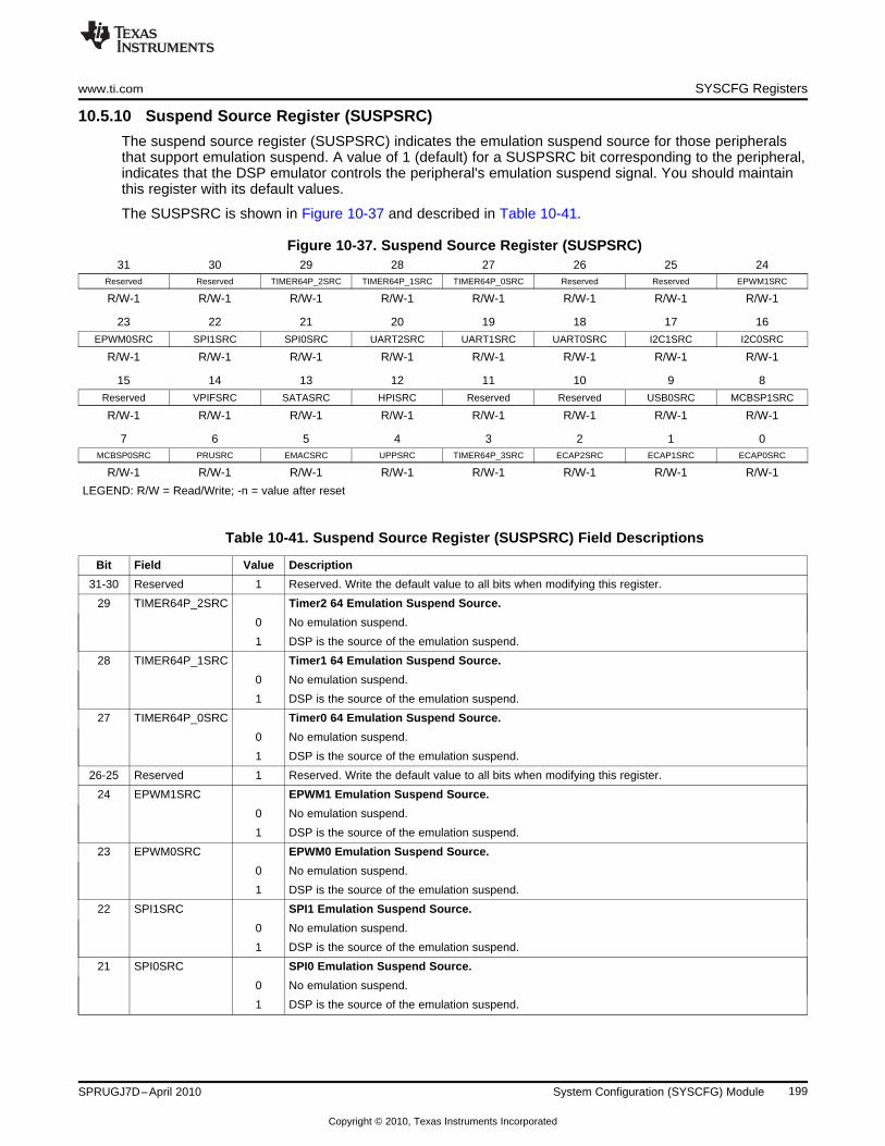
www.ti.com SYSCFG Registers
10.5.10 Suspend Source Register (SUSPSRC)
The suspend source register (SUSPSRC) indicates the emulation suspend source for those peripheralsthat support emulation suspend. A value of 1 (default) for a SUSPSRC bit corresponding to the peripheral,indicates that the DSP emulator controls the peripheral's emulation suspend signal. You should maintainthis register with its default values.
The SUSPSRC is shown in Figure 10-37 and described in Table 10-41.
Figure 10-37. Suspend Source Register (SUSPSRC)31 30 29 28 27 26 25 24
Reserved Reserved TIMER64P_2SRC TIMER64P_1SRC TIMER64P_0SRC Reserved Reserved EPWM1SRC
R/W-1 R/W-1 R/W-1 R/W-1 R/W-1 R/W-1 R/W-1 R/W-1
23 22 21 20 19 18 17 16
EPWM0SRC SPI1SRC SPI0SRC UART2SRC UART1SRC UART0SRC I2C1SRC I2C0SRC
R/W-1 R/W-1 R/W-1 R/W-1 R/W-1 R/W-1 R/W-1 R/W-1
15 14 13 12 11 10 9 8
Reserved VPIFSRC SATASRC HPISRC Reserved Reserved USB0SRC MCBSP1SRC
R/W-1 R/W-1 R/W-1 R/W-1 R/W-1 R/W-1 R/W-1 R/W-1
7 6 5 4 3 2 1 0MCBSP0SRC PRUSRC EMACSRC UPPSRC TIMER64P_3SRC ECAP2SRC ECAP1SRC ECAP0SRC
R/W-1 R/W-1 R/W-1 R/W-1 R/W-1 R/W-1 R/W-1 R/W-1
LEGEND: R/W = Read/Write; -n = value after reset
Table 10-41. Suspend Source Register (SUSPSRC) Field Descriptions
Bit Field Value Description
31-30 Reserved 1 Reserved. Write the default value to all bits when modifying this register.
29 TIMER64P_2SRC Timer2 64 Emulation Suspend Source.
0 No emulation suspend.
1 DSP is the source of the emulation suspend.
28 TIMER64P_1SRC Timer1 64 Emulation Suspend Source.
0 No emulation suspend.
1 DSP is the source of the emulation suspend.
27 TIMER64P_0SRC Timer0 64 Emulation Suspend Source.
0 No emulation suspend.
1 DSP is the source of the emulation suspend.
26-25 Reserved 1 Reserved. Write the default value to all bits when modifying this register.
24 EPWM1SRC EPWM1 Emulation Suspend Source.
0 No emulation suspend.
1 DSP is the source of the emulation suspend.
23 EPWM0SRC EPWM0 Emulation Suspend Source.
0 No emulation suspend.
1 DSP is the source of the emulation suspend.
22 SPI1SRC SPI1 Emulation Suspend Source.
0 No emulation suspend.
1 DSP is the source of the emulation suspend.
21 SPI0SRC SPI0 Emulation Suspend Source.
0 No emulation suspend.
1 DSP is the source of the emulation suspend.
199SPRUGJ7D–April 2010 System Configuration (SYSCFG) Module
Copyright © 2010, Texas Instruments Incorporated

SYSCFG Registers www.ti.com
Table 10-41. Suspend Source Register (SUSPSRC) Field Descriptions (continued)
Bit Field Value Description
20 UART2SRC UART2 Emulation Suspend Source.
0 No emulation suspend.
1 DSP is the source of the emulation suspend.
19 UART1SRC UART1 Emulation Suspend Source.
0 No emulation suspend.
1 DSP is the source of the emulation suspend.
18 UART0SRC UART0 Emulation Suspend Source.
0 No emulation suspend.
1 DSP is the source of the emulation suspend.
17 I2C1SRC I2C1 Emulation Suspend Source.
0 No emulation suspend.
1 DSP is the source of the emulation suspend.
16 I2C0SRC I2C0 Emulation Suspend Source.
0 No emulation suspend.
1 DSP is the source of the emulation suspend.
15 Reserved 1 Reserved. Write the default value to all bits when modifying this register.
14 VPIFSRC VPIF Emulation Suspend Source.
0 No emulation suspend.
1 DSP is the source of the emulation suspend.
13 SATASRC SATA Emulation Suspend Source.
0 No emulation suspend.
1 DSP is the source of the emulation suspend.
12 HPISRC HPI Emulation Suspend Source.
0 No emulation suspend.
1 DSP is the source of the emulation suspend.
11-10 Reserved 1 Reserved. Write the default value to all bits when modifying this register.
9 USB0SRC USB0 (USB 2.0) Emulation Suspend Source.
0 No emulation suspend.
1 DSP is the source of the emulation suspend.
8 MCBSP1SRC McBSP1 Emulation Suspend Source.
0 No emulation suspend.
1 DSP is the source of the emulation suspend.
7 MCBSP0SRC McBSP0 Emulation Suspend Source.
0 No emulation suspend.
1 DSP is the source of the emulation suspend.
6 PRUSRC PRU Emulation Suspend Source.
0 No emulation suspend.
1 DSP is the source of the emulation suspend.
5 EMACSRC EMAC Emulation Suspend Source.
0 No emulation suspend.
1 DSP is the source of the emulation suspend.
4 UPPSRC uPP Emulation Suspend Source.
0 No emulation suspend.
1 DSP is the source of the emulation suspend.
3 TIMER64P_3SRC Timer3 64 Emulation Suspend Source.
0 No emulation suspend.
1 DSP is the source of the emulation suspend.
200 System Configuration (SYSCFG) Module SPRUGJ7D–April 2010
Copyright © 2010, Texas Instruments Incorporated

www.ti.com SYSCFG Registers
Table 10-41. Suspend Source Register (SUSPSRC) Field Descriptions (continued)
Bit Field Value Description
2 ECAP2SRC ECAP2 Emulation Suspend Source.
0 No emulation suspend.
1 DSP is the source of the emulation suspend.
1 ECAP1SRC ECAP1 Emulation Suspend Source.
0 No emulation suspend.
1 DSP is the source of the emulation suspend.
0 ECAP0SRC ECAP0 Emulation Suspend Source.
0 No emulation suspend.
1 DSP is the source of the emulation suspend.
201SPRUGJ7D–April 2010 System Configuration (SYSCFG) Module
Copyright © 2010, Texas Instruments Incorporated
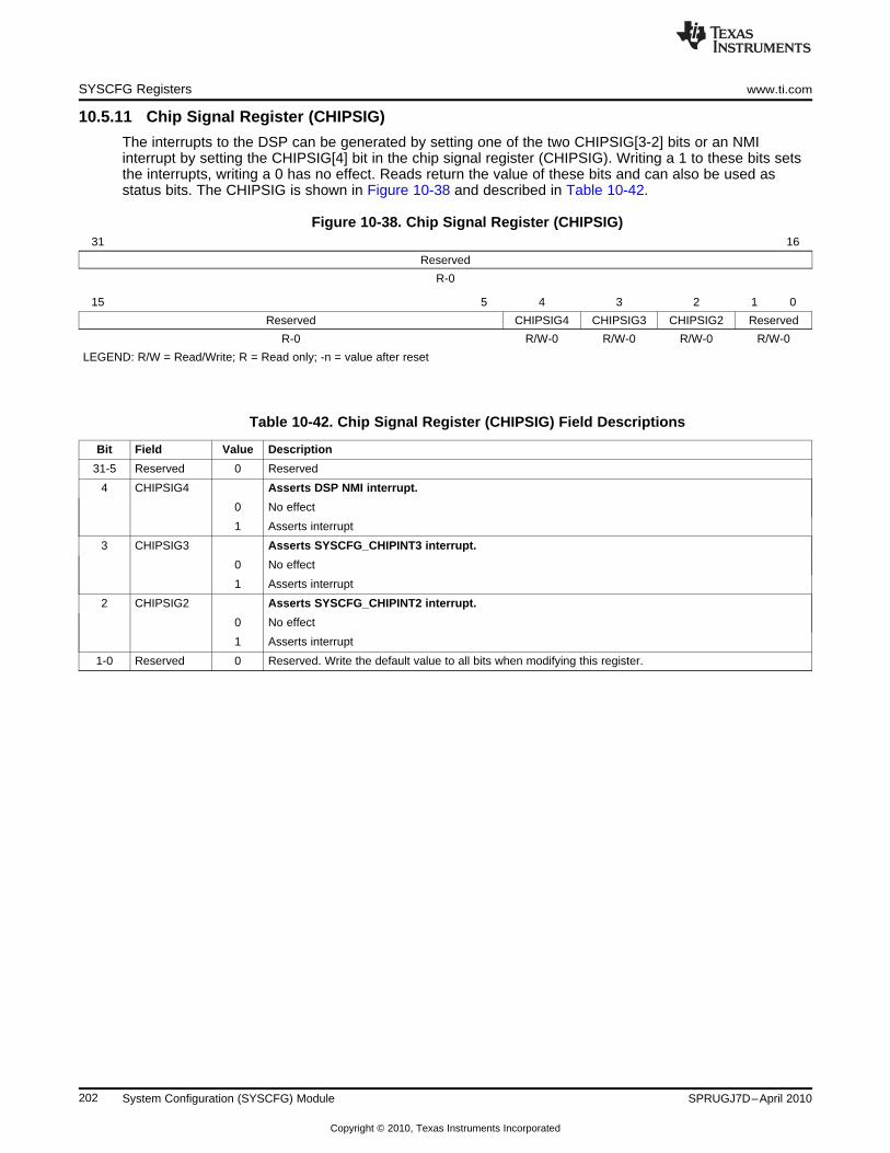
SYSCFG Registers www.ti.com
10.5.11 Chip Signal Register (CHIPSIG)
The interrupts to the DSP can be generated by setting one of the two CHIPSIG[3-2] bits or an NMIinterrupt by setting the CHIPSIG[4] bit in the chip signal register (CHIPSIG). Writing a 1 to these bits setsthe interrupts, writing a 0 has no effect. Reads return the value of these bits and can also be used asstatus bits. The CHIPSIG is shown in Figure 10-38 and described in Table 10-42.
Figure 10-38. Chip Signal Register (CHIPSIG)31 16
Reserved
R-0
15 5 4 3 2 1 0
Reserved CHIPSIG4 CHIPSIG3 CHIPSIG2 Reserved
R-0 R/W-0 R/W-0 R/W-0 R/W-0
LEGEND: R/W = Read/Write; R = Read only; -n = value after reset
Table 10-42. Chip Signal Register (CHIPSIG) Field Descriptions
Bit Field Value Description
31-5 Reserved 0 Reserved
4 CHIPSIG4 Asserts DSP NMI interrupt.
0 No effect
1 Asserts interrupt
3 CHIPSIG3 Asserts SYSCFG_CHIPINT3 interrupt.
0 No effect
1 Asserts interrupt
2 CHIPSIG2 Asserts SYSCFG_CHIPINT2 interrupt.
0 No effect
1 Asserts interrupt
1-0 Reserved 0 Reserved. Write the default value to all bits when modifying this register.
202 System Configuration (SYSCFG) Module SPRUGJ7D–April 2010
Copyright © 2010, Texas Instruments Incorporated

www.ti.com SYSCFG Registers
10.5.12 Chip Signal Clear Register (CHIPSIG_CLR)
The chip signal clear register (CHIPSIG_CLR) is used to clear the bits set in the chip signal register(CHIPSIG). Writing a 1 to a CHIPSIG[n] bit in CHIPSIG_CLR clears the corresponding CHIPSIG[n] bit inCHIPSIG; writing a 0 has no effect. After servicing the interrupt, the interrupted processor can clear thebits set in CHIPSIG by writing 1 to the corresponding bits in CHIPSIG_CLR. The other processor may pollthe CHIPSIG[n] bit to determine when the interrupted processor has completed the interrupt service. TheCHIPSIG_CLR is shown in Figure 10-39 and described in Table 10-43.
For more information on DSP interrupts, see Chapter 2.
Figure 10-39. Chip Signal Clear Register (CHIPSIG_CLR)31 16
Reserved
R-0
15 5 4 3 2 1 0
Reserved CHIPSIG4 CHIPSIG3 CHIPSIG2 Reserved
R-0 R/W-0 R/W-0 R/W-0 R/W-0
LEGEND: R/W = Read/Write; R = Read only; -n = value after reset
Table 10-43. Chip Signal Clear Register (CHIPSIG_CLR) Field Descriptions
Bit Field Value Description
31-5 Reserved 0 Reserved
4 CHIPSIG4 Clears DSP NMI interrupt.
0 No effect
1 Clears interrupt
3 CHIPSIG3 Clears SYSCFG_CHIPINT3 interrupt.
0 No effect
1 Clears interrupt
2 CHIPSIG2 Clears SYSCFG_CHIPINT2 interrupt.
0 No effect
1 Clears interrupt
1-0 Reserved 0 Reserved. Write the default value to all bits when modifying this register.
203SPRUGJ7D–April 2010 System Configuration (SYSCFG) Module
Copyright © 2010, Texas Instruments Incorporated

SYSCFG Registers www.ti.com
10.5.13 Chip Configuration 0 Register (CFGCHIP0)
The chip configuration 0 register (CFGCHIP0) controls the following functions:
• PLL Controller 0 memory-mapped register lock: Used to lock out writes to the PLLC0 memory-mappedregisters (MMRs) to prevent any erroneous writes in software to the PLLC0 register space.
• EDMA3_0 Transfer Controller Default Burst Size (DBS) Control: This controls the maximum number ofbytes issued per read/write command or the burst size for the individual transfer controllers (TCs) onthe device. By default for all transfer controllers, the burst size is set to 16 bytes. However, CFGCHIP0allows configurability of this parameter so that the TC can have a burst size of 16, 32, or 64 bytes. Theburst size determines the intra packet efficiency for the EDMA3_0 transfers. Additionally, it alsofacilitates preemption at a system level, as all transfer requests are internally broken down by thetransfer controller up to DBS size byte chunks and on a system level, each master’s priority(configured by the MSTPRI register) is evaluated at burst size boundaries. The DBS value cansignificantly impact the standalone throughput performance depending on the source and destination(bus width/frequency/burst support etc) and the TC FIFO size, etc. Therefore, the DBS sizeconfiguration should be carefully analyzed to meet the system’s throughput/performance requirements.
The CFGCHIP0 is shown in Figure 10-40 and described in Table 10-44.
Figure 10-40. Chip Configuration 0 Register (CFGCHIP0)31 16
Reserved
R-0
15 5 4 3 2 1 0
Reserved PLL_MASTER_LOCK EDMA30TC1DBS EDMA30TC0DBS
R-0 R/W-0 R/W-0 R/W-0
LEGEND: R/W = Read/Write; R = Read only; -n = value after reset
Table 10-44. Chip Configuration 0 Register (CFGCHIP0) Field Descriptions
Bit Field Value Description
31-5 Reserved 0 Reserved.
4 PLL_MASTER_LOCK PLLC0 MMRs lock.
0 PLLC0 MMRs are freely accessible.
1 All PLLC0 MMRs are locked.
3-2 EDMA30TC1DBS EDMA3_0_TC1 Default Burst Size (DBS).
0 16 bytes
1h 32 bytes
2h 64 bytes
3h Reserved
1-0 EDMA30TC0DBS EDMA3_0_TC0 Default Burst Size (DBS).
0 16 bytes
1h 32 bytes
2h 64 bytes
3h Reserved
204 System Configuration (SYSCFG) Module SPRUGJ7D–April 2010
Copyright © 2010, Texas Instruments Incorporated

www.ti.com SYSCFG Registers
10.5.14 Chip Configuration 1 Register (CFGCHIP1)
The chip configuration 1 register (CFGCHIP1) controls the following functions:
• eCAP0/1/2 event input source: Allows using McASP0 TX/RX events or various EMAC TX/RXthreshold, pulse, or miscellaneous interrupt events as eCAP event input sources.
• HPI Control: Allows HPIEN bit control that determines whether or not the HPI module has control overthe HPI pins (multiplexed with other peripheral pins). It also provides configurability to select whetherthe host address is a word address or a byte address mode.
• EDMA3_1 Transfer Controller Default Burst Size (DBS) Control: This controls the maximum number ofbytes issued per read/write command or the burst size for the individual transfer controllers (TCs) onthe device. By default for all transfer controllers, the burst size is set to 16 bytes. However, CFGCHIP1allows configurability of this parameter so that the TC can have a burst size of 16, 32, or 64 bytes. Theburst size determines the intra packet efficiency for the EDMA3_1 transfers. Additionally, it alsofacilitates preemption at a system level, as all transfer requests are internally broken down by thetransfer controller up to DBS size byte chunks and on a system level, each master’s priority(configured by the MSTPRI register) is evaluated at burst size boundaries. The DBS value cansignificantly impact the standalone throughput performance depending on the source and destination(bus width/frequency/burst support etc) and the TC FIFO size, etc. Therefore, the DBS sizeconfiguration should be carefully analyzed to meet the system’s throughput/performance requirements.
• eHRPWM Time Base Clock (TBCLK) Synchronization: Allows the software to globally synchronize allenabled eHRPWM modules to the time base clock (TBCLK).
• McASP0 AMUTEIN signal source control: Allows selecting GPIO interrupt from different banks assource for the McASP0 AMUTEIN signal.
The CFGCHIP1 is shown in Figure 10-41 and described in Table 10-45.
Figure 10-41. Chip Configuration 1 Register (CFGCHIP1)31 27 26 22 21 17 16
CAP2SRC CAP1SRC CAP0SRC HPIBYTEAD
R/W-0 R/W-0 R/W-0 R/W-0
15 14 13 12 11 8
HPIENA EDMA31TC0DBS TBCLKSYNC Reserved
R/W-0 R-0 R/W-0 R/W-0
7 4 3 0
Reserved AMUTESEL0
R/W-0 R/W-0
LEGEND: R/W = Read/Write; R = Read only; -n = value after reset
205SPRUGJ7D–April 2010 System Configuration (SYSCFG) Module
Copyright © 2010, Texas Instruments Incorporated

SYSCFG Registers www.ti.com
Table 10-45. Chip Configuration 1 Register (CFGCHIP1) Field Descriptions
Bit Field Value Description
31-27 CAP2SRC Selects the eCAP2 module event input.
0 eCAP2 Pin input
1h McASP0 TX DMA Event
2h McASP0 RX DMA Event
3h-6h Reserved
7h EMAC C0 RX Threshold Pulse Interrupt
8h EMAC C0 RX Pulse Interrupt
9h EMAC C0 TX Pulse Interrupt
Ah EMAC C0 Miscellaneous Interrupt
Bh EMAC C1 RX Threshold Pulse Interrupt
Ch EMAC C1 RX Pulse Interrupt
Dh EMAC C1 TX Pulse Interrupt
Eh EMAC C1 Miscellaneous Interrupt
Fh EMAC C2 RX Threshold Pulse Interrupt
10h EMAC C2 RX Pulse Interrupt
11h EMAC C2 TX Pulse Interrupt
12h EMAC C2 Miscellaneous Interrupt
13h-1Fh Reserved
26-22 CAP1SRC Selects the eCAP1 module event input.
0 eCAP1 Pin input
1h McASP0 TX DMA Event
2h McASP0 RX DMA Event
3h-6h Reserved
7h EMAC C0 RX Threshold Pulse Interrupt
8h EMAC C0 RX Pulse Interrupt
9h EMAC C0 TX Pulse Interrupt
Ah EMAC C0 Miscellaneous Interrupt
Bh EMAC C1 RX Threshold Pulse Interrupt
Ch EMAC C1 RX Pulse Interrupt
Dh EMAC C1 TX Pulse Interrupt
Eh EMAC C1 Miscellaneous Interrupt
Fh EMAC C2 RX Threshold Pulse Interrupt
10h EMAC C2 RX Pulse Interrupt
11h EMAC C2 TX Pulse Interrupt
12h EMAC C2 Miscellaneous Interrupt
13h-1Fh Reserved
206 System Configuration (SYSCFG) Module SPRUGJ7D–April 2010
Copyright © 2010, Texas Instruments Incorporated

www.ti.com SYSCFG Registers
Table 10-45. Chip Configuration 1 Register (CFGCHIP1) Field Descriptions (continued)
Bit Field Value Description
21-17 CAP0SRC Selects the eCAP0 module event input.
0 eCAP0 Pin input
1h McASP0 TX DMA Event
2h McASP0 RX DMA Event
3h-6h Reserved
7h EMAC C0 RX Threshold Pulse Interrupt
8h EMAC C0 RX Pulse Interrupt
9h EMAC C0 TX Pulse Interrupt
Ah EMAC C0 Miscellaneous Interrupt
Bh EMAC C1 RX Threshold Pulse Interrupt
Ch EMAC C1 RX Pulse Interrupt
Dh EMAC C1 TX Pulse Interrupt
Eh EMAC C1 Miscellaneous Interrupt
Fh EMAC C2 RX Threshold Pulse Interrupt
10h EMAC C2 RX Pulse Interrupt
11h EMAC C2 TX Pulse Interrupt
12h EMAC C2 Miscellaneous Interrupt
13h-1Fh Reserved
16 HPIBYTEAD HPI Byte/Word Address Mode select.
0 Host address is a word address.
1 Host address is a byte address.
15 HPIENA HPI Enable Bit.
0 HPI is disabled.
1 HPI is enabled.
14-13 EDMA31TC0DBS EDMA3_1_TC0 Default Burst Size.
0 16 bytes
1h 32 bytes
2h 64 bytes
3h Reserved
12 TBCLKSYNC eHRPWM Module Time Base Clock Synchronization. Allows you to globally synchronize allenabled eHRPWM modules to the time base clock (TBCLK).
0 Time base clock (TBCLK) within each enabled eHRPWM module is stopped.
1 All enabled eHRPWM module clocks are started with the first rising edge of TBCLK aligned. Forperfectly synchronized TBCLKs, the prescaler bits in the TBCTL register of each eHRPWMmodule must be set identically.
11-4 Reserved 0 Reserved. Write the default value to all bits when modifying this register.
3-0 AMUTESEL0 Selects the source of McASP0 AMUTEIN signal.
0 Drive McASP0 AMUTEIN signal low.
1h GPIO Interrupt from Bank 0
2h GPIO Interrupt from Bank 1
3h GPIO Interrupt from Bank 2
4h GPIO Interrupt from Bank 3
5h GPIO Interrupt from Bank 4
6h GPIO Interrupt from Bank 5
7h GPIO Interrupt from Bank 6
8h GPIO Interrupt from Bank 7
9h-Fh Reserved
207SPRUGJ7D–April 2010 System Configuration (SYSCFG) Module
Copyright © 2010, Texas Instruments Incorporated

SYSCFG Registers www.ti.com
10.5.15 Chip Configuration 2 Register (CFGCHIP2)
The chip configuration 2 register (CFGCHIP2) controls the following functions:
• USB1.1 OHCI• USB2.0 OTG PHY
The CFGCHIP2 is shown in Figure 10-42 and described in Table 10-46.
Figure 10-42. Chip Configuration 2 Register (CFGCHIP2)31 24
Reserved
R-0
23 18 17 16Reserved USB0PHYCLKGD USB0VBUSSENSE
R-0 R-0 R-0
15 14 13 12 11 10 9 8RESET USB0OTGMODE USB1PHYCLKMUX USB0PHYCLKMUX USB0PHYPWDN USB0OTGPWRDN USB0DATPOL
R/W-1 R/W-3h R/W-0 R/W-1 R/W-1 R/W-1 R/W-1
7 6 5 4 3 0USB1SUSPENDM USB0PHY_PLLON USB0SESNDEN USB0VBDTCTEN USB0REF_FREQ
R/W-0 R/W-0 R/W-0 R/W-0 R/W-0
LEGEND: R/W = Read/Write; R = Read only; -n = value after reset
Table 10-46. Chip Configuration 2 Register (CFGCHIP2) Field Descriptions
Bit Field Value Description
31-18 Reserved 0 Reserved
17 USB0PHYCLKGD Status of USB2.0 PHY.
0 Clock is not present, power is not good, and PLL has not locked.
1 Clock is present, power is good, and PLL has locked.
16 USB0VBUSSENSE Status of USB2.0 PHY VBUS sense.
0 PHY is not sensing voltage presence on the VBUS pin.
1 PHY is sensing voltage presence on the VBUS pin.
15 RESET USB2.0 PHY reset.
0 Not in reset.
1 USB2.0 PHY in reset.
14-13 USB0OTGMODE USB2.0 OTG subsystem mode.
0 No override. PHY drive signals to controller based on its comparators for VBUS and ID pins.
1h Override phy values to force USB host operation.
2h Override phy values to force USB device operation.
3h Override phy values to force USB host operation with VBUS low.
12 USB1PHYCLKMUX USB1.1 PHY reference clock input mux. Controls clock mux to USB1.1.
0 USB1.1 PHY reference clock is sourced by output of USB2.0 PHY.
1 USB1.1 PHY reference clock (USB_REFCLKIN) is sourced by an external pin.
11 USB0PHYCLKMUX USB2.0 PHY reference clock input mux.
0 USB2.0 PHY reference clock (USB_REFCLKIN) is sourced by an external pin.
1 USB2.0 PHY reference clock (AUXCLK) is internally generated from the PLL.
10 USB0PHYPWDN USB2.0 PHY operation state control.
0 USB2.0 PHY is enabled and is in operating state (normal operation).
1 USB2.0 PHY is disabled and powered down.
208 System Configuration (SYSCFG) Module SPRUGJ7D–April 2010
Copyright © 2010, Texas Instruments Incorporated

www.ti.com SYSCFG Registers
Table 10-46. Chip Configuration 2 Register (CFGCHIP2) Field Descriptions (continued)
Bit Field Value Description
9 USB0OTGPWRDN USB2.0 OTG subsystem (SS) operation state control.
0 OTG SS is enabled and is in operating state (normal operation).
1 OTG SS is disabled and is powered down.
8 USB0DATPOL USB2.0 differential data lines polarity selector.
0 Differential data polarities are inverted (USB_DP is connected to D- and USB_DM isconnected to D+).
1 Differential data polarity are not altered (USB_DP is connected to D+ and USB_DM isconnected to D-).
7 USB1SUSPENDM USB1.1 suspend mode.
0 Needs to be 0 whenever USB1.1 PHY is unpowered.
1 Enable USB1.1 PHY.
6 USB0PHY_PLLON Drives USB2.0 PHY, allowing or preventing it from stopping the 48 MHz clock duringUSB SUSPEND.
0 USB2.0 PHY is allowed to stop the 48 MHz clock during USB SUSPEND.
1 USB2.0 PHY is prevented from stopping the 48 MHz clock during USB SUSPEND
5 USB0SESNDEN USB2.0 Session End comparator enable.
0 Session End comparator is disabled.
1 Session End comparator is enabled.
4 USB0VBDTCTEN USB2.0 VBUS line comparators enable.
0 All VBUS line comparators are disabled.
1 All VBUS line comparators are enabled.
3-0 USB0REF_FREQ USB2.0 PHY reference clock input frequencies.
0 Reserved
1h 12 MHz
2h 24 MHz
3h 48 MHz
4h 19.2 MHz
5h 38.4 MHz
6h 13 MHz
7h 26 MHz
8h 20 MHz
9h 40 MHz
Ah-Fh Reserved
209SPRUGJ7D–April 2010 System Configuration (SYSCFG) Module
Copyright © 2010, Texas Instruments Incorporated

SYSCFG Registers www.ti.com
10.5.16 Chip Configuration 3 Register (CFGCHIP3)
The chip configuration 3 register (CFGCHIP3) controls the following peripheral/module functions:
• EMAC MII/RMII Mode Select.• uPP Clock Source Control: Allows control for the source of the uPP 2x transmit clock.• PLL Controller 1 memory-mapped register lock: Used to lock out writes to the PLLC1 memory-mapped
registers (MMRs) to prevent any erroneous writes in software to the PLLC1 register space.• ASYNC3 Clock Source Control: Allows control for the source of the ASYNC3 clock.• PRU Event Input Select.• DIV4p5 Clock Enable/Disable: The DIV4p5 (/4.5) hardware clock divider is provided to generate
133 MHz from the 600 MHz PLL clock for use as clocks to the EMIFs. Allows enabling/disabling thisclock divider.
• EMIFA Module Clock Source Control: Allows control for the source of the EMIFA module clock.
The CFGCHIP3 is shown in Figure 10-43 and described in Table 10-47.
Figure 10-43. Chip Configuration 3 Register (CFGCHIP3)31 16
Reserved
R-0
15 9 8
Reserved RMII_SEL
R/W-7Fh R/W-1
7 6 5 4 3 2 1 0Reserved UPP_TX_CLKSRC PLL1_MASTER_LOCK ASYNC3_CLKSRC PRUEVTSEL DIV45PENA EMA_CLKSRC Reserved
R/W-0 R/W-0 R/W-0 R/W-0 R/W-0 R/W-0 R/W-0 R/W-0
LEGEND: R/W = Read/Write; R = Read only; -n = value after reset
Table 10-47. Chip Configuration 3 Register (CFGCHIP3) Field Descriptions
Bit Field Value Description
31-16 Reserved 0 Reserved
15-9 Reserved 7Fh Reserved. Write the default value to all bits when modifying this register.
8 RMII_SEL EMAC MII/RMII mode select.
0 MII mode
1 RMII mode
7 Reserved 0 Reserved. Write the default value when modifying this register.
6 UPP_TX_CLKSRC Clock source for uPP 2x transmit clock.
0 Clock driven by ASYNC3.
1 Clock driven by external signal, 2xTXCLK.
5 PLL1_MASTER_LOCK PLLC1 MMRs lock.
0 PLLC1 MMRs are freely accessible.
1 All PLLC1 MMRs are locked.
4 ASYNC3_CLKSRC Clock source for ASYNC3.
0 Clock driven by PLL0_SYSCLK2.
1 Clock driven by PLL1_SYSCLK2.
3 PRUEVTSEL PRU event input select.
0 Normal mode
1 Alternate mode
210 System Configuration (SYSCFG) Module SPRUGJ7D–April 2010
Copyright © 2010, Texas Instruments Incorporated

www.ti.com SYSCFG Registers
Table 10-47. Chip Configuration 3 Register (CFGCHIP3) Field Descriptions (continued)
Bit Field Value Description
2 DIV45PENA Controls the fixed DIV4.5 divider in the PLL controller.
0 Divide by 4.5 is disabled.
1 Divide by 4.5 is enabled.
1 EMA_CLKSRC Clock source for EMIFA clock domain.
0 Clock driven by PLL0_SYSCLK3
1 Clock driven by DIV4.5 PLL output
0 Reserved 0 Reserved. Write the default value when modifying this register.
10.5.17 Chip Configuration 4 Register (CFGCHIP4)
The chip configuration 4 register (CFGCHIP4) is used for clearing the AMUNTEIN signal for McASP0.Writing a 1 causes a single pulse that clears the latched GPIO interrupt for AMUTEIN of McASP0, if it waspreviously set; reads always return a value of 0. The CFGCHIP4 is shown in Figure 10-44 and describedin Table 10-48.
Figure 10-44. Chip Configuration 4 Register (CFGCHIP4)31 16
Reserved
R-0
15 8 7 1 0
Reserved Reserved AMUTECLR0
R/W-FFh R/W-0 R/W-0
LEGEND: R/W = Read/Write; R = Read only; -n = value after reset
Table 10-48. Chip Configuration 4 Register (CFGCHIP4) Field Descriptions
Bit Field Value Description
31-16 Reserved 0 Reserved
15-8 Reserved FFh Reserved. Write the default value to all bits when modifying this register.
7-1 Reserved 0 Reserved. Write the default value to all bits when modifying this register.
0 AMUTECLR0 Clears the latched GPIO interrupt for AMUTEIN of McASP0 when set to 1.
0 No effect
1 Clears interrupt
211SPRUGJ7D–April 2010 System Configuration (SYSCFG) Module
Copyright © 2010, Texas Instruments Incorporated

SYSCFG Registers www.ti.com
10.5.18 VTP I/O Control Register (VTPIO_CTL)
The VTP I/O control register (VTPIO_CTL) is used to control the calibration of the DDR2/mDDR memorycontroller I/Os with respect to voltage, temperature, and process (VTP). The voltage, temperature, andprocess information is used to control the IO's output impedance. The VTPIO_CTL is shown inFigure 10-45 and described in Table 10-49.
Figure 10-45. VTP I/O Control Register (VTPIO_CTL)31 24
Reserved
R-0
23 19 18 17 16
Reserved VREFEN VREFTAP
R-0 R/W-0 R/W-0
15 14 13 12 11 10 9 8
READY IOPWRDN CLKRZ FORCEDNP FORCEDNN FORCEUPP FORCEUPN PWRSAVE
R-0 R/W-0 R/W-0 R/W-0 R/W-0 R/W-0 R/W-0 R/W-0
7 6 5 4 3 2 1 0
LOCK POWERDN D0 D1 D2 F0 F1 F2
R/W-0 R/W-1 R/W-1 R/W-1 R/W-0 R/W-1 R/W-1 R/W-1
LEGEND: R/W = Read/Write; R = Read only; -n = value after reset
Table 10-49. VTP I/O Control Register (VTPIO_CTL) Field Descriptions
Bit Field Value Description
31-19 Reserved 0 Reserved
18 VREFEN Internal DDR I/O Vref enable.
0 Connected to pad, external reference.
1 Connected to internal reference.
17-16 VREFTAP Selection for internal reference voltage level.
0 Vref = 50.0% of VDDS
1h Vref = 47.5% of VDDS
2h Vref = 52.5% of VDDS
3h Reserved
15 READY VTP Ready status.
0 VTP is not ready.
1 VTP is ready.
14 IOPWRDN Power down enable for DDR input buffer.
0 Disable power down control by the PWRDNEN bit in the DDR PHY control register 1 (DRPYC1R).
1 Enable power down control by the PWRDNEN bit in the DDR PHY control register 1 (DRPYC1R).
13 CLKRZ 0 VTP clear. Write 0 to clear VTP flops.
12 FORCEDNP 0 Force decrease PFET drive.
11 FORCEDNN 0 Force decrease NFET drive.
10 FORCEUPP 0 Force increase PFET drive.
9 FORCEUPN 0 Force increase PFET drive.
8 PWRSAVE VTP power save mode.
0 Disable power save mode.
1 Enable power save mode.
7 LOCK VTP impedance lock.
0 Unlock impedance.
1 Lock impedance.
212 System Configuration (SYSCFG) Module SPRUGJ7D–April 2010
Copyright © 2010, Texas Instruments Incorporated

www.ti.com SYSCFG Registers
Table 10-49. VTP I/O Control Register (VTPIO_CTL) Field Descriptions (continued)
Bit Field Value Description
6 POWERDN VTP power down.
0 Disable power down.
1 Enable power down.
5 D0 1 Drive strength control bit.
4 D1 1 Drive strength control bit.
3 D2 0 Drive strength control bit.
2 F0 1 Digital filter control bit.
1 F1 1 Digital filter control bit.
0 F2 1 Digital filter control bit.
213SPRUGJ7D–April 2010 System Configuration (SYSCFG) Module
Copyright © 2010, Texas Instruments Incorporated
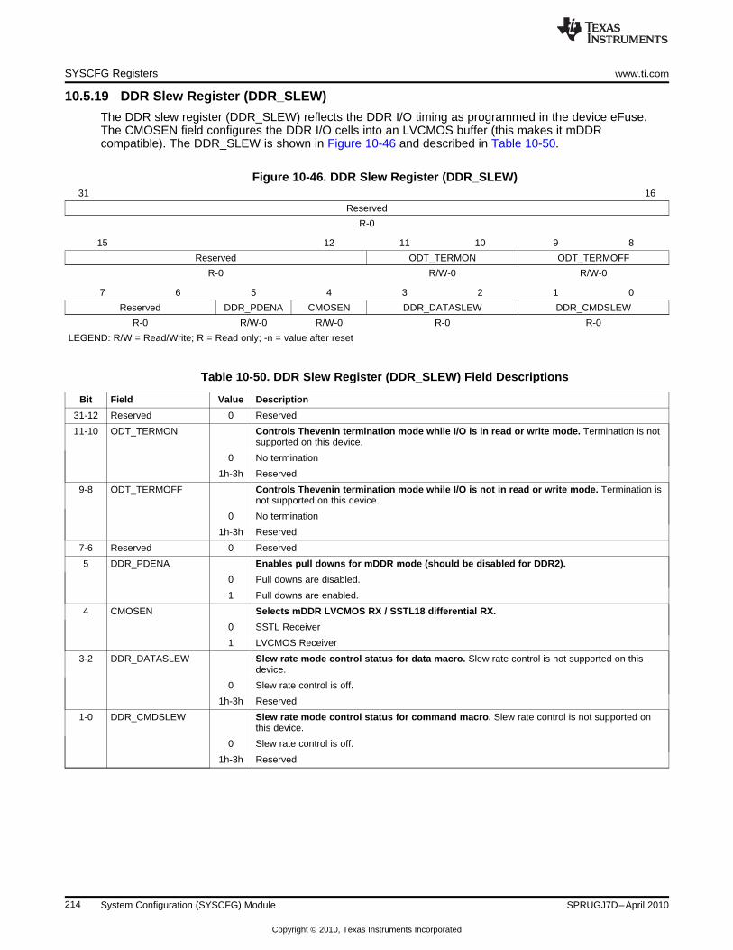
SYSCFG Registers www.ti.com
10.5.19 DDR Slew Register (DDR_SLEW)
The DDR slew register (DDR_SLEW) reflects the DDR I/O timing as programmed in the device eFuse.The CMOSEN field configures the DDR I/O cells into an LVCMOS buffer (this makes it mDDRcompatible). The DDR_SLEW is shown in Figure 10-46 and described in Table 10-50.
Figure 10-46. DDR Slew Register (DDR_SLEW)31 16
Reserved
R-0
15 12 11 10 9 8
Reserved ODT_TERMON ODT_TERMOFF
R-0 R/W-0 R/W-0
7 6 5 4 3 2 1 0
Reserved DDR_PDENA CMOSEN DDR_DATASLEW DDR_CMDSLEW
R-0 R/W-0 R/W-0 R-0 R-0
LEGEND: R/W = Read/Write; R = Read only; -n = value after reset
Table 10-50. DDR Slew Register (DDR_SLEW) Field Descriptions
Bit Field Value Description
31-12 Reserved 0 Reserved
11-10 ODT_TERMON Controls Thevenin termination mode while I/O is in read or write mode. Termination is notsupported on this device.
0 No termination
1h-3h Reserved
9-8 ODT_TERMOFF Controls Thevenin termination mode while I/O is not in read or write mode. Termination isnot supported on this device.
0 No termination
1h-3h Reserved
7-6 Reserved 0 Reserved
5 DDR_PDENA Enables pull downs for mDDR mode (should be disabled for DDR2).
0 Pull downs are disabled.
1 Pull downs are enabled.
4 CMOSEN Selects mDDR LVCMOS RX / SSTL18 differential RX.
0 SSTL Receiver
1 LVCMOS Receiver
3-2 DDR_DATASLEW Slew rate mode control status for data macro. Slew rate control is not supported on thisdevice.
0 Slew rate control is off.
1h-3h Reserved
1-0 DDR_CMDSLEW Slew rate mode control status for command macro. Slew rate control is not supported onthis device.
0 Slew rate control is off.
1h-3h Reserved
214 System Configuration (SYSCFG) Module SPRUGJ7D–April 2010
Copyright © 2010, Texas Instruments Incorporated

www.ti.com SYSCFG Registers
10.5.20 Deep Sleep Register (DEEPSLEEP)
The deep sleep register (DEEPSLEEP) control the Deep Sleep logic. See the device-specific data manualand Chapter 11 for details on boot and configuration settings. The DEEPSLEEP is shown in Figure 10-47and described in Table 10-51.
Figure 10-47. Deep Sleep Register (DEEPSLEEP)31 30 29 16
SLEEPENABLE SLEEPCOMPLETE Reserved
R/W-0 R-0 R-0
15 0
SLEEPCOUNT
R/W-FFFFh
LEGEND: R/W = Read/Write; R = Read only; -n = value after reset
Table 10-51. Deep Sleep Register (DEEPSLEEP) Field Descriptions
Bit Field Value Description
31 SLEEPENABLE Deep sleep enable. The software must clear this bit to 0 when the device is awakened fromdeep sleep.
0 Device is in normal operating mode; DEEPSLEEP pin has no effect.
1 Deep sleep mode is enabled; setting DEEPSLEEP pin low initiates oscillator shut down.
30 SLEEPCOMPLETE Deep sleep complete. Once the deep sleep process starts, the software must poll theSLEEPCOMPLETE bit; when the SLEEPCOMPLETE bit is read as 1, the software shouldclear the SLEEPENABLE bit and continue operation.
0 SLEEPCOUNT delay is not complete.
1 SLEEPCOUNT delay is complete.
29-16 Reserved 0 Reserved
15-0 SLEEPCOUNT 0-FFFFh Deep sleep counter. Number of cycles to count prior to the oscillator being stable. All 16bits are tied directly to the counter in the Deep Sleep logic.
215SPRUGJ7D–April 2010 System Configuration (SYSCFG) Module
Copyright © 2010, Texas Instruments Incorporated

SYSCFG Registers www.ti.com
10.5.21 Pullup/Pulldown Enable Register (PUPD_ENA)
The pullup/pulldown enable register (PUPD_ENA) enables the pull-up or pull-down functionality for the pingroup n defined in your device-specific data manual. The PUPD_ENA is shown in Figure 10-48 anddescribed in Table 10-52.
Figure 10-48. Pullup/Pulldown Enable Register (PUPD_ENA)31 0
PUPDENA[n]
R/W-FFFF FFFFh
LEGEND: R/W = Read/Write; -n = value after reset
Table 10-52. Pullup/Pulldown Enable Register (PUPD_ENA) Field Descriptions
Bit Field Value Description
31-0 PUPDENA[n] Enables internal pull-up or pull-down functionality for pin group CP[n]. See yourdevice-specific data manual for pin group information. The internal pull-up or pull-down functionalityselection for bit position n in PUPD_ENA is set in the same bit position n of the pullup/pulldownselect register (PUPD_SEL).
0 Internal pull-up or pull-down functionality for pin group n is disabled.
1 Internal pull-up or pull-down functionality for pin group n is enabled.
10.5.22 Pullup/Pulldown Select Register (PUPD_SEL)
The pullup/pulldown select register (PUPD_SEL) selects between the pull-up or pull-down functionality forthe pin group n defined in your device-specific data manual. The PUPD_SEL is shown in Figure 10-49 anddescribed in Table 10-53 and Table 10-54.
NOTE: The PUPD_SEL settings are not active until the device is out of reset. During reset, all ofthe CP[n] pins are weakly pulled down. If the application requires a pull-up during reset, anexternal pull-up should be used.
Figure 10-49. Pullup/Pulldown Select Register (PUPD_SEL)31 0
PUPDSEL[n]
R/W-C3FF FFFFh
LEGEND: R/W = Read/Write; -n = value after reset
Table 10-53. Pullup/Pulldown Select Register (PUPD_SEL) Field Descriptions
Bit Field Value Description
31-0 PUPDSEL[n] Selects between the internal pull-up or pull-down functionality for pin group CP[n]. See yourdevice-specific data manual for pin group information. The selection for bit position n in PUPD_SELis only valid when the same bit position n is set in the pullup/pulldown enable register(PUPD_ENA).
0 Internal pull-down functionality for pin group n is enabled.
1 Internal pull-up functionality for pin group n is enabled.
216 System Configuration (SYSCFG) Module SPRUGJ7D–April 2010
Copyright © 2010, Texas Instruments Incorporated

www.ti.com SYSCFG Registers
Table 10-54. Pullup/Pulldown Select Register (PUPD_SEL) Default Values
DefaultBit Field Value Description
31 PUPDSEL[31] 1 Pin Group CP[31] is configured for pull-up by default.
30 PUPDSEL[30] 1 Pin Group CP[30] is configured for pull-up by default.
29 PUPDSEL[29] 0 Pin Group CP[29] is configured for pull-down by default.
28 PUPDSEL[28] 0 Pin Group CP[28] is configured for pull-down by default.
27 PUPDSEL[27] 0 Pin Group CP[27] is configured for pull-down by default.
26 PUPDSEL[26] 0 Pin Group CP[26] is configured for pull-down by default.
25 PUPDSEL[25] 1 Pin Group CP[25] is configured for pull-up by default.
24 PUPDSEL[24] 1 Pin Group CP[24] is configured for pull-up by default.
23 PUPDSEL[23] 1 Pin Group CP[23] is configured for pull-up by default.
22 PUPDSEL[22] 1 Pin Group CP[22] is configured for pull-up by default.
21 PUPDSEL[21] 1 Pin Group CP[21] is configured for pull-up by default.
20 PUPDSEL[20] 1 Pin Group CP[20] is configured for pull-up by default.
19 PUPDSEL[19] 1 Pin Group CP[19] is configured for pull-up by default.
18 PUPDSEL[18] 1 Pin Group CP[18] is configured for pull-up by default.
17 PUPDSEL[17] 1 Pin Group CP[17] is configured for pull-up by default.
16 PUPDSEL[16] 1 Pin Group CP[16] is configured for pull-up by default.
15 PUPDSEL[15] 1 Pin Group CP[15] is configured for pull-up by default.
14 PUPDSEL[14] 1 Pin Group CP[14] is configured for pull-up by default.
13 PUPDSEL[13] 1 Pin Group CP[13] is configured for pull-up by default.
12 PUPDSEL[12] 1 Pin Group CP[12] is configured for pull-up by default.
11 PUPDSEL[11] 1 Pin Group CP[11] is configured for pull-up by default.
10 PUPDSEL[10] 1 Pin Group CP[10] is configured for pull-up by default.
9 PUPDSEL[9] 1 Pin Group CP[9] is configured for pull-up by default.
8 PUPDSEL[8] 1 Pin Group CP[8] is configured for pull-up by default.
7 PUPDSEL[7] 1 Pin Group CP[7] is configured for pull-up by default.
6 PUPDSEL[6] 1 Pin Group CP[6] is configured for pull-up by default.
5 PUPDSEL[5] 1 Pin Group CP[5] is configured for pull-up by default.
4 PUPDSEL[4] 1 Pin Group CP[4] is configured for pull-up by default.
3 PUPDSEL[3] 1 Pin Group CP[3] is configured for pull-up by default.
2 PUPDSEL[2] 1 Pin Group CP[2] is configured for pull-up by default.
1 PUPDSEL[1] 1 Pin Group CP[1] is configured for pull-up by default.
0 PUPDSEL[0] 1 Pin Group CP[0] is configured for pull-up by default.
217SPRUGJ7D–April 2010 System Configuration (SYSCFG) Module
Copyright © 2010, Texas Instruments Incorporated

SYSCFG Registers www.ti.com
10.5.23 RXACTIVE Control Register (RXACTIVE)
The RXACTIVE control register (RXACTIVE) enables or disables the LVCMOS receivers for the for thepin group n defined in your device-specific data manual. The RXACTIVE is shown in Figure 10-50 anddescribed in Table 10-55.
Figure 10-50. RXACTIVE Control Register (RXACTIVE)31 0
RXACTIVE[n]
R/W-FFFF FFFFh
LEGEND: R/W = Read/Write; -n = value after reset
Table 10-55. RXACTIVE Control Register (RXACTIVE) Field Descriptions
Bit Field Value Description
31-0 RXACTIVE[n] Enables the LVCMOS receivers on pin group n . See your device-specific data manual for pin groupinformation. Receivers should only be disabled if the associated pin group is not being used.
0 LVCMOS receivers for pin group n are disabled.
1 LVCMOS receivers for pin group n are enabled.
10.5.24 Power Down Control Register (PWRDN)
The power down control register (PWRDN) enables or disables the SATA clock receiver. The PWRDN isshown in Figure 10-51 and described in Table 10-56.
Figure 10-51. Power Down Control Register (PWRDN)31 16
Reserved
R-FFFF FFFEh
15 1 0
Reserved SATACLK_PWRDN
R-FFFF FFFEh R/W-1
LEGEND: R/W = Read/Write; R = Read only; -n = value after reset
Table 10-56. Power Down Control Register (PWRDN) Field Descriptions
Bit Field Value Description
31-1 Reserved FFFF FFFEh Reserved
0 SATACLK_PWRDN Enables SATA clock receiver. The SATA clock receiver should only be disabled ifthe SATA is not being used.
0 Power down feature disabled (SATA clock input circuitry is enabled).
1 Power down feature enabled (SATA clock input circuitry is disabled).
218 System Configuration (SYSCFG) Module SPRUGJ7D–April 2010
Copyright © 2010, Texas Instruments Incorporated
Chapter 11SPRUGJ7D–April 2010
Boot Considerations
Topic ........................................................................................................................... Page
11.1 Introduction .................................................................................................... 220
219SPRUGJ7D–April 2010 Boot Considerations
Copyright © 2010, Texas Instruments Incorporated

Introduction www.ti.com
11.1 Introduction
This device supports a variety of boot modes through an internal DSP ROM bootloader. This device doesnot support dedicated hardware boot modes; therefore, all boot modes utilize the internal DSP ROM. Theinput states of the BOOT pins are sampled and latched into the BOOTCFG register, which is part of thesystem configuration (SYSCFG) module, when device reset is deasserted. Boot mode selection isdetermined by the values of the BOOT pins.
The following boot modes are supported:
• NAND Flash boot
– 8-bit NAND• NOR Flash boot
– NOR Direct boot (8-bit or 16-bit)– NOR Legacy boot (8-bit or 16-bit)– NOR AIS boot (8-bit or 16-bit)
• HPI Boot• I2C0/I2C1 Boot
– EEPROM (Master Mode)– External Host (Slave Mode)
• SPI0/SPI1 Boot
– Serial Flash (Master Mode)– Serial EEPROM (Master Mode)– External Host (Slave Mode)
• UART0/1/2 Boot
– External Host
See Using the TMS320C6748/C6746/C6742 Bootloader Application Report (SPRAAT2) for more detailson the ROM Boot Loader, a list of boot pins used, and the complete list of supported boot modes.
220 Boot Considerations SPRUGJ7D–April 2010
Copyright © 2010, Texas Instruments Incorporated

Appendix ASPRUGJ7D–April 2010
Revision History
Table A-1 lists the changes made since the previous version of this document.
Table A-1. Document Revision History
Reference Additions/Modifications/Deletions
Section 2.3.1 Changed paragraph.
Table 3-1 Changed EDMA3_1_CC0 and HPI row.
Section 4.2 Changed second paragraph.
Chapter 5 Added Chapter.
Table 6-1 Changed table.
Figure 6-1 Changed figure.
Section 6.2 Changed second and third bullets in fifth paragraph.
Section 6.3.2 Changed first bullet in third paragraph.
Section 6.3.3 Changed first bullet in second paragraph.
Section 6.3.4 Changed first paragraph.
Section 7.2 Changed sixth paragraph.
Figure 7-1 Changed figure.
Section 7.2.2.2 Changed procedure.
Section 7.2.2.3 Changed procedure.
Table 7-2 Added register address.
Table 7-3 Added register address.
Added OCSEL and OSCDIV.
Figure 7-5 Changed bit 4 to Reserved.
Table 7-7 Changed Description of CLKMODE bit.
Changed bit 4 to Reserved.
Changed Description of PLLRST bit.
Changed Description of PLLPWRDN bit.
Changed Description of PLLEN bit.
Figure 7-6 Changed bit 4 to Reserved.
Table 7-8 Changed bit 4 to Reserved.
Changed Description of PLLRST bit.
Changed Description of PLLPWRDN bit.
Changed Description of PLLEN bit.
Section 7.3.6 Changed paragraph.
Table 7-9 Changed Description of OCSRC bit.
Section 7.3.7 Added subsection. Subsequent subsections, figures, and tables renumbered.
Section 7.3.21 Added subsection. Subsequent subsections, figures, and tables renumbered.
Section 7.3.23 Changed paragraph.
Table 7-26 Changed Description of GOSET bit.
Section 7.3.29 Changed subsection.
Section 7.3.30 Changed subsection.
221SPRUGJ7D–April 2010 Revision History
Copyright © 2010, Texas Instruments Incorporated

Appendix A www.ti.com
Table A-1. Document Revision History (continued)
Reference Additions/Modifications/Deletions
Table 8-2 Added footnote.
Table 8-6 Added register address.
Table 8-7 Added register address.
Section 9.9.1.1 Changed step 7.
Section 9.9.1.2 Changed procedure.
Section 10.5.9 Added last sentence.
Table 10-3 Added register address.
Table 10-4 Added register address.
Table 10-31 Changed Description of PINMUX10_3_0 bit.
Changed Description of PINMUX10_3_0 bit, value = 1h.
Table 10-40 Changed Description of PINMUX19_31_28 bit.
Changed Description of PINMUX19_31_28 bit, value = 0.
Section 11.1 Changed second paragraph.
222 Revision History SPRUGJ7D–April 2010
Copyright © 2010, Texas Instruments Incorporated

IMPORTANT NOTICE
Texas Instruments Incorporated and its subsidiaries (TI) reserve the right to make corrections, modifications, enhancements, improvements,and other changes to its products and services at any time and to discontinue any product or service without notice. Customers shouldobtain the latest relevant information before placing orders and should verify that such information is current and complete. All products aresold subject to TI’s terms and conditions of sale supplied at the time of order acknowledgment.
TI warrants performance of its hardware products to the specifications applicable at the time of sale in accordance with TI’s standardwarranty. Testing and other quality control techniques are used to the extent TI deems necessary to support this warranty. Except wheremandated by government requirements, testing of all parameters of each product is not necessarily performed.
TI assumes no liability for applications assistance or customer product design. Customers are responsible for their products andapplications using TI components. To minimize the risks associated with customer products and applications, customers should provideadequate design and operating safeguards.
TI does not warrant or represent that any license, either express or implied, is granted under any TI patent right, copyright, mask work right,or other TI intellectual property right relating to any combination, machine, or process in which TI products or services are used. Informationpublished by TI regarding third-party products or services does not constitute a license from TI to use such products or services or awarranty or endorsement thereof. Use of such information may require a license from a third party under the patents or other intellectualproperty of the third party, or a license from TI under the patents or other intellectual property of TI.
Reproduction of TI information in TI data books or data sheets is permissible only if reproduction is without alteration and is accompaniedby all associated warranties, conditions, limitations, and notices. Reproduction of this information with alteration is an unfair and deceptivebusiness practice. TI is not responsible or liable for such altered documentation. Information of third parties may be subject to additionalrestrictions.
Resale of TI products or services with statements different from or beyond the parameters stated by TI for that product or service voids allexpress and any implied warranties for the associated TI product or service and is an unfair and deceptive business practice. TI is notresponsible or liable for any such statements.
TI products are not authorized for use in safety-critical applications (such as life support) where a failure of the TI product would reasonablybe expected to cause severe personal injury or death, unless officers of the parties have executed an agreement specifically governingsuch use. Buyers represent that they have all necessary expertise in the safety and regulatory ramifications of their applications, andacknowledge and agree that they are solely responsible for all legal, regulatory and safety-related requirements concerning their productsand any use of TI products in such safety-critical applications, notwithstanding any applications-related information or support that may beprovided by TI. Further, Buyers must fully indemnify TI and its representatives against any damages arising out of the use of TI products insuch safety-critical applications.
TI products are neither designed nor intended for use in military/aerospace applications or environments unless the TI products arespecifically designated by TI as military-grade or "enhanced plastic." Only products designated by TI as military-grade meet militaryspecifications. Buyers acknowledge and agree that any such use of TI products which TI has not designated as military-grade is solely atthe Buyer's risk, and that they are solely responsible for compliance with all legal and regulatory requirements in connection with such use.
TI products are neither designed nor intended for use in automotive applications or environments unless the specific TI products aredesignated by TI as compliant with ISO/TS 16949 requirements. Buyers acknowledge and agree that, if they use any non-designatedproducts in automotive applications, TI will not be responsible for any failure to meet such requirements.
Following are URLs where you can obtain information on other Texas Instruments products and application solutions:
Products Applications
Amplifiers amplifier.ti.com Audio www.ti.com/audio
Data Converters dataconverter.ti.com Automotive www.ti.com/automotive
DLP® Products www.dlp.com Communications and www.ti.com/communicationsTelecom
DSP dsp.ti.com Computers and www.ti.com/computersPeripherals
Clocks and Timers www.ti.com/clocks Consumer Electronics www.ti.com/consumer-apps
Interface interface.ti.com Energy www.ti.com/energy
Logic logic.ti.com Industrial www.ti.com/industrial
Power Mgmt power.ti.com Medical www.ti.com/medical
Microcontrollers microcontroller.ti.com Security www.ti.com/security
RFID www.ti-rfid.com Space, Avionics & www.ti.com/space-avionics-defenseDefense
RF/IF and ZigBee® Solutions www.ti.com/lprf Video and Imaging www.ti.com/video
Wireless www.ti.com/wireless-apps
Mailing Address: Texas Instruments, Post Office Box 655303, Dallas, Texas 75265Copyright © 2010, Texas Instruments Incorporated