Embed Size (px)
Citation preview


Source : Switching Power Supply Design, Third Edition Abraham I. Pressman, Keith Billings, Taylor Morey cover

Switching Power Supply Design Third Edition
Abraham I. Pressman
Keith Billings
Taylor Morey
New York Chicago San Francisco Lisbon London Madrid Mexico City Milan New DelhiSan Juan Seoul Singapore Sydney Toronto
Abraham I. Pressman, Keith Billings, Taylor Morey i

Library of Congress Cataloging-in-Publication Data McGraw-Hill books are available at special quantity discounts to use as premiums and sales promotions, or for use in corporate training programs. To contact a special sales representative, please visit the Contact Us page at www.mhprofessional.com.
Switching Power Supply Design, Third Edition
Copyright © 2009 by The McGraw-Hill Companies. All rights reserved. Printed in the United States of America. Except as permitted under the Copyright Act of 1976, no part of this publication may be reproduced or distributed in any form or by any means, or stored in a database or retrieval system, without the prior written permission of publisher. 1234567890 DOC DOC 019
ISBN 978-0-07-148272-1 MHID 0-07-148272-5
Sponsoring Editor Wendy Rinaldi Acquisitions Coordinator Joya Anthony Production Supervisor George Anderson Art Director, Cover Jeff Weeks Editorial Supervisor Janet Walden Proofreader Paul Tyler Composition International Typesetting and Composition Cover Designer Jeff Weeks Project Editor LeeAnn Pickrell Indexer Ted Laux Illustration International Typesetting and Composition Information has been obtained by McGraw-Hill from sources believed to be reliable. However, because of the possibility of human or mechanical error by our sources, McGraw-Hill, or others, McGraw-Hill does not guarantee the accuracy, adequacy, or completeness of any information and is not responsible for any errors or omissions or the results obtained from the use of such information.
Abraham I. Pressman, Keith Billings, Taylor Morey ii

In fond memory of Abraham Pressman, master of the art, 1915 2001. Immortalized by his timeless writings and his legacy a gift
of knowledge for future generations.
To Anne Pressman, for her help and encouragement on the third edition.
To my wife Diana for feeding the brute and allowing him to neglect her, yet again!
Abraham I. Pressman, Keith Billings, Taylor Morey iii

Abraham I. Pressman, Keith Billings, Taylor Morey iv

About the Authors
Abraham I. Pressman was a nationally known power supply consultant and lecturer. His background ranged from an Army radar officer to over four decades as an analog-digital design engineer in industry. He held key design roles in a number of significant firsts in electronics over more than a half century: the first particle accelerator to achieve an energy over one billion volts, the first high-speed printer in the computer industry, the first spacecraft to take pictures of the moon s surface, and two of the earliest textbooks on computer logic circuit design using transistors and switching power supply design, respectively.
Mr. Pressman was the author of the first two editions of Switching Power Supply Design. Keith Billings is a Chartered Electronic Engineer and author of the Switchmode Power Supply Handbook, published by McGraw-Hill. Keith spent his early years as an apprentice mechanical instrument maker (at awage of four pounds a week) and followed this with a period of regular service in the Royal Air Force, servicing navigational instruments including automatic pilots and electronic compass equipment. Keith went into government service in the then Ministry of War and specialized in the design of special test equipment for military applications, including the UK3 satellite. During this period, he became qualified to degree standard by an arduous eight-year stint of evening classes (in those days, the only avenue open to the lower middle-class in England). For the last 44 years, Keith has specialized in switchmode power supply design and manufacturing. At the age of 75, he still remains active in the industry and owns the consulting company DKB Power, Inc., in Guelph, Canada. Keith presents the late Abe Pressman s four-day course on power supply design (now converted to a Power Point presentation) and also a one-day course of his own on magnetics, which is the design of transformers and inductors. He is now a recognized expert in this field. It is a sobering thought to realize he now earns more in one day than he did in a whole year as an apprentice.
Abraham I. Pressman, Keith Billings, Taylor Morey v

Keith was an avid yachtsman for many years, but he now flies gliders as a hobby, having built a high-performance sailplane in 1993. Keith touched the face of god, achieving an altitude of 22,000 feet in wave lift at Minden, Nevada, in 1994. Taylor Morey, currently a professor of electronics at Conestoga College in Kitchener, Ontario, Canada, is coauthor of an electronics devices textbook and has taught courses at Wilfred Laurier University in Waterloo. He collaborates with Keith Billings as an independent power supply engineer and consultant and previously worked in switchmode power supply development at Varian Canada in Georgetown and Hammond Manufacturing and GFC Power in Guelph, where he first met Keith in 1988. During a five-year sojourn to Mexico, he became fluent in Spanish and taught electronics engineering courses at the Universidad Católica de La Paz and English as a second language at CIBNOR biological research institution of La Paz, where he also worked as an editor of graduate biology students articles for publication in refereed scientific journals. Earlier in his career, he worked for IBM Canada on mainframe computers and at Global TV s studios in Toronto.
Abraham I. Pressman, Keith Billings, Taylor Morey vi

Contents
Abraham I. Pressman, Keith Billings, Taylor Morey vii
Acknowledgments xxxiii Preface xxxv
Part I Topologies
1 Basic Topologies 3 1.1 Introduction to Linear Regulators and Switching Regulators of the Buck
Boost and Inverting Types 3
1.2 Linear Regulator the Dissipative Regulator 4 1.2.1 Basic Operation 4 1.2.2 Some Limitations of the Linear Regulator 6 1.2.3 Power Dissipation in the Series-Pass Transistor 6 1.2.4 Linear Regulator Efficiency vs. Output Voltage 7
1.2.5 Linear Regulators with PNP Series-Pass Transistors for Reduced Dissipation 9
1.3 Switching Regulator Topologies 10 1.3.1 The Buck Switching Regulator 10 1.3.1.1 Basic Elements and Waveforms of a Typical Buck Regulator 11 1.3.1.2 Buck Regulator Basic Operation 13 1.3.2 Typical Waveforms in the Buck Regulator 14 1.3.3 Buck Regulator Efficiency 15 1.3.3.1 Calculating Conduction Loss and Conduction-Related Efficiency 16 1.3.4 Buck Regulator Efficiency Including AC Switching Losses 16 1.3.5 Selecting the Optimum Switching Frequency 20 1.3.6 Design Examples 21 1.3.6.1 Buck Regulator Output Filter Inductor (Choke) Design 21 1.3.6.2 Designing the Inductor to Maintain Continuous Mode Operation 25 1.3.6.3 Inductor (Choke) Design 26

Abraham I. Pressman, Keith Billings, Taylor Morey viii
1.3.7 Output Capacitor 27 1.3.8 Obtaining Isolated Semi-Regulated Outputs from a Buck Regulator 30 1.4 The Boost Switching Regulator Topology 31 1.4.1 Basic Operation 31 1.4.2 The Discontinuous Mode Action in the Boost Regulator 33 1.4.3 The Continuous Mode Action in the Boost Regulator 35 1.4.4 Designing to Ensure Discontinuous Operation in the Boost Regulator 37 1.4.5 The Link Between the Boost Regulator and the Flyback Converter 40 1.5 The Polarity Inverting Boost Regulator 40 1.5.1 Basic Operation 40 1.5.2 Design Relations in the Polarity Inverting Boost Regulator 42 References 43
2 Push-Pull and Forward Converter Topologies 45 2.1 Introduction 45 2.2 The Push-Pull Topology 45 2.2.1 Basic Operation (With Master/Slave Outputs) 45 2.2.2 Slave Line-Load Regulation 48 2.2.3 Slave Output Voltage Tolerance 49 2.2.4 Master Output Inductor Minimum Current Limitations 49 2.2.5 Flux Imbalance in the Push-Pull Topology (Staircase Saturation Effects) 50 2.2.6 Indications of Flux Imbalance 52 2.2.7 Testing for Flux Imbalance 55 2.2.8 Coping with Flux Imbalance 56 2.2.8.1 Gapping the Core 56 2.2.8.2 Adding Primary Resistance 57 2.2.8.3 Matching Power Transistors 57 2.2.8.4 Using MOSFET Power Transistors 58 2.2.8.5 Using Current-Mode Topology 58 2.2.9 Power Transformer Design Relationships 59 2.2.9.1 Core Selection 59 2.2.9.2 Maximum Power Transistor On-Time Selection 60 2.2.9.3 Primary Turns Selection 61 2.2.9.4 Maximum Flux Change (Flux Density Swing) Selection 61 2.2.9.5 Secondary Turns Selection 63

Abraham I. Pressman, Keith Billings, Taylor Morey ix
2.2.10 Primary, Secondary Peak and rms Currents 63 2.2.10.1 Primary Peak Current Calculation 63 2.2.10.2 Primary rms Current Calculation and Wire Size Selection 64 2.2.10.3 Secondary Peak, rms Current, and Wire Size Calculation 65 2.2.10.4 Primary rms Current, and Wire Size Calculation 66 2.2.11 Transistor Voltage Stress and Leakage Inductance Spikes 67 2.2.12 Power Transistor Losses 69 2.2.12.1 AC Switching or Current-Voltage Overlap Losses 69 2.2.12.2 Transistor Conduction Losses 70 2.2.12.3 Typical Losses: 150-W, 50-kHz Push-Pull Converter 71 2.2.13 Output Power and Input Voltage Limitations in the Push-Pull Topology 71 2.2.14 Output Filter Design Relations 73 2.2.14.1 Output Inductor Design 73 2.2.14.2 Output Capacitor Design 74 2.3 Forward Converter Topology 75 2.3.1 Basic Operation 75 2.3.2 Design Relations: Output/Input Voltage, On Time, Turns Ratios 78 2.3.3 Slave Output Voltages 80 2.3.4 Secondary Load, Free-Wheeling Diode, and Inductor Currents 81 2.3.5 Relations Between Primary Current, Output Power, and Input Voltage 81 2.3.6 Maximum Off-Voltage Stress in Power Transistor 82 2.3.7 Practical Input Voltage/Output Power Limits 83 2.3.8 Forward Converter With Unequal Power and Reset Winding Turns 84 2.3.9 Forward Converter Magnetics 86 2.3.9.1 First-Quadrant Operation Only 86 2.3.9.2 Core Gapping in a Forward Converter 88 2.3.9.3 Magnetizing Inductance with Gapped Core 89 2.3.10 Power Transformer Design Relations 90 2.3.10.1 Core Selection 90 2.3.10.2 Primary Turns Calculation 90 2.3.10.3 Secondary Turns Calculation 91

Abraham I. Pressman, Keith Billings, Taylor Morey x
2.3.10.4 Primary rms Current and Wire Size Selection 91 2.3.10.5 Secondary rms Current and Wire Size Selection 92 2.3.10.6 Reset Winding rms Current and Wire Size Selection 92 2.3.11 Output Filter Design Relations 93 2.3.11.1 Output Inductor Design 93 2.3.11.2 Output Capacitor Design 94 2.4 Double-Ended Forward Converter Topology 94 2.4.1 Basic Operation 94 2.4.1.1 Practical Output Power Limits 96 2.4.2 Design Relations and Transformer Design 97 2.4.2.1 Core Selection Primary Turns and Wire Size 97 2.4.2.2 Secondary Turns and Wire Size 98 2.4.2.3 Output Filter Design 98 2.5 Interleaved Forward Converter Topology 98 2.5.1 Basic Operation Merits, Drawbacks, and Output Power Limits 98 2.5.2 Transformer Design Relations 100 2.5.2.1 Core Selection 100 2.5.2.2 Primary Turns and Wire Size 100 2.5.2.3 Secondary Turns and Wire Size 101 2.5.3 Output Filter Design 101 2.5.3.1 Output Inductor Design 101 2.5.3.2 Output Capacitor Design 101 Reference 101
3 Half- and Full-Bridge Converter Topologies 103 3.1 Introduction 103 3.2 Half-Bridge Converter Topology 103 3.2.1 Basic Operation 103 3.2.2 Half-Bridge Magnetics 105
3.2.2.1 Selecting Maximum On Time, Magnetic Core, and Primary Turns 105
3.2.2.2 The Relation Between Input Voltage, Primary Current, and Output Power 106
3.2.2.3 Primary Wire Size Selection 106 3.2.2.4 Secondary Turns and Wire Size Selection 107 3.2.3 Output Filter Calculations 107 3.2.4 Blocking Capacitor to Avoid Flux Imbalance 107 3.2.5 Half-Bridge Leakage Inductance Problems 109

Abraham I. Pressman, Keith Billings, Taylor Morey xi
3.2.6 Double-Ended Forward Converter vs. Half Bridge 109 3.2.7 Practical Output Power Limits in Half Bridge 111 3.3 Full-Bridge Converter Topology 111 3.3.1 Basic Operation 111 3.3.2 Full-Bridge Magnetics 113 3.3.2.1 Maximum On Time, Core, and Primary Turns Selection 113 3.3.2.2 Relation Between Input Voltage, Primary Current, and Output Power 114 3.3.2.3 Primary Wire Size Selection 114 3.3.2.4 Secondary Turns and Wire Size 114 3.3.3 Output Filter Calculations 115 3.3.4 Transformer Primary Blocking Capacitor 115
4 Flyback Converter Topologies 117 4.1 Introduction 120 4.2 Basic Flyback Converter Schematic 121 4.3 Operating Modes 121 4.4 Discontinuous-Mode Operation 123
4.4.1 Relationship Between Output Voltage, Input Voltage, On Time, and Output Load 124
4.4.2 Discontinuous-Mode to Continuous-Mode Transition 124 4.4.3 Continuous-Mode Flyback Basic Operation 127 4.5 Design Relations and Sequential Design Steps 130 4.5.1 Step 1: Establish the Primary/Secondary Turns Ratio 130
4.5.2 Step 2: Ensure the Core Does Not Saturate and the Mode Remains Discontinuous 130
4.5.3 Step 3: Adjust the Primary Inductance Versus Minimum Output Resistance and DC Input Voltage 131
4.5.4 Step 4: Check Transistor Peak Current and Maximum Voltage Stress 131 4.5.5 Step 5: Check Primary RMS Current and Establish Wire Size 132 4.5.6 Step 6: Check Secondary RMS Current and Select Wire Size 132 4.6 Design Example for a Discontinuous-Mode Flyback Converter 132 4.6.1 Flyback Magnetics 135 4.6.2 Gapping Ferrite Cores to Avoid Saturation 137

Abraham I. Pressman, Keith Billings, Taylor Morey xii
4.6.3 Using Powdered Permalloy (MPP) Cores to Avoid Saturation 138 4.6.4 Flyback Disadvantages 145 4.6.4.1 Large Output Voltage Spikes 145 4.6.4.2 Large Output Filter Capacitor and High Ripple Current Requirement 146 4.7 Universal Input Flybacks for 120-V AC Through 220-V AC Operation 147 4.8 Design Relations Continuous-Mode Flybacks 149 4.8.1 The Relation Between Output Voltage and On Time 149 4.8.2 Input, Output Current Power Relations 150 4.8.3 Ramp Amplitudes for Continuous Mode at Minimum DC Input 152 4.8.4 Discontinuous- and Continuous-Mode Flyback Design Example 153 4.9 Interleaved Flybacks 155 4.9.1 Summation of Secondary Currents in Interleaved Flybacks 156 4.10 Double-Ended (Two Transistor) Discontinuous-Mode Flyback 157 4.10.1 Area of Application 157 4.10.2 Basic Operation 157 4.10.3 Leakage Inductance Effect in Double-Ended Flyback 159 References 160
5 Current-Mode and Current-Fed Topologies 161 5.1 Introduction 161 5.1.1 Current-Mode Control 161 5.1.2 Current-Fed Topology 162 5.2 Current-Mode Control 162 5.2.1 Current-Mode Control Advantages 163 5.2.1.1 Avoidance of Flux Imbalance in Push-Pull Converters 163
5.2.1.2 Fast Correction Against Line Voltage Changes Without Error Amplifier Delay (Voltage Feed-Forward) 163
5.2.1.3 Ease and Simplicity of Feedback-Loop Stabilization 164 5.2.1.4 Paralleling Outputs 164 5.2.1.5 Improved Load Current Regulation 164 5.3 Current-Mode vs. Voltage-Mode Control Circuits 165 5.3.1 Voltage-Mode Control Circuitry 165 5.3.2 Current-Mode Control Circuitry 169

Abraham I. Pressman, Keith Billings, Taylor Morey xiii
5.4 Detailed Explanation of Current-Mode Advantages 171 5.4.1 Line Voltage Regulation 171 5.4.2 Elimination of Flux Imbalance 172
5.4.3 Simplified Loop Stabilization from Elimination of Output Inductor in Small-Signal Analysis 172
5.4.4 Load Current Regulation 174 5.5 Current-Mode Deficiencies and Limitations 176 5.5.1 Constant Peak Current vs. Average Output Current Ratio Problem 176 5.5.2 Response to an Output Inductor Current Disturbance 179 5.5.3 Slope Compensation to Correct Problems in Current Mode 179 5.5.4 Slope (Ramp) Compensation with a Positive-Going Ramp Voltage 181 5.5.5 Implementing Slope Compensation 182 5.6 Comparing the Properties of Voltage-Fed and Current-Fed Topologies 183 5.6.1 Introduction and Definitions 183 5.6.2 Deficiencies of Voltage-Fed, Pulse-Width-Modulated Full-Wave Bridge 184
5.6.2.1 Output Inductor Problems in Voltage-Fed, Pulse-Width-Modulated Full-Wave Bridge 185
5.6.2.2 Turn On Transient Problems in Voltage-Fed, Pulse-Width-Modulated Full-Wave Bridge 186
5.6.2.3 Turn Off Transient Problems in Voltage-Fed, Pulse-Width-Modulated Full-Wave Bridge 187
5.6.2.4 Flux-Imbalance Problem in Voltage-Fed, Pulse-Width-Modulated Full-Wave Bridge 188
5.6.3 Buck Voltage-Fed Full-Wave Bridge Topology Basic Operation 188 5.6.4 Buck Voltage-Fed Full-Wave Bridge Advantages 190 5.6.4.1 Elimination of Output Inductors 190 5.6.4.2 Elimination of Bridge Transistor Turn On Transients 191 5.6.4.3 Decrease of Bridge Transistor Turn Off Dissipation 192 5.6.4.4 Flux-Imbalance Problem in Bridge Transformer 192

Abraham I. Pressman, Keith Billings, Taylor Morey xiv
5.6.5 Drawbacks in Buck Voltage-Fed Full-Wave Bridge 193 5.6.6 Buck Current-Fed Full-Wave Bridge Topology Basic Operation 193
5.6.6.1 Alleviation of Turn On Turn Off Transient Problems in Buck Current-Fed Bridge 195
5.6.6.2 Absence of Simultaneous Conduction Problem in the Buck Current-Fed Bridge 198
5.6.6.3 Turn On Problems in Buck Transistor of Buck Current- or Buck Voltage-Fed Bridge 198
5.6.6.4 Buck Transistor Turn On Snubber Basic Operation 201 5.6.6.5 Selection of Buck Turn On Snubber Components 202 5.6.6.6 Dissipation in Buck Transistor Snubber Resistor 203 5.6.6.7 Snubbing Inductor Charging Time 203 5.6.6.8 Lossless Turn On Snubber for Buck Transistor 204 5.6.6.9 Design Decisions in Buck Current-Fed Bridge 205 5.6.6.10 Operating Frequencies Buck and Bridge Transistors 206 5.6.6.11 Buck Current-Fed Push-Pull Topology 206 5.6.7 Flyback Current-Fed Push-Pull Topology (Weinberg Circuit) 208
5.6.7.1 Absence of Flux-Imbalance Problem in Flyback Current-Fed Push-Pull Topology 210
5.6.7.2 Decreased Push-Pull Transistor Current in Flyback Current-Fed Topology 211
5.6.7.3 Non-Overlapping Mode in Flyback Current-Fed Push-Pull TopologyBasic Operation 212
5.6.7.4 Output Voltage vs. On Time in Non-Overlapping Mode of Flyback Current-Fed Push-Pull Topology 213
5.6.7.5 Output Voltage Ripple and Input Current Ripple in Non-Overlapping Mode 214
5.6.7.6 Output Stage and Transformer Design Example Non-Overlapping Mode 215

Abraham I. Pressman, Keith Billings, Taylor Morey xv
5.6.7.7 Flyback Transformer for Design Example of Section 5.6.7.6 218
5.6.7.8 Overlapping Mode in Flyback Current-Fed Push-Pull TopologyBasic Operation 219
5.6.7.9 Output/Input Voltages vs. On Time in Overlapping Mode 221 5.6.7.10 Turns Ratio Selection in Overlapping Mode 222
5.6.7.11 Output/Input Voltages vs. On Time for Overlap-Mode Design at High DC Input Voltages, with Forced Non-Overlap Operation 223
5.6.7.12 Design Example Overlap Mode 224 5.6.7.13 Voltages, Currents, and Wire Size Selection for Overlap Mode 226 References 227
6 Miscellaneous Topologies 229 6.1 SCR Resonant Topologies Introduction 229 6.2 SCR and ASCR Basics 231
6.3 SCR Turn Off by Resonant Sinusoidal Anode Current Single-Ended Resonant Inverter Topology 235
6.4 SCR Resonant Bridge Topologies Introduction 240 6.4.1 Series-Loaded SCR Half-Bridge Resonant Converter Basic Operation 241
6.4.2 Design Calculations Series-Loaded SCR Half-Bridge Resonant Converter 245
6.4.3 Design Example Series-Loaded SCR Half-Bridge Resonant Converter 247 6.4.4 Shunt-Loaded SCR Half-Bridge Resonant Converter 248 6.4.5 Single-Ended SCR Resonant Converter Topology Design 249 6.4.5.1 Minimum Trigger Period Selection 251 6.4.5.2 Peak SCR Current Choice and LC Component Selection 252 6.4.5.3 Design Example 253 6.5 Cuk Converter Topology Introduction 254 6.5.1 Cuk Converter Basic Operation 255 6.5.2 Relation Between Output and Input Voltages, and Q1 On Time 256 6.5.3 Rates of Change of Current in L1, L2 257 6.5.4 Reducing Input Ripple Currents to Zero 258 6.5.5 Isolated Outputs in the Cuk Converter 259

Abraham I. Pressman, Keith Billings, Taylor Morey xvi
6.6 Low Output Power Housekeeping or Auxiliary TopologiesIntroduction 260
6.6.1 Housekeeping Power Supply on Output or Input Common? 261 6.6.2 Housekeeping Supply Alternatives 262 6.6.3 Specific Housekeeping Supply Block Diagrams 262 6.6.3.1 Housekeeping Supply for AC Prime Power 262 6.6.3.2 Oscillator-Type Housekeeping Supply for AC Prime Power 264 6.6.3.3 Flyback-Type Housekeeping Supplies for DC Prime Power 265 6.6.4 Royer Oscillator Housekeeping Supply Basic Operation 266 6.6.4.1 Royer Oscillator Drawbacks 268 6.6.4.2 Current-Fed Royer Oscillator 271 6.6.4.3 Buck Preregulated Current-Fed Royer Converter 271 6.6.4.4 Square Hysteresis Loop Materials for Royer Oscillators 274
6.6.4.5 Future Potential for Current-Fed Royer and Buck Preregulated Current-Fed Royer 277
6.6.5 Minimum-Parts-Count Flyback as Housekeeping Supply 278 6.6.6 Buck Regulator with DC-Isolated Output as a Housekeeping Supply 280 References 280
Part II Magnetics and Circuit Design
7 Transformers and Magnetic Design 285 7.1 Introduction 285 7.2 Transformer Core Materials and Geometries and Peak Flux Density Selection 286
7.2.1 Ferrite Core Losses versus Frequency and Flux Density for Widely Used Core Materials 286
7.2.2 Ferrite Core Geometries 289 7.2.3 Peak Flux Density Selection 294
7.3 Maximum Core Output Power, Peak Flux Density, Core and Bobbin Areas, and Coil Currency Density 295
7.3.1 Derivation of Output Power Relations for Converter Topology 295

Abraham I. Pressman, Keith Billings, Taylor Morey xvii
7.3.2 Derivation of Output Power Relations for Push-Pull Topology 299 7.3.2.1 Core and Copper Losses in Push-Pull, Forward Converter Topologies 301
7.3.2.2 Doubling Output Power from a Given Core Without Resorting to a Push-Pull Topology 302
7.3.3 Derivation of Output Power Relations for Half Bridge Topology 304 7.3.4 Output Power Relations in Full Bridge Topology 306
7.3.5 Conversion of Output Power Equations into Charts Permitting Core and Operating Frequency Selection at a Glance 306
7.3.5.1 Peak Flux Density Selection at Higher Frequencies 314 7.4 Transformer Temperature Rise Calculations 315 7.5 Transformer Copper Losses 320 7.5.1 Introduction 320 7.5.2 Skin Effect 321 7.5.3 Skin Effect Quantitative Relations 323 7.5.4 AC/DC Resistance Ratio for Various Wire Sizes at Various Frequencies 324 7.5.5 Skin Effect with Rectangular Current Waveshapes 327 7.5.6 Proximity Effect 328 7.5.6.1 Mechanism of Proximity Effect 328 7.5.6.2 Proximity Effect Between Adjacent Layers in a Transformer Coil 330 7.5.6.3 Proximity Effect AC/DC Resistance Ratios from Dowell Curves 333 7.6 Introduction: Inductor and Magnetics Design Using the Area Product Method 338 7.6.1 The Area Product Figure of Merit 339 7.6.2 Inductor Design 340 7.6.3 Low Power Signal-Level Inductors 340 7.6.4 Line Filter Inductors 341 7.6.4.1 Common-Mode Line Filter Inductors 341 7.6.4.2 Toroidal Core Common-Mode Line Filter Inductors 341 7.6.4.3 E Core Common-Mode Line Filter Inductors 344 7.6.5 Design Example: Common-Mode 60 Hz Line Filter 345

Abraham I. Pressman, Keith Billings, Taylor Morey xviii
7.6.5.1 Step 1: Select Core Size and Establish Area Product 345 7.6.5.2 Step 2: Establish Thermal Resistance and Internal Dissipation Limit 347 7.6.5.3 Step 3: Establish Winding Resistance 348
7.6.5.4 Step 4: Establish Turns and Wire Gauge from the Nomogram Shown in Figure 7.15 349
7.6.5.5 Step 5: Calculating Turns and Wire Gauge 349 7.6.6 Series-Mode Line Filter Inductors 352 7.6.6.1 Ferrite and Iron Powder Rod Core Inductors 353 7.6.6.2 High-Frequency Performance of Rod Core Inductors 355 7.6.6.3 Calculating Inductance of Rod Core Inductors 356 7.7 Magnetics: Introduction to Chokes Inductors with Large DC Bias Current 358 7.7.1 Equations, Units, and Charts 359 7.7.2 Magnetization Characteristics (B/H Loop) with DC Bias Current 359 7.7.3 Magnetizing Force Hdc 361 7.7.4 Methods of Increasing Choke Inductance or Bias Current Rating 362 7.7.5 Flux Density Swing �B 363 7.7.6 Air Gap Function 366 7.7.7 Temperature Rise 367 7.8 Magnetics Design: Materials for Chokes Introduction 367 7.8.1 Choke Materials for Low AC Stress Applications 368 7.8.2 Choke Materials for High AC Stress Applications 368 7.8.3 Choke Materials for Mid-Range Applications 369 7.8.4 Core Material Saturation Characteristics 369 7.8.5 Core Material Loss Characteristics 370 7.8.6 Material Saturation Characteristics 371 7.8.7 Material Permeability Parameters 371 7.8.8 Material Cost 373 7.8.9 Establishing Optimum Core Size and Shape 374 7.8.10 Conclusions on Core Material Selection 374 7.9 Magnetics: Choke Design Examples 375 7.9.1 Choke Design Example: Gapped Ferrite E Core 375

Abraham I. Pressman, Keith Billings, Taylor Morey xix
7.9.2 Step 1: Establish Inductance for 20% Ripple Current 376 7.9.3 Step 2: Establish Area Product (AP) 377 7.9.4 Step 3: Calculate Minimum Turns 378 7.9.5 Step 4: Calculate Core Gap 378 7.9.6 Step 5: Establish Optimum Wire Size 380 7.9.7 Step 6: Calculating Optimum Wire Size 381 7.9.8 Step 7: Calculate Winding Resistance 382 7.9.9 Step 8: Establish Power Loss 382 7.9.10 Step 9: Predict Temperature Rise Area Product Method 383 7.9.11 Step 10: Check Core Loss 383 7.10 Magnetics: Choke Designs Using Powder Core Materials Introduction 387 7.10.1 Factors Controlling Choice of Powder Core Material 388 7.10.2 Powder Core Saturation Properties 388 7.10.3 Powder Core Material Loss Properties 389 7.10.4 Copper Loss Limited Choke Designs for Low AC Stress 391 7.10.5 Core Loss Limited Choke Designs for High AC Stress 392 7.10.6 Choke Designs for Medium AC Stress 392 7.10.7 Core Material Saturation Properties 393 7.10.8 Core Geometry 393 7.10.9 Material Cost 394 7.11 Choke Design Example: Copper Loss Limited Using Kool M� Powder Toroid 395 7.11.1 Introduction 395 7.11.2 Selecting Core Size by Energy Storage and Area Product Methods 395 7.11.3 Copper Loss Limited Choke Design Example 397 7.11.3.1 Step 1: Calculate Energy Storage Number 397 7.11.3.2 Step 2: Establish Area Product and Select Core Size 397 7.11.3.3 Step 3: Calculate Initial Turns 397 7.11.3.4 Step 4: Calculate DC Magnetizing Force 399 7.11.3.5 Step 5: Establish New Relative Permeability and Adjust Turns 399 7.11.3.6 Step 6: Establish Wire Size 399 7.11.3.7 Step 7: Establish Copper Loss 400 7.11.3.8 Step 8: Check Temperature Rise by Energy Density Method 400

Abraham I. Pressman, Keith Billings, Taylor Morey xx
7.11.3.9 Step 9: Predict Temperature Rise by Area Product Method 401 7.11.3.10 Step 10: Establish Core Loss 401 7.12 Choke Design Examples Using Various Powder E Cores 403 7.12.1 Introduction 403 7.12.2 First Example: Choke Using a #40 Iron Powder E Core 404 7.12.2.1 Step 1: Calculate Inductance for 1.5 Amps Ripple Current 404 7.12.2.2 Step 2: Calculate Energy Storage Number 406 7.12.2.3 Step 3: Establish Area Product and Select Core Size 407 7.12.2.4 Step 4: Calculate Initial Turns 407 7.12.2.5 Step 5: Calculate Core Loss 409 7.12.2.6 Step 6: Establish Wire Size 411 7.12.2.7 Step 7: Establish Copper Loss 411 7.12.3 Second Example: Choke Using a #8 Iron Powder E Core 412 7.12.3.1 Step 1: Calculate New Turns 412 7.12.3.2 Step 2: Calculate Core Loss with #8 Mix 412 7.12.3.3 Step 3: Establish Copper Loss 413 7.12.3.4 Step 4: Calculate Efficiency and Temperature Rise 413 7.12.4 Third Example: Choke Using #60 Kool M� E Cores 413 7.12.4.1 Step 1: Select Core Size 414 7.12.4.2 Step 2: Calculate Turns 414 7.12.4.3 Step 3: Calculate DC Magnetizing Force 415 7.12.4.4 Step 4: Establish Relative Permeability and Adjust Turns 415 7.12.4.5 Step 5: Calculate Core Loss with #60 Kool M� Mix 415 7.12.4.6 Step 6: Establish Wire Size 416 7.12.4.7 Step 7: Establish Copper Loss 416 7.12.4.8 Step 8: Establish Temperature Rise 416
7.13 Swinging Choke Design Example: Copper Loss Limited Using Kool M� Powder E Core 417
7.13.1 Swinging Chokes 417 7.13.2 Swinging Choke Design Example 418 7.13.2.1 Step 1: Calculate Energy Storage Number 418

Abraham I. Pressman, Keith Billings, Taylor Morey xxi
7.13.2.2 Step 2: Establish Area Product and Select Core Size 418 7.13.2.3 Step 3: Calculate Turns for 100 Oersteds 419 7.13.2.4 Step 4: Calculate Inductance 419 7.13.2.5 Step 5: Calculate Wire Size 420 7.13.2.6 Step 6: Establish Copper Loss 420 7.13.2.7 Step 7: Check Temperature Rise by Thermal Resistance Method 420 7.13.2.8 Step 8: Establish Core Loss 421 References 421
8 Bipolar Power Transistor Base Drive Circuits 423 8.1 Introduction 423 8.2 The Key Objectives of Good Base Drive Circuits for Bipolar Transistors 424 8.2.1 Sufficiently High Current Throughout the On Time 424 8.2.2 A Spike of High Base Input Current Ib1 at Instant of Turn On 425
8.2.3 A Spike of High Reverse Base Current Ib2 at the Instant of Turn Off (Figure 8.2a)
427
8.2.4 A Base-to-Emitter Reverse Voltage Spike �1 to �5 V in Amplitude at the Instant of Turn Off 427
8.2.5 The Baker Clamp (A Circuit That Works Equally Well with High-or Low-Beta Transistors) 429
8.2.6 Improving Drive Efficiency 429 8.3 Transformer Coupled Baker Clamp Circuits 430 8.3.1 Baker Clamp Operation 431 8.3.2 Transformer Coupling into a Baker Clamp 435
8.3.2.1 Transformer Supply Voltage, Turns Ratio Selection, and Primary and Secondary Current Limiting 435
8.3.2.2 Power Transistor Reverse Base Current Derived from Flyback Action in Drive Transformer 437
8.3.2.3 Drive Transformer Primary Current Limiting to Achieve Equal Forward and Reverse Base Currents in Power Transistor at End of the On Time
438
8.3.2.4 Design Example Transformer-Driven Baker Clamp 439

Abraham I. Pressman, Keith Billings, Taylor Morey xxii
8.3.3 Baker Clamp with Integral Transformer 440 8.3.3.1 Design Example Transformer Baker Clamp 442 8.3.4 Inherent Baker Clamping with a Darlington Transistor 442 8.3.5 Proportional Base Drive 443 8.3.5.1 Detailed Circuit Operation Proportional Base Drive 443 8.3.5.2 Quantitative Design of Proportional Base Drive Scheme 446
8.3.5.3 Selection of Holdup Capacitor (C1, Figure 8.12) to Guarantee Power Transistor Turn Off 447
8.3.5.4 Base Drive Transformer Primary Inductance and Core Selection 449 8.3.5.5 Design Example Proportional Base Drive 449 8.3.6 Miscellaneous Base Drive Schemes 450 References 455
9 MOSFET and IGBT Power Transistors and Gate Drive Requirements 457 9.1 MOSFET Introduction 457 9.1.1 IGBT Introduction 457 9.1.2 The Changing Industry 458 9.1.3 The Impact on New Designs 458 9.2 MOSFET Basics 459
9.2.1 Typical Drain Current vs. Drain-to-Source Voltage Characteristics (IdVds) for a FET Device
461
9.2.2 On State Resistance rds (on) 461 9.2.3 MOSFET Input Impedance Miller Effect and Required Gate Currents 464
9.2.4 Calculating the Gate Voltage Rise and Fall Times for a Desired Drain Current Rise and Fall Time 467
9.2.5 MOSFET Gate Drive Circuits 468
9.2.6 MOSFET Rds Temperature Characteristics and Safe Operating Area Limits
473
9.2.7 MOSFET Gate Threshold Voltage and Temperature Characteristics 475 9.2.8 MOSFET Switching Speed and Temperature Characteristics 476 9.2.9 MOSFET Current Ratings 477 9.2.10 Paralleling MOSFETs 480 9.2.11 MOSFETs in Push-Pull Topology 483 9.2.12 MOSFET Maximum Gate Voltage Specifications 484 9.2.13 MOSFET Drain-to-Source Body Diode 485

Abraham I. Pressman, Keith Billings, Taylor Morey xxiii
9.3 Introduction to Insulated Gate Bipolar Transistors (IGBTs) 487 9.3.1 Selecting Suitable IGBTs for Your Application 488 9.3.2 IGBT Construction Overview 489 9.3.2.1 Equivalent Circuits 490 9.3.3 Performance Characteristics of IGBTs 490 9.3.3.1 Turn Off Characteristics of IGBTs 490 9.3.3.2 The Difference Between PT- and NPT-Type IGBTs 491 9.3.3.3 The Conduction of PT- and NPT-Type IGBTs 491
9.3.3.4 The Link Between Ruggedness and Switching Loss in PT- and NPT-Type IGBTs 491
9.3.3.5 IGBT Latch-Up Possibilities 492 9.3.3.6 Temperature Effects 493 9.3.4 Parallel Operation of IGBTs 493 9.3.5 Specification Parameters and Maximum Ratings 494 9.3.6 Static Electrical Characteristics 498 9.3.7 Dynamic Characteristics 499 9.3.8 Thermal and Mechanical Characteristics 504 References 509
10 Magnetic-Amplifier Postregulators 511 10.1 Introduction 511 10.2 Linear and Buck Postregulators 513 10.3 Magnetic Amplifiers Introduction 513
10.3.1 Square Hysteresis Loop Magnetic Core as a Fast Acting On/Off Switch with Electrically Adjustable On and Off Times 516
10.3.2 Blocking and Firing Times in Magnetic-Amplifier Postregulators 519 10.3.3 Magnetic-Amplifier Core Resetting and Voltage Regulation 520 10.3.4 Slave Output Voltage Shutdown with Magnetic Amplifiers 521 10.3.5 Square Hysteresis Loop Core Characteristics and Sources 522 10.3.6 Core Loss and Temperature Rise Calculations 529 10.3.7 Design Example Magnetic-Amplifier Postregulator 534

Abraham I. Pressman, Keith Billings, Taylor Morey xxiv
10.3.8 Magnetic-Amplifier Gain 539 10.3.9 Magnetic Amplifiers for a Push-Pull Output 540 10.4 Magnetic Amplifier Pulse-Width Modulator and Error Amplifier 540
10.4.1 Circuit Details, Magnetic Amplifier Pulse-Width Modulator Error Amplifier 541
References 54411 Analysis of Turn On and Turn Off Switching Losses and the Design
of Load-Line Shaping Snubber Circuits 545
11.1 Introduction 545 11.2 Transistor Turn Off Losses Without a Snubber 547 11.3 RCD Turn Off Snubber Operation 548 11.4 Selection of Capacitor Size in RCD Snubber 550 11.5 Design Example RCD Snubber 551 11.5.1 RCD Snubber Returned to Positive Supply Rail 552 11.6 Non-Dissipative Snubbers 553
11.7 Load-Line Shaping (The Snubber s Ability to Reduce Spike Voltages so as to Avoid Secondary Breakdown) 555
11.8 Transformer Lossless Snubber Circuit 558 References 559
12 Feedback Loop Stabilization 561 12.1 Introduction 561 12.2 Mechanism of Loop Oscillation 563 12.2.1 The Gain Criterion for a Stable Circuit 563 12.2.2 Gain Slope Criteria for a Stable Circuit 563
12.2.3 Gain Characteristic of Output LC Filter with and without Equivalent Series Resistance (ESR) in Output Capacitor 567
12.2.4 Pulse-Width-Modulator Gain 570 12.2.5 Gain of Output LC Filter Plus Modulator and Sampling Network 571 12.3 Shaping Error-Amplifier Gain Versus Frequency Characteristic 572 12.4 Error-Amplifier Transfer Function, Poles, and Zeros 575 12.5 Rules for Gain Slope Changes Due to Zeros and Poles 576

Abraham I. Pressman, Keith Billings, Taylor Morey xxv
12.6 Derivation of Transfer Function of an Error Amplifier with Single Zero and Single Pole from Its Schematic 578
12.7 Calculation of Type 2 Error-Amplifier Phase Shift from Its Zero and Pole Locations 579
12.8 Phase Shift Through LC Filter with Significant ESR 580
12.9 Design Example Stabilizing a Forward Converter Feedback Loop with a Type 2 Error Amplifier 582
12.10 Type 3 Error Amplifier Application and Transfer Function 585
12.11 Phase Lag Through a Type 3 Error Amplifier as Function of Zero and Pole Locations 587
12.12 Type 3 Error Amplifier Schematic, Transfer Function, and Zero and Pole Locations 588
12.13 Design Example Stabilizing a Forward Converter Feedback Loop with a Type 3 Error Amplifier 590
12.14 Component Selection to Yield Desired Type 3 Error-Amplifier Gain Curve 592
12.15 Conditional Stability in Feedback Loops 593 12.16 Stabilizing a Discontinuous-Mode Flyback Converter 595 12.16.1 DC Gain from Error-Amplifier Output to Output Voltage Node 595
12.16.2 Discontinuous-Mode Flyback Transfer Function from Error-Amplifier Output to Output Voltage Node 597
12.17 Error-Amplifier Transfer Function for Discontinuous-Mode Flyback 599 12.18 Design Example Stabilizing a Discontinuous-Mode Flyback Converter 600 12.19 Transconductance Error Amplifiers 602 References 605
13 Resonant Converters 607 13.1 Introduction 607 13.2 Resonant Converters 608 13.3 The Resonant Forward Converter 609 13.3.1 Measured Waveforms in a Resonant Forward Converter 612 13.4 Resonant Converter Operating Modes 614
13.4.1 Discontinuous and Continuous: Operating Modes Above and Below Resonance 614

Abraham I. Pressman, Keith Billings, Taylor Morey xxvi
13.5 Resonant Half Bridge in Continuous-Conduction Mode 616
13.5.1 Parallel Resonant Converter (PRC) and Series Resonant Converter (SRC) 616
13.5.2 AC Equivalent Circuits and Gain Curves for Series-Loaded and Parallel-Loaded Half Bridges Operating in the Continuous-Conduction Mode 619
13.5.3 Regulation with Series-Loaded Half Bridge in Continuous-Conduction Mode (CCM) 620
13.5.4 Regulation with a Parallel-Loaded Half Bridge in the Continuous-Conduction Mode 621
13.5.5 Series-Parallel Resonant Converter in Continuous-Conduction Mode 622 13.5.6 Zero-Voltage-Switching Quasi-Resonant (CCM) Converters 623 13.6 Resonant Power Supplies Conclusion 627 References 628
Part III Waveforms
14 Typical Waveforms for Switching Power Supplies 631 14.1 Introduction 631 14.2 Forward Converter Waveshapes 632 14.2.1 Vds, Id Photos at 80% of Full Load 633 14.2.2 Vds, Id Photos at 40% of Full Load 635
14.2.3 Overlap of Drain Voltage and Drain Current at Turn On /Turn Off Transitions 635
14.2.4 Relative Timing of Drain Current, Drain-to-Source Voltage, and Gate-to-Source Voltage 638
14.2.5 Relationship of Input Voltage to Output Inductor, Output Inductor Current Rise and Fall Times, and Power Transistor Drain-Source Voltage 638
14.2.6 Relative Timing of Critical Waveforms in PWM Driver Chip (UC3525A) for Forward Converter of Figure 14.1 639
14.3 Push-Pull Topology Waveshapes Introduction 640
14.3.1 Transformer Center Tap Currents and Drain-to-Source Voltages at Maximum Load Currents for Maximum, Nominal, and Minimum Supply Voltages
642

Abraham I. Pressman, Keith Billings, Taylor Morey xxvii
14.3.2 Opposing Vds Waveshapes, Relative Timing, and Flux Locus During Dead Time
644
14.3.3 Relative Timing of Gate Input Voltage, Drain-to-Source Voltage, and Drain Currents 647
14.3.4 Drain Current Measured with a Current Probe in the Drain Compared to that Measured with a Current Probe in the Transformer Center Tap 647
14.3.5 Output Ripple Voltage and Rectifier Cathode Voltage 647 14.3.6 Oscillatory Ringing at Rectifier Cathodes after Transistor Turn On 650
14.3.7 AC Switching Loss Due to Overlap of Falling Drain Current and Rising Drain Voltage at Turn Off 650
14.3.8 Drain Currents as Measured in the Transformer Center Tap and Drain-to-Source Voltage at One-Fifth of Maximum Output Power 652
14.3.9 Drain Current and Voltage at One-Fifth Maximum Output Power 655
14.3.10 Relative Timing of Opposing Drain Voltages at One-Fifth Maximum Output Currents 655
14.3.11 Controlled Output Inductor Current and Rectifier Cathode Voltage 656 14.3.12 Controlled Rectifier Cathode Voltage Above Minimum Output Current 656 14.3.13 Gate Voltage and Drain Current Timing 656 14.3.14 Rectifier Diode and Transformer Secondary Currents 656
14.3.15 Apparent Double Turn On per Half Period Arising from Excessive Magnetizing Current or Insufficient Output Currents 658
14.3.16 Drain Currents and Voltages at 15% Above Specified Maximum Output Power 659
14.3.17 Ringing at Drain During Transistor Dead Time 659 14.4 Flyback Topology Waveshapes 660 14.4.1 Introduction 660
14.4.2 Drain Current and Voltage Waveshapes at 90% of Full Load for Minimum, Nominal, and Maximum Input Voltages 662
14.4.3 Voltage and Currents at Output Rectifier Inputs 662

Abraham I. Pressman, Keith Billings, Taylor Morey xxviii
14.4.4 Snubber Capacitor Current at Transistor Turn Off 665 References 666
Part IV More Recent Applications for Switching Power Supply Techniques
15 Power Factor and Power Factor Correction 669 15.1 Power Factor What Is It and Why Must It Be Corrected? 669 15.2 Power Factor Correction in Switching Power Supplies 671 15.3 Power Factor Correction Basic Circuit Details 673
15.3.1 Continuous- Versus Discontinuous-Mode Boost Topology for Power Factor Correction 676
15.3.2 Line Input Voltage Regulation in Continuous-Mode Boost Converters 678 15.3.3 Load Current Regulation in Continuous-Mode Boost Regulators 679 15.4 Integrated-Circuit Chips for Power Factor Correction 681 15.4.1 The Unitrode UC 3854 Power Factor Correction Chip 681 15.4.2 Forcing Sinusoidal Line Current with the UC 3854 682 15.4.3 Maintaining Constant Output Voltage with UC 3854 684 15.4.4 Controlling Power Output with the UC 3854 685 15.4.5 Boost Switching Frequency with the UC 3854 687 15.4.6 Selection of Boost Output Inductor L1 687 15.4.7 Selection of Boost Output Capacitor 688 15.4.8 Peak Current Limiting in the UC 3854 690 15.4.9 Stabilizing the UC 3854 Feedback Loop 690 15.5 The Motorola MC 34261 Power Factor Correction Chip 691 15.5.1 More Details of the Motorola MC 34261 (Figure 15.11) 693 15.5.2 Logic Details for the MC 34261 (Figures 15.11 and 15.12) 693 15.5.3 Calculations for Frequency and Inductor L1 694 15.5.4 Selection of Sensing and Multiplier Resistors for the MC 34261 696 References 697

Abraham I. Pressman, Keith Billings, Taylor Morey xxix
16 Electronic Ballasts: High-Frequency Power Regulators for Fluorescent Lamps 699
16.1 Introduction: Magnetic Ballasts 699 16.2 Fluorescent Lamp Physics and Types 703 16.3 Electric Arc Characteristics 706 16.3.1 Arc Characteristics with DC Supply Voltage 707 16.3.2 AC-Driven Fluorescent Lamps 709
16.3.3 Fluorescent Lamp Volt/Ampere Characteristics with an Electronic Ballast 711
16.4 Electronic Ballast Circuits 715 16.5 DC/AC Inverter General Characteristics 716 16.6 DC/AC Inverter Topologies 717 16.6.1 Current-Fed Push-Pull Topology 718 16.6.2 Voltage and Currents in Current-Fed Push-Pull Topology 720 16.6.3 Magnitude of Current Feed Inductor in Current-Fed Topology 721 16.6.4 Specific Core Selection for Current Feed Inductor 722 16.6.5 Coil Design for Current Feed Inductor 729 16.6.6 Ferrite Core Transformer for Current-Fed Topology 729 16.6.7 Toroidal Core Transformer for Current-Fed Topology 737 16.7 Voltage-Fed Push-Pull Topology 737 16.8 Current-Fed Parallel Resonant Half Bridge Topology 740 16.9 Voltage-Fed Series Resonant Half Bridge Topology 742 16.10 Electronic Ballast Packaging 745 References 745
17 Low-Input-Voltage Regulators for Laptop Computers and Portable Electronics 747 17.1 Introduction 747 17.2 Low-Input-Voltage IC Regulator Suppliers 748 17.3 Linear Technology Corporation Boost and Buck Regulators 749 17.3.1 Linear Technology LT1170 Boost Regulator 751 17.3.2 Significant Waveform Photos in the LT1170 Boost Regulator 753 17.3.3 Thermal Considerations in IC Regulators 756

Abraham I. Pressman, Keith Billings, Taylor Morey xxx
17.3.4 Alternative Uses for the LT1170 Boost Regulator 759 17.3.4.1 LT1170 Buck Regulator 759 17.3.4.2 LT1170 Driving High-Voltage MOSFETS or NPN Transistors 759 17.3.4.3 LT1170 Negative Buck Regulator 762 17.3.4.4 LT1170 Negative-to-Positive Polarity Inverter 762 17.3.4.5 Positive-to-Negative Polarity Inverter 763 17.3.4.6 LT1170 Negative Boost Regulator 763 17.3.5 Additional LTC High-Power Boost Regulators 763 17.3.6 Component Selection for Boost Regulators 764 17.3.6.1 Output Inductor L1 Selection 764 17.3.6.2 Output Capacitor C1 Selection 765 17.3.6.3 Output Diode Dissipation 767 17.3.7 Linear Technology Buck Regulator Family 767 17.3.7.1 LT1074 Buck Regulator 767 17.3.8 Alternative Uses for the LT1074 Buck Regulator 770 17.3.8.1 LT1074 Positive-to-Negative Polarity Inverter 770 17.3.8.2 LT1074 Negative Boost Regulator 771 17.3.8.3 Thermal Considerations for LT1074 773 17.3.9 LTC High-Efficiency, High-Power Buck Regulators 775 17.3.9.1 LT1376 High-Frequency, Low Switch Drop Buck Regulator 775 17.3.9.2 LTC1148 High-Efficiency Buck with External MOSFET Switches 775 17.3.9.3 LTC1148 Block Diagram 777 17.3.9.4 LTC1148 Line and Load Regulation 780 17.3.9.5 LTC1148 Peak Current and Output Inductor Selection 780 17.3.9.6 LTC1148 Burst-Mode Operation for Low Output Current 781 17.3.10 Summary of High-Power Linear Technology Buck Regulators 782 17.3.11 Linear Technology Micropower Regulators 783 17.3.12 Feedback Loop Stabilization 783

Abraham I. Pressman, Keith Billings, Taylor Morey xxxi
17.4 Maxim IC Regulators 787 17.5 Distributed Power Systems with IC Building Blocks 787 References 792 Appendix 793 Bibliography 797 Index 807

Abraham I. Pressman, Keith Billings, Taylor Morey xxxii

Acknowledgments
Worthy of special mention is my engineering colleague and friend of many years, Taylor Morey. He spent many more hours than I did carefully checking the text, grammar, figures, diagrams, tables, equations, and formulae in this new edition. I know he made many thousands of adjustments, but should any errors remain they are entirely my responsibility.
I am also indebted to Anne Pressman for permission to work on this edition and to Wendy Rinaldi andLeeAnn Pickrell and the publishing staff of McGraw-Hill for adding the professional touch.
Many people contribute to a work like this, not the least of these being the many authors of the publishedworks mentioned in the bibliography and references. Some who go unnamed also deserve our thanks. We see further because we stand on the shoulders of giants.
Keith Billings
Abraham I. Pressman, Keith Billings, Taylor Morey xxxiii

Abraham I. Pressman, Keith Billings, Taylor Morey xxxiv

Preface
Not many technical books continue to be in high demand well beyond the natural life of their author. It speaks well to the excellent work done by Abraham Pressman that his book on switching power supply design, first published in 1977, still enjoys brisk sales some eight years after his demise at the age of 86. He leaves us a valuable legacy, well proven by the test of time.
Abraham had been active in the electronics industry for nearly six decades. For 15 years, up to the age of83, Abraham had presented a training course on switching design. I was privileged to know Abraham and collaborate with him on various projects in his later years. Abe would tell his students that my book was the second best book on switching power supplies (not true, but rare and valuable praise indeed from the old master).
When I started designing switching power supplies in the 1960s, very little information on the subject wasavailable. It was a new technology, and the few companies and engineers specializing in this area were not about to tell the rest of world what they were doing. When I found Abraham s book, a veil of secrecy was drawn away, shedding light on this new technology. With the insight provided by Abe, I moved forward with great strides.
When, in 2000, Abe found he was no longer able to continue with his training course, I was proud that heasked me to take over his course notes with a view to continuing his presentation. I found the volume of information to be daunting, however, and too much for me to present in four days, although he had done so for many years. Furthermore, I felt that the notes and overhead slides had deteriorated too much to be easily readable.
I simplified the presentation and converted it to PowerPoint on my laptop, and I first presented themodified, three-day course in Boston in November 2001. There were only two students (most companies had cut back their training budget), but this poor turnout was more than compensated for by the attendance of Abraham and his wife Anne. Abe was very frail by then, and I was so pleased that he lived to see his legacy living on, albeit in a very different form. I think he was a bit bemused by the dynamic multimedia presentation, as I leisurely
Abraham I. Pressman, Keith Billings, Taylor Morey xxxv

controlled it from my laptop. I never found out what he really thought about it, but Anne waved a finger and said, Abe would stand at the blackboard with a pointer to do that!
When McGraw-Hill asked me to co-author the third edition of Abe s book, I was pleased to agree, as I believe he would have wanted me to do that. In the eight years since the publication of the second edition, there have been many advances in the technology and vast improvements in the performance of essential components. This has altered many of the limitations that Abe mentions, so this was a good time to make adjustments and add some new work.
As I reviewed the second edition, a comment made by an English gardener standing outside his cottage ina country village unchanged for hundreds of years, came to mind. In response to a new arrival, a young yuppie who wanted to modernize things, he said, Look around you lad, there s not much wrong wi it, is there? This comment could well be applied to Abe s previous edition.
For this reason, I decided not to change Abe s well-proven treatise, except where technology has overtaken his previous work. His pragmatic approach, dealing with each topology as an independent entity, may not be in the modern idiom as taught by today s experts, but for the ab initio engineer trying to understand the bewildering array of possible topologies, as well as for the more experienced engineer, it is a well-proven and effective method. The state-space averaging models, canonical models, the bilateralinversion techniques, or duality principles so valuable to modern experts in this field were not for Abraham. His book provides a solid underpinning of the fundamentals, explaining not only how but also why we do things. There is time enough later to learn the more modern concepts from some of the excellent specialist books now available (see the bibliography).
Abe s original manuscript was handwritten and painstakingly typed out by his wife Anne over several years. For this third edition, McGraw-Hill converted the manuscript to digital files for ease of editing. This made it easier for Taylor Morey and me to make minor and mainly cosmetic changes to the text and many corrections to equations, calculations, and diagrams, some corrupted by the conversion process. We also made adjustments where we felt such changes would help the flow, making it easier for the reader to follow the presentation. These changes are transparent to the reader, and they do not change Abraham s original intentions.
Where new technology and recent improvements in components have changed some of the limitationsmentioned in the second edition, you will find my adjusting notes under the heading After Pressman. Where I felt additional explanations were justified, I have inserted a Tip or Note.
Abraham I. Pressman, Keith Billings, Taylor Morey xxxvi

I have also added new sections to Chapter 7 and Chapter 9, where I felt that recent improvements in design methods would be helpful to the reader and also where improvements in IGBT technology made these devices a useful addition to the more limited range of devices previously favored by Abraham. In this way, the original structure of the second edition remains unchanged, and because the index and cross references still apply, the reader will find favorite sections in the same places. Unfortunately, the page numbers did change, as there was no way to avoid this.
Even if you already have a copy of the second edition of Pressman s book, I am sure that with the improvements and additional sections, you will find the third edition a worthwhile addition to your reference library. You will also find my book, Switchmode Power Supply Handbook, Second Edition (McGraw-Hill, 1999), a good companion, providing additional information with a somewhat different approach to the subject.
Abraham I. Pressman, Keith Billings, Taylor Morey xxxvii

PART 1Topologies
Downloaded from Digital Engineering Library @ McGraw-Hill (www.digitalengineeringlibrary.com)Copyright © 2009 The McGraw-Hill Companies. All rights reserved.
Any use is subject to the Terms of Use as given at the website.
Source: Switching Power Supply Design

Downloaded from Digital Engineering Library @ McGraw-Hill (www.digitalengineeringlibrary.com)Copyright © 2009 The McGraw-Hill Companies. All rights reserved.
Any use is subject to the Terms of Use as given at the website.
Topologies

C H A P T E R 1Basic Topologies
1.1 Introduction to Linear Regulatorsand Switching Regulators of theBuck Boost and Inverting TypesIn this book, we describe many well-known topologies (elementalbuilding blocks) that are commonly used to implement linear andswitching power supply designs. Each topology has both commonand unique properties, and the experienced designer will choose thetopology best suited for the intended application. However, for thoseengineers just starting in this area, the choice may appear rather daunt-ing. It is worth spending some time to develop a basic understandingof the properties, because the correct initial choice will avoid wastingtime on a topology that may not be the best for the application.
We will see that some topologies are best used for AC/DC offlineconverters at lower output powers (say, < 200 W), whereas others willbe better at higher output powers. Again some will be a better choicefor higher AC input voltages (say, ≥ 220 VAC), whereas others willbe better at lower AC input voltages. In a similar way, some will haveadvantages for higher DC output voltages (say, > 200 V), yet others arepreferred at lower DC voltages. For applications where several outputvoltages are required, some topologies will have a lower parts count ormay offer a trade-off in parts counts versus reliability, while input oroutput ripple and noise requirements will also be an important factor.Further, some topologies have inherent limitations that require addi-tional or more complex circuitry, whereas the performance of otherscan become difficult to analyze in some situations.
So we should now see how helpful it can be in our initial designchoice to have at least a working knowledge of the merits and lim-itations of all the basic topologies. A poor initial choice can resultin performance limitation and perhaps in extended design time andcost. Hence it is well worth the time and effort to get to know the basicperformance parameters of the various topologies.
3Downloaded from Digital Engineering Library @ McGraw-Hill (www.digitalengineeringlibrary.com)
Copyright © 2009 The McGraw-Hill Companies. All rights reserved.Any use is subject to the Terms of Use as given at the website.
Source: Switching Power Supply Design
4 S w i t c h i n g P o w e r S u p p l y D e s i g n
In this first chapter, we describe some of the earliest and most funda-mental building blocks that form the basis of all linear and switchingpower systems. These include the following regulators:
• Linear regulator
• Buck regulator
• Boost regulator
• Inverting regulator (also known as flyback or buck-boost)
We describe the basic operation of each type, show and explain thevarious waveforms, and describe the merits and limitations of eachtopology. The peak transistor currents and voltage stresses are shownfor various output power and input voltage conditions. We look atthe dependence of input current on output power and input voltage.We examine efficiency, DC and AC switching losses, and some typicalapplications.
1.2 Linear Regulator—the DissipativeRegulator1.2.1 Basic OperationTo demonstrate the main advantage of the more complex switchingregulators, the discussion starts with an examination of the basic prop-erties of what preceded them—the linear or series-pass regulator.
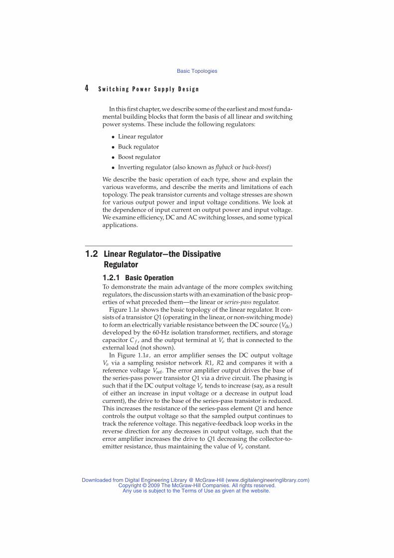
Figure 1.1a shows the basic topology of the linear regulator. It con-sists of a transistor Q1 (operating in the linear, or non-switching mode)to form an electrically variable resistance between the DC source (Vdc)developed by the 60-Hz isolation transformer, rectifiers, and storagecapacitor C f , and the output terminal at Vo that is connected to theexternal load (not shown).
In Figure 1.1a, an error amplifier senses the DC output voltageVo via a sampling resistor network R1, R2 and compares it with areference voltage Vref. The error amplifier output drives the base ofthe series-pass power transistor Q1 via a drive circuit. The phasing issuch that if the DC output voltage Vo tends to increase (say, as a resultof either an increase in input voltage or a decrease in output loadcurrent), the drive to the base of the series-pass transistor is reduced.This increases the resistance of the series-pass element Q1 and hencecontrols the output voltage so that the sampled output continues totrack the reference voltage. This negative-feedback loop works in thereverse direction for any decreases in output voltage, such that theerror amplifier increases the drive to Q1 decreasing the collector-to-emitter resistance, thus maintaining the value of Vo constant.
Downloaded from Digital Engineering Library @ McGraw-Hill (www.digitalengineeringlibrary.com)Copyright © 2009 The McGraw-Hill Companies. All rights reserved.
Any use is subject to the Terms of Use as given at the website.
Basic Topologies
C h a p t e r 1 : B a s i c T o p o l o g i e s 5
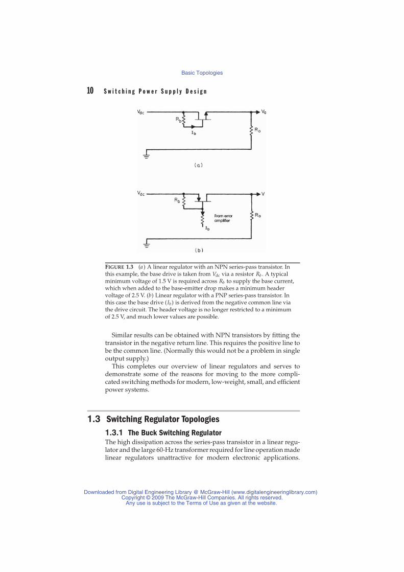
FIGURE 1.1 (a ) The linear regulator. The waveform shows the ripplenormally present on the unregulated DC input (Vdc). Transistor Q1, betweenthe DC source at Cf and the output load at Vo , acts as an electrically variableresistance. The negative-feedback loop via the error amplifier alters theeffective resistance of Q1 and will keep Vo constant, providing the inputvoltage sufficiently exceeds the output voltage. (b) Figure 1.1b shows theminimum input-output voltage differential (or headroom) required in a linearregulator. With a typical NPN series-pass transistor, a minimum input-outputvoltage differential (headroom) of at least 2.5 V is required between Vo andthe bottom of the C f input ripple waveform at minimum Vac input.
In general, any change in input voltage—due to, for example, ACinput line voltage change, ripple, steady-state changes in the input oroutput, and any dynamic changes resulting from rapid load changesover its designed tolerance band—is absorbed across the series-passelement. This maintains the output voltage constant to an extent de-termined by the gain in the open-loop feedback amplifier.
Switching regulators have transformers and fast switching actionsthat can cause considerable RFI noise. However, in the linear regulatorthe feedback loop is entirely DC-coupled. There are no switching ac-tions within the loop. As a result, all DC voltage levels are predictableand calculable. This lower RFI noise can be a major advantage in someapplications, and for this reason, linear regulators still have a place inmodern power supply applications even though the efficiency is quitelow. Also since the power losses are mainly due to the DC current andthe voltage across Q1, the loss and the overall efficiency are easilycalculated.
Downloaded from Digital Engineering Library @ McGraw-Hill (www.digitalengineeringlibrary.com)Copyright © 2009 The McGraw-Hill Companies. All rights reserved.
Any use is subject to the Terms of Use as given at the website.
Basic Topologies

6 S w i t c h i n g P o w e r S u p p l y D e s i g n
1.2.2 Some Limitations of the Linear RegulatorThis simple, DC-coupled series-pass linear regulator was the basisfor a multi-billion-dollar power supply industry until the early 1960s.However, in simple terms, it has the following limitations:
• The linear regulator is constrained to produce only a lower reg-ulated voltage from a higher non-regulated input.
• The output always has one terminal that is common with theinput. This can be a problem, complicating the design whenDC isolation is required between input and output or betweenmultiple outputs.
• The raw DC input voltage (Vdc in Figure 1.1a ) is usually de-rived from the rectified secondary of a 60-Hz transformer whoseweight and volume was often a serious system constraint.
• As shown next, the regulation efficiency is very low, resulting ina considerable power loss needing large heat sinks in relativelylarge and heavy power units.
1.2.3 Power Dissipation in the Series-Pass TransistorA major limitation of a linear regulator is the inevitable and large dis-sipation in the series-pass element. It is clear that all the load currentmust pass through the pass transistor Q1, and its dissipation will be(Vdc − Vo )( Io ). The minimum differential (Vdc − Vo ), the headroom,is typically 2.5 V for NPN pass transistors. Assume for now that thefilter capacitor is large enough to yield insignificant ripple. Typicallythe raw DC input comes from the rectified secondary of a 60-Hz trans-former. In this case the secondary turns can always be chosen so thatthe rectified secondary voltage is near Vo + 2.5 V when the input ACis at its low tolerance limit. At this point the dissipation in Q1 will bequite low.
However, when the input AC voltage is at its high tolerance limit,the voltage across Q1 will be much greater, and its dissipation willbe larger, reducing the power supply efficiency. Due to the minimum2.5-volt headroom requirement, this effect is much more pronouncedat lower output voltages.
This effect is dramatically demonstrated in the following examples.We will assume an AC input voltage range of ±15%. Consider threeexamples as follows:
• Output of 5 V at 10 A
• Output of 15 V at 10 A
• Output of 30 V at 10 A
Downloaded from Digital Engineering Library @ McGraw-Hill (www.digitalengineeringlibrary.com)Copyright © 2009 The McGraw-Hill Companies. All rights reserved.
Any use is subject to the Terms of Use as given at the website.
Basic Topologies

C h a p t e r 1 : B a s i c T o p o l o g i e s 7
Assume for now that a large secondary filter capacitor is used such thatripple voltage to the regulator is negligible. The rectified secondaryvoltage range (Vdc) will be identical to the AC input voltage range of±15%. The transformer secondary voltages will be chosen to yield(Vo + 2.5 V) when the AC input is at its low tolerance limit of−15%. Hence, the maximum DC input is 35% higher when the ACinput is at its maximum tolerance limit of +15%. This yields thefollowing:
Vdc(min)′ Vdc(max)′ Headroom, Pin(max)′ Pout(max)′ Dissipation Efficiency, %Vo Io , A V V max, V W W Q1max Po /Pin(max)
5.0 10 7.5 10.1 5.1 101 50 51 50
15.0 10 17.5 23.7 8.7 237 150 87 63
30.0 10 32.5 44.0 14 440 300 140 68
It is clear from this example that at lower DC output voltages theefficiency will be very low. In fact, as shown next, when realistic inputline ripple voltages are included, the efficiency for a 5-volt output witha line voltage range of ±15% will be only 32 to 35%.
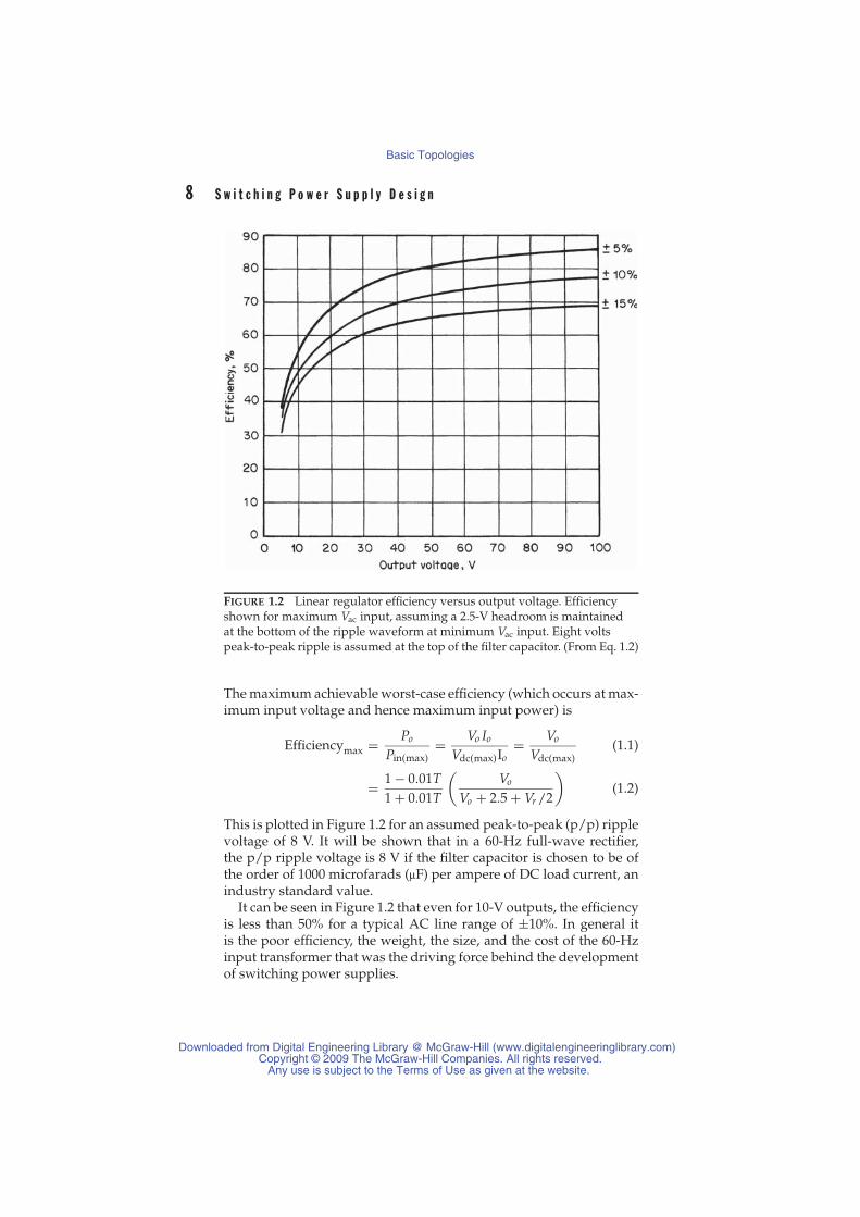
1.2.4 Linear Regulator Efficiency vs. Output VoltageWe will consider in general the range of efficiency expected for a rangeof output voltages from 5 V to 100 V with line inputs ranging from±5 to ±15% when a realistic ripple value is included.
Assume the minimum headroom is to be 2.5 V, and this must beguaranteed at the bottom of the input ripple waveform at the lowerlimit of the input AC voltages range, as shown in Figure 1.1b. Regula-tor efficiency can be calculated as follows for various assumed inputAC tolerances and output voltages.
Let the input voltage range be ±T% about its nominal. The trans-former secondary turns will be selected so that the voltage at thebottom of the ripple waveform will be 2.5 V above the desired outputvoltage when the AC input is at its lower limit.
Let the peak-to-peak ripple voltage be Vr volts. When the input ACis at its low tolerance limit, the average or DC voltage at the input tothe pass transistor will be
Vdc = (Vo + 2.5 + Vr/2) volts
When the AC input is at its high tolerance limit, the DC voltage at theinput to the series-pass element is
Vdc(max) = 1 + 0.01T1 − 0.01T
(Vo + 2.5 + Vr /2)
Downloaded from Digital Engineering Library @ McGraw-Hill (www.digitalengineeringlibrary.com)Copyright © 2009 The McGraw-Hill Companies. All rights reserved.
Any use is subject to the Terms of Use as given at the website.
Basic Topologies
8 S w i t c h i n g P o w e r S u p p l y D e s i g n
FIGURE 1.2 Linear regulator efficiency versus output voltage. Efficiencyshown for maximum Vac input, assuming a 2.5-V headroom is maintainedat the bottom of the ripple waveform at minimum Vac input. Eight voltspeak-to-peak ripple is assumed at the top of the filter capacitor. (From Eq. 1.2)
The maximum achievable worst-case efficiency (which occurs at max-imum input voltage and hence maximum input power) is
Efficiencymax = Po
Pin(max)= Vo Io
Vdc(max)Io= Vo
Vdc(max)(1.1)
= 1 − 0.01T1 + 0.01T
(Vo
Vo + 2.5 + Vr /2
)(1.2)
This is plotted in Figure 1.2 for an assumed peak-to-peak (p/p) ripplevoltage of 8 V. It will be shown that in a 60-Hz full-wave rectifier,the p/p ripple voltage is 8 V if the filter capacitor is chosen to be ofthe order of 1000 microfarads (μF) per ampere of DC load current, anindustry standard value.
It can be seen in Figure 1.2 that even for 10-V outputs, the efficiencyis less than 50% for a typical AC line range of ±10%. In general itis the poor efficiency, the weight, the size, and the cost of the 60-Hzinput transformer that was the driving force behind the developmentof switching power supplies.
Downloaded from Digital Engineering Library @ McGraw-Hill (www.digitalengineeringlibrary.com)Copyright © 2009 The McGraw-Hill Companies. All rights reserved.
Any use is subject to the Terms of Use as given at the website.
Basic Topologies
C h a p t e r 1 : B a s i c T o p o l o g i e s 9
However, the linear regulator with its lower electrical noise still hasapplications and may not have excessive power loss. For example,if a reasonably pre-regulated input is available (frequently the casein some of the switching configurations to be shown later), a linerregulator is a reasonable choice where lower noise is required. Com-plete integrated-circuit linear regulators are available up to 3-A outputin single plastic packages and up to 5 A in metal-case integrated-circuit packages. However, the dissipation across the internal series-pass transistor can still become a problem at the higher currents. Wenow show some methods of reducing the dissipation.
1.2.5 Linear Regulators with PNP Series-PassTransistors for Reduced Dissipation
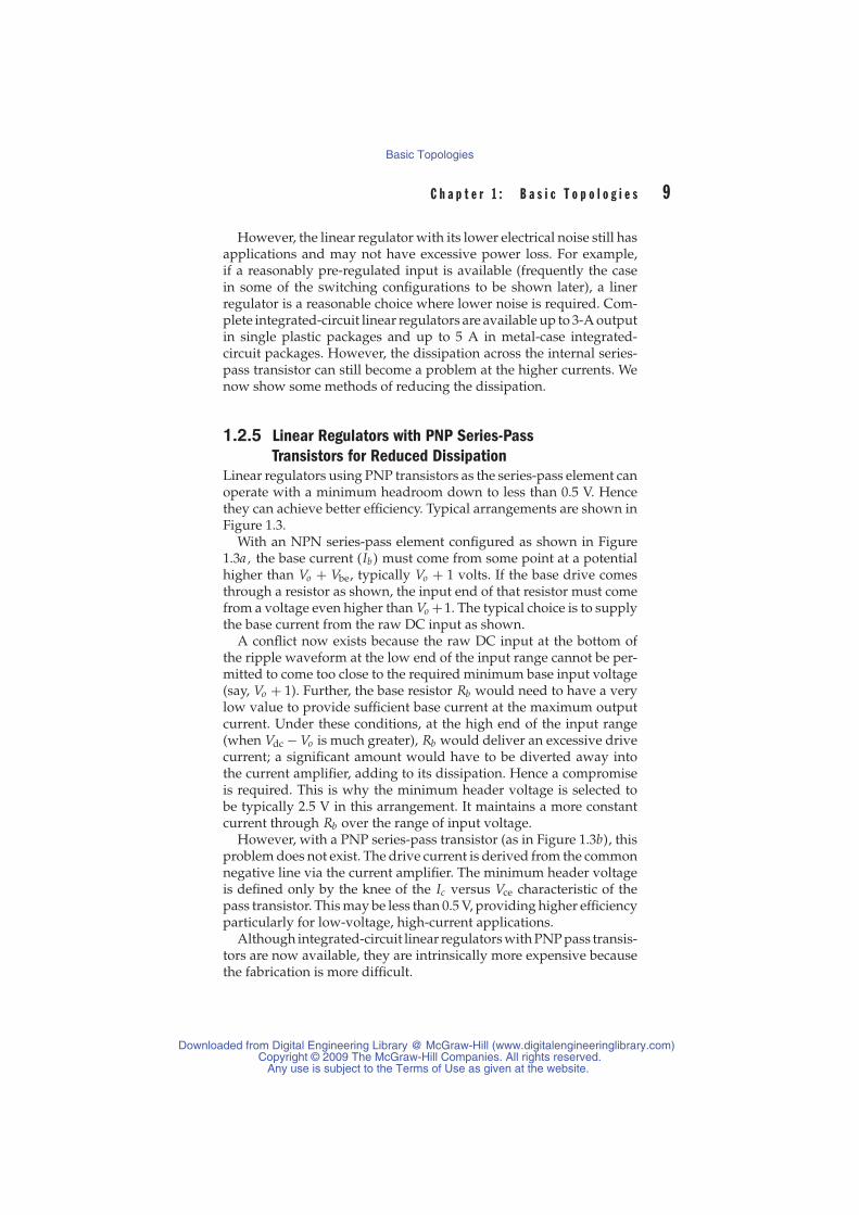
Linear regulators using PNP transistors as the series-pass element canoperate with a minimum headroom down to less than 0.5 V. Hencethey can achieve better efficiency. Typical arrangements are shown inFigure 1.3.
With an NPN series-pass element configured as shown in Figure1.3a, the base current (Ib) must come from some point at a potentialhigher than Vo + Vbe, typically Vo + 1 volts. If the base drive comesthrough a resistor as shown, the input end of that resistor must comefrom a voltage even higher than Vo +1. The typical choice is to supplythe base current from the raw DC input as shown.
A conflict now exists because the raw DC input at the bottom ofthe ripple waveform at the low end of the input range cannot be per-mitted to come too close to the required minimum base input voltage(say, Vo + 1). Further, the base resistor Rb would need to have a verylow value to provide sufficient base current at the maximum outputcurrent. Under these conditions, at the high end of the input range(when Vdc − Vo is much greater), Rb would deliver an excessive drivecurrent; a significant amount would have to be diverted away intothe current amplifier, adding to its dissipation. Hence a compromiseis required. This is why the minimum header voltage is selected tobe typically 2.5 V in this arrangement. It maintains a more constantcurrent through Rb over the range of input voltage.
However, with a PNP series-pass transistor (as in Figure 1.3b), thisproblem does not exist. The drive current is derived from the commonnegative line via the current amplifier. The minimum header voltageis defined only by the knee of the Ic versus Vce characteristic of thepass transistor. This may be less than 0.5 V, providing higher efficiencyparticularly for low-voltage, high-current applications.
Although integrated-circuit linear regulators with PNP pass transis-tors are now available, they are intrinsically more expensive becausethe fabrication is more difficult.
Downloaded from Digital Engineering Library @ McGraw-Hill (www.digitalengineeringlibrary.com)Copyright © 2009 The McGraw-Hill Companies. All rights reserved.
Any use is subject to the Terms of Use as given at the website.
Basic Topologies
10 S w i t c h i n g P o w e r S u p p l y D e s i g n
FIGURE 1.3 (a ) A linear regulator with an NPN series-pass transistor. Inthis example, the base drive is taken from Vdc via a resistor Rb . A typicalminimum voltage of 1.5 V is required across Rb to supply the base current,which when added to the base-emitter drop makes a minimum headervoltage of 2.5 V. (b) Linear regulator with a PNP series-pass transistor. Inthis case the base drive (Ib) is derived from the negative common line viathe drive circuit. The header voltage is no longer restricted to a minimumof 2.5 V, and much lower values are possible.
Similar results can be obtained with NPN transistors by fitting thetransistor in the negative return line. This requires the positive line tobe the common line. (Normally this would not be a problem in singleoutput supply.)
This completes our overview of linear regulators and serves todemonstrate some of the reasons for moving to the more compli-cated switching methods for modern, low-weight, small, and efficientpower systems.
1.3 Switching Regulator Topologies1.3.1 The Buck Switching RegulatorThe high dissipation across the series-pass transistor in a linear regu-lator and the large 60-Hz transformer required for line operation madelinear regulators unattractive for modern electronic applications.
Downloaded from Digital Engineering Library @ McGraw-Hill (www.digitalengineeringlibrary.com)Copyright © 2009 The McGraw-Hill Companies. All rights reserved.
Any use is subject to the Terms of Use as given at the website.
Basic Topologies

C h a p t e r 1 : B a s i c T o p o l o g i e s 11
Further, the high power loss in the series device requires a large heatsink and large storage capacitors and makes the linear power supplydisproportionately large.
As electronics advanced, integrated circuits made the electronic sys-tems smaller. Typically, linear regulators could achieve output powerdensities of 0.2 to 0.3 W/in3, and this was not good enough for theever smaller modern electronic systems. Further, linear power sup-plies could not provide the extended hold-up time required for thecontrolled shutdown of digital storage systems.
Although the technology was previously well known, switchingregulators started being widely used as alternatives to linear reg-ulators only in the early 1960s when suitable semiconductors withreasonable performance and cost became available. Typically thesenew switching supplies used a transistor switch to generate a square-waveform from a non-regulated DC input voltage. This square wave,with adjustable duty cycle, was applied to a low pass output powerfilter so as to provide a regulated DC output.
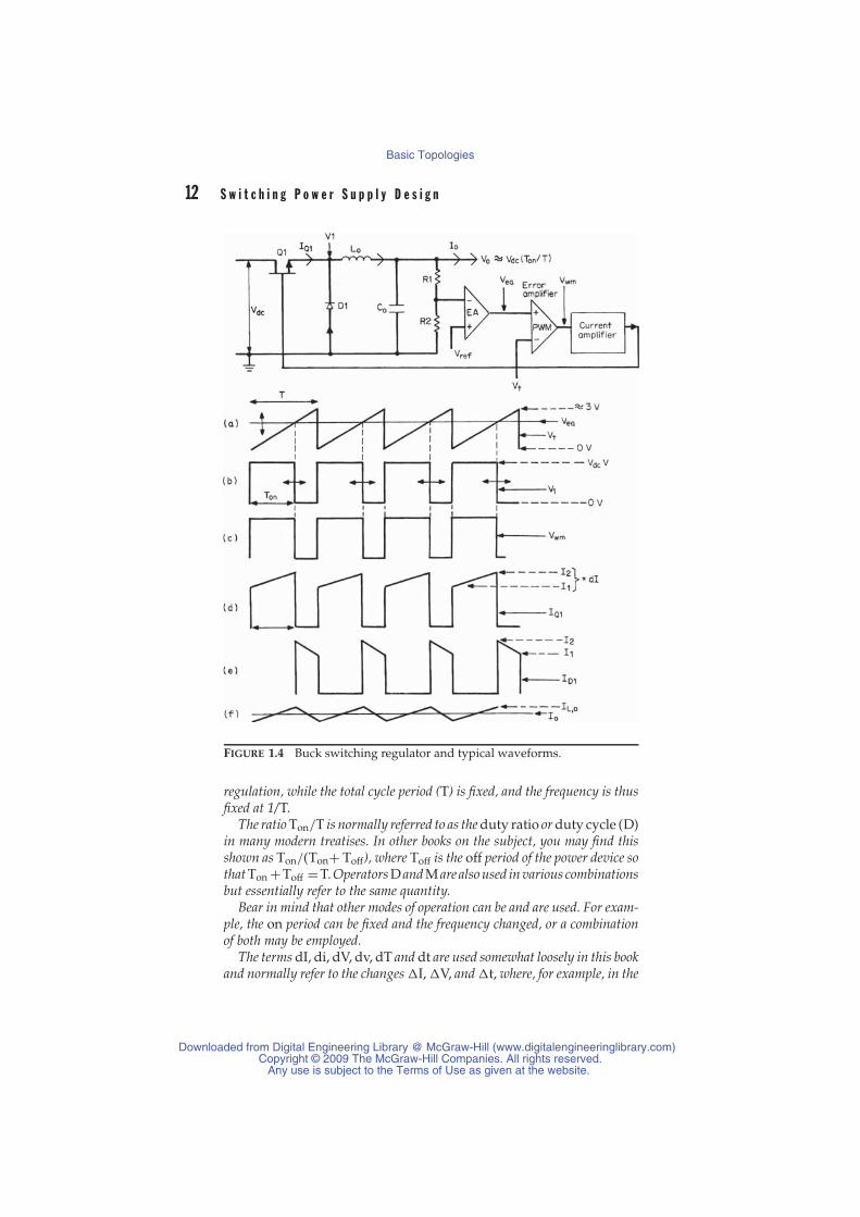
Usually the filter would be an inductor (or more correctly a choke,since it had to support some DC) and an output capacitor. By varyingthe duty cycle, the average DC voltage developed across the outputcapacitor could be controlled. The low pass filter ensured that the DCoutput voltage would be the average value of the rectangular voltagepulses (of adjustable duty cycle) as applied to the input of the low passfilter. A typical topology and waveforms are shown later in Figure 1.4.
With appropriately chosen low pass inductor/capacitor (LC) fil-ters, the square-wave modulation could be effectively minimized, andnear-ripple-free DC output voltages, equal to the average value ofthe duty-cycle-modulated raw DC input, could be provided. By sens-ing the DC output voltage and controlling the switch duty cycle ina negative-feedback loop, the DC output could be regulated againstinput line voltage changes and output load changes.
Modern very high frequency switching supplies are currentlyachieving up to 20 W/in3 compared with 0.3 W/in3 for the older linearpower supplies. Further, they are capable of generating a multiplicityof isolated output voltages from a single input. They do not require a50/60-Hz isolation power transformer, and they have efficiencies from70% up to 95%. Some DC/DC converter designers are claiming loadpower densities of up to 50 W/in3 for the actual switching elements.
1.3.1.1 Basic Elements and Waveforms of a Typical Buck Regulator
After Pressman In the interest of simplicity, Mr. Pressman describesfixed-frequency operation for the following switching regulator examples. Insuch regulators the on period of the power device (Ton) is adjusted to maintain
Downloaded from Digital Engineering Library @ McGraw-Hill (www.digitalengineeringlibrary.com)Copyright © 2009 The McGraw-Hill Companies. All rights reserved.
Any use is subject to the Terms of Use as given at the website.
Basic Topologies
12 S w i t c h i n g P o w e r S u p p l y D e s i g n
FIGURE 1.4 Buck switching regulator and typical waveforms.
regulation, while the total cycle period (T) is fixed, and the frequency is thusfixed at 1/T.
The ratio Ton/T is normally referred to as the duty ratio or duty cycle (D)in many modern treatises. In other books on the subject, you may find thisshown as Ton/(Ton+ Toff), where Toff is the off period of the power device sothat Ton +Toff =T. Operators D and M are also used in various combinationsbut essentially refer to the same quantity.
Bear in mind that other modes of operation can be and are used. For exam-ple, the on period can be fixed and the frequency changed, or a combinationof both may be employed.
The terms dI, di, dV, dv, dT and dt are used somewhat loosely in this bookand normally refer to the changes �I, �V, and �t, where, for example, in the
Downloaded from Digital Engineering Library @ McGraw-Hill (www.digitalengineeringlibrary.com)Copyright © 2009 The McGraw-Hill Companies. All rights reserved.
Any use is subject to the Terms of Use as given at the website.
Basic Topologies

C h a p t e r 1 : B a s i c T o p o l o g i e s 13
limit, �I/�t goes to the derivative di/dt, giving the rate of change of currentwith time or the slope of the waveform. Since in most cases the waveformslopes are linear the result is the same so this becomes a moot point. ∼K.B.
1.3.1.2 Buck Regulator Basic OperationThe basic elements of the buck regulator are shown in Figure 1.4.Transistor Q1 is switched hard “on” and hard “off” in series with theDC input Vdc to produce a rectangular voltage at point V1. For fixed-frequency duty-cycle control, Q1 conducts for a time Ton (a small partof the total switching period T). When Q1 is “on,” the voltage at V1 isVdc, assuming for the moment the “on” voltage drop across Q1 is zero.
A current builds up in the series inductor Lo flowing toward the out-put. When Q1 turns “off,” the voltage at V1 is driven rapidly towardground by the current flowing in inductor Lo and will go negative un-til it is caught and clamped at about −0.8 V by diode D1 (the so-calledfree-wheeling diode).
Assume for the moment that the “on” drop of diode D1 is zero. Thesquare voltage shown in Figure 1.4b would be rectangular, rangingbetween Vdc and ground, (0 V) with a “high” period of Ton. The averagevalue of this rectangular waveform is VdcTon/T. The low pass LoCofilter in series between V1 and the output V extracts the DC componentand yields a clean, near-ripple-free DC voltage at the output with amagnitude Vo of VdcTon/T.
To control the voltage, Vo is sensed by sampling resistors R1 and R2and compared with a reference voltage Vref in the error amplifier (EA).The amplified DC error voltage Vea is fed to a pulse-width-modulator(PWM). In this example the PWM is essentially a voltage compara-tor with a sawtooth waveform as the other input (see Figure 1.4a ).This sawtooth waveform has a period T and amplitude typically inthe order of 3 V. The high-gain PWM voltage comparator generates arectangular output waveform (Vwm, see Figure 1.4c) that goes high atthe start of the sawtooth ramp, and goes low the instant the ramp volt-age crosses the DC voltage level from the error-amplifier output. ThePWM output pulse width (Ton) is thus controlled by the EA amplifieroutput voltage.
The PWM output pulse is fed to a driver circuit and used to controlthe “on” time of transistor switch Q1 inside the negative-feedbackloop. The phasing is such that if Vdc goes slightly higher, the EA DClevel goes closer to the bottom of the ramp, the ramp crosses the EAoutput level earlier, and the Q1 “on” time decreases, maintaining theoutput voltage constant. Similarly, if Vdc is reduced, the “on” time ofQ1 increases to maintain Vo constant. In general, for all changes, the“on” time of Q1 is controlled so as to make the sampled DC outputvoltage Vo R2/(R1 + R2) closely track the reference voltage Vref.
Downloaded from Digital Engineering Library @ McGraw-Hill (www.digitalengineeringlibrary.com)Copyright © 2009 The McGraw-Hill Companies. All rights reserved.
Any use is subject to the Terms of Use as given at the website.
Basic Topologies

14 S w i t c h i n g P o w e r S u p p l y D e s i g n
1.3.2 Typical Waveforms in the Buck RegulatorIn general, the major advantage of the switching regulator techniqueover its linear counterpart is the elimination of the power loss intrinsicin the linear regulator pass element.
In the switching regulator the pass element is either fully “on” (withvery little power loss) or fully “off” (with negligible power loss). Thebuck regulator is a good example of this—it has low internal lossesand hence high power conversion efficiency.
However, to fully appreciate the subtleties of its operation, it isnecessary to understand the waveforms and the magnitude and tim-ing of the currents and voltages throughout the circuit. To this endwe will look in more detail at a full cycle of events starting whenQ1 turns fully “on.” For convenience we will assume ideal compo-nents and steady-state conditions, with the amplitude of the inputvoltage Vdc constant, exceeding the output voltage Vo , which is alsoconstant.
When Q1 turns fully “on,” the supply voltage Vdc will appear acrossthe diode D1 at point V1. Since the output voltage Vo is less than Vdc,the inductor Lo will have a voltage impressed across it of (Vdc − Vo ).With a constant voltage across the inductor, its current rises linearlyat a rate given by di/dt = (Vdc − Vo )/Lo . (This is shown in Figure 1.4das a ramp that sits on top of the step current waveform.)
When Q1 turns “off,” the voltage at point V1 is driven towardzero because it is not possible to change the previously establishedinductor current instantaneously. Hence the voltage polarity acrossLo immediately reverses, trying to maintain the previous current.(This polarity reversal is often referred to as the flyback or inductivekickback effect of the inductor.) Without diode D1, V1 would havegone very far negative, but with D1 fitted as shown, as the V1 volt-age passes through zero, D1 conducts and clamps the left side ofLo at one diode drop below ground. The voltage across the inductorhas now reversed, and the current in the inductor and D1 will rampdown, returning to its original starting value, during the “off” periodof Q1.
More precisely, when Q1 turns “off,” the current I2 (which hadbeen flowing in Q1, Lo and the output capacitor Co and the load justprior to turning “off”) is diverted and now flows through diode D1,Lo and the output capacitor and load, as shown in Figure 1.4e. Thevoltage polarity across Lo has reversed with a magnitude of (Vo + 1).The current in Lo now ramps down linearly at a rate defined by theequation di/dt = (Vo +1)/Lo . This is the downward ramp that sits on astep in Figure 1.4e. Under steady-state conditions, at the end of the Q1“off” time, the current in Lo will have fallen to I1 and is still flowingthrough D1, Lo and the output capacitor and load.
Downloaded from Digital Engineering Library @ McGraw-Hill (www.digitalengineeringlibrary.com)Copyright © 2009 The McGraw-Hill Companies. All rights reserved.
Any use is subject to the Terms of Use as given at the website.
Basic Topologies

C h a p t e r 1 : B a s i c T o p o l o g i e s 15
Note Notice the input current is discontinuous with a pulse-likecharacteristic, whereas the output current remains nearly continuous withsome relatively small ripple component depending on the value of Lo andCo . ∼ K.B.
Now when Q1 turns “on” again, it initially supplies current intothe cathode of D1, displacing its previous forward current. While thecurrent in Q1 rises toward the previous value of I1, the forward D1current will be displaced, and V1 rises to near Vdc, back-biasing D1.Because Q1 is switched “on” hard, this recovery process is very rapid,typically less than 1 μs.
Notice that the current in Lo is the sum of the Q1 current when itis “on” (see Figure 1.4d) plus the D1 current when Q1 is “off.” This isshown in Figure 1.4 f as IL,o . It has a DC component and a triangularwaveform ripple component (I2 − I1) centered on the mean DC out-put current Io . Thus the value of the current at the center of the rampin Figure 1.4d and 1.4e is simply the DC mean output current Io . Asthe load resistance and hence load current is changed, the center ofthe ramp (the mean value) in either Figure 1.4d or 1.4e moves, but theslopes of the ramps remain constant, because during the Q1 “on” time,the ramp rate in Lo remains the same at (Vdc − Vo )/Lo, and during theQ1 “off” time, it remains the same at (Vo + 1)/L as the load currentchanges, because the input and output voltages remain constant.
Because the p-p ripple current remains constant regardless of themean output current, it will be seen shortly that when the DC currentIo is reduced to the point where the lower value of the ripple currentin Figure 1.4d and 1.4e just reaches zero (the critical load current),there will be a drastic change in performance. (This will be discussedin more detail later.)
1.3.3 Buck Regulator EfficiencyTo get a general feel for the intrinsic power loss in the buck regulatorcompared with a linear regulator, we will start by assuming ideal com-ponents for transistor Q1 and diode D1 in both topologies. Using thecurrents shown in Figure 1.4d and 1.4e, the typical conduction lossesin Q1 and free-wheeling diode D1 can be calculated and the efficiencyobtained. Notice that when Q1 is “off,” it operates at a maximum volt-age of Vdc but at zero current. When Q1 is “on,” current flows, but thevoltage across Q1 is zero. At the same time, D1 is reverse-biased at avoltage of Vdc but has zero current. (Clearly, if Q1 and D1 were idealcomponents, the currents would flow through Q1 and D1 with zerovoltage drop, and the loss would be zero.)
Hence unlike the linear regulator, which has an intrinsic loss evenwith ideal components, the intrinsic loss in a switching regulator with
Downloaded from Digital Engineering Library @ McGraw-Hill (www.digitalengineeringlibrary.com)Copyright © 2009 The McGraw-Hill Companies. All rights reserved.
Any use is subject to the Terms of Use as given at the website.
Basic Topologies
16 S w i t c h i n g P o w e r S u p p l y D e s i g n
ideal components is zero, and the efficiency is 100%. Thus in the buckregulator, the real efficiency depends on the actual performance ofthe components. Since improvements are continually being made insemiconductors, we will see ever higher efficiencies.
To consider more realistic components, the losses in the buck circuitare the conduction losses in Q1 and D1 and the resistive winding lossin the choke. The conduction losses, being related to the mean DCcurrents, are relatively easy to calculate. To this we must add the ACswitching losses in Q1 and D1, and the AC induced core loss in theinductor, so the switching loss is more difficult to establish.
The switching loss in Q1 during the turn “on” and turn “off” tran-sitions is a result of the momentary overlap of current and voltageduring the switching transitions. Diode D1 also has switching lossassociated with the reverse recovery action of the diode, where againthere is a condition of voltage and current stress during the transitions.The ripple waveform in the inductor Lo results in hysteretic and eddycurrent loss in the core material. We will now calculate some typicallosses.
1.3.3.1 Calculating Conduction Loss andConduction-Related Efficiency
By neglecting second-order effects and AC switching losses, theconduction loss can be quite easily calculated. It can be seen fromFigure 1.4d and 1.4e that the average currents in Q1 and D1 duringtheir conduction times of Ton and Toff are the values at the center ofthe ramps or Io , the mean DC output current. These currents flow ata forward voltage of about 1 V over a wide range of currents. Thusconduction losses will be approximately
Pdc = L(Q1) + L(D1) = 1IoTon
T+ 1Io
Toff
T= 1Io
Therefore, by neglecting AC switching losses, the conduction-relatedefficiency would be
Conduction Efficiency = Po
Po + losses= Vo Io
Vo Io + 1Io= Vo
Vo + 1(1.3)
1.3.4 Buck Regulator Efficiency IncludingAC Switching Losses
After Pressman The switching loss is much more difficult to establish,because it depends on many variables relating to the performance of thesemiconductors and to the methods of driving the switching devices. Othervariables, related to the actual power circuit designs, include the action of any
Downloaded from Digital Engineering Library @ McGraw-Hill (www.digitalengineeringlibrary.com)Copyright © 2009 The McGraw-Hill Companies. All rights reserved.
Any use is subject to the Terms of Use as given at the website.
Basic Topologies
C h a p t e r 1 : B a s i c T o p o l o g i e s 17
snubbers, load line shaping, and energy recovery arrangements. It depends onwhat the designer may choose to use in a particular design. (See Chapter 11.)
Unless all these things are considered, any calculations are at best only avery rough approximation and can be far from the real values found in theactual design, particularly at high frequencies with the very fast switchingdevices now available.
After Pressman I leave Mr. Pressman’s original calculations, shownnext, untouched except for some minor editing, because they serve to il-lustrate the root cause of the switching loss. However, I would recommendthat the reader consider using more practical methods to establish the realloss. Many semiconductor manufacturers now provide switching loss equa-tions for their switching devices when recommended drive conditions areused, particularly the modern fast IGBTs (Insulated Gate Bipolar Transis-tors). Some fast digital oscilloscopes claim that they will actually measureswitching loss, providing the real-time device current and voltage is accu-rately provided to the oscilloscope. (Doing this can also be problematical atvery high frequency.)
The method I prefer, which is unquestionably accurate, is to measure thetemperature rise of the device in question in a working model. The modelmust include all the intended snubbers and load line shaping circuits, etc.Replacing the AC current in the device with a DC current to obtain the sametemperature rise will provide a direct indication of power loss by simple DCpower measurements. This method also allows easy optimization of the driveand load line shaping, which can be dynamically adjusted during operationfor minimum temperature rise and hence minimum switching loss. ∼ K.B.
Mr. Pressman continues as follows:
Alternating-current switching loss (or voltage/current overlap loss)calculation depends on the shape and timing of the rising and fallingvoltage and current waveforms. An idealized linear example—whichis unlikely to exist in practice—is shown in Figure 1.5a and serves toillustrate the principle.
Figure 1.5a shows the best-case scenario. At the turn “on” of theswitching device, the voltage and current start changing simulta-neously and reach their final values simultaneously. The currentwaveform goes from 0 to Io , and voltage across Q1 goes from a max-imum of Vdc down to zero. The average power during this switchingtransition is P(Ton) = ∫ Ton
0 IV dt = Io Vdc/6, and the power averagedover one complete period is (Io Vdc/6)(Ton/T).
Assuming the same scenario of simultaneous starting and endingpoints for the current fall and voltage rise waveforms at the turn “off”transition, the voltage/current overlap dissipation at this transitionis given by P(Toff) = ∫ Toff
0 IV dt = Io Vdc/6 and this power averagedover one complete cycle is (Io Vdc/6)(Toff/T).
Downloaded from Digital Engineering Library @ McGraw-Hill (www.digitalengineeringlibrary.com)Copyright © 2009 The McGraw-Hill Companies. All rights reserved.
Any use is subject to the Terms of Use as given at the website.
Basic Topologies
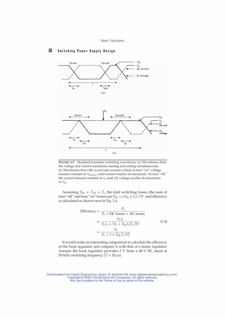
18 S w i t c h i n g P o w e r S u p p l y D e s i g n
FIGURE 1.5 Idealized transistor switching waveforms. (a ) Waveforms showthe voltage and current transitions starting and ending simultaneously.(b) Waveforms show the worst-case scenario, where at turn “on” voltageremains constant at Vdc(max) until current reaches its maximum. At turn “off,”the current remains constant at Io until Q1 voltage reaches its maximumof Vdc.
Assuming Ton = Toff = Ts , the total switching losses (the sum ofturn “off” and turn “on” losses) are Pac = (Vdc Io Ts)/3T, and efficiencyis calculated as shown next in Eq. 1.4.
Efficiency = Po
Po + DC losses + AC losses
= Vo Io
Vo Io + 1Io + Vdc Io Ts/3T(1.4)
= Vo
Vo + 1 + VdcTs/3T
It would make an interesting comparison to calculate the efficiencyof the buck regulator and compare it with that of a linear regulator.Assume the buck regulator provides 5 V from a 48-V DC input at50-kHz switching frequency (T = 20 μs).
Downloaded from Digital Engineering Library @ McGraw-Hill (www.digitalengineeringlibrary.com)Copyright © 2009 The McGraw-Hill Companies. All rights reserved.
Any use is subject to the Terms of Use as given at the website.
Basic Topologies

C h a p t e r 1 : B a s i c T o p o l o g i e s 19
If there were no AC switching losses and a switching transitionperiod Ts of 0.3 μs were assumed, Eq. 1.3 would give a conductionloss efficiency of
Efficiency = 55 + 1
= 83.3%
If switching losses for the best-case scenario as shown in Figure 1.5awere assumed, for Ts = 0.3 μs and T = 20 μs, Eq. 1.4 would give aswitching-related efficiency of
Efficiency = 55 + 1 + 48 × 0.3/3 × 20
= 55 + 1 + 0.24
= 55 + 1.24
= 80.1%
If a worst-case scenario were assumed (which is closer to reality),as shown in Figure 1.5b, efficiencies would lower. In Figure 1.5b it isassumed that at turn “on” the voltage across the transistor remainsat its maximum value (Vdc) until the on-turning current reaches itsmaximum value of Io . Then the voltage starts falling. To a close ap-proximation, the current rise time Tcr will equal voltage fall time. Thenthe turn “on” switching losses will be
P(Ton) = Vde Io
2Tcr
T+ Io Vdc
2Tvf
T
also for Tcr = Tvf = Ts , P(Ton) = Vdc Io (Ts/T).At turn “off” (as seen in Figure 1.5b), we may assume that current
hangs on at this maximum value Io until the voltage has risen to itsmaximum value of Vdc in a time Tvr. Then current starts falling andreaches zero in a time Tcf. The total turn “off” dissipation will be
P(Toff) = Io Vdc
2Tvr
T+ Vdc Io
2Tcf
T
With Tvr = Tcf = Ts , P(Toff) = Vdc Io (Ts/T). The total AC losses (thesum of the turn “on” plus the turn “off” losses) will be
Pac = 2Vdc IoTs
T(1.5)
and the total losses (the sum of DC plus AC losses) will be
Pt = Pdc + Pac = 1Io + 2Vdc IoTs
T(1.6)
Downloaded from Digital Engineering Library @ McGraw-Hill (www.digitalengineeringlibrary.com)Copyright © 2009 The McGraw-Hill Companies. All rights reserved.
Any use is subject to the Terms of Use as given at the website.
Basic Topologies

20 S w i t c h i n g P o w e r S u p p l y D e s i g n
and the efficiency will be
Efficiency = Po
Po + Pt= Vo Io
Vo Io + 1Io + 2Vdc Io Ts/T
= Vo
Vo + 1 + 2VdcTs/T(1.7)
Hence in the worst-case scenario, for the same buck regulator withTs = 0.3 μs, the efficiency from Eq. 1.7 will be
Efficiency = 55 + 1 + 2 × 48 × 0.3/20
= 55 + 1 + 1.44
= 55 + 1 + 2.44
= 67.2%
Comparing this with a linear regulator doing the same job (bringing48 V down to 5 V), its efficiency (from Eq. 1.1) would be Vo/Vdc(max),or 5/48; this is only 10.4% and is clearly unacceptable.
1.3.5 Selecting the OptimumSwitching Frequency
We have seen that the output voltage of the buck regulator is givenby the equation Vo = VdcTon/T. We must now decide on a value forthis period and hence the operating frequency.
The initial reaction may be to minimize the size of the filter compo-nents Lo , Co by using as high a frequency as possible. However, usinghigher frequencies does not necessarily minimize the overall size ofthe regulator when all factors are considered.
We can see this better by examining the expression for the AC lossesshown in Eq. 1.5, Pac = 2Vdc Io
TsT . We see that the AC losses are in-
versely proportional to the switching period T . Further, this equationonly shows the losses in the switching transistor; it neglects lossesin the free-wheeling diode D1 due to its finite reverse recovery time(the time required for the diode to cease conducting reverse current,measured from the instant it has been subjected to a reverse bias volt-age). The free-wheeling diode can dissipate significant power andshould be of the ultrafast soft recovery type with minimum recoveredcharge. The reverse recovery time will typically be 35 ns or less.
In simple terms, the more switching transitions there are in a partic-ular period, the more switching loss there will be. As a result there is atrade-off—decreasing the switching period T (increasing the switch-ing frequency) may well decrease the size of the filter elements, but itwill also add to the total losses and may require a larger heat sink.
Downloaded from Digital Engineering Library @ McGraw-Hill (www.digitalengineeringlibrary.com)Copyright © 2009 The McGraw-Hill Companies. All rights reserved.
Any use is subject to the Terms of Use as given at the website.
Basic Topologies

C h a p t e r 1 : B a s i c T o p o l o g i e s 21
In general, although the overall volume of the buck regulator willbe lower at a higher frequency, the increase in the switching loss andthe more stringent high-frequency layout and component-selectionrequirements make the final choice a compromise among all the op-posing elements.
Note The picture is constantly changing as better, lower cost, and fastertransistors and diodes are developed. My choice at the present stage of thetechnology is to design below 100 kHz, as this is less demanding on componentselection, layout, and transformer/inductor designs. As a result it is probablylower cost. Generally speaking, higher frequencies absorb more developmenttime and require more experience. However, efficient commercial designs areon the market operating well into the MHz range. The final choice is upto the designer, and I hesitate to recommend a limit because technology isconstantly changing toward higher frequency operation. ∼ K.B.
1.3.6 Design Examples1.3.6.1 Buck Regulator Output Filter Inductor (Choke) Design
Note The output inductor and capacitor may be considered a low passfilter, and it is normally treated in this way for transfer function and loopcompensation calculations.
However, at this stage, the reader may prefer to look upon the inductor asa device that tends to maintain the current reasonably constant during theswitching action. (That is, it stores energy when the power device is “on”and transfers this energy to the output when the power device is “off.”)
I prefer the term choke for the power inductor, because in this applicationit must support an element of DC current as well as the applied AC voltagestress. It will be shown later (Chapter 7) that the design of pure inductors(with zero DC current component) is quite different from the design of chokes,with their relatively large DC current component.
In the following section Mr. Pressman outlines the parameters that controlthe design and selection of this critical part. ∼ K.B.
The current waveform of the output inductor (choke) is shown inFigure 1.4 f , and its characteristic “dual ramp” shape is defined inSection 1.3.2. Notice that the current amplitude at the center of theramp is the mean value equal to the DC output current Io .
We have seen that as the DC output load current decreases, the slopeof the ramp remains constant (because the voltage across Lo remainsconstant). But as the mean load current decreases, the ripple currentwaveform moves down toward zero.
At a load current of half the peak-to-peak magnitude of the ramp,Io = ( I2 − I1)/2dI, the lower point of the ramp just touches zero.
Downloaded from Digital Engineering Library @ McGraw-Hill (www.digitalengineeringlibrary.com)Copyright © 2009 The McGraw-Hill Companies. All rights reserved.
Any use is subject to the Terms of Use as given at the website.
Basic Topologies

22 S w i t c h i n g P o w e r S u p p l y D e s i g n
At this point, the current in the inductor is zero and its stored energyis zero. (The inductor is said to have “run dry.”) If the load currentis further reduced, there will be a period when the inductor currentremains at zero for a longer period and the buck regulator enters intothe “discontinuous current” operating mode. This is an importanttransition because a drastic change occurs in the current and voltagewaveforms and in the closed loop transfer function.
This transition to the discontinuous mode can be seen in the real-time oscilloscope picture of Figure 1.6a . This shows the power switchcurrent waveforms for a buck regulator operating at 25 kHz with aninput voltage of 20 V and an output of 5 V as the load current isreduced from a nominal current of 5 A down to about 0.2 A.
The top two waveforms have the characteristic ramp-on-a-stepwaveshape with the step size reducing as the load current is reduced.The current amplitude at the center of the ramp indicates the effectiveDC output current.
In the third waveform, where Io = 0.95 A, the step has gone andthe front end of the ramp starts at zero current. This is the critical loadcurrent indicating the start of the discontinuous current mode (or run-dry mode) for the inductor. Notice that in the first three waveforms,the Q1 “on” time is constant, but decreases drastically as the currentis further reduced, moving deeper into the discontinuous mode.
In this example, the control loop has been able to maintain the out-put voltage constant at 5 V throughout the full range of load currents,even after the inductor has gone discontinuous. Hence it would beeasy to assume that there is no problem in permitting the inductorto go discontinuous. In fact there are changes in the transfer function(discussed next) that the control loop must be able to accommodate.Further, the transition can become a major problem in the boost-typetopologies discussed later.
For the buck regulator, however, the discontinuous mode is notconsidered a major problem. For load currents above the onset of thediscontinuous made, the DC output voltage is given by Vo = V1Ton/T.
Notice the load current is not a parameter in this equation, so thevoltage remains constant with load current changes without the needto change the duty ratio. (The effective output resistance of the buckregulator is very low in this region.) In practice the “on” time changesslightly as the current changes, because the forward drop across Q1and the inductor resistance change slightly with current, requiring asmall change in Ton.
If the load is further reduced so as to enter discontinuous mode, thetransfer function changes drastically and the previous equation foroutput voltage (Vo = V1Ton/T) no longer applies. This can be seen inthe bottom two waveforms of Figure 1.6a . Notice the “on” time of Q1has decreased and has become a function of the DC output current.
Downloaded from Digital Engineering Library @ McGraw-Hill (www.digitalengineeringlibrary.com)Copyright © 2009 The McGraw-Hill Companies. All rights reserved.
Any use is subject to the Terms of Use as given at the website.
Basic Topologies
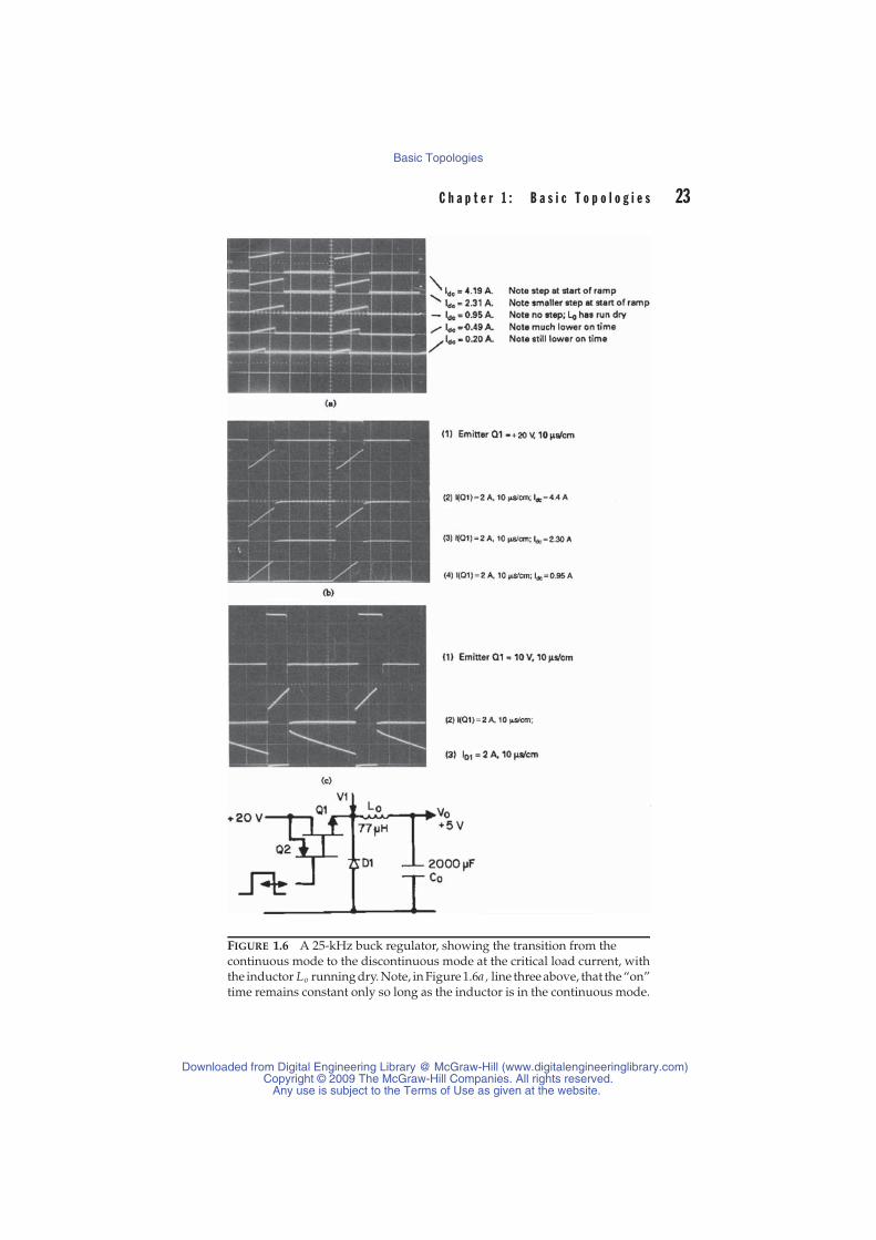
C h a p t e r 1 : B a s i c T o p o l o g i e s 23
FIGURE 1.6 A 25-kHz buck regulator, showing the transition from thecontinuous mode to the discontinuous mode at the critical load current, withthe inductor Lo running dry. Note, in Figure 1.6a, line three above, that the “on”time remains constant only so long as the inductor is in the continuous mode.
Downloaded from Digital Engineering Library @ McGraw-Hill (www.digitalengineeringlibrary.com)Copyright © 2009 The McGraw-Hill Companies. All rights reserved.
Any use is subject to the Terms of Use as given at the website.
Basic Topologies

24 S w i t c h i n g P o w e r S u p p l y D e s i g n
TIP The ratio Ton/T is normally referred to as the duty ratio D. The voltageformula for continuous operation is simply Vo = V1.D. However, for dis-continuous operation, the duty ratio becomes a function of the load current,and the situation is much more complicated. In the discontinuous mode, theoutput voltage Vo is given by the formula
Vo = V1.2DD + (D2 + (8L/RT))1/2
Since the control loop will maintain the output voltage constant, the effec-tive value of the load resistance R will be inversely proportional to the loadcurrent. Hence by holding Vo, V1, L, and T constant, to maintain the voltageconstant, requires that the remaining variable (the duty ratio D) must changewith load current.
At the critical transition current, the transfer function will change fromcontinuous mode in which the duty ratio remained constant with load change(zero output impedance) to the discontinuous mode in which the duty ratiomust change with reducing load current (a finite output impedance). Hencein the discontinuous mode, the control loop must work much harder, and thetransient performance will be degraded. ∼ K.B.
Dynamically, at load currents above the onset of the discontinu-ous mode, the output L/C filter automatically accommodated out-put current changers by changing the amplitude of the step part ofthe ramp-on-step waveforms shown in the Q1 and D1 waveforms ofFigures 1.4d and 1.4e. To the first order, it could do this without chang-ing the Q1 “on” time.
The DC output current is the time average of the Q1 and D1 rampcurrent. Notice that in Figure 1.6a, line three and line four, that at lowercurrents where the inductor has gone discontinuous and the step partof the latter waveforms has gone to zero, the only way the currentcan decrease further is to decrease the Q1 “on” time. The negative-feedback loop automatically adjusts the duty ratio to achieve this.
The dramatic change in the waveforms can be seen very clearlybetween Figure 1.7a (for the critical current condition) and Figure 1.7b(for the discontinuous condition). Figure 1.7b(2) shows the D1 currentgoing to zero just before Q1 turns “on” (the inductor has dried out andgone discontinuous). With zero current in Lo , the output voltage willseek to appear at the emitter of Q1. However, the sudden transitionresults in a decaying voltage “ring,” at a frequency determined by Loand the distributed capacitance looking into the D1 cathode and Q1emitter junction at point V1. This is shown in Figure 1.7b(1).
TIP Although the voltage ring is not damaging, in the interest of RFIreduction, it should be suppressed by a small R/C snubber across D1. ∼ K.B.
Downloaded from Digital Engineering Library @ McGraw-Hill (www.digitalengineeringlibrary.com)Copyright © 2009 The McGraw-Hill Companies. All rights reserved.
Any use is subject to the Terms of Use as given at the website.
Basic Topologies
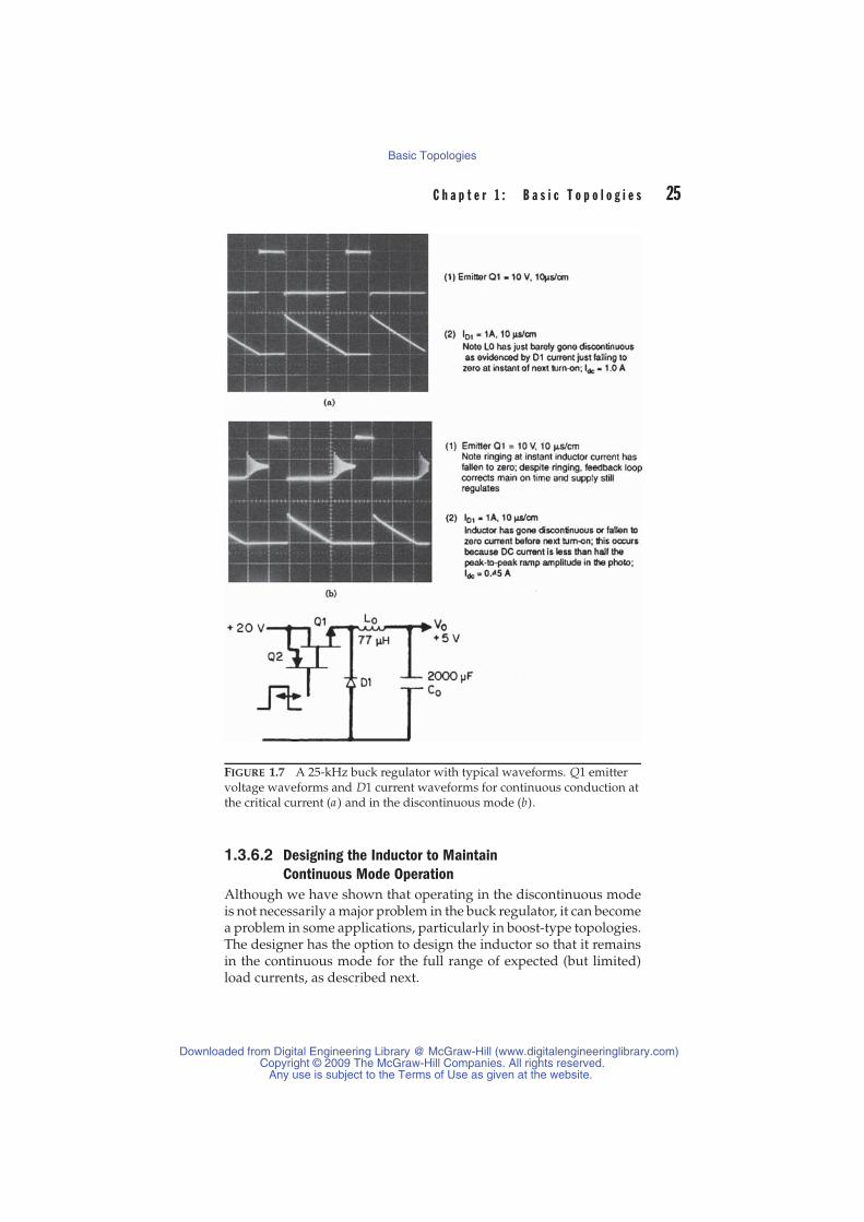
C h a p t e r 1 : B a s i c T o p o l o g i e s 25
FIGURE 1.7 A 25-kHz buck regulator with typical waveforms. Q1 emittervoltage waveforms and D1 current waveforms for continuous conduction atthe critical current (a ) and in the discontinuous mode (b).
1.3.6.2 Designing the Inductor to MaintainContinuous Mode Operation
Although we have shown that operating in the discontinuous modeis not necessarily a major problem in the buck regulator, it can becomea problem in some applications, particularly in boost-type topologies.The designer has the option to design the inductor so that it remainsin the continuous mode for the full range of expected (but limited)load currents, as described next.
Downloaded from Digital Engineering Library @ McGraw-Hill (www.digitalengineeringlibrary.com)Copyright © 2009 The McGraw-Hill Companies. All rights reserved.
Any use is subject to the Terms of Use as given at the website.
Basic Topologies

26 S w i t c h i n g P o w e r S u p p l y D e s i g n
In this example the inductor will be chosen so that the current re-mains continuous if the DC output current stays above a specifiedminimum value. (Typically this is chosen to be around 10% of therated load current, or 0.1 Ion, where “Ion” is defined as the nominaloutput current.)
The inductor current ramp is dI = ( I2 − I1), as shown in Figure 1.4d.
Since the onset of the discontinuous mode occurs at a DC current ofhalf this amplitude, then
Io (min) = 0.1Ion = ( I2 − I1)/2 or ( I2 − I1) = dI = 0.2Ion
Also
dI = VL Ton/L = (V1 − Vo )Ton/L
where V1 is voltage at the input of Q1 and is very close to Vdc, then
L = (Vdc − Vo )Ton
d I= (Vdc − Vo )Ton
0.2Ion
where Ton = Vo T/Vdc and Vdcn and Ion are nominal values, then
L = 5(Vdcn − Vo )Vo TVdcn Ion
(1.8)
Thus, if L is selected from Eq. 1.8, then
dI = ( I2 − I1) = 0.2Ion
where Ion is the center of the inductor current ramp at nominal DCoutput current.
Since the inductor current will swing ±10% around its center valueIon, the inductor must be designed so that it does not significantlysaturate at a current of at least 1.1 Ion.
Chapter 7, Section 7.6 provides information for the optimum designof inductors and chokes.
1.3.6.3 Inductor (Choke) DesignIn the preceding example, continuous mode operation is required, sothe current must not reach zero for the full range of load currents.Thus the inductor must support a DC current component and shouldbe designed as a choke.
Well-designed chokes have a low, but relatively constant, in-ductance under AC voltage stress and DC bias conditions. Typi-cally chokes use either gapped ferrite cores or composite cores of
Downloaded from Digital Engineering Library @ McGraw-Hill (www.digitalengineeringlibrary.com)Copyright © 2009 The McGraw-Hill Companies. All rights reserved.
Any use is subject to the Terms of Use as given at the website.
Basic Topologies

C h a p t e r 1 : B a s i c T o p o l o g i e s 27
various powdered ferromagnetic alloys, including powdered iron orPermalloy, a magnetic alloy of nickel and iron. Powdered cores havea distributed air-gap because they are made from a suspension ofpowdered ferromagnetic particles, embedded in a nonmagnetic car-rier to provide a uniformly distributed air-gap. The inductor valuecalculated by Eq. 1.8 must be designed so that it does not saturate atthe specified peak current (110% of Ion). The design of such chokes isdescribed in more detail in Chapter 7, Section 7.6.
The maximum range of current in the buck regulator will be de-termined by the choke design, the ratings of the power components,and the DC and AC losses given by Eq. 1.6. To remain in continuousconduction, the minimum current must not go below 10% of the ratedIon. Below this the load regulation will degrade slightly.
This wide (90%) industry standard dynamic load range results ina relatively large choke, which may not be acceptable. However, thedesigner has considerable flexibility of choice with some trade-offs.If a smaller choke is chosen (say, half the value given by Eq. 1.8), itwill go discontinuous at one-fifth rather than one-tenth of the nomi-nal DC output current. This will degrade the load regulation slightly,commencing at the higher minimum current. But since it has less in-ductance, the buck regulator will respond more quickly to dynamicload changes.
1.3.7 Output CapacitorThe output capacitor (Co ) shown in Figure 1.4 is chosen to satisfyseveral requirements. Co will not be an ideal capacitor, as shown inFigure 1.8. It will have a parasitic resistance Ro and inductance Lo inseries with its ideal pure capacitance Co as shown. These are referred toas the equivalent series resistance (ESR) and equivalent series inductance(ESL). In general, if we consider the bulk ripple current amplitudein the series choke L f , we would expect the majority of this ripplecurrent to flow into the output capacitor Co . Hence the output voltageripple will be determined by the value of the output filter capacitor,Co, its equivalent series resistance (ESR), Ro, and its equivalent seriesinductance (ESL), Lo .
For low-frequency ripple currents, Lo can be neglected and the out-put ripple is mainly determined by Ro and Co .
Note The actual transition frequency depends on the design of the capaci-tor, and manufacturers are constantly improving. Typically it will be above500 kHz. ∼ K.B
So below about 500 kHz, Lo can normally be neglected. TypicallyCo is a relatively large electrolytic, so that at the switching frequency,
Downloaded from Digital Engineering Library @ McGraw-Hill (www.digitalengineeringlibrary.com)Copyright © 2009 The McGraw-Hill Companies. All rights reserved.
Any use is subject to the Terms of Use as given at the website.
Basic Topologies
28 S w i t c h i n g P o w e r S u p p l y D e s i g n
FIGURE 1.8 Output capacitor Co showing parasitic components.
the ripple voltage component contributed by Co is small comparedwith that contributed by Ro . Thus at the mid-frequencies, to the firstorder, the output ripple is closely given by the AC ripple current inL f times Ro .
More precisely, there are two ripple components due to each ofRo and Co . They are not in phase because that generated by Ro isproportional to I2 − I1 (the peak-to-peak inductor ramp current ofFigure 1.4 f ) and that due to Co is proportional to the integral of thatcurrent. However, for a worst-case comparison we can assume thatthey are in phase.
To obtain these ripple voltage components and to permit capaci-tor selection, it is necessary to know the values of the ESR Ro, whichare seldom given by capacitor manufacturers. An examination of anumber of manufacturers’ catalogs shows that for the older types(aluminum electrolytic) for a large range of voltage ratings and ca-pacitance values, RoCo tends to be constant. It ranges from 50 to80 × 10−6�F.
After Pressman Modern low-ESR electrolytic capacitors are now de-signed for this application, and the ESR values are provided by the manufac-turers. If the low-ESR types are chosen, then clearly the lower ESR valuesshould be used in the following calculations. ∼ K.B.
It is instructive to calculate the capacitive and resistive ripple com-ponents for a typical buck regulator.
Design Example:Assume a design for a 25-kHz buck regulator with a step down from20 V to 5 V with a load current Ion = 5 A. Let’s require the ripplevoltage to be below 50 millivolts with continuous conduction downto 10% load.
Downloaded from Digital Engineering Library @ McGraw-Hill (www.digitalengineeringlibrary.com)Copyright © 2009 The McGraw-Hill Companies. All rights reserved.
Any use is subject to the Terms of Use as given at the website.
Basic Topologies

C h a p t e r 1 : B a s i c T o p o l o g i e s 29
Assuming the minimum load is to be 10%, then Io(min) = 0.1Ion =0.5 A. We will calculate L from Eq. 1.8:
L = 5(Vdcn − Vo )Vo TVdcn Ion
= 5(20 − 5)5 × 40 × 10−6
20 × 5= 150 μH
Now dI (the peak-to-peak ramp amplitude) is (I 2− I 1) = 0.2Ion = 1 A.If we assume the majority of the output ripple voltage will be pro-
duced by the capacitor ESR (Ro ), we can simply select a capacitorvalue such that the ESR will satisfy the ripple voltage as follows:
With a resistive ripple component of Vrr = 0.05 V peak-to-peak,then the required ESR Ro = Vrr/dI = 0.05/(I 2 − I 1) and Ro = 0.05 �.
Using the preceding typical ESR/capacitance relationship (RoCo =50 × 10−6):
Co = 50 × 10−6/0.05 = 1000 μF
Note Clearly, for modern low ESR capacitors, we would use the publishedESR values. ∼ K.B.
We will now calculate the ripple voltage contribution from the ca-pacitance, (Co = 1000 μF).
Calculating the capacitive ripple voltage Vcr from Figure 1.4d, it isseen that the ripple current is positive from the center of the “off”time to the center of the “on” time or for one-half of a period, or20 μs in this example. The average value of this triangle of current is(I2 − I1)/4 = 0.25 A. This current produces a ripple voltage across thepure capacitance part Co of
Vcr = I tCo
= 0.25 × 20 × 10−6
1000 × 10−6 = 0.005 V
The ripple current below the Io line in Figure 1.4 f yields another0.005-V ripple for a total peak-to-peak capacitive ripple voltage of0.01 V (only 10 millivolts compared with the resistive component of50 millivolts). Thus, in this particular case, the ripple due to the capac-itance is relatively small compared with that due to the ESR resistorRo and to the first order may be ignored.
In the preceding example, the filter capacitor was chosen to yieldthe desired peak-to-peak ripple voltage by choosing a capacitor witha suitable ESR Ro from
Ro = Vor
I2 − I1= Vor
0.2Ion(1.9)
Downloaded from Digital Engineering Library @ McGraw-Hill (www.digitalengineeringlibrary.com)Copyright © 2009 The McGraw-Hill Companies. All rights reserved.
Any use is subject to the Terms of Use as given at the website.
Basic Topologies
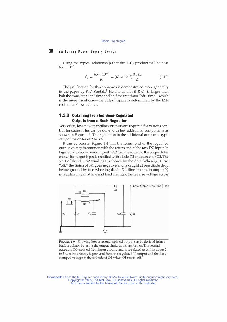
30 S w i t c h i n g P o w e r S u p p l y D e s i g n
Using the typical relationship that the RoCo product will be near65 × 10−6:
Co = 65 × 10−6
Ro= (65 × 10−6)
0.2Ion
Vor(1.10)
The justification for this approach is demonstrated more generallyin the paper by K.V. Kantak.1 He shows that if RoCo is larger thanhalf the transistor “on” time and half the transistor “off” time—whichis the more usual case—the output ripple is determined by the ESRresistor as shown above.
1.3.8 Obtaining Isolated Semi-RegulatedOutputs from a Buck Regulator
Very often, low-power ancillary outputs are required for various con-trol functions. This can be done with few additional components asshown in Figure 1.9. The regulation in the additional outputs is typi-cally of the order of 2 to 3%.
It can be seen in Figure 1.4 that the return end of the regulatedoutput voltage is common with the return end of the raw DC input. InFigure 1.9, a second winding with N2 turns is added to the output filterchoke. Its output is peak-rectified with diode D2 and capacitor C2. Thestart of the N1, N2 windings is shown by the dots. When Q1 turns“off,” the finish of N1 goes negative and is caught at one diode dropbelow ground by free-wheeling diode D1. Since the main output Vois regulated against line and load changes, the reverse voltage across
FIGURE 1.9 Showing how a second isolated output can be derived from abuck regulator by using the output choke as a transformer. The secondoutput is DC-isolated from input ground and is regulated to within about 2to 3%, as its primary is powered from the regulated Vo output and the fixedclamped voltage at the cathode of D1 when Q1 turns “off.”
Downloaded from Digital Engineering Library @ McGraw-Hill (www.digitalengineeringlibrary.com)Copyright © 2009 The McGraw-Hill Companies. All rights reserved.
Any use is subject to the Terms of Use as given at the website.
Basic Topologies
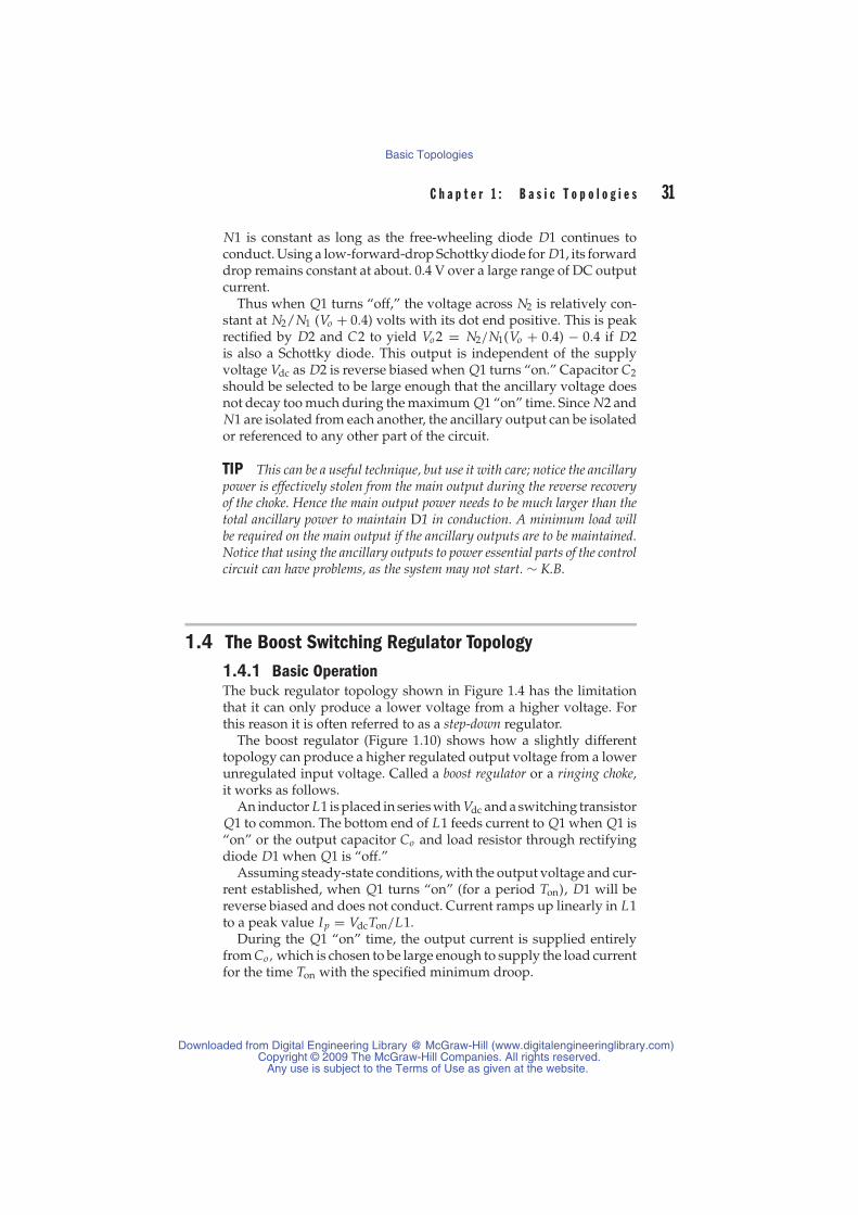
C h a p t e r 1 : B a s i c T o p o l o g i e s 31
N1 is constant as long as the free-wheeling diode D1 continues toconduct. Using a low-forward-drop Schottky diode for D1, its forwarddrop remains constant at about. 0.4 V over a large range of DC outputcurrent.
Thus when Q1 turns “off,” the voltage across N2 is relatively con-stant at N2/N1 (Vo + 0.4) volts with its dot end positive. This is peakrectified by D2 and C2 to yield Vo2 = N2/N1(Vo + 0.4) − 0.4 if D2is also a Schottky diode. This output is independent of the supplyvoltage Vdc as D2 is reverse biased when Q1 turns “on.” Capacitor C2should be selected to be large enough that the ancillary voltage doesnot decay too much during the maximum Q1 “on” time. Since N2 andN1 are isolated from each another, the ancillary output can be isolatedor referenced to any other part of the circuit.
TIP This can be a useful technique, but use it with care; notice the ancillarypower is effectively stolen from the main output during the reverse recoveryof the choke. Hence the main output power needs to be much larger than thetotal ancillary power to maintain D1 in conduction. A minimum load willbe required on the main output if the ancillary outputs are to be maintained.Notice that using the ancillary outputs to power essential parts of the controlcircuit can have problems, as the system may not start. ∼ K.B.
1.4 The Boost Switching Regulator Topology1.4.1 Basic OperationThe buck regulator topology shown in Figure 1.4 has the limitationthat it can only produce a lower voltage from a higher voltage. Forthis reason it is often referred to as a step-down regulator.
The boost regulator (Figure 1.10) shows how a slightly differenttopology can produce a higher regulated output voltage from a lowerunregulated input voltage. Called a boost regulator or a ringing choke,it works as follows.
An inductor L1 is placed in series with Vdc and a switching transistorQ1 to common. The bottom end of L1 feeds current to Q1 when Q1 is“on” or the output capacitor Co and load resistor through rectifyingdiode D1 when Q1 is “off.”
Assuming steady-state conditions, with the output voltage and cur-rent established, when Q1 turns “on” (for a period Ton), D1 will bereverse biased and does not conduct. Current ramps up linearly in L1to a peak value Ip = VdcTon/L1.
During the Q1 “on” time, the output current is supplied entirelyfrom Co, which is chosen to be large enough to supply the load currentfor the time Ton with the specified minimum droop.
Downloaded from Digital Engineering Library @ McGraw-Hill (www.digitalengineeringlibrary.com)Copyright © 2009 The McGraw-Hill Companies. All rights reserved.
Any use is subject to the Terms of Use as given at the website.
Basic Topologies
32 S w i t c h i n g P o w e r S u p p l y D e s i g n
FIGURE 1.10 Boost regulator and critical waveforms. Energy stored in L1during the Q1 “on” time is delivered to the output via D1 at a higher outputvoltage when Q1 turns “off” and the polarity across L1 reverses.
When Q1 turns “off,” since the current in an inductor cannot changeinstantaneously, the voltage across L1 reverses in an attempt to main-tain the current constant. Now the lower end of L1 goes positive withrespect to the input voltage. With the output voltage Vo higher thanthe input Vdc, L1 delivers its stored energy to Co via D1. Hence Cois boosted to a higher voltage than Vdc. This energy replenishes thecharge drained away from Co when D1 was not conducting. At thesame time current is also supplied to the load from Vdc via L1 and D1during this action.
In simple terms, the output voltage is regulated by controlling theQ1 “on” time in a negative-feedback loop. If the load current increases,
Downloaded from Digital Engineering Library @ McGraw-Hill (www.digitalengineeringlibrary.com)Copyright © 2009 The McGraw-Hill Companies. All rights reserved.
Any use is subject to the Terms of Use as given at the website.
Basic Topologies

C h a p t e r 1 : B a s i c T o p o l o g i e s 33
or the input voltage decreases, the “on” time of Q1 is automaticallyincreased to deliver more energy to the load, or the converse. Hence,in normal operation the “on” period of Q1 is adjusted to maintain theoutput voltage constant.
1.4.2 The Discontinuous Mode Actionin the Boost Regulator
TIP The boost regulator has two quite different modes of operation depend-ing on the conduction state of the inductor. If the inductor current reacheszero at the end of a cycle, it is said to operate in a discontinuous mode. Ifthere is some current remaining in the inductor at the end of a cycle, it is saidto be in a continuous mode of operation.
When speaking about switching regulators, the output filter capacitor isnot normally included in the analysis of the converter. The output currentof a switching regulator is, therefore, not the DC output current to the load,but rather the combined current that flows in the output capacitor and theload in parallel.
Notice that unlike the buck regulator, the boost regulator has a continuousinput current (with some ripple current) but a discontinuous output currentfor all modes of operation. Hence the terms continuous and discontinuousmode refer to what is going on in the inductor.
There is a dramatic difference in the transfer function between the twomodes of operation that significantly changes the transient performance andintrinsic stability. This is explained more fully in Chapter 12. ∼ K.B.
We will consider in more detail the action for discontinuous modeoperation, in which the energy in the inductor is completely trans-ferred to the output during the “off” period of Q1, and we will estab-lish some power and control equations.
We have seen that when Q1 turns “on,” the current ramps up lin-early in L1 to a peak value Ip = VdcTon/L1. Thus energy is stored inL1, and at the end of the “on” period, this stored energy will be
E = 0.5L1 I 2p (1.11)
where E is in joules, L is in henries, and Ip is in amperes.If the current through D1 (and hence L1) has fallen to zero before
the next Q1 turn “on” action, all the energy stored in L1 (Eq. 1.11)during the previous Q1 “on” period will have been delivered to theoutput load, and the circuit is said to be operating in the discontinuousmode.
The energy E in joules delivered to the load per cycle, divided bythe period T in seconds, is the output power in watts. Thus if all theenergy of Eq. 1.11 is delivered to the load once per period T, the power
Downloaded from Digital Engineering Library @ McGraw-Hill (www.digitalengineeringlibrary.com)Copyright © 2009 The McGraw-Hill Companies. All rights reserved.
Any use is subject to the Terms of Use as given at the website.
Basic Topologies

34 S w i t c h i n g P o w e r S u p p l y D e s i g n
to the load from L1 alone (assuming for the moment 100% efficiency)would be
PL =1/2L( Ip)2
T(1.12)
However, during the “off” time of Q1 (Tr in Figure 1.10d), the cur-rent in L1 is ramping down toward zero, and the same current is alsoflowing from the supply Vdc via L1 and D1 and is contributing tothe load power Pdc. This is equal to the average current during Trmultiplied by its duty cycle and Vdc as follows:
Pdc = VdcIp
2Tr
T(1.13)
The total power delivered to the load is then the sum of the twoparts as follows:
Pt = PL + Pdc =1/2L1( Ip)2
T+ Vdc
Ip
2Tr
T(1.14)
But Ip = VdcTon/L1. Substituting for Ip, in 1.14 we get
Pt = (1/2L1) (VdcTon/L1)2
T+ Vdc
VdcTon
2L1
Tr
T
= V2dcTon
2T L1(Ton + Tr ) (1.15)
To ensure that the current in L1 has ramped down to zero before thenext Q1 turn “on” action, we set (Ton + Tr ) to kT, where k is a fractionless than 1. (That is, the period T is made greater than the inductorconduction period.) Then
Pt = (V2
dcTon/2 TLl)(kT)
But for an output voltage Vo and output load resistor Ro,
Pt = V2dcTon
2T L1(kT) = V2
o
Ro
or
Vo = Vdc
√k Ro Ton
2L1(1.16)
Thus the negative-feedback loop keeps the output constant againstinput voltage changes and output load Ro changes in accordance withEq. 1.16. As Vdc and Ro (the load current) go down or up, the loop willincrease or decrease Ton so as to keep Vo constant.
Downloaded from Digital Engineering Library @ McGraw-Hill (www.digitalengineeringlibrary.com)Copyright © 2009 The McGraw-Hill Companies. All rights reserved.
Any use is subject to the Terms of Use as given at the website.
Basic Topologies
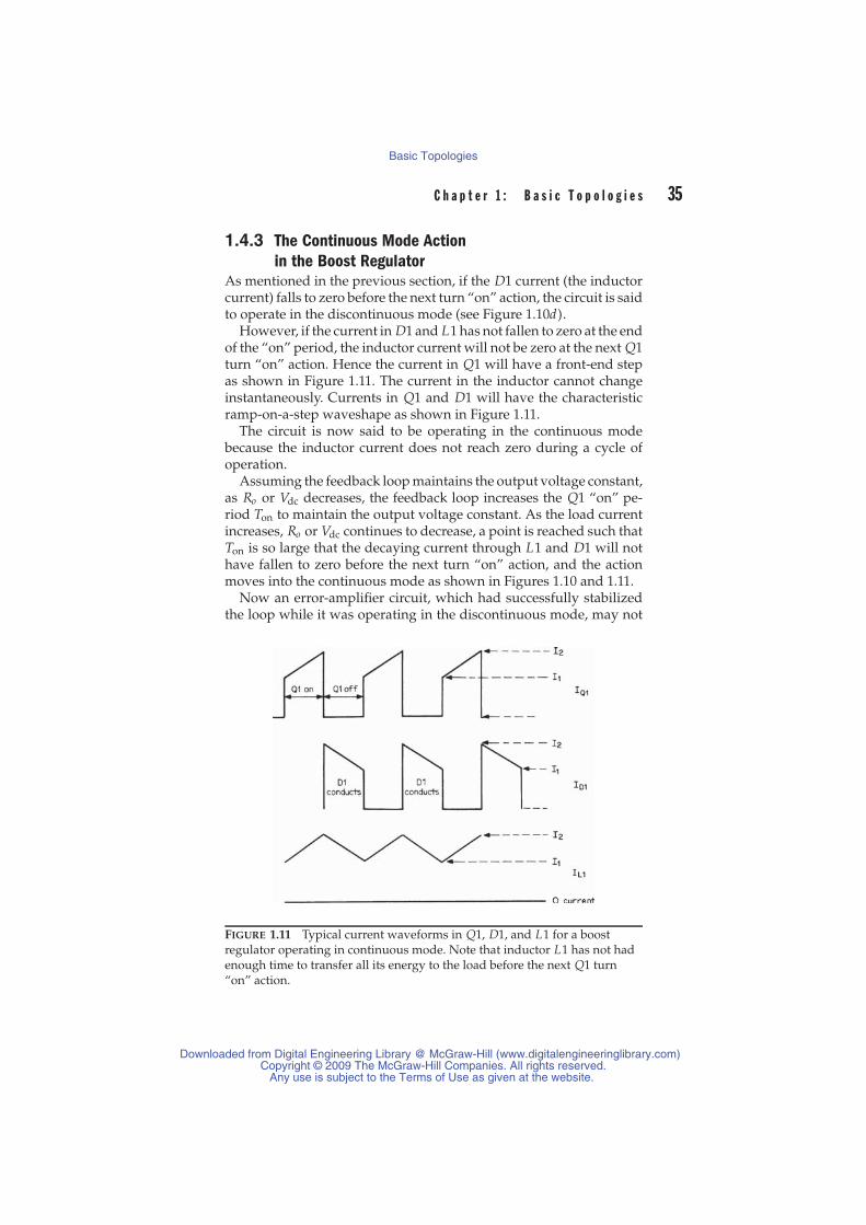
C h a p t e r 1 : B a s i c T o p o l o g i e s 35
1.4.3 The Continuous Mode Actionin the Boost Regulator
As mentioned in the previous section, if the D1 current (the inductorcurrent) falls to zero before the next turn “on” action, the circuit is saidto operate in the discontinuous mode (see Figure 1.10d).
However, if the current in D1 and L1 has not fallen to zero at the endof the “on” period, the inductor current will not be zero at the next Q1turn “on” action. Hence the current in Q1 will have a front-end stepas shown in Figure 1.11. The current in the inductor cannot changeinstantaneously. Currents in Q1 and D1 will have the characteristicramp-on-a-step waveshape as shown in Figure 1.11.
The circuit is now said to be operating in the continuous modebecause the inductor current does not reach zero during a cycle ofoperation.
Assuming the feedback loop maintains the output voltage constant,as Ro or Vdc decreases, the feedback loop increases the Q1 “on” pe-riod Ton to maintain the output voltage constant. As the load currentincreases, Ro or Vdc continues to decrease, a point is reached such thatTon is so large that the decaying current through L1 and D1 will nothave fallen to zero before the next turn “on” action, and the actionmoves into the continuous mode as shown in Figures 1.10 and 1.11.
Now an error-amplifier circuit, which had successfully stabilizedthe loop while it was operating in the discontinuous mode, may not
FIGURE 1.11 Typical current waveforms in Q1, D1, and L1 for a boostregulator operating in continuous mode. Note that inductor L1 has not hadenough time to transfer all its energy to the load before the next Q1 turn“on” action.
Downloaded from Digital Engineering Library @ McGraw-Hill (www.digitalengineeringlibrary.com)Copyright © 2009 The McGraw-Hill Companies. All rights reserved.
Any use is subject to the Terms of Use as given at the website.
Basic Topologies

36 S w i t c h i n g P o w e r S u p p l y D e s i g n
be able to keep the loop stable in the continuous mode and may oscil-late. In traditional feedback-loop analysis, the continuous-mode boostregulator has a right-half-plane-zero in the transfer function.2 The onlyway to stabilize a loop with a right-half-plane-zero is to drasticallyreduce the error-amplifier bandwidth.
TIP In simple terms, in the discontinuous mode, there is a short periodwhen there is zero current in the inductor and zero current in D1. That is,there is a small time-gap between the energy transfer period (when Q1 is“off” and D1 is conducting) and the energy storage period (when Q1 is “on”and D1 is not conducting). This time margin (dead time) is critical to theway the power system behaves and does not exist in the continuous mode.
It is very important to fully understand the difference between the twomodes of operation, because in any switching topology that has a boost-typebehavior, the effect will be evident. To better understand this, we will considera transient load increase in a continuous mode boost topology and follow thesequence of events as the circuit responds to the load change.
Consider a continuous-mode buck system, running in steady-state con-ditions, with a stabilized output voltage and a load current that maintainsthe inductor in continuous conduction. We now apply a sudden increase inload current. The output voltage will tend to fall, and the control loop willincrease the “on” period of Q1 to initiate an increase in current in L1. How-ever, it takes several cycles before the current in L1 will increase very much(depending on the value of the inductor, the input voltage, and the actualincrease in the Q1 “on” time).
It is important to notice that the immediate effect of increasing the “on”period is to decrease the “off” period (because the total period is fixed). SinceD1 only conducts during the “off” period of Q1 (and this period is immedi-ately reduced), the mean output current will initially decrease, rather thanincrease as was required. Hence we have a situation where we tried to increasethe output current, but the immediate effect was to reduce the output current.This will correct itself slowly as the current in the inductor increases over afew cycles.
From a control theory perspective, for a short time this effect introduces anadditional 180◦ of phase shift into the closed loop control system during thetransient period when the L1 current is increasing. In terms of control theorythis translates to a zero in the right half-plane of the transfer function; it isthe cause of the right-half-plane-zero in the small signal transfer function.
Notice that the effect is related to the dynamic behavior of the power compo-nents and cannot be changed by the control circuit. In fact, a perfect high-gainfast-response control circuit would result in the “on” period going to the fullpulse width on the first pulse, and there would be zero output current fora short period. Hence, the right-half-plane-zero cannot be eliminated by theloop compensation network. The only option is to slow down the rate ofchange of pulse width to allow the output to keep up without too much droop.
Downloaded from Digital Engineering Library @ McGraw-Hill (www.digitalengineeringlibrary.com)Copyright © 2009 The McGraw-Hill Companies. All rights reserved.
Any use is subject to the Terms of Use as given at the website.
Basic Topologies
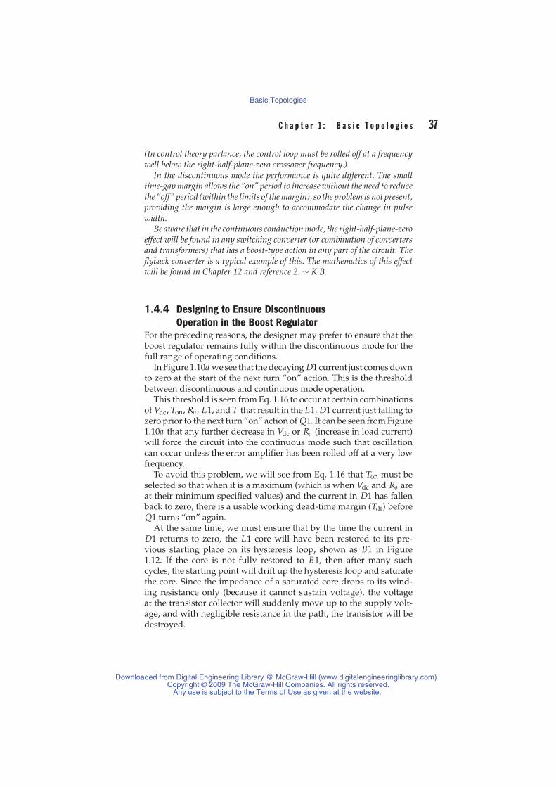
C h a p t e r 1 : B a s i c T o p o l o g i e s 37
(In control theory parlance, the control loop must be rolled off at a frequencywell below the right-half-plane-zero crossover frequency.)
In the discontinuous mode the performance is quite different. The smalltime-gap margin allows the “on” period to increase without the need to reducethe “off” period (within the limits of the margin), so the problem is not present,providing the margin is large enough to accommodate the change in pulsewidth.
Be aware that in the continuous conduction mode, the right-half-plane-zeroeffect will be found in any switching converter (or combination of convertersand transformers) that has a boost-type action in any part of the circuit. Theflyback converter is a typical example of this. The mathematics of this effectwill be found in Chapter 12 and reference 2. ∼ K.B.
1.4.4 Designing to Ensure DiscontinuousOperation in the Boost Regulator
For the preceding reasons, the designer may prefer to ensure that theboost regulator remains fully within the discontinuous mode for thefull range of operating conditions.
In Figure 1.10d we see that the decaying D1 current just comes downto zero at the start of the next turn “on” action. This is the thresholdbetween discontinuous and continuous mode operation.
This threshold is seen from Eq. 1.16 to occur at certain combinationsof Vdc, Ton, Ro, L1, and T that result in the L1, D1 current just falling tozero prior to the next turn “on” action of Q1. It can be seen from Figure1.10a that any further decrease in Vdc or Ro (increase in load current)will force the circuit into the continuous mode such that oscillationcan occur unless the error amplifier has been rolled off at a very lowfrequency.
To avoid this problem, we will see from Eq. 1.16 that Ton must beselected so that when it is a maximum (which is when Vdc and Ro areat their minimum specified values) and the current in D1 has fallenback to zero, there is a usable working dead-time margin (Tdt) beforeQ1 turns “on” again.
At the same time, we must ensure that by the time the current inD1 returns to zero, the L1 core will have been restored to its pre-vious starting place on its hysteresis loop, shown as B1 in Figure1.12. If the core is not fully restored to B1, then after many suchcycles, the starting point will drift up the hysteresis loop and saturatethe core. Since the impedance of a saturated core drops to its wind-ing resistance only (because it cannot sustain voltage), the voltageat the transistor collector will suddenly move up to the supply volt-age, and with negligible resistance in the path, the transistor will bedestroyed.
Downloaded from Digital Engineering Library @ McGraw-Hill (www.digitalengineeringlibrary.com)Copyright © 2009 The McGraw-Hill Companies. All rights reserved.
Any use is subject to the Terms of Use as given at the website.
Basic Topologies
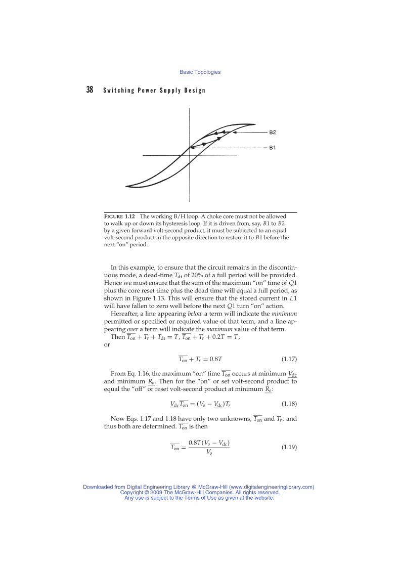
38 S w i t c h i n g P o w e r S u p p l y D e s i g n
FIGURE 1.12 The working B/H loop. A choke core must not be allowedto walk up or down its hysteresis loop. If it is driven from, say, B1 to B2by a given forward volt-second product, it must be subjected to an equalvolt-second product in the opposite direction to restore it to B1 before thenext “on” period.
In this example, to ensure that the circuit remains in the discontin-uous mode, a dead-time Tdt of 20% of a full period will be provided.Hence we must ensure that the sum of the maximum “on” time of Q1plus the core reset time plus the dead time will equal a full period, asshown in Figure 1.13. This will ensure that the stored current in L1will have fallen to zero well before the next Q1 turn “on” action.
Hereafter, a line appearing below a term will indicate the minimumpermitted or specified or required value of that term, and a line ap-pearing over a term will indicate the maximum value of that term.
Then Ton + Tr + Tdt = T , Ton + Tr + 0.2T = T ,or
Ton + Tr = 0.8T (1.17)
From Eq. 1.16, the maximum “on” time Ton occurs at minimum Vdcand minimum Ro . Then for the “on” or set volt-second product toequal the “off” or reset volt-second product at minimum Ro :
VdcTon = (Vo − Vdc)Tr (1.18)
Now Eqs. 1.17 and 1.18 have only two unknowns, Ton and Tr , andthus both are determined. Ton is then
Ton = 0.8T(Vo − Vdc)Vo
(1.19)
Downloaded from Digital Engineering Library @ McGraw-Hill (www.digitalengineeringlibrary.com)Copyright © 2009 The McGraw-Hill Companies. All rights reserved.
Any use is subject to the Terms of Use as given at the website.
Basic Topologies
C h a p t e r 1 : B a s i c T o p o l o g i e s 39
FIGURE 1.13 Boost regulator waveforms in the discontinuous mode with20% dead-time margin. For discontinuous-mode operation, the current in D1(see Figure 1.10) must have decayed to zero before the next turn “on” action.To ensure this, the inductor L1 is chosen such that Ton(max) + Tr = 0.8T ,leaving a dead time Tdt of 0.2T.
Now in Eq. 1.16, with Vdc and Ro (maximum load current) speci-fied, Ton is calculated from Eq. 1.19 and k[= (Ton + Tr )/T)] = 0.8 fromEq. 1.17.
Inductor L1 is fixed so the circuit is guaranteed not to enter thecontinuous mode. However, if the output load current is increasedbeyond its specified maximum value (Ro decreased below its speci-fied minimum) or Vdc is decreased below its specified minimum, thefeedback loop will attempt to increase Ton to keep Vo constant. Thiswill eat into the dead time, Tdt, and move the circuit closer to contin-uous mode. To avoid this, we must limit the maximum “on” time ora maximum peak current must be provided.
TIP A good method that accounts for all variables is to inhibit the turn “on”of Q1 until the inductor current reaches zero. For fixed-frequency operationthis limits the load current. Alternatively it can be set up to provide variable-frequency operation, which is often preferred. ∼ K.B.
Downloaded from Digital Engineering Library @ McGraw-Hill (www.digitalengineeringlibrary.com)Copyright © 2009 The McGraw-Hill Companies. All rights reserved.
Any use is subject to the Terms of Use as given at the website.
Basic Topologies

40 S w i t c h i n g P o w e r S u p p l y D e s i g n
With L1 determined earlier from Eq. 1.16, Vdc specified, and Toncalculated from Eq. 1.19, the peak current in Q1 can be calculatedfrom Eq. 1.14, and a transistor selected to have adequate gain at Ip .
The boost regulator is frequently used at low power levels in non-isolated applications due to the very low parts count. A typical appli-cation would be on a printed-circuit board where it is desired to stepup a 5-V computer logic level supply to, say, 12 or 15 V for operationalamplifiers.
Frequently at higher power levels in battery-supplied power sup-plies, as the battery discharges, its output voltage drops significantly.Many systems whose prime power is a nominal 12- or 28-V batterywill present problems when the battery voltage falls to about 9 or 22 V.Boost regulators are frequently used in such applications to boost thevoltages back up to the 12- and 28-V level. Power requirements in suchapplications can be in the range 50 to 200 watts.
1.4.5 The Link Between the Boost Regulatorand the Flyback Converter
The boost regulator has been treated in great detail because boostaction appears in many converter combinations. For example, by re-placing the inductor L1 with a transformer (more correctly a chokewith an additional secondary winding), a very similar, valuable, andwidely used topology, the flyback converter, is realized.
Like the boost, the flyback stores energy in its magnetics duringthe “on” period of the power device and transfers the energy to theoutput load during the “off” period.
Because the secondary windings can be isolated from the input,the outputs are not constrained to share a common return line. Alsoby using multiple secondaries, a multiple output power supply ispossible. The outputs may be higher or lower voltage than the input,and may be common or isolated as required.
The problems of discontinuous or continuous operation and thedesign relationships and procedures for the flyback are similar to thoseof the boost regulator and will be discussed in more detail in Chapter 4.
1.5 The Polarity Inverting Boost Regulator1.5.1 Basic OperationFigure 1.14 shows a different arrangement of the boost regulator thatprovides polarity inversion. It uses the same basic principle as theprevious boost regulator in that energy is stored in the inductor duringthe “on” period of Q1, which is then transferred to the output loadand Co in the “off” period of Q1.
Downloaded from Digital Engineering Library @ McGraw-Hill (www.digitalengineeringlibrary.com)Copyright © 2009 The McGraw-Hill Companies. All rights reserved.
Any use is subject to the Terms of Use as given at the website.
Basic Topologies
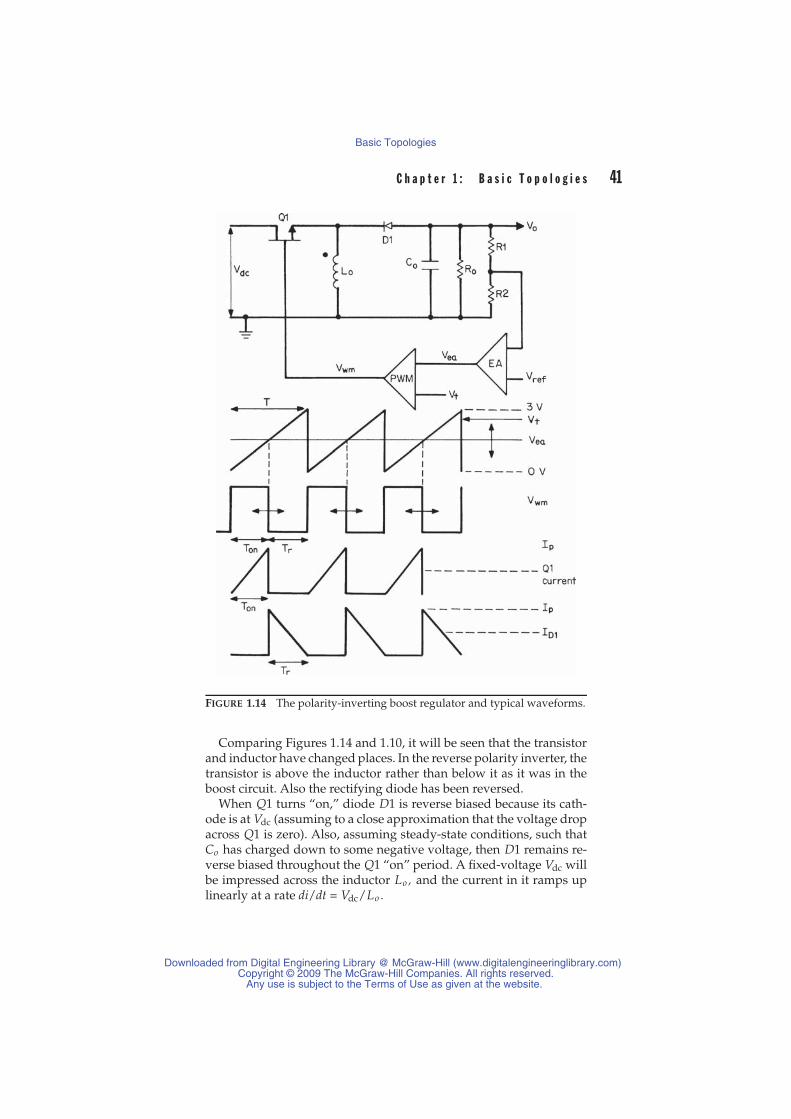
C h a p t e r 1 : B a s i c T o p o l o g i e s 41
FIGURE 1.14 The polarity-inverting boost regulator and typical waveforms.
Comparing Figures 1.14 and 1.10, it will be seen that the transistorand inductor have changed places. In the reverse polarity inverter, thetransistor is above the inductor rather than below it as it was in theboost circuit. Also the rectifying diode has been reversed.
When Q1 turns “on,” diode D1 is reverse biased because its cath-ode is at Vdc (assuming to a close approximation that the voltage dropacross Q1 is zero). Also, assuming steady-state conditions, such thatCo has charged down to some negative voltage, then D1 remains re-verse biased throughout the Q1 “on” period. A fixed-voltage Vdc willbe impressed across the inductor Lo, and the current in it ramps uplinearly at a rate di/dt = Vdc/Lo .
Downloaded from Digital Engineering Library @ McGraw-Hill (www.digitalengineeringlibrary.com)Copyright © 2009 The McGraw-Hill Companies. All rights reserved.
Any use is subject to the Terms of Use as given at the website.
Basic Topologies

42 S w i t c h i n g P o w e r S u p p l y D e s i g n
After an “on” period Ton, the current in Lo will have reached Ip =VdcTon/Lo, and the energy stored in Lo (in joules) is E = .5Lo I 2
p . WhenQ1 turns “off,” the voltage polarity across Lo reverses in an attemptto maintain its current constant. Thus at the instant of turn “off,” thesame inductor current Ip (which was flowing through Q1 before itturned “off”) now continues to flow down through Lo to common,pulling the current through D1 from Co . This current charges the topend of Co to a negative voltage.
After a number of cycles, when the required output voltage is de-veloped, the error amplifier adjusts the Q1 “on” period Ton so thatthe sampled output voltage Vo R2/(R1 + R2) is equal to the referencevoltage Vref. Further, if all the energy stored in Lo is delivered to theload before the next Q1 turn “on” action (that is, ID1 has fallen to zero),then the circuit operates in the discontinuous mode, and the powerdelivered to the load will be
Pt =1/2Lo I 2
p
T(1.20)
It should be noted that unlike the case of the boost regulator, whenQ1 turns “off,” the inductor current does not flow from the supplysource (see Eq. 1.13). Hence the only power to the load is that given byEq. 1.20. Thus assuming 100% efficiency, the output power would be
Po = V2o
Ro=
1/2Lo I 2p
T(1.21)
and for Ip = VdcTon/Lo,
Vo = VdcTon
√Ro
2T Lo(1.22)
1.5.2 Design Relations in the PolarityInverting Boost Regulator
As in the previous boost circuit, it is desirable to keep the circuit oper-ating in the discontinuous mode by ensuring that the current storedin Lo during the Q1 maximum “on” period has decayed to zero atthe end of the “off” period Tr . To ensure this action, we will providea dead time Tdt margin of 0.2T before the next Q1 turn “on” action.Thus if Ton + Tr + Tdt = T , then for Tdt = 0.2T we obtain
Ton + Tr = 0.8T (1.23)
In addition, as in the boost regulator, the “on” volt-second productmust equal the reset volt-second product to prevent the core from sat-urating. Since (as can be seen from Eq. 1.22) the maximum Ton occurs
Downloaded from Digital Engineering Library @ McGraw-Hill (www.digitalengineeringlibrary.com)Copyright © 2009 The McGraw-Hill Companies. All rights reserved.
Any use is subject to the Terms of Use as given at the website.
Basic Topologies

C h a p t e r 1 : B a s i c T o p o l o g i e s 43
for minimum Vdc and minimum Ro (maximum current), it followsthat
VdcTon = Vo Tr (1.24)
Thus both Eqs. 1.23 and 1.24 have two unknowns: Ton and Tr . Thisfixes Ton at
Ton = 0.8Vo TVdc + Vo
(1.25)
Now, with Ton calculated from Eq. 1.25 and Vdc, Ro ,Vo , and T spec-ified, Eq. 1.22 defines Lo such that Ip = VdcTon/Lo, and transistor Q1is selected to have adequate gain at Ip .
References1. K. V. Kantak, “Output Voltage Ripple in Switching Power Converters,” in Power
Electronics Conference Proceedings, Boxborough, MA, pp. 35–44, April 1987.2. K. Billings, Switchmode Power Supply Handbook, New York: McGraw-Hill, 1999,
Chap. 9.
Downloaded from Digital Engineering Library @ McGraw-Hill (www.digitalengineeringlibrary.com)Copyright © 2009 The McGraw-Hill Companies. All rights reserved.
Any use is subject to the Terms of Use as given at the website.
Basic Topologies

Downloaded from Digital Engineering Library @ McGraw-Hill (www.digitalengineeringlibrary.com)Copyright © 2009 The McGraw-Hill Companies. All rights reserved.
Any use is subject to the Terms of Use as given at the website.
Basic Topologies
C H A P T E R 2Push-Pull and ForwardConverter Topologies
2.1 IntroductionIn the three switching regulator topologies discussed in the previouschapter, the output returns were all common with the input returns,and multiple outputs were not possible (except for the special casediscussed in Section 1.3.8).
In this chapter we look at some of the most widely used fullyisolated switching regulator topologies. These topologies—the push-pull, single-ended forward converter, and the double-ended and inter-leaved forward converters—are similar, so we consider them a singlefamily. All these topologies deliver their power to the loads via a high-frequency transformer; hence outputs may be DC-isolated from theinput, and multiple outputs are possible.
2.2 The Push-Pull Topology2.2.1 Basic Operation (With Master/
Slave Outputs)A push-pull topology is shown in Figure 2.1. It consists of a trans-former T1 with multiple secondaries. Each secondary delivers a pairof 180◦ out-of-phase square-wave power pulses whose amplitude isfixed by the input voltage and the number of primary and secondaryturns.
The pulse widths for all secondaries are identical, as determined bythe control circuit and the negative-feedback loop around the masteroutput. The control circuit is similar to the buck and boost regula-tors shown previously in Figures 1.4 and 1.10, except that two equal
45Downloaded from Digital Engineering Library @ McGraw-Hill (www.digitalengineeringlibrary.com)
Copyright © 2009 The McGraw-Hill Companies. All rights reserved.Any use is subject to the Terms of Use as given at the website.
Source: Switching Power Supply Design
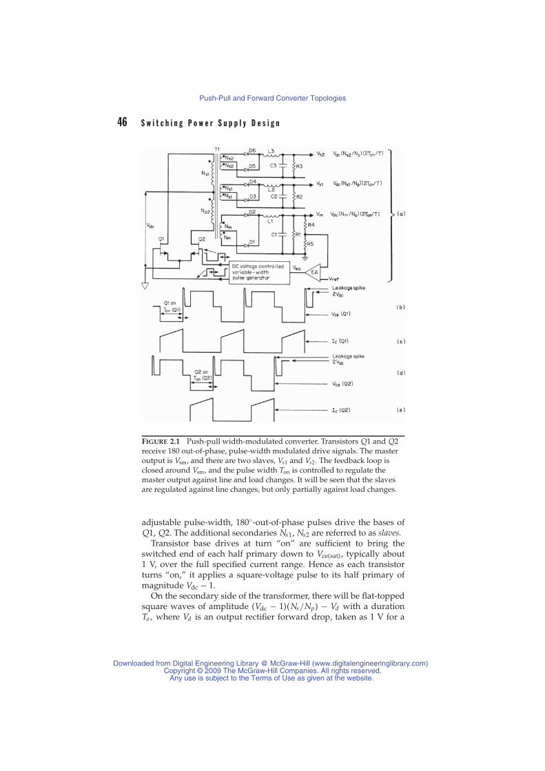
46 S w i t c h i n g P o w e r S u p p l y D e s i g n
FIGURE 2.1 Push-pull width-modulated converter. Transistors Q1 and Q2receive 180 out-of-phase, pulse-width modulated drive signals. The masteroutput is Vsm, and there are two slaves, Vs1 and Vs2. The feedback loop isclosed around Vsm, and the pulse width Ton is controlled to regulate themaster output against line and load changes. It will be seen that the slavesare regulated against line changes, but only partially against load changes.
adjustable pulse-width, 180◦-out-of-phase pulses drive the bases ofQ1, Q2. The additional secondaries Ns1, Ns2 are referred to as slaves.
Transistor base drives at turn “on” are sufficient to bring theswitched end of each half primary down to Vce(sat) , typically about1 V, over the full specified current range. Hence as each transistorturns “on,” it applies a square-voltage pulse to its half primary ofmagnitude Vdc − 1.
On the secondary side of the transformer, there will be flat-toppedsquare waves of amplitude (Vdc − 1)(Ns/Np) − Vd with a durationTo, where Vd is an output rectifier forward drop, taken as 1 V for a
Downloaded from Digital Engineering Library @ McGraw-Hill (www.digitalengineeringlibrary.com)Copyright © 2009 The McGraw-Hill Companies. All rights reserved.
Any use is subject to the Terms of Use as given at the website.
Push-Pull and Forward Converter Topologies
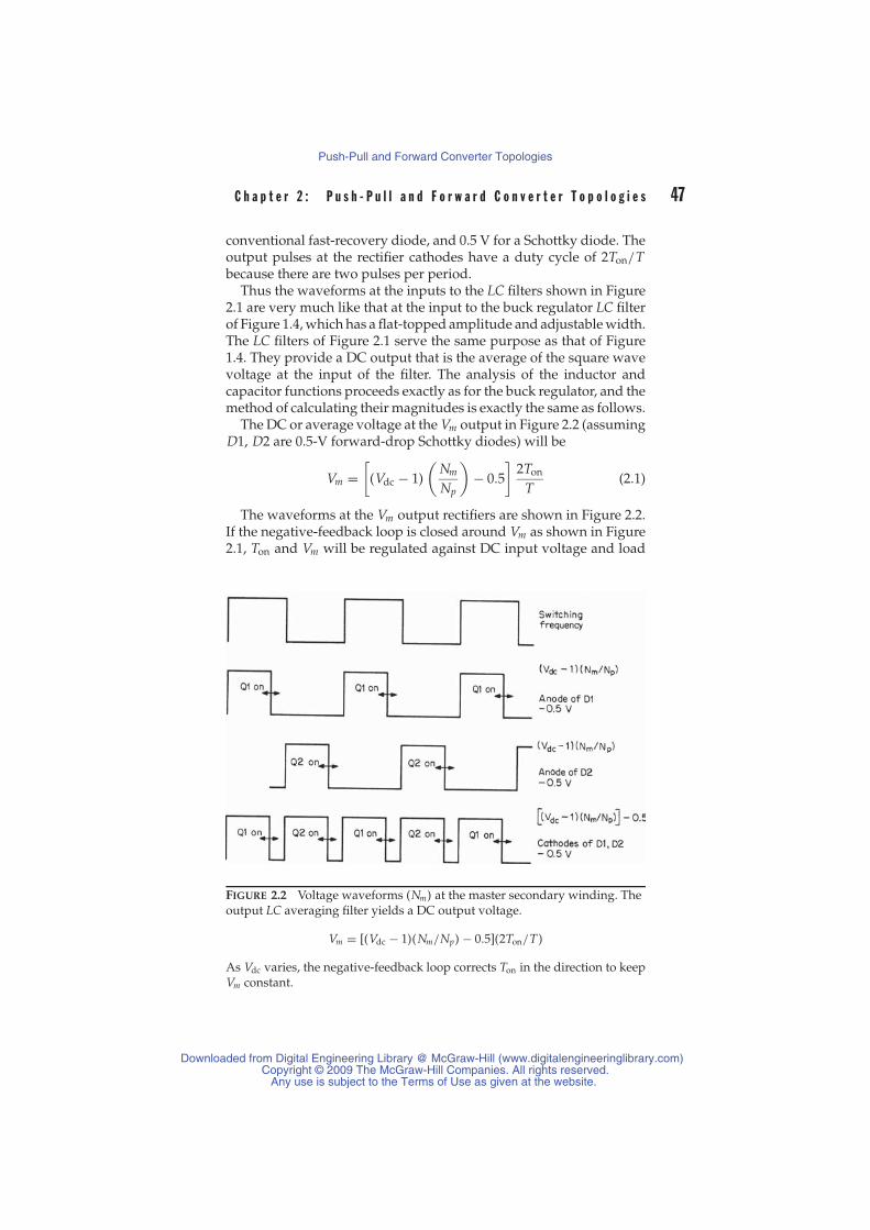
C h a p t e r 2 : P u s h - P u l l a n d F o r w a r d C o n v e r t e r T o p o l o g i e s 47
conventional fast-recovery diode, and 0.5 V for a Schottky diode. Theoutput pulses at the rectifier cathodes have a duty cycle of 2Ton/Tbecause there are two pulses per period.
Thus the waveforms at the inputs to the LC filters shown in Figure2.1 are very much like that at the input to the buck regulator LC filterof Figure 1.4, which has a flat-topped amplitude and adjustable width.The LC filters of Figure 2.1 serve the same purpose as that of Figure1.4. They provide a DC output that is the average of the square wavevoltage at the input of the filter. The analysis of the inductor andcapacitor functions proceeds exactly as for the buck regulator, and themethod of calculating their magnitudes is exactly the same as follows.
The DC or average voltage at the Vm output in Figure 2.2 (assumingD1, D2 are 0.5-V forward-drop Schottky diodes) will be
Vm =[
(Vdc − 1)(
Nm
Np
)− 0.5
]2Ton
T(2.1)
The waveforms at the Vm output rectifiers are shown in Figure 2.2.If the negative-feedback loop is closed around Vm as shown in Figure2.1, Ton and Vm will be regulated against DC input voltage and load
FIGURE 2.2 Voltage waveforms (Nm) at the master secondary winding. Theoutput LC averaging filter yields a DC output voltage.
Vm = [(Vdc − 1)(Nm/Np) − 0.5](2Ton/T)
As Vdc varies, the negative-feedback loop corrects Ton in the direction to keepVm constant.
Downloaded from Digital Engineering Library @ McGraw-Hill (www.digitalengineeringlibrary.com)Copyright © 2009 The McGraw-Hill Companies. All rights reserved.
Any use is subject to the Terms of Use as given at the website.
Push-Pull and Forward Converter Topologies
48 S w i t c h i n g P o w e r S u p p l y D e s i g n
current changes. Although load current does not appear in Eq. 2.1, acurrent change will cause Vm to change, that change will be sensed bythe error amplifier, and Ton will be altered to correct it. Providing thecurrent in L1 (see Figure 2.1) does not go discontinuous, changes inTon will be small, and the absolute value of Ton will be given by Eq. 2.1for any turns ratio Nm/Np,input voltageVdc, and period T.
For the slave secondaries, the voltages at the cathodes of the rec-tifying diodes are fixed by the number of secondary turns, and theTon duration of the square waves is the same as defined by the masterfeedback loop. Thus the slave output voltages with normal diodeswill be
Vs1 =[
(Vdc − 1)Ns1
Np− 1
]2Ton
T(2.2)
Vs2 =[
(Vdc − 1)Ns2
Np− 1
]2Ton
T(2.3)
2.2.2 Slave Line-Load RegulationIt can be seen from Eqs. 2.1, 2.2, and 2.3 that the slaves are regulatedagainst Vdc input changes by the negative-feedback loop that keepsVm constant, in accordance with Eq. 2.1. The same equation,
Vm = (Vdc − 1)Ton
also appears in Eqs. 2.2 and 2.3, and thus Vs1, Vs2 are also kept constantas Vdc changes.
Notice that if load current in the master (Vm) changes, the dropsacross its rectifying diodes and winding resistance will change slightly.Thus the negative-feedback loop will correct for Vm load change effectsand alter Ton to keep Vm constant.
For the slave outputs, Ton will now change without correspondingchanges in Vdc, and from Eqs. 2.2 and 2.3, it can be seen that changesin Vs1, Vs2 will result. Such changes in the slave output voltages due tochanges in the master output current are referred to as cross regulation.
Slave output voltages will also change as a result of changes intheir own output currents. In a similar way slave current changes willcause voltage drop changes in their rectifying diodes and windingresistances, lowering the peak voltages slightly. These changes arenot corrected by the main feedback loop, which senses only Vm.
However, providing the currents in the slave output inductors L2,L3, and especially in the master inductor L1 do not go discontinuous,slave output voltages can be depended on to vary within only ± 5 to± 8%.
Downloaded from Digital Engineering Library @ McGraw-Hill (www.digitalengineeringlibrary.com)Copyright © 2009 The McGraw-Hill Companies. All rights reserved.
Any use is subject to the Terms of Use as given at the website.
Push-Pull and Forward Converter Topologies

C h a p t e r 2 : P u s h - P u l l a n d F o r w a r d C o n v e r t e r T o p o l o g i e s 49
TIP Much better cross regulation can be obtained by using coupled outputinductors (where all outputs share a common inductor core).1∼ K.B.
2.2.3 Slave Output Voltage ToleranceAlthough changes in slave output voltages are relatively small, theabsolute values of output voltage are not accurately adjustable. Asseen in Eqs. 2.2 and 2.3, they are fixed by Ton and their correspondingsecondary turns Ns1, Ns2. But Ton is nearly constant, defined by thefeedback loop to keep the master voltage constant. Further, since theturns can be changed only by integral numbers, the absolute value ofslave output voltage is not finely settable. The change in secondaryvoltage for a single turn change in Ns is given by Vm. Ton/Np .
In most cases, the absolute values of slave output voltage are not tooimportant. Slaves usually drive operational amplifiers or motors, andmost often these can tolerate DC voltages within about 2 V of a desiredvalue. If the absolute magnitude is important, the output voltage isusually designed to be higher than required and brought down to adesired exact value with a linear or buck regulator. Because a slaveoutput is semi-regulated, a linear regulator is reasonably efficient.
2.2.4 Master Output Inductor MinimumCurrent Limitations
The selection of the output inductor for a buck regulator was dis-cussed in Section 1.3.6. It was mentioned that at the average currentin which the step at the front of the inductor current waveform hasfallen to zero (see Figures 1.6a and 1.6b), the inductor is said to run dryor to go discontinuous. Below this average current, the feedback loopmaintains the buck regulator’s output voltage constant by reducingthe “on” period; this results in reduction of slave output voltages.
In Figure 1.6a, however, it can be seen that at currents above goingdiscontinuous, the “on” time is very nearly constant over large outputcurrent changes. Below run-dry, the “on” time changes drastically.In the buck regulator this does not pose a major problem becauseonly one output is involved and the feedback loop keeps this outputvoltage constant. But in the push-pull width-modulated converterwith a master and some slaves, the slave output voltages are directlyproportional to the master “on” time, as shown by Eqs. 2.2 and 2.3.
Hence, when slaves are involved it is important that the averagemaster output inductor current not be permitted to go discontinuousabove its specified minimum. If the master minimum output currentis specified at one-tenth its nominal value for example, a minimumoutput inductor value must be selected from Eq. 1.8. The slave out-put voltages will vary within about 5% above the master inductor
Downloaded from Digital Engineering Library @ McGraw-Hill (www.digitalengineeringlibrary.com)Copyright © 2009 The McGraw-Hill Companies. All rights reserved.
Any use is subject to the Terms of Use as given at the website.
Push-Pull and Forward Converter Topologies

50 S w i t c h i n g P o w e r S u p p l y D e s i g n
discontinuous current. Below this critical current, the feedback loopwill keep the master output voltage constant by decreasing Ton signif-icantly, followed by the slave output voltages.
Further, the slave outputs must not be permitted to go discontin-uous above their own specified minimum currents. Slave output in-ductors should also be selected from Eq. 1.8. Clearly, larger minimumcurrents imply smaller inductors.
TIP This problem is also eliminated by using coupled output inductors.1
∼ K.B.
The push-pull converter is one of the oldest topologies and isstill popular. It can provide multiple outputs whose returns areDC-isolated from input ground and from one another. Output volt-ages can be higher or lower than the input voltage. The master isregulated against line and load variations. The slaves are equallywell regulated against line changes and can be within about 5% forload changes as long as output inductors are not permitted to godiscontinuous.
2.2.5 Flux Imbalance in the Push-PullTopology (Staircase Saturation Effects)
The designer needs to be aware of a rather subtle failure mode in push-pull converters, known as staircase saturation, caused by a possible fluximbalance in the transformer core.
This effect can best be understood by examination of a typical hys-teresis loop of a ferrite core material used in the power transformer asshown in Figure 2.3.
In normal operation, core flux excursions are between levels suchas B1 and B2 gauss in Figure 2.3. It is important to stay on the linearpart of the hysteresis loop below about ± 2000 G. At frequencies upto 25 kHz or so, core losses are low and these maximum excursionsare permissible. As discussed in Section 2.2.9.4, however, core lossesgo up rapidly with frequency, and above 100 kHz conservative designlimits peak flux density to 1200 or even 800 G.
It can be seen in Figure 2.1 that when Q1 is “on,” the no-dot end ofNp1 is positive with respect to the dot end, and the core moves up thehysteresis loop—say, from B1 toward B2. The actual amount it movesup is proportional to the product of the voltage across Np1 and Q1“on” time (from Faraday’s law; see Eq. 1.18). When Q1 turns “off”and Q2 turns “on,” the dot end of Np2 is positive with respect to theno-dot end, and the core moves back down from B2 toward B1. Theactual amount it moves down is proportional to the voltage acrossNp2 and the Q2 “on” time.
Downloaded from Digital Engineering Library @ McGraw-Hill (www.digitalengineeringlibrary.com)Copyright © 2009 The McGraw-Hill Companies. All rights reserved.
Any use is subject to the Terms of Use as given at the website.
Push-Pull and Forward Converter Topologies
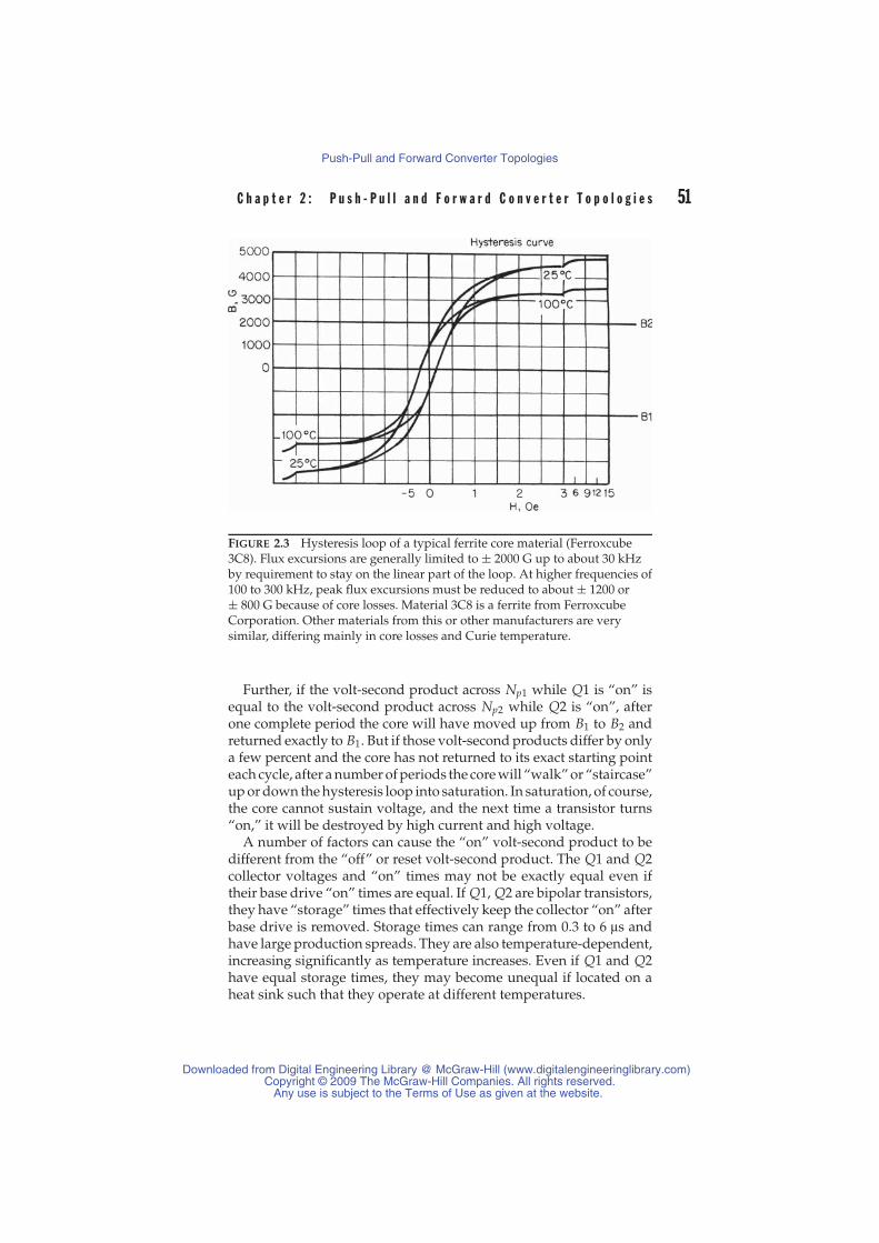
C h a p t e r 2 : P u s h - P u l l a n d F o r w a r d C o n v e r t e r T o p o l o g i e s 51
FIGURE 2.3 Hysteresis loop of a typical ferrite core material (Ferroxcube3C8). Flux excursions are generally limited to ± 2000 G up to about 30 kHzby requirement to stay on the linear part of the loop. At higher frequencies of100 to 300 kHz, peak flux excursions must be reduced to about ± 1200 or± 800 G because of core losses. Material 3C8 is a ferrite from FerroxcubeCorporation. Other materials from this or other manufacturers are verysimilar, differing mainly in core losses and Curie temperature.
Further, if the volt-second product across Np1 while Q1 is “on” isequal to the volt-second product across Np2 while Q2 is “on”, afterone complete period the core will have moved up from B1 to B2 andreturned exactly to B1. But if those volt-second products differ by onlya few percent and the core has not returned to its exact starting pointeach cycle, after a number of periods the core will “walk” or “staircase”up or down the hysteresis loop into saturation. In saturation, of course,the core cannot sustain voltage, and the next time a transistor turns“on,” it will be destroyed by high current and high voltage.
A number of factors can cause the “on” volt-second product to bedifferent from the “off” or reset volt-second product. The Q1 and Q2collector voltages and “on” times may not be exactly equal even iftheir base drive “on” times are equal. If Q1, Q2 are bipolar transistors,they have “storage” times that effectively keep the collector “on” afterbase drive is removed. Storage times can range from 0.3 to 6 μs andhave large production spreads. They are also temperature-dependent,increasing significantly as temperature increases. Even if Q1 and Q2have equal storage times, they may become unequal if located on aheat sink such that they operate at different temperatures.
Downloaded from Digital Engineering Library @ McGraw-Hill (www.digitalengineeringlibrary.com)Copyright © 2009 The McGraw-Hill Companies. All rights reserved.
Any use is subject to the Terms of Use as given at the website.
Push-Pull and Forward Converter Topologies

52 S w i t c h i n g P o w e r S u p p l y D e s i g n
Hence if one transistor has a volt-second product only slightly largerthan the other, it will start the core progressively drifting off-centertoward saturation with each cycle. This will cause one transistor todraw slightly more current than the other as the core moves onto thecurved part of the hysteresis loop (see Figure 2.3). As a result, the coremagnetizing current on that half-period starts to become a significantpart of the load current. The transistor that draws more current willnow run slightly warmer, increasing its storage time. With a longerstorage time in that transistor, the volt-second product it applies to thecore in its “on” half period increases, the current in that half periodincreases, and storage time in that transistor increases still further.Thus a runaway condition arises that quickly drives the core intosaturation and destroys the transistor.
The “on” volt-second products of Q1 and Q2 also can differ becauseof their initially unequal “on” or Vce(sat) voltages, which have a signifi-cant production spread. As described earlier, with bipolar transistors,any initial difference in “on” voltage is magnified because the “on”voltage of bipolars decreases as temperature increases.
If Q1, Q2 are MOSFETs (Metal-Oxide-Semiconductor Field-EffectTransistors), the flux-imbalance problem is much less serious. To startwith, MOSFETs have no storage time, and with equal input “on” (gate)times, output (drain) times are equal and, importantly, the “on” volt-age of a MOSFET transistor increases as temperature increases. Thusthe runaway condition described earlier is reversed, providing somecompensation. If there were any initial volt-second inequality, one FETcurrent would be greater as the core started moving up the curvedpart of the hysteresis loop. The FET with the larger current would runwarmer, and its “on” voltage would increase and rob voltage from itshalf primary. This would decrease the volt-second product in that half-period and bring the transistor current back down, providing somecompensation.
2.2.6 Indications of Flux ImbalanceThe earlier description might imply that any slight imbalance in volt-second product between half cycles causes certain failure, but thisis not necessarily so. A push-pull converter can continue to operatereliably with a small amount of flux imbalance without immediatelysaturating its core and destroying its transistors. Many low power,low voltage push-pull converter designs run quite reliably in spite ofthe apparent problems.
Notice that with a small volt-second imbalance, if there were notan inherent corrective mechanism, core saturation and transistor fail-ure would always occur after a few switching cycles. Thus, if therewere an initial volt-second imbalance of say 0.01% (which would be
Downloaded from Digital Engineering Library @ McGraw-Hill (www.digitalengineeringlibrary.com)Copyright © 2009 The McGraw-Hill Companies. All rights reserved.
Any use is subject to the Terms of Use as given at the website.
Push-Pull and Forward Converter Topologies

C h a p t e r 2 : P u s h - P u l l a n d F o r w a r d C o n v e r t e r T o p o l o g i e s 53
practically impossible to achieve), it would take only 10,000 cyclesuntil the core would move from a low starting point of B1 (see Figure2.3) to a saturating point of B2, and the transistors would probably bedestroyed before that.
One corrective mechanism, that may permit the converter to sur-vive, is the primary winding resistance. If there is an initial volt-secondimbalance, the transistor taking more current produces a larger volt-age drop across its half primary winding resistance. That voltage droprobs volt-seconds from the winding and tends to restore the volt-second balance.
Thus the converter can remain in an unbalanced state without im-mediately going into runaway and completely saturating the core. Anindication of where the core is working on the hysteresis loop can beobtained by placing a current probe in the transformer center tap asshown in Figure 2.4d.
The waveform indicating volt-second balance is shown in Figure2.4a, where alternate current peaks are equal. Primary load currentpulses have the characteristic shape of a ramp on a step just as for thebuck regulator in Figure 1.4d. They have this shape because all thesecondaries have output LC filters that generate such waveshapes asdescribed in Section 1.3.2.
The primary load current is the sum of all the secondary currentsreflected into the primary by their respective turn ratios. However,the total primary current is the sum of these secondary currents plusthe primary magnetizing current. The magnetizing current is the cur-rent drawn by the magnetizing inductance, which is the inductanceseen looking into the primary with all secondaries open-circuited.This inductance is always present and effectively is in parallel withthe primary winding. This current is added to the secondary currentsreflected into the primary as in Figure 2.4e.
The waveshape of the total primary current is then the sum of theramp-on-a-step reflected load currents and the magnetizing current.But providing the core is working in the linear area of the B/H loop, themagnetizing current will be a linear ramp starting from zero currenteach cycle.
When a transistor turns “on,” it applies a step of voltage of approx-imately Vdc − 1 across the magnetizing inductance L pm. Magnetizingcurrent then ramps up linearly at a rate
dI/dt = (Vdc − 1)/L pm (2.4)
and for the transistor “on” time of Ton it reaches a peak of
Ipm = (Vdc − 1)(Ton)L pm
(2.5)
Downloaded from Digital Engineering Library @ McGraw-Hill (www.digitalengineeringlibrary.com)Copyright © 2009 The McGraw-Hill Companies. All rights reserved.
Any use is subject to the Terms of Use as given at the website.
Push-Pull and Forward Converter Topologies
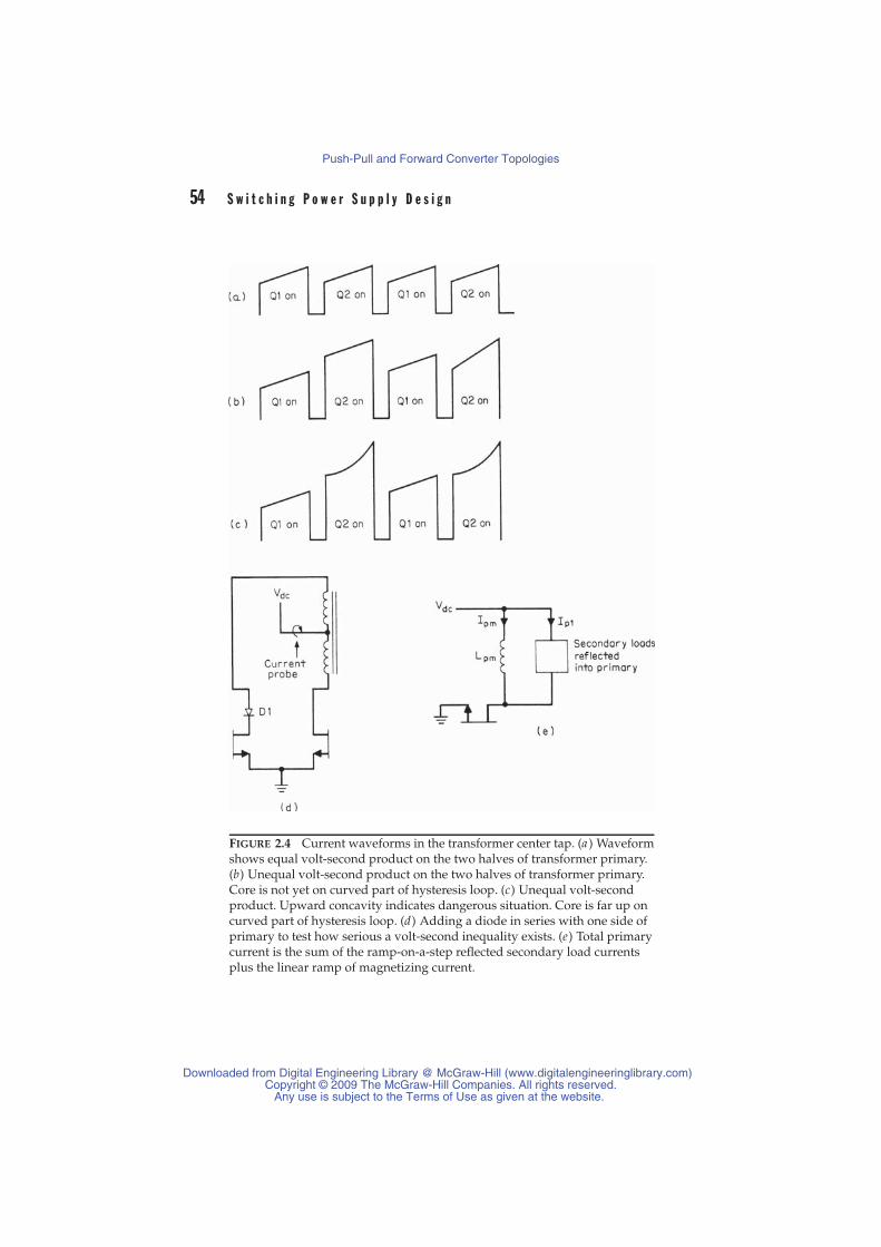
54 S w i t c h i n g P o w e r S u p p l y D e s i g n
FIGURE 2.4 Current waveforms in the transformer center tap. (a ) Waveformshows equal volt-second product on the two halves of transformer primary.(b) Unequal volt-second product on the two halves of transformer primary.Core is not yet on curved part of hysteresis loop. (c) Unequal volt-secondproduct. Upward concavity indicates dangerous situation. Core is far up oncurved part of hysteresis loop. (d) Adding a diode in series with one side ofprimary to test how serious a volt-second inequality exists. (e) Total primarycurrent is the sum of the ramp-on-a-step reflected secondary load currentsplus the linear ramp of magnetizing current.
Downloaded from Digital Engineering Library @ McGraw-Hill (www.digitalengineeringlibrary.com)Copyright © 2009 The McGraw-Hill Companies. All rights reserved.
Any use is subject to the Terms of Use as given at the website.
Push-Pull and Forward Converter Topologies

C h a p t e r 2 : P u s h - P u l l a n d F o r w a r d C o n v e r t e r T o p o l o g i e s 55
The magnetizing current Ipm is kept small compared with the sum ofthe load currents reflected into the primary by ensuring that L pm inEq. 2.5 is large. By design, the peak magnetizing current should be nogreater than 10% of the primary load current.
When added to the ramp-on-a-step load current, the ramp of mag-netizing current is small, and it simply increases the slope of the latterslightly. Also, if the volt-seconds are equal on alternate half cycles, thepeak currents will also be equal on each half cycle as in Figure 2.4a,because operation is centered around the origin of the hysteresis loopof Figure 2.3.
However, if the volt-second products on alternate half cycles areunequal, core operation is not centered on the origin of the hysteresisloop. Since the horizontal scale (H oersteds) is proportional to mag-netizing current, this shows up as a DC current bias as in Figure 2.4b,making alternate current pulses unequal in amplitude.
As long as the DC bias does not drive the core up the hysteresisloop appreciably, the slope of the ramp still remains linear (Fig. 2.4b)and operation is still reasonably safe. Primary wiring resistance maykeep the core from moving further up into saturation.
But if there is a large inequality in volt-seconds on alternate halfcycles, the core is biased closer toward saturation and enters thecurved part of the hysteresis loop. Now the magnetizing inductance,which is proportional to the slope of the hysteresis loop, decreasesand magnetizing current increases significantly. This shows up as anupward concavity in the current slope in Figure 2.4c.
This is a dangerous and imminent failure situation. Now even asmall temperature increase can bring on the runaway scenario de-scribed earlier. The core will be driven hard into saturation and destroythe power transistor. A push-pull converter design should certainlynot be considered safe if current pulses in the primary center tap showany upward concavity in their ramps. Even linear ramps as in Figure2.4b with anything greater than 20% inequality in peak currents areunsafe and should not be accepted.
Note A more damaging effect can occur if there is a sudden transientload change, because the extra current can take the core immediately intosaturation. ∼ K.B.
2.2.7 Testing for Flux ImbalanceA simple test to determine how close to a dangerous flux-imbalancesituation a push-pull converter may be operating is shown in Figure2.4d. Here a silicon diode with about 1 V forward drop is placedin series with one half of the transformer primary. Now in the “on”state, that half with the diode in series has 1 V less voltage across it
Downloaded from Digital Engineering Library @ McGraw-Hill (www.digitalengineeringlibrary.com)Copyright © 2009 The McGraw-Hill Companies. All rights reserved.
Any use is subject to the Terms of Use as given at the website.
Push-Pull and Forward Converter Topologies

56 S w i t c h i n g P o w e r S u p p l y D e s i g n
than the other half, and there is an artificially produced volt-secondunbalance. The center tap waveform will then look like either Figure2.4b or 2.4c. The current ramp corresponding to the side that does nothave the diode will have the larger volt-second product and the largerpeak current. By switching the diode to the other side, the larger peakcurrent will be seen to switch to the opposite transformer half primary.
Now the closeness of the circuit to the upward concave situation ofFigure 2.4c can be determined. If one series diode can make a currentramp go concave, the circuit is too close to imminent failure. Placingtwo series diodes on one side will give an indication of how muchmargin there is.
It should be noted that primary magnetizing current contributesno power to the secondaries. It will not appear in the secondaries. Itsimply swings the magnetic core across the hysteresis loop.
In Figure 2.3, the magnetizing force H in oersteds (Oe) is related tothe current by the fundamental magnetic relation
H = 0.4π Np Im
lm(2.6)
where Np is the number of primary turnsIm is the magnetizing current in ampereslm is the magnetic path length in cm
2.2.8 Coping with Flux ImbalanceFlux imbalance can become a major problem at high voltages and highpowers. There are a number of ways to circumvent the problem, butmost involve increased cost or component count. Some schemes tocombat flux imbalance are described in the following subsections.
2.2.8.1 Gapping the CoreFlux imbalance becomes serious when the core moves out onto thecurved part of the hysteresis loop (see Figure 2.3) and magnetizingcurrent starts increasing exponentially as in Figure 2.4c. This effectcan be reduced by moving the curved part of the hysteresis loop to ahigher current by tilting the hysteresis loop. The core can then toleratea larger DC current bias or volt-second product inequality.
An air gap introduced into the magnetic path of the core has theeffect shown in Figure 2.5. It tilts the slope of the hysteresis loop.An air gap of 2 to 4 mils (thousandths of an inch) brings the curvedportion of the loop much further away from the origin so that the corecan accept a reasonably large offset in H (current imbalance). Thiscan help at higher power levels. It has the disadvantage of reducingthe inductance so that the critical current must be larger to preventdiscontinuous-mode operation.
Downloaded from Digital Engineering Library @ McGraw-Hill (www.digitalengineeringlibrary.com)Copyright © 2009 The McGraw-Hill Companies. All rights reserved.
Any use is subject to the Terms of Use as given at the website.
Push-Pull and Forward Converter Topologies
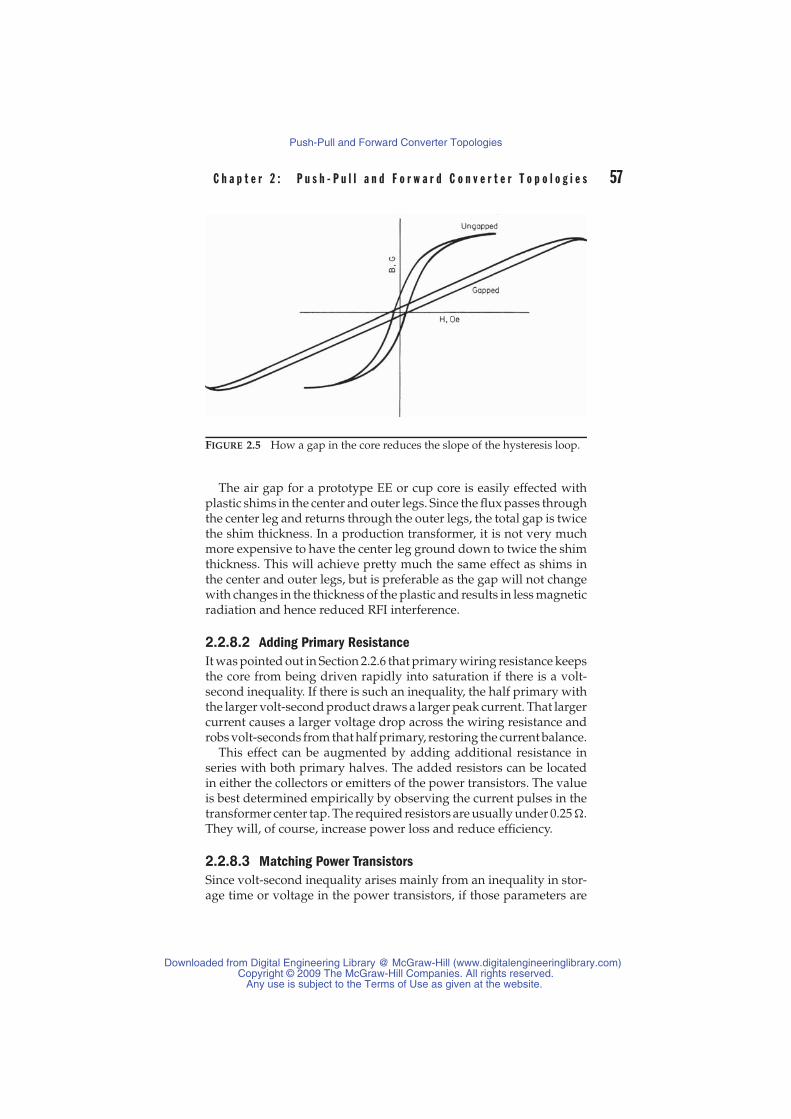
C h a p t e r 2 : P u s h - P u l l a n d F o r w a r d C o n v e r t e r T o p o l o g i e s 57
FIGURE 2.5 How a gap in the core reduces the slope of the hysteresis loop.
The air gap for a prototype EE or cup core is easily effected withplastic shims in the center and outer legs. Since the flux passes throughthe center leg and returns through the outer legs, the total gap is twicethe shim thickness. In a production transformer, it is not very muchmore expensive to have the center leg ground down to twice the shimthickness. This will achieve pretty much the same effect as shims inthe center and outer legs, but is preferable as the gap will not changewith changes in the thickness of the plastic and results in less magneticradiation and hence reduced RFI interference.
2.2.8.2 Adding Primary ResistanceIt was pointed out in Section 2.2.6 that primary wiring resistance keepsthe core from being driven rapidly into saturation if there is a volt-second inequality. If there is such an inequality, the half primary withthe larger volt-second product draws a larger peak current. That largercurrent causes a larger voltage drop across the wiring resistance androbs volt-seconds from that half primary, restoring the current balance.
This effect can be augmented by adding additional resistance inseries with both primary halves. The added resistors can be locatedin either the collectors or emitters of the power transistors. The valueis best determined empirically by observing the current pulses in thetransformer center tap. The required resistors are usually under 0.25�.They will, of course, increase power loss and reduce efficiency.
2.2.8.3 Matching Power TransistorsSince volt-second inequality arises mainly from an inequality in stor-age time or voltage in the power transistors, if those parameters are
Downloaded from Digital Engineering Library @ McGraw-Hill (www.digitalengineeringlibrary.com)Copyright © 2009 The McGraw-Hill Companies. All rights reserved.
Any use is subject to the Terms of Use as given at the website.
Push-Pull and Forward Converter Topologies

58 S w i t c h i n g P o w e r S u p p l y D e s i g n
matched, it adds confidence that together with the earlier two “fixes”there will be no problem with flux imbalance.
This is not a good solution and would be an expensive fix as it isquite expensive to match transistors in two parameters. To do suchmatching requires a specialized test setup that would not be availableif field replacements become necessary.
It also must be ascertained that if the matching is done at certainload currents and temperature, the matching still holds when thesevary. Further, a storage time match is difficult to make credible, as itdepends strongly on forward and reverse base input currents in thebipolar transistors. Generally any matching is done by matching Vceand Vbe (the “on” collector-to-emitter and base-to-emitter voltages)at the maximum operating current. Hence matching is not a viablesolution for high-volume commercial supplies.
2.2.8.4 Using MOSFET Power TransistorsSince most of the volt-second inequality arises from storage timeinequality between the two bipolar power transistors, the problemlargely disappears if MOSFETs are used, because they have no stor-age time.
There is an added advantage, as the “on” voltage of a MOSFET tran-sistor increases with temperature. Thus if one half primary tends totake a large current, its transistor runs somewhat warmer and its “on”voltage increases and steals voltage from the winding. This reducesthe volt-second product on that side and tends to restore balance. This,of course, is qualitatively in the right direction, which is helpful butcannot be depended on to solve the flux-imbalance problem reliablyat all power levels and with a worst-case combination.
However, with power MOSFETs at power levels under 100 W andlow input voltages (as in most DC/DC converter applications), push-pull converters can be and are built with a high degree of confidence.
2.2.8.5 Using Current-Mode TopologyBy far the best solution to the flux-imbalance problem is to use current-mode control. This completely and reliably solves the flux-imbalanceproblem; also it has significant additional advantages of its own.
In conventional push-pull, there is always a residual concern thatdespite all the fixes, a flux-imbalance problem will arise in someworst-case situation and a transistor will be destroyed. Current-modetopology solves this problem by monitoring the current in each ofthe push-pull transistors on a pulse-by-pulse basis. The control cir-cuit then forces alternate current pulses to have equal amplitude,maintaining the working point very near the center of the B/H loop.Details of current-mode topology will be discussed in Chapter 5.
Downloaded from Digital Engineering Library @ McGraw-Hill (www.digitalengineeringlibrary.com)Copyright © 2009 The McGraw-Hill Companies. All rights reserved.
Any use is subject to the Terms of Use as given at the website.
Push-Pull and Forward Converter Topologies

C h a p t e r 2 : P u s h - P u l l a n d F o r w a r d C o n v e r t e r T o p o l o g i e s 59
2.2.9 Power Transformer DesignRelationships
Note The design of wound components is a specialized subject and is cov-ered in more detail in Chapter 7. The correct design of transformers, inductors,and chokes is essential for optimum performance of the equipment. The engi-neer who takes the time to become fully competent in this area will get muchbetter results, so the reader is urged to study Chapter 7 before proceedingwith any real designs.
After Pressman In the following section Mr. Pressman shows an itera-tive method for selecting the core size and winding parameters. It serves asa good example of the rather lengthy process required if this method is used.The reader will do well to study this process, which shows the interactionbetween the various parameters. However, in practice, optimum designs nor-mally start by defining the maximum permitted temperature rise (typically30◦C), and one of the nomogram-assisted methods or computer programswould be used to provide a much faster solution with a defined result, avoid-ing the tedious iterative procedure. ∼ K.B.
2.2.9.1 Core SelectionThe design of a transformer starts with the initial selection of a coreto satisfy the desired total output power. The available output powerfrom a particular core depends on the operating frequency, the oper-ating flux density swing (B1 and B2 in Figure 2.3), the core’s area Ae,the bobbin winding window area Ab, and the current density in eachwinding.
Decisions on each of these parameters are interrelated, and choicesare made to minimize the transformer size and its temperature rise.In the magnetics section of Chapter 7 an equation is derived showinga recommended output power for a given core as a function of theparameters mentioned earlier.
The equation can be used in a set of iterative calculations, first mak-ing a tentative selection of a specific core, peak flux density, and oper-ating frequency, and calculating the available output power. Then ifthe available power is insufficient, a larger-sized core is selected andthe calculations repeated until a core with the required output poweris found.
This is a long and cumbersome procedure; instead the equation isturned into a set of charts that permit a core and operating frequencyto be selected at a glance for any desired output power. Such equationsand charts will be found for most of the commonly used topologiesin Chapter 7.
Downloaded from Digital Engineering Library @ McGraw-Hill (www.digitalengineeringlibrary.com)Copyright © 2009 The McGraw-Hill Companies. All rights reserved.
Any use is subject to the Terms of Use as given at the website.
Push-Pull and Forward Converter Topologies

60 S w i t c h i n g P o w e r S u p p l y D e s i g n
We will assume that these charts will be used to select a specificcore so that the area Ae is known. The rest of the transformer designinvolves calculation of the number of turns on the primary and sec-ondaries, selection of wire sizes, calculation of core and copper losses,and finally the calculation of transformer temperature rise.
The optimum arrangement of the various layers of wire on the corebobbin is important in improving coupling between the windingsand in reducing copper losses due to “skin” and “proximity” effects.Winding arrangements, skin, and proximity effects will be discussedin Chapter 7.
For this example, the design will proceed using the core chosenfrom the selection charts described earlier, providing a known valueof the core area Ae .
2.2.9.2 Maximum Power Transistor On-Time SelectionEquation 2.1 has shown that the converter keeps the output voltageVm constant by increasing Ton as Vdc decreases. Thus the maximum“on” time Ton occurs at the minimum specified DC input voltage Vdc .But in this type of converter the maximum “on” time must not exceedhalf the switching period T . If it were to do so, the reset volt-secondproduct would be less than the set volt-second product (see Section2.2.5), and after a very few cycles, the core would drift into saturationand destroy a power transistor.
Moreover, because of the inevitable storage time in bipolar transis-tors, the base drive “on” time cannot be as large as a full half period, asthe storage time would cause an overlap with the opposite transistor.This would result in immediate failure, because the two power transis-tors would effectively short out the winding. Each transistor wouldtake large currents at the full supply voltage and would rapidly bedestroyed.
Thus, to ensure that the core will always be reset within one periodand eliminate any possibility of simultaneous conduction, wheneverthe DC input voltage is at its minimum Vdc and the feedback loop istrying to increase Ton to maintain Vm constant, the maximum “on” timewill be constrained by some kind of a clamp so as to never be morethan 80% of a half period. Then in Eq. 2.1, for the specified Vdc, T andfor Ton = 0.8T/2, the ratio Nm/Np will be fixed to yield the desiredoutput Vm.
TIP Modern drive and control ICs provide adjustable (so-called) “deadtime” to prevent power device overlap. In some designs, dynamic methods areprovided such that the state of conduction of the power devices is monitoredand the drive signal is delayed until the previous active power device hasturned fully “off,” before the next is allowed to turn “on.” This allows the full
Downloaded from Digital Engineering Library @ McGraw-Hill (www.digitalengineeringlibrary.com)Copyright © 2009 The McGraw-Hill Companies. All rights reserved.
Any use is subject to the Terms of Use as given at the website.
Push-Pull and Forward Converter Topologies

C h a p t e r 2 : P u s h - P u l l a n d F o r w a r d C o n v e r t e r T o p o l o g i e s 61
range of duty cycle to be utilized while completely eliminating any possibilityof overlap. ∼ K.B.
2.2.9.3 Primary Turns SelectionThe number of primary turns is determined by Faraday’s law (see Eq.1.17). From it Np is fixed by the minimum voltage across the primary(Vdc − 1) and the maximum “on” time, which, as earlier, is to be nomore than 0.8T/2. Then
Np = (Vdc − 1)(0.8T/2) × 108
Aed B(2.7)
Since Ae in Eq. 2.7 is fixed by the selected core, Vdc and T are specifiedand the number of primary turns is fixed as soon as dB (the desiredflux change in 0.8T/2) is decided on. This decision is made as follows.
TIP The reader may prefer to use a dimensionally modified version ofFaraday’s law that provides turns directly as follows:
N = VTon
Ae�B
Where N = turnsV = voltage across the winding (Vdc)Ton = maximum “on” period, microseconds�B = flux density swing, teslas (1 tesla = 10,000 gauss)Ae = effective core area, mm2
For all magnetic calculations, I prefer to work in the preceding modified SIunits, as these yield immediate solutions, avoiding the unwieldy exponents,thus reducing errors. ∼ K.B.
2.2.9.4 Maximum Flux Change (Flux Density Swing) SelectionFrom Eq. 2.7, it is seen that the number of primary turns is inverselyproportional to dB, the flux swing. It would seem desirable to maxi-mize dB so as to minimize Np, since fewer turns would mean that alarger wire size could be used, resulting in higher permissible currentsand more output from a given core. Also, fewer turns would result ina less expensive transformer and lower stray parasitic capacities.
From the hysteresis loop of Figure 2.3, however, it is seen that inferrite cores, the loop enters the curved portion above ± 2000 G. Itis desirable to stay below this point, where the magnetizing currentstarts increasing rapidly. So initially a good choice would appear tobe ± 2000 G (0.2 tesla). But we must also consider core losses.
Ferrite core losses increase at about the 2.7th power of the peakflux density and at about the 1.6th power of the operating frequency.
Downloaded from Digital Engineering Library @ McGraw-Hill (www.digitalengineeringlibrary.com)Copyright © 2009 The McGraw-Hill Companies. All rights reserved.
Any use is subject to the Terms of Use as given at the website.
Push-Pull and Forward Converter Topologies

62 S w i t c h i n g P o w e r S u p p l y D e s i g n
Hence, up to about 50 kHz, core losses do not prohibit operation to± 2000 G, and it may appear desirable to operate at that flux level.
However, to prevent core saturation under transient conditions, itis better to provide a wider margin. We will see shortly that it is prefer-able to restrict operation to ± 1600 G even at frequencies where corelosses are not prohibitive. Faraday’s law solved for the flux changedB is
dB = (Vdc − 1)(Ton) × 108
Np Ae(2.8)
Equation 2.8 says that if Np is chosen for a given dB—say, from−2000 to +2000 G, or a dB of 4000 G, then as long as the productof (Vdc − 1)(Ton) is constant, dB will be constant at 4000 G. Further,if the feedback loop is working and keeping the output voltage Vmconstant, Eq. 2.1 says that (Vdc − 1)(Ton) is constant and dB will trulyremain constant. So providing the feedback loop always ensures thatwhenever Vdc is a minimum, that Ton is at a maximum, then Ton andVdc can never be simultaneously maximum.
However, in some transient or fault conditions, if Ton has been atmaximum for a single, or possibly even a few cycles, and Vdc had atransient step to 50% above its normal value, the feedback loop mayfail to reduce the “on” time rapidly enough (as normally required byEq. 2.1), and there may exist a short period when Vdc and Ton wouldbe maximum at the same time. In this event, Equation 2.8 shows thatdB would be 1.5(4000) or 6000 G.
Then if the core had started from the −2000-G point, at the endof that “on” time the core would have been driven 6000 G abovethat, or to +4000 G. The hysteresis loop (see Figure 2.3) shows that attemperatures somewhat above 25◦C, it would be deep in saturationand could not support the applied voltage. The transistor would besubject to high current and high voltage and would rapidly fail.
It will be seen in the feedback analysis section of Chapter 12 that theerror amplifier has a delay in its response time, because its bandwidthis limited to stabilize the feedback loop. Hence, it is always possible forboth the input voltage and “on” time to be maximum for a transientperiod due to the inevitable delay in the response of the error amplifier,although the error amplifier will eventually correct the “on” time soas to keep the product (Vdc − 1)(Ton) constant in accordance with Eq.2.1. If the core is subjected to maximum input voltage and maximum“on” time as a result of error-amplifier delay, even for a single cycle,it may saturate the core and destroy a transistor.
However if Np in Eq. 2.8 is chosen to yield dB of 3200 G at Vdc andTon, the design is safer and can tolerate a 50% transient step in inputvoltage. With dB = 3200 G, if the error amplifier is too slow to correct
Downloaded from Digital Engineering Library @ McGraw-Hill (www.digitalengineeringlibrary.com)Copyright © 2009 The McGraw-Hill Companies. All rights reserved.
Any use is subject to the Terms of Use as given at the website.
Push-Pull and Forward Converter Topologies

C h a p t e r 2 : P u s h - P u l l a n d F o r w a r d C o n v e r t e r T o p o l o g i e s 63
the “on” time, the transformer dB will be 1.5(3200) or 4800 G; and ifthe core started from its normal minimum flux of −1600 G, it will bedriven up to only −1600 + 4800 or +3200 G. The hysteresis loop ofFigure 2.3 shows that the core can tolerate that even at 100◦C.
Thus the number of primary turns is selected from Eq. 2.7 for dB =3200 G even at lower frequencies where a large flux may not causeexcessive core losses. Above 50 kHz, the core losses increase rapidlyand force a lower flux density selection. At 100 to 200 kHz, the peakflux density may be limited to 1200 or even 800 G to achieve an ac-ceptably low core temperature rise.
2.2.9.5 Secondary Turns SelectionThe turns for the main and slave outputs are calculated from Eqs. 2.1,2.2, and 2.3 in accordance with the specified, or calculated, voltagerequirements. We see that the input voltage Vdc and T have been spec-ified. The maximum “on” time Ton has been arbitrarily set at 0.8T/2,and Np has been calculated from Faraday’s law (see Eq. 2.7) for theknown Ae for the selected core. Flux swing dB has been set at 3200 G forfrequencies under 50 kHz and to minimize core losses. Lower valueswill be used at higher frequencies as discussed earlier.
2.2.10 Primary, Secondary Peakand rms Currents
In this example, wire sizes will be selected on the basis of a conser-vative operating current density. Current density is given in terms ofrms current in amps per circular mil∗ of wire cross-sectional area.
Hence, before we can start selecting wire sizes for any winding, werequire a knowledge of the rms currents in each winding.
2.2.10.1 Primary Peak Current CalculationCurrent drawn from the DC input source Vdc may be monitored in thetransformer center tap and has the waveform shown in Figures 2.1band 2.1d. The pulses have the characteristic ramp-on-a-step wave-shape because the secondaries all have output LC filters as discussedin Section 1.3.2. The primary current is simply the sum of all the sec-ondary ramp-on-a-step currents reflected into the primary by theirturns ratios, plus the magnetizing current.
As discussed in Section 2.2.9.2, at minimum Vdc input voltage, thetransistor “on” times will be 80% of a half period. Further, since there isone pulse for each half period, the duty cycle of the pulses in Figure 2.1
∗A circular mil is the area of a circle 1 mil in diameter. Thus, area in squareinches = (π/4)10−6 (area in circular mils).
Downloaded from Digital Engineering Library @ McGraw-Hill (www.digitalengineeringlibrary.com)Copyright © 2009 The McGraw-Hill Companies. All rights reserved.
Any use is subject to the Terms of Use as given at the website.
Push-Pull and Forward Converter Topologies

64 S w i t c h i n g P o w e r S u p p l y D e s i g n
is 0.8 at Vdc. To simplify calculation, the pulses in the figure areassumed to have an equivalent flat-topped waveshape whose am-plitude Ipft is the value of the current at the center of the ramp.
Then the input power at Vdc is that voltage times the average cur-rent, which is 0.8Ipft, and assuming 80% efficiency (which is usuallyachievable up to 200 kHz), Po = 0.8Pin or
Pin = 1.25Po = Vdc0.8Ipft
Then
Ipft = 1.56Po
Vdc(2.9)
This is a useful relation, as it gives the equivalent flat-topped pri-mary current pulse amplitude in terms of what is known—the outputpower and the specified minimum DC input voltage. It allows selec-tion of a primary wire size from the calculated primary rms current. Italso allows a transistor with an adequate current rating to be selected.
2.2.10.2 Primary rms Current Calculationand Wire Size Selection
Each half primary carries only one of the Ipft pulses per period, andhence its duty cycle is (0.8T/2)/T or 0.4. It is well known that the rmsvalue of a flat-topped pulse of amplitude Ipft at a duty cycle D is
Irms = Ipft√
D = Ipft√
0.4
or
Irms = 0.632Ipft (2.10)
and from Eq. 2.9
Irms = 0.6321.56Po
Vdc= 0.986Po
Vdc(2.11)
This gives the rms current in each half primary in terms of the knownparameters: output power and the specified minimum DC inputvoltage.
A conservative practice in transformer design is to operate thewindings at a current density of 500 circular mils per rms ampere.There is nothing absolute about this; current densities of 300 circularmils per rms ampere are frequently used for windings with only a fewturns. As a general rule, however, densities greater than 300 circularmils per rms ampere should be avoided, as that will cause excessivecopper losses and temperature rise.
Downloaded from Digital Engineering Library @ McGraw-Hill (www.digitalengineeringlibrary.com)Copyright © 2009 The McGraw-Hill Companies. All rights reserved.
Any use is subject to the Terms of Use as given at the website.
Push-Pull and Forward Converter Topologies
C h a p t e r 2 : P u s h - P u l l a n d F o r w a r d C o n v e r t e r T o p o l o g i e s 65
Thus at 500 circular mils per rms ampere, the required number ofcircular mils for the half primaries is
Circular mils = 5000.986 Po
Vdc
= 493Po
Vdc
(2.12)
Notice that this is also in terms of known values—output power andspecified minimum DC input voltage. Proper wire size can then bechosen from wire tables at the circular mils given by Eq. 2.12.
2.2.10.3 Secondary Peak, rms Current, and Wire Size CalculationCurrents in each half secondary are shown in Figure 2.6. Note theledge at the end of the transistor “on” time. This ledge of current existsbecause there is no free-wheeling diode D1 at the input to the filterinductor as in the buck regulator of Figure 1.4. In the buck, the free-wheeling diode was essential as a return path for inductor currentwhen the transistor turned off. When the transistor turned off, thepolarity across the output inductor reversed, and its input end wouldhave gone disastrously negative if it had not been caught by the free-wheeling diode at about 1 V below ground. Inductor current thencontinued to flow through the free-wheeling diode D1 of Figure 1.4e.This problem does not exist in the rectifier circuit shown in Figure 2.6.
In the push-pull output rectifier stage, the function of the free-wheeling diode is performed by the output rectifier diodes D1 andD2. When either transistor turns “off,” the input end of the inductortries to go negative. As soon as it goes about one diode drop belowground, both rectifiers conduct, each drawing roughly half the totalcurrent the inductor had been drawing just prior to turn “off” (seeFigures 2.6d and 2.6e). Since the impedance of each half secondaryis small, there is negligible drop across them, and the rectifier diodecathodes are caught at about 1 V below ground.
Thus if half-secondary rms currents are to be calculated exactly, theledge currents during the 20% dead time should be taken into account.However, in this example it can be seen that they are only about halfthe peak inductor current and have a duty cycle of (0.4T/2)/T or 0.2.With such small amplitudes and duty cycle they can be ignored inthis example. Each half secondary can then be considered to havethe characteristic ramp-on-a-step waveform, which at minimum DCinput comes out to a duty cycle of (0.8T/2)/T or 0.4. The magnitudeof the current at the center of the ramp is the DC output current Idc,as can be seen from Figure 2.6 f.
Downloaded from Digital Engineering Library @ McGraw-Hill (www.digitalengineeringlibrary.com)Copyright © 2009 The McGraw-Hill Companies. All rights reserved.
Any use is subject to the Terms of Use as given at the website.
Push-Pull and Forward Converter Topologies
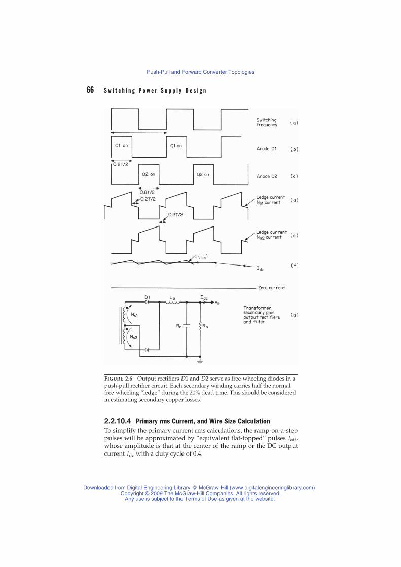
66 S w i t c h i n g P o w e r S u p p l y D e s i g n
FIGURE 2.6 Output rectifiers D1 and D2 serve as free-wheeling diodes in apush-pull rectifier circuit. Each secondary winding carries half the normalfree-wheeling “ledge” during the 20% dead time. This should be consideredin estimating secondary copper losses.
2.2.10.4 Primary rms Current, and Wire Size CalculationTo simplify the primary current rms calculations, the ramp-on-a-steppulses will be approximated by “equivalent flat-topped” pulses Iaft,whose amplitude is that at the center of the ramp or the DC outputcurrent Idc with a duty cycle of 0.4.
Downloaded from Digital Engineering Library @ McGraw-Hill (www.digitalengineeringlibrary.com)Copyright © 2009 The McGraw-Hill Companies. All rights reserved.
Any use is subject to the Terms of Use as given at the website.
Push-Pull and Forward Converter Topologies
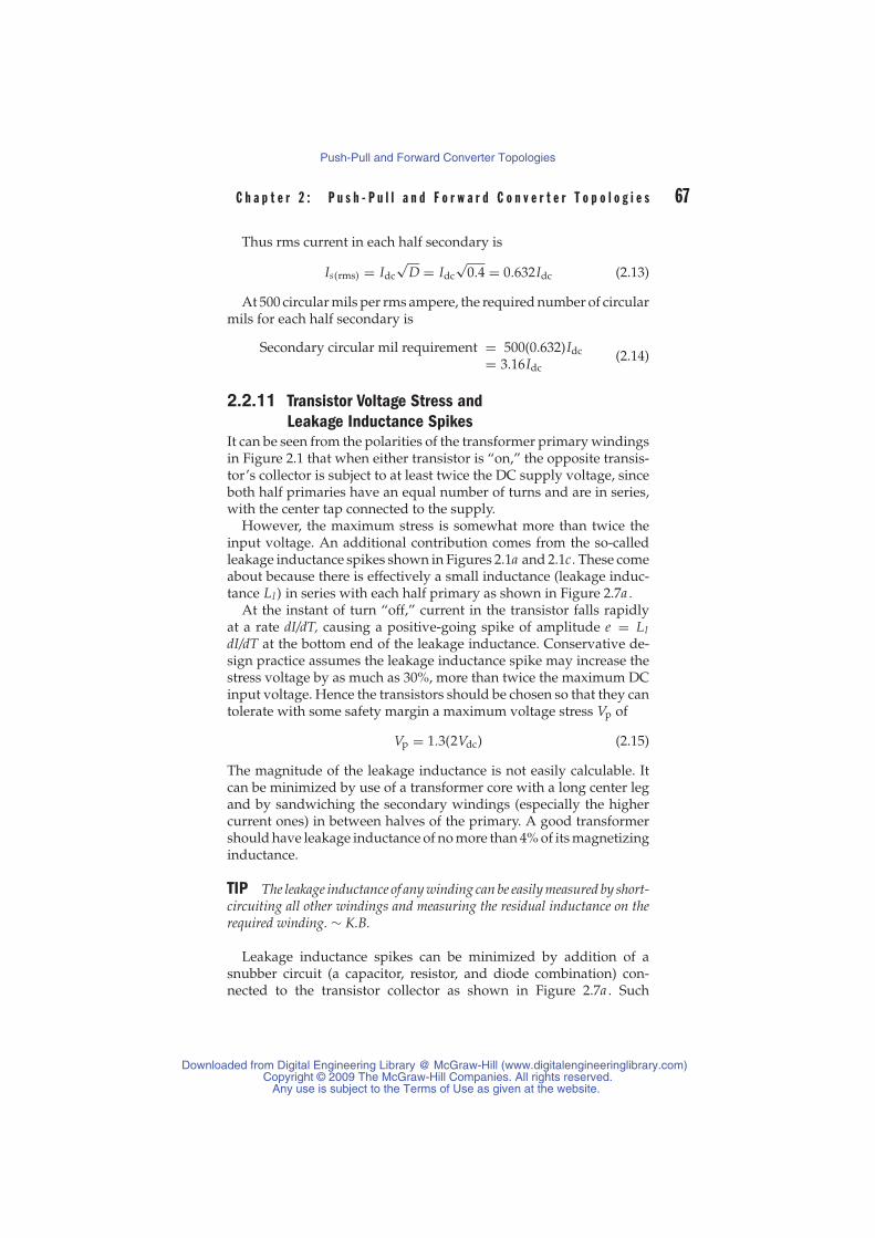
C h a p t e r 2 : P u s h - P u l l a n d F o r w a r d C o n v e r t e r T o p o l o g i e s 67
Thus rms current in each half secondary is
Is(rms) = Idc√
D = Idc√
0.4 = 0.632Idc (2.13)
At 500 circular mils per rms ampere, the required number of circularmils for each half secondary is
Secondary circular mil requirement = 500(0.632)Idc= 3.16Idc
(2.14)
2.2.11 Transistor Voltage Stress andLeakage Inductance Spikes
It can be seen from the polarities of the transformer primary windingsin Figure 2.1 that when either transistor is “on,” the opposite transis-tor’s collector is subject to at least twice the DC supply voltage, sinceboth half primaries have an equal number of turns and are in series,with the center tap connected to the supply.
However, the maximum stress is somewhat more than twice theinput voltage. An additional contribution comes from the so-calledleakage inductance spikes shown in Figures 2.1a and 2.1c. These comeabout because there is effectively a small inductance (leakage induc-tance Ll ) in series with each half primary as shown in Figure 2.7a .
At the instant of turn “off,” current in the transistor falls rapidlyat a rate dI/dT, causing a positive-going spike of amplitude e = LldI/dT at the bottom end of the leakage inductance. Conservative de-sign practice assumes the leakage inductance spike may increase thestress voltage by as much as 30%, more than twice the maximum DCinput voltage. Hence the transistors should be chosen so that they cantolerate with some safety margin a maximum voltage stress Vp of
Vp = 1.3(2Vdc) (2.15)
The magnitude of the leakage inductance is not easily calculable. Itcan be minimized by use of a transformer core with a long center legand by sandwiching the secondary windings (especially the highercurrent ones) in between halves of the primary. A good transformershould have leakage inductance of no more than 4% of its magnetizinginductance.
TIP The leakage inductance of any winding can be easily measured by short-circuiting all other windings and measuring the residual inductance on therequired winding. ∼ K.B.
Leakage inductance spikes can be minimized by addition of asnubber circuit (a capacitor, resistor, and diode combination) con-nected to the transistor collector as shown in Figure 2.7a . Such
Downloaded from Digital Engineering Library @ McGraw-Hill (www.digitalengineeringlibrary.com)Copyright © 2009 The McGraw-Hill Companies. All rights reserved.
Any use is subject to the Terms of Use as given at the website.
Push-Pull and Forward Converter Topologies
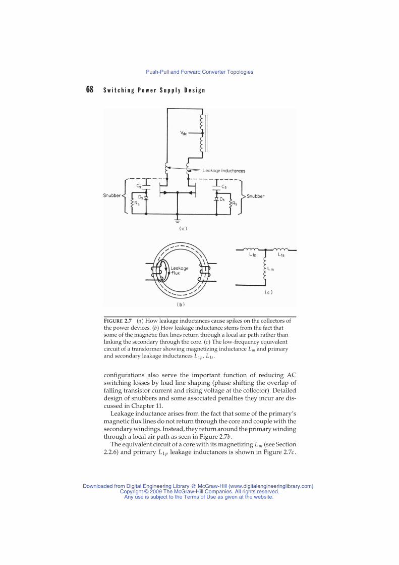
68 S w i t c h i n g P o w e r S u p p l y D e s i g n
FIGURE 2.7 (a ) How leakage inductances cause spikes on the collectors ofthe power devices. (b) How leakage inductance stems from the fact thatsome of the magnetic flux lines return through a local air path rather thanlinking the secondary through the core. (c) The low-frequency equivalentcircuit of a transformer showing magnetizing inductance Lm and primaryand secondary leakage inductances L1p, L1s .
configurations also serve the important function of reducing ACswitching losses by load line shaping (phase shifting the overlap offalling transistor current and rising voltage at the collector). Detaileddesign of snubbers and some associated penalties they incur are dis-cussed in Chapter 11.
Leakage inductance arises from the fact that some of the primary’smagnetic flux lines do not return through the core and couple with thesecondary windings. Instead, they return around the primary windingthrough a local air path as seen in Figure 2.7b.
The equivalent circuit of a core with its magnetizing Lm (see Section2.2.6) and primary L1p leakage inductances is shown in Figure 2.7c.
Downloaded from Digital Engineering Library @ McGraw-Hill (www.digitalengineeringlibrary.com)Copyright © 2009 The McGraw-Hill Companies. All rights reserved.
Any use is subject to the Terms of Use as given at the website.
Push-Pull and Forward Converter Topologies
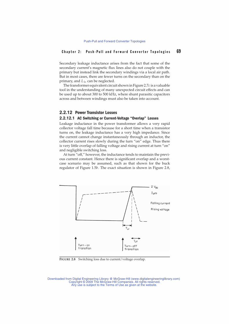
C h a p t e r 2 : P u s h - P u l l a n d F o r w a r d C o n v e r t e r T o p o l o g i e s 69
Secondary leakage inductance arises from the fact that some of thesecondary current’s magnetic flux lines also do not couple with theprimary but instead link the secondary windings via a local air path.But in most cases, there are fewer turns on the secondary than on theprimary, and L1s can be neglected.
The transformer equivalent circuit shown in Figure 2.7c is a valuabletool in the understanding of many unexpected circuit effects and canbe used up to about 300 to 500 kHz, where shunt parasitic capacitorsacross and between windings must also be taken into account.
2.2.12 Power Transistor Losses2.2.12.1 AC Switching or Current-Voltage “Overlap” LossesLeakage inductance in the power transformer allows a very rapidcollector voltage fall time because for a short time when a transistorturns on, the leakage inductance has a very high impedance. Sincethe current cannot change instantaneously through an inductor, thecollector current rises slowly during the turn “on” edge. Thus thereis very little overlap of falling voltage and rising current at turn “on”and negligible switching loss.
At turn “off,” however, the inductance tends to maintain the previ-ous current constant. Hence there is significant overlap and a worst-case scenario may be assumed, such as that shown for the buckregulator of Figure 1.5b. The exact situation is shown in Figure 2.8,
FIGURE 2.8 Switching loss due to current/voltage overlap.
Downloaded from Digital Engineering Library @ McGraw-Hill (www.digitalengineeringlibrary.com)Copyright © 2009 The McGraw-Hill Companies. All rights reserved.
Any use is subject to the Terms of Use as given at the website.
Push-Pull and Forward Converter Topologies

70 S w i t c h i n g P o w e r S u p p l y D e s i g n
where it is assumed that the current hangs on at its equivalent flat-topped peak value Ipft (see Section 2.2.10.1) for the time it takes thevoltage to rise from near zero to its maximum value of 2Vdc. The volt-age then remains at 2Vdc during the time, Tcf, it takes the current tofall from Ipft to zero. Assuming Tvr = Tcf = Ts and a switching periodT, the total switching dissipation per transistor per period Pt(ac) is
Pt(ac) = Ipft2Vdc
2Ts
T+ 2Vdc
Ipft
2Ts
T
= 2( Ipft)(Vdc)Ts
T
and from Eq. 2.9, Ipft = 1.56( Po/Vdc):
Pt(ac) = 3.12Po
VdcVdc
Ts
T(2.16)
Notice there are negligible switching losses at turn “on” becausetransformer leakage inductance causes a very fast voltage fall and aslow current rise. This results in very little turn “on” loss. However,worst-case scenario is shown at turn “off.” The current remains con-stant at its peak Ipft until voltages rises to 2Vdc. The voltage remainsat 2Vdc for the duration of the current fall time Tcf, producing a largeturn “off” loss.
2.2.12.2 Transistor Conduction LossesThe conduction losses are simply the transistor “on” voltage multi-plied by the “on” current for each device averaged over a cycle, or
Pdc = IpftVon0.8T/2
T= 0.4IpftVon
It will be seen in Chapter 8 that a technique called Baker clamping canbe used to reduce transistor storage times for bipolar base drives. Thisforces the collector “on” potential Vce to be about 1 V over a large rangeof current. Then for Ipft from Eq. 2.9 we obtain
Pdc = 0.41.56Po
Vdc= 0.624Po
Vdc(2.17)
and total losses per transistor are
Ptotal = Pt(ac) + Pdc
= 3.12Po
VdcVdc
Ts
T+ 0.624Po
Vdc
(2.18)
Downloaded from Digital Engineering Library @ McGraw-Hill (www.digitalengineeringlibrary.com)Copyright © 2009 The McGraw-Hill Companies. All rights reserved.
Any use is subject to the Terms of Use as given at the website.
Push-Pull and Forward Converter Topologies

C h a p t e r 2 : P u s h - P u l l a n d F o r w a r d C o n v e r t e r T o p o l o g i e s 71
2.2.12.3 Typical Losses: 150-W, 50-kHz Push-Pull ConverterIt will be instructive to calculate the dissipation per transistor in a150-W push-pull converter at 50 kHz operating from a 48-volt powersource.
The standard telephone industry power sources provide a nominalvoltage of 48 V, with a minimum (Vdc) of 38 V and maximum (Vdc) of60 V. It will be assumed that at 50 kHz, bipolar transistors will be used,and a reasonable value of the switching time (Ts as defined earlier) of0.3 μs.
The DC conduction losses from Eq. 2.17 are
Pdc = 0.624 × 15038
= 2.46 W
but the AC switching losses from Eq. 2.16 are much larger at
Pt(ac) = 3.12 × 15038
× 60 × 0.320
= 11.8 W
Thus the AC overlap or switching losses are about 4.5 times greaterthan the DC conduction losses. If MOSFET transistors are consideredwith switching times Ts of about 0.05 μs, it can be seen that switchinglosses would be negligible in this example.
2.2.13 Output Power and Input VoltageLimitations in the Push-Pull Topology
Aside from the flux-imbalance problem in the push-pull topology,which does not exist in the current-mode controlled version, limita-tions include the useful power working area as defined in Eq. 2.9, andinput voltage in Eq. 2.15.
Equation 2.9 gives the peak current required of the transistor fora desired output power, and Eq. 2.15 gives the maximum voltagestress on the transistor in terms of the maximum DC input voltage.These requirements limit the power rating of the push-pull topologyto around 500 W when using bipolar transistors. Above that, it isdifficult to find transistors that can meet the peak current and voltagestress while being fast enough with adequate gain.
The technology is constantly improving, and without doubt a fasterMOSFET with adequately high voltage and current ratings and suffi-ciently low “on” voltages would extend this power range.
As an example, we will consider a 400-W push-pull converter op-erating from telephone industry prime voltage source that is 48 V(nominal), 38 V (minimum), and 60 V (maximum).
Downloaded from Digital Engineering Library @ McGraw-Hill (www.digitalengineeringlibrary.com)Copyright © 2009 The McGraw-Hill Companies. All rights reserved.
Any use is subject to the Terms of Use as given at the website.
Push-Pull and Forward Converter Topologies

72 S w i t c h i n g P o w e r S u p p l y D e s i g n
Equation 2.9 gives the peak current requirement as Ipft =1.56Po/Vdc = 1.56(400)/38 = 16.4 A, and Eq. 2.15 gives the maxi-mum “off” voltage stress as Vp = 2.6Vdc = 2.6 × 60 = 156 V. Toprovide a margin of safety, a transistor with at least a 200-V ratingwould be selected.
A possible candidate would be the MJ13330 bipolar transistor. Ithas a 20-A peak current rating, a Vceo rating of 200 V, and Vcer ratingof 400 V (the voltage it can sustain when it has a negative bias of −1to −5 V at turn “off”). It can thus meet the peak voltage and currentstresses.
At 16 amps, it has a maximum “on” saturation voltage of about 3 V,a minimum gain of about 5, and a storage time of 1.3 to 4 μs. How-ever, with these limitations, it would have high DC and AC switchinglosses, have difficulty with flux imbalance (unless the current-modeversion of push-pull were used), and would have difficulty operatingabove 40 kHz because of the long storage times.
A potential MOSFET for such an application is the MTH30N20.This is a 30-A, 200-V device that at 16 A would have only 1.3 V “on”state voltage drop and hence half the DC conduction losses of thepreceding bipolar transistor. With its fast switching times it wouldhave quite low switching losses, but this and similar devices can bequite expensive.
For offline converters, the push-pull topology is not very attractivedue to the large voltage stress of 2.6Vdc (see Eq. 2.15). For example,with a 120-V AC line input and ± 10% tolerance, the peak rectified DCvoltage is 1.41 × 1.1 × 120 = 186 V. Hence during turn “off” at the topof the leakage spike, Eq. 2.15 gives a peak stress of 2.6 × 186 = 484 V.
We must also allow for transients in the supply above the maximumsteady-state values. Transients are seldom specified for commercialpower supplies, but conservative design practice assumes stress atleast 15% above the maximum steady-state value, increasing the max-imum stress to 1.15 × 484 or 557 V.
Input voltage transients in special cases can be even greater, for ex-ample, the specifications on military aircraft given by Military Stan-dard 704. Here the nominal voltage is 113 V AC but with a 10-mstransient to 180 V AC, the peak “off” stress from Eq. 1.42 would be180 × 1.41 × 2.6 or 660 V. Although there are many fast bipolar tran-sistors that can safely sustain voltages as high as 850 V with reverseinput bias, clearly it is not good practice to use a topology that subjectsthe transistors to high voltage transients.
Some topologies subject the transistors to only the normal maxi-mum DC input voltage stress with no leakage spike. These are a betterchoice for high voltage and “offline” applications, not only because ofthe lesser voltage stress, but also because the smaller voltage excursionat turn “off” produces less EMI (electromagnetic interference).
Downloaded from Digital Engineering Library @ McGraw-Hill (www.digitalengineeringlibrary.com)Copyright © 2009 The McGraw-Hill Companies. All rights reserved.
Any use is subject to the Terms of Use as given at the website.
Push-Pull and Forward Converter Topologies
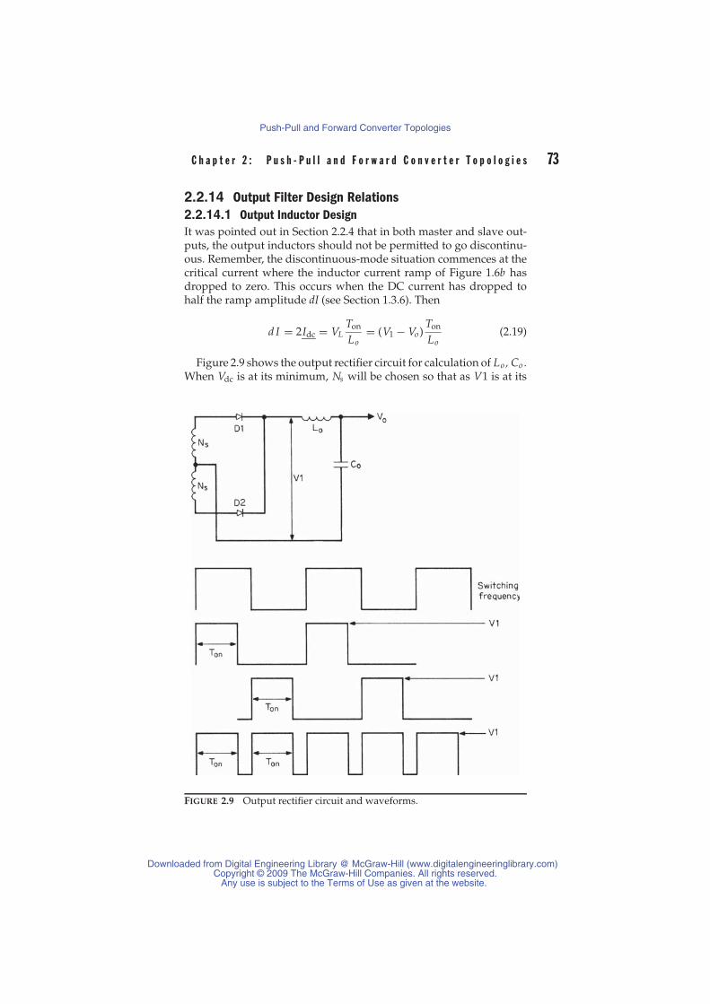
C h a p t e r 2 : P u s h - P u l l a n d F o r w a r d C o n v e r t e r T o p o l o g i e s 73
2.2.14 Output Filter Design Relations2.2.14.1 Output Inductor DesignIt was pointed out in Section 2.2.4 that in both master and slave out-puts, the output inductors should not be permitted to go discontinu-ous. Remember, the discontinuous-mode situation commences at thecritical current where the inductor current ramp of Figure 1.6b hasdropped to zero. This occurs when the DC current has dropped tohalf the ramp amplitude dI (see Section 1.3.6). Then
d I = 2Idc = VLTon
Lo= (V1 − Vo )
Ton
Lo(2.19)
Figure 2.9 shows the output rectifier circuit for calculation of Lo, Co .
When Vdc is at its minimum, Ns will be chosen so that as V1 is at its
FIGURE 2.9 Output rectifier circuit and waveforms.
Downloaded from Digital Engineering Library @ McGraw-Hill (www.digitalengineeringlibrary.com)Copyright © 2009 The McGraw-Hill Companies. All rights reserved.
Any use is subject to the Terms of Use as given at the website.
Push-Pull and Forward Converter Topologies

74 S w i t c h i n g P o w e r S u p p l y D e s i g n
minimum, Ton will not have to be greater than 0.8T/2 to yield thespecified value of Vo .
But Vo = V1(2Ton/T). Then
Ton = Vo T2V1
But Ns will be chosen so that Ton will be 0.8T/2 when Vdc and conse-quently, V1, are at their minimum so that
Ton = 0.8T2
= Vo T2V1
or V1 = 1.25Vo
and
dI = (1.25Vo − Vo )(0.8T/2)Lo
= 2Idc and Lo = 0.05Vo TIdc
Then if the minimum current Idc is specified as one-tenth the nom-inal current Ion (the usual case),
Lo = 0.5Vo TIon
(2.20)
where Lo is in henriesVo is in voltsT is in secondsIdc is minimum output current in amperesIon is nominal output current in amperes
2.2.14.2 Output Capacitor DesignThe output capacitor Co is selected to meet the maximum output ripplevoltage specification. In Section 1.3.7 it was shown that the outputripple is determined almost completely by the magnitude of the ESR(equivalent series resistance, Ro ) in the filter capacitor and not by themagnitude of the capacitor itself. The peak-to-peak ripple voltage Vris very closely equal to
Vr = RodI (2.21)
where dI is the selected peak-to-peak inductor ramp amplitude.However, it was pointed out that (for aluminum electrolytic ca-
pacitors) the product RoCo has been observed to be relatively con-stant over a large range of capacitor magnitudes and voltage ratings.
Downloaded from Digital Engineering Library @ McGraw-Hill (www.digitalengineeringlibrary.com)Copyright © 2009 The McGraw-Hill Companies. All rights reserved.
Any use is subject to the Terms of Use as given at the website.
Push-Pull and Forward Converter Topologies
C h a p t e r 2 : P u s h - P u l l a n d F o r w a r d C o n v e r t e r T o p o l o g i e s 75
For aluminum electrolytics, the product RoCo ranges between 50 and80 × 10−6. Then Co is selected as
Co = 80 × 10−6
Ro= 80 × 10−6
Vr/dI
= (80 × 10−6)(dI)Vr
(2.22)
where Co is in farads for dI in amperes (see Eq. 2.19) and Vr is in volts.
2.3 Forward Converter Topology2.3.1 Basic OperationA typical triple output forward converter topology is shown inFigure 2.10. This topology is often chosen for output powers under200 W with DC supply voltages in the range of 60 to 200 V. Below60 V, the primary input current becomes uncomfortably large at thehigher power levels. Above about 250 V, the maximum voltage stresson the transistors becomes uncomfortably large.
Further, it will be shown that above output powers of 200 W or so,the primary input current becomes too large even at the higher supplyvoltages. We will see this from the following mathematical analysis.
The topology is similar to the push-pull circuit of Figure 2.1, butdoes not suffer from the latter’s major shortcoming of flux imbalance,since it has one rather than two transistors. Compared with the push-pull, at lower power it is more economical in cost and size.
In Figure 2.10 we see a master output Vom and two slaves, Vs1 andVs2. A negative-feedback loop is closed around the master, and con-trols the Q1 “on” time so as to keep Vom constant against line andload changes. With an “on” time fixed by the master feedback loop,the slave outputs Vs1 and Vs2 are fully regulated against input volt-age changes but only partly (about 5 to 8%) against load changes inthemselves or in the master. The circuit works as follows.
If we compare the forward converter with the push-pull of Figure2.1, we see that one of the transistors has been replaced by the diodeD1. When Q1 is turned “on,” the start of the primary winding Np (thedot end) and the start of all secondaries go positive. Current flows intothe dot end of Np. At the same time, all rectifier diodes D2 to D4 areforward-biased, and current flows out of the starts of all secondariesinto the LC filters and the loads. Note that power flows into the loadswhen the power transistor Q1 is turned “on,” hence the term forwardconverter. Both the push-pull and buck regulators deliver power to
Downloaded from Digital Engineering Library @ McGraw-Hill (www.digitalengineeringlibrary.com)Copyright © 2009 The McGraw-Hill Companies. All rights reserved.
Any use is subject to the Terms of Use as given at the website.
Push-Pull and Forward Converter Topologies
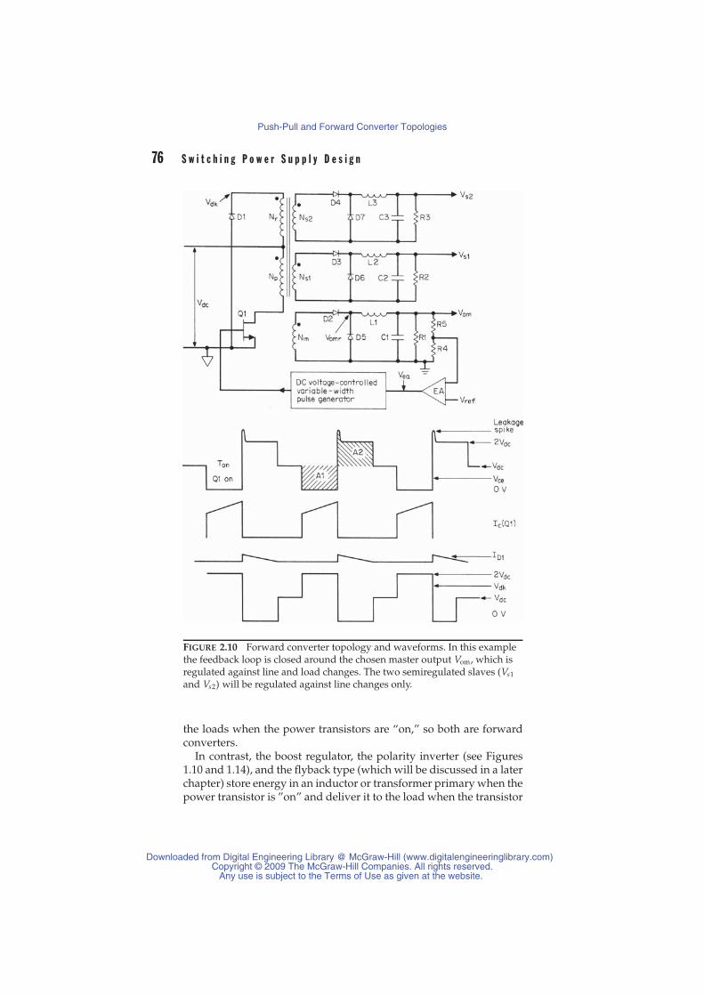
76 S w i t c h i n g P o w e r S u p p l y D e s i g n
FIGURE 2.10 Forward converter topology and waveforms. In this examplethe feedback loop is closed around the chosen master output Vom, which isregulated against line and load changes. The two semiregulated slaves (Vs1
and Vs2) will be regulated against line changes only.
the loads when the power transistors are “on,” so both are forwardconverters.
In contrast, the boost regulator, the polarity inverter (see Figures1.10 and 1.14), and the flyback type (which will be discussed in a laterchapter) store energy in an inductor or transformer primary when thepower transistor is ”on” and deliver it to the load when the transistor
Downloaded from Digital Engineering Library @ McGraw-Hill (www.digitalengineeringlibrary.com)Copyright © 2009 The McGraw-Hill Companies. All rights reserved.
Any use is subject to the Terms of Use as given at the website.
Push-Pull and Forward Converter Topologies

C h a p t e r 2 : P u s h - P u l l a n d F o r w a r d C o n v e r t e r T o p o l o g i e s 77
turns “off.” Such energy storage topologies can operate in either thediscontinuous or continuous mode. These topologies are fundamen-tally different from the forward converters and were discussed in Sec-tions 1.4.2 and 1.4.3. They will be taken up again in Chapter 4, whichcovers the flyback topology.
Consider Figure 2.10: if transistor Q1 has an “on” time of Ton, thevoltage at the master rectifier cathode D5 is at a high level for a periodof Ton. Assuming a 1-V “on” voltage for Q1 and a rectifier forwarddrop of VD2, the high-level voltage Vomr is
Vomr =[
(Vdc − 1)Nm
Np
]− VD2 (2.23)
The circuitry after the rectifier diode cathodes is exactly like thatof the buck regulator of Figure 1.4. Diodes D5 to D7 act like the free-wheeling diode D1 of that figure. When Q1 turns “off,” the currentestablished in the magnetizing inductance of T1 while Q1 was “on”(recall the equivalent circuit of a transformer as in Figure 2.7c) reversesthe polarity of the voltage across Np. Now all the starts (dot ends) ofprimary and secondary windings go negative. Without the “catch”action of diode D1, the dot end of Nr would go very far negative; sinceNp and Nr usually have equal turns, the no-dot end of Np would gosufficiently positive to avalanche Q1 and destroy it.
However, with the catch action of diode D1, the dot end of Nr willbe clamped at one diode drop below ground. If there were no leakageinductance in T1 (recall again the equivalent circuit of a transformeras in Figure 2.7c), the voltage across Np would equal that across Nr .
Assuming that the 1-V forward drop across D1 can be neglected, thevoltage across Nr and Np is Vdc, and the voltage at the no-dot end ofNp and at the Q1 collector is then 2Vdc.
We have seen previously that within one cycle, if a core has movedin one direction on its hysteresis loop, it must be restored to exactlyits original position on the loop before it can be allowed to movein the same direction again in the next cycle. Otherwise, after manycycles, the core will “staircase” into saturation. If this is allowed tohappen, the core will not be able to support the applied voltage, andthe transistor will be destroyed.
Figure 2.10 shows that when Q1 is “on” for a time Ton, Np is sub-jected to volt-second product VdcTon with its dot-end positive, thatvolt-second product is the area A1 in Figure 2.10. By Faraday’s law(see Eq. 1.17), that volt-second product causes—say, a positive—fluxchange dB = (VdcTon/Np Ae )10−8 gauss.
When Q1 turns “off,” and the magnetizing inductance has reversedthe polarity across Np and kept its no-dot end at 2Vdc long enough forthe volt-second area product A2 in Figure 2.10 to equal area A1, thecore has been restored to its original position on the hysteresis loop,
Downloaded from Digital Engineering Library @ McGraw-Hill (www.digitalengineeringlibrary.com)Copyright © 2009 The McGraw-Hill Companies. All rights reserved.
Any use is subject to the Terms of Use as given at the website.
Push-Pull and Forward Converter Topologies
78 S w i t c h i n g P o w e r S u p p l y D e s i g n
and the next cycle can safely start. We can see that the “reset volt-seconds” has equaled the “set volt-seconds.”
When Q1 turns “off,” the dot ends of all secondaries go negativewith respect to their no-dot ends. Current in all output inductors L1to L3 will try to decrease. Since current in inductors cannot change in-stantaneously, the polarity across all inductors reverses in an attemptto maintain the current’s constant. The input ends of the inductorstry to go far negative, but are caught at one diode drop below out-put ground by free-wheeling diodes D5 to D7 (see Figure 2.10), andrectifier diodes D2 to D4 are reverse-biased. Inductor current now con-tinues to flow in the same direction through the output end, returningthrough the load, partly through the filter capacitor, up through thefree-wheeling diode and back into the inductor.
Voltage at the cathode of the main diode rectifier D2 is then as shownin Figure 2.11b. It is high at a level of [(Vdc −1)(Nm/Np)]−VD2 for timeTon, and for a time T − Ton it is one free-wheeling diode (D5) dropbelow ground. The LC filter averages this waveform, and assumingthat the forward drop across D5 equals that across D2(= Vd ), the DCoutput voltage at Vom is
Vom =[(
(Vdc − 1)Nm
Np
)− Vd
]Ton
T(2.24)
2.3.2 Design Relations: Output/InputVoltage, “On” Time, Turns Ratios
The negative-feedback loop senses a fraction of Vom, compares it withthe reference voltage Vref, and varies Ton so as to keep Vom constantfor any changes in Vdc or load current.
From Eq. 2.24 it can be seen that as Vdc changes, the feedback loopkeeps the output constant by keeping the product VdcTon constant.Thus maximum Ton(Ton) will occur at minimum specified Vdc(Vdc),and Eq. 2.24 can be rewritten for minimum DC input voltage as
Vom =[((
Vdc − 1) Nm
Np
)− Vd
]Ton
T(2.25)
In relation in Eq. 2.25, a number of design decisions must be madein the proper sequence. First, the minimum DC input voltage Vdc isspecified. Then the maximum permitted “on” time Ton, which occursat Vdc (minimum Vdc), will be set at 80% of a half period.
This margin is included to ensure (see Figure 2.10) that the areaA2 can equal A1. If the “on” time were permitted to go to a full halfperiod, A2 would just barely equal A1 at the start of the next full cycle.Then any small increase in “on” time due to storage time changes with
Downloaded from Digital Engineering Library @ McGraw-Hill (www.digitalengineeringlibrary.com)Copyright © 2009 The McGraw-Hill Companies. All rights reserved.
Any use is subject to the Terms of Use as given at the website.
Push-Pull and Forward Converter Topologies
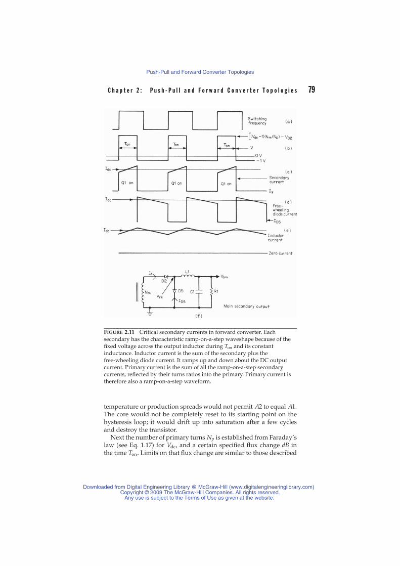
C h a p t e r 2 : P u s h - P u l l a n d F o r w a r d C o n v e r t e r T o p o l o g i e s 79
FIGURE 2.11 Critical secondary currents in forward converter. Eachsecondary has the characteristic ramp-on-a-step waveshape because of thefixed voltage across the output inductor during Ton and its constantinductance. Inductor current is the sum of the secondary plus thefree-wheeling diode current. It ramps up and down about the DC outputcurrent. Primary current is the sum of all the ramp-on-a-step secondarycurrents, reflected by their turns ratios into the primary. Primary current istherefore also a ramp-on-a-step waveform.
temperature or production spreads would not permit A2 to equal A1.The core would not be completely reset to its starting point on thehysteresis loop; it would drift up into saturation after a few cyclesand destroy the transistor.
Next the number of primary turns Np is established from Faraday’slaw (see Eq. 1.17) for Vdc, and a certain specified flux change dB inthe time Ton. Limits on that flux change are similar to those described
Downloaded from Digital Engineering Library @ McGraw-Hill (www.digitalengineeringlibrary.com)Copyright © 2009 The McGraw-Hill Companies. All rights reserved.
Any use is subject to the Terms of Use as given at the website.
Push-Pull and Forward Converter Topologies

80 S w i t c h i n g P o w e r S u p p l y D e s i g n
for the push-pull topology in Section 1.5.9 and will also be discussedlater.
Thus, in Eq. 2.25, Vdc, Ton, T , and Vd are specified, and Np is cal-culated from Faraday’s law. This fixes the number of main secondaryturns Nm needed to achieve the required main output voltage Vom.
2.3.3 Slave Output VoltagesThe slave output filters L2, C2 and L3, C3 average the width-modulated rectangular waveforms at their respective rectifier cath-odes. The waveform upper levels are [(Vdc − 1)(Ns1/Np)] − Vd3 and[(Vdc − 1)(Ns2/Np)] − Vd4, respectively. The low level voltages are onediode drop below ground. They are at the high level for the same max-imum Ton as is the main secondary, when the input DC input voltageis at the specified minimum Vdc. Again assuming that the forwardrectifier and free-wheeling diode drops equal Vd, the slave outputvoltages at low line Vdc are
Vs1 =[(
(Vdc − 1)Ns1
Np
)− Vd
]Ton
T(2.26)
Vs2 =[(
(Vdc − 1)Ns2
Np
)− Vd
]Ton
T(2.27)
By regulating Vom, the feedback loop keeps VdcTon constant, but thatsame product appears in Eqs. 2.26 and 2.27, and hence the slave out-puts remain constant as Vdc varies.
It can be seen from Eq. 2.24 and Figure 2.14 that the negative-feedback loop keeps the main output constant for either line or loadchanges by appropriately controlling Ton period, so that the sampledoutput is equal to the reference voltage Vref. This is not so obviousfor load changes, since load current does not appear directly in Eq.2.24, but it does appear indirectly. Load changes will change the “on”voltage of Q1 (assumed as 1 V heretofore) and the forward drop inthe rectifier diode. Although these changes are small, they will causesmall changes in the output voltage that will be sensed and correctedby the error amplifier by making a small change in Ton.
Moreover, as can be seen in Eqs. 2.26 and 2.27, any change in Tonwithout a corresponding change in Vdc will cause the slave output volt-ages to change. The slave output voltages also change with changes intheir own load currents. As those currents change, the rectifier forwarddrops also change, causing a change in the peak voltage at the inputto the LC averaging filter. So slave output voltages will change thepeak voltages to the averaging filters, with no corresponding changein Ton. Such changes in the slave output voltages as a result of loadchanges in the master and slave can be limited to within 5 to 8%.
Downloaded from Digital Engineering Library @ McGraw-Hill (www.digitalengineeringlibrary.com)Copyright © 2009 The McGraw-Hill Companies. All rights reserved.
Any use is subject to the Terms of Use as given at the website.
Push-Pull and Forward Converter Topologies

C h a p t e r 2 : P u s h - P u l l a n d F o r w a r d C o n v e r t e r T o p o l o g i e s 81
As discussed in Section 2.2.4, neither master nor slave output in-ductors can be permitted to go discontinuous at their minimum loadcurrents. This is ensured by choosing appropriately large output in-ductors, as will be described next.
The number of slave secondary turns Ns1, Ns2 are calculated fromEqs. 2.26 and 2.27, as all parameters there are either specified, or cal-culated from specified values. The parameters Vdc,T, and Vd are allspecified, and Ton is set at 0.8T/2 as discussed earlier; Np is calculatedfrom Faraday’s law (see Eq. 1.17) as described earlier.
2.3.4 Secondary Load, Free-Wheeling Diode,and Inductor Currents
Knowledge about the amplitudes and waveshapes of the various out-put currents is needed to select secondary and output inductor wiresizes and current ratings of the rectifiers and free-wheeling diodes.
As described for the buck regulator in Section 1.3.2, secondary cur-rent during the Q1 “on” time has the shape of an upward-slopingramp sitting on a step (see Figure 2.11c) because of the constant volt-age across the inductor during this time, with its input end positivewith respect to the output end.
When Q1 turns “off,” the input end of the inductor is negative withrespect to the output end and inductor current ramps downward.The free-wheeling diode, at the instant of turn “off,” picks up exactlythe inductor current that had been flowing just prior to turn “off.”That diode current then ramps downward (Figure 2.11d), as it is inseries with the inductor. Inductor current is the sum of the secondarycurrent when Q1 is “on” plus the free-wheeling diode current whenQ1 is “off,” and is shown in Figure 2.11e. Current at the center of theramp in any of Figure 2.11c, 2.11d, or 2.11e is equal to the DC outputcurrent.
2.3.5 Relations Between Primary Current,Output Power, and Input Voltage
Assume an efficiency of 80% of the total output power from all secon-daries to the DC power at the input voltage node. Then Po = 0.8Pinor Pin = 1.25Po . Now calculate Pin at minimum DC input voltageVdc ,which is Vdc times the average primary current at minimum DCinput.
All secondary currents have the waveshape of a ramp sitting ona step because all secondaries have output inductors. These ramp-on-a-step waveforms have a width of 0.8T/2 at minimum DC inputvoltage. All these secondary currents are reflected into the primaryby their turns ratios, and hence the primary current pulse is a single
Downloaded from Digital Engineering Library @ McGraw-Hill (www.digitalengineeringlibrary.com)Copyright © 2009 The McGraw-Hill Companies. All rights reserved.
Any use is subject to the Terms of Use as given at the website.
Push-Pull and Forward Converter Topologies

82 S w i t c h i n g P o w e r S u p p l y D e s i g n
ramp-on-a-step waveform of width 0.8T/2. There is only one suchpulse per period (see Figure 2.10) as this is a single-transistor circuit.The duty cycle of this primary pulse is then (0.8T/2)/T or 0.4.
Like the push-pull topology, this ramp-on-a-step can be approxi-mated by an equivalent flat-topped pulse Ipft of the same width andwhose amplitude is that at the center of the ramp. The average valueof this current is then 0.4Ipft. Then
Pin = 1.25Po = Vdc(0.4Ipft) or Ipft = 3.13Po
Vdc(2.28)
This is a valuable relation. It gives the equivalent peak flat-toppedprimary current pulse amplitude in terms of what is known at theoutset—the minimum DC input voltage and the total output power.This permits an immediate selection of a transistor with adequatecurrent rating and gain if it is a bipolar transistor, or with sufficientlylow “on” resistance if it is a MOSFET type.
For a forward converter, Eq. 2.28 shows Ipft has twice the amplitudeof that required in a push-pull topology (see Eq. 2.9) at the same outputpower and minimum DC input voltage.
This is obvious, because the push-pull has two pulses of currentor power per period as compared with a single pulse in the forwardconverter. From Eq. 2.25, if the number of secondary turns in the for-ward converter is chosen large enough, then the maximum “on” timeat minimum DC input voltage will not need to be greater than 80%of a half period. Then, as seen in Figure 2.10, the area A2 can alwaysequal A1 before the start of the next period. The core is then alwaysreset to the same point on its hysteresis loop within one cycle and cannever walk up into saturation.
The penalty paid for this guarantee that flux walking cannot occurin the forward converter is that the primary peak current is twice thatfor a push-pull at the same output power. Despite all the precautionsdescribed in Section 2.2.8, however, there is never complete certaintyin the push-pull that flux imbalance will not occur under unusualdynamic load or line conditions.
2.3.6 Maximum Off-Voltage Stressin Power Transistor
In the forward converter, with the number of turns on the reset wind-ing Nr equal to that on the power winding Np, maximum off-voltagestress on the power transistor is twice the maximum DC input volt-age plus a leakage inductance spike. These spikes and their originand minimization have been discussed in Section 2.2.11. Conservativedesign, even with all precautions to minimize leakage spikes, should
Downloaded from Digital Engineering Library @ McGraw-Hill (www.digitalengineeringlibrary.com)Copyright © 2009 The McGraw-Hill Companies. All rights reserved.
Any use is subject to the Terms of Use as given at the website.
Push-Pull and Forward Converter Topologies

C h a p t e r 2 : P u s h - P u l l a n d F o r w a r d C o n v e r t e r T o p o l o g i e s 83
assume they may be 30% above twice the maximum DC input volt-age. Maximum off-voltage stress is then the same as in the push-pulland is
Vms = 1.3(2Vdc) (2.29)
2.3.7 Practical Input Voltage/Output Power Limits
It was stated at the outset in Section 2.3.1 that the practical maximumoutput power limit for a forward converter whose maximum DC inputvoltage is under 60 V is 150 to 200 W. This is so because the peakprimary current as calculated from Eq. 2.28 becomes excessive, asthere is only a single pulse per period as compared with two in thepush-pull topology.
Thus consider a 200-W forward converter for the telephone industryin which the specified minimum and maximum input voltages are 38and 60 V, respectively. Peak primary current from Eq. 2.28 is Ipft =3.13Po/Vdc = 3.13(200)/38 = 16.5 A, and from Eq. 2.29, maximumoff-voltage stress is Vms = 2.6Vdc = 2.6 × 60 = 156 V.
To provide a safety margin, a device with at least a 200-V ratingwould be used to provide protection against input voltage transientsthat could drive the DC input above the maximum steady-state valueof 60 V.
Transistors with 200-V, 16-A ratings are available, but they all havedrawbacks as discussed in Section 2.2.13. Bipolar transistors are slow,and MOSFETs are easily fast enough but expensive. For such a 200-Wapplication, a push-pull version guaranteed to be free from flux imbal-ance would be preferable; with two pulses of current per period, peakcurrent would be only 8 A. With the resulting lower peak currentnoise spikes on the ground buses, the radio-frequency interference(RFI) would be considerably lower—a very important considerationfor a telephone industry power supply. Such a flux imbalance–freetopology is current mode, which is discussed later.
The forward converter topology, like the push-pull (discussed inSection 2.2.13), has the same difficulty in coping with maximum volt-age stress in an offline converter where the nominal AC input voltageis 120 ± 10%. At high line, the rectified DC input is 1.1 × 120 × 1.41 =186 V minus 2 V for the rectifier diode drops or 184 V. From Eq.2.29, the maximum voltage stress on the transistor in the “off” state isVms = 2.6 × 184 = 478 V.
At minimum AC input voltage, the rectified DC output is Vdc =(0.9 × 120 × 1.41) − 2 = 150 V, and from Eq. 2.28, the peak primarycurrent is Ipft = 3.13 × 22/150 = 4.17 A.
Downloaded from Digital Engineering Library @ McGraw-Hill (www.digitalengineeringlibrary.com)Copyright © 2009 The McGraw-Hill Companies. All rights reserved.
Any use is subject to the Terms of Use as given at the website.
Push-Pull and Forward Converter Topologies

84 S w i t c h i n g P o w e r S u p p l y D e s i g n
Thus, for a 200-W offline forward converter the problem is morethe 478-V maximum voltage stress than the 4.17-A peak primary cur-rent stress. As was seen in Section 2.2.13, when a 15% input tran-sient is taken into account, the peak off-voltage stress is 550 V. Witha bipolar transistor operating under Vcev conditions (reverse inputbias of −1 to −5 V at the instant of turn “off”), a voltage stress ofeven 550 V is not a serious restriction. Many devices have 650- to850-V Vcev ratings and high gain, low “on” drop, and high speed at4.17 A. But, as discussed in Section 2.2.13, there are preferable topolo-gies, discussed next, that subject the off transistor to only Vdc and nottwice Vdc.
2.3.8 Forward Converter With Unequal Powerand Reset Winding Turns
Heretofore it has been assumed that the numbers of turns on the powerwinding Np and the reset winding Nr are equal. Some advantagesresult if Nr is made less or greater than Np .
The number of primary power turns Np is always chosen by Fara-day’s law and will be discussed in Section 2.3.10.2. If Nr is chosen lessthan Np, the peak current required for a given output power is lessthan that calculated from Eq. 2.28, but the maximum Q1 off-voltagestress is greater than that calculated from Eq. 2.29. If Nr is chosen largerthan Np, the maximum Q1 off-voltage stress is less than that calcu-lated from Eq. 2.29, but the peak primary current for a given outputpower is greater than that calculated from Eq. 2.28. This can be seenfrom Figure 2.12 as follows. When Q1 turns “off,” polarities acrossNp and Nr reverse; the dot end of Nr goes negative and is caught atground by catch diode D1. Transformer T1 is now an autotransformer.There is a voltage Vdc across Nr and hence a voltage Np/Nr (Vdc) acrossNp . The core is set by the volt-second product by VdcTon during the“on” time and must be reset to its original place on the hysteresis loopby an equal volt-second product. That reset volt-second product isNp/Nr (Vdc)Tr .
When Nr equals Np, the reset voltage equals the set voltage, andthe reset time is equal to the set time (area A1 = area A2) as seen inFigure 2.12b. For Nr = Np, the maximum Q1 “on” time that occursat minimum DC input voltage is chosen as 0.8T/2 to ensure that thecore is reset before the start of the next period; Ton + Tr is then 0.8T.
Now if Nr is less than Np, the resetting voltage is larger than Vdc andconsequently Tr can be smaller (area A3 = area A4) as shown in Figure2.12c. With a shorter Tr , Ton can be longer than 0.8T/2, and Ton+Tr canstill be 0.8T so that the core is reset before the start of the next period.With a longer Ton, the peak current is smaller for the same averagecurrent and the same average output power. Thus in Figure 2.12c, a
Downloaded from Digital Engineering Library @ McGraw-Hill (www.digitalengineeringlibrary.com)Copyright © 2009 The McGraw-Hill Companies. All rights reserved.
Any use is subject to the Terms of Use as given at the website.
Push-Pull and Forward Converter Topologies
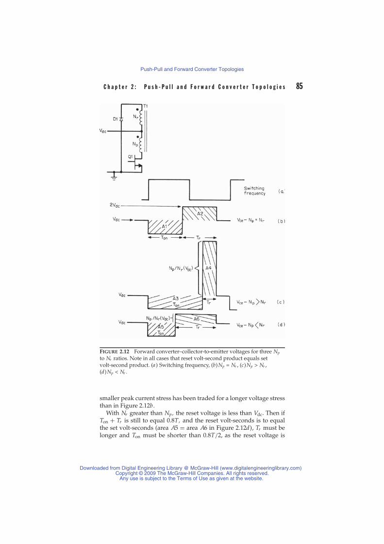
C h a p t e r 2 : P u s h - P u l l a n d F o r w a r d C o n v e r t e r T o p o l o g i e s 85
FIGURE 2.12 Forward converter–collector-to-emitter voltages for three Np
to Nr ratios. Note in all cases that reset volt-second product equals setvolt-second product. (a ) Switching frequency, (b)Np = Nr , (c)Np > Nr ,(d)Np < Nr .
smaller peak current stress has been traded for a longer voltage stressthan in Figure 2.12b.
With Nr greater than Np, the reset voltage is less than Vdc. Then ifTon + Tr is still to equal 0.8T, and the reset volt-seconds is to equalthe set volt-seconds (area A5 = area A6 in Figure 2.12d), Tr must belonger and Ton must be shorter than 0.8T/2, as the reset voltage is
Downloaded from Digital Engineering Library @ McGraw-Hill (www.digitalengineeringlibrary.com)Copyright © 2009 The McGraw-Hill Companies. All rights reserved.
Any use is subject to the Terms of Use as given at the website.
Push-Pull and Forward Converter Topologies

86 S w i t c h i n g P o w e r S u p p l y D e s i g n
less than the set voltage. With Ton less than 0.8T/2, the peak currentmust be higher for the same average current. Thus, in Figure 2.12d,a lesser voltage stress has been achieved at the cost of a higher peakcurrent for the same output power as in Figure 2.12b. This can be seenquantitatively as
Set Ton + Tr = 0.8T ; reset voltage = Vr = Np
NrVdc (2.30)
For “on” volt-seconds equal to reset volt-seconds,
VdcTon = Np
NrVdcTr (2.31)
Combining Eqs. 2.30 and 2.31,
Ton = 0.8T1 + Nr/Np
(2.32)
For 80% efficiency Pin = 1.25Po and Pin at Vdc = Vdc( Iav) =Vdc Ipft(Ton)/T or Ipft = 1.25( Po/Vdc)(T/Ton). Then from Eq. 2.32
Ipft = 1.56(
Po
Vdc
)(1 + Nr/Np) (2.33)
and the maximum Q1 off-voltage stress Vms—exclusive of the leakagespike—is the maximum DC input voltage Vdc plus the reset voltage(voltage across Np when the dot end of Nr is at ground). Thus
Vms = Vdc + Np
Nr(Vdc) = Vdc(1 + Np/Nr ) (2.34)
Values of Ipft and Vms calculated from Eqs. 2.33 and 2.34 are
Nr /Np Ipft(from Eq. 2.33) Vms(from Eq. 2.34)
0.6 2.50( Po/Vdc) 2.67 Vdc + leakage spike
0.8 2.81( Po/Vdc) 2.25 Vdc + ””
1.0 3.12( Po/Vdc) 2.00 Vdc + ””
1.2 3.43( Po/Vdc) 1.83 Vdc + ””
1.4 3.74( Po/Vdc) 1.71 Vdc + ””
1.6 4.06( Po/Vdc) 1.62 Vdc + ””
2.3.9 Forward Converter Magnetics2.3.9.1 First-Quadrant Operation OnlyThe transformer core in the forward converter operates in the firstquadrant of the hysteresis loop only. This can be seen in Figure 2.10.
Downloaded from Digital Engineering Library @ McGraw-Hill (www.digitalengineeringlibrary.com)Copyright © 2009 The McGraw-Hill Companies. All rights reserved.
Any use is subject to the Terms of Use as given at the website.
Push-Pull and Forward Converter Topologies

C h a p t e r 2 : P u s h - P u l l a n d F o r w a r d C o n v e r t e r T o p o l o g i e s 87
When Q1 is “on,” the dot end of T1 is positive with respect to theno-dot end, and the core is driven, say, in a positive direction on thehysteresis loop, and the magnetizing current ramps up linearly in themagnetizing inductance.
When Q1 turns “off,” stored current in the magnetizing inductancereverses the polarity of voltages on all windings. The dot end of Nrgoes negative until it is caught one diode drop below ground by catchdiode D1. Now the magnetizing current that is stored in the mag-netic core continues to flow. It simply transfers from Np, where it hadramped upward during the Q1 “on” time, into Nr where it ramps backto zero during the “off” time. It flows out of the no-dot end of Nr intothe positive end of the supply voltage Vdc, out of the negative end ofVdc, through D1, and back into Nr .
Since the dot end of Nr is positive with respect to its no-dot endduring the Q1 “off” time, the magnetizing current Id ramps linearlydownward, as can be seen in Figure 2.10. When it has ramped downto zero (at the end of area A2 in Figure 2.10), there is no longer anystored energy in the magnetizing inductance and nothing to hold thedot end of Nr below the D1 cathode. The voltage at the dot end of Nrstarts rising toward that at the D1 cathode. The voltage at the dot endof Nr starts rising toward Vdc, and that at the no-dot end of Np (Q1collector) starts falling from 2Vdc back down toward Vdc.
Thus operation on the hysteresis loop is centered about half thepeak magnetizing current (VdcTon/2Lm). Nothing ever reverses thedirection of the magnetizing current—it simply builds up linearly toa peak and relaxes back down linearly to zero.
This first-quadrant operation has some favorable and some un-favorable consequences. First, compared with a push-pull circuit, ithalves the available output power from a given core. This can be seenfrom Faraday’s law (see Eq. 1.17), which fixes the number of turns onthe primary.
By solving Faraday’s law for the number of primary turns, we getNp = E dt/AedB × 10−8. If dB in the forward converter is limited toan excursion from zero to some Bmax, instead of from –Bmax to +Bmaxas in a push-pull topology, the number of primary turns for the for-ward converter will be twice that in each half primary of a push-pulloperating from the same Vdc. Although the push-pull has two halfprimaries, each of which must support the same volt-second productas the forward converter primary, the push-pull provides two powerpulses per period as compared with one for the forward converter.The end result is that a core used in a forward converter can processonly half the output power available from the same core in a push-pullconfiguration.
However, the push-pull core at twice the output power will runsomewhat warmer, as its flux excursion is twice that of the forward
Downloaded from Digital Engineering Library @ McGraw-Hill (www.digitalengineeringlibrary.com)Copyright © 2009 The McGraw-Hill Companies. All rights reserved.
Any use is subject to the Terms of Use as given at the website.
Push-Pull and Forward Converter Topologies

88 S w i t c h i n g P o w e r S u p p l y D e s i g n
converter. Since core losses are proportional to the area of the hys-teresis loop traversed, the push-pull core losses are twice that of theforward converter.
Yet total copper losses in both half primaries of a push-pull areno greater than that of a forward converter of half the output power,because the rms current in each push-pull half primary is equal to thatin the forward converter primary. Since the number of turns in eachpush-pull half primary is half that of the forward converter primaryof half the output power, they also have half the resistance. Thus totalcopper loss in a forward converter is equal to the total loss of the twohalf primaries in a push-pull of twice the output power.
2.3.9.2 Core Gapping in a Forward ConverterIn Figure 2.3, we see the hysteresis loop of a ferrite core with no airgap. We see that at zero magnetizing force (0 Oe) there is a residualmagnetic flux density of about ± 1000 G. This residual flux is referredto as remanence.
In a forward converter, if the core started at 0 Oe and hence at1000 G, the maximum flux change in dB possible before the core isdriven up into the curved part of the hysteresis loop is about 1000 G.It is desirable to stay off the curved part of the hysteresis loop, andhence the forward converter core with no air gap is restricted to amaximum dB of 1000 G. As shown earlier, the number of primary turnsis inversely proportional to dB. Such a relatively small dB requires arelatively large number of primary turns. A large number of primaryturns requires small wire size and hence decreases the current andpower available from the transformer.
By introducing an air gap in the core, the hysteresis loop is tilted asshown in Figure 2.5, and magnetic remanence is reduced significantly.The hysteresis loop tilts over but still crosses the H (coercive force) axiswith zero flux density at the same point. Coercive force for ferrites isseen to be about 0.2 Oe in Figure 2.3. An air gap of 2 to 4 mils willreduce remanence to about 200 G for most cores used at 200 to 500 Wof output power. With remanence of 200 G, the dB before the coreenters the curved part of the hysteresis loop is now about 1800 G, andfewer turns are permissible.
However, a penalty is paid in introducing an air gap. Figure 2.5shows the slope of the hysteresis loop tilted over. The slope is dB/dHor core permeability, which has been decreased by adding the gap.Decreasing permeability decreases magnetizing inductance and in-creases magnetizing current (Im = VdcTon/Lm). Magnetizing currentcontributes no output power to the load; it simply moves the operatingpoint of the core around the hysteresis loop and contributes significantcopper loss if it exceeds 10% of the primary load current.
Downloaded from Digital Engineering Library @ McGraw-Hill (www.digitalengineeringlibrary.com)Copyright © 2009 The McGraw-Hill Companies. All rights reserved.
Any use is subject to the Terms of Use as given at the website.
Push-Pull and Forward Converter Topologies

C h a p t e r 2 : P u s h - P u l l a n d F o r w a r d C o n v e r t e r T o p o l o g i e s 89
2.3.9.3 Magnetizing Inductance with Gapped CoreMagnetizing inductance with a gapped core can be calculated as fol-lows. Voltage across the magnetizing inductance is LmdIm/dt and fromFaraday’s law:
Vdc = LmdIm
dt= Np AedB
dt10−8 or Lm = Np AedB
dIm10−8 (2.35)
where Lm = magnetizing inductance, HNp = number of primary turnsAe = core area, cm2
dB = core flux change, GdIm = change in magnetizing current, A
A fundamental law in magnetics is Ampere’s law:∫H · dl = 0.4πNI
This states that if a line is drawn encircling a number of ampere turnsNI, the dot product H · dl along that line is equal to 0.4πNI. If the lineis taken through the core parallel to the magnetic flux lines and acrossthe gap, since H is uniform at a value Hi within the core and uniformat a value Ha within the gap, then
Hili + Hala = 0.4πNIm (2.36)
where Hi = magnetic field intensity in iron (ferrite), Oeli = length of iron path, cmHa = magnetic field intensity in air gap, Oela = length of air gap, cmIm = magnetizing current, A
However, Hi = Bi/u, where Bi is the magnetic flux density in ironand u is the iron permeability; Ha = Ba as the permeability of air is 1;and Ba = Bi (flux density in iron = flux density in air) if fringing fluxaround the air gap is ignored. Then Eq. 2.36 can be written as
Bi
uli + Bi la = 0.4πNp Im or Bi = 0.4πNIm
la + li/u(2.37)
Then dB/dIm = 0.4πN/(la + li/u), and substituting this into Eq. 2.35:
Lm = 0.4π(Np)2 Ae × 10−9
la + li/u(2.38)
Downloaded from Digital Engineering Library @ McGraw-Hill (www.digitalengineeringlibrary.com)Copyright © 2009 The McGraw-Hill Companies. All rights reserved.
Any use is subject to the Terms of Use as given at the website.
Push-Pull and Forward Converter Topologies

90 S w i t c h i n g P o w e r S u p p l y D e s i g n
Thus, introducing an air gap of length la to a core of iron path lengthli reduces the magnetizing inductance in the ratio of
Lm (with gap)
Lm (without gap)= li/u
la + li/u(2.39)
It is instructive to consider a specific example. Take an internationalstandard core such as the Ferroxcube 783E608-3C8. It has a magneticpath length of 9.7 cm and an effective permeability of 2300. Then if a4-mil (= 0.0102-cm) gap were introduced into the magnetic path, fromEq. 2.39:
Lm (with gap) = 9.7/23000.0102 + 9.7/2300
Lm (without gap)
= 0.29Lm (without gap)
A useful way of looking at a gapped core is to examine the denom-inator in Eq. 2.38. In most cases, u is so high that the term li/u issmall compared with the air gap la , and the inductance is determinedprimarily by the length of the air gap.
2.3.10 Power Transformer Design Relations2.3.10.1 Core SelectionAs discussed in Section 2.2.9.1 on core selection for a push-pull trans-former, the amount of power available from a core for a forward con-verter transformer is related to the same parameters—peak flux den-sity, core iron and window areas, frequency, and coil current densityin circular mils per rms ampere.
In Chapter 7, an equation will be derived giving the amount ofavailable output power as a function of these parameters. This equa-tion will be converted to a chart that permits selection of core size andoperating frequency at a glance.
For the present, it is assumed that a core has been selected and thatits iron and window areas are known.
2.3.10.2 Primary Turns CalculationThe number of primary turns is calculated from Faraday’s law as givenin Eq. 2.7. From Section 2.3.9.2, we see that in the forward converterwith a gapped core, flux density moves from about 200 G to somehigher value Bmax.
In the push-pull topology as discussed in Section 2.2.9.4, this peakvalue will be set at 1600 G (for ferrites at low frequencies, where corelosses are not a limiting factor). This avoids the problem of a muchlarger and more dangerous flux swing due to rapid changes in DC
Downloaded from Digital Engineering Library @ McGraw-Hill (www.digitalengineeringlibrary.com)Copyright © 2009 The McGraw-Hill Companies. All rights reserved.
Any use is subject to the Terms of Use as given at the website.
Push-Pull and Forward Converter Topologies

C h a p t e r 2 : P u s h - P u l l a n d F o r w a r d C o n v e r t e r T o p o l o g i e s 91
input voltage or load currents. Such rapid changes are not imme-diately compensated because the limited error-amplifier bandwidthcan’t correct the power transistor “on” time fast enough.
During this error-amplifier delay, the peak flux density can exceedthe calculated normal steady-state value for a number of cycles. Thiscan be tolerated if the normal peak flux density in the absence of a lineor load transient is set to the low value of 1600 G. As discussed earlier,the excursion from approximately zero to 1600 G will take place in80% of a half period to ensure that the core can be reset before the startof the next period (see Figure 2.12b).
Thus, the number of primary turns is set by Faraday’s law at
Np = (Vdc − 1)(0.8T/2) × 10+8
AedB(2.40)
where Vdc = minimum DC input, VT = operating period, sAe = iron area, cm2
dB = change in flux density, G
2.3.10.3 Secondary Turns CalculationSecondary turns are calculated from Eqs. 2.25 to 2.27. In those rela-tions, all values except the secondary turns are specified or alreadycalculated. Thus (see Figure 2.10):
Vdc = minimum DC input, V
Ton = maximum “on” time, s(= 0.8T/2)
Nm, Ns1, Ns2 = numbers of main and slave turns
Np = number of primary turns
Vd = rectifier forward drop
If the main output produces 5 V at high current as is often the case,a Schottky diode with forward drop of about 0.5 V is typically used.The slaves usually have higher output voltages that require the use offast-recovery diodes with higher reverse-voltage ratings. Such diodeshave forward drops of about 1.0 V over a large range of current.
2.3.10.4 Primary rms Current and Wire Size SelectionPrimary equivalent flat-topped current is given by Eq. 2.28. That cur-rent flows for a maximum of 80% of a half period per period, so its max-imum duty cycle is 0.4. Recalling that the rms value of a flat-topped
Downloaded from Digital Engineering Library @ McGraw-Hill (www.digitalengineeringlibrary.com)Copyright © 2009 The McGraw-Hill Companies. All rights reserved.
Any use is subject to the Terms of Use as given at the website.
Push-Pull and Forward Converter Topologies

92 S w i t c h i n g P o w e r S u p p l y D e s i g n
pulse of amplitude Ip is Irms = Ip√
Ton/T, the rms primary current is
Irms (primary) = 3.12Po
Vdc
√0.4
= 1.97Po
Vdc
(2.41)
If the wire size is chosen on the basis of 500 circular mils per rmsampere, the required number of circular mils is
Circular mils needed = 500 × 1.97Po
Vdc
= 985Po
Vdc
(2.42)
2.3.10.5 Secondary rms Current and Wire Size SelectionIt is seen in Figure 2.11 that the secondary current has the characteris-tic shape of a ramp on a step. The pulse amplitude at the center of theramp is equal to the average DC output current. Thus, the equivalentflat-topped secondary current pulse at Vdc (when its width is a maxi-mum) has amplitude Idc, width 0.8T/2, and duty cycle (0.8T/2)/T or0.4. Then
Irms(secondary) = Idc√
0.4
= 0.632Idc(2.43)
and at 500 circular mils per rms ampere, the required number of cir-cular mils for each secondary is
Circular mils needed = 500 × 0.632Idc
= 316Idc(2.44)
2.3.10.6 Reset Winding rms Current and Wire Size SelectionThe reset winding carries only magnetizing current, as can be seen bythe dots in Figure 2.10. When Q1 is “on,” diode D1 is reverse-biased,and no current flows in the reset winding. But magnetizing currentbuilds up linearly in the power winding Np. When Q1 turns “off,”that magnetizing current must continue to flow. When Q1 currentceases, the current in the magnetizing inductance reverses all windingvoltage polarities. When D1 clamps the dot end of Nr to ground, themagnetizing current transfers from Np to Nr and continues flowingthrough the DC input voltage source Vdc, through D1, and back intoNr . Since the no-dot end of Nr is positive with respect to the dotend, the magnetizing current ramps downward to zero as seen inFigure 2.10.
Downloaded from Digital Engineering Library @ McGraw-Hill (www.digitalengineeringlibrary.com)Copyright © 2009 The McGraw-Hill Companies. All rights reserved.
Any use is subject to the Terms of Use as given at the website.
Push-Pull and Forward Converter Topologies

C h a p t e r 2 : P u s h - P u l l a n d F o r w a r d C o n v e r t e r T o p o l o g i e s 93
The waveshape of this Nr current is the same as that of the mag-netizing current that ramped upward when Q1 was “on,” but it isreversed from left to right. Thus the peak of this triangle of current isIp(magnetizing) = VdcTon/Lmg, where Lmg is the magnetizing inductancewith an air gap as calculated from Eq. 2.39. The inductance withoutthe gap is calculated from the ferrite catalog value of Al, the induc-tance per 1000 turns. Since inductance is proportional to the square ofthe number of turns, inductance for n turns is Ln = Al (n/1000)2. Theduration of this current triangle is 0.8T/2 (the time required for thecore to reset), and it comes at a duty cycle of 0.4.
It is known that the rms value of a repeating triangle waveform(no spacing between successive triangles) of peak amplitude Ip isIrms = Ip
√3. But this triangle comes at a duty cycle of 0.4, and hence
its rms value is
Irms = VdcTon
Lmg
√0.4√3
= 0.365VdcTon
Lmg
and at 500 circular mils per rms ampere, the required number of cir-cular mils for the reset winding is
Circular mils required = 500 × 0.365VdcTon
Lmg(2.45)
Most frequently, the magnetizing current is so small that the resetwinding wire can be No. 30 AWG or smaller.
2.3.11 Output Filter Design RelationsThe output filters L1C1, L2C2, and L3C3 average the voltage wave-form at the rectifier cathodes. The inductor is selected to operate incontinuous mode (see Section 1.3.6) at the minimum DC output cur-rent. The capacitor is selected to yield a specified minimum outputripple voltage.
2.3.11.1 Output Inductor DesignRecall from Section 1.3.6 that discontinuous mode condition occurswhen the inductor current ramp drops to zero (see Figure 2.10). Sincethe DC output current is the value at the center of the ramp, discon-tinuous mode occurs at a minimum current Idc equal to half the rampamplitude dI as can be seen in Figure 2.10.
Downloaded from Digital Engineering Library @ McGraw-Hill (www.digitalengineeringlibrary.com)Copyright © 2009 The McGraw-Hill Companies. All rights reserved.
Any use is subject to the Terms of Use as given at the website.
Push-Pull and Forward Converter Topologies
94 S w i t c h i n g P o w e r S u p p l y D e s i g n
Now referring to Figure 2.11,
dI = 2Idc = (Vrk − Vo )Ton
L1or L1 = (Vrk − Vo (Ton)
2Idc
But Vo = VrkTon/T. Then
L1 =(
Vo TTon
− Vo
)Ton
2Idc
= Vo (T/Ton − 1)/Ton
2Idc
But Ton = 0.8T/2. Then
L1 = 0.3Vo TIdc
(2.46)
and if the minimum DC current Idc is one-tenth the nominal outputcurrent Ion, then
L1 = 3Vo TIon
(2.47)
2.3.11.2 Output Capacitor DesignIt was seen in Section 1.3.7 that the output ripple is almost completelydetermined by the equivalent series resistance Ro of the filter capacitor.The peak-to-peak ripple amplitude is Vor = Ro dI, where dI is the peak-to-peak ripple current amplitude chosen by the selection of the rippleinductor as discussed earlier. Assuming that the average value of RoCofor aluminum electrolytic capacitors over a large range of voltage andcapacitance ratings is given by RoCo = 65 × 10−6 as in Section 1.3.7,then
Co = 65 × 10−6/Ro
= 65 × 10−6 dIVor
(2.48)
where dI is in amperes and Vor is in volts for Co in farads.
2.4 Double-Ended ForwardConverter Topology2.4.1 Basic OperationDouble-ended forward converter topology is shown in Figure 2.13.Although it has two transistors rather than one compared with thesingle-ended forward converter of Figure 2.10, it has a very significant
Downloaded from Digital Engineering Library @ McGraw-Hill (www.digitalengineeringlibrary.com)Copyright © 2009 The McGraw-Hill Companies. All rights reserved.
Any use is subject to the Terms of Use as given at the website.
Push-Pull and Forward Converter Topologies
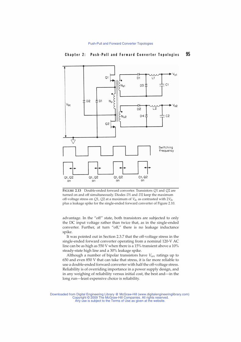
C h a p t e r 2 : P u s h - P u l l a n d F o r w a r d C o n v e r t e r T o p o l o g i e s 95
FIGURE 2.13 Double-ended forward converter. Transistors Q1 and Q2 areturned on and off simultaneously. Diodes D1 and D2 keep the maximumoff-voltage stress on Q1, Q2 at a maximum of Vdc as contrasted with 2Vdc
plus a leakage spike for the single-ended forward converter of Figure 2.10.
advantage. In the “off” state, both transistors are subjected to onlythe DC input voltage rather than twice that, as in the single-endedconverter. Further, at turn “off,” there is no leakage inductancespike.
It was pointed out in Section 2.3.7 that the off-voltage stress in thesingle-ended forward converter operating from a nominal 120-V ACline can be as high as 550 V when there is a 15% transient above a 10%steady-state high line and a 30% leakage spike.
Although a number of bipolar transistors have Vcev ratings up to650 and even 850 V that can take that stress, it is far more reliable touse a double-ended forward converter with half the off-voltage stress.Reliability is of overriding importance in a power supply design, andin any weighing of reliability versus initial cost, the best and—in thelong run—least expensive choice is reliability.
Downloaded from Digital Engineering Library @ McGraw-Hill (www.digitalengineeringlibrary.com)Copyright © 2009 The McGraw-Hill Companies. All rights reserved.
Any use is subject to the Terms of Use as given at the website.
Push-Pull and Forward Converter Topologies

96 S w i t c h i n g P o w e r S u p p l y D e s i g n
Further, for power supplies to be used in the European marketwhere the AC voltage is 220 V (rectified DC voltage is nominally about308 V), the single-ended forward converter is not usable at all becauseof the excessive voltage stress on the off transistor (see Eq. 2.29). Thedouble-ended forward converter, the half bridge, and the full bridge(to be discussed in Chapter 3) are the only choices for equipment tobe used in the European market.
The double-ended forward converter works as follows. In Figure2.13, Q1 and Q2 are in series with the transformer primary. These tran-sistors are turned on and off simultaneously. When they are “on,” allprimary and secondary dot ends are positive, and power is deliveredto the loads. When they turn “off,” current stored in the T1 magne-tizing inductance reverses the voltage polarity of all windings. Thenegative-going dot end of Np is caught at ground by diode D1, andthe positive-going no-dot end of Np is caught at Vdc by diode D2.
Thus the emitter of Q1 can never be more than Vdc below its col-lector, and the collector of Q2 can never be more than Vdc above itsemitter. Leakage inductance spikes are clamped so that the maximumvoltage stress on either transistor can never be more than the maxi-mum DC input voltage.
The further significant advantage is that there is no leakage induc-tance energy to be dissipated. Any energy stored in the leakage in-ductance is not lost by dissipation in some resistive element or in thepower transistors. Instead, energy stored in the leakage inductanceduring the “on” time is fed back into Vdc via D1 and D2 when thetransistors turn “off.” The leakage inductance current flows out of theno-dot end of Np, through D2, into the positive end of Vdc, out of itsnegative end, and up through D1 back into the dot end of Np.
Examination of Figure 2.13 reveals that the core is always reset ina time equal to the “on” time. The reverse polarity voltage across Npwhen the transistors are “off” is equal to the forward polarity voltageacross it when the transistors are “on.” Thus the core will always befully reset with a 20% safety margin before the start of a succeedinghalf cycle if the maximum “on” time is no greater than 80% of a halfperiod. This is accomplished by choosing secondary turns so that thepeak secondary voltage at minimum Vdc times the maximum dutycycle of 0.4 equals the desired output voltage (see Eq. 2.25).
2.4.1.1 Practical Output Power LimitsIt should be noted that this topology still yields only one power pulseper period, just like the single-ended forward converter. Thus thepower available from a specific core is pretty much the same for eitherthe single- or double-ended configuration. As noted in Section 2.3.10.6,the reset winding in the single-ended circuit carries only magnetizingcurrent during the power transistor “off” time. Since that current is
Downloaded from Digital Engineering Library @ McGraw-Hill (www.digitalengineeringlibrary.com)Copyright © 2009 The McGraw-Hill Companies. All rights reserved.
Any use is subject to the Terms of Use as given at the website.
Push-Pull and Forward Converter Topologies

C h a p t e r 2 : P u s h - P u l l a n d F o r w a r d C o n v e r t e r T o p o l o g i e s 97
small, the reset winding can be wound with very small wire. Thus, theabsence of a reset winding in the double-ended circuit does not permitsignificantly larger power winding wire size and output power froma given core.
Because the maximum off transistor voltage stress cannot be greaterthan the maximum DC input voltage, however, the 200-W practicalpower limit for the single-ended forward converter discussed in Sec-tion 2.3.7 does not hold for the double-ended forward converter. Withthe reduced voltage stress, output powers of 400 to 500 W are obtain-able, and transistors with the required voltage and current capabilityand adequate gain are available at low price.
Consider a double-ended forward converter operating from a nom-inal 120-V AC line with ± 10% tolerance and ± 15% allowance fortransients on top of that. The maximum rectified DC voltage is 1.41 ×120 × 1.1 × 1.15 = 214 V, and the minimum rectified DC voltage is1.41 × 120 ÷ 1.1÷1.15 = 134 V, and equivalent flat-topped primary cur-rent from Eq. 2.28 is Ipft = 3.13Po/Vdc, and for Po = 400 W, Ipft = 9.6 A.This requirement can be satisfied quite easily, because both bipolar andMOSFET transistors with adequately high gain are available at lowcost.
A double-ended forward converter with a voltage doubler fromthe 120-V AC line would be a better alternative (see Figure 3.1). Thiswould double the voltage stress to 428 V but would halve the peakcurrent to 4.8 A. With 4.8 A of primary current, RFI problems would beless severe. A bipolar transistor with a 400-V Vceo rating could tolerate428 V easily, with –1- to –5-V reverse bias at the instant of turn “off”(Vcev rating).
2.4.2 Design Relations andTransformer Design
2.4.2.1 Core Selection—Primary Turns and Wire SizeThe transformer design for the double-ended forward converter pro-ceeds exactly as for the single-ended converter. A core is selected fromthe aforementioned selection charts (to be presented in Chapter 7 onmagnetics) for the required output power and operating frequency.
The number of primary turns is chosen from Faraday’s law as inEq. 2.40. There the minimum primary voltage is (Vdc − 2) as thereare two transistors rather than one in series with the primary—butthe transistor drops are insignificant since Vdc is usually 134 V (120 VAC). Maximum “on” time should be set at 0.8T/2 and dB at 1600 Gup to 50 kHz, or higher if not limited by core losses.
As mentioned for frequencies from 100 to 300 kHz, peak flux densitymay have to be set from about 1400 to 800 G, as core losses increasewith frequency. But the exact peak flux density chosen depends on
Downloaded from Digital Engineering Library @ McGraw-Hill (www.digitalengineeringlibrary.com)Copyright © 2009 The McGraw-Hill Companies. All rights reserved.
Any use is subject to the Terms of Use as given at the website.
Push-Pull and Forward Converter Topologies

98 S w i t c h i n g P o w e r S u p p l y D e s i g n
whether the newer, lower-loss materials are available. It also dependsto some extent on transformer size—smaller cores can generally oper-ate at higher flux density, because they have a larger ratio of radiatingsurface area to volume and hence can get rid of the heat they generate(which is proportional to volume) more easily.
Since there is only one current or power pulse per period, as inthe single-ended forward converter, the primary current for a givenoutput power and minimum DC input voltage is given by Eq. 2.28,and the primary wire size is chosen from Eq. 2.42.
2.4.2.2 Secondary Turns and Wire SizeSecondary turns are chosen exactly as in Sections 2.3.2 and 2.3.3 fromEqs. 2.25 to 2.27. Wire sizes are calculated as in Section 2.3.10.5 fromEq. 2.44.
2.4.2.3 Output Filter DesignThe output inductor and capacitor magnitudes are calculated exactlyas in Section 2.3.11 from Eqs. 2.46 to 2.48.
2.5 Interleaved Forward Converter Topology2.5.1 Basic Operation—Merits, Drawbacks,
and Output Power LimitsThis topology is simply two identical single-ended forward convertersoperating on alternate half cycles with their secondary currents addingthrough rectifying “on” diodes. The topology is shown in Figure 2.14.
The advantage, of course, is that now there are two power pulsesper period, as seen in Figure 2.14, reducing the ripple current; alsoeach converter supplies only half the total output power.
Equivalent flat-topped peak transistor current is derived fromEq. 2.28 as Ipft = 3.13 Pot/2Vdc where Pot is the total output power.This transistor current is half that of a single forward converter at thesame total output power. Thus the expense of two transistors is offsetby the lower peak current rating and lower cost than that of the highercurrent rating device.
Looking at it another way, two transistors of the same current ratingused at the same peak current as one single-ended converter at a givenoutput power in an interleaved converter would yield twice the outputpower of the single converter.
Also, since the intensity of EMI generated is proportional to the peakcurrent, not to the number of current pulses, an interleaved converterof the same total output power as a single forward converter willgenerate less EMI.
Downloaded from Digital Engineering Library @ McGraw-Hill (www.digitalengineeringlibrary.com)Copyright © 2009 The McGraw-Hill Companies. All rights reserved.
Any use is subject to the Terms of Use as given at the website.
Push-Pull and Forward Converter Topologies
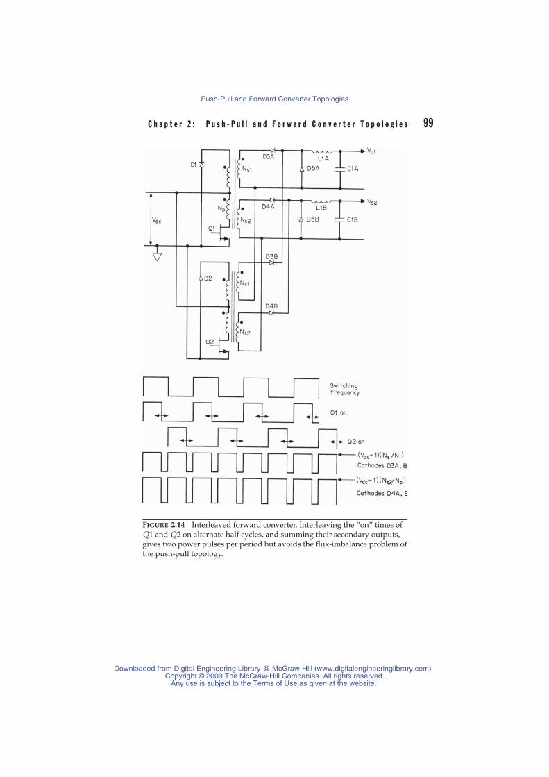
C h a p t e r 2 : P u s h - P u l l a n d F o r w a r d C o n v e r t e r T o p o l o g i e s 99
FIGURE 2.14 Interleaved forward converter. Interleaving the “on” times ofQ1 and Q2 on alternate half cycles, and summing their secondary outputs,gives two power pulses per period but avoids the flux-imbalance problem ofthe push-pull topology.
Downloaded from Digital Engineering Library @ McGraw-Hill (www.digitalengineeringlibrary.com)Copyright © 2009 The McGraw-Hill Companies. All rights reserved.
Any use is subject to the Terms of Use as given at the website.
Push-Pull and Forward Converter Topologies

100 S w i t c h i n g P o w e r S u p p l y D e s i g n
If this topology is compared to a push-pull, it might be thought thatthe push-pull is preferable. Although both are two-transistor circuits,the two transformers in the interleaved forward converter are prob-ably more expensive and occupy more space than a single large onein a push-pull circuit. But there is the ever-present uncertainty thatthe flux imbalance problem in the push-pull could appear under oddtransient line and load conditions. The certainty that there is no fluximbalance in the interleaved forward converter is probably the bestargument for its use.
There is one special, although not frequent, case where the inter-leaved forward converter is a much more desirable choice than a sin-gle forward converter of the same output power. This occurs whena DC output voltage is high—over about 200 V. In a single forwardconverter the peak reverse voltage experienced by the output free-wheeling diodes (D5Aor D5B) is twice that for an interleaved forwardconverter as the duty cycle in the latter is twice that in the former.
This is no problem when output voltages are low, as can be seenin Eq. 2.25. Transformer secondary turns are always selected (for thesingle forward converter) so that at minimum DC input, when thesecondary voltage is at its minimum, the duty cycle Ton/T need notbe more than 0.4 to yield the desired output voltage. Then for a DCoutput of 200 V, the peak reverse voltage experienced by the free-wheeling diode is 500 V. At the instant of power transistor turn “on,”the free-wheeling diode has been carrying a large forward current andwill suddenly be subjected to reverse voltage. If the diode has slowreverse recovery time, it will draw a large reverse current for a shorttime at 500-V reverse voltage and run dangerously hot.
Diodes with larger reverse voltage ratings generally have slowerrecovery times and can be a serious problem. The interleaved forwardconverter runs at twice the duty cycle and, for a 200 V-DC output,subjects the free-wheeling diode to only 250 V. This permits a lowervoltage, faster-recovery diode with considerably lower dissipation.
2.5.2 Transformer Design Relations2.5.2.1 Core SelectionThe core for the two transformers will be selected from the aforemen-tioned charts, to be presented in Chapter 7, but it will be chosen forhalf the total power output that each transformer must supply.
2.5.2.2 Primary Turns and Wire SizeThe number of primary turns in the interleaved forward converteris still given by Eq. 2.40, as each converter’s “on” time will still be0.8T/2 at minimum DC input. The core iron area Ae will be read from
Downloaded from Digital Engineering Library @ McGraw-Hill (www.digitalengineeringlibrary.com)Copyright © 2009 The McGraw-Hill Companies. All rights reserved.
Any use is subject to the Terms of Use as given at the website.
Push-Pull and Forward Converter Topologies

C h a p t e r 2 : P u s h - P u l l a n d F o r w a r d C o n v e r t e r T o p o l o g i e s 101
the catalogs for the selected core. Primary wire size will be chosenfrom Eq. 2.42 at half the total output power.
2.5.2.3 Secondary Turns and Wire SizeThe number of secondary turns will be chosen from Eqs. 2.26 and 2.27,but therein the duty cycle will be 0.8 as there are two voltage pulses,each of duration 0.8T/2 at Vdc. Wire size will still be chosen from Eq.2.44, where Idc is the actual DC output current that each secondarycarries at a maximum duty cycle of 0.4.
2.5.3 Output Filter Design2.5.3.1 Output Inductor DesignThe output inductor sees two current pulses per period, exactly likethe output inductor in the push-pull topology. These pulses have thesame width, amplitude, and duty cycle as the push-pull inductor atthe same DC output current. Hence the magnitude of the inductanceis calculated from Eq. 2.20 as for the push-pull inductor.
2.5.3.2 Output Capacitor DesignSimilarly, the output capacitor “doesn’t know” whether it is filteringa full-wave secondary waveform from a push-pull topology or froman interleaved forward converter. Thus for the same inductor cur-rent ramp amplitude and permissible output ripple as the push-pullcircuit, the capacitor is selected from Eq. 2.22.
Reference1. K. Billings, Switchmode Power Supply Handbook, New York: McGraw-Hill, 1990.
Downloaded from Digital Engineering Library @ McGraw-Hill (www.digitalengineeringlibrary.com)Copyright © 2009 The McGraw-Hill Companies. All rights reserved.
Any use is subject to the Terms of Use as given at the website.
Push-Pull and Forward Converter Topologies

Downloaded from Digital Engineering Library @ McGraw-Hill (www.digitalengineeringlibrary.com)Copyright © 2009 The McGraw-Hill Companies. All rights reserved.
Any use is subject to the Terms of Use as given at the website.
Push-Pull and Forward Converter Topologies
C H A P T E R 3Half- and Full-BridgeConverter Topologies
3.1 IntroductionHalf-bridge and full-bridge topologies stress their transistors to a volt-age equal to the DC input voltage not to twice this value, as do thepush-pull, single-ended, and interleaved forward converter topolo-gies. Thus the bridge topologies are used mainly in offline converterswhere supply voltage would be more than the switching transistorscould safely tolerate. Bridge topologies are almost always used wherethe normal AC input voltage is 220 V or higher, and frequently evenfor 120-V AC inputs.
An additional valuable feature of the bridge topologies is thatprimary leakage inductance spikes (Figures 2.1 and 2.10) are easilyclamped to the DC supply bus and the energy stored in the leakageinductance is returned to the input instead of having to be dissipatedin a resistive snubber element.
3.2 Half-Bridge Converter Topology3.2.1 Basic OperationHalf-bridge converter topology is shown in Figure 3.1. Its major ad-vantage is that, like the double-ended forward converter, it subjectsthe “off” transistor to only Vdc and not twice that value. Thus it iswidely used in equipment intended for the European market, wherethe AC input voltage is 220 V.
First consider the input rectifier and filter in Figure 3.1. It is useduniversally when the equipment is to work from either 120-V ACAmerican power or 220-V AC European power. The circuit alwaysyields roughly 320-V rectified DC voltage, whether the input is 120 or
103Downloaded from Digital Engineering Library @ McGraw-Hill (www.digitalengineeringlibrary.com)
Copyright © 2009 The McGraw-Hill Companies. All rights reserved.Any use is subject to the Terms of Use as given at the website.
Source: Switching Power Supply Design
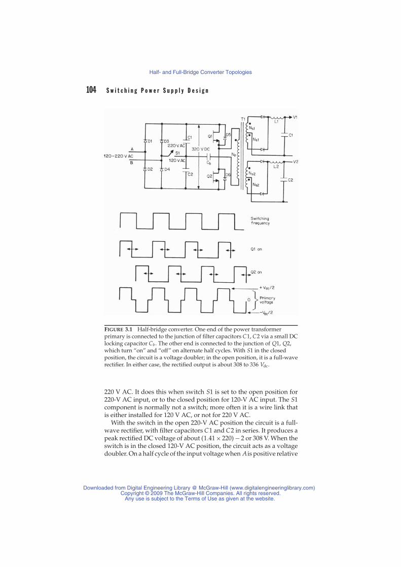
104 S w i t c h i n g P o w e r S u p p l y D e s i g n
FIGURE 3.1 Half-bridge converter. One end of the power transformerprimary is connected to the junction of filter capacitors C1, C2 via a small DClocking capacitor Cb . The other end is connected to the junction of Q1, Q2,which turn “on” and “off” on alternate half cycles. With S1 in the closedposition, the circuit is a voltage doubler; in the open position, it is a full-waverectifier. In either case, the rectified output is about 308 to 336 Vdc.
220 V AC. It does this when switch S1 is set to the open position for220-V AC input, or to the closed position for 120-V AC input. The S1component is normally not a switch; more often it is a wire link thatis either installed for 120 V AC, or not for 220 V AC.
With the switch in the open 220-V AC position the circuit is a full-wave rectifier, with filter capacitors C1 and C2 in series. It produces apeak rectified DC voltage of about (1.41 × 220) − 2 or 308 V. When theswitch is in the closed 120-V AC position, the circuit acts as a voltagedoubler. On a half cycle of the input voltage when Ais positive relative
Downloaded from Digital Engineering Library @ McGraw-Hill (www.digitalengineeringlibrary.com)Copyright © 2009 The McGraw-Hill Companies. All rights reserved.
Any use is subject to the Terms of Use as given at the website.
Half- and Full-Bridge Converter Topologies

C h a p t e r 3 : H a l f - a n d F u l l - B r i d g e C o n v e r t e r T o p o l o g i e s 105
to B, C1 is charged positively via D1 to a peak of (1.41 × 120) − 1 or168 V. On a half cycle when A is negative with respect to B, capacitorC2 is charged positively via D2 to 168 V. The total voltage across C1and C2 in series is then 336 V. It can be seen in Figure 3.1 that witheither transistor “on,” the “off” transistor is subjected to the maximumDC input voltage and not twice that value.
Since the topology subjects the “off” transistor to only Vdc and not2Vdc, there are many inexpensive bipolar and MOSFET transistorsthat can support the nominal 336 DC V plus 15% upper maximum of386 V. Thus the equipment can be used with either 120- or 220-V ACline inputs by making a simple switch or linkage change.
After Pressman An automatic line voltage sensing and switching cir-cuit that drives a relay or other device in the position of S1 is sometimesimplemented. The added cost and circuit complexity is offset by making theswitching action transparent to the end user of the equipment and by pre-venting the possible damaging error of running the supply at 220 V whileconnected for 120 V. ∼ T.M.
Assuming a nominal rectified DC voltage of 336 V, the topologyworks as follows: For the moment, ignore the small series blockingcapacitor Cb . Assume the bottom end of Np is connected to the junc-tion of C1 and C2. Then if the leakages in C1, C2 are assumed to beequal, that point will be at half the rectified DC voltage, about 168 V.It is generally good practice to place equal bleeder resistors acrossC1 and C2 to equalize their voltage drops. Now Q1 and Q2 conducton alternate half cycles. When Q1 is “on” and Q2 “off” (Figure 3.1),the dot end of Np is 168 V positive with respect to its no-dot end, andthe “off” stress on Q2 is only 336 V. When Q2 is “on” and Q1 “off,” thedot end of Np is 168 V negative with respect to its no-dot end and theemitter of Q1 is 336 V negative with respect to its collector.
This AC square-wave primary voltage produces full-wave squarewaveshapes on all secondaries—exactly like the secondary voltagesin the push-pull topology. The selection of secondary voltages andwire sizes and the output inductor and capacitor proceed exactly asfor the push-pull circuit.
3.2.2 Half-Bridge Magnetics3.2.2.1 Selecting Maximum “On” Time, Magnetic Core,
and Primary TurnsIt can be seen in Figure 3.1, that if Q1 and Q2 are “on”simultaneously—even for a very short time—there is a short circuitacross the supply voltage and the transistors will be destroyed. Tomake sure that this does not happen, the maximum Q1 or Q2 “on”
Downloaded from Digital Engineering Library @ McGraw-Hill (www.digitalengineeringlibrary.com)Copyright © 2009 The McGraw-Hill Companies. All rights reserved.
Any use is subject to the Terms of Use as given at the website.
Half- and Full-Bridge Converter Topologies

106 S w i t c h i n g P o w e r S u p p l y D e s i g n
time, which occurs at minimum DC supply voltage, will be set at80% of a half period. The secondary turns will be chosen so that thedesired output voltages are obtained with an “on” time of no morethan 0.8T/2. An “on”-time clamp will be provided to ensure that the“on” time can never be greater than 0.8T/2 under fault or transientconditions.
The core is selected from the tables in Chapter 7 mentioned earlier.These tables give maximum available output power as a function ofoperating frequency, peak flux density, core and iron areas, and coilcurrent density.
With a core selected and its iron area known, the number of primaryturns is calculated from Faraday’s law (Eq. 1.17) using the minimumprimary voltage (Vdc/2) − 1, and the maximum “on” time of 0.8T/2.Here, the flux excursion dB in the equation is twice the desired peakflux density (1600 G below 50 kHz, or less at higher frequency), be-cause the half-bridge core operates in the first and third quadrantsof its hysteresis loop—unlike the forward converter (Section 2.3.9),which operates in the first quadrant only.
3.2.2.2 The Relation Between Input Voltage,Primary Current, and Output Power
If we assume an efficiency of 80%, then
Pin = 1.25Po
The input power at minimum supply voltage is the product of min-imum primary voltage and average primary current at minimum DCinput. At minimum DC input, the maximum “on” time in each halfperiod will be set at 0.8T/2 as discussed above, and the primary hastwo current pulses of width 0.8T/2 per period T . At primary voltageVdc/2, the input power is 1.25Po = (Vdc/2)( Ipft)(0.8T/T),where Ipft isthe peak equivalent flat-topped primary current pulse. Then
Ipft (half bridge) = 3.13P0
Vdc(3.1)
3.2.2.3 Primary Wire Size SelectionPrimary wire size must be much larger in a half bridge than in apush-pull circuit of the same output power. However, there are twohalf primaries in the push-pull, each of which has to support twicethe voltage of the half-bridge primary when operated from the samesupply voltage. Consequently, coil sizes for the two topologies are notmuch different. Half-bridge primary RMS current is
Irms = Ipft√
0.8T/T
Downloaded from Digital Engineering Library @ McGraw-Hill (www.digitalengineeringlibrary.com)Copyright © 2009 The McGraw-Hill Companies. All rights reserved.
Any use is subject to the Terms of Use as given at the website.
Half- and Full-Bridge Converter Topologies

C h a p t e r 3 : H a l f - a n d F u l l - B r i d g e C o n v e r t e r T o p o l o g i e s 107
and from Eq. 3.1
Irms = 2.79Po
Vdc(3.2)
At 500 circular mils per RMS ampere, the required number of circularmils is
Circular mils needed = 500 × 2.79Po
Vdc
= 1395Po
Vdc(3.3)
3.2.2.4 Secondary Turns and Wire Size SelectionIn the following treatment the number of secondary turns will beselected using Eqs. 2.1 to 2.3 for Ton = 0.8T/2, and the term Vdc − 1will be replaced by the minimum primary voltage, which is (Vdc/2)−1.
The secondary RMS currents and wire sizes are calculated from Eqs.2.13 and 2.14, exactly as for the full-wave secondaries of a push-pullcircuit.
3.2.3 Output Filter CalculationsThe output inductor and capacitor are selected using Eqs. 2.20 and 2.22as in a push-pull circuit for the same inductor current ramp amplitudeand desired output ripple voltage.
3.2.4 Blocking Capacitor to AvoidFlux Imbalance
To avoid the flux-imbalance problem discussed in connection withthe push-pull circuit (Section 2.2.5), a small capacitor Cb is fitted inseries with the primary as in Figure 3.1. Recall that flux imbalanceoccurs if the volt-second product across the primary while the core isset (moves in one direction along the hysteresis loop) differs from thevolt-second product after it moves in the opposite direction.
Thus, if the junction of C1 and C2 is not at exactly half the supplyvoltage, the voltage across the primary when Q1 is “on” will differfrom the voltage across it when Q2 is “on” and the core will walkup or down the hysteresis loop, eventually causing saturation anddestroying the transistors.
This saturating effect comes about because there is an effective DCcurrent bias in the primary. To avoid this DC bias, the blocking capac-itor is placed in series in the primary. The capacitor value is selected
Downloaded from Digital Engineering Library @ McGraw-Hill (www.digitalengineeringlibrary.com)Copyright © 2009 The McGraw-Hill Companies. All rights reserved.
Any use is subject to the Terms of Use as given at the website.
Half- and Full-Bridge Converter Topologies
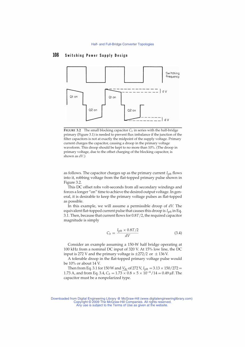
108 S w i t c h i n g P o w e r S u p p l y D e s i g n
FIGURE 3.2 The small blocking capacitor Cb in series with the half-bridgeprimary (Figure 3.1) is needed to prevent flux imbalance if the junction of thefilter capacitors is not at exactly the midpoint of the supply voltage. Primarycurrent charges the capacitor, causing a droop in the primary voltagewaveform. This droop should be kept to no more than 10%. (The droop inprimary voltage, due to the offset charging of the blocking capacitor, isshown as dV.)
as follows. The capacitor charges up as the primary current Ipft flowsinto it, robbing voltage from the flat-topped primary pulse shown inFigure 3.2.
This DC offset robs volt-seconds from all secondary windings andforces a longer “on” time to achieve the desired output voltage. In gen-eral, it is desirable to keep the primary voltage pulses as flat-toppedas possible.
In this example, we will assume a permissible droop of dV. Theequivalent flat-topped current pulse that causes this droop is Ipft in Eq.3.1. Then, because that current flows for 0.8T/2, the required capacitormagnitude is simply
Cb = Ipft × 0.8T/2dV
(3.4)
Consider an example assuming a 150-W half bridge operating at100 kHz from a nominal DC input of 320 V. At 15% low line, the DCinput is 272 V and the primary voltage is ±272/2 or ± 136 V.
A tolerable droop in the flat-topped primary voltage pulse wouldbe 10% or about 14 V.
Then from Eq. 3.1 for 150 W and Vdc of 272 V, Ipft = 3.13 × 150/272 =1.73 A, and from Eq. 3.4, Cb = 1.73 × 0.8 × 5 × 10−6/14 = 0.49 μF. Thecapacitor must be a nonpolarized type.
Downloaded from Digital Engineering Library @ McGraw-Hill (www.digitalengineeringlibrary.com)Copyright © 2009 The McGraw-Hill Companies. All rights reserved.
Any use is subject to the Terms of Use as given at the website.
Half- and Full-Bridge Converter Topologies

C h a p t e r 3 : H a l f - a n d F u l l - B r i d g e C o n v e r t e r T o p o l o g i e s 109
3.2.5 Half-Bridge LeakageInductance Problems
Leakage inductance spikes, which are so troublesome in the single-ended forward converter and push-pull topology, are easily avoidedin the half bridge: they are clamped to Vdc by the clamping diodes D5,D6 across transistors Q1, Q2.
Assuming Q1 is “on,” the load and magnetizing currents flowthrough it and through the primary leakage inductance of T1, theparalleled T1 magnetizing inductance, and the secondary loadimpedances that are reflected by their turn ratios squared into theprimary. Then it flows through Cb into the C1, C2 junction. The dotend of Np is positive with respect to its no-dot end.
When Q1 turns “off,” the magnetizing inductance forces all windingpolarities to reverse. The dot end of T1 starts to go negative by flybackaction, and if this were to continue, it would put more than Vdc acrossQ1 and could damage it. Also, Q2 could be damaged by imposing areverse voltage across it. However, the dot end of T1 is clamped bydiode D6 to the supply rail Vdc and can go no more negative than thenegative end of the supply.
Similarly, when Q2 is “on,” it stores current in the magnetizinginductance, and the dot end of Np is negative with respect to the no-dotend (which is close to Vdc/2). When Q2 turns “off,” the magnetizinginductance reverses all winding polarities by flyback action and thedot end of Np tries to go positive but is caught at Vdc by clamp diodeD5. Thus the energy stored in the leakage inductance during the “on”time is returned to the supply rail Vdc via diodes D5, D6.
3.2.6 Double-Ended Forward Convertervs. Half Bridge
Both the half-bridge and double-ended forward converter (Figure2.13) subject their respective “off” state transistors to only Vdc andnot twice that. Thus, they are both candidates for the European mar-ket where the prime power is 220 V AC. Both methods have beenused in such applications in enormous numbers, and it is instructiveto consider the relative merits and drawbacks of each approach.
The most significant difference between the two approaches is thatthe half-bridge secondary provides full-wave output as comparedwith half-wave in the forward converter. Thus, the square-wave fre-quency in the half-bridge secondary is twice that in the forward con-verter, and hence, the output LC inductor and capacitor are smallerwith the half bridge.
After Pressman The term frequency, when applied to double-ended andsingle-ended converters, is not helpful. It is easier to consider secondary pulse
Downloaded from Digital Engineering Library @ McGraw-Hill (www.digitalengineeringlibrary.com)Copyright © 2009 The McGraw-Hill Companies. All rights reserved.
Any use is subject to the Terms of Use as given at the website.
Half- and Full-Bridge Converter Topologies

110 S w i t c h i n g P o w e r S u p p l y D e s i g n
repetition rate. If the pulse rate is the same for both types (conventionally,doubling the frequency of the single-ended case), the power throughput willbe the same. It is just a matter of convention rather than a basic differencein power ratings. In the push-pull case, each positive and negative half cycleproduces an output pulse resulting in two pulses per cycle (pulse frequencydoubling). So simply producing two pulses from the single-ended topologyin the same time period results in the same output.
The real difference between the two is that the push-pull takes the flux inthe core from a negative position on the BH loop to a positive position and,conversely, while the single-ended goes from zero to positive only. Potentiallythe push-pull has twice the flux range. However, above about 50 kHz, thep-p flux swing is limited by core loss to less than 200 mT typically, a fluxswing that can be obtained easily from both the push-pull and single-endedtopologies. ∼K.B.
Peak secondary voltages are higher with the forward converterbecause the duty cycle is half that of the half bridge. This is significantonly if DC output voltages are high—greater than 200 V, as discussedin Section 2.5.1.
There are twice as many turns on the forward converter primaryas on the half bridge because the former must sustain the full supplyvoltage as compared with half that voltage in the half bridge. Havingfewer turns on the half-bridge primary may reduce its winding costand result in lower parasitic capacities.
After Pressman Although there are less turns on the half bridge, thecurrent is doubled and copper loss is proportional to I2, so the wire must betwice the diameter for the same copper loss. ∼K.B.
One final marginal factor in favor of the half bridge is that the coillosses in the primary due to the proximity effect (Section 7.5.6.1) areslightly lower than in the forward converter.
Proximity effect losses are caused by eddy currents induced in onewinding layer by currents in adjacent layers. Proximity losses increaserapidly with the number of winding layers, and the forward convertermay have more layers. The half-bridge primary has half the turns ofa double-ended forward converter primary of equal output poweroperating from the same DC supply voltage. However, this is balancedsomewhat by the larger wire size required for the half bridge. Thus,the required number of circular mils for a forward converter primaryis given by Eq. 2.42 as 985Po/Vdc and for a half bridge by Eq. 3.3 as1395Po/Vdc.
In a practical case, the lower proximity effect losses for the halfbridge may be only a marginal advantage. Proximity effect losses willbe discussed in more detail in Chapter 7.
Downloaded from Digital Engineering Library @ McGraw-Hill (www.digitalengineeringlibrary.com)Copyright © 2009 The McGraw-Hill Companies. All rights reserved.
Any use is subject to the Terms of Use as given at the website.
Half- and Full-Bridge Converter Topologies
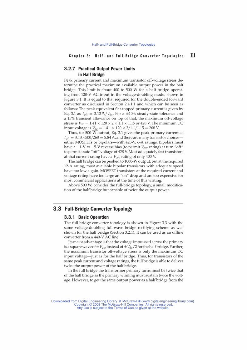
C h a p t e r 3 : H a l f - a n d F u l l - B r i d g e C o n v e r t e r T o p o l o g i e s 111
3.2.7 Practical Output Power Limitsin Half Bridge
Peak primary current and maximum transistor off-voltage stress de-termine the practical maximum available output power in the halfbridge. This limit is about 400 to 500 W for a half bridge operat-ing from 120-V AC input in the voltage-doubling mode, shown inFigure 3.1. It is equal to that required for the double-ended forwardconverter as discussed in Section 2.4.1.1 and which can be seen asfollows: The peak equivalent flat-topped primary current is given byEq. 3.1 as Ipft = 3.13Po/Vdc. For a ±10% steady-state tolerance anda 15% transient allowance on top of that, the maximum off-voltagestress is Vdc = 1.41 × 120 × 2 × 1.1 × 1.15 or 428 V. The minimum DCinput voltage is Vdc = 1.41 × 120 × 2/1.1/1.15 = 268 V.
Thus, for 500-W output, Eq. 3.1 gives the peak primary current asIpft = 3.13×500/268 = 5.84 A, and there are many transistor choices—either MOSFETs or bipolars—with 428-V, 6-A ratings. Bipolars musthave a −1-V to −5-V reverse bias (to permit Vcev rating) at turn “off”to permit a safe “off” voltage of 428 V. Most adequately fast transistorsat that current rating have a Vceo rating of only 400 V.
The half bridge can be pushed to 1000-W output, but at the required12-A rating, most available bipolar transistors with adequate speedhave too low a gain. MOSFET transistors at the required current andvoltage rating have too large an “on” drop and are too expensive formost commercial applications at the time of this writing.
Above 500 W, consider the full-bridge topology, a small modifica-tion of the half bridge but capable of twice the output power.
3.3 Full-Bridge Converter Topology3.3.1 Basic OperationThe full-bridge converter topology is shown in Figure 3.3 with thesame voltage-doubling full-wave bridge rectifying scheme as wasshown for the half bridge (Section 3.2.1). It can be used as an offlineconverter from a 440-V AC line.
Its major advantage is that the voltage impressed across the primaryis a square wave of ±Vdc, instead of ±Vdc/2 for the half bridge. Further,the maximum transistor off-voltage stress is only the maximum DCinput voltage—just as for the half bridge. Thus, for transistors of thesame peak current and voltage ratings, the full bridge is able to delivertwice the output power of the half bridge.
In the full bridge the transformer primary turns must be twice thatof the half bridge as the primary winding must sustain twice the volt-age. However, to get the same output power as a half bridge from the
Downloaded from Digital Engineering Library @ McGraw-Hill (www.digitalengineeringlibrary.com)Copyright © 2009 The McGraw-Hill Companies. All rights reserved.
Any use is subject to the Terms of Use as given at the website.
Half- and Full-Bridge Converter Topologies
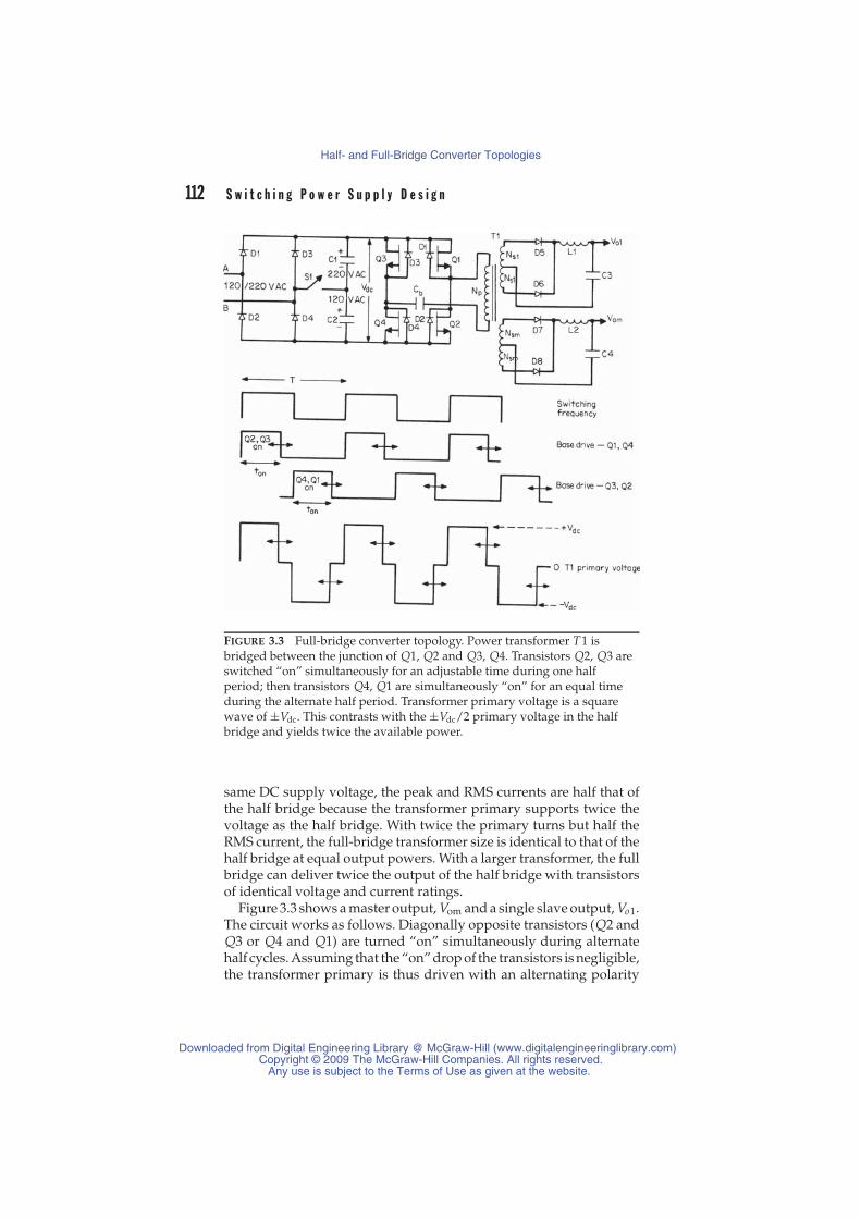
112 S w i t c h i n g P o w e r S u p p l y D e s i g n
FIGURE 3.3 Full-bridge converter topology. Power transformer T1 isbridged between the junction of Q1, Q2 and Q3, Q4. Transistors Q2, Q3 areswitched “on” simultaneously for an adjustable time during one halfperiod; then transistors Q4, Q1 are simultaneously “on” for an equal timeduring the alternate half period. Transformer primary voltage is a squarewave of ±Vdc. This contrasts with the ±Vdc/2 primary voltage in the halfbridge and yields twice the available power.
same DC supply voltage, the peak and RMS currents are half that ofthe half bridge because the transformer primary supports twice thevoltage as the half bridge. With twice the primary turns but half theRMS current, the full-bridge transformer size is identical to that of thehalf bridge at equal output powers. With a larger transformer, the fullbridge can deliver twice the output of the half bridge with transistorsof identical voltage and current ratings.
Figure 3.3 shows a master output, Vom and a single slave output, Vo1.The circuit works as follows. Diagonally opposite transistors (Q2 andQ3 or Q4 and Q1) are turned “on” simultaneously during alternatehalf cycles. Assuming that the “on” drop of the transistors is negligible,the transformer primary is thus driven with an alternating polarity
Downloaded from Digital Engineering Library @ McGraw-Hill (www.digitalengineeringlibrary.com)Copyright © 2009 The McGraw-Hill Companies. All rights reserved.
Any use is subject to the Terms of Use as given at the website.
Half- and Full-Bridge Converter Topologies
C h a p t e r 3 : H a l f - a n d F u l l - B r i d g e C o n v e r t e r T o p o l o g i e s 113
square wave of amplitude Vdc and “on” time ton determined by thefeedback loop.
The feedback loop senses a fraction of Vom, and the pulse widthmodulator controls ton so as to keep Vom constant against line and loadchanges. The slave outputs, as in all other topologies, are kept con-stant against AC line input changes, but only to within about 5 to 8%against load changes. If we assume a 1-V “on” drop in each switchingtransistor, 0.5-V forward drop in the master output Schottky rectifiers,and 1.0-V forward drops in the slave output rectifiers, we get
Vom =[
(Vdc − 2)Nsm
Np− 0.5
]2ton
T(3.5a)
Vom ≈ VdcNsm
Np
2ton
T(3.5b)
Vo1 =[
(Vdc − 2)Ns1
Np− 1
]2ton
T(3.6a)
Vo1 ≈ VdcNs1
Np
2ton
T(3.6b)
As in all pulse width modulated regulators, as Vdc goes up or downby a given percentage, the width modulator decreases or increases the“on” time by the same percentage so as to keep the product (Vdc)(ton)and, hence, the output voltages constant.
3.3.2 Full-Bridge Magnetics3.3.2.1 Maximum “On” Time, Core, and Primary Turns SelectionIn Figure 3.3, it can be seen that if two transistors that are verticallystacked above one another (Q3 and Q4, or Q1 and Q2) are turned“on” simultaneously, they would present a dead short-circuit acrossthe DC supply bus and the transistors would fail. To ensure this doesnot happen, the maximum “on” time ton will be chosen as 80% of ahalf period. This is “chosen” by selecting the turns ratios Nsm/Np ,Ns1/Np , so that in those equations for Vdc , with ton equal to 0.8T/2,the correct output voltages—Vom, Vo1—are obtained. The maximum“on” time occurs at minimum DC input voltage Vdc—as can be seenin Eqs. 3.5b and 3.6b.
The magnetic core and operating frequency are chosen from thecore-frequency selection chart in Chapter 7. With a core selected andits iron area Ae known, the number of primary turns Np is chosenfrom Faraday’s law (Eq. 1.17). In Eq. 1.17, E is the minimum primaryvoltage
(Vdc − 2
), and dB is the flux change desired in the time dt of
0.8T/2. As discussed in Section 2.2.9.4, dB will be chosen as 3200 G
Downloaded from Digital Engineering Library @ McGraw-Hill (www.digitalengineeringlibrary.com)Copyright © 2009 The McGraw-Hill Companies. All rights reserved.
Any use is subject to the Terms of Use as given at the website.
Half- and Full-Bridge Converter Topologies

114 S w i t c h i n g P o w e r S u p p l y D e s i g n
(−1600 to +1600 G) for frequencies up to 50 kHz and this will bereduced at higher frequencies because core losses increase.
3.3.2.2 Relation Between Input Voltage, Primary Current,and Output Power
Assume an efficiency of 80% from the primary input to the total outputpower. Then
Po = 0.8Pin or Pin = 1.25Po
At minimum DC input voltage Vdc, on time per half period is 0.8T/2,and duty cycle over a complete period is 0.8. Then neglecting thepower transistor on drops, input power at Vdc is
Pin = Vdc(0.8) Ipft = 1.25Po
or
Ipft = 1.56Po
Vdc(3.7)
where Ipft is the equivalent primary flat-topped current as describedin Section 2.2.10.1.
3.3.2.3 Primary Wire Size SelectionCurrent Ipft flows at a duty cycle of 0.8 so its RMS value is
Irms = Irms√
0.8.
Then, from Eq. 3.7
Irms = (1.56Po/Vdc)√
0.8
Irms = 1.40Po
Vdc(3.8)
And at a current density of 500 circular mils per RMS ampere, therequired number of circular mils is
Circular mils needed = 500 × 1.40Po
Vdc
= 700Po
Vdc(3.9)
3.3.2.4 Secondary Turns and Wire SizeThe number of turns on each secondary is calculated from Eqs. 3.5aand 3.5b, where ton is 0.8T/2 for the specified minimum DC input
Downloaded from Digital Engineering Library @ McGraw-Hill (www.digitalengineeringlibrary.com)Copyright © 2009 The McGraw-Hill Companies. All rights reserved.
Any use is subject to the Terms of Use as given at the website.
Half- and Full-Bridge Converter Topologies

C h a p t e r 3 : H a l f - a n d F u l l - B r i d g e C o n v e r t e r T o p o l o g i e s 115
Vdc, Np as calculated in Section 3.3.2.1, and all DC outputs arespecified.
Secondary RMS currents and wire sizes are chosen exactly as for thepush-pull secondaries as described in Section 2.2.10.3. The secondaryRMS currents are given by Eq. 2.13 and the required circular mils foreach half secondary is given by Eq. 2.14.
3.3.3 Output Filter CalculationsFor the half-bridge and push-pull topologies that have full-wave out-put rectifiers, the output inductor and capacitors are calculated fromEqs. 2.20 and 2.22. Equation 2.20 specifies the output inductor forminimum DC output currents equal to one-tenth the nominal values.Equation 2.22 specifies the output capacitor for the specified peak-to-peak output ripple Vr and the selected peak-to-peak inductor currentripple amplitude.
3.3.4 Transformer PrimaryBlocking Capacitor
Figure 3.3 shows a small nonpolarized blocking capacitor Cb in serieswith the transformer. It is needed to avoid the flux-imbalance problemas discussed in Section 3.2.4.
Flux imbalance in the full bridge is less likely than in the half bridge,but still is possible. With bipolars, an “on” pair in one half cycle mayhave different storage times than the pair in the alternate half cycle.With MOSFETs, the “on” state voltage drops of the pairs for alternatehalf cycles may be unequal. In either case, if the volt-second productapplied to the transformer primary in alternate half cycles is unequal,the core could walk off the center of the hysteresis loop, saturate thecore, and destroy the transistors.
Downloaded from Digital Engineering Library @ McGraw-Hill (www.digitalengineeringlibrary.com)Copyright © 2009 The McGraw-Hill Companies. All rights reserved.
Any use is subject to the Terms of Use as given at the website.
Half- and Full-Bridge Converter Topologies

Downloaded from Digital Engineering Library @ McGraw-Hill (www.digitalengineeringlibrary.com)Copyright © 2009 The McGraw-Hill Companies. All rights reserved.
Any use is subject to the Terms of Use as given at the website.
Half- and Full-Bridge Converter Topologies
C H A P T E R 4Flyback Converter
Topologies
ForewordI find that many engineers and students have great difficulty with thedesign of flyback type converters. This is unfortunate because thesetopologies are very useful, and, in fact, they are not difficult to design.
The problem is not the intrinsic difficulty of the subject matter (orthe ability of the student). The fault is related to the way the subject istraditionally taught.
Right from the start the normal term flyback transformer immediatelyprojects the wrong mindset. Not unreasonably, designers set out todesign a “flyback transformer” as if it were a real transformer. This isnot the way to go.
We are all very familiar with transformers, very simple devicesreally—we put a voltage across a primary winding and we get a volt-age on a secondary winding. The voltage ratio follows the turns ratio,irrespective of the output (or load) current. In other words, the trans-former conserves the voltage transfer ratio (one volt per turn on theprimary results in one volt per turn on the secondary. You want tenvolts? Then use ten turns, very simple). However, notice an importantproperty of transformers, the primary and secondary conduct at thesame time. If current flows into the start of the primary winding itflows out of the start of the secondary winding at the same time.
Figure 4.1 shows the basic schematic of a flyback converter. Noticethe when Q1 is “on” current flows into the primary winding of T1 butthe secondary diodes are not conducting and there is no secondary cur-rent. When Q1 turns “off” the primary current stops, all winding volt-ages reverse by flyback action, and the output diodes and secondarywindings now conduct current. So the primary and secondary wind-ings in the flyback “transformer” conduct current at different times.This apparently minor difference dramatically changes the rules.
117Downloaded from Digital Engineering Library @ McGraw-Hill (www.digitalengineeringlibrary.com)
Copyright © 2009 The McGraw-Hill Companies. All rights reserved.Any use is subject to the Terms of Use as given at the website.
Source: Switching Power Supply Design
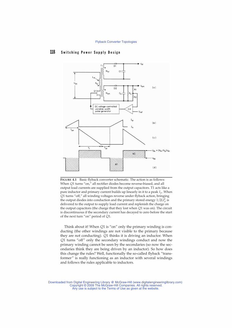
118 S w i t c h i n g P o w e r S u p p l y D e s i g n
FIGURE 4.1 Basic flyback converter schematic. The action is as follows:When Q1 turns “on,” all rectifier diodes become reverse-biased, and alloutput load currents are supplied from the output capacitors. T1 acts like apure inductor and primary current builds up linearly in it to a peak Ip . WhenQ1 turns “off,” all winding voltages reverse under flyback action, bringingthe output diodes into conduction and the primary stored energy 1/2LI2
p isdelivered to the output to supply load current and replenish the charge onthe output capacitors (the charge that they lost when Q1 was on). The circuitis discontinuous if the secondary current has decayed to zero before the startof the next turn “on” period of Q1.
Think about it! When Q1 is “on” only the primary winding is con-ducting (the other windings are not visible to the primary becausethey are not conducting). Q1 thinks it is driving an inductor. WhenQ1 turns “off” only the secondary windings conduct and now theprimary winding cannot be seen by the secondaries (so now the sec-ondaries think they are being driven by an inductor). So how doesthis change the rules? Well, functionally the so-called flyback “trans-former” is really functioning as an inductor with several windingsand follows the rules applicable to inductors.
Downloaded from Digital Engineering Library @ McGraw-Hill (www.digitalengineeringlibrary.com)Copyright © 2009 The McGraw-Hill Companies. All rights reserved.
Any use is subject to the Terms of Use as given at the website.
Flyback Converter Topologies

C h a p t e r 4 : F l y b a c k C o n v e r t e r T o p o l o g i e s 119
The rules for an inductor with more than one winding are as follows:The primary to secondary ampere-turns ratios are conserved (not thevoltage ratios, as was the case with a true transformer). For example,if the primary is, say, 100 turns and the current when Q1 turns “off” is1 amp, then we have developed 100 ampere-turns in the primary. Thismust be conserved in the secondaries. With, say, a single secondarywinding of 10 turns, the secondary current will be 10 amps (10T ×10A = 100 ampere-turns). In the same way, a single turn will develop100 amps or 1000 secondary turns will develop 0.1 amps.
So where do we stand with regard to voltage? Well, to the first order,there is no correlation between primary and secondary voltages. Thesecondary voltage is simply a function of load. Consider the 10-turn10-amp (100 ampere-turns) secondary winding example mentionedabove. If we terminate the winding with a 1-ohm load, we will get10 volts. What is more striking because the 10 amps must be con-served is that if we terminate it with 100 ohms, we will get 1000 volts!This is why the flyback topology is so useful for generating high volt-ages (don’t try to open circuit this winding because it will destroythe semiconductors). With several secondary windings conducting atthe same time, then the sum of all the secondary ampere-turns mustbe conserved.
So the lesson we learn here is that flyback “transformers” actuallyoperate as inductors and must be designed as such. (In Chapter 7, Iuse the term choke instead of inductor because the core must supportboth DC and AC components of current.) If flyback “transformers”had originally been called by their correct functional name, “flybackchokes,” then a lot of confusion could have been avoided.
We must not forget that voltage transformation is still taking placebetween primary and secondary windings even if they are not con-ducting at the same time. Taking the above example of 10 turns termi-nated in 100 ohms, the 1000 volts thus developed on this secondarywinding will reflect back to the primary as 10,000 volts; this addedto the supply of 100 volts will stress Q1 in its “off” state with 10,100volts (where did I put that 11,000 volt transistor?). Hardly practical,but the theory holds.
So when designing flyback transformers keep the following keypoints in mind:
1. Remember you are not designing a transformer, you are design-ing a choke with additional windings.
2. The primary turns are selected to satisfy the AC voltage stress(volt-seconds) and the core AC saturation properties:
Np = VTB Ae
Downloaded from Digital Engineering Library @ McGraw-Hill (www.digitalengineeringlibrary.com)Copyright © 2009 The McGraw-Hill Companies. All rights reserved.
Any use is subject to the Terms of Use as given at the website.
Flyback Converter Topologies

120 S w i t c h i n g P o w e r S u p p l y D e s i g n
Where Np is minimum primary turnsV is the maximum primary DC voltage (volts)T is the maximum “on” period for Q1 (microseconds)B is the AC p-p flux swing (tesla) typically 200 mT for
ferriteAe is the effective center pole area of the core (mm2)
3. The secondary turns are optional. If you choose the same voltsper turn on the secondary as was used for the primary, then theflyback voltage on Q1 will be twice the supply voltage.
4. When using a gapped ferrite core, the minimum core gap mustbe such that the core will not saturate for the sum of DC and ACmagnetization current. More often the gap is chosen to satisfythe power transfer requirements. This normally results in a gapexceeding the minimum requirements. Remember the energystored in the primary is
E(joules) = 1/2LI2
Remember this is the maximum energy that can be transferredto the secondary, and then only in the discontinuous (completeenergy transfer) mode. In the continuous mode, only part of thisenergy is transferred.
Note Although reducing the inductance L may appear to reduce thestored energy, the current I increases in the same ratio as the induc-tance decreases. Since the I parameter is squared, the stored energyactually increases as L decreases.
5. It is not recommended that you try to design for a defined in-ductance. It is better to let inductance be a dependant variableas changing the core gap or core material (permeability) willchange the inductance.
Below in Chapter 4, Pressman follows the conventional “flybacktransformer” approach, providing a very complete analysis. Thereader may find it helpful to first read Chapter 7 in this book andPart 2, Chapters 1 and 2 in my book, shown as Reference 1 at the endof this chapter.
4.1 IntroductionAll the topologies previously discussed (with the exception of theboost regulator Section 1.4 and the polarity inverter Section 1.5)deliver power to their loads during the period when the power tran-sistor is turned “on.”
Downloaded from Digital Engineering Library @ McGraw-Hill (www.digitalengineeringlibrary.com)Copyright © 2009 The McGraw-Hill Companies. All rights reserved.
Any use is subject to the Terms of Use as given at the website.
Flyback Converter Topologies
C h a p t e r 4 : F l y b a c k C o n v e r t e r T o p o l o g i e s 121
However, the flyback topologies described in this chapter operatein a fundamentally different way. During the power transistor “on”time, they store energy in the power transformer. During this period,the load current is supplied from an output filter capacity only. Whenthe power transistor turns “off,” the energy stored in the power trans-former is transferred to the load and to the output filter capacitoras it replaces the charge it lost when it alone was delivering loadcurrent.
The flyback has advantages and limitations, discussed in more de-tail later. A major advantage is that the output filter inductors nor-mally required for all forward topologies are not required for flybacktopologies because the transformer serves both functions. This is par-ticularly valuable in low-cost multiple output power supplies yieldinga significant saving in cost and space.
4.2 Basic Flyback Converter SchematicThe basic flyback converter topology together with typical currentand voltage waveforms is shown in Figure 4.1. It is very widely usedfor low-cost applications in the power range from about 150 W downto less than 5 W. Its great initial attraction is immediately clear—it hasno secondary output inductor, and the consequent saving in cost andvolume is a significant advantage.
In Figure 4.1, flyback operation can be easily recognized fromthe position of the dots on the transformer primary and secondary(these dots show the starts of the windings). When Q1 is “on,” thedot ends of all windings are negative with respect to their no-dotends. Output rectifier diodes D1 and D2 are reverse-biased and allthe output load currents are supplied from storage filter capacitorsC1 and C2. These will be chosen as described below to deliver theload currents with the maximum specified ripple or droop in outputvoltages.
4.3 Operating ModesThere are two distinctly different operating modes for flyback con-verters: the continuous mode and the discontinuous mode. The wave-forms, performance, and transfer functions are quite different for thetwo modes, and typical waveforms are shown in Figure 4.2. The valueof primary inductance and the load current determine the mode ofoperation.
Downloaded from Digital Engineering Library @ McGraw-Hill (www.digitalengineeringlibrary.com)Copyright © 2009 The McGraw-Hill Companies. All rights reserved.
Any use is subject to the Terms of Use as given at the website.
Flyback Converter Topologies
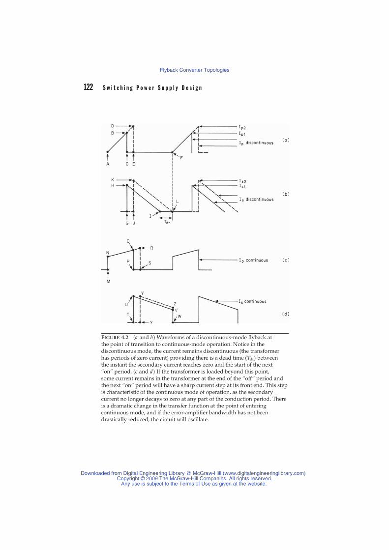
122 S w i t c h i n g P o w e r S u p p l y D e s i g n
FIGURE 4.2 (a and b) Waveforms of a discontinuous-mode flyback atthe point of transition to continuous-mode operation. Notice in thediscontinuous mode, the current remains discontinuous (the transformerhas periods of zero current) providing there is a dead time (Tdt) betweenthe instant the secondary current reaches zero and the start of the next“on” period. (c and d) If the transformer is loaded beyond this point,some current remains in the transformer at the end of the “off” period andthe next “on” period will have a sharp current step at its front end. This stepis characteristic of the continuous mode of operation, as the secondarycurrent no longer decays to zero at any part of the conduction period. Thereis a dramatic change in the transfer function at the point of enteringcontinuous mode, and if the error-amplifier bandwidth has not beendrastically reduced, the circuit will oscillate.
Downloaded from Digital Engineering Library @ McGraw-Hill (www.digitalengineeringlibrary.com)Copyright © 2009 The McGraw-Hill Companies. All rights reserved.
Any use is subject to the Terms of Use as given at the website.
Flyback Converter Topologies
C h a p t e r 4 : F l y b a c k C o n v e r t e r T o p o l o g i e s 123
4.4 Discontinuous-Mode OperationFigure 4.1 shows a master output and one slave output. As in allother topologies shown previously, a negative-feedback loop will beclosed around the master output Vom. A fraction of Vom will be com-pared to a reference, and the error signal will control the “on” timeof Q1 (the pulse width), so as to regulate the sampled output volt-age equal to the reference voltage against line and load changes.Hence, the master output is fully regulated. However, the slaveswill also be well regulated against line changes and somewhat lesswell against load changes because the secondary winding voltagestend to track the master voltage. As a result, the slave line and loadregulation is better than for the previously discussed forward-typetopologies.
During the Q1 “on” time, there is a fixed voltage across Np andcurrent in it ramps up linearly (Figure 4.1b) at a rate of dI/dt = (Vdc−1)/L p , where L p is the primary magnetizing inductance. At the end of the“on” time, the primary current has ramped up to Ip = (Vdc−1)Ton/L p .This current represents a stored energy of
E = L p( Ip)2
2(4.1)
where E is in joulesL p is in henriesIp is in amperes
Now when Q1 turns “off,” the current in the magnetizing induc-tance forces a reversal of polarities on all windings. (This is called fly-back action.) Assume, for the moment, that there are no slave windingsand only the master secondary Nm. Since the current in an inductorcannot change instantaneously, at the instant of turn “off,” the primarycurrent transfers to the secondary at an amplitude Is = Ip(Np/Nm).
After a number of cycles, the secondary DC voltage has built up to amagnitude (calculated below) of Vom. Now with Q1 “off,” the dot endof Nm is positive with respect to its no-dot end and current flows outof it, but ramps down linearly (Figure 4.1c) at a rate dIs/dt = Vom/Vs ,where Ls is the secondary inductance. The discontinuous mode actionis defined as follows.
If the secondary current has ramped down to zero before the startof the next Q1 “on” time, all the energy stored in the primary whenQ1 was “on” has been delivered to the load and the circuit is said tobe operating in the discontinuous mode.
Since an amount of energy E in joules delivered in a time T inseconds represents input power in watts, we can calculate the input
Downloaded from Digital Engineering Library @ McGraw-Hill (www.digitalengineeringlibrary.com)Copyright © 2009 The McGraw-Hill Companies. All rights reserved.
Any use is subject to the Terms of Use as given at the website.
Flyback Converter Topologies

124 S w i t c h i n g P o w e r S u p p l y D e s i g n
power as follows: At the end of one period, power P drawn fromVdc is
P =1/2 L p( Ip)2
TW (4.2a)
But Ip = (Vdc − 1)Ton/L p . Then
P = [(Vdc − 1)Ton]2
2TLp≈ (VdcTon)2
2TLpW (4.2b)
As can be seen from Eq. 4.2b, the feedback loop maintains constantoutput voltage by keeping the product VdcTon constant.
4.4.1 Relationship Between Output Voltage,Input Voltage, “On” Time, andOutput Load
Let us assume an efficiency of 80%, then
Input power = 1.25 (output power)
= 1.25(Vo )2
Ro=
1/2(L p I 2p)
T
But Ip = VdcTon/L p since maximum “on” time Ton occurs at mini-mum supply voltage Vdc, as can be seen from Eq. 4.2b.
Then 1.25 (Vo )2/Ro = 1/2 L pVdc2T2
on/L2pT or
Vo = VdcTon
√Ro
2.5TLp(4.3)
Thus the feedback loop will regulate the output by decreasing Tonas Vdc or Ro goes up, increasing Ton as Vdc Ro goes down.
4.4.2 Discontinuous-Mode toContinuous-Mode Transition
In Figures 4.2a and 4.2b the solid lines represent primary and sec-ondary currents in the discontinuous mode. Primary current is a tri-angle starting from zero and rising to a level Ip1 (point B) at the endof the power transistor “on” time.
At the instant of Q1 turn “off,” the current Ip1 established in theprimary winding is transferred to the secondary so as to maintain theampere-turns ratio. This current is dumped into the secondary capac-itors and load during the “off” period. The secondary current rampsdownward at a rate dIs/dt = (Vo + 1)/Ls , where Ls is the secondary
Downloaded from Digital Engineering Library @ McGraw-Hill (www.digitalengineeringlibrary.com)Copyright © 2009 The McGraw-Hill Companies. All rights reserved.
Any use is subject to the Terms of Use as given at the website.
Flyback Converter Topologies

C h a p t e r 4 : F l y b a c k C o n v e r t e r T o p o l o g i e s 125
inductance, which is (Ns/Np)2 times the primary magnetizing induc-tance. This current reaches zero at time I, leaving a dead time Tdtbefore the start of the next turn “on” period at point F . All the currentand hence energy stored in the primary during the previous “on” pe-riod has now been completely delivered to the load before the nextturn “on.” The average DC output current will be the average of thetriangle GHI multiplied by its duty cycle of Toff/T .
Now, to remain in the discontinuous mode, there must be a deadtime Tdt (Figure 4.2b) between the time the secondary current hasdropped to zero and the start of the next power transistor “on” time.As more power is demanded (by decreasing Ro ), Ton must increaseto keep output voltage constant (see Eq. 4.3). As Ton increases (atconstant Vdc), primary current slope remains constant and the peakcurrent rises from B to D as shown in Figure 4.2a . Secondary peakcurrent (= Ip Np/Ns) increases from H to K in Figure 4.2b and startslater in time (from G to J).
Since the output voltage is kept constant by the feedback loop, thesecondary slope Vo/Ls remains constant and the point at which thesecondary current falls to zero moves closer to the start of the next turn“on.” This reduces Tdt until a point L is reached where the secondarycurrent has just fallen to zero at the instant of the next turn “on.”This load current marks the end of the discontinuous mode. Noticethat if the supply voltage falls, the “on” time Ton must increase as Vdcdecreases to maintain constant output voltage and this will have thesame effect.
Notice that as long as the circuit is in the discontinuous mode sothat a dead time always remains, increasing the “on” time increasesthe area of the primary and secondary current triangle GHI up tothe limit of the area JKL. Further, since the DC output current isthe average of the secondary current triangle multiplied by its dutycycle, then during the very next “off” period following an increasein “on” time, more secondary current is immediately available to theload.
When the dead time has been lost, however, any further increasein load current demand will increase the “on” time and decrease the“off” time as the back end of the secondary current can no longermove to the right. The secondary current will start later than point J(Figure 4.2b) and from a higher point than K. Then at the start of thenext “on” period (position F in Figure 4.2a or L in Figure 4.2b), thereis still some current or energy left in the transformer.
Now the front end of the primary current will have a small step. Thefeedback loop tries to deliver the increased DC load current demandby keeping the “on” time later than point J. Now at each successive“off” time, the current remaining at the end of the “off” time andhence the current step at the start of the next “on” time increase.
Downloaded from Digital Engineering Library @ McGraw-Hill (www.digitalengineeringlibrary.com)Copyright © 2009 The McGraw-Hill Companies. All rights reserved.
Any use is subject to the Terms of Use as given at the website.
Flyback Converter Topologies

126 S w i t c h i n g P o w e r S u p p l y D e s i g n
Finally after many switching cycles, the front-end step of primarycurrent and the back-end current at the end of the “off” time in Figure4.2d are sufficiently high so that the area XYZW is somewhat largerthan that sufficient to supply the output load current. Now the feed-back loop starts to decrease the “on” time so that the primary trapezoidlasts from M to P and the secondary current trapezoid lasts from T toW (Figures 4.2a and 4.2b).
At this point, the volt-seconds across the transformer primary whenthe power transistor is “on” is equal to the “off” volt-seconds acrossit when the transistor is “off.” For this condition, the transformer coreis always reset to its original point on the hysteresis loop at the end ofa full cycle. It is also the condition where the average or DC voltageacross the primary is zero. This is an essential requirement, since theDC resistance in the primary is near zero and it is not possible tosupport a long-term DC voltage across zero resistance.
Once the continuous mode has been established, increased loadcurrent is supplied initially by an increase in “on” time (from MPto MS in Figure 4.2c). For fixed-frequency operation this results in adecrease in “off” time from TW to XW (Figure 4.2d) as the back endof the secondary current pulse cannot move further to the right intime because the dead time has vanished. Although the peak of thesecondary current has increased somewhat (from point U to Y), thearea lost in the decreased “off” time (T to X) is greater than the areagained in the slope change from UV to YZ in Figure 4.2d .
Thus, in the continuous mode, a sudden increase in DC outputcurrent initially causes a decrease in width and a smaller increasein height of the secondary current trapezoid. After many switchingcycles, the average trapezoid height builds up and the width relaxesback to the point where the “on” volt-seconds again equals the “off”volt-seconds across the primary.
In addition, since the DC output voltage is proportional to the areaof the secondary current trapezoid, the feedback loop, in attemptingto keep the output voltage constant against an increased current de-mand, first drastically decreases the output voltage and then, aftermany switching cycles, corrects it by building up the amplitude of thesecondary current trapezoid. This is the physical-circuits significanceof the so-called right-half-plane-zero, which forces the drastic reduc-tion in error-amplifier bandwidth to stabilize the feedback loop. Theright-half-plane-zero will be discussed further in the chapter on loopstabilization.
After Pressman In a fixed-frequency system, the immediate effect of in-creasing the “on” period (to increase primary and hence output current)will be to decrease the “off” period (the period for transfer of current tothe output). Since the inductance of the transformer prevents rapid changes
Downloaded from Digital Engineering Library @ McGraw-Hill (www.digitalengineeringlibrary.com)Copyright © 2009 The McGraw-Hill Companies. All rights reserved.
Any use is subject to the Terms of Use as given at the website.
Flyback Converter Topologies

C h a p t e r 4 : F l y b a c k C o n v e r t e r T o p o l o g i e s 127
in current, the immediate effect of trying to increase current is to cause ashort-term decrease in output current. (This is a transitory 180◦ phase shiftbetween cause and effect). This short transitory phase shift is the cause ofthe right-half-plane-zero in the transfer function. It is a non-compensatabledynamic effect and forces the designer to provide a very low-frequency roll offin the control loop to maintain stability. Hence transient performance willnot be good. The flyback converter in the continuous mode has a boost-likeconverter characteristic and any converter or combination of converters thathave a boost-type characteristic will have the right-half-plane-zero problem.∼K.B.
4.4.3 Continuous-Mode Flyback—Basic Operation
The flyback topology is widely used for high output voltages at rela-tively low power (≤5000 V at <15 W). It can also be used at powers ofup to 150 W if DC supply voltages are high enough (≥160 V) so thatprimary currents are not excessive. The feature which makes it valu-able for high output voltages is that it requires no output inductor. Inforward converters, discussed above, output inductors become a trou-blesome problem at high output voltages because of the large voltagesthey have to sustain. Not requiring a high voltage free-wheeling diodeis also a plus for the flyback in high voltage supplies.
After Pressman A further advantage for high voltage applications isthat relatively large voltages can be obtained with relatively fewer trans-former turns. ∼K.B.
The flyback topology is attractive for multiple output supplies be-cause the output voltages track one another for line and load changes,far better than they do in the forward-type converters described ear-lier. The absence of output inductors results in better tracking. As aresult, flybacks are a frequent choice for supplies with many outputvoltages (up to 10 isolated outputs are not uncommon). The powercan be in the range of 50 to 150 W.
Although they can be used from DC input voltages as low as 5 V,it is more usual to find them used for the usual rectified 160 VDCobtained from a 115-V AC power line input. By careful design of theturns ratios, they can also be used in universal line input applicationsranging from the rectified output of 160 volts DC from 110 AC inputsup to the 320 V DC obtained from a 220-V AC power line, without theneed for the voltage doubling–full-wave rectifying scheme (switch S1)shown in Figure 3.1.
The latter scheme, although very widely used, has the objectionablefeature that to do the switching from 115 to 220 V AC, both ends of
Downloaded from Digital Engineering Library @ McGraw-Hill (www.digitalengineeringlibrary.com)Copyright © 2009 The McGraw-Hill Companies. All rights reserved.
Any use is subject to the Terms of Use as given at the website.
Flyback Converter Topologies

128 S w i t c h i n g P o w e r S u p p l y D e s i g n
the switch in Figure 3.1 have to be accessible on the outside of thesupply, which is a safety hazard. Or the supply must be opened tochange the switch position. Both these alternatives have drawbacks.An alternative scheme not requiring switching will be discussed inSection 4.3.5.
Both modes have an identical circuit diagram, shown in Figure 4.1,and it is only the transformer’s magnetizing inductance and outputload current that determines the operating mode. It has been shownthat with a given magnetizing inductance, a circuit that has been de-signed for the discontinuous mode will move into the continuousmode when the output load current is increased beyond a uniqueboundary. The mechanism for this and its consequence are discussedin more detail below.
The discontinuous mode (as shown in Figure 4.2a ) does not havea front-end step in the primary current. At turn “off” (as shown inFigure 4.2b), the secondary current will be a decaying triangle thathas ramped down to zero before the next turn “on.” All the energystored in the primary during the “on” period has been completelydelivered to the secondary and thus to the load before the next turn“on.”
In the continuous mode, however (as seen in Figure 4.2c), the pri-mary current does have a front-end step and the characteristic of arising current ramp following the step. During the “off” period ofQ1 (Figure 4.2d), the secondary current has the shape of a decay-ing triangle sitting on a step with current still remaining in the sec-ondary at the instant of the next turn “on” action. Clearly there isstill some energy left in the transformer at the instant of the next turn“on.”
The two modes have significantly different operating proper-ties and usages. The discontinuous mode, which does not have aright-half-plane-zero in the transfer function, responds more rapidlyto transient load changes with a lower transient output voltagespike.
A penalty is paid for this performance, in that the secondary peakcurrent in the discontinuous mode can be between two and three timesgreater than that in the continuous mode. This is shown in Figures4.2b and 4.2d . Secondary DC load current is the average of the currentwaveshapes in those figures. Also, assuming closely equal “off” times,it is obvious that the triangle in the discontinuous mode must have amuch larger peak than the trapezoid of the continuous mode for thetwo waveshapes to have equal average values.
With larger peak secondary currents, the discontinuous mode hasa larger transient output voltage spike at the instant of turn “off”(Section 4.3.4.1) and requires a larger LC spike filter to remove it.
Downloaded from Digital Engineering Library @ McGraw-Hill (www.digitalengineeringlibrary.com)Copyright © 2009 The McGraw-Hill Companies. All rights reserved.
Any use is subject to the Terms of Use as given at the website.
Flyback Converter Topologies

C h a p t e r 4 : F l y b a c k C o n v e r t e r T o p o l o g i e s 129
Also, the larger secondary peak current at the start of turn “off” in thediscontinuous mode causes a greater RFI problem. Even for moderateoutput powers, the very large initial spike of secondary current atthe instant of turn “off” causes a much more severe noise spike onthe output ground bus, because of the large di/dt into the output businductance.
After Pressman A major advantage of the discontinuous mode is thatthe secondary rectifier diodes turn “off” under low current stress conditions.Also they are fully “off” before the next “on” edge of Q1. Hence the problemof diode reverse recovery is eliminated. This is a major advantage in highvoltage applications as diode reverse recovery current spikes are difficult toeliminate and are a rich source of RFI. ∼K.B.
Due to the poor form factor, secondary RMS currents in the dis-continuous mode can be much larger than those in the continuousmode. Hence, the discontinuous mode requires larger secondary wiresize and output filter capacitors with larger ripple current ratings.The rectifier diodes will also run hotter in the discontinuous modebecause of the larger secondary RMS currents. Further, the primarypeak currents in the discontinuous mode are larger than those in thecontinuous mode. For the same output power, the triangle of Figure4.2a must have a larger peak than the trapezoid of Figure 4.2c. Theconsequence is that the discontinuous mode with its larger peak pri-mary current requires a power transistor of higher current rating andpossibly higher cost. Also, the higher primary current at the turn “off”edge of Q1 results in a potential for greater RFI problems.
Despite all the disadvantages of the discontinuous mode, it is muchmore widely used than the continuous mode. This is so for two rea-sons. First, as mentioned above, the discontinuous mode, with an in-herently smaller transformer magnetizing inductance, responds morequickly and with a lower transient output voltage spike to rapidchanges in output load current or input voltage. Second, because of aunique characteristic of the continuous mode (its transfer function hasa right-half-plane-zero, to be discussed in a later chapter on feedbackloop stabilization), the error amplifier bandwidth must be drasticallyreduced to stabilize the feedback loop.
After Pressman Modern power devices, such as the Power Integration’sTop Switch range of products, have the “noisy” FET drain part of the chipisolated from the heat sink tab. This, together with integrated drive andcontrol circuits, which further reduce radiating area, very much reduces theRFI problems normally associated with the discontinuous flyback topology.∼K.B.
Downloaded from Digital Engineering Library @ McGraw-Hill (www.digitalengineeringlibrary.com)Copyright © 2009 The McGraw-Hill Companies. All rights reserved.
Any use is subject to the Terms of Use as given at the website.
Flyback Converter Topologies

130 S w i t c h i n g P o w e r S u p p l y D e s i g n
4.5 Design Relations and SequentialDesign Steps4.5.1 Step 1: Establish the
Primary/Secondary Turns RatioFor the most expedient design, there are a number of decisions thatshould be made in the following logical sequence.
First select a core size to meet the power requirements.Next choose the primary/master secondary turns ratio Np/Nsm to
determine the maximum “off”-voltage stress Vms on the power tran-sistor in the absence of a leakage inductance spike as follows:
Neglecting the leakage spike, the maximum transistor voltage stressat maximum DC input Vdc and for a 1-V rectifier drop is
Vms = Vdc + Np
Nsm(Vo + 1) (4.4)
where Vms is chosen sufficiently low so that a leakage inductance spikeof 0.3Vdc on top of that still leaves a safety margin of about 30% belowthe maximum pertinent transistor rating (Vceo, Vcer, or Vcev).
4.5.2 Step 2: Ensure the Core Does NotSaturate and the Mode RemainsDiscontinuous
To ensure that the core does not drift up or down its hysteresis loop,the “on” volt-second product (A1 in Figure 4.1d) must equal the resetvolt-second product (A2 in Figure 4.1d). Assume that the “on” dropof Q1 and the forward drop of the rectifier D2 are both 1 V:
(Vdc − 1)Ton = (Vo + 1)Np
NsmTr (4.5)
where Tr shown in Figure 4.1c is the reset time required for the sec-ondary current to return to zero.
To ensure the circuit operates in the discontinuous mode, a deadtime (Tdt in Figure 4.1c) is established so that the maximum “on” timeTon, which occurs when Vdc is a minimum, plus the reset time Tr isonly 80% of a full period. This leaves 0.2T margin against unexpecteddecreases in Ro , which according to Eq. 4.3 would force the feedbackloop to increase Ton in order to keep Vo constant.
As for the boost regulator, which is also a flyback type (Sections 1.4.2and 1.4.3), it was pointed out that if the error amplifier has been de-signed to keep the loop stable only in the discontinuous mode, it maybreak into oscillation if the circuit momentarily enters the continuousmode.
Downloaded from Digital Engineering Library @ McGraw-Hill (www.digitalengineeringlibrary.com)Copyright © 2009 The McGraw-Hill Companies. All rights reserved.
Any use is subject to the Terms of Use as given at the website.
Flyback Converter Topologies

C h a p t e r 4 : F l y b a c k C o n v e r t e r T o p o l o g i e s 131
Increasing DC load current or decreasing Vdc causes the error ampli-fier to increase Ton in order to keep Vo constant (Eq. 4.3). This increasedTon eats into the dead time Tdt, and eventually the secondary currentdoes not fall to zero by the start of the next Q1 “on” time. This is thestart of the continuous mode, and if the error amplifier has not beendesigned with a drastically lower bandwidth than required for dis-continuous mode, the circuit will oscillate. To ensure that the circuitremains discontinuous, the maximum “on” time that will generate thedesired maximum output power is established:
Ton + Tr + Tdt = T
or
Ton + Tr = 0.8T (4.6)
Now in Eqs. 4.5 and 4.6, there are two unknowns, as Np/Nsm has beencalculated from Eq. 4.4 for specified Vdc and Vms. Then from the lasttwo relations
Ton = (Vo + 1)(Np/Nsm)(0.8T)(Vdc − 1) + (Vo + 1)(Np/Nsm)
(4.7)
4.5.3 Step 3: Adjust the Primary InductanceVersus Minimum Output Resistanceand DC Input Voltage
From Eq. 4.3, the primary inductance is
L p = Ro
2.5T
(VdcTon
Vo
)2
= (VdcTon)2
2.5T Po(4.8)
4.5.4 Step 4: Check Transistor Peak Currentand Maximum Voltage Stress
If the transistor is a bipolar type, it must have an acceptably high gainat the peak current operating current Ip. This is
Ip = VdcTon
L p(4.9)
where Vdc is specified and Ton is calculated from Eq. 4.7 and L p iscalculated from Eq. 4.8.
If Q1 is a MOSFET, it should have a peak current rating about 5 to 10times the value calculated from Eq. 4.9 so that its “on”-state resistanceis low enough to yield an acceptably low voltage drop and power loss.
Downloaded from Digital Engineering Library @ McGraw-Hill (www.digitalengineeringlibrary.com)Copyright © 2009 The McGraw-Hill Companies. All rights reserved.
Any use is subject to the Terms of Use as given at the website.
Flyback Converter Topologies

132 S w i t c h i n g P o w e r S u p p l y D e s i g n
4.5.5 Step 5: Check Primary RMS Currentand Establish Wire Size
The primary current is a triangle of peak amplitude Ip (Eq. 4.9) at amaximum duration Ton out of every period T . Its RMS value (Section2.2.10.6) is
Irms(primary) = Ip√3
√Ton
T(4.10)
where Ip and Ton are as given by Eqs. 4.9 and 4.7.At 500 circular mils per RMS ampere, the required number of cir-
cular mils is
Circular mils required (primary) = 500 Irms(primary)
= 500Ip√
3
√Ton
T(4.11)
4.5.6 Step 6: Check Secondary RMS Currentand Select Wire Size
The secondary current is a triangle of peak amplitude Is = Ip(Np/Ns)and duration Tr . Primary/secondary turns ratio Np/Ns is given byEq. 4.4 and Tr = (T − Ton). Secondary RMS current is then
Irms(secondary) = Ip(Np/Ns)√3
√Tr
T(4.12)
At 500 circular mils per RMS ampere, the required number of cir-cular mils is
Secondary circular mils required = 500Irms(secondary) (4.13)
4.6 Design Example for a Discontinuous-ModeFlyback ConverterWe will now look at a worked design example for a flyback converterwith the following specifications:
Vo 5.0 V
Po(max) 50 W
Io(max) 10 A
Io(min) 1.0 A
Vdc(max) 60 V
Vdc(min) 38 V
Switching frequency 50 kHz
Downloaded from Digital Engineering Library @ McGraw-Hill (www.digitalengineeringlibrary.com)Copyright © 2009 The McGraw-Hill Companies. All rights reserved.
Any use is subject to the Terms of Use as given at the website.
Flyback Converter Topologies

C h a p t e r 4 : F l y b a c k C o n v e r t e r T o p o l o g i e s 133
First, select the voltage rating of the transistor as this mainly de-termines the transformer turns ratio. Choose a device with a 200-Vrating. In Eq. 4.4 choose the maximum stress Vms on the transistor inthe “off” state (excluding the leakage inductance spike) as 120 V. Theneven with a 25% or 30-V leakage spike, this leaves a 50-V margin tothe maximum voltage rating. Then from Eq. 4.4
120 = 60 + Np
Nsm(Vo + 1) or
Np
Nsm= 10
Now choose maximum “on” time from Eq. 4.7:
Tom = (Vo + 1)(Np/Nsm)(0.8T)(Vdc − 1) + (Vo + 1)Np/Nsm
= 6 × 10 × 0.8 × 20(38 − 1) + 6 × 10
= 9.9 μs
From Eq. 4.8
L p = (VdcTon)2
2.5T Po
= (38 × 9.9 × 10−6)2
2.5 × 20 × 10−6 × 50
= 56.6 μH
From Eq. 4.9
Ip = VdcTon
L p
= 38 × 9.9 × 10−6
56.6 × 10−6
= 6.6 A
From Eq. 4.10, primary RMS current is
Irms(primary) = Ip√3
√Ton
T
= 6.6√3
×√
9.920
= 2.7 A
Downloaded from Digital Engineering Library @ McGraw-Hill (www.digitalengineeringlibrary.com)Copyright © 2009 The McGraw-Hill Companies. All rights reserved.
Any use is subject to the Terms of Use as given at the website.
Flyback Converter Topologies

134 S w i t c h i n g P o w e r S u p p l y D e s i g n
From Eq. 4.11, primary circular mils requirement is
I(primary circular mils) = 500 × 2.7 = 1350 circular mils
This calls for a No. 19 wire of 1290 circular mils, which is close enough.From Eq. 4.12, secondary RMS current is
Irms(secondary) = Ip(Np/Ns)√3
√Tr
T
But reset time Tr is
(0.8T − Ton) = (16 − 9.9) = 6.1 μs
Then
Irms(secondary) = 6.6 × 10√3
√6.120
= 21 A
We see that from Eq. 4.12, the required number of circular mils is500 × 21 = 10,500. This calls for No. 10 wire, which is impracticallylarge in diameter. A foil winding or a number of smaller diameterwires in parallel with an equal total circular-mil area would be used.
After Pressman Contrary to popular belief, the wire size and leakage in-ductance in a flyback transformer are important design parameters. Multiplestrands of wire in parallel are required, with the maximum wire size selectedto minimize skin and proximity effects. Even though the secondary energycomes from the energy stored in the transformer core, leakage inductancemust still be minimized to ensure good energy transfer from the primarywinding to the secondary windings to reduce voltage spikes on Q1 at the“off” transition. This will reduce the amount of snubbing required on Q1and reduce RFI. (See Chapter 7.) ∼K.B.
The output capacitor is chosen on the basis of specified peak-to-peak output voltage ripple as follows:
At maximum output current, the filter capacitor Co carries the 10-Aoutput current for all but the 6.1 μs reset period, or 13.9 μs. The voltageon this capacitor droops by V = I (T − toff)/Co . Then for a voltagedroop of 0.05 V
Co = 10 × 13.9 × 10−6
0.05= 2800 μF
Downloaded from Digital Engineering Library @ McGraw-Hill (www.digitalengineeringlibrary.com)Copyright © 2009 The McGraw-Hill Companies. All rights reserved.
Any use is subject to the Terms of Use as given at the website.
Flyback Converter Topologies

C h a p t e r 4 : F l y b a c k C o n v e r t e r T o p o l o g i e s 135
From Section 1.4.7, the average ESR of a 2800-μF aluminum elec-trolytic capacitor is
Resr = 65 × 10−6/Co = 0.023 �
At the instant of transistor turn “off,” a peak secondary current of66 amps flows through the above capacitor ESR, causing a thin spikeof 66 × 0.023 = 1.5 V. This large-amplitude thin spike at transistor turn“off” is a universal problem with flybacks having a large Np/Ns ratio.It is usually solved by using a larger filter capacitor than calculated asabove (since Resr is inversely proportional to Co ) and/or integratingaway the thin spike with a small LC circuit.
After Pressman Since the spike contains a large amount of high fre-quency components, combining several capacitors in parallel will reduce thespike amplitude significantly. Small ceramic and film caps are often used.∼K.B.
Selecting a transformer core for a flyback topology circuit is sig-nificantly different than selecting for a forward converter. Rememberin the flyback that when current flows in the primary, the secondarycurrent is zero, and there is no current flow in the secondary to buckout the primary ampere turns as there is in the forward converters.Thus in the flyback, all the primary ampere turns tend to saturate thecore.
In contrast, in non-flyback topologies, secondary load current flowswhen primary current flows and is in the direction (by Lenz’s law) tocancel the ampere turns of the primary. It is only the primary magne-tizing current that drives the core over its hysteresis loop and moves ittoward saturation. That magnetizing current is kept a small fraction ofthe primary load current by providing a large magnetizing inductanceand hence core saturation is not a basic a problem with non-flybacktopologies.
Hence, flyback transformer cores must have some means of carryinglarge primary currents without saturating. This is done by choosinglow permeability materials such as MPP (molybdenum permalloypowder) cores that have an inherent air gap or by using gapped ferritecores (Section 2.3.9.3 and Chapter 7). This is discussed further in thefollowing section.
4.6.1 Flyback MagneticsReferring to Figure 4.1a , it is seen from the winding dots that whenthe transistor is “on” and current flows in the primary, no secondarycurrents flow. This is totally different from forward-type converters,
Downloaded from Digital Engineering Library @ McGraw-Hill (www.digitalengineeringlibrary.com)Copyright © 2009 The McGraw-Hill Companies. All rights reserved.
Any use is subject to the Terms of Use as given at the website.
Flyback Converter Topologies

136 S w i t c h i n g P o w e r S u p p l y D e s i g n
in which current flows in the secondary when it flows in the primary.Thus in a forward-type converter, primary current flows into a dotend and secondary current flows out of a dot end.
Primary and secondary load ampere-turns then cancel each otherout and do not move the core across its hysteresis loop. In the forward-type converters, it is only the magnetizing current that drives thecore across the hysteresis loop and may potentially saturate it. Butthis magnetizing current is a small fraction (rarely >10%) of the totalprimary current.
In a flyback converter, however, the entire triangle of primary cur-rent shown in Figure 4.1b drives the core across the hysteresis loop asit is not canceled out by any secondary ampere turns. Thus, even atvery low output power, an ungapped ferrite core would almost im-mediately saturate and destroy the transistor if nothing were done toprevent it.
To prevent core saturation in the flyback transformer, the core isgapped. The gapped core can be either of two types. It can be a solidferrite core with a known air-gap length obtained by grinding downthe center leg in EE or cup-type cores. The known gap length can alsobe obtained by inserting plastic shims between the two halves of anEE, cup, or UU core.
A more usual gapped core for flyback converters is the MPP ormolypermalloy powder core. Such cores are made of a baked andhardened mix of magnetic powdered particles. These powdered par-ticles are mixed in a slurry with a plastic resin binder and cast in theshape of a toroid. Each magnetic particle in the toroid is thus encapsu-lated within a resin envelope that behaves as a “distributed air gap”and acts to keep the core from saturating. The basic magnetic materialthat is ground up into a powder is Square Permalloy 80, an alloy of79% nickel, 17% iron, and 4% molybdenum, made by Magnetics Inc.and Arnold Magnetics, among others.
The permeability of the resulting toroid is determined by control-ling the concentration of magnetic particles in the slurry. Permeabili-ties are controlled to within ±5% over large temperature ranges andare available in discrete steps ranging from 14 to 550. Toroids withlow permeability behave like gapped cores with large air gaps. Theyrequire a relatively large number of turns to yield a desired inductancebut tolerate many ampere-turns before they saturate. Higher perme-ability cores require relatively fewer turns but saturate at a lowernumber of ampere-turns.
Such MPP cores are used not only for flyback transformers inwhich all the primary current is DC bias current. They are also usedfor forward converter output inductors where, as has been seen, aunique inductance is required at the large DC output current bias(Section 1.3.6).
Downloaded from Digital Engineering Library @ McGraw-Hill (www.digitalengineeringlibrary.com)Copyright © 2009 The McGraw-Hill Companies. All rights reserved.
Any use is subject to the Terms of Use as given at the website.
Flyback Converter Topologies
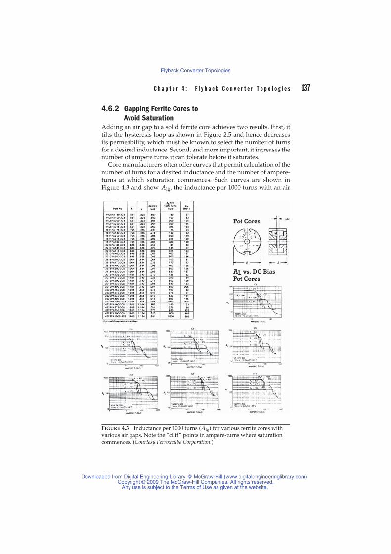
C h a p t e r 4 : F l y b a c k C o n v e r t e r T o p o l o g i e s 137
4.6.2 Gapping Ferrite Cores toAvoid Saturation
Adding an air gap to a solid ferrite core achieves two results. First, ittilts the hysteresis loop as shown in Figure 2.5 and hence decreasesits permeability, which must be known to select the number of turnsfor a desired inductance. Second, and more important, it increases thenumber of ampere turns it can tolerate before it saturates.
Core manufacturers often offer curves that permit calculation of thenumber of turns for a desired inductance and the number of ampere-turns at which saturation commences. Such curves are shown inFigure 4.3 and show Alg, the inductance per 1000 turns with an air
FIGURE 4.3 Inductance per 1000 turns (Alg) for various ferrite cores withvarious air gaps. Note the “cliff” points in ampere-turns where saturationcommences. (Courtesy Ferroxcube Corporation.)
Downloaded from Digital Engineering Library @ McGraw-Hill (www.digitalengineeringlibrary.com)Copyright © 2009 The McGraw-Hill Companies. All rights reserved.
Any use is subject to the Terms of Use as given at the website.
Flyback Converter Topologies

138 S w i t c h i n g P o w e r S u p p l y D e s i g n
gap and the number of ampere-turns (NIsat) where saturation starts toset in. Since inductance is proportional to the square of the number ofturns, the number of turns Nl for any inductance L is calculated from
Nl = 1000
√L
Alg(4.14)
Figure 4.3 shows Alg curves for a number of different air gaps and the“cliff” point at which saturation starts. It can be seen that the largerthe air gap, the lower the value of Alg and the larger the number ofampere-turns at which saturation starts. If such curves were availablefor all cores at various air gaps, Eq. 4.14 would give the number of turnsfor any selected air gap from the value of Alg read from the curve. Thecliff point on the curve would tell whether, at those turns and for thespecified primary current, the core had fallen over the saturation cliff.
Such curves, though, are not available for all cores and all air gaps.This is no problem, because Alg can be calculated with reasonableaccuracy from Eq. 2.39 using Al with no gap, which is always givenin the manufacturers’ catalogs. The cliff point at which saturationstarts can be calculated from Eq. 2.37 for any air gap. The cliff pointcorresponds to the flux density in iron Bi , where the core materialitself starts bending over into saturation.
From Figure 2.3, it is seen that this is not a very sharp breakingpoint, but occurs around 2500 G for this ferrite material (Ferroxcube3C8). Thus the cliff in ampere-turns is found by substituting 2500 Gin Eq. 2.37. As noted in connection with Eq. 2.37, in the usual case, theair-gap length la is much larger than li/u as u is so large. Then the ironflux density as given by Eq. 2.37 is determined mainly by the air-gaplength la .
4.6.3 Using Powdered Permalloy (MPP)Cores to Avoid Saturation
These toroidal cores are widely used and made by Magnetics Inc. (datain catalog MPP303S) and by Arnold Co. (data in catalog PC104G).
After Pressman The term transformer in the phrase flyback trans-former is a misnomer and is very misleading. For true transformer actionto take place both primary and secondaries must conduct current at the sametime. We are all aware that a true transformer conserves the primary to sec-ondary voltage ratio (irrespective of current). In the flyback case the so-calledtransformer conserves the primary to secondary ampere-turns ratio (irrespec-tive of voltage). This means it is really a “choke”—an inductor with a DCcomponent of current and additional windings. I find it much easier and lessconfusing to design my flyback “transformers” from this perspective. Thereader may also find it helpful to use this approach because the inductance
Downloaded from Digital Engineering Library @ McGraw-Hill (www.digitalengineeringlibrary.com)Copyright © 2009 The McGraw-Hill Companies. All rights reserved.
Any use is subject to the Terms of Use as given at the website.
Flyback Converter Topologies

C h a p t e r 4 : F l y b a c k C o n v e r t e r T o p o l o g i e s 139
becomes the dependant variable and can be easily adjusted to get the desiredresults. Chapter 7 deals with the design in this way.
You will see from the following that although he does not mention it, Press-man is leading you in the direction of choke design. ∼K.B.
The problem in designing a core of desired inductance at a specifiedmaximum DC current bias is to select a core geometry and materialpermeability, such that the core does not saturate at the maximumampere-turns to which it is subjected. There are a limited numberof core geometries, each available in permeabilities ranging from 14to 550. Selection procedures are described in the catalogs mentionedabove, but the following has been found more direct and useful.
In the Magnetics Inc. catalog, one full page (Figure 4.4) is devotedto each size toroid, and for each size, its Al value (inductance in milli-henries per 1000 turns) is given for each discrete permeability. Figure4.5, also from the Magnetics Inc. catalog, gives the falloff in permeabil-ity (or Al value) for increasing magnetizing force in oersteds for corematerials of the various available permeabilities. (Recall the oersted–ampere-turns relation in Eq. 2.6.)
A core geometry and permeability can be selected so that at themaximum DC current and the selected number of turns, the Al andhence inductance has fallen off by any desired percentage given inFigure 4.5. Then at zero DC current, the inductance will be greater bythat percentage. Such inductors or chokes are referred to as “swing-ing chokes” and in many applications are desirable. For example, ifan inductor is permitted to swing a great deal, in an output filter, itcan tolerate a very low minimum DC current before it goes discon-tinuous (Section 1.3.6). But this greatly complicates the feedback-loopstability design and, most often, the inductor in an output filter ortransformer in a flyback will not be permitted to “swing” or vary verymuch between its zero and maximum current value.
Referring to Figure 4.4, it is seen that a core of this specific size isavailable in permeabilities ranging from 14 to 550. Cores with perme-ability above 125 have large values of Al and hence require fewer turnsfor a specified inductance at zero DC current bias. But in Figure 4.5it is seen that the higher-permeability cores saturate at increasinglylower ampere-turns of bias. Hence in power supply usage, where DCcurrent biases are rarely under 1 A, cores of permeability greater than125 are rarely used, and an inductance swing or change of 10% fromzero to the maximum specified current is most often acceptable.
In Figure 4.5, it is seen that for a permeability dropoff or swing of10%, core materials of permeabilities 14, 26, 60, and 125 can sustainmaximum magnetizing forces of only 170, 95, 39, and 19 Oe, respec-tively. These maximum magnetizing forces in oersteds can be trans-lated into maximum ampere-turns by Eq. 2.6 (H = 0.4π(NI )/ lm), in
Downloaded from Digital Engineering Library @ McGraw-Hill (www.digitalengineeringlibrary.com)Copyright © 2009 The McGraw-Hill Companies. All rights reserved.
Any use is subject to the Terms of Use as given at the website.
Flyback Converter Topologies
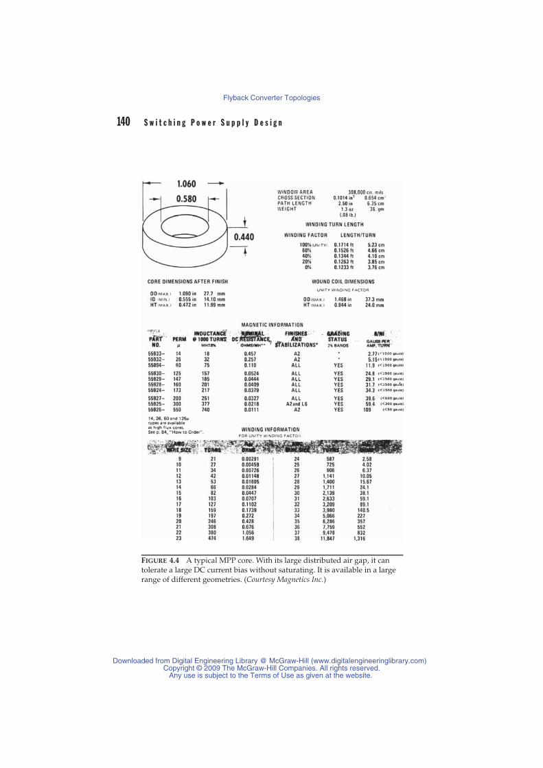
140 S w i t c h i n g P o w e r S u p p l y D e s i g n
FIGURE 4.4 A typical MPP core. With its large distributed air gap, it cantolerate a large DC current bias without saturating. It is available in a largerange of different geometries. (Courtesy Magnetics Inc.)
Downloaded from Digital Engineering Library @ McGraw-Hill (www.digitalengineeringlibrary.com)Copyright © 2009 The McGraw-Hill Companies. All rights reserved.
Any use is subject to the Terms of Use as given at the website.
Flyback Converter Topologies
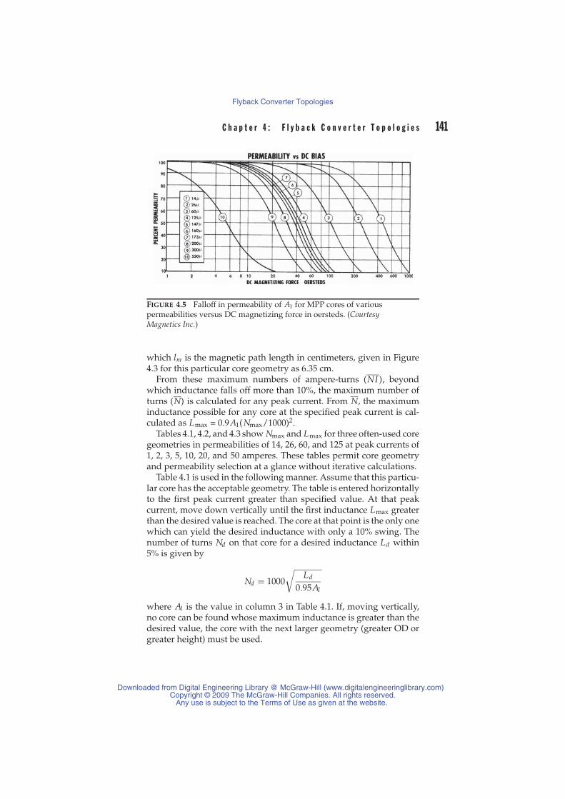
C h a p t e r 4 : F l y b a c k C o n v e r t e r T o p o l o g i e s 141
FIGURE 4.5 Falloff in permeability of A1 for MPP cores of variouspermeabilities versus DC magnetizing force in oersteds. (CourtesyMagnetics Inc.)
which lm is the magnetic path length in centimeters, given in Figure4.3 for this particular core geometry as 6.35 cm.
From these maximum numbers of ampere-turns (NI ), beyondwhich inductance falls off more than 10%, the maximum number ofturns (N) is calculated for any peak current. From N, the maximuminductance possible for any core at the specified peak current is cal-culated as Lmax = 0.9A1(Nmax/1000)2.
Tables 4.1, 4.2, and 4.3 show Nmax and Lmax for three often-used coregeometries in permeabilities of 14, 26, 60, and 125 at peak currents of1, 2, 3, 5, 10, 20, and 50 amperes. These tables permit core geometryand permeability selection at a glance without iterative calculations.
Table 4.1 is used in the following manner. Assume that this particu-lar core has the acceptable geometry. The table is entered horizontallyto the first peak current greater than specified value. At that peakcurrent, move down vertically until the first inductance Lmax greaterthan the desired value is reached. The core at that point is the only onewhich can yield the desired inductance with only a 10% swing. Thenumber of turns Nd on that core for a desired inductance Ld within5% is given by
Nd = 1000
√Ld
0.95Al
where Al is the value in column 3 in Table 4.1. If, moving vertically,no core can be found whose maximum inductance is greater than thedesired value, the core with the next larger geometry (greater OD orgreater height) must be used.
Downloaded from Digital Engineering Library @ McGraw-Hill (www.digitalengineeringlibrary.com)Copyright © 2009 The McGraw-Hill Companies. All rights reserved.
Any use is subject to the Terms of Use as given at the website.
Flyback Converter Topologies

142 S w i t c h i n g P o w e r S u p p l y D e s i g n
NI
Max
imu
mM
axim
um
per
mis
sib
leM
agn
etic
sA
l,m
HH
for
10%
amp
ere-
turn
sIn
c.co
reP
erm
e-p
er10
00fa
llof
fin
corr
esp
ond
ing
Max
imu
mp
erm
issi
ble
turn
san
din
du
ctan
ceat
thos
etu
rns
nu
mb
erab
ilit
ytu
rns
ind
uct
ance
toH
for
a10
%in
du
ctan
cefa
llof
fat
ind
icat
edp
eak
curr
ents
Nm
ax/
Lm
ax
Cor
eμ
Al
HN
I1A
2A3A
5A10
A20
A50
AI p
5593
012
515
719
9696
4832
1910
52
Nm
ax1,
382
339
145
5615
3.5
0.6
Lm
ax
5589
460
7539
197
197
9966
3920
104
Nm
ax2,
620
662
294
103
277
1L
max
5593
226
3295
480
480
240
160
9648
2410
Nm
ax6,
635
1,65
973
726
566
173
Lm
ax
5593
314
1817
085
985
943
028
617
286
4317
Nm
ax11
,954
2,99
51,
325
479
120
305
Lm
ax
Not
e:M
agne
tics
Inc.
MPP
core
s.A
llco
res
have
oute
rd
iam
eter
(OD
)=1.
060
in,i
nner
dia
met
er(I
D)=
0.58
in,h
eigh
t=0.
44in
,lm
=6.
35cm
.A
llin
duc
tanc
esin
mic
rohe
nrie
s.
TA
BL
E4.
1M
axim
umnu
mbe
rof
turn
syi
eld
ing
max
imum
ind
ucta
nce
for
vari
ous
peak
curr
ents
I pat
max
imum
ind
ucta
nce
fallo
ffof
10%
from
zero
curr
ent
Downloaded from Digital Engineering Library @ McGraw-Hill (www.digitalengineeringlibrary.com)Copyright © 2009 The McGraw-Hill Companies. All rights reserved.
Any use is subject to the Terms of Use as given at the website.
Flyback Converter Topologies

C h a p t e r 4 : F l y b a c k C o n v e r t e r T o p o l o g i e s 143
NI
Max
imu
mM
axim
um
per
mis
sib
leM
agn
etic
sA
l,m
HH
for
10%
amp
ere-
turn
sIn
c.co
reP
erm
e-p
er10
00fa
llof
fin
corr
esp
ond
ing
Max
imu
mp
erm
issi
ble
turn
san
din
du
ctan
ceat
thos
etu
rns
nu
mb
erab
ilit
ytu
rns
ind
uct
ance
toH
for
a10
%in
du
ctan
cefa
llof
fat
ind
icat
edp
eak
curr
ents
Nm
ax/
Lm
ax
Cor
eμ
Al
HN
I1A
2A3A
5A10
A20
A50
AI p
5520
612
568
1977
7739
2615
84
2N
max
363
9341
144
10.
24L
max
5584
860
3239
158
158
7953
3216
83
Nm
ax71
918
081
297
20.
26L
max
5520
826
1495
385
385
193
128
7739
198
Nm
ax1,
868
469
206
7519
4.5
0.8
Lm
ax
5520
914
7.8
170
689
689
345
230
138
6934
14N
max
3,33
383
637
113
433
81.
4L
max
Not
e:M
agne
tics
Inc.
MPP
core
s:O
D=
0.8
in,I
D=
0.5
in,h
eigh
t=0.
25in
,lm
=5.
09cm
.All
ind
ucta
nces
inm
icro
henr
ies.
TA
BL
E4.
2M
axim
umnu
mbe
rof
turn
san
dm
axim
umin
duc
tanc
efo
rva
riou
spe
akcu
rren
tsI p
ata
max
imum
ind
ucta
nce
fallo
ffof
10%
from
zero
curr
ent
Downloaded from Digital Engineering Library @ McGraw-Hill (www.digitalengineeringlibrary.com)Copyright © 2009 The McGraw-Hill Companies. All rights reserved.
Any use is subject to the Terms of Use as given at the website.
Flyback Converter Topologies

144 S w i t c h i n g P o w e r S u p p l y D e s i g n
Cor
eμ
Al
HN
I1A
2A3A
5A10
A20
A50
AI p
5543
812
528
119
162
162
8154
3216
83
Nm
ax6,
637
1,65
973
725
965
162
Lm
ax
5543
960
135
3933
333
316
711
167
3317
7N
max
13,4
733,
389
1,49
754
513
235
6L
max
5544
026
5995
812
812
406
271
162
8141
16N
max
35,0
118,
753
3,90
01,
394
348
8914
Lm
ax
5544
114
3217
014
541,
454
727
485
291
145
7329
Nm
ax60
,744
15,2
226,
774
2,43
960
515
324
Lm
ax
Not
e:M
agne
tics
Inc.
MPP
core
s:O
D=
1.84
in,I
D=
0.95
in,h
eigh
t=0.
71in
,lm
=10
.74
in.A
llin
duc
tanc
esin
mic
rohe
nrie
s.
TA
BL
E4.
3M
axim
umnu
mbe
rof
turn
san
dm
axim
umin
duc
tanc
efo
rva
riou
spe
akcu
rren
tsI p
ata
max
imum
ind
ucta
nce
fallo
ffof
10%
from
zero
curr
ent
Downloaded from Digital Engineering Library @ McGraw-Hill (www.digitalengineeringlibrary.com)Copyright © 2009 The McGraw-Hill Companies. All rights reserved.
Any use is subject to the Terms of Use as given at the website.
Flyback Converter Topologies

C h a p t e r 4 : F l y b a c k C o n v e r t e r T o p o l o g i e s 145
The core ID must be large enough to accommodate the number ofturns of wire selected at the rate of 500 circular miles per RMS ampere,or the next larger size core must be used.
Tables 4.2 and 4.3 show similar data for smaller (OD = 0.80 in) andlarger (OD = 1.84 in) families of cores. Similar charts can be generatedfor all the other available core sizes, but Tables 4.1 to 4.3 bracket about90% of the possible designs for flyback transformers under 500 W oroutput inductors of up to 50 A.
A commonly used scheme for correcting the number of turns on acore when an initial selection has resulted in too large an inductancefalloff should be noted. If, for an initially selected number of turns anda specified maximum current, the inductance or permeability fallofffrom Figure 4.5 is down by P%, the number of turns is increasedby P%.
This moves the operating point further out by P%, as the magne-tizing force in oersteds is proportional to the number of turns. Thecore slides further down its saturation curve, and it might be thoughtthat the inductance would fall off even more. But since inductance isproportional to the square of the number of turns, and magnetizingforce is proportional only to the number of turns, the zero current in-ductance has been increased by 2P% and magnetizing force has goneup only by P%. The inductance is then correct at the specified maxi-mum current. If the consequent swing is too large, a larger core mustbe used.
4.6.4 Flyback DisadvantagesDespite its many advantages, the flyback has the following drawbacks.
4.6.4.1 Large Output Voltage SpikesAt the end of the “on” time, the peak primary current is given byEq. 4.9. Immediately after the end of the “on” time, that primary peakcurrent, multiplied by the turns ratio Np/Ns , is driven into the sec-ondary where it decays linearly as shown in Figure 4.1c. In most cases,output voltages are low relative to input voltage, resulting in a largeNp/Ns ratio and a consequent large secondary current.
At the start of turn “off,” the impedance looking into Co is muchlower than Ro (Figure 4.1) and almost all the large secondary currentflows into Co and its equivalent series resistor Resr. This produces alarge, thin output voltage spike, Ip(Np/Ns)Resr. The spike is generallyless than 0.5 μs in width, as it is differentiated with a time constant ofResrCo .
Frequently a power supply specification calls for output voltageripple only as an RMS or peak-to-peak fundamental value. Such alarge, thin spike has a very low RMS value and, if a sufficiently large
Downloaded from Digital Engineering Library @ McGraw-Hill (www.digitalengineeringlibrary.com)Copyright © 2009 The McGraw-Hill Companies. All rights reserved.
Any use is subject to the Terms of Use as given at the website.
Flyback Converter Topologies

146 S w i t c h i n g P o w e r S u p p l y D e s i g n
output filter capacitor is chosen, the supply can easily meet its RMSripple specification but can have disastrously high, thin output spikes.It is common to see a 50-mV fundamental peak-to-peak output ripplewith a 1-V thin spike sitting on top of it.
Thus, a small LC filter is almost always added after the main storagecapacitor in flybacks. The L and C can be quite small as they have tofilter out a spike generally less than 0.5 μs in width. The inductor isusually considerably smaller than the inductor in forward-type con-verters, but it still has to be stocked, and board space must be providedfor it. Output voltage sensing for the error amplifier is taken beforethis LC filter.
4.6.4.2 Large Output Filter Capacitor andHigh Ripple Current Requirement
A filter capacitor for a flyback must be much larger than for a forward-type converter. In a forward converter, when the power transistorturns “off” (Figure 2.10), load current is supplied from the energystored in both the filter inductor and capacitor. But in the flyback,that capacitor is necessarily larger because it is the stored energyin it alone that supplies current to the load during the transistor“on” time. Output ripple is determined mostly by the ESR of thefilter capacitor (see Section 1.3.7). An initial selection of the filtercapacitor is made on the basis of output ripple specification fromEq. 1.10.
Frequently, however, it is not the output ripple voltage requirementthat determines the final choice of the filter capacitor. Ultimately it maybe the ripple current rating of the capacitor selected initially on thebasis of the output ripple voltage specification.
In a forward-type converter (as in a buck regulator), the capacitorripple current is greatly limited by the output inductor in series withit (Section 1.3.6). In a flyback, however, the full DC load current flowsfrom common through the capacitor during the transistor “on” time.During the transistor “off” time, a charge of equal ampere-secondproduct must flow into the capacitor to replenish the charge it lostduring the “on” time. Assuming, as in Figure 4.1, a sum of “on” timeplus reset time of 80% of full period, the RMS ripple current in thecapacitor is closely
Irms = Idc
√ton
T= Idc
√0.8 = 0.89Idc (4.15)
If the capacitor initially selected on the basis of output ripple voltagespecifications did not also have the ripple current rating of Eq. 4.15, alarger capacitor or more units in parallel must be chosen.
Downloaded from Digital Engineering Library @ McGraw-Hill (www.digitalengineeringlibrary.com)Copyright © 2009 The McGraw-Hill Companies. All rights reserved.
Any use is subject to the Terms of Use as given at the website.
Flyback Converter Topologies

C h a p t e r 4 : F l y b a c k C o n v e r t e r T o p o l o g i e s 147
4.7 Universal Input Flybacks for 120-V ACThrough 220-V AC OperationHere we consider universal or wide input range flyback topologiesthat do not have the auto ranging, voltage doubling methods previ-ously described.
In Section 3.2.1, we considered a commonly used scheme that per-mitted operation from either a 120-V AC or 220-V AC line with min-imal changes. As seen in Figure 3.1 at 120 V AC, switch S1 is thrownto the lower position, making the circuit into a voltage doubler thatyields a rectified voltage of 336 V. With 220-V AC, S1 is thrown to theupper position and the circuit becomes a full-wave rectifier with C1and C2 in series, yielding about 308 V. The converter is thus designedto always work from a rectified nominal input of 308 to 336 V DC byproper choice of the transformer turns ratio.
In some applications, it is preferable to eliminate the requirementof changing S1 from one position to the other in changing from 120- to220-V AC operation. To change switch position without opening thepower supply case, the switch must be accessible externally, and this isa safety hazard. The alternative is to change the switch internally, butthis requires opening the power supply case to make the change, andthis is a nuisance. Further, there is always the possibility that the switchis mistakenly thrown to the voltage doubling position when operatedfrom 200 V AC. This, of course, would cause significant damage—thepower transistor, rectifiers, and filter capacitors would be destroyed.
An alternative is the universal line voltage unit that does not requireswitching and can tolerate the full range of line inputs from 115 to 220V AC. The rectified 115 V input will be 160 V DC and the 220 V ACwill be 310 V DC.
A flyback converter, designed with a small primary/secondaryturns ratio, can ensure that the “off”-voltage stress at high AC inputdoes not overstress the power transistor.
The maximum “on” time Ton at the minimum value of the 220-VAC input is calculated from the corresponding minimum rectified DCinput as in Eq. 4.7 and the rest of the magnetics design can proceed asshown in the text following Eq. 4.7. The minimum “on” time occursat the maximum value of the 220-V AC input. Since the feedback loopkeeps the product of VdcTon constant (Eq. 4.3), minimum “on” timeis Ton = Ton(Vdc/Vdc) where Vdc and Vdc correspond to the minimumand maximum values of the 220-V AC line.
The maximum “on” time with 115-V AC input is still given by Eq. 4.7and will be greater than with 220 V, as the term Vdc − 1 is smaller. Butthe primary inductance L p given by Eq. 4.8, which is proportionalto the product VdcTon, is still the same as that product is kept con-stant by the feedback loop. So long as the transistor can operate with
Downloaded from Digital Engineering Library @ McGraw-Hill (www.digitalengineeringlibrary.com)Copyright © 2009 The McGraw-Hill Companies. All rights reserved.
Any use is subject to the Terms of Use as given at the website.
Flyback Converter Topologies

148 S w i t c h i n g P o w e r S u p p l y D e s i g n
the minimum “on” time calculated for the maximum DC correspond-ing to high AC input, there is no problem. With bipolar transistorsoperating at a high frequency, transistor storage time could preventoperation at too low an “on” time. An example will clarify this.
Eq. 4.4 gives the maximum “off” stress in terms of the maximum DCinput voltage, the output voltage, and the Np/Ns turns ratio. Assumein that equation that Vms is 500 V; many bipolar transistors can safelysustain that voltage with a negative base bias at turn “off” (Vcev rating).At 220 V AC, the nominal Vdc is 310 V. Assume that the maximum athigh line with a worst-case transient is 375 V. Then for a 5-V output,Eq. 4.4 gives a turns ratio of 21.
Now assume that minimum DC supply voltage is 80% of nominal.Assume a switching frequency of 50 kHz (period T of 20 μs). Maxi-mum “on” time is calculated from Eq. 4.7 at the minimum DC inputcorresponding to minimum AC input of 0.8 × 115 or 92 V AC. For thecorresponding DC input of 1.41 × 92 or about 128 V, maximum “on”time calculated from Eq. 4.7 is 7.96 μs.
Minimum “on” time occurs at maximum input voltage. Assuming a20% high line, the maximum DC input is 1.2×220×1.41 = 372 V. Sincethe feedback loop keeps the product of VdcTon constant (Eq. 4.3), “on”time at the 20% high line of 264 V AC is (128/372)(7.96) or 2.74 μs. Thecircuit can thus cope with either a 20% low AC line input of 92 V ACfrom a nominal 115 V AC, or a 20% high AC input of 264 V AC fromthe nominal 220-V AC line by readjusting its “on” time from 7.96 to2.74 μs.
If this were attempted at higher switching frequencies, the mini-mum “on” time at a 220-V AC line would become so low as to prohibitthe use of bipolar transistors, which could have 0.5- to 1.0-μs storagetime. The upper-limit switching frequency at which the above schemecan be used with bipolar transistors is about 100 kHz.
It is instructive to complete the above design. Assume an outputpower of 150 W at 5-V output. Then Ro = 0.167 � and the primaryinductance from Eq. 4.8 is
Lp =(
0.1672.5 × 20 × 10−6
)(128 × 7.96 × 10−6
5
)2
= 139 μH
and the peak primary current from Eq. 4.9 is
Ip = 128 × 7.96 × 10−6
139 × 10−6 = 7.33 A
There are many reasonably priced bipolar transistors with a Vcev ratingabove 500 V having adequate gain at 7.33 A.
Downloaded from Digital Engineering Library @ McGraw-Hill (www.digitalengineeringlibrary.com)Copyright © 2009 The McGraw-Hill Companies. All rights reserved.
Any use is subject to the Terms of Use as given at the website.
Flyback Converter Topologies
C h a p t e r 4 : F l y b a c k C o n v e r t e r T o p o l o g i e s 149
Table 4.1 shows that the 55932 MPP core can tolerate a maximum of480 ampere-turns, beyond which its inductance will fall off by morethan 10% (at 5 A, column 9 shows that the maximum turns is 96 fora maximum inductance of 265 μH). For maximum ampere-turns, theinductance is 32,000 × 0.9(66/1000)2 = 125μ H. If (as discussed inSection 4.2.3.2) 10% more turns are added, the inductance at 7.33 Awill increase by 10% to 138 μH, but at zero current, the inductance will“swing” up to 20% above that.
If the 20% inductance swing is undesirable, the lower permeabilitycore 55933 of Table 4.1 can be used. Table 4.1 shows that the maximumampere-turns stress is 859. For 7.33 A, the maximum number of turnsis 859/7.33 or 117. The maximum inductance for a swing of only 10%is (0.117)2× 18000 × 0.9 or 222 μH. For the desired 139 μh, the requiredturns are 1000
√0.139/18 × 0.95 = 90.
Thus a design not requiring voltage doubling/full-wave rectifierswitching when operation is changed from 115 to 220 V AC is possible.But this subjects the power transistor to a leakage inductance spikeat turn “off” of about 500 V. The lower reliability of this scheme mustbe weighed against the use of a double-ended forward converter orhalf bridge—both of which subject the “off” transistor to only themaximum DC input (375 V in the preceding example) with no leakagespike. Of course, for 115/220-V AC operation, the rectifier switchingof Figure 3.1 must be accepted.
After Pressman Modern FETs (for example, the Power Integrations “TopSwitch” devices) very much simplify the design of universal input flybacktype supplies, which are now an accepted and standard topology for lowerpower applications. Very good application notes are available for these devices.∼K.B.
4.8 Design Relations—Continuous-ModeFlybacks4.8.1 The Relation Between Output Voltage
and “On” TimeLook once again at Figure 4.1. When the transistor Q1 is “on,” thevoltage across the primary is close to Vdc–1 with the dot end nega-tive with respect to the no-dot end, and the core is driven—say, upthe hysteresis loop. When the transistor turns “off,” the magnetiz-ing current reverses the polarity of all voltages in order to remainconstant. The primary and secondary are driven positive, but the sec-ondary is caught and clamped to Vom+ 1 by D2—assuming a 1-Vforward drop.
Downloaded from Digital Engineering Library @ McGraw-Hill (www.digitalengineeringlibrary.com)Copyright © 2009 The McGraw-Hill Companies. All rights reserved.
Any use is subject to the Terms of Use as given at the website.
Flyback Converter Topologies

150 S w i t c h i n g P o w e r S u p p l y D e s i g n
This reflects across to the primary as a voltage (Np/Ns)(Vom + 1),with the dot end now positive with respect to the no-dot end. Allthe current that was flowing in the primary (IPO in Figure 4.2c) nowtransfers to the secondary as ITU in Figure 4.2d . The initial magnitudeof the secondary current ITU is equal to the final primary current atthe end of the “on” time (IPO) times the turns ratio Np/Ns . Since thedot end of the secondary is now positive with respect to the no-dotend, the secondary current ramps downward with the slope UV inFigure 4.2d.
Since the primary is assumed to have zero DC resistance, it cannotsustain a DC voltage averaged over many cycles. Thus in the steadystate, the volt-second product across it when the transistor is “on”must equal that across it when the transistor is “off”—i.e., the voltageacross the primary averaged over a full cycle must equal zero. This isequivalent to saying the core’s downward excursion on the BH loopduring the “off” time is exactly equal to the upward excursion duringthe “on” time. Then
(Vdc − 1)ton = (Vom + 1)Np
Nstoff
or
Vom =[(
Vdc − 1) Ns
Np
ton
toff
]− 1 (4.16)
and since there is no dead time in continuous mode, ton + toff = T , and
Vom =[
(Vdc − 1)(Ns/Np)(ton/T)1 − ton/T
]− 1 (4.17a)
=[
(Vdc − 1)(Ns/Np)(T/ton) − 1
]− 1 (4.17b)
The feedback loop regulates against DC input voltage changes bydecreasing ton as Vdc increases, or increasing ton as Vdc decreases.
4.8.2 Input, Output Current–Power RelationsIn Figure 4.6, the output power is equal to the output voltage times theaverage of the secondary current pulses. For Icsr equal to the currentat the center of the ramp in the secondary current pulse
Po = Vo Icsrtoff
T= Vo Icsr(1 − ton/T)
(4.18)
Downloaded from Digital Engineering Library @ McGraw-Hill (www.digitalengineeringlibrary.com)Copyright © 2009 The McGraw-Hill Companies. All rights reserved.
Any use is subject to the Terms of Use as given at the website.
Flyback Converter Topologies
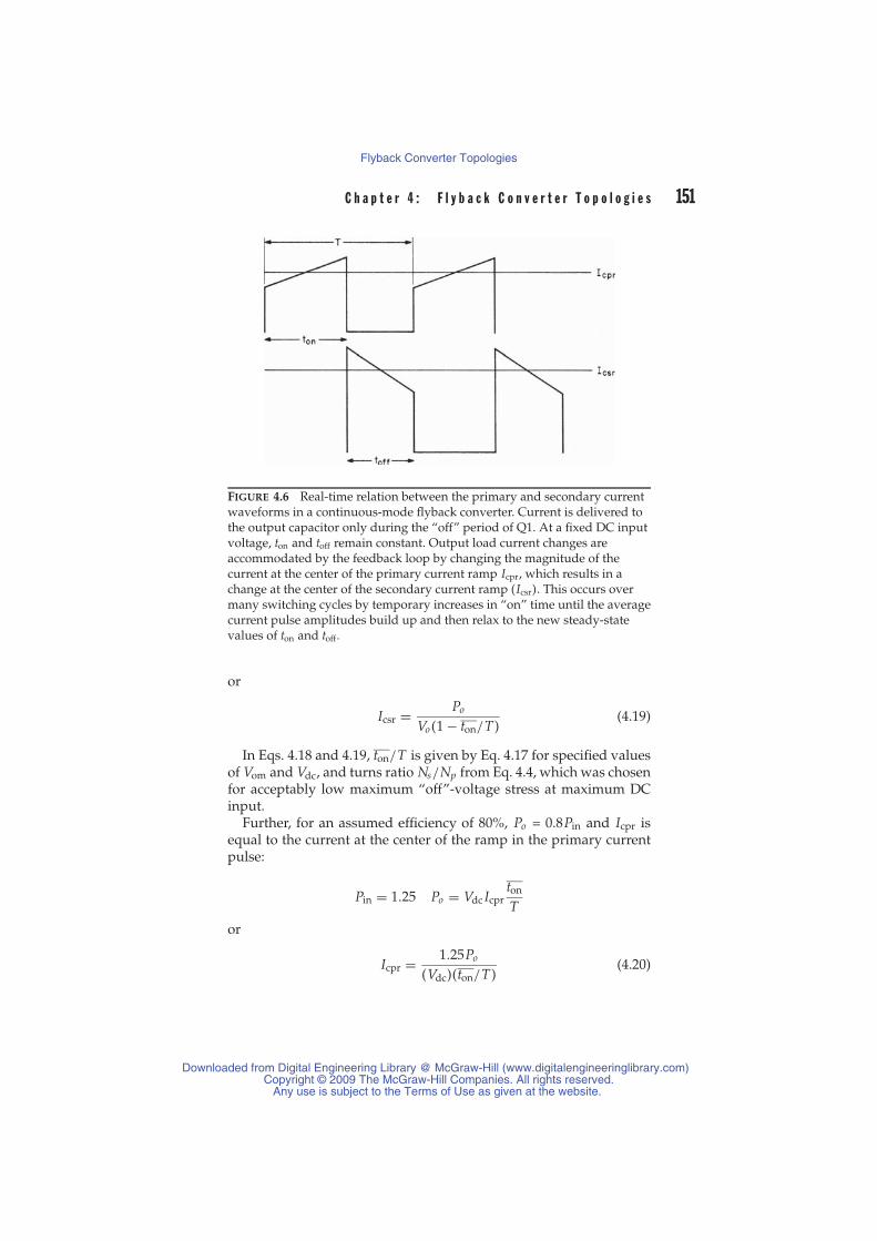
C h a p t e r 4 : F l y b a c k C o n v e r t e r T o p o l o g i e s 151
FIGURE 4.6 Real-time relation between the primary and secondary currentwaveforms in a continuous-mode flyback converter. Current is delivered tothe output capacitor only during the “off” period of Q1. At a fixed DC inputvoltage, ton and toff remain constant. Output load current changes areaccommodated by the feedback loop by changing the magnitude of thecurrent at the center of the primary current ramp Icpr, which results in achange at the center of the secondary current ramp (Icsr). This occurs overmany switching cycles by temporary increases in “on” time until the averagecurrent pulse amplitudes build up and then relax to the new steady-statevalues of ton and toff.
or
Icsr = Po
Vo (1 − ton/T)(4.19)
In Eqs. 4.18 and 4.19, ton/T is given by Eq. 4.17 for specified valuesof Vom and Vdc, and turns ratio Ns/Np from Eq. 4.4, which was chosenfor acceptably low maximum “off”-voltage stress at maximum DCinput.
Further, for an assumed efficiency of 80%, Po = 0.8Pin and Icpr isequal to the current at the center of the ramp in the primary currentpulse:
Pin = 1.25 Po = Vdc Icprton
T
or
Icpr = 1.25Po
(Vdc)(ton/T)(4.20)
Downloaded from Digital Engineering Library @ McGraw-Hill (www.digitalengineeringlibrary.com)Copyright © 2009 The McGraw-Hill Companies. All rights reserved.
Any use is subject to the Terms of Use as given at the website.
Flyback Converter Topologies
152 S w i t c h i n g P o w e r S u p p l y D e s i g n
After Pressman In the continuous mode, the duty cycle is defined by thevoltage ratio. Changes in load current try to reflect into the primary, but fortransient load changes, the transformer inductance limits the rate of changeof current. Hence the first and immediate effect of a transient load increaseis to cause a decrease in output voltage, resulting in an increase in the “on”period of Q1 (to increase the primary current). But this results in a furtherdrop in output voltage because there is an immediate decrease in the energy-transferring “off” period (the secondary conducting period). It takes manycycles before the new higher current conditions are established, at which pointthe duty cycle returns to its original value. This is a dynamic effect intrinsicto the topology and cannot be compensated by the control loop. In terms ofcontrol theory, this translates to a right-half-plane-zero. ∼K.B.
4.8.3 Ramp Amplitudes for Continuous Modeat Minimum DC Input
It has been shown that the threshold of continuous-mode operationoccurs when there is just the beginning of a step at the front end of theprimary current ramp. Referring to Figure 4.6, the step appears whenthe current at the center of the primary ramp Icpr just exceeds half theramp amplitude dIp . That value of Icpr( Icpr) is then the minimum valueat which the circuit is still in the continuous mode. From Eq. 4.20, Icpris proportional to output power and hence for the minimum outputpower Po corresponding to Icpr
Icpr = dIp
2= 1.25Po
(Vdc)(ton/T)
or
dIp = 2.5Po
(Vdc)(ton/T)(4.21)
In Eq. 4.21, ton is taken from Eq. 4.17 at the corresponding valueminimum of Vdc(Vdc). The slope of the ramp dIp is given by d Ip =(Vdc − 1)ton/L p , where L p is the primary magnetizing inductance.Then
L p = (Vdc − 1)ton
d Ip
= (Vdc − 1)(Vdc)(ton)2
2.5Po T
(4.22)
Here again, Po is the minimum specified value of output powerand ton is the maximum “on” time calculated from Eq. 4.17 at theminimum specified DC input voltage Vdc.
Downloaded from Digital Engineering Library @ McGraw-Hill (www.digitalengineeringlibrary.com)Copyright © 2009 The McGraw-Hill Companies. All rights reserved.
Any use is subject to the Terms of Use as given at the website.
Flyback Converter Topologies

C h a p t e r 4 : F l y b a c k C o n v e r t e r T o p o l o g i e s 153
4.8.4 Discontinuous- and Continuous-ModeFlyback Design Example
It is instructive to compare discontinuous- and continuous-mode fly-back designs at the same output power levels and input voltages. Themagnitudes of the currents and primary inductances will be revealing.
Assume a 50-W, 5-V output flyback converter operating at 50 kHzfrom a telephone industry prime power source (38 V DC minimum,60 V maximum). Assume a minimum output power of one-tenth thenominal, or 5 W.
Consider first a discontinuous-mode flyback. Choosing a bipolartransistor with a 150-V Vceo rating is very conservative, because it is notnecessary to rely on the Vcer or Vcev ratings that permit larger voltages.Then in Eq. 4.4, assume that the maximum “off”-voltage stress Vmswithout a leakage spike is 114 V, which permits a 36-V leakage spikebefore the Vceo limit is reached. Then Eq. 4.4 gives Np/Ns = (114 −60)/6 = 9.
Eq. 4.7 gives the maximum “on” time as
ton = 6 × 9 × 0.820 × 10−6
37 + 6 × 9
= 9.49 μs
and primary inductance for Ro = 5/10 = 0.5 � from Eq. 4.8 is
L p = 0.52.5 × 20−6
(38 × 9.49
5
)2
× 10−12
= 52 μH
Peak primary current from Eq. 4.9 is
Ip = 38 × 9.49 × 10−6
52 × 10−6
= 6.9 A
and the start of the secondary current triangle is
Is(peak) = (Np/Ns) Ip = 9 × 6.9 = 62 A
Recall that in the discontinuous flyback, the reset time Tr—the time forthe secondary current to decay back to zero—plus the maximum “on”time is equal to 0.8T (Eq. 4.6). Reset time is then Tr = (0.8×20)−9.49 =6.5 μs, and the average value of the secondary current triangle (which
Downloaded from Digital Engineering Library @ McGraw-Hill (www.digitalengineeringlibrary.com)Copyright © 2009 The McGraw-Hill Companies. All rights reserved.
Any use is subject to the Terms of Use as given at the website.
Flyback Converter Topologies

154 S w i t c h i n g P o w e r S u p p l y D e s i g n
should equal the DC output current) is
I (secondary average) = Is(peak)
2Tr
T
=(
622
)6.520
= 10 A
which is the DC output current.Now consider a continuous-mode flyback for the same frequency,
input voltages, output power, output voltage, and the same Np/Nsratio of 9. From Eq. 4.17b, calculate ton/T for Vdc = 38 V as
5 =[
(37/9)(ton/T1 − ton/T
]− 1
or ton/T = 0.5934 and ton = 11.87 μs, toff = 8.13 μs and from Eq. 4.19
Icsr = 50(5)(1 − 0.5934)
= 24.59 A
and the average of the secondary current pulse, which should equalthe DC output current, is
I (secondary average) = Icsr(toff/T) = 24.59 × 8.13/20 = 10.0 A
which checks. From Eq. 4.20, Icpr = 1.25×50/(38)(11.86/20) = 2.77 A.From Eq. 4.22, for the minimum input power of 5 W at the minimum
DC input voltage of 38 V, L p = 37 × 38(11.86)2 × 10⁻¹²/2.5 × 5 × 20 ×10−6 = 791 μH.
The contrast between the discontinuous and continuous modes willnow be clear from the following table, which compares the requiredprimary inductances, and primary and secondary currents at mini-mum DC input of 38 V.
Discontinuous ContinuousPrimary inductance, μH 52 791
Primary peak current, A 6.9 2.77
Secondary peak current, A 62.0 24.6
On time, μs 9.49 11.86
Off time, μs 6.5 8.13
The lower primary current and especially the secondary current forthe continuous mode are certainly an advantage, but the much largerprimary inductance that slows up response to load current changes,and the right-half-plane-zero that requires a very low error-amplifier
Downloaded from Digital Engineering Library @ McGraw-Hill (www.digitalengineeringlibrary.com)Copyright © 2009 The McGraw-Hill Companies. All rights reserved.
Any use is subject to the Terms of Use as given at the website.
Flyback Converter Topologies
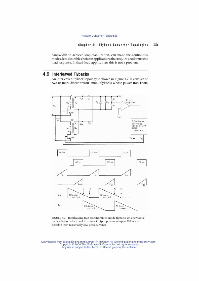
C h a p t e r 4 : F l y b a c k C o n v e r t e r T o p o l o g i e s 155
bandwidth to achieve loop stabilization, can make the continuousmode a less desirable choice in applications that require good transientload response. In fixed-load applications this is not a problem.
4.9 Interleaved FlybacksAn interleaved flyback topology is shown in Figure 4.7. It consists oftwo or more discontinuous-mode flybacks whose power transistors
FIGURE 4.7 Interleaving two discontinuous-mode flybacks on alternativehalf cycles to reduce peak currents. Output powers of up to 300 W arepossible with reasonably low peak currents.
Downloaded from Digital Engineering Library @ McGraw-Hill (www.digitalengineeringlibrary.com)Copyright © 2009 The McGraw-Hill Companies. All rights reserved.
Any use is subject to the Terms of Use as given at the website.
Flyback Converter Topologies

156 S w i t c h i n g P o w e r S u p p l y D e s i g n
are turned “on” at alternate half cycles and whose secondary currentsare summed through their rectifying diodes.
It can be used at power levels up to 300 W, limited mainly by thehigh-peak primary and especially secondary currents. Although thatpower level can be obtained with a single continuous-mode flybackwith reasonable currents, it may be better to accept the greater costand volume of two or more interleaved discontinuous-mode flybacks.Both input and output ripple currents are much smaller and of higherfrequency. Increasing the number of elements with suitable phase shiftbetween drive pulses will further reduce the ripple current. Further,the discontinuous mode’s faster response to load current changes,greater error-amplifier bandwidth, and the elimination of the right-half-plane-zero loop stabilization problem may make this a preferredchoice.
A single discontinuous-mode flyback at the 300-W level is imprac-tical because of the very high peak primary and secondary currents,as can be seen from Eqs. 4.2, 4.7, and 4.8.
At a lower power of 150 W, a single forward converter is very likelya better choice than the two interleaved flybacks because of the con-siderably lower secondary peak current of the forward converter. Theinterleaved flyback has been shown here for the sake of completenessand for its possible use at lower power levels when many (over five)outputs are required.
4.9.1 Summation of Secondary Currentsin Interleaved Flybacks
The magnetics design of each flyback in an interleaved flyback pro-ceeds exactly as for a single flyback at half the power level, because thesecondary currents add into the output through their “ORing” rectifierdiodes.
Even when both secondary diodes dump current simultaneously(as from t1 to t2), there is no possibility that one diode can back-bias theother and supply all the load current. This can happen if one attemptsto sum the currents of two low-impedance voltage sources. If one ofthe low-impedance voltage sources has a slightly higher open-circuitvoltage or a lower forward-drop OR diode, it will back-bias the otherdiode and supply all the load current by itself. This can over-dissipatethe diode or the transistor supplying that diode.
Looking back into the secondary of a flyback, however, there isa high-impedance current source, which is the secondary induc-tance. Thus the current dumped into the common load by eitherdiode is unaffected by the other diode simultaneously supplying loadcurrent.
Downloaded from Digital Engineering Library @ McGraw-Hill (www.digitalengineeringlibrary.com)Copyright © 2009 The McGraw-Hill Companies. All rights reserved.
Any use is subject to the Terms of Use as given at the website.
Flyback Converter Topologies
C h a p t e r 4 : F l y b a c k C o n v e r t e r T o p o l o g i e s 157
4.10 Double-Ended (Two Transistor)Discontinuous-Mode Flyback
4.10.1 Area of ApplicationThe topology is shown in Figure 4.8a . Its major advantage is that, usingthe scheme of the double-ended forward converter of Figure 2.13, itspower transistors in the “off” state are subjected to only the maximumDC input voltage. This is a significant advantage over the single-endedforward converter of Figure 4.1, where the maximum “off”-voltagestress is the maximum DC input voltage plus the reflected secondaryvoltage (Np/Ns)(Vo + 1) plus a leakage inductance spike that may beas high as one-third of the DC input voltage.
4.10.2 Basic OperationThe lower “off”-voltage stress comes about in the same way as forthe double-ended forward converter of Figure 2.13. Power transis-tors Q1, Q2 are turned “on” simultaneously. When they are “on,” thedot end of the secondary is negative, D3 is reverse-biased, and nosecondary current flows. The primary is then just an inductor, andcurrent in it ramps up linearly at a rate of dI1/dt = Vdc/(Lm + Ll ),where Lm and Ll are the primary magnetizing and leakage induc-tances, respectively. When Q1 and Q2 turn “off,” as in the previousflybacks, all primary and secondary voltages reverse polarity, D3 be-comes forward-biased, and the stored energy in Lm = 1/2Lm( I1)2 isdelivered to the load.
As shown previously, the “on” or set volt-second product acrossthe primary must equal the “off” or reset volt-second product. At theinstant of turn “off,” the bottom end of Ll attempts to go far positivebut is clamped to the positive end of Vdc. The top end of Lm attemptsto go far negative but is clamped to the negative end of Vdc. Thusthe maximum voltage stress at either Q1 or Q2 can never be morethan Vdc.
The actual resetting voltage Vr across the magnetizing inductanceLm during the “off” time is given by the voltage reflected from thesecondary (Np/Ns)(Vo + VD3). The voltage across Lm and Ll in seriesis the DC supply voltage, and hence, as seen in Figure 4.8b, the voltageacross the leakage inductance Ll is Vl = (Vdc − Vr ).
The division of the Vdc supply voltage across Lm and Ll in seriesduring the “off” time is a very important point in the circuit designand establishes the transformer turns ratio Np/Ns as discussed below.
The price paid for this advantage is, of course, the requirement fortwo transistors and the two clamp diodes, D1, D2.
Downloaded from Digital Engineering Library @ McGraw-Hill (www.digitalengineeringlibrary.com)Copyright © 2009 The McGraw-Hill Companies. All rights reserved.
Any use is subject to the Terms of Use as given at the website.
Flyback Converter Topologies
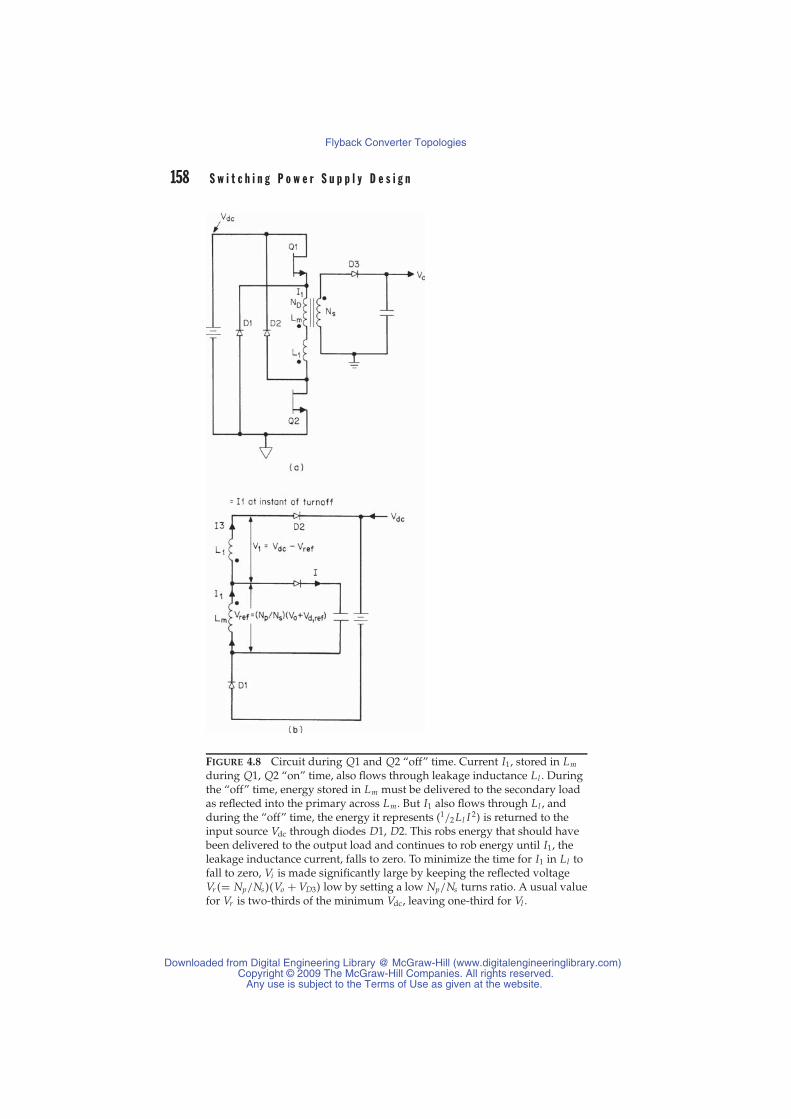
158 S w i t c h i n g P o w e r S u p p l y D e s i g n
FIGURE 4.8 Circuit during Q1 and Q2 “off” time. Current I1, stored in Lm
during Q1, Q2 “on” time, also flows through leakage inductance Ll . Duringthe “off” time, energy stored in Lm must be delivered to the secondary loadas reflected into the primary across Lm. But I1 also flows through Ll , andduring the “off” time, the energy it represents (1/2 Ll I 2) is returned to theinput source Vdc through diodes D1, D2. This robs energy that should havebeen delivered to the output load and continues to rob energy until I1, theleakage inductance current, falls to zero. To minimize the time for I1 in Ll tofall to zero, Vi is made significantly large by keeping the reflected voltageVr (= Np/Ns )(Vo + VD3) low by setting a low Np/Ns turns ratio. A usual valuefor Vr is two-thirds of the minimum Vdc, leaving one-third for Vl .
Downloaded from Digital Engineering Library @ McGraw-Hill (www.digitalengineeringlibrary.com)Copyright © 2009 The McGraw-Hill Companies. All rights reserved.
Any use is subject to the Terms of Use as given at the website.
Flyback Converter Topologies
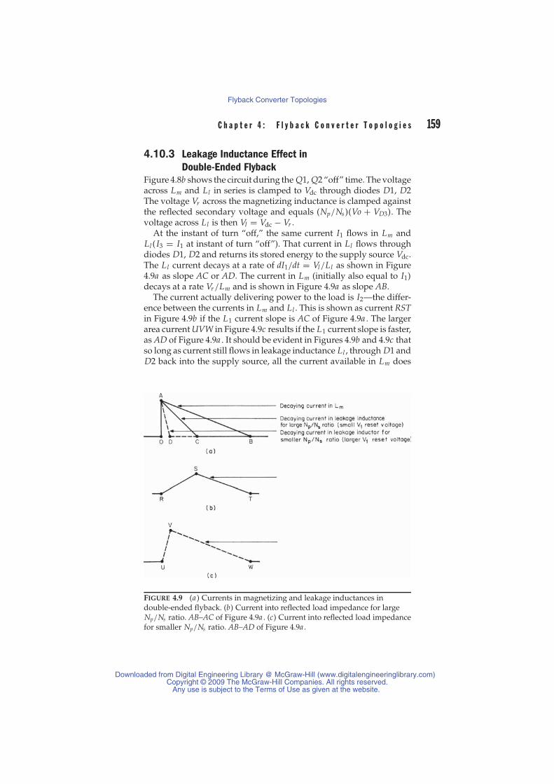
C h a p t e r 4 : F l y b a c k C o n v e r t e r T o p o l o g i e s 159
4.10.3 Leakage Inductance Effect inDouble-Ended Flyback
Figure 4.8b shows the circuit during the Q1, Q2 “off” time. The voltageacross Lm and Ll in series is clamped to Vdc through diodes D1, D2The voltage Vr across the magnetizing inductance is clamped againstthe reflected secondary voltage and equals (Np/Ns)(Vo + VD3). Thevoltage across Ll is then Vl = Vdc − Vr .
At the instant of turn “off,” the same current I1 flows in Lm andLl ( I3 = I1 at instant of turn “off”). That current in Ll flows throughdiodes D1, D2 and returns its stored energy to the supply source Vdc.The Ll current decays at a rate of dI1/dt = Vl/Ll as shown in Figure4.9a as slope AC or AD. The current in Lm (initially also equal to I1)decays at a rate Vr/Lm and is shown in Figure 4.9a as slope AB.
The current actually delivering power to the load is I2—the differ-ence between the currents in Lm and Ll . This is shown as current RSTin Figure 4.9b if the L1 current slope is AC of Figure 4.9a . The largerarea current UVW in Figure 4.9c results if the L1 current slope is faster,as AD of Figure 4.9a . It should be evident in Figures 4.9b and 4.9c thatso long as current still flows in leakage inductance Ll , through D1 andD2 back into the supply source, all the current available in Lm does
FIGURE 4.9 (a ) Currents in magnetizing and leakage inductances indouble-ended flyback. (b) Current into reflected load impedance for largeNp/Ns ratio. AB–AC of Figure 4.9a . (c) Current into reflected load impedancefor smaller Np/Ns ratio. AB–AD of Figure 4.9a .
Downloaded from Digital Engineering Library @ McGraw-Hill (www.digitalengineeringlibrary.com)Copyright © 2009 The McGraw-Hill Companies. All rights reserved.
Any use is subject to the Terms of Use as given at the website.
Flyback Converter Topologies

160 S w i t c h i n g P o w e r S u p p l y D e s i g n
not flow into the reflected load but is partly diverted back into thesupply.
It can thus be seen from Figures 4.9b and 4.9c that to maximize thetransfer of Lm current to the reflected load and to avoid a delay in thetransfer of current to the load, the slope of the leakage inductance cur-rent decay should be maximized (slope AD rather than AC in Figure4.9a ). Or in magnetics–power supply jargon, the leakage inductancecurrent should be rapidly reset to zero.
Since the rate of decay of the leakage inductance current is Vl/Lland Vl = Vdc − (Np/Ns)(Vo + VD3), choosing lower values of Np/Nsincreases Vl and hastens leakage current reset. A usual value for thereflected voltage (Np/Ns)(Vo + VD3) is two-thirds of Vdc, leaving one-third for Vl . Too low a value for Vr will require a longer time to resetthe magnetizing inductance, rob from the available Q1, Q2 “on” time,and decrease the available output power.
Once Np/Ns has been fixed to yield Vl = Vdc/3, the maximum“on” time for discontinuous operation is calculated from Eq. 4.7, Lmis calculated from Eq. 4.8 and Ip from Eq. 4.9, just as for the single-ended flyback.
References1. Billings, K., Switchmode Power Supply Handbook, McGraw-Hill, New York, 1989.2. Chryssis, G., High Frequency Switching Power Supplies, 2nd Ed., McGraw-Hill,
New York, 1989, pp. 122–131.3. Dixon, L., “The Effects of Leakage Inductance on Multi-output Flyback
Circuits,” Unitrode Power Supply Design Seminar Handbook, Unitrode Corp.,Lexington, Mass., 1988.
4. Patel, R., D. Reilly, and R. Adair, “150 Watt Flyback Regulator,” Unitrode PowerSupply Design Seminar Handbook, Unitrode Corp., Lexington, Mass., 1988.
Downloaded from Digital Engineering Library @ McGraw-Hill (www.digitalengineeringlibrary.com)Copyright © 2009 The McGraw-Hill Companies. All rights reserved.
Any use is subject to the Terms of Use as given at the website.
Flyback Converter Topologies

C H A P T E R 5Current-Mode and
Current-Fed Topologies
5.1 IntroductionIn this chapter, current-mode1–7 and current-fed9–20 topologies aregrouped into one family, despite their very significant differences,because they both rely on controlling input current and output voltage.However, they do this in quite different ways.
5.1.1 Current-Mode ControlCurrent-mode control (Figure 5.3) has two control loops: a slow outerloop (via R1,R2 and error amp EA), which senses DC output voltageand delivers a control voltage (Veao), to a much faster inner currentcontrol loop (via R1, Vi , and the pulse width modulator PWM). Risenses peak transistor currents (the peak choke current) and keepsthe peak current constant on a pulse-by-pulse basis. The end result isthat it solves the magnetic flux imbalance problem in the current-modeversion of the push-pull topology and restores push-pull as a viableapproach in applications where the uncertainty of other solutions toflux imbalance is a drawback (Section 2.2.8). Further, the constantpower transistor current pulses simplify the feedback-loop design.
After Pressman Because the converter in this example is a forward type,the secondary current reflects back into the primary. By sensing the current inthe common return of Q1 and Q2, the inner current control loop effectivelyis looking at the current flow in the output choke Lo . The fast inner loopmaintains the peak current in Lo constant on a pulse-by-pulse basis, changingonly slowly in response to voltage adjustments. In this way, the peak outputcurrent in Lo is the controlled parameter. This takes Lo out of the small signaltransfer function of the outer loop, allowing faster response in the closed loopsystem. At the same time, because current is the controlled parameter, current
161Downloaded from Digital Engineering Library @ McGraw-Hill (www.digitalengineeringlibrary.com)
Copyright © 2009 The McGraw-Hill Companies. All rights reserved.Any use is subject to the Terms of Use as given at the website.
Source: Switching Power Supply Design

162 S w i t c h i n g P o w e r S u p p l y D e s i g n
limit and short circuit protection are intrinsic in the topology. Further, sincecurrent is controlled on a pulse-by-pulse basis, any tendency for currentimbalance in Q1 and Q1 is eliminated and staircase saturation of T1 is nolonger a possibility. Finally, the effect of any changes in supply voltage isautomatically eliminated from the peak output current in Lo , so that lineregulation is automatically better. ∼K.B.
5.1.2 Current-Fed TopologyA current-fed topology derives its input current from an input induc-tor (choke) as shown in Figure 5.9. In this example, the top end of apush-pull forward converter transformer gets its supply from inputinductor L1. Thus the power train is driven from the high impedancecurrent source (the input inductor L1) rather than the low impedanceof a rectifier filter capacitor or perhaps the low-source impedance ofa source battery. This higher source impedance helps to solve the fluximbalance problem in T1 and offers other significant advantages.
5.2 Current-Mode ControlIn all the voltage-mode topologies discussed so far, output voltagealone is the controlled parameter. In those circuits, regulation againstload current changes occurs because current changes cause small out-put voltage changes that are sensed by a voltage-monitoring erroramplifier, which then corrects the power transistor “on” time to main-tain output voltage constant. Output current itself is not monitoreddirectly.
In the 1980s, the new topology current-mode control appeared, inwhich both voltage and current were monitored. The scheme hadbeen known previously, but was not widely used as it required dis-crete circuit components to implement it. When a new Unitrode™pulse-width-modulating (PWM) chip—the UC1846—appeared, withall the features needed to implement current-mode control, the ad-vantages of the technique were quickly recognized and it was widelyadopted.
After Pressman As of 2008, many similar current-mode control ICs arenow available. Unitrode is now part of Texas Instruments. ∼K.B.
Where two 180o out-of-phase width-modulated drive signals arerequired as in the push-pull, half-bridge, full-bridge, interleaved for-ward converter, or flyback, the UC1846 can be used to implementcurrent-mode control. A lower-cost, single-ended PWM controller,the UC1842, is currently available to implement current mode in
Downloaded from Digital Engineering Library @ McGraw-Hill (www.digitalengineeringlibrary.com)Copyright © 2009 The McGraw-Hill Companies. All rights reserved.
Any use is subject to the Terms of Use as given at the website.
Current-Mode and Current-Fed Topologies

C h a p t e r 5 : C u r r e n t - M o d e a n d C u r r e n t - F e d T o p o l o g i e s 163
single-ended circuits such as forward converters, flybacks, and buckregulators.
5.2.1 Current-Mode Control Advantages5.2.1.1 Avoidance of Flux Imbalance in Push-Pull ConvertersFlux imbalance was discussed in Section 2.2.5. It occurs in a push-pullconverter when the transformer core operates asymmetrically aboutthe origin of its hysteresis loop. The consequence is that the core movesup toward saturation and one transistor draws more current duringits “on” time than does the opposite transistor (Figure 2.4c).
As the core drifts further off center of the origin, it goes deeply intosaturation and may destroy the power transistor. A number of ways tocope with flux imbalance have been described in Section 2.2.8. Theseschemes work, but under unusual line or load transient conditions andespecially at higher output powers, there is never complete certaintythat flux imbalance cannot occur.
Current-mode monitors current on a pulse-by-pulse basis andforces alternate pulses to have equal peak amplitudes by correctingeach transistor’s “on” time so that current amplitudes must be equal.This puts push-pull back into the running in any proposed new designand is a valuable contribution to the repertoire of possible topologies.For example, if a forward converter with no flux imbalance problemwere chosen to be certain of no flux imbalance in the absence of currentmode, a severe penalty would be paid.
Eq. 2.28 shows the peak primary current in a forward converteris 3.13( Po/Vdc). But Eq. 2.9 shows it is only half that or 1.56( Po/Vdc)for the push-pull. At low output powers, it is not a serious drawbackto use the forward converter with twice the peak current of a push-pull at equal output power, especially since the forward converterhas only one transistor. But at higher output power, twice the peakprimary current in a forward converter than in a push-pull becomesprohibitive.
The push-pull is a very attractive choice for telephone industrypower supplies where the maximum DC input voltage is specified asonly 38–60 V. Having it in its current-mode version with a certaintythat flux imbalance cannot exist is very valuable.
5.2.1.2 Fast Correction Against Line Voltage ChangesWithout Error Amplifier Delay (Voltage Feed-Forward)
It is inherent in the details of how current mode works that a line volt-age change immediately causes a change in power transistor “on”time. This change is corrected without having to wait for an out-put voltage change to be sensed after a relatively long delay by a
Downloaded from Digital Engineering Library @ McGraw-Hill (www.digitalengineeringlibrary.com)Copyright © 2009 The McGraw-Hill Companies. All rights reserved.
Any use is subject to the Terms of Use as given at the website.
Current-Mode and Current-Fed Topologies

164 S w i t c h i n g P o w e r S u p p l y D e s i g n
conventional voltage error amplifier. The details of how this comesabout will be discussed below.
5.2.1.3 Ease and Simplicity of Feedback-Loop StabilizationAll the topologies discussed above with the exception of flybacks havean output LC filter. An LC filter has a maximum possible phase shiftof 180o not far above its resonant frequency of fo = 1
2π√
LC, and gain
between input and output falls very rapidly with increasing frequency.As frequency increases, the impedance of the series L arm increasesand that of the shunt arm decreases.
This possible large phase shift and rapid change of gain with fre-quency complicates feedback-loop design. More important, the ele-ments around the error amplifier required to stabilize the loop aremore complex and can cause problems with rapid changes in inputvoltage or output current.
In a small-signal analysis of the current-mode outer voltage loop,however, which calculates gain and phase shift to consider the possi-bility of oscillation, the output inductor does not appear even thoughit is physically in series with the output shunt capacitor. So for smallsignal changes, the voltage loop behaves as if the inductor were notthere.
The circuit behaves as if there were a constant current feeding theparallel combination of the output capacitor and the output load resis-tor. Such a network can yield only 90o rather than 180o of phase shift,and the gain between input and output falls half as rapidly as for atrue LC filter (–20 dB per decade rather than –40 dB per decade). Thissimplifies feedback-loop design, simplifies the circuitry around theerror amplifier required for stabilization, and avoids problems aris-ing from rapid line or load changes. The details of why this is so willbe discussed below.
5.2.1.4 Paralleling OutputsA number of current-mode power supplies may be operated in paral-lel, each with an equal share of the total load current. This is achievedby sensing current in each supply with equal current sensing resistors,which convert transistor peak current pulses to voltage pulses. Theseare compared in a voltage comparator to a common error-amplifieroutput voltage, which forces peak current-sensing voltages and hencepeak currents in the parallel supplies to be equal.
5.2.1.5 Improved Load Current RegulationCurrent mode has better load current regulation than voltage mode.The improvement is not as great as that in voltage regulation, however,which is greatly enhanced by the feed-forward characteristic inherent
Downloaded from Digital Engineering Library @ McGraw-Hill (www.digitalengineeringlibrary.com)Copyright © 2009 The McGraw-Hill Companies. All rights reserved.
Any use is subject to the Terms of Use as given at the website.
Current-Mode and Current-Fed Topologies

C h a p t e r 5 : C u r r e n t - M o d e a n d C u r r e n t - F e d T o p o l o g i e s 165
in current mode. The improved load current regulation comes aboutbecause of the greater error-amplifier bandwidth possible in currentmode.
5.3 Current-Mode vs. Voltage-ModeControl CircuitsTo understand the differences and advantages of current mode overvoltage mode, it is essential first to see how voltage-mode control cir-cuitry works. The basic elements of a typical voltage-mode, PWM con-trol circuit are shown in Figure 5.1. That block diagram shows most ofthe elements of the SG1524, the first of many integrated-circuit controlchips that have revolutionized the switching power supply industry.The SG1524, originally made by Silicon General Corporation, is nowmanufactured by many other companies and in improved versionssuch as the UC1524A (Unitrode) and SG1524B (Silicon General).
5.3.1 Voltage-Mode Control CircuitryIn Figure 5.1, an oscillator generates a 3-V sawtooth Vst. The DC volt-age at the triangle base is about 0.5 V and, at the peak, about 3.5 V.The period of the sawtooth is set by external discrete components Rtand Ct and is approximately equal to T = RtCt .
An error amplifier compares a fraction of the output voltage KVoto a voltage reference Vref and produces an error voltage Vea. Vea iscompared to the sawtooth Vst in a voltage comparator (PWM). Notethat the fraction of the output KVo is fed to the inverting input of theerror amplifier so that when Vo goes up, the error-amplifier output Veagoes down.
In the PWM voltage comparator, the sawtooth is fed to the non-inverting input and Vea is fed to the inverting input. Thus the PWMoutput is a negative-going pulse of variable width. The pulse is neg-ative for the entire time the sawtooth is below the DC level of theerror-amplifier output Vea or from t1 to t2. As the DC output voltagegoes—say—slightly positive, KVo goes slightly positive, and Vea goesnegative and closer to the bottom of the sawtooth. Thus the durationof the negative-going pulse Vpwm decreases.
The duration of this negative-going pulse is the duration of thepower transistor “on” time. Further, since in all the voltage-modetopologies discussed above, the DC output voltage is proportionalto the power transistor “on” time, decreasing the “on” time bringsthe DC output voltage back down by negative-feedback loop action.The duration of the negative pulse Vpwm increases as the output DCvoltage decreases.
Downloaded from Digital Engineering Library @ McGraw-Hill (www.digitalengineeringlibrary.com)Copyright © 2009 The McGraw-Hill Companies. All rights reserved.
Any use is subject to the Terms of Use as given at the website.
Current-Mode and Current-Fed Topologies
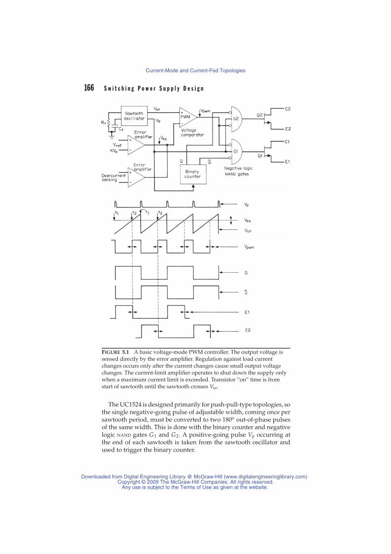
166 S w i t c h i n g P o w e r S u p p l y D e s i g n
FIGURE 5.1 A basic voltage-mode PWM controller. The output voltage issensed directly by the error amplifier. Regulation against load currentchanges occurs only after the current changes cause small output voltagechanges. The current-limit amplifier operates to shut down the supply onlywhen a maximum current limit is exceeded. Transistor “on” time is fromstart of sawtooth until the sawtooth crosses Vea.
The UC1524 is designed primarily for push-pull-type topologies, sothe single negative-going pulse of adjustable width, coming once persawtooth period, must be converted to two 180o out-of-phase pulsesof the same width. This is done with the binary counter and negativelogic NAND gates G1 and G2. A positive-going pulse Vp occurring atthe end of each sawtooth is taken from the sawtooth oscillator andused to trigger the binary counter.
Downloaded from Digital Engineering Library @ McGraw-Hill (www.digitalengineeringlibrary.com)Copyright © 2009 The McGraw-Hill Companies. All rights reserved.
Any use is subject to the Terms of Use as given at the website.
Current-Mode and Current-Fed Topologies

C h a p t e r 5 : C u r r e n t - M o d e a n d C u r r e n t - F e d T o p o l o g i e s 167
Outputs from the binary counter Q and Q̄ are then out-of-phasesquare waves at half the sawtooth frequency. When they are negative,these square waves steer negative Vpwm pulses alternately throughnegative logic NAND G1 and G2. These gates produce a positive outputonly for the duration of time that the inputs are negative. Thus thebases (and emitters) of output transistors Q1 and Q2 are positive onlyon alternate half cycles and only for the same duration as the Vpwmnegative pulses.
The “on” time of the power transistors must correspond to thetime the Vpwm pulse is negative for the complete circuit to havenegative feedback, since KVo is connected to the inverting termi-nal of the error amplifier. Thus if the power transistors are of theNPN type, they must be fed from the emitters of Q1, Q2, or if ofthe PNP type, from the collectors. If current amplifiers are inter-posed between the bases of the output transistors and Q1, Q2, po-larities must be such that Q1, Q2 are “on” when the output transistorsare “on.”
The narrow positive pulse Vp is fed directly into gates G1, G2. Thisforces both gate outputs to be “low” simultaneously for the dura-tion of Vp , and both output transistors to be “off” for that duration.This ensures that if the pulse width of Vpwm ever approached a fullhalf period, both power transistors could never be “on” simultane-ously at the end of the half period. In a push-pull topology, if bothtransistors are simultaneously “on” even for a short time, they aresubjected to both high current and the full supply voltage and couldbe destroyed.
This, then, is a voltage-mode circuit. Power transistor or outputcurrent is not sensed directly. The power transistors are turned “on” atthe beginning of a half period and turned “off” when the sawtooth Vstcrosses the DC level of the error-amplifier output, which is a measureof output voltage only.
The complete details of the SG1524 are shown in Figure 5.2a . Thenegative logic NAND gates G1, G2 of Figure 5.1 are shown in Figure 5.2aas positive logic NOR gates. These perform the same function for re-quiring all “lows” to make a “high” and are identical to any one “high”forcing a “low.”
In Figure 5.2a , when pin 10 goes “high,” the associated transis-tor collector goes “low” and brings the error-amplifier output (pin 9)down to the base of the sawtooth. This reduces output transistor “on”times to zero and shuts down the supply. In the current limit com-parator, if pin 4 is 200 mV more positive than pin 5, the error-amplifieroutput is also brought down to ground (there is an internal phase in-version, not shown) and the supply is shut down. Pins 4 and 5 arebridged across a current-sensing resistor in series with the currentbeing monitored. If current is to be limited to Im, the resistor is se-lected as Rs = 0.2/Im.
Downloaded from Digital Engineering Library @ McGraw-Hill (www.digitalengineeringlibrary.com)Copyright © 2009 The McGraw-Hill Companies. All rights reserved.
Any use is subject to the Terms of Use as given at the website.
Current-Mode and Current-Fed Topologies
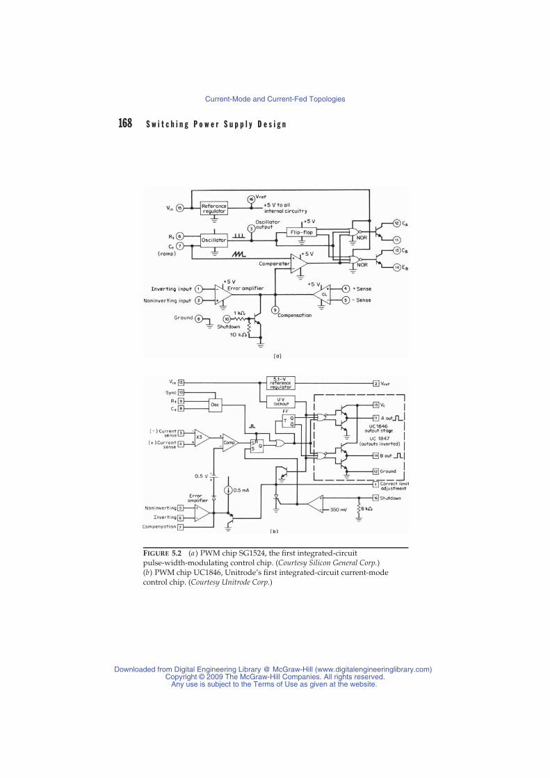
168 S w i t c h i n g P o w e r S u p p l y D e s i g n
FIGURE 5.2 (a ) PWM chip SG1524, the first integrated-circuitpulse-width-modulating control chip. (Courtesy Silicon General Corp.)(b) PWM chip UC1846, Unitrode’s first integrated-circuit current-modecontrol chip. (Courtesy Unitrode Corp.)
Downloaded from Digital Engineering Library @ McGraw-Hill (www.digitalengineeringlibrary.com)Copyright © 2009 The McGraw-Hill Companies. All rights reserved.
Any use is subject to the Terms of Use as given at the website.
Current-Mode and Current-Fed Topologies
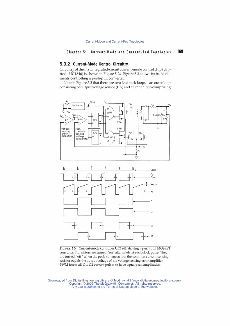
C h a p t e r 5 : C u r r e n t - M o d e a n d C u r r e n t - F e d T o p o l o g i e s 169
5.3.2 Current-Mode Control CircuitryCircuitry of the first integrated-circuit current-mode control chip (Uni-trode UC1846) is shown in Figure 5.2b. Figure 5.3 shows its basic ele-ments controlling a push-pull converter.
Note in Figure 5.3 that there are two feedback loops—an outer loopconsisting of output voltage sensor (EA) and an inner loop comprising
FIGURE 5.3 Current-mode controller UC1846, driving a push-pull MOSFETconverter. Transistors are turned “on” alternately at each clock pulse. Theyare turned “off” when the peak voltage across the common current-sensingresistor equals the output voltage of the voltage-sensing error amplifier.PWM forces all Q1, Q2 current pulses to have equal peak amplitudes.
Downloaded from Digital Engineering Library @ McGraw-Hill (www.digitalengineeringlibrary.com)Copyright © 2009 The McGraw-Hill Companies. All rights reserved.
Any use is subject to the Terms of Use as given at the website.
Current-Mode and Current-Fed Topologies

170 S w i t c h i n g P o w e r S u p p l y D e s i g n
primary peak current sensor (PWM) and current-sensing resistor Riwhich converts ramp-on-a-step transistor currents to ramp-on-a-stepvoltages.
Line and load current changes are regulated by varying power tran-sistor “on” time. “On” time is determined by both the voltage-sensingerror-amplifier output Veao and the PWM voltage comparator, whichcompares Veao to the ramp-on-a-step voltage at the top of the current-sensing resistor Ri .
Because the secondaries all have output inductors, the secondarycurrents have the characteristic ramp-on-a-step shape. These reflectas identical-shaped currents, which are smaller by the Ns/Np ratio,in the primary and the output transistors. Those currents flowing inthe common emitters through Ri produce the ramp-on-a-step voltagewaveshape Vi . Power transistor “on” time is then determined as fol-lows: An internal oscillator, whose period is set by external discretecomponents Rt , Ct , generates narrow clock pulses C p . The oscillatorperiod is approximately 0.9RtCt . At every clock pulse, feed-forwardFF1 is reset, causing its output Qpw to go “low.” The duration of the“low” time at Qpw, it will soon be seen, is the duration of the “high”time at either of the chip outputs A or B and, hence, the duration ofthe power transistor “on” times.
When the PWM voltage comparator output goes “high,” FF1 is set,thus terminating the Qpw “low” and hence the “high” time at A or B,and turns “off” the power transistor which had been “on.” Thus theinstant at which the PWM comparator output goes “high” determinesthe end of the “on” time.
The PWM comparator compares the ramp-on-a-step current-sensing voltage Vi to the output of the voltage error-amplifier EA.Hence when the peak of Vi equals Veao, the PWM output goes posi-tive and sets FF1, Qpw goes “high,” and whichever of Aor B had been“high” goes “low.” The power transistor that had just been “on” isnow turned “off.”
A “low” output from FF1 occurs once per clock period. It starts“low” at every clock pulse and goes back “high” when the PWM non-inverting input equals the DC level of the EA output. Most frequently,power transistors Q1, Q2 will be N types, which require positive-going signals for turn “on.” Thus these equal-duration negative-goingpulses are steered alternately through negative logic NAND gates G1and G2, becoming 180o out-of-phase, positive-going pulses at the chipoutputs A and B.
Chip output stages TPA and TPB are “totem poles.” When thebottom transistor of a totem pole is “on,” the top one is “off” andvice versa. Output nodes A and B have very low output impedance.When the bottom transistor is “on,” it can “sink” (absorb inward-directed current) 100 mA continuous and 400 mA during the “high”-to-“low” transition. When the top transistor is “on,” it can “source”
Downloaded from Digital Engineering Library @ McGraw-Hill (www.digitalengineeringlibrary.com)Copyright © 2009 The McGraw-Hill Companies. All rights reserved.
Any use is subject to the Terms of Use as given at the website.
Current-Mode and Current-Fed Topologies
C h a p t e r 5 : C u r r e n t - M o d e a n d C u r r e n t - F e d T o p o l o g i e s 171
(emit outward-directed current) 100 mA continuous and 400 mA dur-ing the “low”-to-“high” transition.
Steering is done by binary counter BC1, which is triggered onceper clock pulse on the leading edge of the pulse. The negative-goingQ pulses steer the negative Qpw pulses alternately through negativelogic NAND gates G1, G2. The chip outputs A and B are 180o out-of-phase positive pulses whose duration is the same as that of thenegative pulses Qpw.
Note that Qpw is positive from the end of the “on” time until thestart of the next turn “on.” This forces the bubble outputs of G1, G2“high” and brings points A and B both “low.” This “low” at bothpower transistor inputs during the dead time between the turn “off”of one transistor and the turn “on” of the other is a valuable feature. Itpresents a low impedance at the “off”-voltage level and prevents noisepickup from turning the power transistors “on” spuriously. While thebubble outputs of G1, G2 are both “high,” their no-bubble outputsare both “low,” and thus turn “off” the upper transistors of the totempoles TPA and TPB and avoid over-dissipating them.
It can be seen also that the narrow positive clock pulse is fed as athird input to NAND gates G1, G2. This makes bubble outputs from G1,G2 “high” and outputs A, B simultaneously “low” for the durationof the clock pulse. This guarantees that under fault conditions, if thecontroller attempts a full half period “on” time (Qpw “low” and eitherAor B “high” for a full half period), there will be a dead time betweenthe end of one “on” time and the start of the opposite “on” time. Thusthe power transistors can’t conduct simultaneously.
5.4 Detailed Explanation of Current-ModeAdvantages5.4.1 Line Voltage RegulationConsider how the controller regulates against line voltage changes.Assume that line voltage (and hence Vdc) goes up. As Vdc goes up, thepeak controlled secondary voltage will go up and after a delay in Lo , Vowill eventually go up. Since secondary DC voltages are proportionalto secondary winding peak voltages and power transistor “on” time,the “on” time must decrease because the peak secondary voltage hasincreased. Then, after a delay through the error amplifier, Veao will godown and, in the PWM comparator, the ramp in Vi will become equalto the lowered value of Veao earlier in time. Thus, “on” time will bedecreased and the output voltage will be brought back down.
If this were the only mechanism to correct against line voltagechanges, however, the correction would be slow due to the delays in
Downloaded from Digital Engineering Library @ McGraw-Hill (www.digitalengineeringlibrary.com)Copyright © 2009 The McGraw-Hill Companies. All rights reserved.
Any use is subject to the Terms of Use as given at the website.
Current-Mode and Current-Fed Topologies

172 S w i t c h i n g P o w e r S u p p l y D e s i g n
Lo and the error amplifier, but there is a shortcut around those delays.As Vdc goes up, the peak voltage at the input to the output inductor Vspincreases, the slope of inductor current DIs/ dt increases, and hencethe slope of the ramp of Vi increases. Now the faster ramp equals Veaoearlier in time, and the “on” time is shortened without having to waitfor Veao to move down and shorten the “on” time. Output voltage tran-sients resulting from input voltage transients are smaller in amplitudeand shorter in duration because of this feed-forward characteristic.
5.4.2 Elimination of Flux ImbalanceConsider the waveform Vi in Figure 5.3. It is taken from the current-sensing resistor Ri and is hence proportional to power transistor cur-rents. The “on” time ends when the peak of the ramp in Vi equals theoutput voltage of the error amplifier Veao. It can be seen in Figure 5.3that peak currents on alternate half cycles cannot be unequal as in Fig-ure 2.4b and 2.4c because the error-amplifier output Veao is essentiallyhorizontal and cannot change significantly within one cycle becauseof limited EA bandwidth.
If the transformer core got slightly off center and started walk-ing up into saturation on one side, the voltage Vi would becomeslightly concave upward close to the end of that “on” time. It wouldthen equal Veao earlier and terminate that “on” time sooner. Flux in-crease in that half cycle would then cease, and in the next half cycle,since the opposite transistor would not have a foreshortened “on”time, the core flux would be brought back down and away fromsaturation.
Since the peaks of the voltage ramps in Figure 5.3 (Vi ) are equal, peakcurrents on alternate half cycles must be equal. Thus the inequalityof alternate currents and flux imbalance shown in Figure 2.4b are notpossible.
5.4.3 Simplified Loop Stabilization fromElimination of Output Inductor inSmall-Signal Analysis
Refer to Figure 5.3. In a small-signal analysis to determine whetherthe outer voltage loop is stable, it is assumed that the loop is openedat some point and a small sinusoidal signal of variable frequency isinserted at the input side of the break. The gain and phase shift versusfrequency are calculated through all the loop elements starting fromthe input side of the break, around to the same point at the output sideof the loop break. By tailoring the error-amplifier gain and phase shiftproperly in relation to the other elements in the open loop (primarilythe output LC filter), the closed loop is made stable.
Downloaded from Digital Engineering Library @ McGraw-Hill (www.digitalengineeringlibrary.com)Copyright © 2009 The McGraw-Hill Companies. All rights reserved.
Any use is subject to the Terms of Use as given at the website.
Current-Mode and Current-Fed Topologies

C h a p t e r 5 : C u r r e n t - M o d e a n d C u r r e n t - F e d T o p o l o g i e s 173
The variable frequency is often inserted at the input to the erroramplifier. In Chapter 12 on feedback loop stability analysis, it will beshown how gain and phase shift through the error amplifier may becalculated and tailored to achieve the desired results.
Considering Figure 5.3, the concept of gain and phase shift of asinusoidal signal from the error-amplifier output to the input of theLC filter may not be obvious. Of primary importance is the fact that thehighest frequency to which the loop will respond significantly is wellbelow the switching frequency of the converter. The error-amplifieroutput Veao is, therefore, a slowly changing or essentially DC voltagethat, when it equals the peak of the ramp-on-a-step pulse sequence Vi ,results in a sequence of negative-going pulses at Qpw whose durationdepends on Veao. The Qpw negative pulses result in a sequence ofpositive-going pulses at the input to the LC filter.
It may seem puzzling to speak of gain and phase shift of sinusoidalsignals in view of this odd operation of converting a voltage level toa sequence of pulses at the switching frequency. The situation may beclarified as follows.
If there is a sinusoidal signal at the error-amplifier input, it is am-plified and phase-shifted at the EA output. Thus Veao is sinusoidallyamplitude modulated at that frequency. The Qpw negative pulses aresimilarly pulse width modulated at that frequency. So are the “on”times of the positive-going pulses at the output rectifiers pulse widthmodulated at that frequency. Hence, the voltage at the output recti-fier cathodes, which is proportional to the pulse widths, when aver-aged over a time long compared to the switching period, is simplyamplitude modulated at the same frequency as was inserted at theerror-amplifier input.
So long as the modulation period is long compared to the switch-ing period, the modulation operation is a sinusoid-to-pulse width-to-sinusoid converter. The gain of this modulation operation will bediscussed further in the chapter on feedback loop stability.
In the converter of Figure 5.3, there remains only the problem ofcalculating the gain and phase shift versus frequency for the sinusoidthrough the LC filter. A sine wave voltage at the rectifier cathodes willbe phase shifted 90o by the LC filter at the resonant frequency 1
2π√
LCand 180o at frequencies above that, and gain from input to output willfall at –40 dB/decade above resonance.
In current mode, however, the PWM comparator forces the outputat the rectifier cathodes to be a sequence of width-modulated constant-current pulses—not voltage pulses. Thus at the input to the LC filter,the averaged waveform is a constant-current, not a constant-voltage,sinusoid.
With a constant-current sinusoid, the filter inductor cannot act tochange phase. The circuit behaves, in this small-signal analysis, as if
Downloaded from Digital Engineering Library @ McGraw-Hill (www.digitalengineeringlibrary.com)Copyright © 2009 The McGraw-Hill Companies. All rights reserved.
Any use is subject to the Terms of Use as given at the website.
Current-Mode and Current-Fed Topologies

174 S w i t c h i n g P o w e r S u p p l y D e s i g n
the inductor were not present. Thus after the rectifier cathodes, thegain and phase shift correspond to that of a constant-current sinusoidflowing into the parallel combination of the output capacitor and loadresistor. Such a circuit can yield a maximum phase shift of only 90o, anda gain-versus-frequency characteristic that falls at –20 dB per decade,rather than –40 dB.
Chapter 12 on feedback stability analysis will show that this greatlysimplifies the error-amplifier design, yields greater bandwidth, andimproves the response of the closed-loop circuit to step changes inload current and line voltage. For now, Figure 5.4a and 5.4b show acomparison of the error-amplifier feedback networks required to sta-bilize a voltage-mode circuit (Figure 5.4a ) and a current-mode circuit(Figure 5.4b).
After Pressman Notice the inductor is only taken out of the loop forsmall signal changes (it is still there in fact). For larger transient changes,the inductor will still limit the slew rate and cannot be ignored for largechanges (where the control amplifiers bottom or top out at the limit of theirrange). ∼K.B.
5.4.4 Load Current RegulationIn Figure 5.3, the Vi voltage waveform is proportional to power tran-sistor currents, which are related to controlled secondary current bythe transformer turns ratio.
At a DC input voltage Vdc, the peak secondary voltage is Vsp =Vdc(Ns/Np). For an “on” time of ton in each transistor, the DC outputvoltage is Vo = Vsp(2ton/T)—just as for a voltage-mode push-pullcircuit. The “on” time starts at the clock pulse, as shown in Figure 5.3,and ends when the Vi ramp equals the voltage error-amplifier output.
If the DC voltage goes up as described, initially the Vi ramp rateincreases and shortens the “on” time as it reaches the original Veaolevel earlier in time. This yields a fast correction for a step change ininput voltage and the “on” time remains shorter as required by thepreceding relation for the increase in peak secondary voltage.
The mechanism for load current regulation, though, is different.For a fast step increase—say—in DC load current, the DC output volt-age drops momentarily somewhat because the LC output filter has asurge impedance of approximately
√LC . After the delay in the error
amplifier, Veao moves up an amount determined by the EA gain.Now Vi must ramp longer and hence higher in amplitude for it to
reach equality with the higher Veao. The secondary peak current andhence the output inductor current are thus larger in amplitude. Theup-slope of the inductor current lasts longer and eats somewhat intothe dead time before the opposite transistor turns “on.”
Downloaded from Digital Engineering Library @ McGraw-Hill (www.digitalengineeringlibrary.com)Copyright © 2009 The McGraw-Hill Companies. All rights reserved.
Any use is subject to the Terms of Use as given at the website.
Current-Mode and Current-Fed Topologies
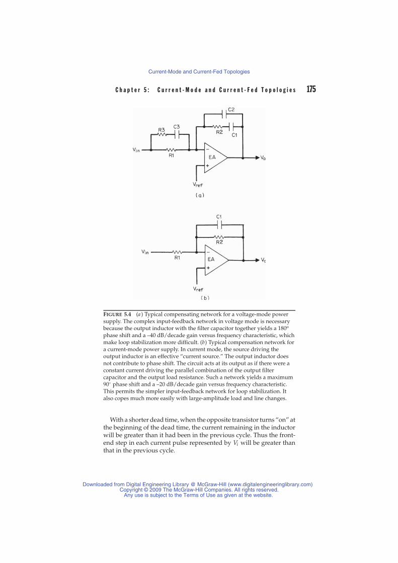
C h a p t e r 5 : C u r r e n t - M o d e a n d C u r r e n t - F e d T o p o l o g i e s 175
FIGURE 5.4 (a ) Typical compensating network for a voltage-mode powersupply. The complex input-feedback network in voltage mode is necessarybecause the output inductor with the filter capacitor together yields a 180o
phase shift and a –40 dB/decade gain versus frequency characteristic, whichmake loop stabilization more difficult. (b) Typical compensation network fora current-mode power supply. In current mode, the source driving theoutput inductor is an effective “current source.” The output inductor doesnot contribute to phase shift. The circuit acts at its output as if there were aconstant current driving the parallel combination of the output filtercapacitor and the output load resistance. Such a network yields a maximum90◦ phase shift and a –20 dB/decade gain versus frequency characteristic.This permits the simpler input-feedback network for loop stabilization. Italso copes much more easily with large-amplitude load and line changes.
With a shorter dead time, when the opposite transistor turns “on” atthe beginning of the dead time, the current remaining in the inductorwill be greater than it had been in the previous cycle. Thus the front-end step in each current pulse represented by Vi will be greater thanthat in the previous cycle.
Downloaded from Digital Engineering Library @ McGraw-Hill (www.digitalengineeringlibrary.com)Copyright © 2009 The McGraw-Hill Companies. All rights reserved.
Any use is subject to the Terms of Use as given at the website.
Current-Mode and Current-Fed Topologies
176 S w i t c h i n g P o w e r S u p p l y D e s i g n
This process continues for a number of switching cycles, until thestep part of the ramp-on-a-step current waveform builds up suffi-ciently to supply the increased demand for DC load current. As thiscurrent builds up, the DC output voltage gradually builds back up andVeao relaxes back down, returning the “on” time to its original value.The time to respond to a change in DC load current is thus seen tobe dependent on the size of the output inductor, since a smaller valuepermits more rapid current changes. The response time also dependson the bandwidth of the error amplifier.
5.5 Current-Mode Deficienciesand Limitations5.5.1 Constant Peak Current vs. Average
Output Current Ratio Problem1–4
Current mode controls the peak transistor currents (and hence thepeak output inductor/choke currents) constant at a level needed tosupply the required mean DC load current to give the mean DC outputvoltage dictated by the voltage error amplifier, as shown in Figure 5.3.
The DC load current is the average of the output inductor currentso that keeping the peak transistor current constant, and hence thepeak output inductor current constant, does not keep the averageinductor current and hence output current constant. Because of this,in the unmodified current-mode scheme described thus far, changes inthe DC input voltage will cause momentary changes in the DC outputvoltage. After a short delay the output voltage change will be correctedby the voltage error amplifier in the outer feedback loop, as this is theloop that ultimately sets output voltage.
After Pressman This is now referred to as the “peak to average cur-rent ratio” effect. The problem stems from the fact that maintaining the peakinductor current constant does not maintain the average output current con-stant, because duty cycle changes change the average value but not the peakvalue. This can become a problem for wide duty cycle changes, leading to sub-harmonic instability. It is corrected by ramp compensation (Section 5.5.3).∼K.B.
However, the inner loop, in keeping peak inductor current con-stant, does not supply the correct average inductor current and outputvoltage changes again. The effect is an oscillation that commences atevery change in input voltage and that may continue for some time.The mechanism can be better understood from an examination of theup- and down-slopes of the output inductor currents in Figure 5.5.3
Downloaded from Digital Engineering Library @ McGraw-Hill (www.digitalengineeringlibrary.com)Copyright © 2009 The McGraw-Hill Companies. All rights reserved.
Any use is subject to the Terms of Use as given at the website.
Current-Mode and Current-Fed Topologies
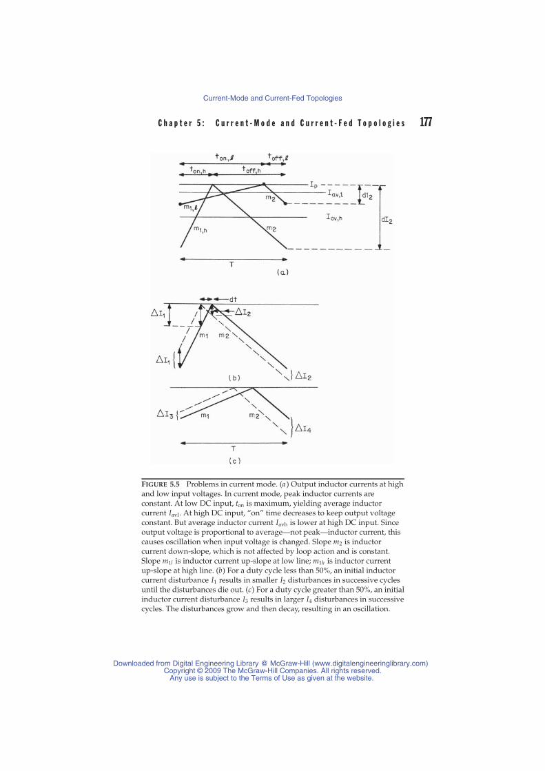
C h a p t e r 5 : C u r r e n t - M o d e a n d C u r r e n t - F e d T o p o l o g i e s 177
FIGURE 5.5 Problems in current mode. (a ) Output inductor currents at highand low input voltages. In current mode, peak inductor currents areconstant. At low DC input, ton is maximum, yielding average inductorcurrent Iavl. At high DC input, “on” time decreases to keep output voltageconstant. But average inductor current Iavh is lower at high DC input. Sinceoutput voltage is proportional to average—not peak—inductor current, thiscauses oscillation when input voltage is changed. Slope m2 is inductorcurrent down-slope, which is not affected by loop action and is constant.Slope m1l is inductor current up-slope at low line; m1h is inductor currentup-slope at high line. (b) For a duty cycle less than 50%, an initial inductorcurrent disturbance I1 results in smaller I2 disturbances in successive cyclesuntil the disturbances die out. (c) For a duty cycle greater than 50%, an initialinductor current disturbance I3 results in larger I4 disturbances in successivecycles. The disturbances grow and then decay, resulting in an oscillation.
Downloaded from Digital Engineering Library @ McGraw-Hill (www.digitalengineeringlibrary.com)Copyright © 2009 The McGraw-Hill Companies. All rights reserved.
Any use is subject to the Terms of Use as given at the website.
Current-Mode and Current-Fed Topologies
178 S w i t c h i n g P o w e r S u p p l y D e s i g n
Figure 5.5a shows the up- and down-slopes of the output inductorcurrent for two different DC input voltages in current mode. Slope m2is the down-slope = dI1/dt= Vo/Lo . It is seen to be constant for thetwo different DC input voltages. At the high input voltage, “on” timeis short at ton,h and at the lower DC input, “on” time is longer at ton,l .
The peak inductor currents are constant because the power tran-sistor peak currents are kept constant by the PWM comparator (seeFigure 5.3). The DC voltage input Veao to that comparator is constantsince the outer feedback loop is keeping Vo constant. The constantVeao then keeps Vi peaks constant, and hence transistor and outputinductor peak currents are constant.
In Figure 5.5a , in the steady state, the current change in the outputinductor during an “on” time is equal and opposite to that during an“off” time. If this were not so, there would be a DC voltage acrossthe inductor, and since it is assumed that the inductor has negligibleresistance, it cannot support DC voltage.
It can be seen in Figure 5.5a that the average inductor current atlow DC input is higher than it is at high DC input voltage. This canbe seen quantitatively as
Iav = Ip − dI2
2
= Ip −(m2toff
2
)
= Ip −[
m2(T − ton)2
]
= Ip −(
m2T2
)+
(m2ton
2
)(5.1)
Since the voltage feedback loop keeps the product of Vdcton constant,at lower DC input voltage when the “on” time is higher, the averageoutput inductor current Iav is higher, as can be seen from Eq. 5.1 andFigure 5.5a .
Further, since the DC output voltage is proportional to the averageand not the peak inductor current, as DC input goes down, DC outputvoltage will go up. DC output voltage will then be corrected by theouter feedback loop and a seesaw action or oscillation will occur.
This phenomenon does not occur in voltage-mode control, inwhich only DC output voltage is controlled. Also, since DC outputvoltage is proportional to average and not peak inductor current,keeping output voltage constant maintains average inductor currentconstant.
Downloaded from Digital Engineering Library @ McGraw-Hill (www.digitalengineeringlibrary.com)Copyright © 2009 The McGraw-Hill Companies. All rights reserved.
Any use is subject to the Terms of Use as given at the website.
Current-Mode and Current-Fed Topologies

C h a p t e r 5 : C u r r e n t - M o d e a n d C u r r e n t - F e d T o p o l o g i e s 179
5.5.2 Response to an Output InductorCurrent Disturbance
A second problem that gives rise to oscillation in current mode isshown in Figure 5.5b and 5.5c. In Figure 5.5b, it is seen that at a fixedDC input voltage, if for some reason there is an initial current distur-bance �I1, after a first down-slope the current will be displaced by anamount �I2.
Further, if the duty cycle is less than 50% (m2 < m1), as in Figure 5.5b,the output disturbance �I2 will be less than the input disturbance �I1,and after a few cycles, the disturbance will die out. If the duty cycle isgreater than 50% (m2 > m1) as in Figure 5.5c, the output disturbance�I4 after one cycle is greater than the input disturbance �I3. This canbe seen quantitatively from Figure 5.5b as follows. For a small currentdisplacement �I1, the current reaches the original peak value earlierin time by an amount dt where dt = �I1/m1.
On the inductor down-slope, at the end of the “on” time, the currentis lower than its original value by an amount �I2 where
�I2 = m2dt = �I1m2
m1(5.2)
Now with m2 greater than m1, the disturbances will continue to growbut eventually decay, giving rise to an oscillation.
5.5.3 Slope Compensation to CorrectProblems in Current Mode1–4
Both current-mode problems mentioned above can be corrected asshown in Figure 5.6, in which the original, unmodified output of theerror amplifier is shown as the horizontal voltage level OP. The “slopecompensation” scheme for correcting the preceding problems consistsof adding a negative voltage slope of magnitude m to the output of theerror amplifier. By proper selection of m in a manner discussed below,the output inductor average DC current can be made independent ofthe power transistor “on” time. This corrects the problems indicatedby both Eqs. 5.1 and 5.2.
In Figure 5.6, the up-slope m1 and down-slope m2 of output inductorcurrent are shown. Recall that in current mode, the power transistor“on” time starts at every clock pulse and ends at the instant the out-put of the PWM comparator reaches equality with the output of thevoltage error-amplifier as shown in Figure 5.3. In slope compensation,a negative voltage slope of magnitude m = dVea/dt starting at clocktime is added to the error-amplifier output. The magnitude of m iscalculated thus: In Figure 5.6, the error-amplifier output at any time
Downloaded from Digital Engineering Library @ McGraw-Hill (www.digitalengineeringlibrary.com)Copyright © 2009 The McGraw-Hill Companies. All rights reserved.
Any use is subject to the Terms of Use as given at the website.
Current-Mode and Current-Fed Topologies
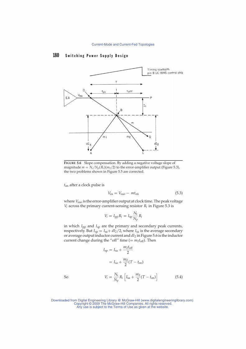
180 S w i t c h i n g P o w e r S u p p l y D e s i g n
FIGURE 5.6 Slope compensation. By adding a negative voltage slope ofmagnitude m = Ns/Np(Ri )(m2/2) to the error-amplifier output (Figure 5.3),the two problems shown in Figure 5.5 are corrected.
ton after a clock pulse is
Vea = Veao − mton (5.3)
where Veao is the error-amplifier output at clock time. The peak voltageVi across the primary current-sensing resistor Ri in Figure 5.3 is
Vi = Ipp Ri = IspNs
NpRi
in which Ipp and Isp are the primary and secondary peak currents,respectively. But Isp = Isa+ dI2/2, where Isa is the average secondaryor average output inductor current and dI2 in Figure 5.6 is the inductorcurrent change during the “off” time (= m2toff). Then
Isp = Isa + m2toff
2
= Isa + m2
2(T − ton)
So Vi = Ns
NpRi
[Isa + m2
2(T − ton)
](5.4)
Downloaded from Digital Engineering Library @ McGraw-Hill (www.digitalengineeringlibrary.com)Copyright © 2009 The McGraw-Hill Companies. All rights reserved.
Any use is subject to the Terms of Use as given at the website.
Current-Mode and Current-Fed Topologies
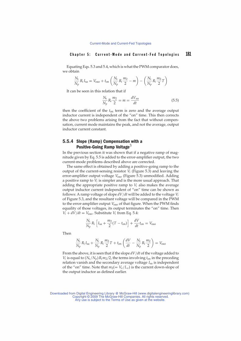
C h a p t e r 5 : C u r r e n t - M o d e a n d C u r r e n t - F e d T o p o l o g i e s 181
Equating Eqs. 5.3 and 5.4, which is what the PWM comparator does,we obtain
Ns
NpRi Isa = Veao + ton
(Ns
NpRi
m2
2− m
)−
(Ns
NpRi
m2
2T
)
It can be seen in this relation that if
Ns
NpRi
m2
2= m = dVea
dt(5.5)
then the coefficient of the ton term is zero and the average outputinductor current is independent of the “on” time. This then correctsthe above two problems arising from the fact that without compen-sation, current mode maintains the peak, and not the average, outputinductor current constant.
5.5.4 Slope (Ramp) Compensation with aPositive-Going Ramp Voltage3
In the previous section it was shown that if a negative ramp of mag-nitude given by Eq. 5.5 is added to the error-amplifier output, the twocurrent-mode problems described above are corrected.
The same effect is obtained by adding a positive-going ramp to theoutput of the current-sensing resistor Vi (Figure 5.3) and leaving theerror-amplifier output voltage Veao (Figure 5.3) unmodified. Addinga positive ramp to Vi is simpler and is the more usual approach. Thatadding the appropriate positive ramp to Vi also makes the averageoutput inductor current independent of “on” time can be shown asfollows: A ramp voltage of slope dV/dt will be added to the voltage Viof Figure 5.3, and the resultant voltage will be compared in the PWMto the error-amplifier output Veao of that figure. When the PWM findsequality of those voltages, its output terminates the “on” time. ThenVi + dV/dt = Veao. Substitute Vi from Eq. 5.4:
Ns
NpRi
[Isa + m2
2(T − ton)
]+ dV
dtton = Veao
Then
Ns
NpRi Isa + Ns
NpRi
m2
2T + ton
(dVdt
− Ns
NpRi
m2
2
)= Veao
From the above, it is seen that if the slope dV/dt of the voltage added toVi is equal to (Ns/Np)Ri m2/2, the terms involving ton in the precedingrelation vanish and the secondary average voltage Isa is independentof the “on” time. Note that m2(= Vo/Lo ) is the current down-slope ofthe output inductor as defined earlier.
Downloaded from Digital Engineering Library @ McGraw-Hill (www.digitalengineeringlibrary.com)Copyright © 2009 The McGraw-Hill Companies. All rights reserved.
Any use is subject to the Terms of Use as given at the website.
Current-Mode and Current-Fed Topologies
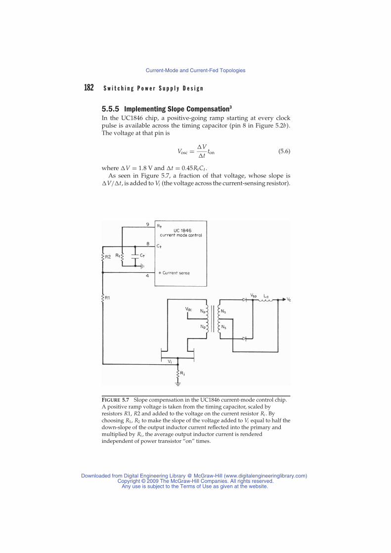
182 S w i t c h i n g P o w e r S u p p l y D e s i g n
5.5.5 Implementing Slope Compensation3
In the UC1846 chip, a positive-going ramp starting at every clockpulse is available across the timing capacitor (pin 8 in Figure 5.2b).The voltage at that pin is
Vosc = �V�t
ton (5.6)
where �V = 1.8 V and �t = 0.45RtCt.
As seen in Figure 5.7, a fraction of that voltage, whose slope is�V/�t, is added to Vi (the voltage across the current-sensing resistor).
FIGURE 5.7 Slope compensation in the UC1846 current-mode control chip.A positive ramp voltage is taken from the timing capacitor, scaled byresistors R1, R2 and added to the voltage on the current resistor Ri . Bychoosing R1, R2 to make the slope of the voltage added to Vi equal to half thedown-slope of the output inductor current reflected into the primary andmultiplied by Ri , the average output inductor current is renderedindependent of power transistor “on” times.
Downloaded from Digital Engineering Library @ McGraw-Hill (www.digitalengineeringlibrary.com)Copyright © 2009 The McGraw-Hill Companies. All rights reserved.
Any use is subject to the Terms of Use as given at the website.
Current-Mode and Current-Fed Topologies

C h a p t e r 5 : C u r r e n t - M o d e a n d C u r r e n t - F e d T o p o l o g i e s 183
That slope is set to (Ns/Np)Ri (m2/2) by resistors R1, R2. Thus in Fig-ure 5.7, since Ri is much less than R1, the voltage delivered to thecurrent-sensing terminal (pin 4) is
Vi + R1R1 + R2
Vosc = Vi + R1R1 + R2
�V�t
ton (5.7)
and setting the slope of that added voltage equal to (Ns/Np)Ri m2/2,we obtain
R1R1 + R2
= (Ns/Np)(Ri )(m2/2)�V/�t
(5.8)
in which �V/�t = 1.8/(0.45RtCt).Since R1+ R2 drains current from the timing capacitor, they change
operating frequency. Then either R1 + R2 is made large enough sothat the frequency change is small, or a buffer amplifier is interposedbetween pin 8 and the resistors. Usually R1 is preselected and R2 iscalculated from Eq. 5.8.
After Pressman With large values of inductance Lo or at higher frequen-cies, the slope on the current waveform (Figure 5.5) as it approaches the pointof transition to the “off” state can approach zero. Hence any small noise spikecan cause early or late switching resulting in jitter and noise in the output.In effect, the gain of the fast current control loop becomes very high. Closeattention to layout and using a non-inductive current-sensing resistor for Rior a DCCT may help. But in many cases the solution requires a reduction ininductance resulting in an increase in high frequency ripple current. ∼K.B.
5.6 Comparing the Properties ofVoltage-Fed and Current-Fed Topologies5.6.1 Introduction and DefinitionsAll topologies discussed thus far have been of the voltage-fed type.Voltage-fed implies that the source impedance of whatever drives thetopology is low and hence there is no way of limiting the currentdrawn from it during unusual conditions at power switch turn “on”or turn “off,” or under various fault conditions in the topology.
There are various ways of implementing “current limiting” withadditional circuitry, which senses an over-current condition and takessome kind of corrective action such as narrowing the controller’sswitching pulse width or stopping it completely. But all such schemesare not instantaneous; they involve a delay over a number of switch-ing cycles during which there can be excessive dissipation in eitherthe power transistors or output rectifiers and dangerous voltage or
Downloaded from Digital Engineering Library @ McGraw-Hill (www.digitalengineeringlibrary.com)Copyright © 2009 The McGraw-Hill Companies. All rights reserved.
Any use is subject to the Terms of Use as given at the website.
Current-Mode and Current-Fed Topologies

184 S w i t c h i n g P o w e r S u p p l y D e s i g n
current spiking. Thus such over-current sensing schemes are of nohelp in the case of high transient currents at the instant of the powerswitch turn “on” and turn “off.”
The low-source impedance in voltage-fed topologies is that of thefilter capacitor in offline converters or of the battery in battery-powered converters. In compound schemes that use a buck regulatorto preregulate the rectified DC voltage of the AC line rectifier, it is thevery low-output impedance of the buck regulator itself.
In current-fed topologies, the high instantaneous impedance of aninductor is interposed between the power source and the topologyitself. This provides a number of significant advantages, especiallyin high power supplies (> 1000 W), high output voltage supplies(> 200 V), and multi-output supplies where close tracking betweenslaves and a master output voltage is required.
Advantages of the current-fed technique can be appreciated by ex-amining the usual shortcomings of high-power, high-output-voltage,and multi-output voltage-fed topologies.
5.6.2 Deficiencies of Voltage-Fed, Pulse-Width-Modulated Full-Wave Bridge9
Figure 5.8 shows a conventional voltage-fed full bridge—the usualchoice for a switching supply at 1000-W output. At higher outputpowers, high output voltages, or multiple output voltages, it has thefollowing significant shortcomings.
FIGURE 5.8 A conventional voltage-fed full bridge, often used for higher out-put powers typically 1000 W or more. The low-source impedance of the filtercapacitor C f and the need for the output inductor Lo are significant drawbacksfor output powers over 1000 W and output voltages over a few hundredvolts. Further, in a multi-output power supply, the requirement for an outputinductor at each output makes the topology expensive in cost and space.
Downloaded from Digital Engineering Library @ McGraw-Hill (www.digitalengineeringlibrary.com)Copyright © 2009 The McGraw-Hill Companies. All rights reserved.
Any use is subject to the Terms of Use as given at the website.
Current-Mode and Current-Fed Topologies

C h a p t e r 5 : C u r r e n t - M o d e a n d C u r r e n t - F e d T o p o l o g i e s 185
5.6.2.1 Output Inductor Problems in Voltage-Fed,Pulse-Width-Modulated Full-Wave Bridge
For high-output voltages, the size and cost of the output inductor Lo(or inductors in a multi-output supply) becomes prohibitive as canbe seen from the following. The inductor is selected to prevent goinginto the discontinuous mode or running dry at the specified minimumDC load current (Sections 1.3.6 and 2.2.14.1). For a minimum DC loadcurrent of one-tenth the nominal Ion, Eq. 2.20 gives the magnitude ofthe inductor as Lo = 0.5Vo T/Ion.
Now consider a 2000-W supply at Vo = 200 V, Io(nominal) = 10 A,and a minimum DC output current of 1 A. To minimize the size of theoutput inductor, T should be minimized, and a switching frequencyof 50 kHz might be considered. At 50 kHz, for Vo = 200 V, Ion = 10 A,Eq. 2.20 yields Lo of 200 μH.
The inductor must carry the nominal current of 10 A without satu-rating. Inductors capable of carrying large DC bias currents withoutsaturating are discussed in a later chapter and are made either withgapped ferrite or powdered iron toroidal cores. A 200-μH 10-A induc-tor using a powdered iron toroid would have a diameter about 2.5 inand a height about 1.0 in.
Although this is not a prohibitive size for a single-output 2-kWsupply, a supply with many outputs, higher output voltage, or higheroutput power, the size and cost of many large inductors would be aserious drawback. For high-output voltages (> 1000 V), even at low-output currents, the output inductor is far more troublesome becauseof the large number of turns required to support the high voltageacross the inductor. This high voltage—especially during the deadtime when cathodes of D5, D6 of Figure 5.8 are both “low”—canproduce corona and arcing.
A further problem with a topology requiring output inductors, asshown in Figure 5.8, is the poor cross regulation or change in outputvoltage of a slave when current changes in the master (Section 2.2.2).The output inductors in both the master and slave must be largeenough to prevent discontinuous mode operation and large-outputvoltage changes at minimum load currents.
The current-fed topology (Figure 5.10) discussed below avoidsmany of the above problems, as it does not require multiple out-put inductors. It uses a single input inductor L1 in place of theindividual output inductors, and is positioned before the high fre-quency switching bridge circuit and after line rectification and stor-age capacitors. Thus DC output voltages are the peak rather thanthe average of the transformer secondary voltages. Voltage regula-tion is achieved by pulse-width modulation of the bridge, or as inFigure 5.10, by a buck regulator transistor switch Q5 ahead of the L1inductor.
Downloaded from Digital Engineering Library @ McGraw-Hill (www.digitalengineeringlibrary.com)Copyright © 2009 The McGraw-Hill Companies. All rights reserved.
Any use is subject to the Terms of Use as given at the website.
Current-Mode and Current-Fed Topologies

186 S w i t c h i n g P o w e r S u p p l y D e s i g n
5.6.2.2 Turn “On” Transient Problems in Voltage-Fed,Pulse-Width-Modulated Full-Wave Bridge9
In Figure 5.8, diagonally opposite transistors are simultaneously “on”during alternate half cycles. The maximum “on” time of each pair isdesigned to be less than 80% of a half period. This ensures a 0.2T/2dead time between the turn “off” of one transistor pair and the turn“on” of the other. This dead time is essential, for if the “on” time ofalternate pairs overlapped by even a fraction of a microsecond, therewould be a dead short circuit across the filter capacitor, and withnothing to limit current flow, the transistors would fail immediately.
During the dead time, all four transistors are “off,” the anodes ofoutput rectifiers D5, D6 are at zero volts, and the voltage at the inputend of filter inductor Lo has swung down to keep the current constant.The input end of Lo is clamped at one diode drop below ground byD5, D6, which act as free-wheeling diodes. The current that had beenflowing in Lo before the dead time (roughly equal to the DC outputcurrent) continues to flow in the same direction. It flows out throughthe ground terminal into the secondary center tap, where it dividesequally with half flowing through each of D5 and D6 and back intothe input end of Lo .
At the start of the next half cycle when, say, Q1, Q2 turn “on,” theno-dot end of the T1 primary is high and the no-dot end of the T1secondary (anode of D6) attempts to go high. But the cathode of D6is looking into the cathode of D5, which is still conducting half theDC output current. Until D6 supplies a current equal to and cancelingthe D5 forward current, it is looking into the low impedance of aconducting diode (∼10 �).
This low secondary impedance reflects as a low impedance acrossthe primary. But this low impedance is in series with the transformer’sleakage inductance, which limits the primary current during the timerequired to cancel the D5 free-wheeling current. Because of the high-impedance current-limiting effect of the leakage inductance, transis-tors Q1 and Q2 remain in saturation until the D5 free-wheeling currentis canceled.
When the D5 current is canceled, it still has a low impedancebecause of its reverse-recovery time, which may range from 35 ns(ultra-fast-recovery type) to 200 ns (fast-recovery type). For a reverse-recovery time of tr , supply voltage of Vcc, and transformer primaryleakage inductance of Ll , the primary current overshoots to Vcctr/Ll .This overshoot current can pull the transistors out of saturation andeither damage or destroy them.
Finally, when the output rectifier recovers abruptly, there is adamped oscillatory ring at its cathode. The first positive half cycleof this ring can more than double the reverse voltage stress on thediode and possibly destroy it. Even in lower power supplies, it is often
Downloaded from Digital Engineering Library @ McGraw-Hill (www.digitalengineeringlibrary.com)Copyright © 2009 The McGraw-Hill Companies. All rights reserved.
Any use is subject to the Terms of Use as given at the website.
Current-Mode and Current-Fed Topologies
C h a p t e r 5 : C u r r e n t - M o d e a n d C u r r e n t - F e d T o p o l o g i e s 187
necessary to put series RC snubbers across the rectifiers to damp theoscillation. The penalty paid for this is, of course, dissipation in theresistors.
5.6.2.3 Turn “Off” Transient Problems in Voltage-Fed,Pulse-Width-Modulated Full-Wave Bridge9
In Figure 5.8, there is a spike of high power dissipation at turn “off”as a result of the instantaneous overlap of falling current and risingvoltage across the “off”-turning transistors.
Consider that Q3 and Q4 are “on” and have received turn “off”signals at their bases. As Q3, Q4 commence turning “off,” currentstored in the leakage and magnetizing inductance of T1 force a polar-ity reversal across the primary. The bottom end of T1 primary goesimmediately positive and is clamped via D1 to the positive rail at thetop of C f . The top end of T1 primary goes immediately negative andis clamped via D2 to the negative rail at the bottom end of C f . Nowvoltages across Q3 and Q4 are clamped at Vcc so long as diodes D1,D2 conduct. There are no leakage inductance voltage spikes acrossQ3, Q4 as in push-pull or single-ended forward converter topologies.Energy stored in the leakage inductance is returned without dissipa-tion to the input capacitor C f .
However, while the voltage across Q3, Q4 is held at Vcc, the currentin these two transistors falls linearly to zero in a time t f determinedby their reverse base drives. This overlap of a fixed-voltage Vcc and acurrent falling linearly from a value Ip results in dissipation averagedover a full period T of
PD = VccIp
2t f
T(5.9)
It is instructive to calculate this dissipation for, say, a 2-kW supplyoperating at 50 kHz from a nominal Vcc of 336 V (typical Vcc for anoffline inverter operating from a 120-V AC line in the voltage-doublingmode as in Section 3.1.1). Assume a minimum Vcc of 0.9 (336 V) or302 V. Then from Eq. 3.7, the peak current is
Ip = 1.56Po
Vdc= 1.56
2000302
= 10.3 A
A bipolar transistor at this current has a fall time of perhaps 0.3 μs.Since peak currents are independent of DC input voltage, calcu-late overlap dissipation from Eq. 5.9 at a high line of 1.1 × 336 =370 V. For the dissipation in either Q3 or Q4, Eq. 5.9 gives PD =Vcc( Ip/2)(t f /T) = 370(10.3/2)(0.3/20) = 28.5 W, and for the four tran-sistors in the bridge, total overlap losses would be 114 W.
Downloaded from Digital Engineering Library @ McGraw-Hill (www.digitalengineeringlibrary.com)Copyright © 2009 The McGraw-Hill Companies. All rights reserved.
Any use is subject to the Terms of Use as given at the website.
Current-Mode and Current-Fed Topologies

188 S w i t c h i n g P o w e r S u p p l y D e s i g n
It is of interest to calculate the dissipation per transistor during the“on” time. This is Vce(sat) Ic Ton/T and for a typical Vce(sat) of 1.0 V andan “on” duty cycle of 0.4 is only 1 × 10.3 × 0.4 or 4.1 W.
Even though the 28.5 W of overlap dissipation per transistor canbe reduced with four load- and line-shaping “snubbers” (to be dis-cussed in a later chapter), these snubbers reduce transistor losses onlyby diverting them to the snubber resistors with no improvement inefficiency. It will be shown that in the current-fed topology, only twosnubbers will be required, reducing transistor overlap dissipation to anegligible value. The price paid for this is the dissipation in each of thetwo snubber resistors of somewhat more than that in the voltage-fedfull bridge.
5.6.2.4 Flux-Imbalance Problem in Voltage-Fed,Pulse-Width-Modulated Full-Wave Bridge
Flux imbalance, or operation not centered about the origin of the trans-former’s BH loop, was discussed in Section 2.2.5 in connection withthe push-pull and in Section 3.2.4 for the half bridge. It arises becauseof unequal volt-second products applied to the transformer primaryon alternate half cycles. As the core drifts farther and farther off cen-ter on the BH loop, it can move into saturation where it is unable tosustain the supply voltage and destroy the transistor.
Flux imbalance can also arise in the conventional full-wave bridgebecause of a volt-second imbalance on alternate half cycles. This cancome about with bipolar transistors because of unequal storage timeson alternate half cycles or with MOSEFT transistors because of un-equal MOSEFT “on”-voltage drops. The solution for the full-wavebridge is to place a DC blocking capacitor in series with the primary.This prevents a DC current bias in the primary and forces operation tobe centered about the BH loop origin. The size of such a DC blockingcapacitor is calculated as in Section 3.2.4 for the half bridge.
The current-fed circuits, discussed below, do not require DC block-ing capacitors, providing another advantage over voltage-fed circuits.This is still an advantage despite the relatively small size and cost ofsuch blocking capacitors.
5.6.3 Buck Voltage-Fed Full-Wave BridgeTopology—Basic Operation
This topology is shown in Figure 5.9. It avoids many of the deficienciesof the voltage-fed pulse-width-modulated full-wave bridge in high-voltage, high-power, multi-output supplies.
Consider first how it works. There is a buck regulator preceding asquare-wave inverter, which has only capacitors after the secondary
Downloaded from Digital Engineering Library @ McGraw-Hill (www.digitalengineeringlibrary.com)Copyright © 2009 The McGraw-Hill Companies. All rights reserved.
Any use is subject to the Terms of Use as given at the website.
Current-Mode and Current-Fed Topologies
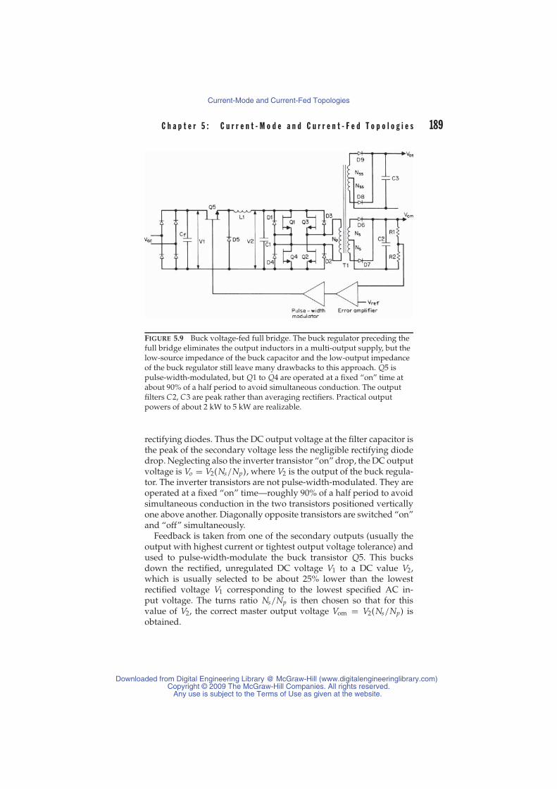
C h a p t e r 5 : C u r r e n t - M o d e a n d C u r r e n t - F e d T o p o l o g i e s 189
FIGURE 5.9 Buck voltage-fed full bridge. The buck regulator preceding thefull bridge eliminates the output inductors in a multi-output supply, but thelow-source impedance of the buck capacitor and the low-output impedanceof the buck regulator still leave many drawbacks to this approach. Q5 ispulse-width-modulated, but Q1 to Q4 are operated at a fixed “on” time atabout 90% of a half period to avoid simultaneous conduction. The outputfilters C2, C3 are peak rather than averaging rectifiers. Practical outputpowers of about 2 kW to 5 kW are realizable.
rectifying diodes. Thus the DC output voltage at the filter capacitor isthe peak of the secondary voltage less the negligible rectifying diodedrop. Neglecting also the inverter transistor “on” drop, the DC outputvoltage is Vo = V2(Ns/Np), where V2 is the output of the buck regula-tor. The inverter transistors are not pulse-width-modulated. They areoperated at a fixed “on” time—roughly 90% of a half period to avoidsimultaneous conduction in the two transistors positioned verticallyone above another. Diagonally opposite transistors are switched “on”and “off” simultaneously.
Feedback is taken from one of the secondary outputs (usually theoutput with highest current or tightest output voltage tolerance) andused to pulse-width-modulate the buck transistor Q5. This bucksdown the rectified, unregulated DC voltage V1 to a DC value V2,which is usually selected to be about 25% lower than the lowestrectified voltage V1 corresponding to the lowest specified AC in-put voltage. The turns ratio Ns/Np is then chosen so that for thisvalue of V2, the correct master output voltage Vom = V2(Ns/Np) isobtained.
Downloaded from Digital Engineering Library @ McGraw-Hill (www.digitalengineeringlibrary.com)Copyright © 2009 The McGraw-Hill Companies. All rights reserved.
Any use is subject to the Terms of Use as given at the website.
Current-Mode and Current-Fed Topologies

190 S w i t c h i n g P o w e r S u p p l y D e s i g n
The feedback loop, in keeping Vom constant against line and loadchanges, then keeps V2 constant (neglecting relatively constant recti-fier diode drops) at V2 = Vo (Np/Ns). Additional secondaries, rectifierdiodes, and peak-rectifying filter capacitors can be added for slaveoutputs.
Alternatively, feedback can be taken from C1 to keep V2 constant.From V2 to the outputs, the circuit is open-loop. But all output voltagesare still quite insensitive to line and load changes because they changeonly slightly with forward drops in diode rectifiers and “on” drops ofthe transistors, which change only slightly with output currents. Thusthe output voltages are all largely proportional to V2.
Taking feedback from V2 results in somewhat less constant out-put voltage, but avoids the problem of transmitting a pulse-width-modulated control voltage pulse across the boundary from output toinput common. If an error amplifier is located on output common witha pulse-width modulator on input common, it avoids the problem oftransmitting the amplified DC error voltage across the output-inputboundary. Such a scheme usually involves the use of an optocoupler,which has wide tolerances in gain and is not too reliable a device.
5.6.4 Buck Voltage-Fed Full-Wave BridgeAdvantages
5.6.4.1 Elimination of Output InductorsThe first obvious advantage of the topology for a multi-output supplyis that it replaces many output inductors with a single input inductorwith consequent savings in cost and space.
Since there are no output inductors in either the master or slaves,there is no problem with large output voltage changes that result fromoperating the inductors in discontinuous mode (Sections 1.3.6 and2.2.4). Slave output voltages track the master over a large range ofoutput currents, within about ±2%, rather than the ±6 to ±8% withoutput inductors in continuous mode, or substantially more in dis-continuous mode.
After Pressman Providing the outputs share a common return, this prob-lem can also be solved in the multiple output inductor case by using thecoupled inductor approach. Here a single inductor has a winding for eachoutput wound on a single core. The transformer type coupling between thewindings also eliminates many of the problems shown above.1 ∼K.B.
The input inductor is designed to operate in continuous mode atany current above the minimum. Since it is unlikely that all outputsare at minimum current simultaneously, this indicates a higher totalminimum current and a smaller input inductor (Section 1.3.6).
Downloaded from Digital Engineering Library @ McGraw-Hill (www.digitalengineeringlibrary.com)Copyright © 2009 The McGraw-Hill Companies. All rights reserved.
Any use is subject to the Terms of Use as given at the website.
Current-Mode and Current-Fed Topologies
C h a p t e r 5 : C u r r e n t - M o d e a n d C u r r e n t - F e d T o p o l o g i e s 191
Further, even if the input inductor goes discontinuous, the masteroutput voltage will remain substantially constant, but with somewhatmore output ripple and somewhat poorer load regulation. The feed-back loop will keep the main output voltage constant even in dis-continuous mode through large decreases in “on” time of the bucktransistor (Figure 1.6a ).
Further, since the slave outputs are clamped to the main outputin the ratio of their respective turns ratios, slaves will also remainconstant against large line and load changes.
Elimination of output inductors, with the many turns required tosustain high AC voltages for high voltage DC outputs, makes 2000-to 3000-V outputs easily feasible. Higher output voltages—15,000 to30,000 V—at relatively low-output currents as for cathode-ray tubes,or high-voltage high-current outputs as for traveling-wave tubes, areeasily obtained by conventional diode-capacitor voltage multipliersafter the secondaries.8
5.6.4.2 Elimination of Bridge Transistor Turn “On” TransientsWith respect to the full-wave pulse-width-modulated bridge ofFigure 5.8, Section 5.6.2.2 discussed turn “on” transient currentstresses in the bridge transistors (Q1 to Q4), and excessive voltagestress in the rectifying diodes (D5, D6).
It was pointed out in Section 5.6.2.2 that these stresses arose becausethe rectifier diodes were also acting as free-wheeling diodes. At theinstant of turn “on” of one diagonally opposite pair (say Q1, Q2),D6 was still conducting as a free-wheeling diode. Until the forwardcurrent in D6 was canceled, the impedance seen by Q1, Q2 was theleakage inductance of T1 in series with the low forward impedanceof D6 reflected into the primary.
Subsequently, when Q1, Q2 forced a current into the primary suffi-cient to cancel the D6 forward current, there was still a low impedancereflected into the primary because of reverse recovery time in D6. Thiscaused a large primary current overshoot that overstressed Q1, Q2.At the end of the recovery time, when the large secondary currentovershoot terminated, it caused an oscillation and excessive voltagestress on D6.
This current overstress on the bridge transistors and voltage over-stress on the output rectifiers does not occur with the buck voltage-fedtopology of Figure 5.9. The inverter transistors are operated with adead time (∼ 0.1T/2) between the turn “off” of one pair of transistorsand the turn “on” of the other pair.
During this dead time when none of the bridge transistors are “on,”no current flows in the output rectifiers and output load current is
Downloaded from Digital Engineering Library @ McGraw-Hill (www.digitalengineeringlibrary.com)Copyright © 2009 The McGraw-Hill Companies. All rights reserved.
Any use is subject to the Terms of Use as given at the website.
Current-Mode and Current-Fed Topologies

192 S w i t c h i n g P o w e r S u p p l y D e s i g n
supplied from the filter capacitors alone. Thus at the start of the nexthalf period, the “on”-turning rectifier diode is not loaded down witha conducting free-wheeling diode as in Figure 5.8. The opposite diodehas long since ceased conducting; thus there is no current overstress inthe bridge transistors, no recovery time problem in the rectifier diodes,and hence no overvoltage stress in them.
5.6.4.3 Decrease of Bridge Transistor Turn “Off” DissipationIn Section 5.6.2.3, it was calculated that for a 2000-W supply operatingfrom a nominal input of 120-V AC in the input voltage-doubling mode,the bridge dissipation is 28.5 W at maximum AC input for each ofthe four transistors in the voltage-fed, pulse-width-modulated bridgecircuit of Figure 5.8.
In the buck voltage-fed, full-wave bridge (Figure 5.9), this dissi-pation is somewhat less. This is so because, even at maximum ACinput, the “off”-turning bridge transistors are subjected to bucked-down voltage V2 (Figure 5.9) of about 0.75 times the minimum recti-fied voltage as discussed in Section 5.6.3. For the minimum rectifiedDC of 302 V (Section 5.6.2.3), this is 0.75 × 302 or 227 V. This com-pares favorably to the 370 V DC at maximum AC input as calculatedin Section 5.6.2.3.
The peak current from the bucked-down 227 V will not differmuch from the 10.3 A calculated in Section 5.6.2.3. Thus assume atotal efficiency of 80%, as for the circuit of Figure 5.8. Assume thathalf the losses are in the bridge and half in the buck regulator ofFigure 5.9. Then for a bridge efficiency of 90%, its input power is2000/0.9 or 2222 W. With a preregulated input, the bridge transis-tors can operate at 90% duty cycle without concern about simul-taneous conduction. Input power is then 0.9IpVdc = 2222 W. ForVdc of 227 V as above, this yields Ip of 10.8 A. Calculating bridgetransistor dissipation as in Section 5.6.2.3 for a current fall time t fof 0.3 μs out of a period T of 20 μs, dissipation per transistor is(Ip/2)(Vdc)(t f /T) = (10.8/2)227 × 0.3/20 = 18.4 W. This is 74 W forthe entire bridge as compared to 114 W for the circuit of Figure 5.8 ascalculated in Section 5.6.2.3.
5.6.4.4 Flux-Imbalance Problem in Bridge TransformerThis problem is still the same as in the topology of Figure 5.8. Avolt-second unbalance can occur because of unequal storage timesfor bipolar bridge transistors or because of unequal “on” voltagesfor MOSFET transistors. The solution for both the Figure 5.8 andFigure 5.9 topologies is to insert a DC blocking capacitor in serieswith the transformer primary.
Downloaded from Digital Engineering Library @ McGraw-Hill (www.digitalengineeringlibrary.com)Copyright © 2009 The McGraw-Hill Companies. All rights reserved.
Any use is subject to the Terms of Use as given at the website.
Current-Mode and Current-Fed Topologies

C h a p t e r 5 : C u r r e n t - M o d e a n d C u r r e n t - F e d T o p o l o g i e s 193
5.6.5 Drawbacks in Buck Voltage-FedFull-Wave Bridge9,10
Despite the advantages over the pulse-width-modulated full-waveinverter bridge, the buck voltage-fed full-wave bridge has a numberof significant drawbacks.
First, there are the added cost, volume, and power dissipation of thebuck transistor Q5 (Figure 5.9) and the cost and volume of the buck LCfilter (L1, C1). The added cost and volume of these elements is partlycompensated by the saving of an inductor at each output. The addeddissipations of the buck regulator Q5 and the free-wheeling diode D5are most often a small percentage of the total losses for a ≥ 2000-Wpower supply.
Second, there are turn “on” and turn “off” transient losses in thebuck transistor, which can be greater than its DC conduction losses.These can be reduced in the transistor by diverting them to passiveelements in snubbers. But the losses, cost, and required space of thesnubbers is still a drawback. Turn “on”–turn “off” snubbers will bediscussed in the later section on the buck current-fed full-wave bridge.
The turn “off” transient losses in the bridge transistors, althoughless than for the pulse-width-modulated bridge of Figure 5.8, stillremain significant. (See the discussion in Section 5.6.4.3.)
Finally, under conditions of unusually long storage time at hightemperature and low load or low line, at the turn “on” of one tran-sistor pair, the opposite pair may still be “on.” With the low-sourceimpedance of the buck filter capacitor and the momentary short cir-cuit across the supply bus, this will cause immediate failure of at leastone, and possibly all, of the bridge transistors.
5.6.6 Buck Current-Fed Full-Wave BridgeTopology—Basic Operation9,10
This topology is shown in Figure 5.10.6 It has no output inductors andis exactly like the buck voltage-fed full-wave bridge of Figure 5.9 withthe exception that there is no buck filter capacitor C1. Instead, thereis a virtual capacitor C1V, which is the sum of all the secondary filtercapacitors reflected by the squares of their respective turns ratios intothe T1 primary. The filtering by this virtual capacitor C1V is exactlythe same as that of a real capacitor of equal magnitude.
Thus, by replacing all the output inductors of the pulse-width-modulated full-wave bridge of Figure 5.8 with a single primary sideinductor as in Figure 5.9, all the advantages described in Section 5.6.2.1for the Figure 5.9 circuit are also obtained for the circuit of Figure 5.10.
Bridge transistors Q1 to Q4 are not pulse-width-modulated, as theywere in Figure 5.8. In this topology, diagonally opposite transistors are
Downloaded from Digital Engineering Library @ McGraw-Hill (www.digitalengineeringlibrary.com)Copyright © 2009 The McGraw-Hill Companies. All rights reserved.
Any use is subject to the Terms of Use as given at the website.
Current-Mode and Current-Fed Topologies
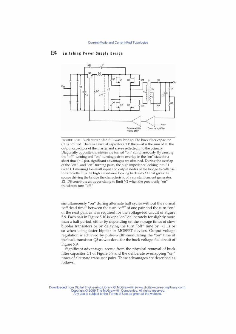
194 S w i t c h i n g P o w e r S u p p l y D e s i g n
FIGURE 5.10 Buck current-fed full-wave bridge. The buck filter capacitorC1 is omitted. There is a virtual capacitor C1V there—it is the sum of all theoutput capacitors of the master and slaves reflected into the primary.Diagonally opposite transistors are turned “on” simultaneously. By causingthe “off”-turning and “on”-turning pair to overlap in the “on” state for ashort time (∼ 1 μs), significant advantages are obtained. During the overlapof the “off”- and “on”-turning pairs, the high impedance looking into L1(with C1 missing) forces all input and output nodes of the bridge to collapseto zero volts. It is the high impedance looking back into L1 that gives thesource driving the bridge the characteristic of a constant current generator.Z1, D8 constitute an upper clamp to limit V2 when the previously “on”transistors turn “off.”
simultaneously “on” during alternate half cycles without the normal“off dead time” between the turn “off” of one pair and the turn “on”of the next pair, as was required for the voltage-fed circuit of Figure5.9. Each pair in Figure 5.10 is kept “on” deliberately for slightly morethan a half period, either by depending on the storage times of slowbipolar transistors or by delaying the turn “off” time by ∼1 μs orso when using faster bipolar or MOSFET devices. Output voltageregulation is achieved by pulse-width-modulating the “on” time ofthe buck transistor Q5 as was done for the buck voltage-fed circuit ofFigure 5.9.
Significant advantages accrue from the physical removal of buckfilter capacitor C1 of Figure 5.9 and the deliberate overlapping “on”times of alternate transistor pairs. These advantages are described asfollows.
Downloaded from Digital Engineering Library @ McGraw-Hill (www.digitalengineeringlibrary.com)Copyright © 2009 The McGraw-Hill Companies. All rights reserved.
Any use is subject to the Terms of Use as given at the website.
Current-Mode and Current-Fed Topologies
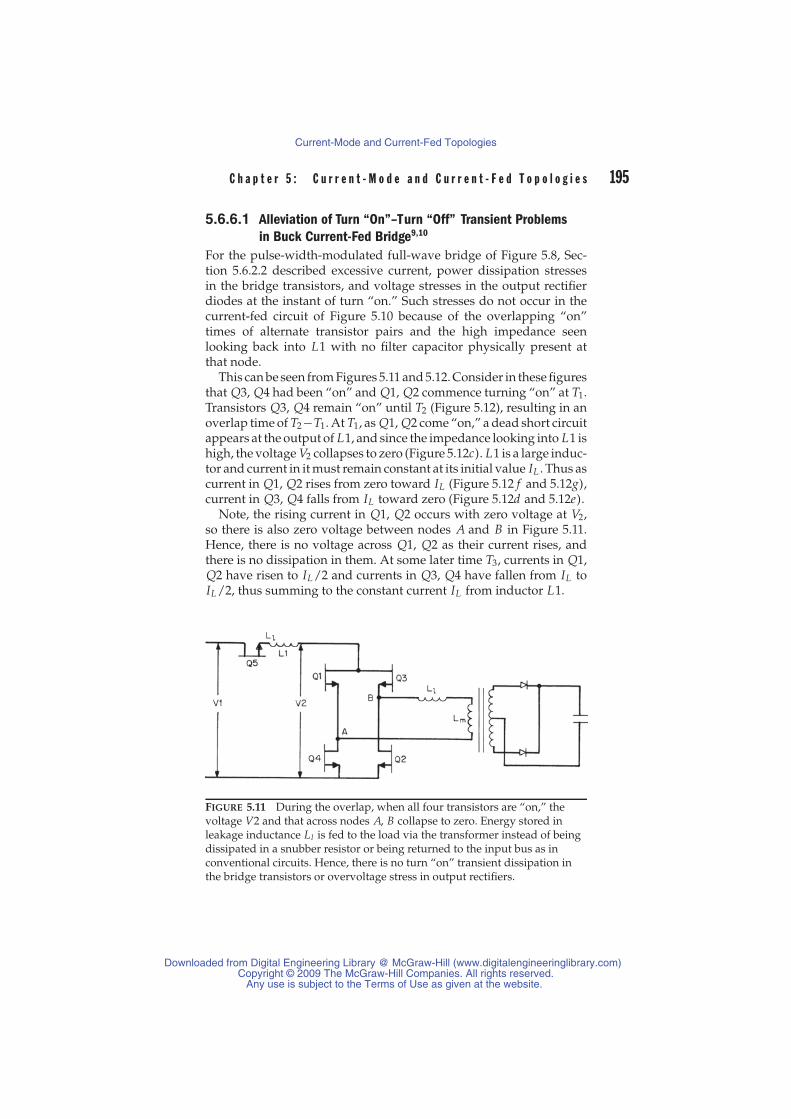
C h a p t e r 5 : C u r r e n t - M o d e a n d C u r r e n t - F e d T o p o l o g i e s 195
5.6.6.1 Alleviation of Turn “On”–Turn “Off” Transient Problemsin Buck Current-Fed Bridge9,10
For the pulse-width-modulated full-wave bridge of Figure 5.8, Sec-tion 5.6.2.2 described excessive current, power dissipation stressesin the bridge transistors, and voltage stresses in the output rectifierdiodes at the instant of turn “on.” Such stresses do not occur in thecurrent-fed circuit of Figure 5.10 because of the overlapping “on”times of alternate transistor pairs and the high impedance seenlooking back into L1 with no filter capacitor physically present atthat node.
This can be seen from Figures 5.11 and 5.12. Consider in these figuresthat Q3, Q4 had been “on” and Q1, Q2 commence turning “on” at T1.Transistors Q3, Q4 remain “on” until T2 (Figure 5.12), resulting in anoverlap time of T2−T1. At T1, as Q1, Q2 come “on,” a dead short circuitappears at the output of L1, and since the impedance looking into L1 ishigh, the voltage V2 collapses to zero (Figure 5.12c). L1 is a large induc-tor and current in it must remain constant at its initial value IL . Thus ascurrent in Q1, Q2 rises from zero toward IL (Figure 5.12 f and 5.12g),current in Q3, Q4 falls from IL toward zero (Figure 5.12d and 5.12e).
Note, the rising current in Q1, Q2 occurs with zero voltage at V2,so there is also zero voltage between nodes A and B in Figure 5.11.Hence, there is no voltage across Q1, Q2 as their current rises, andthere is no dissipation in them. At some later time T3, currents in Q1,Q2 have risen to IL /2 and currents in Q3, Q4 have fallen from IL toIL /2, thus summing to the constant current IL from inductor L1.
FIGURE 5.11 During the overlap, when all four transistors are “on,” thevoltage V2 and that across nodes A, B collapse to zero. Energy stored inleakage inductance Ll is fed to the load via the transformer instead of beingdissipated in a snubber resistor or being returned to the input bus as inconventional circuits. Hence, there is no turn “on” transient dissipation inthe bridge transistors or overvoltage stress in output rectifiers.
Downloaded from Digital Engineering Library @ McGraw-Hill (www.digitalengineeringlibrary.com)Copyright © 2009 The McGraw-Hill Companies. All rights reserved.
Any use is subject to the Terms of Use as given at the website.
Current-Mode and Current-Fed Topologies
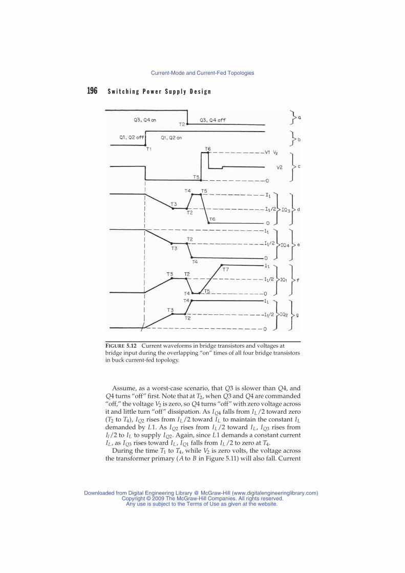
196 S w i t c h i n g P o w e r S u p p l y D e s i g n
FIGURE 5.12 Current waveforms in bridge transistors and voltages atbridge input during the overlapping “on” times of all four bridge transistorsin buck current-fed topology.
Assume, as a worst-case scenario, that Q3 is slower than Q4, andQ4 turns “off” first. Note that at T2, when Q3 and Q4 are commanded“off,” the voltage V2 is zero, so Q4 turns “off” with zero voltage acrossit and little turn “off” dissipation. As IQ4 falls from IL /2 toward zero(T2 to T4), IQ2 rises from IL /2 toward IL to maintain the constant ILdemanded by L1. As IQ2 rises from IL /2 toward IL , IQ3 rises fromIl/2 to IL to supply IQ2. Again, since L1 demands a constant currentIL , as IQ3 rises toward IL , IQ1 falls from IL /2 to zero at T4.
During the time T1 to T4, while V2 is zero volts, the voltage acrossthe transformer primary (A to B in Figure 5.11) will also fall. Current
Downloaded from Digital Engineering Library @ McGraw-Hill (www.digitalengineeringlibrary.com)Copyright © 2009 The McGraw-Hill Companies. All rights reserved.
Any use is subject to the Terms of Use as given at the website.
Current-Mode and Current-Fed Topologies
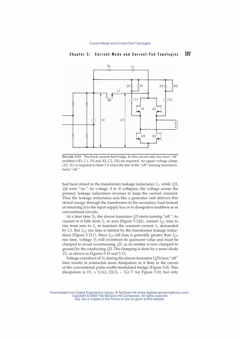
C h a p t e r 5 : C u r r e n t - M o d e a n d C u r r e n t - F e d T o p o l o g i e s 197
FIGURE 5.13 The buck current-fed bridge. In this circuit only two turn “off”snubbers (R1, C1, D1 and R2, C2, D2) are required. An upper voltage clamp(Z1, Dc) is required to limit V2 when the last of the “off”-turning transistorsturns “off.”
had been stored in the transformer leakage inductance L L while Q3,Q4 were “on.” As voltage A to B collapses, the voltage across theprimary leakage inductance reverses to keep the current constant.Thus the leakage inductance acts like a generator and delivers thisstored energy through the transformer to the secondary load insteadof returning it to the input supply bus or to dissipative snubbers as inconventional circuits.
At a later time T5, the slower transistor Q3 starts turning “off.” Ascurrent in it falls from IL to zero (Figure 5.12d), current IQ1 tries torise from zero to IL to maintain the constant current IL demandedby L1. But IQ1 rise time is limited by the transformer leakage induc-tance (Figure 5.12 f ). Since IQ3 fall time is generally greater than IQ1rise time, voltage V2 will overshoot its quiescent value and must beclamped to avoid overstressing Q3, as its emitter is now clamped toground by the conducting Q2. The clamping is done by a zener diodeZ1, as shown in Figures 5.10 and 5.13.
Voltage overshoot of V2 during the slower transistor (Q3) turn “off”time results in somewhat more dissipation in it than in the circuitof the conventional pulse-width-modulated bridge (Figure 5.8). Thisdissipation is (V1 + Vz)( IL/2)(T6 − T5)/T for Figure 5.10, but only
Downloaded from Digital Engineering Library @ McGraw-Hill (www.digitalengineeringlibrary.com)Copyright © 2009 The McGraw-Hill Companies. All rights reserved.
Any use is subject to the Terms of Use as given at the website.
Current-Mode and Current-Fed Topologies

198 S w i t c h i n g P o w e r S u p p l y D e s i g n
V1( IL/2)(T6 − T5)/T for Figure 5.8. In Figure 5.8, there are four tran-sistors that have relatively high turn “off” dissipation. In Figures 5.10and 5.13, only the two transistors with slow turn “off” time have highdissipation. As discussed above, the faster transistor suffers no dissi-pation at turn “off” as it turns “off” at zero voltage; and at turn “on,”all transistors have negligible dissipation, because the transformerleakage inductance is in series with them, so they turn “on” at zerovoltage.
The increased dissipation of the two transistors at turn “off” canbe diverted from the transistors to resistors by adding the snubbingnetworks R1, C1, D1 and R2, C2, D2 of Figure 5.13. Design of suchturn “off” snubbing circuits will be discussed in the later chapter onsnubbers.
5.6.6.2 Absence of Simultaneous Conduction Problemin the Buck Current-Fed Bridge
In the buck voltage-fed bridge of Figure 5.9, care must be taken toavoid simultaneous conduction in transistors positioned verticallyabove one another (Q1, Q4 or Q3, Q2). Such simultaneous conductioncomprises a short circuit across C1. Since C1 has a low impedance, itcan supply large currents without its output (V2) dropping very much.Thus the bridge transistors could be subjected to simultaneous highvoltage and high current, and one or more would immediately fail.
Even if a dead time between the turn “off” of one transistor pair andthe turn “on” of the other is designed in to avoid simultaneous con-duction, it still may occur under various odd circumstances, such ashigh temperature and/or high load conditions when transistor stor-age time may be much lower than data sheets indicate or low inputvoltage (in the absence of maximum “on” time clamp or undervoltagelockout) as the feedback loop increases “on” time to maintain constantoutput voltage.
But in the buck current-fed bridge, simultaneous conduction isactually essential to its operation and the inductor limits the current,hence it provides the advantages discussed above. Further, in the buckcurrent-fed bridge, since the “on” time is slightly more than a halfperiod for each transistor pair, the peak current is less than in thebuck voltage-fed bridge, whose maximum “on” time is usually set at90% of a half period to avoid simultaneous conduction.
5.6.6.3 Turn “On” Problems in Buck Transistorof Buck Current- or Buck Voltage-Fed Bridge10
The buck transistor in either the voltage- or current-fed bridge suffersfrom a large spike of power dissipation at the instant both of turn “on”and turn “off,” as can be seen in Figure 5.14.
Downloaded from Digital Engineering Library @ McGraw-Hill (www.digitalengineeringlibrary.com)Copyright © 2009 The McGraw-Hill Companies. All rights reserved.
Any use is subject to the Terms of Use as given at the website.
Current-Mode and Current-Fed Topologies
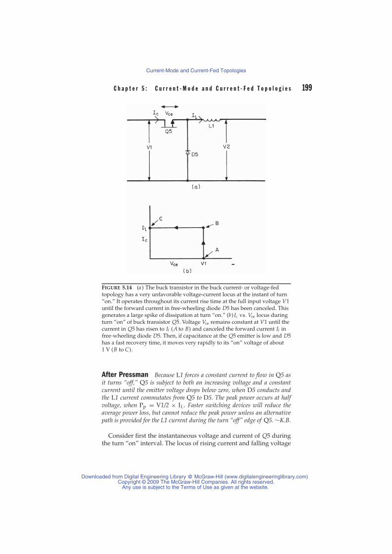
C h a p t e r 5 : C u r r e n t - M o d e a n d C u r r e n t - F e d T o p o l o g i e s 199
FIGURE 5.14 (a ) The buck transistor in the buck current- or voltage-fedtopology has a very unfavorable voltage-current locus at the instant of turn“on.” It operates throughout its current rise time at the full input voltage V1until the forward current in free-wheeling diode D5 has been canceled. Thisgenerates a large spike of dissipation at turn “on.” (b) Ic vs. Vce locus duringturn “on” of buck transistor Q5. Voltage Vce remains constant at V1 until thecurrent in Q5 has risen to Il (A to B) and canceled the forward current Il infree-wheeling diode D5. Then, if capacitance at the Q5 emitter is low and D5has a fast recovery time, it moves very rapidly to its “on” voltage of about1 V (B to C).
After Pressman Because L1 forces a constant current to flow in Q5 asit turns “off,” Q5 is subject to both an increasing voltage and a constantcurrent until the emitter voltage drops below zero, when D5 conducts andthe L1 current commutates from Q5 to D5. The peak power occurs at halfvoltage, when Pp = V1/2 × IL . Faster switching devices will reduce theaverage power loss, but cannot reduce the peak power unless an alternativepath is provided for the L1 current during the turn “off” edge of Q5. ∼K.B.
Consider first the instantaneous voltage and current of Q5 duringthe turn “on” interval. The locus of rising current and falling voltage
Downloaded from Digital Engineering Library @ McGraw-Hill (www.digitalengineeringlibrary.com)Copyright © 2009 The McGraw-Hill Companies. All rights reserved.
Any use is subject to the Terms of Use as given at the website.
Current-Mode and Current-Fed Topologies

200 S w i t c h i n g P o w e r S u p p l y D e s i g n
during that interval is shown in Figure 5.14b. Just prior to Q5 turning“on,” free-wheeling diode D5 is conducting and supplying inductorcurrent IL . As Q5 commences turning “on,” its collector is at V1, itsemitter is at one diode (D5) drop below common. The emitter doesnot move up from common until the current in Q5 has risen from zeroto IL and canceled the D5 forward current.
Thus, during the current rise time to tr , the Ic − Vce locus is frompoints A to B. During tr , the average current supplied by Q5 is IL /2and the voltage across it is V1. Once current in Q5 has risen to IL ,assuming negligible capacitance at the Q5 emitter node and fast re-covery time in D5, the voltage across Q5 rapidly drops to zero alongthe path B to C . If there is one turn “on” of duration tr in a period T ,the dissipation in Q5, averaged over T , is
PDturnon = V1IL tr2T
(5.10)
It is of interest to calculate this dissipation for a 2000-W buck current-fed bridge operating from the rectified 220-V AC line. Nominal recti-fied DC voltage (V1) is about 300 V, minimum is 270 V, and maximumis 330 V. Assume that the bucked-down DC voltage V2 is 25% belowthe minimum V1 or about 200 V.
Further, assume the bridge inverter operates at 80% efficiency, giv-ing an input power of 2500 W. This power comes from a V1 of 200 V,and hence the average current in L1 is 12.5 A. Assume that L1 is largeenough so that the ripple current in IL can be neglected.
Then, for an assumed 0.3-μs current rise time (easily achieved withmodern bipolar transistors) and a Q5 switching frequency of 50 kHz,turn “on” dissipation at maximum AC input voltage is (from Eq. 5.10)
PD = 330(
12.52
)(0.320
)= 31 W
Note in this calculation that the effect of poor recovery time in D5 hasbeen neglected. This has been discussed in Section 5.6.2.2 in connectionwith the poor recovery time of output rectifiers of the bridge inverter.This problem can be far more serious for the free-wheeling diode ofthe buck regulator, for D5 must have a much higher voltage rating—atleast 400 V for the maximum V1 of 330 V—and high-voltage diodeshave poorer recovery times than lower-voltage ones. Thus the Q5current can considerably overshoot the peak of 12.5 A that D5 hadbeen carrying. Further, the oscillatory ring after the recovery time,discussed in Section 5.6.2.2, can cause a serious voltage overstress infree-wheeling diode D5.
Turn “on” dissipation in Q5 and voltage overstress of D5 can beeliminated with the turn “on” snubber of Figure 5.15.
Downloaded from Digital Engineering Library @ McGraw-Hill (www.digitalengineeringlibrary.com)Copyright © 2009 The McGraw-Hill Companies. All rights reserved.
Any use is subject to the Terms of Use as given at the website.
Current-Mode and Current-Fed Topologies
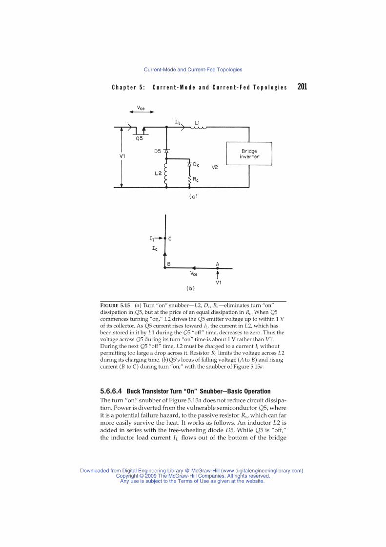
C h a p t e r 5 : C u r r e n t - M o d e a n d C u r r e n t - F e d T o p o l o g i e s 201
FIGURE 5.15 (a ) Turn “on” snubber—L2, Dc , Rc—eliminates turn “on”dissipation in Q5, but at the price of an equal dissipation in Rc . When Q5commences turning “on,” L2 drives the Q5 emitter voltage up to within 1 Vof its collector. As Q5 current rises toward Il , the current in L2, which hasbeen stored in it by L1 during the Q5 “off” time, decreases to zero. Thus thevoltage across Q5 during its turn “on” time is about 1 V rather than V1.During the next Q5 “off” time, L2 must be charged to a current Il withoutpermitting too large a drop across it. Resistor Rc limits the voltage across L2during its charging time. (b)Q5’s locus of falling voltage (A to B) and risingcurrent (B to C) during turn “on,” with the snubber of Figure 5.15a .
5.6.6.4 Buck Transistor Turn “On” Snubber—Basic OperationThe turn “on” snubber of Figure 5.15a does not reduce circuit dissipa-tion. Power is diverted from the vulnerable semiconductor Q5, whereit is a potential failure hazard, to the passive resistor Rs , which can farmore easily survive the heat. It works as follows. An inductor L2 isadded in series with the free-wheeling diode D5. While Q5 is “off,”the inductor load current IL flows out of the bottom of the bridge
Downloaded from Digital Engineering Library @ McGraw-Hill (www.digitalengineeringlibrary.com)Copyright © 2009 The McGraw-Hill Companies. All rights reserved.
Any use is subject to the Terms of Use as given at the website.
Current-Mode and Current-Fed Topologies

202 S w i t c h i n g P o w e r S u p p l y D e s i g n
transistors, up through the bottom end of L2, through free-wheelingdiode D5, and back into the front end of L1. This causes the top endof L2 to be slightly more negative than its bottom end.
As Q5 commences turning “on,” it starts delivering current into thecathode of D5 to cancel its forward current. This current flows downinto L2, opposing the load current it is carrying. Since the current inan inductor (L2) cannot change instantaneously, the voltage polarityacross it reverses instantaneously to maintain constant current.
The voltage at the top end of L2 rises, pushing the free-wheelingdiode cathode up with it until it meets the “on”-turning Q5 emittervoltage. The Q5 emitter is forced up to within Vce(sat) of its collector,and now Q5 continues increasing its current, but at a Vce voltage ofabout 1 V rather than the V1 voltage of 370 V it had to sustain in theabsence of L2.
When the Q5 current has risen to IL (in a time tr ), the forwardcurrent in D5 has been canceled and Q5 continues to supply the loadcurrent IL demanded by L1. Since the voltage across Q5 during therise time tr is only 1 V, its dissipation is negligible. Further, becauseof the high impedance of L2 in series with the D5 anode, there isnegligible recovery time current in D5. The current-voltage locus ofQ5 during the turn “on” time is shown in Figure 5.15b.
5.6.6.5 Selection of Buck Turn “On” Snubber ComponentsFor the preceding sequence of events to proceed as described, thecurrent in L2 must be equal to the load current IL at the start of Q5turn “on” and must have decayed back down to zero in the time tr thatcurrent from Q5 has risen to IL . Since the voltage across L2 during tris clamped to V1, the magnitude of L2 is calculated from
L2 = V1trIL
(5.11)
For the above example, V1 was a maximum of 330 V, tr was 0.3 μs, andIL was 12.5 A. From Eq. 5.11, this yields L2 = 330×0.3/12.5 = 7.9 μH.
The purpose of Rc , Dc in Figure 5.15a is to ensure that at the start ofQ5 turn “on,” current in L2 truly is equal to IL and that it has reachedthat value without overstressing Q5.
Consider, for the moment, that Rc , Dc were not present. As Q5turned “off,” since current in L1 cannot change instantaneously, theinput end of L1 goes immediately negative to keep current constant.If L2 were not present, D5 would clamp the front end of L1 (and hencethe Q5 emitter) at common, and permit a voltage of only V1 across Q5.But with L2 present, the impedance looking out of the D5 anode is thehigh instantaneous impedance of L2. As Q5 turned “off,” IL wouldbe drawn through L2, pulling its top end far negative. This would put
Downloaded from Digital Engineering Library @ McGraw-Hill (www.digitalengineeringlibrary.com)Copyright © 2009 The McGraw-Hill Companies. All rights reserved.
Any use is subject to the Terms of Use as given at the website.
Current-Mode and Current-Fed Topologies

C h a p t e r 5 : C u r r e n t - M o d e a n d C u r r e n t - F e d T o p o l o g i e s 203
a large negative voltage at the Q5 emitter, and with its collector at V1(370 V in this case), it would immediately fail.
Thus Rc and Dc are shunted around L2 to provide a path for IL atthe instant Q5 turns “off,” and Rc is selected low enough so that thevoltage drop across it at a current IL plus V1 is a voltage stress that Q5can safely take. Thus
VQ5(max) = V1 + Rc IL (5.12)
In the preceding example, V1(max) was 330 V. Assume that Q5 had aVceo rating of 450 V. With a t1- to t5-V reverse bias at its base at theinstant of turn “off,” it could safely sustain the Vcev rating of 650 V.Then to provide a margin of safety, select Rc so that VQ5(max) is only450 V. Then from Eq. 5.12, 450 = 330 + Rc × 12.5 or Rc = 9.6�.
5.6.6.6 Dissipation in Buck Transistor Snubber ResistorExamination of Figure 5.15a shows that essentially the constant cur-rent IL is charging the parallel combination of Rc and L2. The Theveninequivalent of this is a voltage source of magnitude IL Rc charging aseries combination of Rc and L2. It is well known that in charging aseries inductor L to a current Ip or energy 1/2L( Ip)2, an equal amountof energy is delivered to the charging resistor. If L is charged to Iponce per period T , the dissipation in the resistor is 1/2L( Ip)2/T .
In the preceding example where T = 2 μs, L = 7.9 μH, and Ip =12.5 A
PDsnubber resistor = (1/2)(7.9)(12.5)2
20= 31 W
Thus, as mentioned above, this snubber has not reduced circuit dissi-pation; it has only diverted it from the transistor Q5 to the snubbingresistor.
5.6.6.7 Snubbing Inductor Charging TimeThe snubbing inductor must be fully charged to IL during the “off”time of the buck transistor. The charging time constant is L/R, whichin the above example is 7.9/6.4 = 1.23 μs. The inductor is 95% fullycharged in three time constants or 3.7 μs.
In the preceding example, switching period T was 20 μs. To buckdown the input of 330 V to the preregulated 200 V, “on” time is Ton =20(200/330) = 12 μs. This leaves a Q5 “off” time of 8 μs, which issufficient, as the snubbing inductor is 95% fully charged in 3.7 μs.
Downloaded from Digital Engineering Library @ McGraw-Hill (www.digitalengineeringlibrary.com)Copyright © 2009 The McGraw-Hill Companies. All rights reserved.
Any use is subject to the Terms of Use as given at the website.
Current-Mode and Current-Fed Topologies
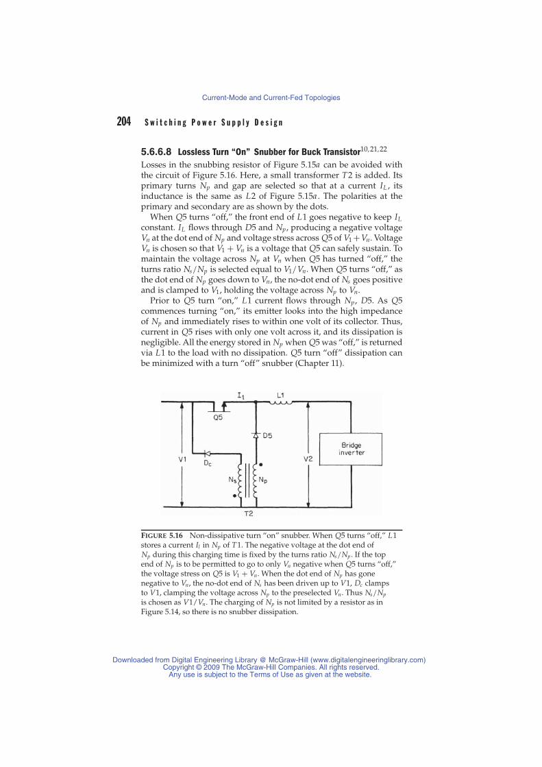
204 S w i t c h i n g P o w e r S u p p l y D e s i g n
5.6.6.8 Lossless Turn “On” Snubber for Buck Transistor10,21,22
Losses in the snubbing resistor of Figure 5.15a can be avoided withthe circuit of Figure 5.16. Here, a small transformer T2 is added. Itsprimary turns Np and gap are selected so that at a current IL , itsinductance is the same as L2 of Figure 5.15a . The polarities at theprimary and secondary are as shown by the dots.
When Q5 turns “off,” the front end of L1 goes negative to keep ILconstant. IL flows through D5 and Np , producing a negative voltageVn at the dot end of Np and voltage stress across Q5 of V1 +Vn. VoltageVn is chosen so that V1 + Vn is a voltage that Q5 can safely sustain. Tomaintain the voltage across Np at Vn when Q5 has turned “off,” theturns ratio Ns/Np is selected equal to V1/Vn. When Q5 turns “off,” asthe dot end of Np goes down to Vn, the no-dot end of Ns goes positiveand is clamped to V1, holding the voltage across Np to Vn.
Prior to Q5 turn “on,” L1 current flows through Np , D5. As Q5commences turning “on,” its emitter looks into the high impedanceof Np and immediately rises to within one volt of its collector. Thus,current in Q5 rises with only one volt across it, and its dissipation isnegligible. All the energy stored in Np when Q5 was “off,” is returnedvia L1 to the load with no dissipation. Q5 turn “off” dissipation canbe minimized with a turn “off” snubber (Chapter 11).
FIGURE 5.16 Non-dissipative turn “on” snubber. When Q5 turns “off,” L1stores a current Il in Np of T1. The negative voltage at the dot end ofNp during this charging time is fixed by the turns ratio Ns/Np . If the topend of Np is to be permitted to go to only Vn negative when Q5 turns “off,”the voltage stress on Q5 is V1 + Vn. When the dot end of Np has gonenegative to Vn, the no-dot end of Ns has been driven up to V1, Dc clampsto V1, clamping the voltage across Np to the preselected Vn. Thus Ns/Np
is chosen as V1/Vn. The charging of Np is not limited by a resistor as inFigure 5.14, so there is no snubber dissipation.
Downloaded from Digital Engineering Library @ McGraw-Hill (www.digitalengineeringlibrary.com)Copyright © 2009 The McGraw-Hill Companies. All rights reserved.
Any use is subject to the Terms of Use as given at the website.
Current-Mode and Current-Fed Topologies

C h a p t e r 5 : C u r r e n t - M o d e a n d C u r r e n t - F e d T o p o l o g i e s 205
5.6.6.9 Design Decisions In Buck Current-Fed BridgeThe first decision to be made on the buck current-fed bridge is whento use it. It is primarily a high-output-power, high-output-voltagetopology.
In terms of cost, efficiency, and required space, it is a good choicefor output powers in the range of 1 to 10 or possibly 20 kW. For high-output voltages—above about 200 V—and above about 5 A outputcurrent—the absence of output inductors makes it a good choice. Foroutput powers above 1 kW, the added dissipation, volume, and cost ofthe buck transistor is not a significant increase above what is requiredin a competing topology such as a pulse-width-modulated full-wavebridge.
It is an especially good choice for a multi-output supply consistingof one or more high-output voltages (5000 to 30,000 V). In such appli-cations, the absence of output inductors permits the use of capacitor-diode voltage multiplier chains.8,13 Also, the absence of outputinductors in the associated lower-output voltages partly compensatesfor the cost and volume of the buck transistor and its output inductor.
The next design decision is the selection of the bucked-down voltage(V2 of Figure 5.10). This is chosen at about 25% below the lowest rippletrough of V1 (Figure 5.10) at the lowest specified AC input. InductorL1 is chosen for continuous operation at the calculated minimuminductor current IL corresponding to the minimum total output powerat the preselected value of V2. It is chosen as in Section 1.3.6 for aconventional buck regulator.
The output capacitors are not chosen to provide storage or reduceripple directly at the output, because the overlapping conduction ofbridge transistors minimizes this requirement. Rather they are chosenso that when reflected into the primary, the equivalent series resis-tance Resr of all reflected capacitors is sufficiently low as to minimizeripple at V2. Recall from Section 1.3.7, in calculating the magnitude ofthe output capacitor, it was pointed out that output ripple in a buckregulator Vbr is given by
Vbr = �I Resr
in which �I is the peak-to-peak ripple current in the buck inductorand is usually set at twice the minimum DC current in it so that theinductor is on the threshold of discontinuous operation at its mini-mum DC current. Minimum DC current in this case is the current atminimum specified output power at the preselected value of V2. Thuswith Resr selected so as to yield the desired ripple at V2, ripple at eachsecondary is
Vsr = VbrNs
Np
Downloaded from Digital Engineering Library @ McGraw-Hill (www.digitalengineeringlibrary.com)Copyright © 2009 The McGraw-Hill Companies. All rights reserved.
Any use is subject to the Terms of Use as given at the website.
Current-Mode and Current-Fed Topologies

206 S w i t c h i n g P o w e r S u p p l y D e s i g n
There is an interesting contrast in comparing a current- to a voltage-fed bridge at the same bucked-down voltage (V2 of Figures 5.9and 5.10).
For the voltage-fed bridge, a maximum “on” time of 80% of a halfperiod must be established to ensure that there is no simultaneousconduction in the two transistors positioned vertically one above an-other. With the low impedance looking back into the buck regulator ofthe voltage-fed circuit, such simultaneous conduction would subjectthe bridge transistors to high voltage and high current and destroyone or more of them.
In the current-fed circuit, such slightly overlapping simultaneousconduction is essential to its operation and “on” time of alternatetransistor pairs is slightly more than a full half period at any DCinput voltage. In addition, since the “on” time of a voltage-fed bridge(Figure 5.9) is only 80% of a half period, its peak current must be 20%greater than that of the current-fed bridge at the same output power.
It should also be noted that the number of primary turns as calcu-lated from Faraday’s law (Eq. 2.7) must be 20% greater in the current-fed bridge, since the “on” time is 20% greater for a flux change equalto that in a voltage-fed bridge at the same V2.
5.6.6.10 Operating Frequencies—Buck and Bridge TransistorsThe buck transistor is usually synchronized to and operates at twicethe square-wave switching frequency of the bridge transistors. Recallthat it alone is pulse-width-modulated, and that the bridge devicesare operated at a 50-percent duty cycle with a slightly overlapping“on” time.
Frequently, however, the scheme of Figure 5.17a with two buck tran-sistors (Q5A and Q5B) is used to reduce dissipation. They are syn-chronized to the bridge transistor frequency and are turned “on” andpulse-width-modulated on alternate half cycles of the bridge square-wave frequency. Thus the DC and switching losses are shared betweentwo transistors with a resulting increase in reliability.
5.6.6.11 Buck Current-Fed Push-Pull TopologyThe buck current-fed circuit can also be used to drive a push-pullcircuit as in Figure 5.18 with the consequent saving of two transistorsover the buck current-fed bridge. Most of the advantages of the buckcurrent-fed bridge are realized and the only disadvantage is that thepush-pull circuit power transistors have greater voltage stress. Thisvoltage stress is twice V2, rather than V2 as in the bridge circuit. But V2is the pre-regulated and bucked-down input voltage—usually only75% of the minimum V1 input. This is usually about the same as themaximum DC input of a competing topology—like the pulse-width-modulated full-wave bridge (Figure 5.8).
Downloaded from Digital Engineering Library @ McGraw-Hill (www.digitalengineeringlibrary.com)Copyright © 2009 The McGraw-Hill Companies. All rights reserved.
Any use is subject to the Terms of Use as given at the website.
Current-Mode and Current-Fed Topologies
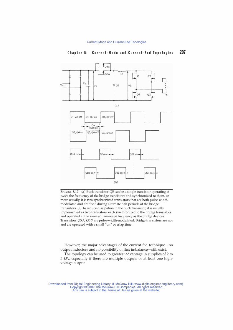
C h a p t e r 5 : C u r r e n t - M o d e a n d C u r r e n t - F e d T o p o l o g i e s 207
FIGURE 5.17 (a ) Buck transistor Q5 can be a single transistor operating attwice the frequency of the bridge transistors and synchronized to them, ormore usually, it is two synchronized transistors that are both pulse-width-modulated and are “on” during alternate half periods of the bridgetransistors. (b) To reduce dissipation in the buck transistor, it is usuallyimplemented as two transistors, each synchronized to the bridge transistorsand operated at the same square-wave frequency as the bridge devices.Transistors Q5A, Q5B are pulse-width-modulated. Bridge transistors are notand are operated with a small “on” overlap time.
However, the major advantages of the current-fed technique—nooutput inductors and no possibility of flux imbalance—still exist.
The topology can be used to greatest advantage in supplies of 2 to5 kW, especially if there are multiple outputs or at least one high-voltage output.
Downloaded from Digital Engineering Library @ McGraw-Hill (www.digitalengineeringlibrary.com)Copyright © 2009 The McGraw-Hill Companies. All rights reserved.
Any use is subject to the Terms of Use as given at the website.
Current-Mode and Current-Fed Topologies
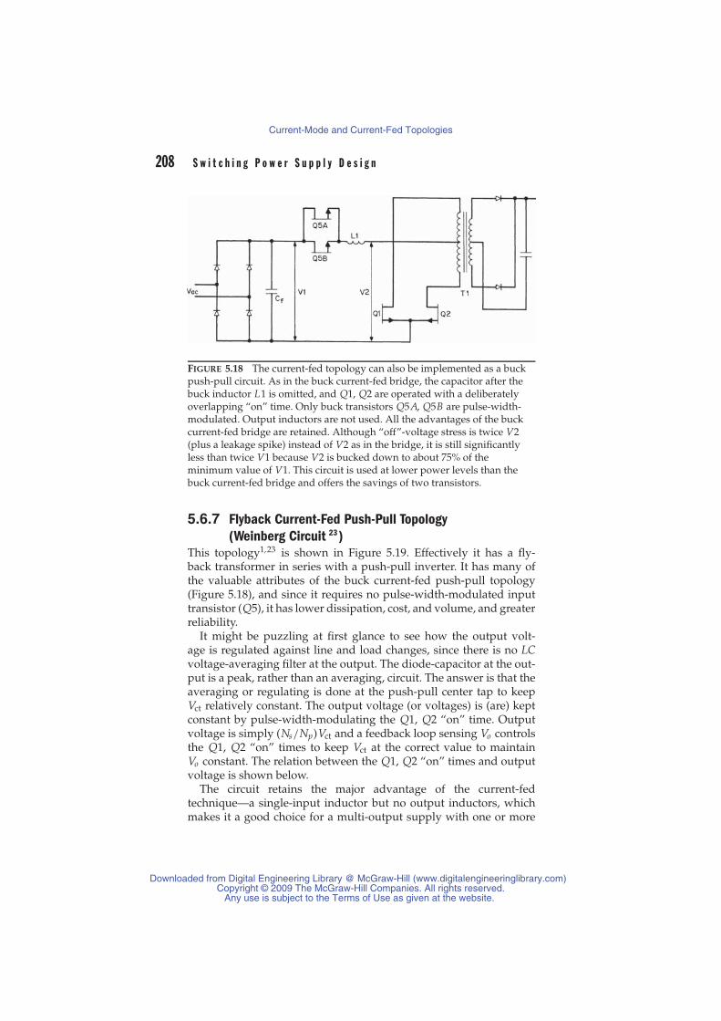
208 S w i t c h i n g P o w e r S u p p l y D e s i g n
FIGURE 5.18 The current-fed topology can also be implemented as a buckpush-pull circuit. As in the buck current-fed bridge, the capacitor after thebuck inductor L1 is omitted, and Q1, Q2 are operated with a deliberatelyoverlapping “on” time. Only buck transistors Q5A, Q5B are pulse-width-modulated. Output inductors are not used. All the advantages of the buckcurrent-fed bridge are retained. Although “off”-voltage stress is twice V2(plus a leakage spike) instead of V2 as in the bridge, it is still significantlyless than twice V1 because V2 is bucked down to about 75% of theminimum value of V1. This circuit is used at lower power levels than thebuck current-fed bridge and offers the savings of two transistors.
5.6.7 Flyback Current-Fed Push-Pull Topology(Weinberg Circuit 23)
This topology1,23 is shown in Figure 5.19. Effectively it has a fly-back transformer in series with a push-pull inverter. It has many ofthe valuable attributes of the buck current-fed push-pull topology(Figure 5.18), and since it requires no pulse-width-modulated inputtransistor (Q5), it has lower dissipation, cost, and volume, and greaterreliability.
It might be puzzling at first glance to see how the output volt-age is regulated against line and load changes, since there is no LCvoltage-averaging filter at the output. The diode-capacitor at the out-put is a peak, rather than an averaging, circuit. The answer is that theaveraging or regulating is done at the push-pull center tap to keepVct relatively constant. The output voltage (or voltages) is (are) keptconstant by pulse-width-modulating the Q1, Q2 “on” time. Outputvoltage is simply (Ns/Np)Vct and a feedback loop sensing Vo controlsthe Q1, Q2 “on” times to keep Vct at the correct value to maintainVo constant. The relation between the Q1, Q2 “on” times and outputvoltage is shown below.
The circuit retains the major advantage of the current-fedtechnique—a single-input inductor but no output inductors, whichmakes it a good choice for a multi-output supply with one or more
Downloaded from Digital Engineering Library @ McGraw-Hill (www.digitalengineeringlibrary.com)Copyright © 2009 The McGraw-Hill Companies. All rights reserved.
Any use is subject to the Terms of Use as given at the website.
Current-Mode and Current-Fed Topologies
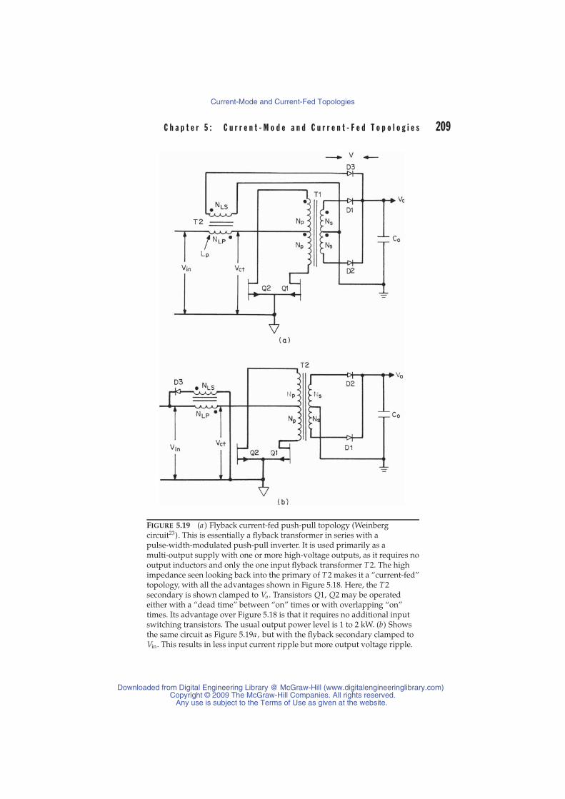
C h a p t e r 5 : C u r r e n t - M o d e a n d C u r r e n t - F e d T o p o l o g i e s 209
FIGURE 5.19 (a ) Flyback current-fed push-pull topology (Weinbergcircuit23). This is essentially a flyback transformer in series with apulse-width-modulated push-pull inverter. It is used primarily as amulti-output supply with one or more high-voltage outputs, as it requires nooutput inductors and only the one input flyback transformer T2. The highimpedance seen looking back into the primary of T2 makes it a “current-fed”topology, with all the advantages shown in Figure 5.18. Here, the T2secondary is shown clamped to Vo . Transistors Q1, Q2 may be operatedeither with a “dead time” between “on” times or with overlapping “on”times. Its advantage over Figure 5.18 is that it requires no additional inputswitching transistors. The usual output power level is 1 to 2 kW. (b) Showsthe same circuit as Figure 5.19a, but with the flyback secondary clamped toVin. This results in less input current ripple but more output voltage ripple.
Downloaded from Digital Engineering Library @ McGraw-Hill (www.digitalengineeringlibrary.com)Copyright © 2009 The McGraw-Hill Companies. All rights reserved.
Any use is subject to the Terms of Use as given at the website.
Current-Mode and Current-Fed Topologies

210 S w i t c h i n g P o w e r S u p p l y D e s i g n
high-voltage outputs. Further, because of the high-source impedanceof the flyback transformer primary L1, the usual flux-imbalance prob-lem of voltage-fed push-pulls does not result in transformer saturationand consequent transistor failure. Its major usage is at the 1- to 2-kWpower level.
Two circuit configurations of the flyback current-fed push-pulltopology are shown in Figure 5.19a and 5.19b. Figure 5.19a showsthe flyback secondary returned to the output voltage through diodeD3; in Figure 5.19b, the diode is returned to the input voltage. Whenthe diode is returned to Vo , output ripple voltage is minimized; whenit is returned to Vin, input ripple current is minimized. Consider firstthe configuration of Figure 5.19a, where the diode is returned to theoutput.
The configuration of Figure 5.19a can operate in two significantlydifferent modes. In the first mode, Q1 and Q2 are never permitted tohave overlapping “on” times at any DC input voltage. In the secondmode, Q1 and Q2 may have overlapping “on” times throughout theentire range of specified DC input voltage. The circuit can also be setup to shift between the two modes under control of the feedback loopas the input voltage varies.
It will be shown below that in the non-overlapping mode, power isdelivered to the secondaries at a center tap voltage Vct lower than theDC input voltage (buck-like operation) and in the overlapping mode,power is delivered to the secondaries at a center tap voltage Vct higherthan the DC input voltage (boost-like operation). Since Vct is relativelylow in the non-overlapping mode, Q1, Q2 currents are relatively highfor a given output power. But with the lower Vct voltage, “off”-voltagestress in Q1, Q2 is relatively low. In the overlapping mode, since Vct ishigher than Vin, Q1, Q2 currents are lower for a given output powerbut “off”-voltage stress in Q1, Q2 is higher than that for the non-overlapping mode.
The circuit is usually designed not to remain in one mode through-out the full range of input voltages. Rather, it is designed to operate inthe overlapping mode with an “on” duty cycle Ton/T greater than 0.5,and in the non-overlapping mode with Ton/T less than 0.5 as the DCinput voltage shifts from its minimum to its maximum specified val-ues. This permits proper operation throughout a larger range of DCinput voltages than if operation remained within one mode through-out the entire range of DC input voltage.
5.6.7.1 Absence of Flux-Imbalance Problemin Flyback Current-Fed Push-Pull Topology
Flux imbalance is not a serious problem in this topology because ofthe high-impedance current-fed source that feeds the push-pull trans-former center tap.
Downloaded from Digital Engineering Library @ McGraw-Hill (www.digitalengineeringlibrary.com)Copyright © 2009 The McGraw-Hill Companies. All rights reserved.
Any use is subject to the Terms of Use as given at the website.
Current-Mode and Current-Fed Topologies

C h a p t e r 5 : C u r r e n t - M o d e a n d C u r r e n t - F e d T o p o l o g i e s 211
The current-fed nature of the circuit arises from the flyback trans-former, which is in series with the push-pull center tap. The highimpedance looking back from the push-pull center tap is the magne-tizing inductance of the flyback primary.
In a conventional voltage-fed push-pull inverter, unequal volt-second products across the two half primaries cause the flux-imbalance problem (Section 2.2.5). The transformer core moves offcenter of its hysteresis loop and toward saturation. Because of the lowimpedance of a voltage source, current to the push-pull center tap isunlimited and the voltage at that point (Vct) remains high. The corethen moves further into saturation, where its impedance eventuallyvanishes and transistor currents increase drastically. With high currentand voltage, the transistors will fail.
With the high impedance looking back into the dot end of NLPas shown in Figure 5.19, however, as the push-pull core moves intosaturation drawing more current, the high current causes a voltagedrop at Vct. This reduces the volt-second product on the half pri-mary, which is moving toward saturation, and prevents complete coresaturation.
Thus the high source impedance of NLP does not fully prevent coresaturation. In the worst case, it keeps the core close to the knee ofthe BH loop, which is sufficient to keep transistor currents from ris-ing to disastrous levels. The major drawback of push-pull circuit fluximbalance is thus not a problem with this inverter.
5.6.7.2 Decreased Push-Pull Transistor Currentin Flyback Current-Fed Topology
In a conventional pulse-width-modulated push-pull, driven at thecenter tap from a low-impedance voltage source, it is essential to avoidsimultaneous conduction in the transistors by providing a dead timeof about 20% of a half period between turn “off” of one transistor andturn “on” of the other. This results in higher peak transistor current forthe same output power, since output power is proportional to averagetransistor current.
This dead time is essential in the voltage-fed push-pull, for if Q1, Q2were simultaneously “on,” the half primaries could not sustain volt-age. Then, the transistor collectors would rise to the supply voltage,which would remain high, and with high voltage and high current,the transistors would fail.
In the current-fed circuit, there is no problem if both transistors aresimultaneously “on” under transient or fault conditions, when theDC input voltage is momentarily lower than specified or with storagetimes greater than specified, because of the high impedance lookingback into the dot end of NLP. Should both transistors turn “on” briefly
Downloaded from Digital Engineering Library @ McGraw-Hill (www.digitalengineeringlibrary.com)Copyright © 2009 The McGraw-Hill Companies. All rights reserved.
Any use is subject to the Terms of Use as given at the website.
Current-Mode and Current-Fed Topologies