Embed Size (px)
Citation preview
Nanofabrication Advances for High Efficiency Critical-AngleTransmission Gratings
Alexander R. Bruccoleria, Dong Guana, Ralf K. Heilmanna, Steve Vargob, Frank DiPiazzac
and Mark L. Schattenburga
aSpace Nanotechnology Laboratory, MIT Kavli Institute for Astrophysics and Space Research,Massachusetts Institute of Technology, Cambridge, MA 02139, USA;
bSPTS Technologies, Inc., 1150 Ringwood Ct., San Jose, CA 95131, USA;cSilicon Resources LLC, 1158 Blue Heron, Highland, MI 48357, USA
ABSTRACT
We report several break-through nanofabrication developments enabling high efficiency and high resolving powerspectrometers in the soft x-ray band. The device is the critical-angle transmission (CAT) grating, which com-bines the low mass and relaxed alignment tolerances of a transmission grating with the high broad-band efficiencyand high diffraction orders of a blazed reflection grating. Past work successfully demonstrated the CAT grat-ing concept; however, the open-area fraction was often less than 20% whilst more than 50% is desired. Thispresents numerous nanofabrication challenges including a requirement for a freestanding silicon membrane ofultra high-aspect ratio bars at a period of 200 nanometers with minimal cross support blockage. Furthermore,the sidewalls must be smooth to a few nanometers to efficiently reflect soft x-rays. We have developed a completenanofabrication process for creating freestanding CAT gratings via plasma-etching silicon wafers with a buriedlayer of SiO2. This removable buried layer enables combining a record-performance plasma etch for the CATgrating with a millimeter-scale honeycomb structural support to create a large-area freestanding membrane. Wehave also developed a process for polishing sidewalls of plasma-etched ultra-high aspect ratio nanoscale siliconstructures via potassium hydroxide (KOH). This process utilizes the anisotropic etch nature of single crystalsilicon in KOH. We developed a novel alignment technique to align the CAT grating bars to the {111} planes ofsilicon within 0.2 degrees, which enables KOH to etch away sidewall roughness without destroying the structure,since the {111} planes etch approximately 100 times slower than the non-{111} planes. Preliminary results of acombined freestanding grating with polishing are presented to enable efficient diffraction of soft x-rays.
Keywords: Soft X-ray Diffraction, Blazed Grating, CAT Grating, DRIE, MEMS, KOH Polishing, ChemicalPolishing, Interference Lithography, Pattern Transfer
1. INTRODUCTION
This paper presents progress on fabricating ultra-high aspect ratio freestanding gratings on the nanoscale forsoft x-ray spectroscopy as described in detail by Bruccoleri.1–3 Specifically, referred to as the critical-angletransmission (CAT) grating, it is targeted towards high-efficiency space-based x-ray spectrometers with highphoton throughput due to its large size and high open-area fraction. The soft x-ray band with energies below1 keV is of interest, covering the emission lines of nitrogen, oxygen, carbon, iron and neon.4 In addition, otherpotential applications include ultraviolet filtration,5 phase contrast imaging6 and neutral mass spectroscopy.7
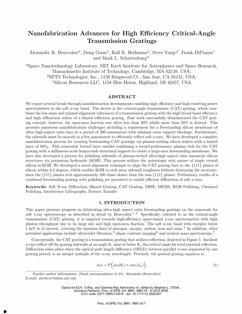
Conceptually, the CAT grating is a transmission grating that utilizes reflection, depicted in Figure 1. Incidentx-rays reflect off the grating sidewalls at an angle θi, near or below θc, the critical angle for total external reflection.Diffraction takes place when the optical path length difference (OPLD) between parallel x-rays separated by onegrating period, is an integer multiple of the x-ray wavelength. Precisely, the general grating equation is:
mλ = P(sin(θi) + sin(βm)
), (1)
Further author information: (Send correspondence to Dr. Alexander Bruccoleri)E-mail: [email protected]
Optics for EUV, X-Ray, and Gamma-Ray Astronomy VI, edited by Stephen L. O'Dell, Giovanni Pareschi, Proc. of SPIE Vol. 8861, 886119 · © 2013 SPIE
CCC code: 0277-786X/13/$18 · doi: 10.1117/12.2024357
Proc. of SPIE Vol. 8861 886119-1
Downloaded From: http://proceedings.spiedigitallibrary.org/ on 10/17/2013 Terms of Use: http://spiedl.org/terms
Depth, L
Period, P
v -
Width, w
i--A; il
r
¡ ßm'I .
Ot" Order W OPLD
where m is an integer designating the diffraction order, P is the grating period, βm is the angle of the outgoingdiffraction orders, θi is the angle of incidence and λ is the wavelength.
Figure 1: Conceptual drawing of x-ray diffraction and condition for total external reflection. (Not to scale.)
The x-rays enter the grating at a shallow graze angle relative to the grating bar sidewalls where they re-flect with minimal absorption and maximum efficiency occurs when βm is equal to θi. This blazing effect cansignificantly increase efficiency since the majority of the x-rays are directed into a small number of non-zerodiffraction orders. The state-of-the-art in space-based phase-shifting x-ray transmission gratings are the gold-on-a-membrane gratings onboard the Chandra x-ray telescope. The gold bars absorb soft x-rays, reducing thegratings’ efficiency.8,9 The CAT grating avoids the majority of the absorption losses by reflecting the majorityof the x-rays, increasing the soft x-ray efficiency by a factor up to five over the Chandra gratings.10
The x-rays must reflect at or below the critical angle for total external reflection θc, to be efficient, (θc ≈√2δ).11 For silicon θc is a very shallow angle, ≈ 1.6◦, for λ of 1 nm, which leads to the required ultra-high aspect
ratio for CAT grating bars. For efficient x-ray reflectivity the surfaces also have to be smooth. The efficiency ofreflection is,
R(q) = Roe−q2σ2
, (2)
an exponential function of roughness, where R is the reflectivity, Ro is the reflectivity from a perfectly smoothsurface, q is the momentum transfer of the reflection and σ is the roughness. The momentum transfer from aspecular x-ray reflection is,
q =4π
λn sin θ, (3)
Proc. of SPIE Vol. 8861 886119-2
Downloaded From: http://proceedings.spiedigitallibrary.org/ on 10/17/2013 Terms of Use: http://spiedl.org/terms

where θ is the angle of grazing incidence and n is the index of refraction of the material for the incident x-ray.In order to achieve R/Ro ≈ 90% for a soft x-ray, λ of 1 nm, with a grazing incidence angle of 1.6◦, the roughnessneeds to be on the order of 1 nm.
The specific geometry and dimensions for CAT gratings are set by the desired spectral band and telescopedesign. The current point-design has a 200-nm grating period, depth of 4 μm, bar width of 40 nm and surfaceroughness of the grating bars on the order of 1 nm. The goal is to provide > 50% diffraction efficiency forwavelengths between 2-7 nm for missions such as the Advanced X-ray Spectroscopy and Imaging Observatory(AXSIO) and the Square Meter Arcsecond Resolution X-ray Telescope (SMART-X ).12,13
The fabrication processes developed by Bruccoleri et al. and summarized here successfully demonstratedgratings with the desired period and depth, with a net open-area fraction including all structural supports onthe order of 30%, and spans of 31 mm on a side.1 This is more than a factor of two improvement in aspectratio of previous work on freestanding nanoscale gratings.14 The fabrication process utilizes silicon-on-insulator(SOI) wafers and features integrated structural supports in the handle and device layers, referred to as Level1 and Level 2 supports, respectively. The process utilizes deep reactive-ion etching (DRIE) for both the CATgrating and Level 1 supports in the SOI device and Level 2 supports in the handle layer, which allows for crystallattice independent etching.15 The main drawback of the process was the grating sidewalls were unpolished andlikely not suitable for efficient reflection. To address the roughness a polishing process with potassium hydroxide(KOH) was developed by Bruccoleri et al. and summarized here.3 This polishing process reduced the RMSroughness as measured with an AFM from 4 nm to 1 nm. Furthermore the width of the CAT grating bars werereduced from 100 nm to 70 nm. These features are over 30 times smaller than previously DRIE-KOH polishedfeatures published to date.16,17 A combined process has been developed to create a freestanding grating withnarrow and smooth sidewalls. The combined process is preliminary, and further refinement is required to improvethe strength of the device.
2. FABRICATION METHODOLOGY
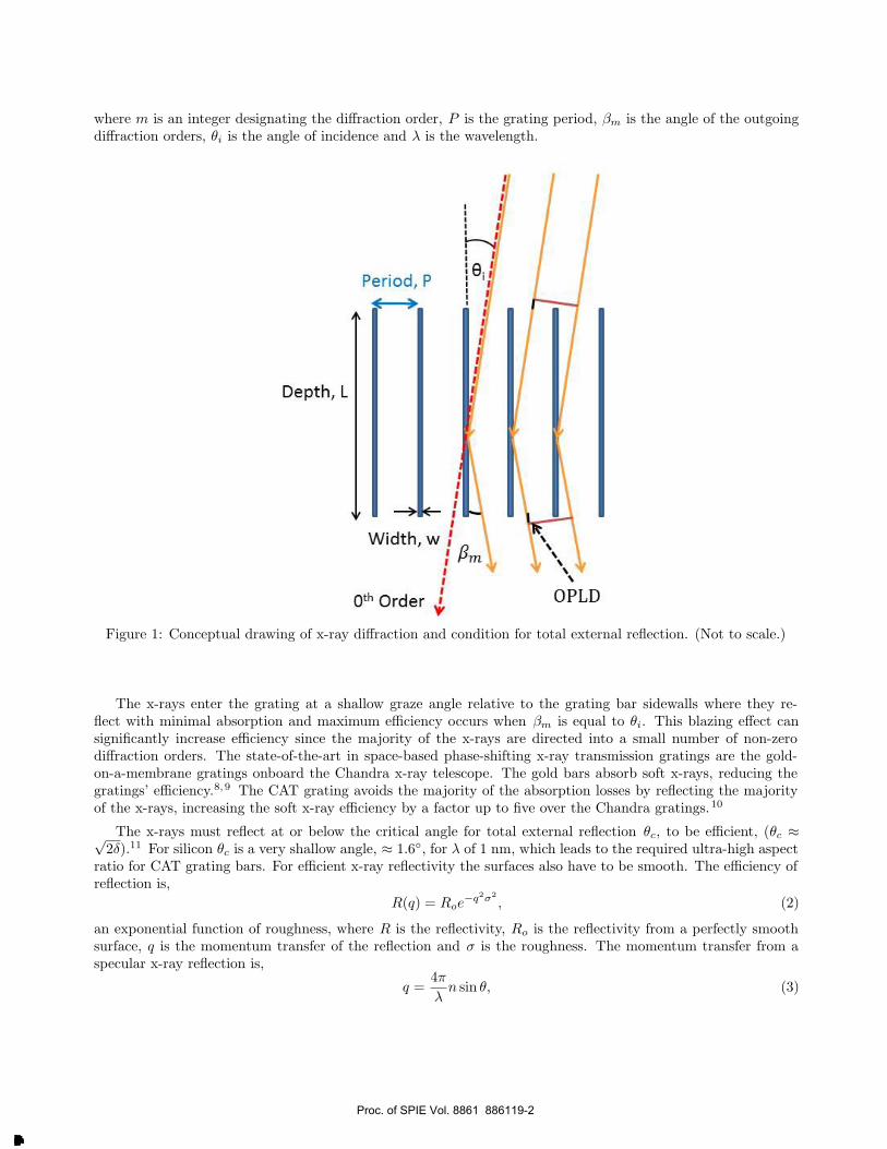
The fabrication methodology developed for freestanding gratings is based on integrated front and back sideDRIE steps on SOI wafers (see Figure 2). A 4 μm-thick device layer is used for both the CAT grating and anintegrated 5 μm-period cross support mesh designated ”Level 1”. A 500 μm handle layer serves as the large-areastructural support designated ”Level 2”. The 500 nm-thick buried SiO2 layer acts as an etch stop for both etches.The general fabrication procedure is as follows: After substrate preparation (1), the mask for the back side ispatterned followed by front side masking (2). The front side is then deep-etched (3), filled and protected (4),flipped over and bonded to a carrier wafer. The back side is then deep-etched (5), the buried layer removed (6),and the sample is separated from the carrier, cleaned and critical-point dried to finish (7).
Proc. of SPIE Vol. 8861 886119-3
Downloaded From: http://proceedings.spiedigitallibrary.org/ on 10/17/2013 Terms of Use: http://spiedl.org/terms
IIIIIIIIIIIIIIIHIIIIIIIIIIIIIIII
Device Silicon (4 im)400 nm thermal SiO2
e> " """ """ 500 nm buried Si02
Bulk Silicon (500 µm)
PECVD SiO2 (411m)
1. Start with SOI wafer
11 11111 111 1 1 11 1 1 Locate {111} planes
\\ \ \ \
2. Pattern front and back side SiO-
r /ts.\ \\ \ \ \ \ \\ \ \ \ \ \ \ \ \ \ \ \\ \ \ \ \
e
IRMO5. Flip over, bond to carrierwafer with crystal bond under
Align to {111} planes vacuum
11111111111111111 Two opportunities toNal
111111101111111111 polish
3. DRIE front side and stop on SiO
11111111 111 11111 1Phctoresist (10 µm)
11111111111111111
4. Fill front side gratings with hphotoresist
i
6. Wet HF etch buried SiO2
IIIIIIIIIIIIIIIII
7. De -bond from carrier, cleanphotoresist, critical -point dry andash
Figure 2: Process flow chart. The bold arrows are for future steps that integrate KOH polishing.
2.1 Freestanding Grating
The front side is masked with 400 nm of thermal SiO2 and etched via the Bosch DRIE process in an STPS Pegasustool as demonstrated in past work.18 The 200 nm-period CAT grating is patterned via interference lithography(IL),19 and transferred into the thermal SiO2 layer via a tri-layer stack.20 See Figure 3 for a scanning electronmicroscope (SEM) image of the 200 nm-period mask. The key step after deep etching the CAT grating is thephotoresist-fill process of the CAT grating bars. The specific process is to apply two coatings of PFI-88A7photoresist (Sumitomo Corporation) and one coat of AZ 4620 photoresist (AZ Electronic Materials). Both
Proc. of SPIE Vol. 8861 886119-4
Downloaded From: http://proceedings.spiedigitallibrary.org/ on 10/17/2013 Terms of Use: http://spiedl.org/terms

illllllllllllllllll {'ii
es
Bulk Silicon
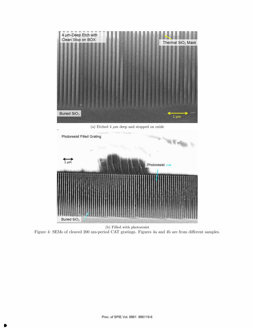
photoresist are spin coated at at 3000 rpm, placed in vacuum (≈ 0.25 atm) for outgassing and hotplate bakedat 90◦ C for 60 seconds. The sample can be bonded to a carrier wafer via Crystalbond 555 (Structural Probe,Inc.) for back side etching since the CAT grating is filled and protected. See Figure 4 for SEM images of thedeep-etch and the filled 4 μm deep grating.
The back side etch for the Level 2 structure is also performed with a Bosch process which stops on the sameburied SiO2 as the front side. The etch mask is 4 μm PECVD SiO2 and 400 nm thermal SiO2. The Level 2structure is comprised of an array of 1 mm-wide hexagons with 100 μm-wide lines, spanning 31 mm on a side.See Figure 5 for a SEM image of the hexagon array. The buried SiO2 is removed with a wet HF etch following theback side etch. The sample is removed from the carrier by immersing it in water at ≈ 80◦ C until the Crystalbondmelts and the sample floats free. The photoresist filling is cleaned from the grating channels with two successivepiranha cleans. The grating cannot be dried in air, since surface tension will pull the bars together. Insteadthe sample is kept submerged and critical-point dried to avoid the formation of liquid-air interfaces. Finally, thesample is placed in an asher (isotropic O2 plasma) to clean any remaining organic material between the gratingbars. The result is a fully integrated freestanding CAT grating structure (see Figure 6).
Figure 3: Top down SEM of a two-dimensional 200 nm-period thermal SiO2 mask.
Proc. of SPIE Vol. 8861 886119-5
Downloaded From: http://proceedings.spiedigitallibrary.org/ on 10/17/2013 Terms of Use: http://spiedl.org/terms
Photoresist
Photoresist Filled Grating
1 1
4 pm -Deep Etch withClean Stop on BOX awe iii 1
Thermal Si02 Mask
(a) Etched 4 μm deep and stopped on oxide
(b) Filled with photoresist
Figure 4: SEMs of cleaved 200 nm-period CAT gratings. Figures 4a and 4b are from different samples.
Proc. of SPIE Vol. 8861 886119-6
Downloaded From: http://proceedings.spiedigitallibrary.org/ on 10/17/2013 Terms of Use: http://spiedl.org/terms

Grating
Film
Figure 5: SEM from the bottom side of the hexagon support structure and grating film.
Proc. of SPIE Vol. 8861 886119-7
Downloaded From: http://proceedings.spiedigitallibrary.org/ on 10/17/2013 Terms of Use: http://spiedl.org/terms

"mama
5 µm -pitch level 1 lisupport grating
200 nm -pitch cleavedgrating bars
(a)
(b)
Figure 6
Proc. of SPIE Vol. 8861 886119-8
Downloaded From: http://proceedings.spiedigitallibrary.org/ on 10/17/2013 Terms of Use: http://spiedl.org/terms
/ MEW-Photograph of Gratina Film next to US Quarter
(c)
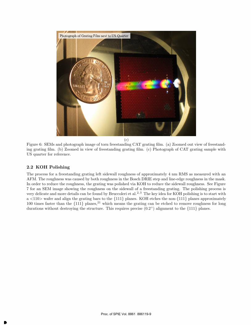
Figure 6: SEMs and photograph image of torn freestanding CAT grating film. (a) Zoomed out view of freestand-ing grating film. (b) Zoomed in view of freestanding grating film. (c) Photograph of CAT grating sample withUS quarter for reference.
2.2 KOH Polishing
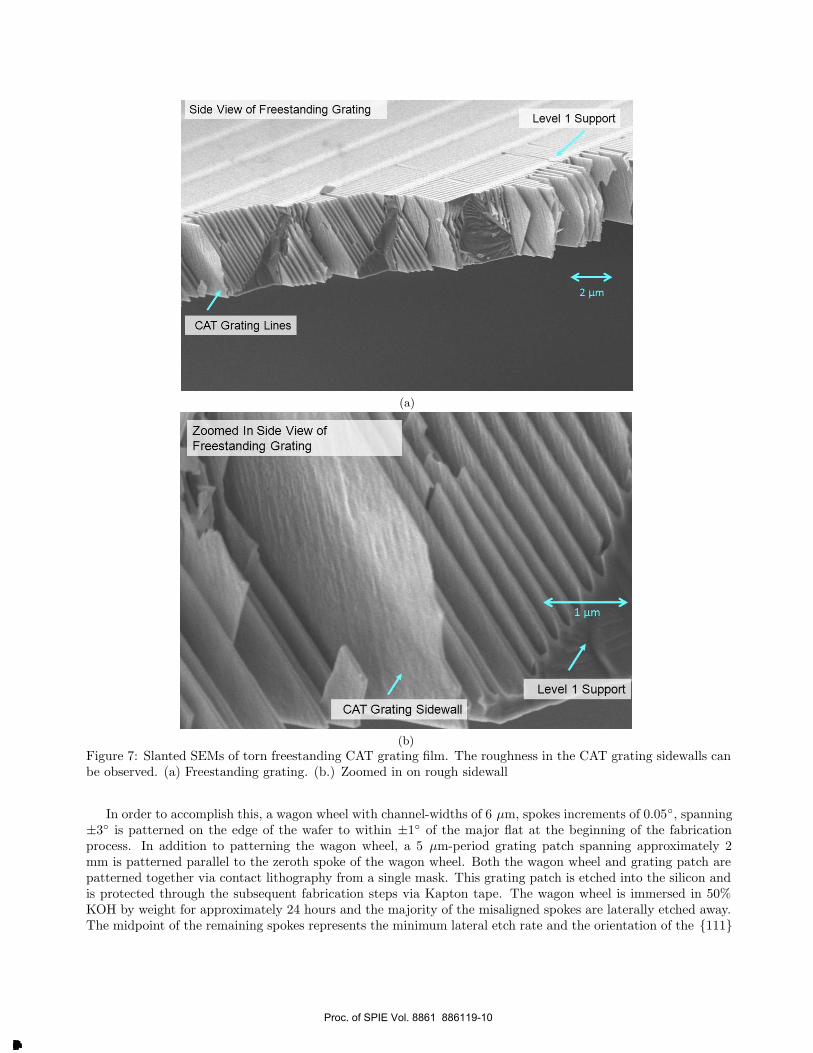
The process for a freestanding grating left sidewall roughness of approximately 4 nm RMS as measured with anAFM. The roughness was caused by both roughness in the Bosch DRIE step and line-edge roughness in the mask.In order to reduce the roughness, the grating was polished via KOH to reduce the sidewall roughness. See Figure7 for an SEM image showing the roughness on the sidewall of a freestanding grating. The polishing process isvery delicate and more details can be found by Bruccoleri et al.2,3 The key idea for KOH polishing is to start witha <110> wafer and align the grating bars to the {111} planes. KOH etches the non-{111} planes approximately100 times faster than the {111} planes,21 which means the grating can be etched to remove roughness for longdurations without destroying the structure. This requires precise (0.2◦) alignment to the {111} planes.
Proc. of SPIE Vol. 8861 886119-9
Downloaded From: http://proceedings.spiedigitallibrary.org/ on 10/17/2013 Terms of Use: http://spiedl.org/terms
Zoomed In Side View ofFreestanding Grating
Level 1 Support
CAT Grating Sidewall
Side View of Freestanding Grating
CAT Grating Lines
(a)
(b)
Figure 7: Slanted SEMs of torn freestanding CAT grating film. The roughness in the CAT grating sidewalls canbe observed. (a) Freestanding grating. (b.) Zoomed in on rough sidewall
In order to accomplish this, a wagon wheel with channel-widths of 6 μm, spokes increments of 0.05◦, spanning±3◦ is patterned on the edge of the wafer to within ±1◦ of the major flat at the beginning of the fabricationprocess. In addition to patterning the wagon wheel, a 5 μm-period grating patch spanning approximately 2mm is patterned parallel to the zeroth spoke of the wagon wheel. Both the wagon wheel and grating patch arepatterned together via contact lithography from a single mask. This grating patch is etched into the silicon andis protected through the subsequent fabrication steps via Kapton tape. The wagon wheel is immersed in 50%KOH by weight for approximately 24 hours and the majority of the misaligned spokes are laterally etched away.The midpoint of the remaining spokes represents the minimum lateral etch rate and the orientation of the {111}
Proc. of SPIE Vol. 8861 886119-10
Downloaded From: http://proceedings.spiedigitallibrary.org/ on 10/17/2013 Terms of Use: http://spiedl.org/terms
planes relative to the grating patch lines. An array of diffraction orders is created via this grating patch, fromeach arm of the Mach-Zehnder interference lithography table used to pattern the 200 nm-period CAT gratinglines.19 The array of diffraction orders from the 5 μm-period grating patch rotate as the wafer is rotated, andwhen the two arrays are parallel, the two incident arms of the Mach-Zehnder are at the same angle relative tothe grating patch lines. The 200 nm-period standing waves (image grating) are now parallel to the grating patchlines. Finally, the wafer can be rotated on a vernier chuck by the amount determined via the KOH etch of thewagon wheel, to align the 200 nm-period image grating to the {111} planes. The 200 nm-pitch CAT gratinglines are then exposed and developed.
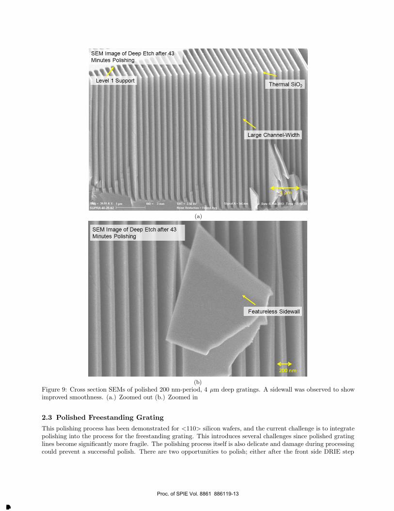
The CAT grating pattern is transferred into the mask and then deep-etched into silicon. An improved frontside process was created to increase the minimum bar-width. This was necessary since prior deep etches hada mininum bar width of approximately 50 nm and insufficient silicon remained between two {111} planes toenable successful polishing. See Figure 8 for SEM images of the improved DRIE process. The samples undergoa four-step clean after DRIE: piranha to remove the majority of the organic contamination, CR-7 to removechrome (if chrome is used in the masking process), ∼ 100 ml 3M Novec 7200 (C4F9OC2H5,)22 on a hot plate setfor 200◦ C for 10 minutes to remove the Bosch process polymer and 50:1 DI water:HF for 60 seconds to removenative SiO2. Following the clean step, the samples are polished in 50% KOH by weight at room temperatureand rinsed in DI water for times ranging between 20 and 43 minutes. The grating is fragile after polishing and itmust be critical-point dried to avoid damage from liquid-air surface tension forces. See Figure 9 for SEM imagesof the polished grating in bulk <110> silicon.
Proc. of SPIE Vol. 8861 886119-11
Downloaded From: http://proceedings.spiedigitallibrary.org/ on 10/17/2013 Terms of Use: http://spiedl.org/terms

SEM Image of ImprovedDeep Etch Sidewalls Thermal Si02
ma
Thermal SiO2
SEM Ige oImproved Deefp -Etch
h
Bulk Silicon
(a)
(b)
Figure 8: Cross section SEMs of the improved deep-etch process. This sample was etched for 9 minutes 30seconds and was not used for later polishing experiments. A sidewall was observed to show roughness. (a.)Zoomed out (b.) Zoomed in sidewall
Proc. of SPIE Vol. 8861 886119-12
Downloaded From: http://proceedings.spiedigitallibrary.org/ on 10/17/2013 Terms of Use: http://spiedl.org/terms
SEM Image of Deep Etch after 43IVIIf1l.ILes rUllsfllflC,J.
Featureless Sidewall
SEM Image of Deep Etch after 43Minutes Polishing
ww,ANNLevel 1 Support
Meg = 39 91 K X 1 pm i WD = 3 mm ENT = 2.50 kVSUPRA 40 -25 -92 I 7 Noise Reduction = F ' nie Avg
>
Thermal Sí02
Large Channel -Width
a Date :5 b 13 Time :17:19:30
(a)
(b)
Figure 9: Cross section SEMs of polished 200 nm-period, 4 μm deep gratings. A sidewall was observed to showimproved smoothness. (a.) Zoomed out (b.) Zoomed in
2.3 Polished Freestanding Grating
This polishing process has been demonstrated for <110> silicon wafers, and the current challenge is to integratepolishing into the process for the freestanding grating. This introduces several challenges since polished gratinglines become significantly more fragile. The polishing process itself is also delicate and damage during processingcould prevent a successful polish. There are two opportunities to polish; either after the front side DRIE step
Proc. of SPIE Vol. 8861 886119-13
Downloaded From: http://proceedings.spiedigitallibrary.org/ on 10/17/2013 Terms of Use: http://spiedl.org/terms

prior to filling and protecting (after step 3 in Figure 2) or at the end of the process after the back side DRIE. Ifpolishing occurs at the end of the process, the buried SiO2 would be removed after polishing instead of at step6, to avoid KOH from etching the grating bars from the bottom.
The experimental work has focused on polishing after DRIE and a freestanding grating has successfully beenfabricated; however, the tops of the grating bars are bent requiring further process refinement. The sample wascleaned and polished after DRIE for 30 minutes. It was then filled and protected with photoresist and carriedthrough the process outlined for a freestanding grating. The grating film survived the process unfortunately thetops of the grating bars were bent and often stuck together. See Figure 10 for SEM images of the freestandingpolished grating. They were thin at the top, less than 30 nm, and approximately 100 nm at the bottom whichsuggest the KOH etched the top faster than the bottom. It is also possible the sample was exposed to an air-liquid interface during processing and surface tension damaged the grating bars. Further experiments will becarried out to isolate the cause of the damage. A gentler filling step may be required as well to prevent damageto the grating bars which are twice as thin post polishing.
Proc. of SPIE Vol. 8861 886119-14
Downloaded From: http://proceedings.spiedigitallibrary.org/ on 10/17/2013 Terms of Use: http://spiedl.org/terms

Side View of Polished Freestanding GratingLevel 1 Support
CAT Grating Bars
Zoomed out Side View of PolishedFreestanding Grating
Level 1 Support
(a)
(b)
Figure 10
Proc. of SPIE Vol. 8861 886119-15
Downloaded From: http://proceedings.spiedigitallibrary.org/ on 10/17/2013 Terms of Use: http://spiedl.org/terms

Bottom Up View of PolishedFreestanding Grating
CAT Grating Lines
Level 1 Support
Top Down View of Polished MINFreestanding Grating _
IMM15000111""mgliw
mirar-Gating Lines
Level 1 Suppo'mo,..,..,
(c)
(d)
Figure 10: SEMs of freestanding polished CAT grating. (a.) and (b.) Zoomed out and zoomed in, slanted imagesof torn freestanding CAT grating film. (c.) Top down image of grating film. (d.) Bottom up image of gratingfilm.
3. CONCLUSION
Multiple nanofabrication processes are presented to create a CAT grating capable of undergoing testing withx-ray sources to demonstrate resolution and diffraction efficiency. The first process created a freestanding gratingwith unpolished sidewalls, a structure capable of undergoing structural tests. A successful process for polishingCAT grating bars in bulk <110> silicon via KOH is also presented. A combination of those two processes hasbeen presented to fabricate polished freestanding CAT gratings. The process is still in refinement as the gratingbars are too thin and bent at the top when the process is completed. Future experiments will be conducted to
Proc. of SPIE Vol. 8861 886119-16
Downloaded From: http://proceedings.spiedigitallibrary.org/ on 10/17/2013 Terms of Use: http://spiedl.org/terms
improve the understanding of the combined polishing and filling process. Modifications will be made to reducedamage to the grating bars and improve structural rigidity for the subsequent fabrication steps. Furthermorepolishing after the back side DRIE step will be explored if the filling process cannot be modified to preventdamaging the grating.
ACKNOWLEDGMENTS
This work was funded by NASA grants NNX11AF30G and NNX12AF21G, the MIT Kavli Institute and theDepartment of Defense National Defense Science and Engineering Graduate (NDSEG) fellowship program. Spe-cific thanks to James Daley of the MIT Nanostructures Lab, Vicky Diadiuk, Dennis Ward, Dave Terry and PaulTierney of the Microsystems Technology Laboratories, and Brian VanDerElzen of the University of MichiganLurie Nanofabrication Facility.
REFERENCES
[1] Bruccoleri, A., Mukherjee, P., Heilmann, R. K., Yam, J., Schattenburg, M. L., and DiPiazza, F., “Fabricationof nanoscale, high throughput, high aspect ratio freestanding gratings,” Journal of Vacuum Science &Technology B: Microelectronics and Nanometer Structures 30(6), 06FF03–06FF03–5 (2012).
[2] Bruccoleri, A., Fabrication of High-Throughput Critical-Angle X-ray Transmission Gratings for Wavelength-Dispersive Spectroscopy, doctoral thesis, Massachusetts Institute of Technology, Department of Aeronauticsand Astronautics (June 2013).
[3] Bruccoleri, A., Guan, D., Mukherjee, P., Heilmann, R. K., Vargo, S., and Schattenburg, M. L., “Potassiumhydroxide polishing of nanoscale deep reactive-ion etched ultra-high aspect ratio gratings,” Accepted forpublication in Journal of Vacuum Science & Technology B: Microelectronics and Nanometer Structures(2013).
[4] Heilmann, R. K., Davis, J. E., Dewey, D., Bautz, M. W., Foster, R., Bruccoleri, A., Mukherjee, P., Robin-son, D., Huenemoerder, D. P., Marshall, H. L., Schattenburg, M. L., Schulz, N. S., Guo, L. J., Kaplan,A. F., and Schweikart, R. B., “Critical-angle transmission grating spectrometer for high-resolution softx-ray spectroscopy on the International X-ray Observatory,” in [Proc. SPIE ], 7732, 77321J (July 2010).
[5] van Beek, J. T. M., Fleming, R. C., Hindle, P. S., Prentiss, J. D., Schattenburg, M. L., and Ritzau, S.,“Nanoscale freestanding gratings for ultraviolet blocking filters,” Journal of Vacuum Science & TechnologyB: Microelectronics and Nanometer Structures 16, 3911–3916 (Nov. 1998).
[6] David, C., Bruder, J., Rohbeck, T., Grunzweig, C., Kottler, C., Diaz, A., Bunk, O., and Pfeiffer, F., “Fab-rication of diffraction gratings for hard x-ray phase contrast imaging,” Microelectronic Engineering 84(5-8),1172–1177 (2007).
[7] Keith, D. W., Schattenburg, M. L., Smith, H. I., and Pritchard, D. E., “Diffraction of atoms by a transmis-sion grating,” Physical Review Letters 61, 1580–1583 (Oct 1988).
[8] Canizares, C. R., Schattenburg, M. L., and Smith, H. I., “The high energy transmission grating spectrometerfor AXAF,” in [Proc. SPIE ], 597, 253–260 (1986).
[9] Paerels, F., “X-ray diffraction gratings for astrophysics,” Space Science Reviews 157(1-4), 15–24 (2010).[10] Heilmann, R. K., Ahn, M., and Schattenburg, M. L., “Fabrication and performance of blazed transmis-
sion gratings for x-ray astronomy,” in [Society of Photo-Optical Instrumentation Engineers (SPIE) Confer-ence Series ], Society of Photo-Optical Instrumentation Engineers (SPIE) Conference Series 7011, 701106–701106–10 (Aug. 2008).
[11] Spiller, E., [Soft X-ray optics ], SPIE Optical Engineering Press, Bellingham, WA, (1994).[12] Bookbinder, J. A., Smith, R. K., Bandler, S., Garcia, M., Hornschemeier, A., Petre, R., and Ptak, A., “The
Advanced X-ray Spectroscopic Imaging Observatory (AXSIO),” in [Society of Photo-Optical Instrumen-tation Engineers (SPIE) Conference Series ], Society of Photo-Optical Instrumentation Engineers (SPIE)Conference Series 8443, 844317–844317–7 (Sept. 2012).
Proc. of SPIE Vol. 8861 886119-17
Downloaded From: http://proceedings.spiedigitallibrary.org/ on 10/17/2013 Terms of Use: http://spiedl.org/terms

[13] Vikhlinin, A., Reid, P., Tananbaum, H., Schwartz, D. A., Forman, W. R., Jones, C., Bookbinder, J.,Cotroneo, V., Trolier-McKinstry, S., Burrows, D., Bautz, M. W., Heilmann, R., Davis, J., Bandler, S. R.,Weisskopf, M. C., and Murray, S. S., “SMART-X: Square Meter Arcsecond Resolution x-ray Telescope,” in[Society of Photo-Optical Instrumentation Engineers (SPIE) Conference Series ], Society of Photo-OpticalInstrumentation Engineers (SPIE) Conference Series 8443, 844316–844316–11 (Sept. 2012).
[14] Mukherjee, P., Zurbuchen, T. H., and Jay Guo, L., “Fabrication and testing of freestanding Si nanogratingsfor UV filtration on space-based particle sensors,” Nanotechnology 20, 325301 (Aug. 2009).
[15] Kovacs, G. T. A., Maluf, N. I., and Petersen, K. E., “Bulk micromachining of silicon,” Proc. IEEE 86(8),1536–1551 (1998).
[16] Jeong, D.-H., Yun, S.-S., Lee, M.-L., Hwang, G., Choi, C.-A., and Lee, J.-H., “Novel micro capacitive incli-nometer with oblique comb electrode and suspension spring aligned parallel to {111} vertical planes of (110)silicon,” in [Micro Electro Mechanical Systems, 2009. MEMS 2009. IEEE 22nd International Conferenceon ], 797–800 (Jan.).
[17] Jeong, D.-H., Yun, S.-S., Lee, B.-G., Lee, M.-L., Choi, C.-A., and Lee, J.-H., “High-resolution capacitive mi-croinclinometer with oblique comb electrodes using (110) silicon,” Microelectromechanical Systems, Journalof 20(6), 1269–1276 (Dec.).
[18] Mukherjee, P., Bruccoleri, A., Heilmann, R. K., Schattenburg, M. L., Kaplan, A., and Guo, L., “Plasmaetch fabrication of 60:1 aspect ratio silicon nanogratings with 200 nm pitch,” Journal of Vacuum Science &Technology B: Microelectronics and Nanometer Structures 28(6), C6P70–C6P75 (2010).
[19] Schattenburg, M. L., Anderson, E. H., and Smith, H. I., “X-ray/VUV transmission gratings for astrophysicaland laboratory applications,” Physica Scripta 41, 13–20 (Jan. 1990).
[20] Schattenburg, M. L., “From nanometers to gigaparsecs: The role of nanostructures in unraveling the mys-teries of the cosmos,” Journal of Vacuum Science & Technology B: Microelectronics and Nanometer Struc-tures 19, 2319–2328 (Nov. 2001).
[21] Ahn, M., Fabrication of critical-angle transmission gratings for high efficiency x-ray spectroscopy , doctoralthesis, Massachusetts Institute of Technology, Department of Mechanical Engineering (February 2009).
[22] Clark, P. G., Olson, E. D., and Kofuse, H., “The Use of Segregated Hydrofluoroethers as Cleaning Agentsin Electronic Packaging Applications,” International Conference on Soldering and Reliability, Toronto, On-tario, Canada (May 2009).
Proc. of SPIE Vol. 8861 886119-18
Downloaded From: http://proceedings.spiedigitallibrary.org/ on 10/17/2013 Terms of Use: http://spiedl.org/terms