Embed Size (px)
Citation preview
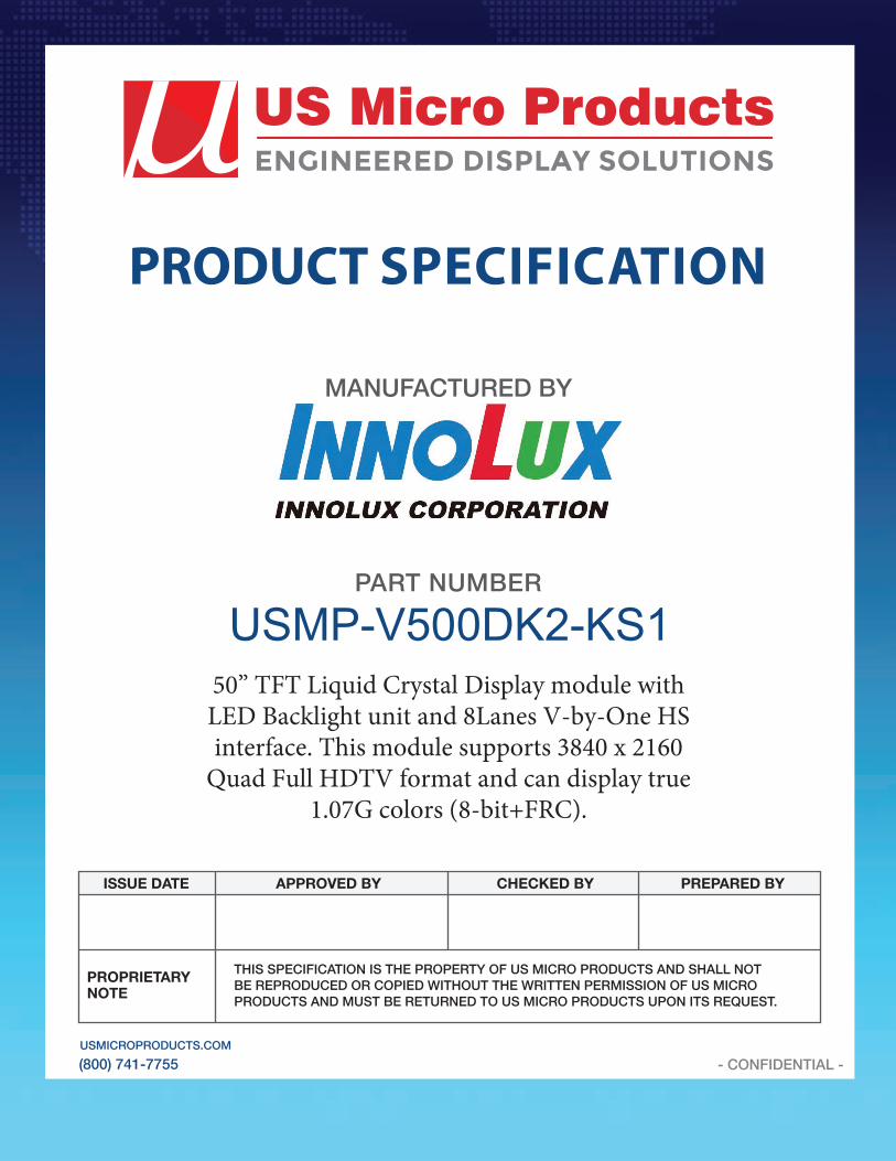
PRODUCT SPECIFICATION
MANUFACTURED BY
PART NUMBER
ISSUE DATE APPROVED BY CHECKED BY PREPARED BY
PROPRIETARYNOTE
THIS SPECIFICATION IS THE PROPERTY OF US MICRO PRODUCTS AND SHALL NOTBE REPRODUCED OR COPIED WITHOUT THE WRITTEN PERMISSION OF US MICROPRODUCTS AND MUST BE RETURNED TO US MICRO PRODUCTS UPON ITS REQUEST.
USMICROPRODUCTS.COM
(800) 741-7755 - CONFIDENTIAL -
USMP-V500DK2-KS150” TFT Liquid Crystal Display module with LED Backlight unit and 8Lanes V-by-One HS interface. This module supports 3840 x 2160
Quad Full HDTV format and can display true 1.07G colors (8-bit+FRC).

PRODUCT SPECIFICATION
Version 2.0 1 Date : Sep.24 2013
The copyright belongs to InnoLux. Any unauthorized use is prohibited
Tentative Specification
Preliminary Specification
Approval Specification
MODEL NO.: V500DK2
SUFFIX: KS1
Revision : C8
Customer :
APPROVED BY SIGNATURE
Name / Title
Note
Please return 1 copy for your confirmation with your signature and comments.
Approved By Checked By Prepared By
Chao-Chun Chung
Carlos Lee
WT Hsu
WWW.USMICROPRODUCTS.COM (800) 741-7755
CO
NFI
DE
NTI
AL
PRODUCT SPECIFICATION
Version 2.0 2 Date : Sep.24 2013
The copyright belongs to InnoLux. Any unauthorized use is prohibited
CONTENTS
CONTENTS .......................................................................................................................................................................2
REVISION HISTORY ........................................................................................................................................................4
Modify GENERAL SPECIFICATIONS.................................................................................................................................. 4
Modify MECHANICAL CHARACTERISTIC ...................................................................................................................4
1. GENERAL DESCRIPTION ............................................................................................................................................5
1.1 OVERVIEW ......................................................................................................................................................................... 5
1.2 FEATURES .......................................................................................................................................................................... 5
1.3 GENERAL SPECIFICATIONS.......................................................................................................................................... 5
1.4 MECHANICAL SPECIFICATIONS................................................................................................................................. 6
2. ABSOLUTE MAXIMUM RATINGS ..............................................................................................................................7
2.1 ABSOLUTE RATINGS OF ENVIRONMENT................................................................................................................. 7
2.2 PACKAGE STORAGE ....................................................................................................................................................... 8
2.3 ELECTRICAL ABSOLUTE RATINGS............................................................................................................................. 8
2.3.1 TFT LCD MODULE......................................................................................................................................................... 8
2.3.2 BACKLIGHT CONVERTER UNIT ............................................................................................................................... 8
3. ELECTRICAL CHARACTERISTICS..............................................................................................................................9
3.1 TFT LCD MODULE............................................................................................................................................................ 9
3.2 BACKLIGHT UNIT.......................................................................................................................................................... 12
3.2.1 CONVERTER CHARACTERISTICS........................................................................................................................... 12
3.2.2 CONVERTER INTERFACE CHARACTERISTICS ................................................................................................... 14
4. BLOCK DIAGRAM OF INTERFACE ..........................................................................................................................16
4.1 TFT LCD MODULE.......................................................................................................................................................... 16
5 .INPUT TERMINAL PIN ASSIGNMENT.....................................................................................................................17
5.1 TFT LCD MODULE.......................................................................................................................................................... 17
5.2 BACKLIGHT UNIT.......................................................................................................................................................... 21
5.3 CONVERTER UNIT......................................................................................................................................................... 22
5.4 COLOR DATA INPUT ASSIGNMENT......................................................................................................................... 24
6. INTERFACE TIMING..................................................................................................................................................25
6.1 INPUT SIGNAL TIMING SPECIFICATIONS .............................................................................................................. 25
WWW.USMICROPRODUCTS.COM (800) 741-7755
CO
NFI
DE
NTI
AL

PRODUCT SPECIFICATION
Version 2.0 3 Date : Sep.24 2013
The copyright belongs to InnoLux. Any unauthorized use is prohibited
6.1. 1 Timing spec for QFHD Frame Rate = 50Hz .................................................................................................... 25
6.1. 2 Timing spec for QFHD Frame Rate = 60Hz .................................................................................................... 25
6.1.3 Input Timing Spec for FHD, Frame Rate = 50Hz............................................................................................ 26
6.1.4 Input Timing Spec for FHD, Frame Rate = 60Hz............................................................................................ 26
6.1.5 Input Timing Spec for FHD, Frame Rate = 100Hz.......................................................................................... 27
6.1.6 Input Timing Spec for FHD, Frame Rate = 120Hz.......................................................................................... 27
6.1.7 Input Timing spec for QFHD, Frame Rate = 24Hz......................................................................................... 28
6.1.8 Input Timing spec for QFHD, Frame Rate = 30Hz......................................................................................... 28
6.2 V by One Input Signal Timing Diagram ....................................................................................................................... 31
6.3 Byte Length and Color mapping of V-by-One HS....................................................................................................... 31
6.4 POWER ON/OFF SEQUENCE ...................................................................................................................................... 33
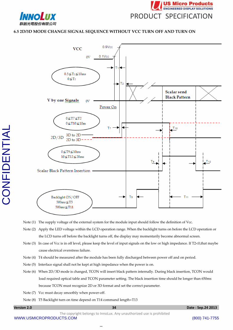
6.5 2D/3D MODE CHANGE SIGNAL SEQUENCE WITHOUT VCC TURN OFF AND TURN ON........................ 34
7. OPTICAL CHARACTERISTICS ..................................................................................................................................35
7.1 TEST CONDITIONS ........................................................................................................................................................ 35
7.2 OPTICAL SPECIFICATIONS ......................................................................................................................................... 36
8. PRECAUTIONS ...........................................................................................................................................................41
8.1 ASSEMBLY AND HANDLING PRECAUTIONS........................................................................................................ 41
8.2 SAFETY PRECAUTIONS ................................................................................................................................................ 41
8.3 SAFETY STANDARDS.................................................................................................................................................... 41
9. DEFINITION OF LABELS ...........................................................................................................................................42
9.1 MODULE LABEL ............................................................................................................................................................. 42
9.2 CARTON LABEL.............................................................................................................................................................. 43
10. PACKAGING.............................................................................................................................................................44
10.1 PACKAGING SPECIFICATIONS ................................................................................................................................ 44
10.2 PACKAGING METHOD............................................................................................................................................... 44
10.3 UN-PACKAGING METHOD....................................................................................................................................... 45
11. MECHANICAL CHARACTERISTIC ........................................................................................................................46
WWW.USMICROPRODUCTS.COM (800) 741-7755
CO
NFI
DE
NTI
AL

PRODUCT SPECIFICATION
Version 2.0 4 Date : Sep.24 2013
The copyright belongs to InnoLux. Any unauthorized use is prohibited
REVISION HISTORY
Version Date Page
(New) Section Description
0.0
1.0
2.0
Aug.1.2013
Aug.21.2013
Sep.24.2013
All
16
17
25
25
26
26
26-27
27
27-28
28
36
44-45
45
5
8
12
16
17-19
25-28
33
34
45
43
All
4.1
5.1
6.1.1
6.1.2
6.1.3
6.1.4
6.1.5
6.1.6
6.1.7
6.1.8
7.2
10.2
10.3
1.3
3.1
3.2.1
4.1
5.1
6.1
6.4
6.5
11
10.1
Tentative Specification Ver 0.0 was first issued.
Modify TFT LCD MODULE
Modify TFT LCD MODULE
Modify Timing spec for QFHD Frame Rate = 50Hz
Modify Timing spec for QFHD Frame Rate = 60Hz
Modify Input Timing Spec for FHD, Frame Rate = 50Hz
Modify Input Timing Spec for FHD, Frame Rate = 60Hz
Modify Input Timing Spec for FHD, Frame Rate = 100Hz
Modify Input Timing Spec for FHD, Frame Rate = 120Hz
Modify Input Timing spec for QFHD, Frame Rate = 24Hz
Modify Input Timing spec for QFHD, Frame Rate = 30Hz
Modify OPTICAL SPECIFICATIONS
Modify PACKAGING METHOD
Modify UN-PACKAGING METHOD
Modify GENERAL SPECIFICATIONS
Modify TFT LCD MODULE
Modify CONVERTER CHARACTERISTICS
Modify TFT LCD MODULE
Modify TFT LCD MODULE
Modify INPUT SIGNAL TIMING SPECIFICATIONS
Modify POWER ON/OFF SEQUENCE
Modify 2D/3D MODE CHANGE SIGNAL SEQUENCE
WITHOUT VCC TURN OFF AND TURN ON
Modify MECHANICAL CHARACTERISTIC
Modify PACKAGING SPECIFICATIONS
WWW.USMICROPRODUCTS.COM (800) 741-7755
CO
NFI
DE
NTI
AL
PRODUCT SPECIFICATION
Version 2.0 5 Date : Sep.24 2013
The copyright belongs to InnoLux. Any unauthorized use is prohibited
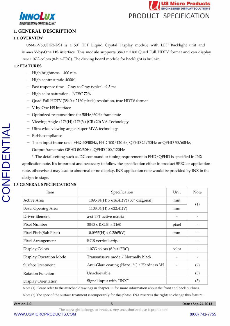
1. GENERAL DESCRIPTION
1.1 OVERVIEW
USMP-V500DK2-KS1 is a 50” TFT Liquid Crystal Display module with LED Backlight unit and
8Lanes V-by-One HS interface. This module supports 3840 x 2160 Quad Full HDTV format and can display
true 1.07G colors (8-bit+FRC). The driving board module for backlight is built-in.
1.2 FEATURES
- High brightness 400 nits
- High contrast ratio 4000:1
- Fast response time Gray to Gray typical : 9.5 ms
- High color saturation NTSC 72%
- Quad Full HDTV (3840 x 2160 pixels) resolution, true HDTV format
- V-by-One HS interface
- Optimized response time for 50Hz/60Hz frame rate
- Viewing Angle : 176(H)/176(V) (CR>20) VA Technology
- Ultra wide viewing angle: Super MVA technology
- RoHs compliance
- T-con input frame rate : FHD 50/60Hz, FHD 100/120Hz, QFHD 24/30Hz or QFHD 50/60Hz,
Output frame rate: QFHD 50/60Hz, QFHD 100/120Hz
*: The detail setting such as I2C command or timing requirement in FHD/QFHD is specified in INX
application note. It’s important and necessary to follow the specification either in product SPEC or application
note, otherwise it may lead to abnormal or no display. INX application note would be provided by INX in the
design-in stage.
1.3 GENERAL SPECIFICATIONS
Item Specification Unit Note
Active Area 1095.84(H) x 616.41(V) (50” diagonal) mm
Bezel Opening Area 1103.04(H) x 622.41(V) mm (1)
Driver Element a-si TFT active matrix - -
Pixel Number 3840 x R.G.B. x 2160 pixel -
Pixel Pitch(Sub Pixel) 0.0955(H) x 0.2865(V) mm -
Pixel Arrangement RGB vertical stripe - -
Display Colors 1.07G colors (8-bit+FRC) color -
Display Operation Mode Transmissive mode / Normally black - -
Surface Treatment Anti-Glare coating (Haze 1%),Hardness 3H - (2)
Rotation Function Unachievable (3)
Display Orientation Signal input with “INX” (3)
Note (1) Please refer to the attached drawings in chapter 11 for more information about the front and back outlines.
Note (2) The spec of the surface treatment is temporarily for this phase. INX reserves the rights to change this feature.
WWW.USMICROPRODUCTS.COM (800) 741-7755
CO
NFI
DE
NTI
AL

PRODUCT SPECIFICATION
Version 2.0 6 Date : Sep.24 2013
The copyright belongs to InnoLux. Any unauthorized use is prohibited
Note (3)
1.4 MECHANICAL SPECIFICATIONS
Item Min. Typ. Max. Unit Note
Horizontal (H) 1113.84 1115.04 1116.24 mm (1),(2)
Vertical (V) 637.21 638.41 639.61 mm (1),(2)
15.2 16.2 17.2 mm To Rear
Module Size
Depth (D) 26.6 27.6 28.6 mm
To converter cover
Weight 11144 11730 12316 g
Note (1) Please refer to the attached drawings for more information of front and back outline dimensions.
Note (2) Module Depth does not include connectors.
Back Side
Tcon Board
Front Side
INX
WWW.USMICROPRODUCTS.COM (800) 741-7755
CO
NFI
DE
NTI
AL

PRODUCT SPECIFICATION
Version 2.0 7 Date : Sep.24 2013
The copyright belongs to InnoLux. Any unauthorized use is prohibited
2. ABSOLUTE MAXIMUM RATINGS
2.1 ABSOLUTE RATINGS OF ENVIRONMENT
Value Item Symbol
Min. Max. Unit Note
Storage Temperature TST -20 +60 ºC (1)
Operating Ambient Temperature TOP 0 50 ºC (1), (2)
Shock (Non-Operating) SNOP - 35 G (3), (5)
Vibration (Non-Operating) VNOP - 1.0 G (4), (5)
Note (1) Temperature and relative humidity range is shown in the figure below.
(a) 90 %RH Max. (Ta 40 ºC).≦
(b) Wet-bulb temperature should be 39 ºC Max. (Ta > 40 ºC).
(c) No condensation.
Note (2) Thermal management should be considered in final product design to prevent the surface temperature of display
area from being over 65 ºC. The range of operating temperature may degrade in case of improper thermal
management in final product design.
Note (3) 11 ms, half sine wave, 1 time for ± X, ± Y, ± Z.
Note (4) 10 ~ 200 Hz, 30 min, 1 time each X, Y, Z.
Note (5) At testing Vibration and Shock, the fixture in holding the module has to be hard and rigid enough so that the
module would not be twisted or bent by the fixture.
Relative Humidity (%RH)
Operating Range
Temperature (ºC)
100
80 60 -20 40 0 20 -40
90
80
40
60
20
10 Storage Range
WWW.USMICROPRODUCTS.COM (800) 741-7755
CO
NFI
DE
NTI
AL
PRODUCT SPECIFICATION
Version 2.0 8 Date : Sep.24 2013
The copyright belongs to InnoLux. Any unauthorized use is prohibited
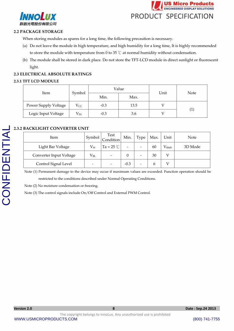
2.2 PACKAGE STORAGE
When storing modules as spares for a long time, the following precaution is necessary.
(a) Do not leave the module in high temperature, and high humidity for a long time, It is highly recommended
to store the module with temperature from 0 to 35 at normal humidity without condensation.
(b) The module shall be stored in dark place. Do not store the TFT-LCD module in direct sunlight or fluorescent
light.
2.3 ELECTRICAL ABSOLUTE RATINGS
2.3.1 TFT LCD MODULE
Value Item Symbol
Min. Max. Unit Note
Power Supply Voltage VCC -0.3 13.5 V
Logic Input Voltage VIN -0.3 3.6 V (1)
2.3.2 BACKLIGHT CONVERTER UNIT
Item Symbol Test
Condition Min. Type Max. Unit Note
Light Bar Voltage VW Ta = 25 - - 60 VRMS 3D Mode
Converter Input Voltage VBL - 0 - 30 V
Control Signal Level - - -0.3 - 6 V
Note (1) Permanent damage to the device may occur if maximum values are exceeded. Function operation should be
restricted to the conditions described under Normal Operating Conditions.
Note (2) No moisture condensation or freezing.
Note (3) The control signals include On/Off Control and External PWM Control.
WWW.USMICROPRODUCTS.COM (800) 741-7755
CO
NFI
DE
NTI
AL

PRODUCT SPECIFICATION
Version 2.0 9 Date : Sep.24 2013
The copyright belongs to InnoLux. Any unauthorized use is prohibited
3. ELECTRICAL CHARACTERISTICS
3.1 TFT LCD MODULE
(Ta = 25 ± 2 ºC)
Value Parameter Symbol
Min. Typ. Max.
Unit Note
Power Supply Voltage VCC 10.8 12 13.2 V (1)
Rush Current IRUSH - - 3.4 A (2)
White Pattern PT - 17.28 20.76 W
Horizontal Stripe PT - 25.68 31.2 W OFHD 120Hz Output
Power Consumption
Black Pattern PT - 17.16 20.64 W
White Pattern - - 1.44 1.73 A
Horizontal Stripe - - 2.14 2.6 A OFHD 120Hz Output
Power Supply Current
Black Pattern - - 1.43 1.72 A
White Pattern PT - 12.24 14.88 W
Horizontal Stripe PT - 26.52 31.68 W QFHD 60Hz Output
Power Consumption
Black Pattern PT - 12.36 15 W
White Pattern - - 1.02 1.24 A
Horizontal Stripe - - 2.21 2.64 A QFHD 60Hz Output
Power Supply Current
Black Pattern - - 1.03 1.25 A
(3)
Differential Input High
Threshold Voltage VLVTH - - +50 mV
Differential Input Low Threshold Voltage
VLVTL -50 - - mV V-by-One
HS Differential input voltage
(single-end) |VID| 200 - 600 mV
(4)
Input High Threshold Voltage VIH 2.7 - 3.6 V CMOS
interface Input Low Threshold Voltage VIL 0 - 0.7 V
WWW.USMICROPRODUCTS.COM (800) 741-7755
CO
NFI
DE
NTI
AL
PRODUCT SPECIFICATION
Version 2.0 10 Date : Sep.24 2013
The copyright belongs to InnoLux. Any unauthorized use is prohibited
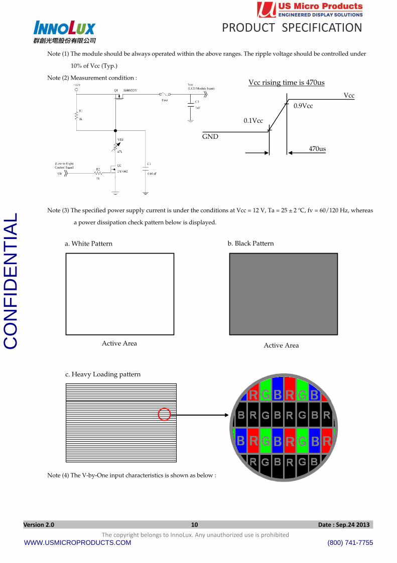
Note (1) The module should be always operated within the above ranges. The ripple voltage should be controlled under
10% of Vcc (Typ.)
Note (2) Measurement condition :
Note (3) The specified power supply current is under the conditions at Vcc = 12 V, Ta = 25 ± 2 ºC, fv = 60/120 Hz, whereas
a power dissipation check pattern below is displayed.
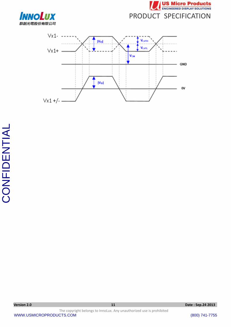
Note (4) The V-by-One input characteristics is shown as below :
Vcc rising time is 470us
470us
Vcc
GND
0.9Vcc
0.1Vcc
Active Area
b. Black Pattern
Active Area
a. White Pattern
c. Heavy Loading pattern
WWW.USMICROPRODUCTS.COM (800) 741-7755
CO
NFI
DE
NTI
AL
PRODUCT SPECIFICATION
Version 2.0 11 Date : Sep.24 2013
The copyright belongs to InnoLux. Any unauthorized use is prohibited
WWW.USMICROPRODUCTS.COM (800) 741-7755
CO
NFI
DE
NTI
AL
PRODUCT SPECIFICATION
Version 2.0 12 Date : Sep.24 2013
The copyright belongs to InnoLux. Any unauthorized use is prohibited
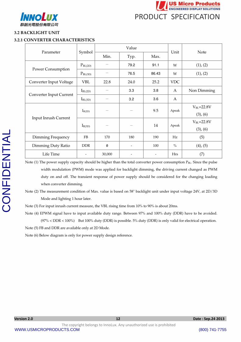
3.2 BACKLIGHT UNIT
3.2.1 CONVERTER CHARACTERISTICS
Value Parameter Symbol
Min. Typ. Max. Unit Note
PBL(2D) - 79.2 91.1 W (1), (2) Power Consumption
PBL(3D) - 76.5 86.43 W (1), (2)
Converter Input Voltage VBL 22.8 24.0 25.2 VDC
IBL(2D) - 3.3 3.8 A Non Dimming Converter Input Current
IBL(3D) - 3.2 3.6 A
IR(2D) - - 9.5 Apeak VBL=22.8V
(3), (6) Input Inrush Current
IR(3D) - - 14 Apeak VBL=22.8V
(3), (6)
Dimming Frequency FB 170 180 190 Hz (5)
Dimming Duty Ratio DDR 0 - 100 % (4), (5)
Life Time - 30,000 - - Hrs (7)
Note (1) The power supply capacity should be higher than the total converter power consumption PBL. Since the pulse
width modulation (PWM) mode was applied for backlight dimming, the driving current changed as PWM
duty on and off. The transient response of power supply should be considered for the changing loading
when converter dimming.
Note (2) The measurement condition of Max. value is based on 58" backlight unit under input voltage 24V, at 2D/3D
Mode and lighting 1 hour later.
Note (3) For input inrush current measure, the VBL rising time from 10% to 90% is about 20ms.
Note (4) EPWM signal have to input available duty range. Between 97% and 100% duty (DDR) have to be avoided.
(97% < DDR < 100%) But 100% duty (DDR) is possible. 5% duty (DDR) is only valid for electrical operation.
Note (5) FB and DDR are available only at 2D Mode.
Note (6) Below diagram is only for power supply design reference.
WWW.USMICROPRODUCTS.COM (800) 741-7755
CO
NFI
DE
NTI
AL

PRODUCT SPECIFICATION
Version 2.0 13 Date : Sep.24 2013
The copyright belongs to InnoLux. Any unauthorized use is prohibited
Note (7) The lifetime is defined as the time which luminance of the LED decays to 50% compared to the initial value,
Operating condition: Continuous operating at Ta = 25±2
WWW.USMICROPRODUCTS.COM (800) 741-7755
CO
NFI
DE
NTI
AL

PRODUCT SPECIFICATION
Version 2.0 14 Date : Sep.24 2013
The copyright belongs to InnoLux. Any unauthorized use is prohibited
3.2.2 CONVERTER INTERFACE CHARACTERISTICS
Value Parameter Symbol
Test
Condition Min. Typ. Max. Unit Note
ON - 2.0 - 5.0 V On/Off Control
Voltage OFF VBLON
- 0 - 0.8 V
HI - 2.0 - 5.25 V Duty on External PWM Control
Voltage LO
VEPWM
- 0 - 0.8 V Duty off (5), (6)
External PWM Frequency FEPWM - 150 160 170 Hz Normal mode (7)
Error Signal ERR - - - - - Abnormal: Open
VBL Rising Time Tr1 - 20 - - ms 10%-90%VBL
Control Signal Rising Time Tr - - - 100 ms
Control Signal Falling Time Tf - - - 100 ms
PWM Signal Rising Time TPWMR - - - 50 us
PWM Signal Falling Time TPWMF - - - 50 us (6)
Input Impedance Rin - 1 - - MΩ EPWM, BLON
PWM Delay Time TPWM - 100 - - ms (6)
Ton - 300 - - ms BLON Delay Time
Ton1 - 300 - - ms
BLON Off Time Toff - 300 - - ms
Note (1) The Dimming signal should be valid before backlight turns on by BLON signal. It is inhibited to change the
external PWM signal during backlight turn on period.
Note (2) The power sequence and control signal timing are shown in the Fig.1. For a certain reason, the converter has a
possibility to be damaged with wrong power sequence and control signal timing.
Note (3) While system is turned ON or OFF, the power sequences must follow as below descriptions:
Turn ON sequence: VBL → PWM signal → BLON
Turn OFF sequence: BLOFF → PWM signal → VBL
Note (4) When converter protective function is triggered, ERR will output open collector status. Please refers to Fig.2.
Note (5) The EPWM interface that inserts a pull up resistor to 5V in Max Duty (100%), please refers to Fig.3.
Note (6) EPWM is available only at 2D Mode.
Note (7) EPWM signal have to input available frequency range.
Note (8) [Recommend] EPWM duty ratio is set at 100%(Max. Brightness) in 3D Mode.
Note (9) Used the EPWM signal control user dimming only in 2D normal Mode. 2D scan and 2D local dimming Mode
please reference 5.1 Note (11) and application Note.
WWW.USMICROPRODUCTS.COM (800) 741-7755
CO
NFI
DE
NTI
AL

PRODUCT SPECIFICATION
Version 2.0 15 Date : Sep.24 2013
The copyright belongs to InnoLux. Any unauthorized use is prohibited
2.0V
0.8V
Tr TfBacklight on duration
0
VEPWM
VW
Ton
100%
ExternalPWM Duty
VBL
VBLON
0
0
2.0V
0.8V
Toff
ExternalPWMPeriod
Tr1
Ext. Dimming Function
TPWMF
TPWMR
TPWM
Floating
Ton1
0.9VBL
0.1VBL
Fig. 1
Fig. 2 Fig. 3
WWW.USMICROPRODUCTS.COM (800) 741-7755
CO
NFI
DE
NTI
AL

PRODUCT SPECIFICATION
Version 2.0 16 Date : Sep.24 2013
The copyright belongs to InnoLux. Any unauthorized use is prohibited
4. BLOCK DIAGRAM OF INTERFACE
4.1 TFT LCD MODULE
2D/3D L/R LD_EN VCC L/R_O GND SDA SCL
C Board
TFT LCD PANEL
(3840x3x2160)
XR Board XL Board
E_PWM
VBL
GND
ERR
BLON
CONVERTER CONNECTOR
CN1: CI0114M1HR0-LA
(CvilLux)
CN2: CI0105M1HR0-LA
(CvilLux))
LED
BACKLIGHT
UNIT
INPUT CONNECTOR
CNF1: 187059-51221(P-TWO)
RX0N RX0P RX1N RX1P RX2N RX2P RX3N RX3P
RX4N RX4P RX5N RX5P RX6N RX6P RX7N RX7P
WWW.USMICROPRODUCTS.COM (800) 741-7755
CO
NFI
DE
NTI
AL

PRODUCT SPECIFICATION
Version 2.0 17 Date : Sep.24 2013
The copyright belongs to InnoLux. Any unauthorized use is prohibited
5 .INPUT TERMINAL PIN ASSIGNMENT
5.1 TFT LCD MODULE
CNV1 Connector Pin Assignment (187059-51221(P-TWO))
Pin Name Description Note
1 Vin Power input (+12V)
2 Vin Power input (+12V)
3 Vin Power input (+12V)
4 Vin Power input (+12V)
5 Vin Power input (+12V)
6 Vin Power input (+12V)
7 Vin Power input (+12V)
8 Vin Power input (+12V)
9 N.C. No Connection (10)
10 GND Ground
11 GND Ground
12 GND Ground
13 GND Ground
14 GND Ground
15 L/R_O Output signal for Glasses Left Right signal, (5)
16 L/R Input signal for Left/Right synchronous signal. (3) (7)
17 2D/3D 2D/3D Enable (2) (7)
18 SDA I2C Data signal (11)(12)
19 SCL I2C Clock signal (11)(12)
20 N.C. No Connection
21 N.C. No Connection (10)
22 LD_EN Local Dimming Mode Enable. (4) (6)
23 N.C. No Connection (10)
24 N.C. No Connection (10)
25 HTPDN Hot plug detect output, Open drain.
26 LOCKN Lock detect output, Open drain.
27 GND Ground
28 RX0N 1ST Pixel Negative V-by-One differential data input in area A. Lane 0
29 RX0P 1ST Pixel Positive V-by-One differential data input in area A. Lane 0 (1)
30 GND Ground
31 RX1N 2ND Pixel Negative V-by-One differential data input in area A. Lane 1
32 RX1P
2ND Pixel Positive V-by-One differential data input in area A. Lane
1
(1)
33 GND Ground
WWW.USMICROPRODUCTS.COM (800) 741-7755
CO
NFI
DE
NTI
AL
PRODUCT SPECIFICATION
Version 2.0 18 Date : Sep.24 2013
The copyright belongs to InnoLux. Any unauthorized use is prohibited
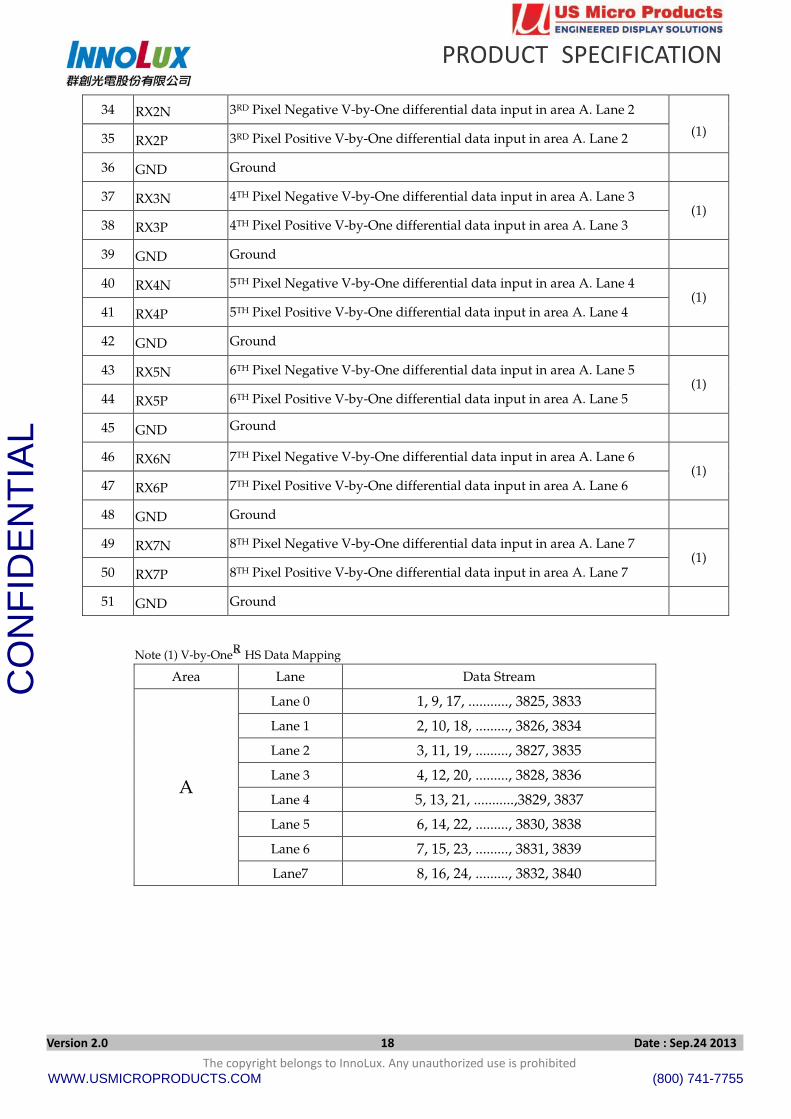
34 RX2N 3RD Pixel Negative V-by-One differential data input in area A. Lane 2
35 RX2P 3RD Pixel Positive V-by-One differential data input in area A. Lane 2
(1)
36 GND Ground
37 RX3N 4TH Pixel Negative V-by-One differential data input in area A. Lane 3
38 RX3P 4TH Pixel Positive V-by-One differential data input in area A. Lane 3 (1)
39 GND Ground
40 RX4N 5TH Pixel Negative V-by-One differential data input in area A. Lane 4
41 RX4P 5TH Pixel Positive V-by-One differential data input in area A. Lane 4 (1)
42 GND Ground
43 RX5N 6TH Pixel Negative V-by-One differential data input in area A. Lane 5
44 RX5P 6TH Pixel Positive V-by-One differential data input in area A. Lane 5 (1)
45 GND Ground
46 RX6N 7TH Pixel Negative V-by-One differential data input in area A. Lane 6
47 RX6P 7TH Pixel Positive V-by-One differential data input in area A. Lane 6 (1)
48 GND Ground
49 RX7N 8TH Pixel Negative V-by-One differential data input in area A. Lane 7
50 RX7P 8TH Pixel Positive V-by-One differential data input in area A. Lane 7 (1)
51 GND Ground
Note (1) V-by-OneR HS Data Mapping
Area Lane Data Stream
Lane 0 1, 9, 17, ..........., 3825, 3833
Lane 1 2, 10, 18, ........., 3826, 3834
Lane 2 3, 11, 19, ........., 3827, 3835
Lane 3 4, 12, 20, ........., 3828, 3836
Lane 4 5, 13, 21, ...........,3829, 3837
Lane 5 6, 14, 22, ........., 3830, 3838
Lane 6 7, 15, 23, ........., 3831, 3839
A
Lane7 8, 16, 24, ........., 3832, 3840
WWW.USMICROPRODUCTS.COM (800) 741-7755
CO
NFI
DE
NTI
AL

PRODUCT SPECIFICATION
Version 2.0 19 Date : Sep.24 2013
The copyright belongs to InnoLux. Any unauthorized use is prohibited
Note (2) 2D/3D mode selection.
L= Connect to GND or Open, H=Connect to +3.3V
2D/3D Note
L or Open 2D Mode
H 3D Mode
Note (3) Input signal for Left Right eye frame synchronous
VIL=0~0.8 V, VIH=2.0~3.3 V
L/R Note
L Right synchronous signal
H Left synchronous signal
Note (4) Local dimming enable selection. (Default: enable)
L= Connect to GND, H=Connect to +3.3V or Open
LD_EN Note
L Local Dimming Disable
H or Open Local Dimming Enable
LD_EN enable pin should be set in power on stage.
WWW.USMICROPRODUCTS.COM (800) 741-7755
CO
NFI
DE
NTI
AL
PRODUCT SPECIFICATION
Version 2.0 20 Date : Sep.24 2013
The copyright belongs to InnoLux. Any unauthorized use is prohibited
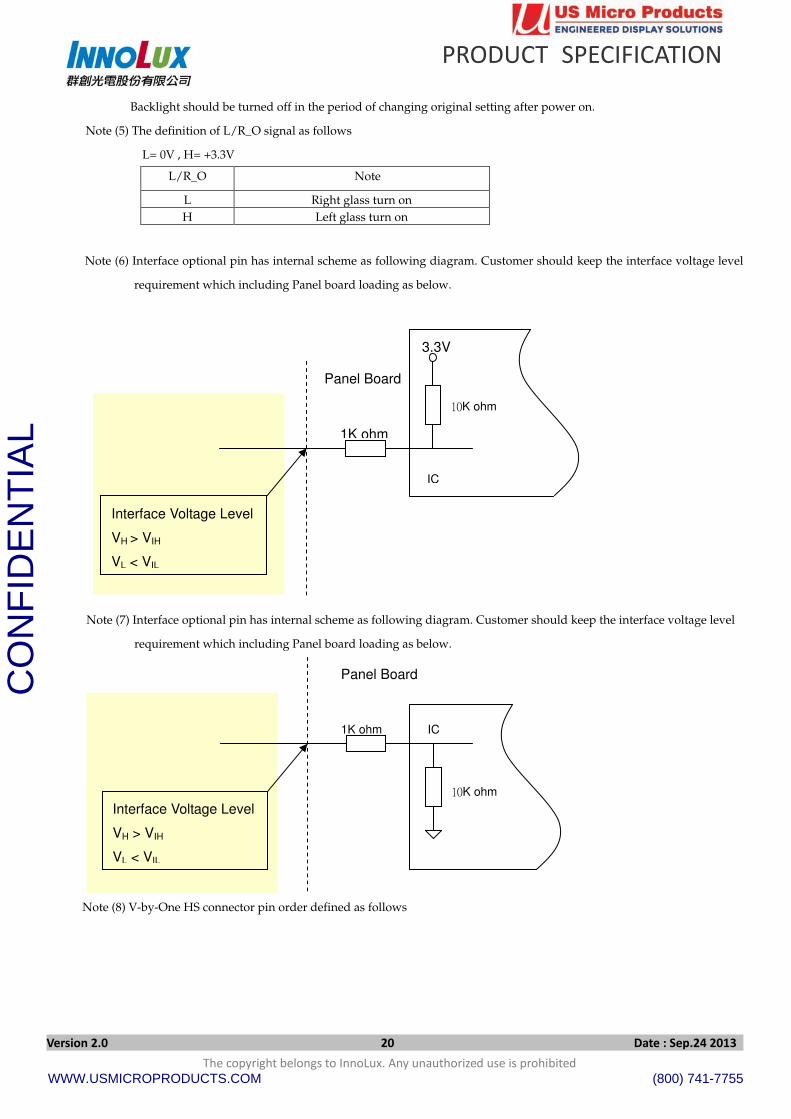
Backlight should be turned off in the period of changing original setting after power on.
Note (5) The definition of L/R_O signal as follows
L= 0V , H= +3.3V
L/R_O Note
L Right glass turn on
H Left glass turn on
Note (6) Interface optional pin has internal scheme as following diagram. Customer should keep the interface voltage level
requirement which including Panel board loading as below.
Note (7) Interface optional pin has internal scheme as following diagram. Customer should keep the interface voltage level
requirement which including Panel board loading as below.
Note (8) V-by-One HS connector pin order defined as follows
IC
10K ohm
1K ohm
Panel Board
Interface Voltage Level
VH > VIH
VL < VIL
IC
10K ohm
1K ohm
Panel Board
Interface Voltage Level
VH > VIH
VL < VIL
3.3V
WWW.USMICROPRODUCTS.COM (800) 741-7755
CO
NFI
DE
NTI
AL

PRODUCT SPECIFICATION
Version 2.0 21 Date : Sep.24 2013
The copyright belongs to InnoLux. Any unauthorized use is prohibited
Note (9) V-by-One connector mating dimension range request is 0.93mm~1.0mm as below
.
Note (10) Reserved for internal use. Please leave it open.
Note (11) Local dimming table select & User dimming adjust for customer use. (User dimming is available only at 2D Mode.
User dimming duty ratio is set at 100% (Max. Brightness) in 3D Mode.)
Note (12) The detail setting such as I2C command or timing requirement in FHD/QFHD is specified in INX
application note. It’s important and necessary to follow the specification either in product SPEC or
application note, otherwise it may lead to abnormal or no display. INX application note would be
provided by INX in the design-in stage.
5.2 BACKLIGHT UNIT
The pin configuration for the housing and leader wire is shown in the table below.
CN3
Connector Type : 196388-12041-3(P-TWO) or FF01-431-123A(FCN)
Pin No. Symbol Description
1 VLED+
2 VLED+
3 VLED+
Positive of LED string
4 NC NC
5 N-
6 N-
7 N-
8 N-
9 N-
10 N-
11 N-
12 N-
Negative of LED string
WWW.USMICROPRODUCTS.COM (800) 741-7755
CO
NFI
DE
NTI
AL

PRODUCT SPECIFICATION
Version 2.0 22 Date : Sep.24 2013
The copyright belongs to InnoLux. Any unauthorized use is prohibited
CN6
Connector Type : 196388-12041-3(P-TWO) or FF01-431-123A(FCN)
Pin No. Symbol Description
1 N-
2 N-
3 N-
4 N-
5 N-
6 N-
7 N-
8 N-
Negative of LED string
9 NC NC
10 VLED+
11 VLED+
12 VLED+
Positive of LED string
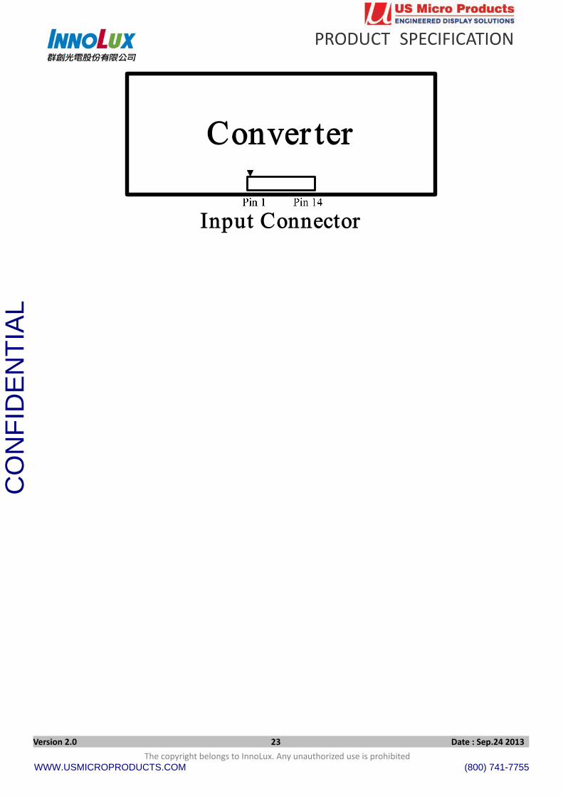
5.3 CONVERTER UNIT
CN1 (Header) : CI0114M1HR0-LA (CvilLux)
Pin No. Symbol Feature
1
2
3
4
5
VBL +24V
6
7
8
9
10
GND GND
11 ERR Normal (GND) ; Abnormal (Open collector)
12 BLON BL ON/OFF
13 NC NC
14 E_PWM External PWM Control
Note (1) If Pin14 is open, E_PWM is 100% duty.
Note (2) Input connector pin order defined as follows
WWW.USMICROPRODUCTS.COM (800) 741-7755
CO
NFI
DE
NTI
AL
PRODUCT SPECIFICATION
Version 2.0 23 Date : Sep.24 2013
The copyright belongs to InnoLux. Any unauthorized use is prohibited
WWW.USMICROPRODUCTS.COM (800) 741-7755
CO
NFI
DE
NTI
AL

PRODUCT SPECIFICATION
Version 2.0 24 Date : Sep.24 2013
The copyright belongs to InnoLux. Any unauthorized use is prohibited
5.4 COLOR DATA INPUT ASSIGNMENT
The brightness of each primary color (red, green and blue) is based on the 10-bit gray scale data input for the
color. The higher the binary input the brighter the color. The table below provides the assignment of color versus
data input.
Data Signal
Red Green Blue Color
R9 R8 R7 R6 R5 R4 R3 R2 R1 R0 G9 G8 G7 G6 G5 G4 G3 G2 G1 G0 B9 B8 B7 B6 B5 B4 B3 B2 B1 B0
Basic Colors
Black Red Green Blue Cyan Magenta Yellow White
0 1 0 0 0 1 1 1
0 1 0 0 0 1 1 1
0 1 0 0 0 1 1 1
0 1 0 0 0 1 1 1
0 1 0 0 0 1 1 1
0 1 0 0 0 1 1 1
0 1 0 0 0 1 1 1
0 1 0 0 0 1 1 1
0 1 0 0 0 1 1 1
0 1 0 0 0 1 1 1
0 0 1 0 1 0 1 1
0 0 1 0 1 0 1 1
0 0 1 0 1 0 1 1
0 0 1 0 1 0 1 1
0 0 1 0 1 0 1 1
0 0 1 0 1 0 1 1
0 0 1 0 1 0 1 1
0 0 1 0 1 0 1 1
0 0 1 0 1 0 1 1
0 0 1 0 1 0 1 1
0 0 0 1 1 1 0 1
0 0 0 1 1 1 0 1
0 0 0 1 1 1 0 1
0 0 0 1 1 1 0 1
0 0 0 1 1 1 0 1
0 0 0 1 1 1 0 1
0 0 0 1 1 1 0 1
0 0 0 1 1 1 0 1
0 0 0 1 1 1 0 1
0 0 0 1 1 1 0 1
Gray Scale Of Red
Red (0) / Dark Red (1) Red (2)
: :
Red (1021) Red (1022) Red (1023)
0 0 0 1 1 1
0 0 0 1 1 1
0 0 0 : : 1 1 1
0 0 0 : : 1 1 1
0 0 0 : : 1 1 1
0 0 0 : : 1 1 1
0 0 0 : : 1 1 1
0 0 0 : : 1 1 1
0 0 1 : : 0 1 1
0 1 0 : : 1 0 1
0 0 0 : : 0 0 0
0 0 0 : : 0 0 0
0 0 0 : : 0 0 0
0 0 0 : : 0 0 0
0 0 0 : : 0 0 0
0 0 0 : : 0 0 0
0 0 0 : : 0 0 0
0 0 0 : : 0 0 0
0 0 0 : : 0 0 0
0 0 0 : : 0 0 0
0 0 0 : ; 0 0 0
0 0 0 : : 0 0 0
0 0 0 : : 0 0 0
0 0 0 : : 0 0 0
0 0 0 : : 0 0 0
0 0 0 : : 0 0 0
0 0 0 : : 0 0 0
0 0 0 : : 0 0 0
0 0 0 : : 0 0 0
0 0 0 : : 0 0 0
Gray Scale Of Green
Green (0) / Dark Green (1) Green (2)
: :
Green (1021) Green (1022) Green (1023)
0 0 0 : : 0 0 0
0 0 0 : : 0 0 0
0 0 0 : : 0 0 0
0 0 0 : : 0 0 0
0 0 0 : : 0 0 0
0 0 0 : : 0 0 0
0 0 0 : : 0 0 0
0 0 0 : : 0 0 0
0 0 0 : : 0 0 0
0 0 0 : : 0 0 0
0 0 0 : : 1 1 1
0 0 0 : : 1 1 1
0 0 0 : : 1 1 1
0 0 0 : : 1 1 1
0 0 0 : : 1 1 1
0 0 0 : : 1 1 1
0 0 0 : : 1 1 1
0 0 0 : : 1 1 1
0 0 1 : : 0 1 1
0 1 0 : : 1 0 1
0 0 0 : : 0 0 0
0 0 0 : : 0 0 0
0 0 0 : : 0 0 0
0 0 0 : : 0 0 0
0 0 0 : : 0 0 0
0 0 0 : : 0 0 0
0 0 0 : : 0 0 0
0 0 0 : : 0 0 0
0 0 0 : : 0 0 0
0 0 0 : : 0 0 0
Gray Scale Of Blue
Blue (0) / Dark Blue (1) Blue (2)
: :
Blue (1021) Blue (1022) Blue (1023)
0 0 0 : : 0 0 0
0 0 0 : : 0 0 0
0 0 0 : : 0 0 0
0 0 0 : : 0 0 0
0 0 0 : : 0 0 0
0 0 0 : : 0 0 0
0 0 0 : : 0 0 0
0 0 0 : : 0 0 0
0 0 0 : : 0 0 0
0 0 0 : : 0 0 0
0 0 0 : : 0 0 0
0 0 0 : : 0 0 0
0 0 0 : : 0 0 0
0 0 0 : : 0 0 0
0 0 0 : : 0 0 0
0 0 0 : : 0 0 0
0 0 0 : : 0 0 0
0 0 0 : : 0 0 0
0 0 0 : : 0 0 0
0 0 0 : : 0 0 0
0 0 0 : : 1 1 1
0 0 0 : : 1 1 1
0 0 0 : : 1 1 1
0 0 0 : : 1 1 1
0 0 0 : : 1 1 1
0 0 0 : : 1 1 1
0 0 0 : : 1 1 1
0 0 0 : : 1 1 1
0 0 1 : : 0 1 1
0 1 0 : : 1 0 1
Note (1) 0: Low Level Voltage,1: High Level Voltage
WWW.USMICROPRODUCTS.COM (800) 741-7755
CO
NFI
DE
NTI
AL
PRODUCT SPECIFICATION
Version 2.0 25 Date : Sep.24 2013
The copyright belongs to InnoLux. Any unauthorized use is prohibited
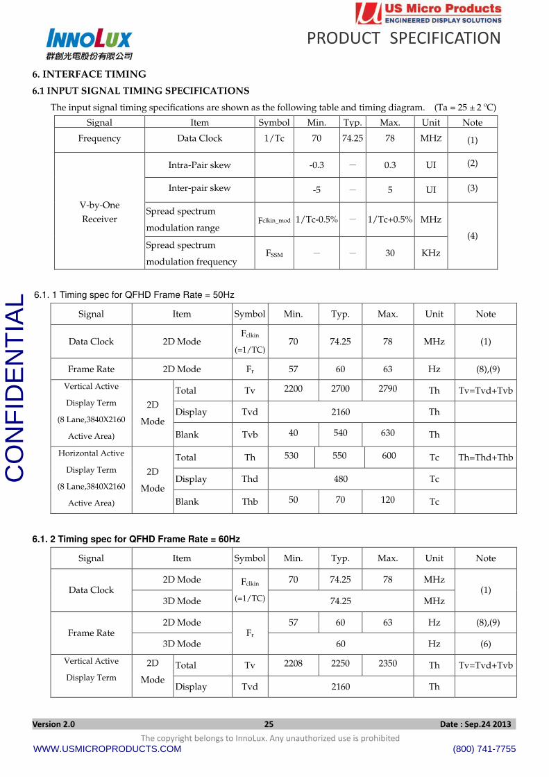
6. INTERFACE TIMING
6.1 INPUT SIGNAL TIMING SPECIFICATIONS
The input signal timing specifications are shown as the following table and timing diagram. (Ta = 25 ± 2 ºC)
Signal Item Symbol Min. Typ. Max. Unit Note
Frequency Data Clock 1/Tc 70 74.25 78 MHZ (1)
Intra-Pair skew
-0.3 - 0.3 UI (2)
Inter-pair skew -5 - 5 UI (3)
Spread spectrum
modulation range Fclkin_mod 1/Tc-0.5% - 1/Tc+0.5% MHz
V-by-One
Receiver
Spread spectrum
modulation frequency FSSM - - 30 KHz
(4)
6.1. 1 Timing spec for QFHD Frame Rate = 50Hz
Signal Item Symbol Min. Typ. Max. Unit Note
Data Clock 2D Mode Fclkin
(=1/TC) 70 74.25 78 MHz (1)
Frame Rate 2D Mode Fr 57 60 63 Hz (8),(9)
Total Tv 2200 2700 2790 Th Tv=Tvd+Tvb
Display Tvd 2160 Th
Vertical Active
Display Term
(8 Lane,3840X2160
Active Area)
2D
Mode
Blank Tvb 40 540 630 Th
Total Th 530 550 600 Tc Th=Thd+Thb
Display Thd 480 Tc
Horizontal Active
Display Term
(8 Lane,3840X2160
Active Area)
2D
Mode
Blank Thb 50 70 120 Tc
6.1. 2 Timing spec for QFHD Frame Rate = 60Hz
Signal Item Symbol Min. Typ. Max. Unit Note
2D Mode 70 74.25 78 MHz Data Clock
3D Mode
Fclkin
(=1/TC) 74.25 MHz (1)
2D Mode 57 60 63 Hz (8),(9) Frame Rate
3D Mode Fr
60 Hz (6)
Total Tv 2208 2250 2350 Th Tv=Tvd+Tvb Vertical Active
Display Term
2D
Mode Display Tvd 2160 Th
WWW.USMICROPRODUCTS.COM (800) 741-7755
CO
NFI
DE
NTI
AL

PRODUCT SPECIFICATION
Version 2.0 26 Date : Sep.24 2013
The copyright belongs to InnoLux. Any unauthorized use is prohibited
Blank Tvb 48 90 190 Th
Total Tv 2250 Th
Display Tvd 2160 Th
(8 Lane,3840X2160
Active Area)
3D
Mode
Blank Tvb 90 Th (7)
Total Th 530 550 600 Tc Th=Thd+Thb
Display Thd 480 Tc 2D
Mode
Blank Thb 50 70 120 Tc
Total Th 530 550 600 Tc Th=Thd+Thb
Display Thd 480 Tc
Horizontal Active
Display Term
(8 Lane,3840X2160
Active Area)
3D
Mode
Blank Thb 50 70 120 Tc
6.1.3 Input Timing Spec for FHD, Frame Rate = 50Hz
Signal Item Symbol Min. Typ. Max. Unit Note
Data Clock Frequency Fclkin
(=1/TC) 70 74.25 78 MHz (1)
Frame Rate 2D Mode Fr 47 50 53 Hz (8),(9)
Total Tv 1104 1350 1395 Th Tv=Tvd+Tvb
Display Tvd 1080 Th
Vertical Active
Display Term
(2 Lane,1920X1080
Active Area) Blank Tvb 24 270 315 Th
Total Th 1060 1100 1340 Tc Th=Thd+Thb
Display Thd 960 Tc
Horizontal Active
Display Term
(2 Lane,1920X1080
Active Area)
2D
Mode
Blank Thb 100 140 380 Tc
6.1.4 Input Timing Spec for FHD, Frame Rate = 60Hz
Signal Item Symbol Min. Typ. Max. Unit Note
Data Clock Frequency Fclkin
(=1/TC) 70 74.25 78 MHz (1)
Frame Rate 2D Mode Fr 57 60 63 Hz (8),(9)
Total Tv 1104 1125 1395 Th Tv=Tvd+Tvb
Display Tvd 1080 Th
Vertical Active
Display Term
(2 Lane,1920X1080
Active Area)
2D
Mode
Blank Tvb 24 45 315 Th
WWW.USMICROPRODUCTS.COM (800) 741-7755
CO
NFI
DE
NTI
AL

PRODUCT SPECIFICATION
Version 2.0 27 Date : Sep.24 2013
The copyright belongs to InnoLux. Any unauthorized use is prohibited
Total Th 1060 1100 1340 Tc Th=Thd+Thb
Display Thd 960 Tc
Horizontal Active
Display Term
(2 Lane,1920X1080
Active Area)
Blank Thb 100 140 380 Tc
6.1.5 Input Timing Spec for FHD, Frame Rate = 100Hz
Signal Item Symbol Min. Typ. Max. Unit Note
Data Clock Frequency Fclkin
(=1/TC) 70 74.25 78 MHz (1)
Frame Rate 2D Mode Fr 97 100 103 Hz (8),(9)
Total Tv 1104 1350 1395 Th Tv=Tvd+Tvb
Display Tvd 1080 Th
Vertical Active
Display Term
(4 Lane,1920X1080
Active Area) Blank Tvb 24 270 315 Th
Total Th 530 550 670 Tc Th=Thd+Thb
Display Thd 480 Tc
Horizontal Active
Display Term
(4 Lane,1920X1080
Active Area)
2D
Mode
Blank Thb 50 70 190 Tc
6.1.6 Input Timing Spec for FHD, Frame Rate = 120Hz
Signal Item Symbol Min. Typ. Max. Unit Note
2D Mode 70 74.25 78 MHz Data Clock
3D Mode
Fclkin
(=1/TC) 74.25 MHz (1)
2D Mode 117 120 123 Hz (8),(9) Frame Rate
3D Mode Fr
120 Hz (6)
Total Tv 1104 1125 1395 Th Tv=Tvd+Tvb
Display Tvd 1080 Th 2D
Mode
Blank Tvb 24 45 315 Th
Total Tv 1125 Th
Display Tvd 1080 Th
Vertical Active
Display Term
(4 Lane,1920X1080
Active Area)
3D
Mode
Blank Tvb 45 Th (7)
Total Th 530 550 670 Tc Th=Thd+Thb
Display Thd 480 Tc
Horizontal Active
Display Term
(4 Lane,1920X1080
2D
Mode
Blank Thb 50 70 190 Tc
WWW.USMICROPRODUCTS.COM (800) 741-7755
CO
NFI
DE
NTI
AL
PRODUCT SPECIFICATION
Version 2.0 28 Date : Sep.24 2013
The copyright belongs to InnoLux. Any unauthorized use is prohibited
Total Th 530 550 670 Tc Th=Thd+Thb
Display Thd 480 Tc
Active Area)
3D
Mode
Blank Thb 50 70 190 Tc
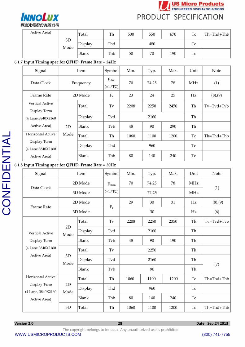
6.1.7 Input Timing spec for QFHD, Frame Rate = 24Hz
Signal Item Symbol Min. Typ. Max. Unit Note
Data Clock Frequency Fclkin
(=1/TC) 70 74.25 78 MHz (1)
Frame Rate 2D Mode Fr 23 24 25 Hz (8),(9)
Total Tv 2208 2250 2450 Th Tv=Tvd+Tvb
Display Tvd 2160 Th
Vertical Active
Display Term
(4 Lane,3840X2160
Active Area) Blank Tvb 48 90 290 Th
Total Th 1060 1100 1200 Tc Th=Thd+Thb
Display Thd 960 Tc
Horizontal Active
Display Term
(4 Lane,3840X2160
Active Area)
2D
Mode
Blank Thb 80 140 240 Tc
6.1.8 Input Timing spec for QFHD, Frame Rate = 30Hz
Signal Item Symbol Min. Typ. Max. Unit Note
2D Mode 70 74.25 78 MHz Data Clock
3D Mode
Fclkin
(=1/TC) 74.25 MHz (1)
2D Mode 29 30 31 Hz (8),(9) Frame Rate
3D Mode Fr
30 Hz (6)
Total Tv 2208 2250 2350 Th Tv=Tvd+Tvb
Display Tvd 2160 Th 2D
Mode
Blank Tvb 48 90 190 Th
Total Tv 2250 Th
Display Tvd 2160 Th
Vertical Active
Display Term
(4 Lane,3840X2160
Active Area)
3D
Mode
Blank Tvb 90 Th (7)
Total Th 1060 1100 1200 Tc Th=Thd+Thb
Display Thd 960 Tc 2D
Mode
Blank Thb 80 140 240 Tc
Horizontal Active
Display Term
(4 Lane, 3840X2160
Active Area)
3D Total Th 1060 1100 1200 Tc Th=Thd+Thb
WWW.USMICROPRODUCTS.COM (800) 741-7755
CO
NFI
DE
NTI
AL

PRODUCT SPECIFICATION
Version 2.0 29 Date : Sep.24 2013
The copyright belongs to InnoLux. Any unauthorized use is prohibited
Display Thd 960 Tc Mode
Blank Thb 1060 1100 1200 Tc
Note (1) Please make sure the range of pixel clock has follow the below equation:
Fclkin(max) Fr Tv Th≧ ≧ ≧
Fr Tv Th Fclkin (min) ≧ ≧ ≧
INPUT SIGNAL TIMING DIAGRAM
Note (2) Intra-pair Data skew
Note (3) V-by-One HS Inter-pair skew.
Tv
Tvd Tvb
Th
DE
Thb
Valid Display Data (480 DCLK)
Tc
DCLK
WWW.USMICROPRODUCTS.COM (800) 741-7755
CO
NFI
DE
NTI
AL
PRODUCT SPECIFICATION
Version 2.0 30 Date : Sep.24 2013
The copyright belongs to InnoLux. Any unauthorized use is prohibited
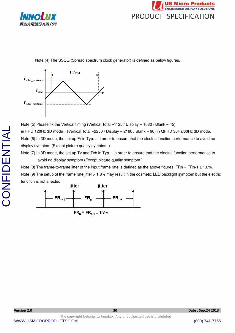
Note (4) The SSCG (Spread spectrum clock generator) is defined as below figures.
Note (5) Please fix the Vertical timing (Vertical Total =1125 / Display = 1080 / Blank = 45)
in FHD 120Hz 3D mode、(Vertical Total =2250 / Display = 2160 / Blank = 90) in QFHD 30Hz/60Hz 3D mode.
Note (6) In 3D mode, the set up Fr in Typ. . In order to ensure that the electric function performance to avoid no
display symptom.(Except picture quality symptom.)
Note (7) In 3D mode, the set up Tv and Tvb in Typ. . In order to ensure that the electric function performance to
avoid no display symptom.(Except picture quality symptom.)
Note (8) The frame-to-frame jitter of the input frame rate is defined as the above figures. FRn = FRn-1 ± 1.8%.
Note (9) The setup of the frame rate jitter > 1.8% may result in the cosmetic LED backlight symptom but the electric
function is not affected.
WWW.USMICROPRODUCTS.COM (800) 741-7755
CO
NFI
DE
NTI
AL

PRODUCT SPECIFICATION
Version 2.0 31 Date : Sep.24 2013
The copyright belongs to InnoLux. Any unauthorized use is prohibited
6.2 V by One Input Signal Timing Diagram
Y
X
X=0 UI X=1 UI
1UI = 1/(Serial data rate)
A
B C
D
E F
Y=0mV
Table 1 Eye Mask Specification
X [UI] Y [mV] Note
A 0.25 0 (1)
B 0.3 50 (1)
C 0.7 50 (1)
D 0.75 0 (1)
E 0.7 -50 (1)
F 0.3 -50 (1)
Note (1) Input levels of V-by-One HS signals are comes from “V-by-One HS Stander Ver.1.4”
6.3 Byte Length and Color mapping of V-by-One HS
Packer input &
Unpacker output 30bpp RGB (10bit)
D[0] R[2]
D[1] R[3]
D[2] R[4]
D[3] R[5]
D[4] R[6]
D[5] R[7]
D[6] R[8]
Byte 0
D[7] R[9]
Byte 1 D[8] G[2]
WWW.USMICROPRODUCTS.COM (800) 741-7755
CO
NFI
DE
NTI
AL

PRODUCT SPECIFICATION
Version 2.0 32 Date : Sep.24 2013
The copyright belongs to InnoLux. Any unauthorized use is prohibited
D[9] G[3]
D[10] G[4]
D[11] G[5]
D[12] G[6]
D[13] G[7]
D[14] G[8]
D[15] G[9]
D[16] B[2]
D[17] B[3]
D[18] B[4]
D[19] B[5]
D[20] B[6]
D[21] B[7]
D[22] B[8]
Byte 2
D[23] B[9]
D[24] X
D[25] X
D[26] B[0]
D[27] B[1]
D[28] G[0]
D[29] G[1]
D[30] R[0]
Byte 3
D[31] R[1]
WWW.USMICROPRODUCTS.COM (800) 741-7755
CO
NFI
DE
NTI
AL

PRODUCT SPECIFICATION
Version 2.0 33 Date : Sep.24 2013
The copyright belongs to InnoLux. Any unauthorized use is prohibited
0.5≦T1≦10ms
0≦T2
0≦T3
500ms ≦T4
10ms <T16
0≦T17
50%
0V
0V
50%
T3
T1
0.1Vcc 0.1Vcc
T4
T2
Power On Power Off
V-By-One Signals
Backlight (Recommended)
1500ms≦T5
100ms≦T6
T7 T8
Option Signals (2D/3D, LD_EN, L/R)
0≦T7≦T2
0≦T8≦T3
0.9Vcc 0.9Vcc
Host I2C Command
1200ms≦T13
T13
T14
HTPDN
LOCKN
CDR
Training
Valid
Data
T17
T16
6.4 POWER ON/OFF SEQUENCE
(Ta = 25 ± 2 ºC)
To prevent a latch-up or DC operation of LCD module, the power on/off sequence should be as the diagram
below.
0V
Vcc(typ.) x 0.85
Vcc Dip
T15≦10ms
WWW.USMICROPRODUCTS.COM (800) 741-7755
CO
NFI
DE
NTI
AL
PRODUCT SPECIFICATION
Version 2.0 34 Date : Sep.24 2013
The copyright belongs to InnoLux. Any unauthorized use is prohibited
6.5 2D/3D MODE CHANGE SIGNAL SEQUENCE WITHOUT VCC TURN OFF AND TURN ON
Note (1) The supply voltage of the external system for the module input should follow the definition of Vcc.
Note (2) Apply the LED voltage within the LCD operation range. When the backlight turns on before the LCD operation or
the LCD turns off before the backlight turns off, the display may momentarily become abnormal screen.
Note (3) In case of Vcc is in off level, please keep the level of input signals on the low or high impedance. If T2<0,that maybe
cause electrical overstress failure.
Note (4) T4 should be measured after the module has been fully discharged between power off and on period.
Note (5) Interface signal shall not be kept at high impedance when the power is on.
Note (6) When 2D/3D mode is changed, TCON will insert black pattern internally. During black insertion, TCON would
load required optical table and TCON parameter setting. The black insertion time should be longer than 650ms
because TCON must recognize 2D or 3D format and set the correct parameter.
Note (7) Vcc must decay smoothly when power-off.
Note (8) T5 Backlight turn on time depend on T14 command length+T13
WWW.USMICROPRODUCTS.COM (800) 741-7755
CO
NFI
DE
NTI
AL

PRODUCT SPECIFICATION
Version 2.0 35 Date : Sep.24 2013
The copyright belongs to InnoLux. Any unauthorized use is prohibited
7. OPTICAL CHARACTERISTICS
7.1 TEST CONDITIONS
Item Symbol Value Unit
Ambient Temperature Ta 25±2 oC
Ambient Humidity Ha 50±10 %RH
Supply Voltage VCC 12±1.2 V
Input Signal According to typical value in "3. ELECTRICAL CHARACTERISTICS"
Vertical Frame Rate Fr 60 Hz
The LCD module should be stabilized at given temperature for 1 hour to avoid abrupt temperature change
during measuring in a windless room.
Local Dimming Function should be Disable before testing to get the steady optical characteristics (According to
5.1 CNF1 Connector Pin Assignment, Pin no. “42”)
CS - 2000
500 mm
LCD Module
LCD Panel
Field of View = 1º
Light Shield Room
(Ambient Luminance < 2 lux)
WWW.USMICROPRODUCTS.COM (800) 741-7755
CO
NFI
DE
NTI
AL
PRODUCT SPECIFICATION
Version 2.0 36 Date : Sep.24 2013
The copyright belongs to InnoLux. Any unauthorized use is prohibited
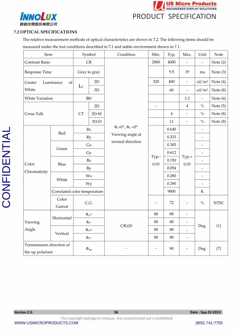
7.2 OPTICAL SPECIFICATIONS
The relative measurement methods of optical characteristics are shown in 7.2. The following items should be
measured under the test conditions described in 7.1 and stable environment shown in 7.1.
Item Symbol Condition Min. Typ. Max. Unit Note
Contrast Ratio CR 2800 4000 - - Note (2)
Response Time Gray to gray 9.5 19 ms Note (3)
2D 320 400 - cd/m2 Note (4) Center Luminance of
White LC
3D 60 - cd/m2 Note (8)
White Variation δW 1.3 - Note (6)
2D - 4 % Note (5)
3D-W 4 - % Note (8) Cross Talk CT
3D-D 11 - % Note (8)
Rx 0.640 - Red
Ry 0.333 -
Gx 0.305 - Green
Gy 0.612 -
Bx 0.150 - Blue
By 0.054 -
Wx 0.280 - White
Wy 0.290 -
Correlated color temperature
Typ.-
0.03
9800
Typ.+
0.03
K
Color
Chromaticity
Color
Gamut C.G.
θx=0° , θY =0°
Viewing angle at
normal direction
- 72 - % NTSC
θx+ 80 88 - Horizontal
θx- 80 88 -
θY+ 80 88 -
Viewing
Angle Vertical
θY-
CR≥20
80 88 -
Deg. (1)
Transmission direction of
the up polarizer Φup - - 90 - Deg. (7)
WWW.USMICROPRODUCTS.COM (800) 741-7755
CO
NFI
DE
NTI
AL

PRODUCT SPECIFICATION
Version 2.0 37 Date : Sep.24 2013
The copyright belongs to InnoLux. Any unauthorized use is prohibited
Note (1) Definition of Viewing Angle (θx, θy) :
Viewing angles are measured by Autronic Conoscope Cono-80 (or Eldim EZ-Contrast 160R).
Note (2) Definition of Contrast Ratio (CR) :
The contrast ratio can be calculated by the following expression.
Contrast Ratio (CR) = L0 of Luminance Surface
L1023 of Luminance Surface
L1023: Luminance of gray level 1023
L 0: Luminance of gray level 0
CR = CR (5), where CR (X) is corresponding to the Contrast Ratio of the point X at the figure in Note (6).
Note (3) Definition of Gray-to-Gray Switching Time :
The driving signal means the signal of gray level 0, 124, 252, 380, 508, 636, 764, 892 and 1023.
Gray to gray average time means the average switching time of gray level 0, 124, 252, 380, 508, 636, 764, 892 and 1023 to each
other.
Note (4) Definition of Luminance of White (LC) :
12 o’clock direction
θy+ = 90º
6 o’clock
θy- = 90º
θx−
θx+
θy- θy+
x- y+
y- x+
Normal
θx = θy = 0º
θX+ = 90º
θX- = 90º
WWW.USMICROPRODUCTS.COM (800) 741-7755
CO
NFI
DE
NTI
AL

PRODUCT SPECIFICATION
Version 2.0 38 Date : Sep.24 2013
The copyright belongs to InnoLux. Any unauthorized use is prohibited
Measure the luminance of gray level 1023 at center point.
LC = L (5), where L (x) is corresponding to the luminance of the point X at the figure in Note (6).
Note (5) Definition of Cross Talk (CT) :
CT = | YB – YA | / YA × 100 (%)
Where :
YA = Luminance of measured location without gray level 1023 pattern (cd/m2)
YB = Luminance of measured location with gray level 1023 pattern (cd/m2)
Note (6) Definition of White Variation (δW):
Measure the luminance of gray level 1023 at 5 points
δW = (5)] L (4), L (3), L (2), L (1), [L Minimum
(5)] L (4), L (3), L (2), L (1), [L Maximum
Active Area
YA, R (7D/8,W/2)
YA, D (D/2,7W/8)
(0, 0)
(D, W)
Gray 512
Active Area
YB, U (D/2,W/8)
(0, 0)
YB, D (D/2,7W/8)
YB, L (D/8,W/2)
Gray 1023
YA,U (D/2,W/8)
YA,L (D/8,W/2) YA, R (7D/8,W/2)
(D/4,W/4)
(3D/4,3W/4)
WWW.USMICROPRODUCTS.COM (800) 741-7755
CO
NFI
DE
NTI
AL

PRODUCT SPECIFICATION
Version 2.0 39 Date : Sep.24 2013
The copyright belongs to InnoLux. Any unauthorized use is prohibited
Note (7) This is a reference for designing the shutter glasses of 3D application. Definition of the transmission direction of the up
polarizer (Φup-P) on LCD Module :
The transmission axis of the front polarizer of the shutter glasses should be parallel to this panel transmission direction to
get a maximum 3D mode luminance.
y+
6 o’clock
x-
x+
Φ=0o
y-
Φup-P
12 o’clock direction
Up Polarizer
WWW.USMICROPRODUCTS.COM (800) 741-7755
CO
NFI
DE
NTI
AL

PRODUCT SPECIFICATION
Version 2.0 40 Date : Sep.24 2013
The copyright belongs to InnoLux. Any unauthorized use is prohibited
Note (8) Definition of the 3D mode performance (measured under 3D mode, use INX’s shutter glass) :
a. Test pattern
Left eye image and right eye image are displayed alternated
b. Measurement setup
Shutter glasses are well controlled under suitable timing, and measure the luminance of the center point of the panel
through the right eye glass. The transmittance of the glass should be larger than 40.0% under 3D mode operation.
The luminance of the test pattern “WW”, denoted L(WW); the luminance of the test pattern ”WB”, denoted L(WB) ;
the luminance of the test pattern “BW”, denoted L(BW); the luminance of the test pattern “BB”, denoted “L(BB)
c. Definition of the Center Luminance of White, Lc (3D) : L(WW)
d. Definition of the 3D mode white crosstalk, CT (3D-W) : )()(
)()()3(
BBLWWL
BBLWBLWDCT
−
−≡−
e. Definition of the 3D mode dark crosstalk, CT (3D-D) : )()(
)()()3(
BBLWWL
BWLWWLDDCT
−
−≡−
WW
Left eye image: W1023; Right eye image: W1023
WB
Left eye image: W1023; Right eye image: W0
BW
Left eye image: W0; Right eye image: W1023
BB
Left eye image: W0; Right eye image: W0
CS - 2000
500 mm
LCD Module
LCD Panel
Field of View = 1º
Light Shield Room
(Ambient Luminance < 2 lux)
Right Eye Shutter Glass
WWW.USMICROPRODUCTS.COM (800) 741-7755
CO
NFI
DE
NTI
AL

PRODUCT SPECIFICATION
Version 2.0 41 Date : Sep.24 2013
The copyright belongs to InnoLux. Any unauthorized use is prohibited
8. PRECAUTIONS
8.1 ASSEMBLY AND HANDLING PRECAUTIONS
(1) Do not apply rough force such as bending or twisting to the module during assembly.
(2) It is recommended to assemble or to install a module into the user’s system in clean working areas. The
dust and oil may cause electrical short or worsen the polarizer.
(3) Do not apply pressure to the module (including Active Area) to prevent the damage of LCD panel and
backlight.
(4) Always follow the correct power-on sequence when the LCD module is turned on. This can prevent the
damage and latch-up of the CMOS LSI chips.
(5) Do not plug in or pull out the I/F connector while the module is in operation.
(6) Do not disassemble the module.
(7) Use a soft dry cloth without chemicals for cleaning, because the surface of polarizer is very soft and
easily scratched.
(8) Moisture can easily penetrate into LCD module and may cause the damage during operation.
(9) High temperature or humidity may deteriorate the performance of LCD module. Please store LCD
modules in the specified storage conditions.
(10) When ambient temperature is lower than 10ºC, the display quality might be reduced. For example, the
response time will become slow, and the starting voltage of LED will be higher than that of room
temperature.
8.2 SAFETY PRECAUTIONS
(1) The startup voltage of a backlight is over 1000 Volts. It may cause an electrical shock while assembling
with the inverter. Do not disassemble the module or insert anything into the backlight unit.
(2) If the liquid crystal material leaks from the panel, it should be kept away from the eyes or mouth. In
case of contact with hands, skin or clothes, it has to be washed away thoroughly with soap.
(3) After the module’s end of life, it is not harmful in case of normal operation and storage.
8.3 SAFETY STANDARDS
The LCD module should be certified with safety regulations as follows:
Regulatory Item Standard
UL UL60950-1:2006 or Ed.2:2007
cUL CAN/CSA C22.2 No.60950-1-03 or 60950-1-07
Information Technology
equipment
CB IEC60950-1:2005 / EN60950-1:2006+ A11:2009
UL UL60065 Ed.7:2007
cUL CAN/CSA C22.2 No.60065-03:2006 + A1:2006 Audio/Video Apparatus
CB IEC60065:2001+ A1:2005 / EN60065:2002 + A1:2006+ A11:2008
If the module displays the same pattern for a long period of time, the phenomenon of image sticking may be occurred.
WWW.USMICROPRODUCTS.COM (800) 741-7755
CO
NFI
DE
NTI
AL

PRODUCT SPECIFICATION
Version 2.0 42 Date : Sep.24 2013
The copyright belongs to InnoLux. Any unauthorized use is prohibited
9. DEFINITION OF LABELS
9.1 MODULE LABEL
The barcode nameplate is pasted on each module as illustration, and its definitions are as following explanation.
Model Name : V500DK2-KS1
Revision : Rev. XX, for example: A0, A1… B1, B2… or C1, C2…etc.
Serial ID : X X X X X X X Y M D L N N N N
Serial ID includes the information as below :
Manufactured Date :
Year : 2001=1, 2002=2, 2003=3, 2004=4…2010=0, 2011=1, 2012=2…
Month: 1~9, A~C, for Jan. ~ Dec.
Day: 1~9, A~Y, for 1st to 31st, exclude I ,O, and U.
Revision Code : Cover all the change
Serial No. : Manufacturing sequence of product
Product Line : 1→Line1, 2→Line 2, …etc.
Product Line
Year, Month, Date
INX Internal Use
INX Internal Use
Revision
INX Internal Use
Serial No.
MADE IN CHINA
LEOO(CAPG/CANO/VIRO)
RoHS X X X X X X X Y M D L N N N N
V500DK2-KS1 Rev. XX
WWW.USMICROPRODUCTS.COM (800) 741-7755
CO
NFI
DE
NTI
AL

PRODUCT SPECIFICATION
Version 2.0 43 Date : Sep.24 2013
The copyright belongs to InnoLux. Any unauthorized use is prohibited
9.2 CARTON LABEL
The barcode nameplate is pasted on each box as illustration, and its definitions are as following explanation.
Model Name: V500DK2– KS1
Carton ID: X X X X X X X Y M D X X X X
Serial ID includes the information as below :
Manufactured Date:
Year: 2010=0, 2011=1, 2012=2…etc.
Month: 1~9, A~C, for Jan. ~ Dec.
Day: 1~9, A~Y, for 1st to 31st, exclude I ,O, and U.
Revision Code: Cover all the change
P.O. NO.
Parts ID.
Model Name V500DK2-KS1
Carton ID. Quantities
XXXXXXXXXXXXXX
Made In Taiwan (Made In China)
INX Internal Use
Year, Month, Date
INX Internal Use
Revision
WWW.USMICROPRODUCTS.COM (800) 741-7755
CO
NFI
DE
NTI
AL
PRODUCT SPECIFICATION
Version 2.0 44 Date : Sep.24 2013
The copyright belongs to InnoLux. Any unauthorized use is prohibited
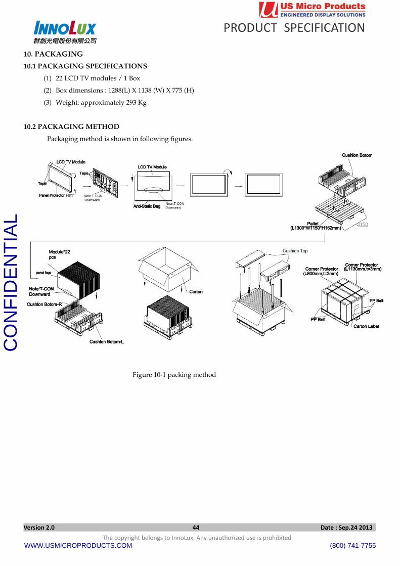
10. PACKAGING
10.1 PACKAGING SPECIFICATIONS
(1) 22 LCD TV modules / 1 Box
(2) Box dimensions : 1288(L) X 1138 (W) X 775 (H)
(3) Weight: approximately 293 Kg
10.2 PACKAGING METHOD
Packaging method is shown in following figures.
Figure 10-1 packing method
WWW.USMICROPRODUCTS.COM (800) 741-7755
CO
NFI
DE
NTI
AL

PRODUCT SPECIFICATION
Version 2.0 45 Date : Sep.24 2013
The copyright belongs to InnoLux. Any unauthorized use is prohibited
10.3 UN-PACKAGING METHOD
Un-packaging method is shown in following figures.
Figure 10-2 packing method
Figure 10-3 un-packing method
WWW.USMICROPRODUCTS.COM (800) 741-7755
CO
NFI
DE
NTI
AL
PRODUCT SPECIFICATION
Version 2.0 46 Date : Sep.24 2013
The copyright belongs to InnoLux. Any unauthorized use is prohibited
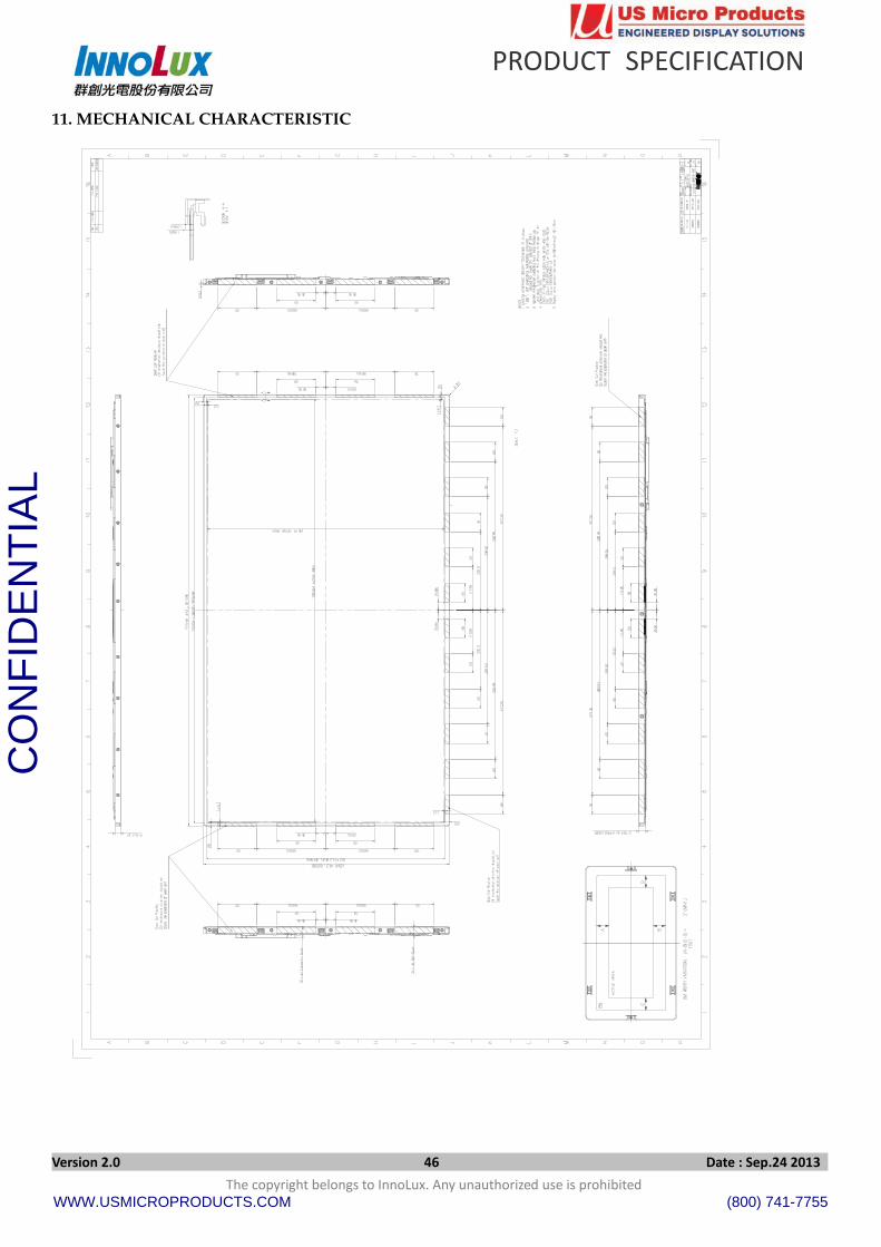
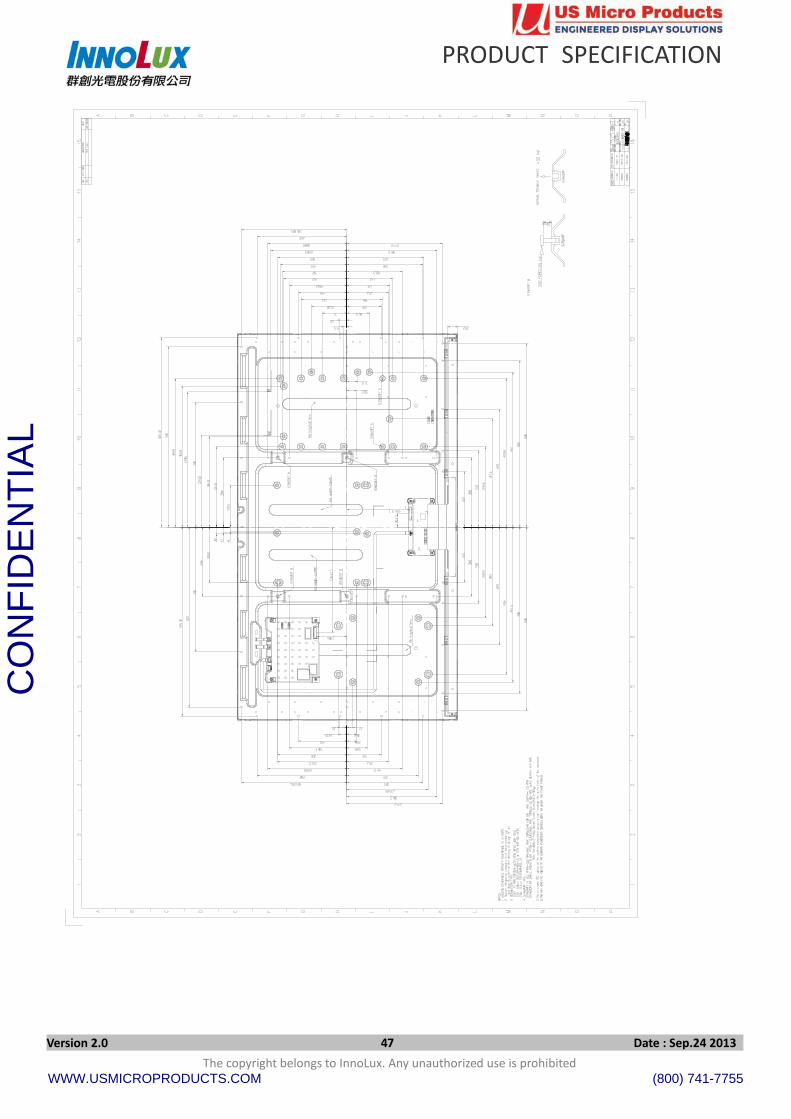
11. MECHANICAL CHARACTERISTIC
WWW.USMICROPRODUCTS.COM (800) 741-7755
CO
NFI
DE
NTI
AL
PRODUCT SPECIFICATION
Version 2.0 47 Date : Sep.24 2013
The copyright belongs to InnoLux. Any unauthorized use is prohibited
WWW.USMICROPRODUCTS.COM (800) 741-7755
CO
NFI
DE
NTI
AL

PRODUCT SPECIFICATION
Version 2.0 48 Date : Sep.24 2013
The copyright belongs to InnoLux. Any unauthorized use is prohibited
WWW.USMICROPRODUCTS.COM (800) 741-7755
CO
NFI
DE
NTI
AL

LOS ANGELES • AUSTIN • NEW YORK • LONDON • SHENZHEN • TAICHUNG800-741-7755
OLEDs TFTs Open Frame Monitors
Passive LCDs Multitouch Touch Screen
As our customer, you receive expert knowledge, support and service.Our technical sales staff and experienced design engineers provide answersto your questions and engineered solutions to meet your displays needs.
Keyboards TrackballsAerospaceTrackballs Printers
DISPLAYSEngineered to fit your application, US Micro Products offers a wide range of standard and custom LCD solutions. We dedicate ourselves to providing the best in displays forthe medical, industrial, gaming, automorive, aerospace, military and consumer markets.
PERIPHERALDEVICES
Our full line of peripheral devices includes keyboards, trackballs, and printers. These rugged industrial products are designed to meet your demanding requirements and are available as both standard and customs solutions.
6207 Bee Caves Rd. Suite 330, Austin Tx 78746US Tel. 800-741-7755 International Tel. 01-512-385-9000
www.usmicroproducts.com