Embed Size (px)
Citation preview

Laboratory Manual
Fundamentals of Electricity and Electronics - TECH 261 Ohio Northern University
Department of Technological Studies Dr. Adam W. Stienecker

Fundamentals of Electricity and Electronics TECH 261
Ohio Northern University
Table of Contents
1. Intro to The NI ELVIS Page 1
2. Changing a fuse in NI ELVIS Page 5
3. Lab 1 – Measuring Simple Circuits Page 6
4. Lab 2 – Simple circuits with ELVIS Page 7
5. Lab 3 – AC Circuits Page 8
6. Lab 4 – Resonance and Filtering Page 10
7. Lab 5 – Transistors Page 12
8. Lab 6 – Motor Controls Page 17
9. Lab 7 – Op-amp Basics Page 20
10. Lab 8 – Measuring Op-amp Parameters Page 22
11. Lab 9 – Cascading Op-amps Page 25
12. Example Lab Report Page 27
13. Lab reports guidelines Page 30
14. PN2222 Datasheet Page 31
15. TL3472 Datasheet Page 39

Fundamentals of Electricity and Electronics TECH 261
Ohio Northern University
Introduction to The NI ELVIS In order to experiment with electronics we need a place to house and facilitate the activities associated with the experiment. This requires measuring instruments, power supplies, signal generators, and digital controls and indicators. In the electronics lab we will be doing the majority of our experiments on the National Instruments Educational Laboratory Virtual Instrumentation Suite or NI ELVIS, referred to herein as ELVIS. ELVIS has the ability to supply DC power to our experiment at +5V, +15V, -15V, as well as a ± 12V variable supply. The system can also generate a sine, triangle, and square wave at a range of frequencies, DC amplitudes, and DC offsets. We can also use the system to control and verify digital signals as well as read analog signals. Most important to the system is its ability to facilitate the connection of wires or components to one another through a series of hundreds of small holes. Each hole in the board has a series of other holes that are electrically connected to one another internally. Studying the following pictures should clarify this.
The picture to the right shows a small section of the breadboard part of the ELVIS system. As mentioned above one ability that the system gives us is the ability to connect wires together. Shown in the figure are several boxes each surrounding five holes within the board. These five holes are internally electrically connected to one another. In other words, plugging one wire into the hole labeled 1 and one into the hole labeled 2 would cause the two wires to be electrically connected. Each hole within a grouping on the ELVIS breadboard is connected to the other holes in the grouping. There are also sections of five holes that are connected together. In the rows labeled W, X, Y, and Z there are five sections of five holes that are connected to one another. This allows the user to connect up to 25 wires to one another.
The picture to the left shows two wires plugged in to one grouping. These two wires are electrically connected because they are plugged in to the same grouping. On the next page you will find a series of pictures detailing how to connect different components to the board. Don’t worry if you don’t yet know what the components are, we’ll get to them later in the quarter.
1
2
1

Fundamentals of Electricity and Electronics TECH 261
Ohio Northern University
Introduction to The NI ELVIS
To resistors connected together in column 48.
A common mistake; a resistor with both leads connected together.
The transistor on the left is correctly installed. Note that each lead of the device has its own grouping in which to connect other wires or devices. The transistor on the right is installed incorrectly as all three of its leads are electrically connected together.
2

Fundamentals of Electricity and Electronics TECH 261
Ohio Northern University
Introduction to The NI ELVIS This picture shows two chips. The one on the left is installed incorrectly. Notice that on the correctly installed chip on the right each lead has its own grouping of five to connect to.
Also on the ELVIS board are connections to the other features in the system. These connections are located on both the left and right sides of the board. The white strip board with the square ‘3M’ label contains the connections to all these features. Below is a series of pictures detailing some of the more utilized connections.
On the left, starting from the top, is the Digital Multimeter (DMM) section. This section allows the user to measure parameters such as voltage or current on the computer screen. Voltage HI, Voltage LO, Current HI, and Current LO are the four predominant connections you will utilize throughout the quarter.
Continuing down under the Function Generator section we
find the FUNC OUT connection. This connection will be used to produce sine, triangle, and square waves for use in our circuits.
The Variable Power Supplies section contains connections
to the variable power supplies which can be varied via computer control.
Finally, under the DC Power Supplies section you will find
+15V, -15V, and +5V connections to power your circuits. This entire section of connections is located on the lower
left of the ELVIS breadboard.
3

Fundamentals of Electricity and Electronics TECH 261
Ohio Northern University
Introduction to The NI ELVIS
Also located on the left side of the board are the Dual channel Oscilloscope connections. The Oscilloscope allows you to see the waveform that is connected to it. It will plot the voltage level versus time with many different on screen controls. The remainder of the connections here will not be utilized in class.
On the right side of the board are the digital connections. Starting from the top is DI0 through DI7. These connections are digital inputs to your circuit. They allow you to control your digital circuit via computer software. Below that is another set of eight; DO0 through DO7. These are outputs from your circuit to the computer. These allow you to monitor a digital output on the computer screen. On the lower right of the picture is a series of eight Light Emitting Diodes (LEDs). When their associated connection (on the lower right section of the board, not shown here) is connected to a ‘1’ or a high signal they light up and if they are connected to a ‘0’ or a low signal or not connect at all they do not light up. These connections are labeled LED0 through LED7.
4

Fundamentals of Electricity and Electronics TECH 261
Ohio Northern University
Changing a fuse in NI ELVIS
Located on the board in the lower right corner are three LEDs that function as power supply indicators. One of the inherent problems in experimenting with electronics is creating a short circuit that draws more current than can be supplied through the internal fuses. When this happens a fuse is blown and must be changed. If, at any time, any or all of the three LEDs, as shown below, goes out then the following procedure must be followed to change the fuse.
1. Take note of the LEDs are out by noting the label underneath the LED. 2. Turn off both power switches and remove both cables at the rear of the ELVIS system. 3. As in the picture below, remove the breadboard by pulling down on the board. 4. Loosen the four thumbscrews on the back of the system and remove the back by pulling out, away from
the system. You should see the following.
5. Locate the fuse labeled the same as the LED that turned off, remove it, and replace it with a new one. Before continuing, discard the blown fuse.
6. Reattach the back, tighten the thumbscrews, reattach the cables, reinsert the breadboard, and turn on the power. You should be back in business.
5

Fundamentals of Electricity and Electronics TECH 261
Ohio Northern University
Name:_____________________________ 1. Build the circuit below using five alligator clip wires, one power supply set to 9V, and three resistors. 2. Using a multimeter, measure the following values.
VR1 (the voltage across R1) = ___________ VR2 (the voltage across R2) = ___________ VR3 (the voltage across R3) = ___________
IT (the current through R1) = ___________ IR2 (the current through R2) = ___________ IR3 (the current through R3) = ___________
V1 (the voltage of the power supply) = _________ 3. Disassemble the circuit and measure the value of the resistors with the multimeter and compare the measured value to the color coded value on each resistor. Are all three resistors within tolerance? R1: Measured Value _____ Color Code Colors _____ _____ _____ _____ Value/Range ______ _________ R2: Measured Value _____ Color Code Colors _____ _____ _____ _____ Value/Range ______ _________ R3: Measured Value _____ Color Code Colors _____ _____ _____ _____ Value/Range ______ _________ 4. Using only the measured value of the power supply and the measured value of the resistors, calculate the expected values of VR1, VR2, VR3, IT, IR2, and IR3 that you measured in number 2 above. Are they the same or similar to your measured values? Why or why not? 5. Calculate the power dissipated in each resistor as well as the total power consumed by the circuit. At $0.10 per kWh how much would this circuit cost to run for one year? 6. If your power supply was a battery with a capacity of 1500mAh how long would the battery last in this circuit? (Assume a linear battery capacity curve, i.e. C1.5 = C0.01).
Lab 1 - Measuring Simple Circuits
R1
1k
R3
6.8k
V1
9VdcR2
2.2k
6
Fundamentals of Electricity and Electronics TECH 261
Ohio Northern University
Name:_____________________________
1. Build the circuit below using the NI ELVIS system. 2. Using the NI ELVIS computer software, measure the following values. To measure voltage, use VOLTAGE HI and VOLTAGE LO, to measure current (disconnect your circuit) and use CURRENT HI and CURRENT LO. To measure resistance, put the resistor in CURRENT HI and CURRENT LO.
VR1 (the voltage across R1) = ___________ R1 = __________
VR2 (the voltage across R2) = ___________ R2 = __________
VR3 (the voltage across R3) = ___________ R3 = __________
VR4 (the voltage across R4) = ___________ R4 = __________
VR5 (the voltage across R5) = ___________ R5 = __________
V1 (power supply voltage) = ____________
IT (power supply current) = _____________ IR3 (the current through R3) = ___________
IR1 (the current through R1) = ___________ IR4 (the current through R4) = ___________
IR2 (the current through R2) = ___________ IR5 (the current through R5) = ___________ 3. Calculate the expected values that you measured in number 2 above. Use the measured value of the power supply given above as the expected value. Use the measured value of the resistors in your calculations as well. 4. Calculate the power dissipated in each resistor as well as the total power consumed. 5. If the electric company charged $0.05 per kWh, what would be the charge to power this circuit for one year?
Lab 2 - Simple circuits with ELVIS
R5510 Ohms
R3910 Ohms
R1
180 Ohms
R4560 Ohms
V115VDC
R2
240 Ohms
7

CH B+
CH B-
GROUND
FUNC OUT
VOLTAGE LO
VOLTAGE HI
L
R
Vac R
L
Fundamentals of Electricity and Electronics TECH 261
Ohio Northern University
Name:_____________________________
1. Obtain the provided inductor and a 240 Ohm resistor. 2. Turn on the NI ELVIS hardware (both front and rear switches). 3. Open NI ELVIS (START / All Programs / National Instruments / NI ELVIS 1.0 / NI ELVIS) 4. Click on the Digital Multimeter and select resistance, Ω. 5. Plug the resistor into CURRENT HI and CURRENT LO and record the resistance on the multimeter. 6. Remove the resistor and replace it with the inductor. Click over to Inductance (looks like a coil). 7. Measure the inductance of the inductor and record it below. 8. Click back to resistance and measure the resistance of the inductor and record it below. 9. Remove the inductor from the board and close the “Digital Multimeter.”
Resistor’s Resistance ______ Inductor’s Resistance _______ Inductor’s Inductance _______
10. Construct the following circuit (on the left) on your board. This is the same as the circuit on the right.
FUNC OUT and GROUND are your AC Voltage Source, VOLTAGE HI and VOLTAGE LO are used to measure the voltage drop across the inductor, and CH B+ and CH B- are used to measure the voltage drop across the resistor.
The following is a procedure to measure the phase difference between the voltage and the current in the
circuit. The connection to the inductor from the VOLTAGE HI and the VOLTAGE LO will cause a display of the voltage, VL, waveform on your screen. The voltage, VR, across the resistor is out of phase with VL but in phase with the current; therefore, we can display the waveform of VR (given by CH B+ and CH B-) on the screen to find the phase difference between the current and the voltage.
11. Open the “Function Generator” in NI ELVIS. 12. Click “ON” to turn it on (the manual switch on the front panel in the function generator box must be
in the down position before it will turn on). 13. Change “Peak Amplitude” to 2.5V. 14. Set frequency to the first frequency in the chart below (100 Hz) 15. Record the actual frequency of the function generator in the chart below. Use this number for the
calculations.
Lab 3 - AC Circuits
8

16. Open the “Oscilloscope” so that both the Oscilloscope and the Function Generator can be seen on the screen.
17. Click “OFF” under “CHANNEL B” to turn it on. 18. Change the “CHANNEL A” “Source” to “DMM Voltage” (your voltage between VOLTAGE HI and
VOLTAGE LO). 19. Change “TRIGGER” to “SYNC_OUT.” 20. Set “TIMEBASE” to 1mS. 21. Click “OFF” under “CURSORS.” 22. Change “C2” to “CH B.” 23. On the graph, click and hold C1 and drag it to the peak point of the waveform from CHANNEL A. 24. Do the same for C2 on the waveform for CHANNEL B nearest to C1 as possible.
Be very very accurate with your positions. Remember ELI the ICE man; Voltage comes before current in an inductor. This means that C2 should be placed on the peak immediately after C1 and not before. C2 is the voltage across the resistor and is in phase with the current in the circuit while C1 is the voltage across the inductor and is out of phase with the current. Therefore the phase difference between C1 and C2 is the phase between the current and the voltage in the inductor.
25. Record “dT” as given on the screen in the chart below. 26. Change the frequency in the “Function Generator” to the next frequency in the chart. 27. Change the “TIMEBASE” to 500uS. 28. Repeat steps 15, 23 – 26, and 28 until the entire chart is complete.
Desired Frequency Actual Frequency dT θ = dT x f x 360
100 Hz 500 Hz 1000 Hz 1500 Hz 2000 Hz
Now that the phase difference has been measured, calculate the phase shift that you expected. Copy the measured values for the components from earlier in the lab in the provided space. Resistor’s Resistance ______ Inductor’s Resistance _______ Inductor’s Inductance _______ Resistor’s Resistance + the Inductor’s Resistance = Total Resistance = R = _______
Recall the following and complete the chart below: LfX L ⋅= π2 22LXRZ +=
ZR1cos−=θ
Don’t forget to use whole units on each calculation. L is a small value!
Actual Frequency (from above) XL Z θ
9

Fundamentals of Electricity and Electronics TECH 261
Ohio Northern University
Name:_____________________________
1. Obtain the provided inductor, a 1000pF capacitor, a 43k Ohm resistor, and a 110 Ohm resistor. 2. Turn on the NI ELVIS hardware (both front and rear switches). 3. Open NI ELVIS (START / All Programs / National Instruments / NI ELVIS 1.0 / NI ELVIS) 4. Click on the Digital Multimeter and measure the resistance of the resistor and of the inductor. 5. Measure the inductance of the inductor and the capacitance of the capacitor.
110 Ohm Resistor’s Resistance _____43k Ohm Resistor’s Resistance _____ Inductor’s Resistance _______
Inductor’s Inductance _______ Capacitor’s Capacitance ______
6. Calculate the resonant frequency ________. Now calculate (f-5000) = ______ and (f+5000) _______. This is going to be the frequency range over which we will test the circuit.
7. Construct the following circuit (on the left) on your board. This is the same as the circuit on the right. FUNC OUT and GROUND are your AC Voltage Source, ACH0+/ACH0- is used to measure the voltage drop across the resistor and ACH1+/ACH1- is used to measure the total input voltage.
The following is a procedure to obtain the gain of the circuit over a range of frequencies. We will use a
frequency sweep analyzer called a Bode Analyzer in NI ELVIS. This will automatically change the frequencies for us over a range and take measurements along the way. After the test it will display a graph of the results and allow us to export the data to excel. One additional thing to note about the Bode Analyzer is that its display uses a logarithmic graph so the distance between 100Hz to 1000Hz is the same as the distance from 1,000Hz to 10,000Hz. This is commonly used when a wide range of data is plotted on one graph so that detail in all ranges can be seen.
8. Open the “Bode Analyzer” in NI ELVIS. (Be sure that the multimeter is closed)
a. Set the Start and Stop frequencies to the range you calculated in 6 above. Set steps to 500. b. Set Peak Amplitude to 2.0V and polarity to normal. c. Set the Y scale to Gain with a max of 0.5 and a min of 0. Click the green dB button so it
changes to linear (may already be in the linear mode). d. Click run and wait. e. After the Log button is no longer grayed out it is ready to save the data, click Log and save the
file. 9. Open the file in Microsoft Excel, delete the phase column and add columns for the inductive reactance,
the capacitive reactance, impedance, total current (voltage is 2.0V), voltage drop across the resistor, and gain. All of these columns should be populated using the associated equations for each value. The
Lab 4 – Resonance and Filtering
10

equation for gain in this case is voltage drop across the resistor divided by input voltage (Peak Amplitude = 2.0V).
10. Plot the measured gain alongside the calculated gain in one graph inside excel and paste the results into your lab report.
11. Now disconnect your circuit and build the low-pass filter pictured below.
12. Calculate the corner frequency of the filter __________. 13. Using the Bode Analyzer set with a range of 100Hz – 35kHz, steps 25, 2.0V peak amplitude, polarity
normal, Y Scale set to Gain (dB), maximum = 0, minimum = -30. 14. The gain in this test is the voltage drop across the capacitor (or the output voltage of the filter) divided
by the input voltage. It is a measure of how the circuit treated the input voltage. In this case the input voltage is a constant amplitude therefore the gain is proportional to the output voltage. In this test we are displaying gain in dB format. This is the same as taking each gain value and applying the 20log(gain) equation to it. The
15. After the test has completed, instead of exporting to excel, (drag the bode analyzer to the upper left side of the screen) take a “print screen” of the results and paste it into paint.
16. Inside paint, select Image/Invert Colors and copy/paste just the graph of the gain into a new paint document.
17. The corner frequency we calculate for a low-pass filter is an estimate for the frequency at which the gain begins to decrease. This equation is designed to match the frequency point in your test where the gain has dropped 3dB below the 0dB line. The second part of the estimate was not covered in the lecture, but it is estimated that from that corner frequency on up the gain drops at 20dB/decade. One decade (frequency) is the distance from 10 to 100 or from 100 to 1,000 or from 1,000 to 10,000, etc.
18. In paint draw a line of this estimate and include this image in your lab report. An example is shown below.
19. Is this a good estimate for the performance of your filter?
3dB point (the gain is 3dB below 0)
Slope = 20dB/decade
11

+15VDC
Vin
+
10k
CC
0.1uF
CE 33uF
RL
RC
PN2222
Vout
10k
10k
RE
RB
10k
-15VDC
CC
0.1uF
CE 33uF
+15VDC
CH B+
FUNC OUT PN2222
10k
+CH A+
RC
RB
CH B-
RL 10k
10k
-15VDCCH A-
RE
10k
Fundamentals of Electricity and Electronics TECH 261
Ohio Northern University
Name:_____________________________
1. Obtain the following parts • (1) PN2222 NPN Transistor • (2) IRF530N N-Channel MOSFET • (1) 0.1μF Capacitor (Green) • (1) 33μF Capacitor (Yellow) • (2) 1kΩ Resistors • (4) 10kΩ Resistors • (1) Yellow Multimeter • (1) ELVIS Station
2. Measure the β of the transistor with the Yellow Multimeter. Turn the dial to hfe and insert the transistor
into the NPN black socket according to the following diagram. Record your measurement below.
β = ________ It should read greater than 200
3. Construct the following circuit (on the left) on your board. This is the same as the circuit on the right.
Lab 5 - Transistors
Means Ground
12

The following is a procedure to measure the voltage gain of this amplifier. Channel B on the Oscilloscope will display the output voltage and Channel A will display the input voltage. You will then be able to determine the Peak-to-Peak voltage of both input and output. The ratio of these two numbers will then be the voltage gain of the amplifier.
1. Turn on the NI ELVIS hardware (both front and rear switches). 2. Open NI ELVIS (START / All Programs / National Instruments / NI ELVIS 1.0 / NI ELVIS) 3. Open the “Function Generator.” 4. Click “ON” to turn it on (the manual switch on the front panel in the function generator box must be
in the down position before it will turn on). 5. Change “Peak Amplitude” to 0.01V. 6. Set frequency to 2kHz. 7. Open the “Oscilloscope” so that both instruments can be seen on the screen. 8. Click “OFF” under “CHANNEL B” to turn it on. 9. Change “TRIGGER” to “SYNC_OUT.” 10. Set “TIMEBASE” to 500μS. 11. Change the “SCALE” of channel A to 10mV and the “SCALE” of channel B to 500mV. 12. Two waveforms should be on the screen, Vin (Green) and Vout (Blue). 13. Use the controls to move one of the waveforms up or down so both can be seen clearly. 14. Measure the Peak-to-Peak voltage of both waveforms. Click on “MEASURE” on channel B and
record the value given below (Vout). It should read around 1.3V. Now measure Channel A (Vin). It should be between 15mV and 20mV. Record the measured value below.
15. Calculate the Gain and record it in the chart below. Gain = Vout/Vin 16. Now use your yellow multimeter to measure VBE, (the transistor should remain in the circuit) the DC
voltage between the Emitter and Base of the transistor. It should measure around 0.6-0.7V. 17. Measure the -15VDC and +15VDC supply voltages. The measure of the -15VDC should be negative. 18. Next, measure VC, the DC value of the Collector Voltage. Measure between the collector and ground.
Vin(CHA) Vout (CHB) Gain VBE -15VDC +15VDC VC
19. Close the function generator and the oscilloscope and open the Digital Multimeter.
20. Remove and measure (insert into CURRENT HI and CURRENT LO) each resistor using the Digital Multimeter. Be sure you know which resistor you are measuring as they all look the same. Once measured and recorded below remove the resistor and set it aside.
RE RB RC RL
13

( )( )( ) ________
11
2 =++
++−=
EB
BEEEC RR
VVIββ
ββ _______=−= CCCCC RIVV
________=+⋅
⋅+
−==
LC
LC
BC
Tin
out
RRRR
RIVV
VGain ββ
21. CALCULATION - Now calculate the expected DC value of the collector voltage, VC, and the gain from your measured values above. The following equations have been derived for you and apply only to this amplifier. Use the measurement of -15VDC for VEE (this will be a negative value) and your measurement of +15VDC for VCC (this should be a positive value). Remember VT=25mV or 0.025V. IC should be around 1mA, VC should be around 1V, and the gain should be around 80V/V.
22. CALCULATION - Now calculate the expected gain, using the equations on the previous page if RL, the load resistance, is changed to 5kΩ. How about 20kΩ. Gain at 5kΩ ________ Gain at 10kΩ (from above) ________ Gain at 20kΩ ________ 23. CALCULATION - Notice that when the load resistance changes (this is equivalent to changing the size or resistance of a speaker if this was applied to an audio system) the gain of the amplifier changes. Explain the problem this could cause in your car audio system knowing that stereo volume is directly related to voltage.
14

24. Now continue on to the next circuit, but before construction measure the resistance of R1 with the yellow multimeter.
R1 = __________
25. Construct the following circuit on your board. The circuit on the left is the connect diagram. The circuit on the right is the conceptual diagram. Use the diagram below the circuits to determine which leg is which on the transistors.
26. Set your function generator frequency to 100Hz, Peak Amplitude to 2.5V, DC Offset to 1.5V, and Waveform to Square. This generators a square wave at 100Hz with a voltage that ranges from 4V to -1V.
27. Put both waveforms onto the oscilloscope screen and set the trigger to SYNC_OUT.
15

28. Decrease the DC Offset in the function generator until VD begins to rise above zero. This indicates that the transistor is no longer fully switching. Record this switching voltage below (Peak Amplitude + DC Offset). Now switch to another transistor and re-measure.
MOSFET 1 Switching Voltage ___________ MOSFET 2 Switching Voltage ___________ 29. Now move R2 from FUNC_OUT to +5V so that the MOSFET remains on and measure (with the
yellow multimeter) VDS. To do this, set the meter to DC volts and place the red lead on the drain and the black lead on the source. This value will be between 1mV and 2mV.
VDS ________________ 30. Measure the current flow through the resistor, R1 (ID), the power supply voltage, V1, and the voltage
drop across R1, VR1. Does V1 = VR1+VDS ? ID ______________ V1 ______________ VR1 ______________ 31. CALCULATION - Calculate the power dissipated in R1. PR1 __________________
16

Fundamentals of Electricity and Electronics TECH 261
Ohio Northern University
Name:_____________________________ Obtain the following
1. DC motor 2. A MOSFET 3. A 6.8k ohm resistor 4. A 10k ohm resistor 5. Two alligator clip wires 6. A hall-effect sensor 7. A small magnet
Motor windings: Red and Black leads are connected to the brushes and into the rotor (the rotating part). The Brown and White leads are connected to the field winding (the stationary part).
1. Connect the motor in series by twisting the white and black wires together and connecting the red wire to +60VDC and the brown wire to ground. Record the direction of the motor (clockwise or counterclockwise). To connect to 60VDC use the power supply with the SERIES button pushed and the LEFT SIDE black connection used with the RIGHT SIDE red connection along with both sides set to 30VDC. Get this set up and measure the voltage with your yellow meter before connecting to the motor.
Direction______________
2. Switch the power supply connections such that the brown wire is now connected to +60VDC and the red wire is now connected to ground. Do not alter the twisted together wires at this time. Once again record the motor direction.
Direction______________
3. Now disconnect the motor and untwist the wires and reconnect as follows. Twist the black and brown wires together and connect the red wire to +60VDC and the white wire to ground. Record the direction.
Direction______________
4. Leave the black and brown wires twisted and now connect the white wire to +60VDC and the red wire to ground. Record the direction.
Direction______________
Lab 6 – Motor Controls
17

In your lab report explain the reason you obtained the directions you did above and draw a schematic diagram for each using an inductor to represent each of the two motor windings. You should have four schematic diagrams. Now connect the motor in shunt by twisting together the red and brown wires and by twisting together the black and white wires. Remove the gearbox by removing the four 5/16” bolts from the back end of the gearbox. THE GEARBOX IS FULL OF OIL, PLEASE DO NOT DUMP IT ALL OVER! Place the small magnet on the shaft of the motor. Build the circuit below using your motor, a MOSFET, and a resistor. You’ll need two alligator clips to connect the motor to your NIELVIS board. We will be using the NIELVIS system to generate a PWM waveform that controls the speed of the motor. In order to determine what the speed of the motor is we will need to measure the rotation of the motor shaft. Connect up the hall-effect circuit below based on the pin layout diagram. You will not need to install the capacitors in this circuit as they are there only to filter out high frequency noise, which isn’t all that critical in our tests. Use 5VDC as VCC. Be sure to connect this in such a way that you can get the magnet on the rotating shaft to pass very near the sensor. Once you have the circuit connected, you must connect the oscilloscope to the VOUT on the above circuit so that we can use the NIELVIS oscilloscope to see when the sensor senses the magnet and when it does not sense the magnet. To do this connect the VOUT to CHA+ and connect CHA- to GROUND. We will use the oscilloscope to measure the time it takes for the shaft to make one complete revolution. From there we will be able to calculate RPMs.
18

Once your system is completely setup, open the NIELVIS software and follow directions below.
1. Open the Arbitrary Waveform Generator and click the Waveform Editor Icon at the bottom left of the black section of the screen.
2. Inside the waveform editor, click New Segment and then New Component. 3. In the Function Library on the right choose square and set the frequency to 1000Hz. 4. Now select segment 1 on the left in the white scroll box and change the duration to 0.005 on the right. 5. Select segment 2 and do the same. 6. Select File/Save As and then select Waveform File (.wdt) and click Next. 7. Leave the sample rate and number of samples alone and select Next again. 8. Save it to your desktop as 50. 9. Now return to the Waveform Editor and change the duty factor of the waveform to 60% through
100% by changing the segment 1 length and segment 2 length as indicated below. Save each file along the way as 60,70,80, etc.
a. 60% Segment 1 = 0.006, Segment 2 = 0.004 b. 70% Segment 1 = 0.007, Segment 2 = 0.003 c. 80% Segment 1 = 0.008, Segment 2 = 0.002 d. 90% Segment 1 = 0.009, Segment 2 = 0.001 e. 100% Segment 1 = 0.01, Segment 2 = 0
10. Now close the waveform editor and select the File Open icon to the left of the Gain box in the DACO section of the screen.
11. Navigate to the 50.wdt file you created and double click it. 12. Now select the run or play button in the DACO section and change the gain to 4.00V. 13. The motor should now be running. 14. Open the oscilloscope and set the trigger source to CH A, set the TIMEBASE to 100ms and the level
to 3V. Select measure and turn the cursors on. Adjust the cursors so they measure the period of the wave and record it in the chart below.
15. Repeat steps 10-14 for each of the files you created.
Duty Factor Period(time for one rotation) RPMs (60/Period) 50% _____ _____ 60% _____ _____ 70% _____ _____ 80% _____ _____ 90% _____ _____ 100% _____ _____
19

V
Rload
in
-15VDC
out
+15VDC
+1
-
A2
R1
o
3
RF
8V
4
Fundamentals of Electricity and Electronics TECH 261
Ohio Northern University
Name:_____________________________
1. Obtain the following parts • (1) TL3472 Op-Amp • (2) 10kΩ Resistors (R1 and RF) • (1) 6.8kΩ Resistor (Load Resistor) • (1) Yellow Multimeter • (1) ELVIS Station
2. Before construction measure the resistance of R1 and RF with the yellow multimeter.
R1 = __________ RF = __________
3. Construct the following circuit on your board. CONNECT Vin TO +5VDC as the input voltage. Vout has been labeled for your convenience but SHOULD NOT CONNECT ANYWHERE except to the resistor Rload.
4. What is the expected gain of the system (refer to your notes)? Gain = _________
5. With your Yellow Multimeter, measure the +5VDC at Vin. +5VDC = __________
6. With your Yellow Multimeter, measure the Vout. Measured Vout = __________
Lab 7 – Op-Amp Basics
20

in
3
2
out
V
V
-15VDC
4
R18
1
+15VDC
RF
A
-
o
+ Rload
7. Given the calculated gain above, what is the expected Vout? Expected Vout = __________
8. What is the actual measured gain of the system? Measured Vout / Measured Vin = __________
9. Construct the following circuit on your board. Connect Vin to +5VDC as the input voltage. Vout has been labeled for your convenience but SHOULD NOT CONNECT ANYWHERE except to the resistor Rload.
10. What is the expected gain of the system (refer to your notes)? Gain = _________
11. With your Yellow Multimeter, measure the +5VDC at Vin. +5VDC = __________
12. With your Yellow Multimeter, measure the Vout. Watch the sign! Measured Vout = __________
13. Given the calculated gain above, what is the expected Vout? (Sign??) Expected Vout = __________
14. What is the actual measured gain of the system? (Sign??) Measured Vout / Measured Vin = _______
21

2
-15VDC
in
A 1o
VVout
+
8
3 4
-
+15VDC
Fundamentals of Electricity and Electronics TECH 261
Ohio Northern University
Name:_____________________________ 1. Obtain the following parts
(1) TL3472 Op-Amp (2) 100Ω Resistors
(1) 100kΩ Resistor (2) 220kΩ Resistors
(1) Yellow Multimeter (1) ELVIS Station
(2) Alligator Clips 2. First we will measure the Output Voltage Limit. Begin by constructing the voltage follower below. 3. Start by connecting Vin to +15VDC in order to force Vout to the maximum positive value it can attain,
or the High Output Voltage Limit. 4. Measure the High Output Voltage Limit by measuring, with the yellow multimeter, between Vout (pin 1)
(positive, red lead) and ground (negative, black lead). VOH = ___________ 5. Disconnect Vin from +15VDC and move it to -15VDC. This forces Vout to attain its negative
maximum value or the Low Output Voltage Limit. 6. Measure the Low Output Voltage Limit by measuring, with the yellow multimeter, between Vout (pin 1)
(positive, red lead) and ground (negative, black lead).
VOL = ___________ 7. Next we will measure the Output Short-Circuit Current of the op-amp. We will use the circuit you
already have constructed. However, remove Vin from -15VDC and move it to SUPPLY+. This is the connection to the positive variable power supply with a dial on the front of the white ELVIS box. The manual switches on the variable power supply should be in the up position.
8. Measure the voltage Vin with the yellow multimeter by connecting the red lead to Vin and the black lead to ground. While you are measuring it turn the dial on the front of the white ELVIS box labeled SUPPLY+ Voltage until Vin reads 1.00V or as close as you are able to get it. It may be easier to connect the multimeter with alligator clips so you can turn the dial easily.
9. Remove the positive (red) lead and set the multimeter to read DC Current (200m setting). Connect the red lead to Vout (pin 1) and record the current below. This procedure is shorting the output to ground and you’ve just measured the Output Short-Circuit Current in sourcing mode.
IOS (Sourcing) = ____________
Lab 8 - Measuring Op-amp Parameters
22

1A
-
o
+3100
100 2
outV
+15VDC
4
100k
-15VDC
8
_________6
log20log20)12()15(
=−
=∆∆
=±± VDCIOVDCIOio
DC
VVV
VVPSRR
10. Now you’ll need to measure the Output Short-Circuit Current in sinking mode. Do this by disconnecting the positive (red) lead from the multimeter and setting it to measure voltage. Move the connection to Vin from SUPPLY+ to SUPPLY-. Connect the positive lead to Vin and turn the dial on the front of the ELVIS module labeled SUPPLY- Voltage until the meter reads -1.00V or as close as you are able to get it.
11. Remove the positive (red) lead and set the multimeter to read DC Current (200m setting). Connect the red lead to Vout (pin 1) and record the current below. This procedure is shorting the output to ground and you’ve just measured the Output Short-Circuit Current in sinking mode.
IOS (Sinking) = ____________ 12. Now you’ll measure the Input Offset Voltage. Begin by constructing the following circuit.
13. The gain of this amplifier is 1000 V/V. Since the input is grounded, 0 volts, the output voltage will be equal to the Input Offset Voltage x 1000. Therefore, measure Vout (positive lead on pin 1, negative lead on ground) and divide by 1000 to obtain the Input Offset Voltage.
VIO (with +15VDC and -15VDC power supplies) = ____________ 14. The Power Supply Rejection Ratio is a ratio between the change in Power Supply Voltage and the
change in the Input Offset Voltage, VIO. You just measured the Input Offset Voltage with ±15VDC power supply voltage. Change the power supply voltage to ±12VDC and measure it again. To do this move the connection from +15VDC to SUPPLY+ and move the connection from -15VDC to SUPPLY-. Measure the voltage at SUPPLY+ and ground while turning the dial on the front of the ELVIS module labeled SUPPLY+ Voltage until the meter reads +12.00V or as close as you are able to get. Now measure the voltage at SUPPLY- and ground while turning the dial on the front of the ELVIS module labeled SUPPLY- Voltge until the meter reads -12.00V or as close as you are able to get.
15. Repeat Number 13 now that you have a ±12VDC power supply voltage. VIO (with +12VDC and -12VDC power supplies) = ____________ 16. Calculate the PSRR.
23

R2 3
R1
V220k
8
4
o outA
2-
-15VDC220k
+
1
+15VDC
17. Next you will measure the Input Bias Current and the Input Offset Current. Begin by constructing the following circuit.
18. The Input Bias Current is the average of the currents flowing into the inputs. This current will also be flowing through the resistors, R1 and R2. Since the positive and negative inputs will be at the same voltage there will be no current flowing through Ri, the input resistance. Therefore, the voltage that is measured across the resistor is directly proportional to the Input Bias Current. Using the yellow multimeter measure the voltage across R1 (positive lead on pin 2 and negative lead on ground). In the same manner measure the voltage across R2 (positive lead on pin 3 and negative lead on ground).
VR1 = ____________ VR2 = ____________ 19. Now calculate the input current on each input. Input Current (negative input) = IIB- = VR1/R1 = ____________ Input Current (positive input) = IIB+ = VR2/R2 = ____________ 20. Now calculate the Input Bias Current. This is the average value of the two currents in number 19.
Input Bias Current = IIB = (IIB- + IIB+)/2 = _____________
21. The Input Offset Current is the absolute value of the difference between IIB- and IIB+.
Input Offset Current = IIO = |IIB- - IIB+| = _____________
22. Copy all parameter measurements from above into the chart below. Refer to the datasheet and fill in the remaining three columns. Not every parameter will have a maximum, typical, and minimum value. How do the measured values compare with the datasheet? Is anything “out-of-spec.”
Measured Value Datasheet Min. Datasheet Typ. Datasheet Max.
VOH VOL
IOS(Sourcing) IOS(Sinking)
VIO PSRR (kSVR)
IIB IIO
24

R4
in
R11
+
5
U3A
R3
47k
18k
R9
18k
4
R61M
2
R2
U1A
-
R5
10k
R7 -
91k
R12
U2B
+15VDC
R1
+
-15VDC
1
R10
2
V
10k
-
out
-
4
+15VDC
V
U1B
+3
-15VDC
6
8
+15VDC
5
6
3
91k
8
10k+15VDC U2A
-15VDC
3
1
4
+
+5VDC
2
47k
8
1MR14
50k220k
+
-15VDC
R8
220k
-
7
7
R131
Fundamentals of Electricity and Electronics TECH 261
Ohio Northern University
Name:_____________________________ 1. Obtain the following parts
(3) TL3472 Op-Amps (2) 91kΩ Resistors (2) 10kΩ Resistors (2) 1MΩ Resistors
(2) 47kΩ Resistors (2) 18kΩ Resistors (2) 220kΩ Resistors (1) 10kΩ Variable Resistor
(1) 50kΩ Variable Resistor (1) Yellow Multimeter (1) Phillips Screwdriver (1) ELVIS Station
2. Begin by constructing the circuit below. U1A and U1B are contained within one chip. U2A and
U2B are contained within one chip. U3 is a separate chip. This entire circuit seems complex but is a very simple combination of five circuits we’ve discussed in class. Before beginning, be sure that power is turned off to prevent a blown fuse.
3. The variable resistors have three leads. The third lead, opposite the two at the back of the variable
resistor, is the lead that is signified by the arrow in the schematic diagram below. The other two leads, the top and bottom, are interchangeable.
4. Connect Vin to FUNC OUT and Vout to VOLTAGE HI. Connect VOLTAGE LO to ground. 5. Bring up the function generator on the computer and set the frequency to 20Hz, set the amplitude to
0.01V, and set the offset to +2.5V. 6. Open the Oscilloscope and set CHANNEL A to DMM VOLTAGE. Set the Scale to 5V/div and the
TIMEBASE to 10ms/div. Set the TRIGGER Source to SYNC_OUT.
Lab 9 - Cascaded Op-amps
A
B
C
D
E
25

7. U2A is configured to be a difference amplifier so that the 2.5VDC offset from the function generator
can be cancelled out with the input coming from U1B. The input to U1B is a common voltage divider circuit. This circuit contains a variable resistor so that the input to U1B can be tuned between 2 and 3 volts. This allows adjustment for any resistors that aren’t perfect and the Input Voltage Offset that is inherent in the op-amps. Therefore, if the input to pin 5 of U1B is between 2 and 3 volts what do you expect the voltage to be at the output of U1B at “A”?
Expected range of voltage at “A” = _________________
8. Similarly the input to U2B is a voltage divider containing a variable resistor. The voltage to pin 5 of U2B can vary between -1.4 and 1.4 volts. What is the expected range at the output of U2B at “C”?
Expected range of voltage at “B” = _________________
9. In order for the circuit to work properly the two variable resistors need to be tuned. Variable resistor R2 can be thought of as course tuning and variable resistor R8 can be though of as fine tuning. Begin by observing the output voltage on the oscilloscope while carefully tuning R2. You should notice that the output is either +15 or -15 (or close). If the output switches from +15 to -15 or vice versa you’ve gone too far, turn it the opposite way. Once you see an alternating wave use R8 to fix the remaining DC offset such that the wave is alternating around 0 volts.
10. Click on the measure button on Channel A of the Oscilloscope and record the peak-to-peak voltage of
the output below.
Output peak-to-peak voltage = ___________________
11. The input voltage peak-to-peak was set to 0.02V. Calculate the gain of the system.
System Gain = ___________________
12. When amplifiers are cascaded, one right after another, the gain is multiplied. For example if an amplifier with a gain of 2V/V was followed by an amplifier with a gain of 8 V/V the total system gain would be 16 V/V. Each of the five amplifiers in the circuit has a gain that can be calculated by referring to your notes. Calculate these individual gains and multiply them together to obtain the total expected system gain.
Gain of U1A = ___________________
Gain of U1B= ___________________
Gain of U2A= ___________________
Gain of U2B= ___________________
Gain of U3A= ___________________
Total Expected System Gain = ___________________
26

TECH-261 – Fundamentals of Electricity and Electronics Ohio Northern University Department of Technological Studies Laboratory Experiment 1: Measuring Simple Circuits
Mr. Joe A. Student
Laboratory Report
Abstract:
The "Measuring Simple Circuits" experiment was an exercise in the use of the Digital Multimeter. With the use of the multimeter we measured voltage, current, and resistance. Also Ohms law, Kirchhoff's voltage law, and Kirchhoff's current law are used to calculate expected results to verify our measurements.
Materials:
1. 1 9V power supply 2. 1 1kΩ resistor, ¼ Watt 3. 1 2.2kΩ resistor, ¼ Watt 4. 1 6.8kΩ resistor, ¼ Watt 5. 3 red alligator clips and 2 black alligator clips Procedure:
1. The circuit was connected per the following diagram
27

2. The battery voltage and voltage across , , and were measured with the DMM.
V1 = 8.8 Volts = 3.3 Volts = 5.5 Volts = 5.5 Volts
3. The current of , , and were measured with the DMM
= 3.36 mA = 2.54 mA = .82 mA
4. The resistance of the resistors was determined based on their color code
= Brown, Black, Red, Gold = 10 100 5% = 1000Ω (1kΩ) 50Ω Range = 950Ω to 1050Ω = Red, Red, Red, Gold = 22 100 5% = 2200Ω (2.2kΩ) 110Ω Range = 2090Ω to 2310Ω = Blue, Gray, Red, Gold = 68 100 5% 6800Ω 340Ω Range = 6460Ω to 7140Ω
5. The resistance of the resistors was measured with the DMM
= 985Ω 2170Ω 6740Ω Discussion:
1. Values for , , , , , are calculated using the measured values of the power supply and resistors. 985 2170 67402170 6740 985 1640 2625Ω 2.6 Ω 8.82625 0.00335 3.35 0.00335 985 3.3
1 8.8 3.3 5.5 5.52170 0.00253 2.53
5.56740 0.000816 0.816
Some of the measured values are slightly different from the calculated values due to the accuracy of the volt meters and the finite, albeit small, resistance of the conductors used in the experiment.
28
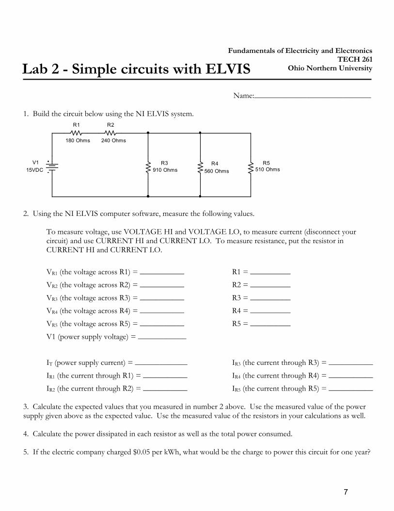
2. The power dissipated in each resistor along with the total power dissipated is as follows. .00335 3.3 0.0111 11.1 .00253 5.5 0.0139 13.9 .000816 5.5 0.00449 4.49 .00335 8.8 0.02948 29.48
3. If the power supply was replaced with a battery with a capacity of 1500mAh its life expectancy is calculated as follows. 1.50.00335 447.76
Conclusion:
The "Measuring Simple Circuits" lab demonstrated the proper measuring methods for DC voltage, current, and resistance with a multimeter. Ohm's law and Kirchhoff's voltage law were also used to verify the measurements. The resistor color code learned in the lecture was utilized to calculate the expected values of the resistors and to verify that the resistors were within their manufacturing tolerance. The power dissipated in each resistor and total power dissipated was calculated along with the life expectancy of a battery utilized to power the given circuit.
29

General guidelines for generating lab reports 1. All equations must be shown first in equation form (with the letters), then with the equivalent values of all the variables in place, then finally with the answers. Look at the example lab in the discussion section for an example. Use appropriate subscripts when necessary. Use the Microsoft equation editor to generate these equations. Search online if you don’t know how to use it or just ask. 2. All circuits that are constructed must be drawn accurately by using an electrical cad package. DO NOT SCAN IN THE LAB HANDOUT AND COPY THE PICTURE. YOU MIGHT AS WELL NOT DO IT AT ALL! There is a free electrical cad program at http://www.expresspcb.com. You can install it on your own computer if you wish. Again, if you have trouble using it, just ask. Please do not use Microsoft Word to “draw” the circuits. I won’t accept the lab report that way. However, any other electrical cad program is sufficient. 3. Each individual should create their own lab report. That means that each individual should draw their own circuit and generate their own equations. Your report should not look exactly the same as someone else in the class, especially your partner! 4. Please don’t copy the abstract, discussion, or conclusion from the example lab report and use it as your own. Not only is that academic dishonesty, but it also won’t suffice for subsequent lab reports as they are different.
30

©2004 Fairchild Semiconductor Corporation Rev. A1, August 2004
Absolute Maximum Ratings * Ta=25°C unless otherwise noted
* These ratings are limiting values above which the serviceability of any semiconductor device may be impaired
NOTES:1) These ratings are based on a maximum junction temperature of 150 degrees C.2) These are steady state limits. The factory should be consulted on applications involving pulsed or low duty cycle operations
Electrical Characteristics Ta=25°C unless otherwise noted
* Pulse Test: Pulse Width ≤ 300µs, Duty Cycle ≤ 2.0%
Symbol Parameter Value UnitsVCEO Collector-Emitter Voltage 40 VVCBO Collector-Base Voltage 75 VVEBO Emitter-Base Voltage 6.0 VIC Collector Current 1.0 ATSTG Operating and Storage Junction Temperature Range - 55 ~ 150 °C
Symbol Parameter Test Condition Min. Max. UnitsOff CharacteristicsBV(BR)CEO Collector-Emitter Breakdown Voltage * IC = 10mA, IB = 0 40 VBV(BR)CBO Collector-Base Breakdown Voltage IC = 10µA, IE = 0 75 VBV(BR)EBO Emitter-Base Breakdown Voltage IE = 10µA, IC = 0 6.0 VICEX Collector Cutoff Current VCE = 60V, VEB(off) = 3.0V 10 nAICBO Collector Cutoff Current VCB = 60V, IE = 0
VCB = 60V, IE = 0, Ta = 125°C0.0110
µAµA
IEBO Emitter Cutoff Current VEB = 3.0V, IC = 0 10 µAIBL Base Cutoff Current VCE = 60V, VEB(off) = 3.0V 20 µAOn CharacteristicshFE DC Current Gain IC = 0.1mA, VCE = 10V
IC = 1.0mA, VCE = 10V IC = 10mA, VCE = 10VIC = 10mA, VCE = 10V, Ta = -55°CIC = 150mA, VCE = 10V *IC = 150mA, VCE = 10V *IC = 500mA, VCE = 10V *
35507535
1005040
300
VCE(sat) Collector-Emitter Saturation Voltage * IC = 150mA, VCE = 10VIC = 500mA, VCE = 10V
0.31.0
VV
VBE(sat) Base-Emitter Saturation Voltage * IC = 150mA, VCE = 10VIC = 500mA, VCE = 10V
0.6 1.22.0
VV
NPN General Purpose Amplifier• This device is for use as a medium power amplifier and switch
requiring collector currents up to 500mA.• Sourced from process 19.
PN2222A MMBT2222A PZT2222A
E B CTO-92 SOT-23 SOT-223
Mark:1P
C
B
EE
BC
C
31

©2004 Fairchild Semiconductor Corporation Rev. A1, August 2004
Electrical Characteristics Ta=25°C unless otherwise noted (Continued)
Thermal Characteristics Ta=25°C unless otherwise noted
* Device mounted on FR-4 PCB 1.6” × 1.6” × 0.06”.** Device mounted on FR-4 PCB 36mm × 18mm × 1.5mm; mounting pad for the collector lead min. 6cm2.
Spice ModelNPN (Is = 14.34f Xti = 3 Eg = 1.11 Vaf = 74.03 Bf = 255.9 Ne = 1.307 Ise = 14.34 Ikf = .2847 Xtb = 1.5 Br = 6.092 Isc = 0Ikr = 0 Rc = 1 Cjc = 7.306p Mjc = .3416 Vjc = .75 Fc = .5 Cje = 22.01p Mje = .377 Vje = .75 Tr = 46.91n Tf = 411.1p Itf = .6Vtf = 1.7 Xtf = 3 Rb = 10)
Symbol Parameter Test Condition Min. Max. UnitsSmall Signal CharacteristicsfT Current Gain Bandwidth Product IC = 20mA, VCE = 20V, f = 100MHz 300 MHzCobo Output Capacitance VCB = 10V, IE = 0, f = 1MHz 8.0 pFCibo Input Capacitance VEB = 0.5V, IC = 0, f = 1MHz 25 pFrb’Cc Collector Base Time Constant IC = 20mA, VCB = 20V, f = 31.8MHz 150 pSNF Noise Figure IC = 100µA, VCE = 10V,
RS = 1.0KΩ, f = 1.0KHz4.0 dB
Re(hie) Real Part of Common-Emitter High Frequency Input Impedance
IC = 20mA, VCE = 20V, f = 300MHz 60 Ω
Switching Characteristicstd Delay Time VCC = 30V, VEB(off) = 0.5V,
IC = 150mA, IB1 = 15mA10 ns
tr Rise Time 25 nsts Storage Time VCC = 30V, IC = 150mA,
IB1 = IB2 = 15mA225 ns
tf Fall Time 60 ns
Symbol ParameterMax.
UnitsPN2222A *MMBT2222A **PZT2222A
PD Total Device DissipationDerate above 25°C
6255.0
3502.8
1,0008.0
mWmW/°C
RθJC Thermal Resistance, Junction to Case 83.3 °C/WRθJA Thermal Resistance, Junction to Ambient 200 357 125 °C/W
32

©2004 Fairchild Semiconductor Corporation Rev. A1, August 2004
Typical Characteristics
Figure 1. Typical Pulsed Current Gainvs Collector Current
Figure 2. Collector-Emitter Saturation Voltagevs Collector Current
Figure 3. Base-Emitter Saturation Voltagevs Collector Current
Figure 4. Base-Emitter On Voltagevs Collector Current
Figure 5. Collector Cutoff Currentvs Ambient Temperature
Figure 6. Emitter Transition and Output Capacitancevs Reverse Bias Voltage
0.1 0.3 1 3 10 30 100 3000
100
200
300
400
500
I - COLLECTOR CURRENT (mA)
h
- T
YP
ICA
L P
ULS
ED
CU
RR
EN
T G
AIN
C
FE
125 °C
25 °C
- 40 °C
V = 5VCE
β
β
1 10 100 500
0.1
0.2
0.3
0.4
I - COLLECTOR CURRENT (mA)V
-
CO
LLEC
TOR
-EM
ITTE
R V
OLT
AG
E (V
)C
ESAT
25 캜캜캜캜
C
ββββ = 10
125 캜캜캜캜
- 40 캜캜캜캜
°C
°C
°C
1 10 100 500
0.4
0.6
0.8
1
I - COLLECTOR CURRENT (mA)
V
-
BA
SE-E
MIT
TER
VO
LTA
GE
(V)
BES
AT
C
ββββ = 10
25 캜캜캜캜
125 캜캜캜캜
- 40 캜캜캜캜°C
°C
°C
IC
β
β
0.1 1 10 250.2
0.4
0.6
0.8
1
I - COLLECTOR CURRENT (mA)V
- B
AS
E-E
MIT
TE
R O
N V
OLT
AG
E (
V)
BE
(ON
)
C
V = 5VCE
25 °C
125 °C
- 40 °C
IC
25 50 75 100 125 150
0.1
1
10
100
500
T - AMBIENT TEMPERATURE ( C)
I
- C
OLL
ECTO
R C
UR
REN
T (n
A)
A
V = 40VCB
CB
O
°
β
β
0.1 1 10 100
4
8
12
16
20
REVERSE BIAS VOLTAGE (V)
CA
PAC
ITA
NC
E (
pF)
f = 1 MHz
C ob
C te
33

©2004 Fairchild Semiconductor Corporation Rev. A1, August 2004
Typical Characteristics
Figure 7. Turn On and Turn Off Timesvs Collector Current
Figure 8. Switching Times vs Collector Current
Figure 9. Power Dissipation vs Ambient Temperature
Figure 10. Common Emitter Characteristics
Figure 11. Common Emitter Characteristics Figure 12. Common Emitter Characteristics
10 100 10000
80
160
240
320
400
I - COLLECTOR CURRENT (mA)
TIM
E (
nS
)
I = I =
t on
t off
B1
C
B2I c
10
V = 25 Vcc
IC10 100 1000
0
80
160
240
320
400
I - COLLECTOR CURRENT (mA)
TIM
E (
nS
)
I = I =
t r
t s
B1
C
B2I c
10
V = 25 Vcc
t f
t d
IC
0 25 50 75 100 125 1500
0.25
0.5
0.75
1
TEMPERATURE ( C)
P -
PO
WER
DIS
SIPA
TIO
N (W
)D
o
SOT-223TO-92
SOT-23
0 10 20 30 40 50 600
2
4
6
8
I - COLLECTOR CURRENT (mA)
CH
AR
. REL
ATIV
E TO
VA
LUES
AT
I =
10m
AV = 10 VCE
C
C T = 25 CA o
hoe
h re
h fe
h ie
0 20 40 60 80 1000
0.4
0.8
1.2
1.6
2
2.4
T - AMBIENT TEMPERATURE ( C)
CH
AR
. REL
ATIV
E TO
VA
LUES
AT
T =
25
C
V = 10 VCE
A
A I = 10 mAC
hoe
hre
hfe
h ie
o
o
0 5 10 15 20 25 30 350.750.8
0.850.9
0.951
1.051.1
1.151.2
1.251.3
V - COLLECTOR VOLTAGE (V)
CH
AR
. REL
ATIV
E TO
VA
LUES
AT
V =
10V
CE
CE T = 25 CA
o
hoe
h re
h fe
h ie
I = 10 mAC
34

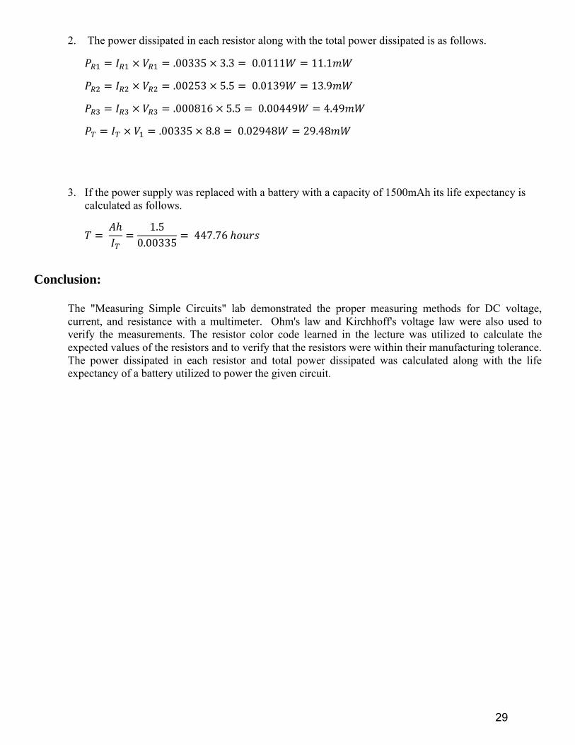
Package Dimensions
TO-92
Dimensions in Millimeters
©2002 Fairchild Semiconductor Corporation Rev. A1, August 2004
35
©2002 Fairchild Semiconductor Corporation Rev. A1, August 2004
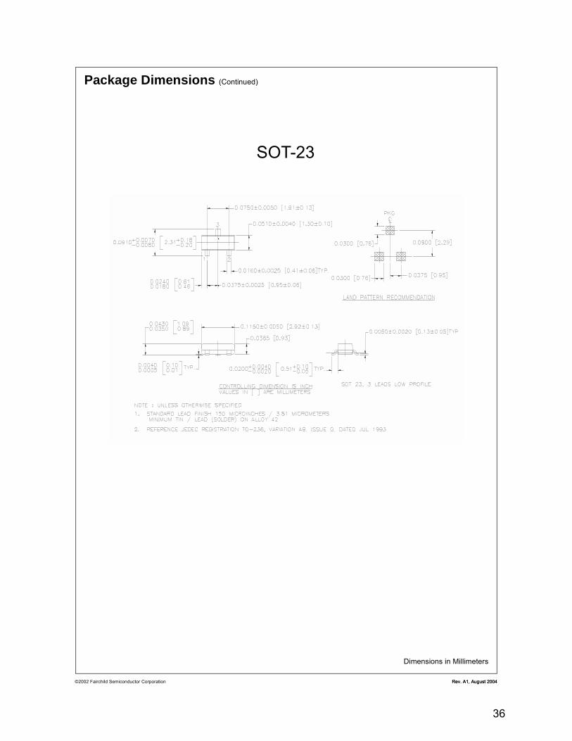
Package Dimensions (Continued)
Dimensions in Millimeters
Rev. A1, August 2004
SOT-23
36

©2002 Fairchild Semiconductor Corporation Rev. A1, August 2004
Package Dimensions (Continued)
Dimensions in Millimeters
Rev. A1, August 2004
SOT-223
37
Rev. I11
TRADEMARKS
The following are registered and unregistered trademarks Fairchild Semiconductor owns or is authorized to use and is notintended to be an exhaustive list of all such trademarks.
DISCLAIMERFAIRCHILD SEMICONDUCTOR RESERVES THE RIGHT TO MAKE CHANGES WITHOUT FURTHER NOTICE TO ANYPRODUCTS HEREIN TO IMPROVE RELIABILITY, FUNCTION OR DESIGN. FAIRCHILD DOES NOT ASSUME ANYLIABILITY ARISING OUT OF THE APPLICATION OR USE OF ANY PRODUCT OR CIRCUIT DESCRIBED HEREIN;NEITHER DOES IT CONVEY ANY LICENSE UNDER ITS PATENT RIGHTS, NOR THE RIGHTS OF OTHERS.
LIFE SUPPORT POLICY
FAIRCHILD’S PRODUCTS ARE NOT AUTHORIZED FOR USE AS CRITICAL COMPONENTS IN LIFE SUPPORTDEVICES OR SYSTEMS WITHOUT THE EXPRESS WRITTEN APPROVAL OF FAIRCHILD SEMICONDUCTORCORPORATION.As used herein:1. Life support devices or systems are devices or systemswhich, (a) are intended for surgical implant into the body,or (b) support or sustain life, or (c) whose failure to performwhen properly used in accordance with instructions for useprovided in the labeling, can be reasonably expected toresult in significant injury to the user.
2. A critical component is any component of a life supportdevice or system whose failure to perform can bereasonably expected to cause the failure of the life supportdevice or system, or to affect its safety or effectiveness.
PRODUCT STATUS DEFINITIONS
Definition of Terms
Datasheet Identification Product Status Definition
Advance Information Formative or In Design
This datasheet contains the design specifications forproduct development. Specifications may change inany manner without notice.
Preliminary First Production This datasheet contains preliminary data, andsupplementary data will be published at a later date.Fairchild Semiconductor reserves the right to makechanges at any time without notice in order to improvedesign.
No Identification Needed Full Production This datasheet contains final specifications. FairchildSemiconductor reserves the right to make changes atany time without notice in order to improve design.
Obsolete Not In Production This datasheet contains specifications on a productthat has been discontinued by Fairchild semiconductor.The datasheet is printed for reference information only.
FAST®
FASTr™FPS™FRFET™GlobalOptoisolator™GTO™HiSeC™I2C™i-Lo™ImpliedDisconnect™
ISOPLANAR™LittleFET™MICROCOUPLER™MicroFET™MicroPak™MICROWIRE™MSX™MSXPro™OCX™OCXPro™OPTOLOGIC®
OPTOPLANAR™PACMAN™POP™
Power247™PowerSaver™PowerTrench®
QFET®
QS™QT Optoelectronics™Quiet Series™RapidConfigure™RapidConnect™µSerDes™SILENT SWITCHER®
SMART START™SPM™Stealth™
SuperFET™SuperSOT™-3SuperSOT™-6SuperSOT™-8SyncFET™TinyLogic®
TINYOPTO™TruTranslation™UHC™UltraFET®
VCX™
ACEx™ActiveArray™Bottomless™CoolFET™CROSSVOLT™DOME™EcoSPARK™E2CMOS™EnSigna™FACT™FACT Quiet Series™Across the board. Around the world.™The Power Franchise®
Programmable Active Droop™
©2004 Fairchild Semiconductor Corporation
38

TL3472HIGH-SLEW-RATE, SINGLE-SUPPLY OPERATIONAL AMPLIFIER
SLOS200G – OCTOBER 1997 – REVISED JULY 2003
1POST OFFICE BOX 655303 • DALLAS, TEXAS 75265
Wide Gain-Bandwidth Product . . . 4 MHz
High Slew Rate . . . 13 V/µs
Fast Settling Time . . . 1.1 µs to 0.1%
Wide-Range Single-SupplyOperation . . . 4 V to 36 V
Wide Input Common-Mode Range IncludesGround (VCC–)
Low Total Harmonic Distortion . . . 0.02%
Large-Capacitance DriveCapability . . . 10,000 pF
Output Short-Circuit Protection
description/ordering information
Quality, low-cost, bipolar fabrication with innovative design concepts is employed for the TL3472 operationalamplifier. This device offers 4 MHz of gain-bandwidth product, 13-V/µs slew rate, and fast settling time, withoutthe use of JFET device technology. Although the TL3472 can be operated from split supplies, it is particularlysuited for single-supply operation because the common-mode input voltage range includes ground potential(VCC–). With a Darlington transistor input stage, this device exhibits high input resistance, low input offsetvoltage, and high gain. The all-npn output stage, characterized by no dead-band crossover distortion and largeoutput voltage swing, provides high-capacitance drive capability, excellent phase and gain margins, lowopen-loop high-frequency output impedance, and symmetrical source/sink ac frequency response. Thislow-cost amplifier is an alternative to the MC33072 and the MC34072 operational amplifiers.
ORDERING INFORMATION
TA PACKAGE† ORDERABLEPART NUMBER
TOP-SIDEMARKING
PDIP (P) Tube of 25 TL3472CP TL3472CP
0°C to 70°CSOIC (D)
Tube of 50 TL3472CD3472CSOIC (D)
Reel of 2500 TL3472CDR3472C
PDIP (P) Tube of 25 TL3472IP TL3472IP
–40°C to 105°CSOIC (D)
Tube of 50 TL3472IDZ3472SOIC (D)
Reel of 2500 TL3472IDRZ3472
† Package drawings, standard packing quantities, thermal data, symbolization, and PCB designguidelines are available at www.ti.com/sc/package.
PRODUCTION DATA information is current as of publication date.Products conform to specifications per the terms of Texas Instrumentsstandard warranty. Production processing does not necessarily includetesting of all parameters.
Copyright 2003, Texas Instruments Incorporated
Please be aware that an important notice concerning availability, standard warranty, and use in critical applications ofTexas Instruments semiconductor products and disclaimers thereto appears at the end of this data sheet.
1
2
3
4
8
7
6
5
1OUT1IN–1IN+
VCC–/GND
VCC+2OUT2IN–2IN+
D OR P PACKAGE(TOP VIEW)
39

TL3472HIGH-SLEW-RATE, SINGLE-SUPPLY OPERATIONAL AMPLIFIER
SLOS200G – OCTOBER 1997 – REVISED JULY 2003
2 POST OFFICE BOX 655303 • DALLAS, TEXAS 75265
schematic (each amplifier)
VCC+
OUT
VCC–/GND
IN–
IN+
40

TL3472HIGH-SLEW-RATE, SINGLE-SUPPLY OPERATIONAL AMPLIFIER
SLOS200G – OCTOBER 1997 – REVISED JULY 2003
3POST OFFICE BOX 655303 • DALLAS, TEXAS 75265
absolute maximum ratings over operating free-air temperature range (unless otherwise noted)†
Supply voltage (see Note 1): VCC+ 18 V. . . . . . . . . . . . . . . . . . . . . . . . . . . . . . . . . . . . . . . . . . . . . . . . . . . . . . . . . . VCC– –18 V. . . . . . . . . . . . . . . . . . . . . . . . . . . . . . . . . . . . . . . . . . . . . . . . . . . . . . . . .
Differential input voltage, VID (see Note 2) ±36 V. . . . . . . . . . . . . . . . . . . . . . . . . . . . . . . . . . . . . . . . . . . . . . . . . . . Input voltage, VI (any input) VCC±. . . . . . . . . . . . . . . . . . . . . . . . . . . . . . . . . . . . . . . . . . . . . . . . . . . . . . . . . . . . . . . . Input current, II (each input) ±1 mA. . . . . . . . . . . . . . . . . . . . . . . . . . . . . . . . . . . . . . . . . . . . . . . . . . . . . . . . . . . . . . . Output current, IO ±80 mA. . . . . . . . . . . . . . . . . . . . . . . . . . . . . . . . . . . . . . . . . . . . . . . . . . . . . . . . . . . . . . . . . . . . . . . Total current into VCC+ 80 mA. . . . . . . . . . . . . . . . . . . . . . . . . . . . . . . . . . . . . . . . . . . . . . . . . . . . . . . . . . . . . . . . . . . Total current out of VCC– 80 mA. . . . . . . . . . . . . . . . . . . . . . . . . . . . . . . . . . . . . . . . . . . . . . . . . . . . . . . . . . . . . . . . . . Duration of short-circuit current at (or below) 25°C (see Note 3) Unlimited. . . . . . . . . . . . . . . . . . . . . . . . . . . . . . Package thermal impedance, θJA (see Notes 4 and 5): D package 97°C/W. . . . . . . . . . . . . . . . . . . . . . . . . . . .
P package 85°C/W. . . . . . . . . . . . . . . . . . . . . . . . . . . . Operating virtual junction temperature, TJ 150°C. . . . . . . . . . . . . . . . . . . . . . . . . . . . . . . . . . . . . . . . . . . . . . . . . . . Lead temperature 1.6 mm (1/16 inch) from case for 10 seconds 260°C. . . . . . . . . . . . . . . . . . . . . . . . . . . . . . . Storage temperature range, Tstg –65°C to 150°C. . . . . . . . . . . . . . . . . . . . . . . . . . . . . . . . . . . . . . . . . . . . . . . . . . .
† Stresses beyond those listed under “absolute maximum ratings” may cause permanent damage to the device. These are stress ratings only, andfunctional operation of the device at these or any other conditions beyond those indicated under “recommended operating conditions” is notimplied. Exposure to absolute-maximum-rated conditions for extended periods may affect device reliability.
NOTES: 1. All voltage values, except differential voltages, are with respect to the midpoint between VCC+ and VCC–.2. Differential voltages are at the noninverting input with respect to the inverting input. Excessive input current can flow when the input
is less than VCC– – 0.3 V.3. The output can be shorted to either supply. Temperature and/or supply voltages must be limited to ensure that the maximum
dissipation rating is not exceeded.4. Maximum power dissipation is a function of TJ(max), θJA, and TA. The maximum allowable power dissipation at any allowable
ambient temperature is PD = (TJ(max) – TA)/θJA. Operating at the absolute maximum TJ of 150°C can impact reliability.5. The package thermal impedance is calculated in accordance with JESD 51-7.
recommended operating conditions
MIN MAX UNIT
VCC± Supply voltage 4 36 V
VIC Common mode input voltageVCC = 5 V 0 2.8
VVIC Common-mode input voltageVCC± = ±15 V –15 12.8
V
TA Operating free air temperatureTL3472C 0 70
°CTA Operating free-air temperatureTL3472I –40 105
°C
41

TL3472HIGH-SLEW-RATE, SINGLE-SUPPLY OPERATIONAL AMPLIFIER
SLOS200G – OCTOBER 1997 – REVISED JULY 2003
4 POST OFFICE BOX 655303 • DALLAS, TEXAS 75265
electrical characteristics at specified free-air temperature, VCC± = ±15 V (unless otherwise noted)
PARAMETER TEST CONDITIONS TA MIN TYP† MAX UNIT
VCC = 5 V 25°C 1.5 10
VIO Input offset voltageVCC = ±15 V
25°C 1.0 10 mVVCC = ±15 V
Full range‡ 12
VIO
Temperature coefficient ofinput offset voltage
VIC = 0,VO = 0,
VCC = ±15 V Full range‡ 10 µV/°C
IIO Input offset current
ORS = 50 Ω
VCC = ±15 V25°C 6 75
nAIIO Input offset current VCC = ±15 VFull range‡ 300
nA
IIB Input bias current VCC = ±15 V25°C 100 500
nAIIB Input bias current VCC = ±15 VFull range‡ 700
nA
VICRCommon-mode
RS = 50 Ω
25°C–15
to12.8
VVICR input voltage rangeRS = 50 Ω
Full range‡–15
to12.8
V
VCC+ = 5 V, VCC– = 0, RL = 2 kΩ 25°C 3.7 4
VOH High-level output voltage RL = 10 kΩ 25°C 13.6 14 V
RL = 2 kΩ Full range‡ 13.4
VCC+ = 5 V, VCC– = 0, RL = 2 kΩ 25°C 0.1 0.3
VOL Low-level output voltage RL = 10 kΩ 25°C –14.7 –14.3 V
RL = 2 kΩ Full range‡ –13.5
AVDLarge-signal differential
VO = ±10 V RL = 2 kΩ25°C 25 100
V/mVAVDg g
voltage amplificationVO = ±10 V, RL = 2 kΩ
Full range‡ 20V/mV
IOS Short circuit output currentSource: VID = 1 V, VO = 0
25°C–10 –34
mAIOS Short-circuit output currentSink: VID = –1 V, VO = 0
25°C20 27
mA
CMRR Common mode rejection ratio VIC = VICR(min) RS = 50 Ω 25°C 65 97 dBCMRR Common-mode rejection ratio VIC = VICR(min), RS = 50 Ω 25°C 65 97 dB
kSVRSupply-voltage rejection ratio(∆VCC±/∆VIO)
VCC± = ±13.5 V to ±16.5 V, RS = 100 Ω 25°C 70 97 dB
VO = 0 No load25°C 3.5 4.5
ICC Supply current (per channel)VO = 0, No load
Full range‡ 4.5 5.5 mA
VCC+ = 5 V, VO = 2.5 V, VCC– = 0, No load 25°C 3.5 4.5
† All typical values are at TA = 25°C.‡ Full range is 0°C to 70°C for the TL3472C device and –40°C to 105°C for the TL3472I device.
42
TL3472HIGH-SLEW-RATE, SINGLE-SUPPLY OPERATIONAL AMPLIFIER
SLOS200G – OCTOBER 1997 – REVISED JULY 2003
5POST OFFICE BOX 655303 • DALLAS, TEXAS 75265
operating characteristics, VCC± = ±15 V, TA = 25°CPARAMETER TEST CONDITIONS MIN TYP MAX UNIT
SR+ Positive slew rate VI = –10 V to 10 V, AV = 1 8 10 V/µs
SR– Negative slew rateI ,
RL = 2 kΩ, CL = 300 pF AV = –1 13 V/µs
t Settling time AVD = 1 10 V stepTo 0.1% 1.1
µsts Settling time AVD = –1, 10-V stepTo 0.01% 2.2
µs
Vn Equivalent input noise voltage f = 1 kHz, RS = 100 Ω 49 nV/√Hz
In Equivalent input noise current f = 1 kHz 0.22 pA/√Hz
THD Total harmonic distortion VO(PP) = 2 V to 20 V, RL = 2 kΩ, AVD = 10, f = 10 kHz 0.02 %
GBW Gain-bandwidth product f =100 kHz 3 4 MHz
BW Power bandwidth VO(PP) 20 V RL 2 kΩ AVD 1 THD 5 0% 160 kHzBW Power bandwidth VO(PP) = 20 V, RL = 2 kΩ, AVD = 1, THD = 5.0% 160 kHz
φ Phase margin RL = 2 kΩCL = 0 70
degφm Phase margin RL = 2 kΩCL = 300 pF 50
deg
Gain margin RL = 2 kΩCL = 0 12
dBGain margin RL = 2 kΩCL = 300 pF 4
dB
ri Differential input resistance VIC = 0 150 MΩ
Ci Input capacitance VIC = 0 2.5 pF
Channel separation f = 10 kHz 101 dB
zo Open-loop output impedance f = 1 MHz, AV = 1 20 Ω
43

PACKAGING INFORMATION
Orderable Device Status (1) PackageType
PackageDrawing
Pins PackageQty
Eco Plan (2) Lead/Ball Finish MSL Peak Temp (3)
TL3472CD ACTIVE SOIC D 8 75 Green (RoHS &no Sb/Br)
CU NIPDAU Level-2-260C-1YEAR
TL3472CDE4 ACTIVE SOIC D 8 75 Green (RoHS &no Sb/Br)
CU NIPDAU Level-2-260C-1YEAR
TL3472CDG4 ACTIVE SOIC D 8 75 Green (RoHS &no Sb/Br)
CU NIPDAU Level-2-260C-1YEAR
TL3472CDR ACTIVE SOIC D 8 2500 Green (RoHS &no Sb/Br)
CU NIPDAU Level-2-260C-1YEAR
TL3472CDRE4 ACTIVE SOIC D 8 2500 Green (RoHS &no Sb/Br)
CU NIPDAU Level-2-260C-1YEAR
TL3472CDRG4 ACTIVE SOIC D 8 2500 Green (RoHS &no Sb/Br)
CU NIPDAU Level-2-260C-1YEAR
TL3472CP ACTIVE PDIP P 8 50 Pb-Free(RoHS)
CU NIPDAU N / A for Pkg Type
TL3472CPE4 ACTIVE PDIP P 8 50 Pb-Free(RoHS)
CU NIPDAU N / A for Pkg Type
TL3472ID ACTIVE SOIC D 8 75 Green (RoHS &no Sb/Br)
CU NIPDAU Level-2-260C-1YEAR
TL3472IDE4 ACTIVE SOIC D 8 75 Green (RoHS &no Sb/Br)
CU NIPDAU Level-2-260C-1YEAR
TL3472IDR ACTIVE SOIC D 8 2500 Green (RoHS &no Sb/Br)
CU NIPDAU Level-2-260C-1YEAR
TL3472IDRE4 ACTIVE SOIC D 8 2500 Green (RoHS &no Sb/Br)
CU NIPDAU Level-2-260C-1YEAR
TL3472IP ACTIVE PDIP P 8 50 Pb-Free(RoHS)
CU NIPDAU N / A for Pkg Type
TL3472IPE4 ACTIVE PDIP P 8 50 Pb-Free(RoHS)
CU NIPDAU N / A for Pkg Type
(1) The marketing status values are defined as follows:ACTIVE: Product device recommended for new designs.LIFEBUY: TI has announced that the device will be discontinued, and a lifetime-buy period is in effect.NRND: Not recommended for new designs. Device is in production to support existing customers, but TI does not recommend using this part ina new design.PREVIEW: Device has been announced but is not in production. Samples may or may not be available.OBSOLETE: TI has discontinued the production of the device.
(2) Eco Plan - The planned eco-friendly classification: Pb-Free (RoHS), Pb-Free (RoHS Exempt), or Green (RoHS & no Sb/Br) - please checkhttp://www.ti.com/productcontent for the latest availability information and additional product content details.TBD: The Pb-Free/Green conversion plan has not been defined.Pb-Free (RoHS): TI's terms "Lead-Free" or "Pb-Free" mean semiconductor products that are compatible with the current RoHS requirementsfor all 6 substances, including the requirement that lead not exceed 0.1% by weight in homogeneous materials. Where designed to be solderedat high temperatures, TI Pb-Free products are suitable for use in specified lead-free processes.Pb-Free (RoHS Exempt): This component has a RoHS exemption for either 1) lead-based flip-chip solder bumps used between the die andpackage, or 2) lead-based die adhesive used between the die and leadframe. The component is otherwise considered Pb-Free (RoHScompatible) as defined above.Green (RoHS & no Sb/Br): TI defines "Green" to mean Pb-Free (RoHS compatible), and free of Bromine (Br) and Antimony (Sb) based flameretardants (Br or Sb do not exceed 0.1% by weight in homogeneous material)
(3) MSL, Peak Temp. -- The Moisture Sensitivity Level rating according to the JEDEC industry standard classifications, and peak soldertemperature.
Important Information and Disclaimer:The information provided on this page represents TI's knowledge and belief as of the date that it is
PACKAGE OPTION ADDENDUM
www.ti.com 12-Jan-2006
Addendum-Page 1
44

provided. TI bases its knowledge and belief on information provided by third parties, and makes no representation or warranty as to theaccuracy of such information. Efforts are underway to better integrate information from third parties. TI has taken and continues to takereasonable steps to provide representative and accurate information but may not have conducted destructive testing or chemical analysis onincoming materials and chemicals. TI and TI suppliers consider certain information to be proprietary, and thus CAS numbers and other limitedinformation may not be available for release.
In no event shall TI's liability arising out of such information exceed the total purchase price of the TI part(s) at issue in this document sold by TIto Customer on an annual basis.
PACKAGE OPTION ADDENDUM
www.ti.com 12-Jan-2006
Addendum-Page 2
45

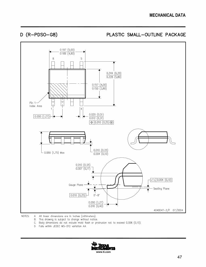
MECHANICAL DATA
MPDI001A – JANUARY 1995 – REVISED JUNE 1999
POST OFFICE BOX 655303 • DALLAS, TEXAS 75265
P (R-PDIP-T8) PLASTIC DUAL-IN-LINE
8
4
0.015 (0,38)
Gage Plane
0.325 (8,26)0.300 (7,62)
0.010 (0,25) NOM
MAX0.430 (10,92)
4040082/D 05/98
0.200 (5,08) MAX
0.125 (3,18) MIN
5
0.355 (9,02)
0.020 (0,51) MIN
0.070 (1,78) MAX
0.240 (6,10)0.260 (6,60)
0.400 (10,60)
1
0.015 (0,38)0.021 (0,53)
Seating Plane
M0.010 (0,25)
0.100 (2,54)
NOTES: A. All linear dimensions are in inches (millimeters).B. This drawing is subject to change without notice.C. Falls within JEDEC MS-001
For the latest package information, go to http://www.ti.com/sc/docs/package/pkg_info.htm
46
47

IMPORTANT NOTICE
Texas Instruments Incorporated and its subsidiaries (TI) reserve the right to make corrections, modifications,enhancements, improvements, and other changes to its products and services at any time and to discontinueany product or service without notice. Customers should obtain the latest relevant information before placingorders and should verify that such information is current and complete. All products are sold subject to TI’s termsand conditions of sale supplied at the time of order acknowledgment.
TI warrants performance of its hardware products to the specifications applicable at the time of sale inaccordance with TI’s standard warranty. Testing and other quality control techniques are used to the extent TIdeems necessary to support this warranty. Except where mandated by government requirements, testing of allparameters of each product is not necessarily performed.
TI assumes no liability for applications assistance or customer product design. Customers are responsible fortheir products and applications using TI components. To minimize the risks associated with customer productsand applications, customers should provide adequate design and operating safeguards.
TI does not warrant or represent that any license, either express or implied, is granted under any TI patent right,copyright, mask work right, or other TI intellectual property right relating to any combination, machine, or processin which TI products or services are used. Information published by TI regarding third-party products or servicesdoes not constitute a license from TI to use such products or services or a warranty or endorsement thereof.Use of such information may require a license from a third party under the patents or other intellectual propertyof the third party, or a license from TI under the patents or other intellectual property of TI.
Reproduction of information in TI data books or data sheets is permissible only if reproduction is withoutalteration and is accompanied by all associated warranties, conditions, limitations, and notices. Reproductionof this information with alteration is an unfair and deceptive business practice. TI is not responsible or liable forsuch altered documentation.
Resale of TI products or services with statements different from or beyond the parameters stated by TI for thatproduct or service voids all express and any implied warranties for the associated TI product or service andis an unfair and deceptive business practice. TI is not responsible or liable for any such statements.
Following are URLs where you can obtain information on other Texas Instruments products and applicationsolutions:
Products Applications
Amplifiers amplifier.ti.com Audio www.ti.com/audio
Data Converters dataconverter.ti.com Automotive www.ti.com/automotive
DSP dsp.ti.com Broadband www.ti.com/broadband
Interface interface.ti.com Digital Control www.ti.com/digitalcontrol
Logic logic.ti.com Military www.ti.com/military
Power Mgmt power.ti.com Optical Networking www.ti.com/opticalnetwork
Microcontrollers microcontroller.ti.com Security www.ti.com/security
Telephony www.ti.com/telephony
Video & Imaging www.ti.com/video
Wireless www.ti.com/wireless
Mailing Address: Texas Instruments
Post Office Box 655303 Dallas, Texas 75265
Copyright 2006, Texas Instruments Incorporated
48