Embed Size (px)
Citation preview
User’s Manual
HOW TO USE DDR SDRAM
Document No. E0234E50 (Ver.5.0) Date Published August 2007 (K) Japan Printed in Japan URL: http://www.elpida.com © Elpida Memory, Inc. 2002-2007

User’s Manual E0234E50 (Ver.5.0) 3
Descriptions in this document are provided only for illustrative purpose in semiconductor product operation and application
examples. Use these information under the full responsibility of the customer. For details about the functions of individual products,
refer to the corresponding data sheet.
INTRODUCTION
This manual is intended for users who design application systems using double data rate synchronous
DRAM (DDR SDRAM). Readers of this manual are required to have general knowledge in the fields of
electrical engineering, logic circuits, as well as detailed knowledge of the functions and usage of
conventional synchronous DRAM (SDRAM).
Conventions Caution: Information requiring particular attention
Note: Footnote for items marked with Note in the text
Remark: Supplementary information
Related Documents
Related documents indicated in this manual may include preliminary versions, but they may not be
explicitly marked as preliminary.
Document Name Document Number
HOW TO USE SDRAM USER’S MANUAL E0123N
Notice This dicument is intended to give users understanding of basic functions and usage of DDR2 SDRAM.
Descriptions in this document are provided only for illustrative purpose in semiconductor product operation
and application examples. And numerical values are not guaranteed values. For details about the functions
of individual products, refer to the corresponding data sheet. The incorporation of these information in the
design of the customer’s equipment shall be done under the full responsibility of the customer. Elpida
Memory, Inc. assumes no responsibility for any losses incurred by customers or third parties arising from
the use of these information.
User’s Manual E0234E50 (Ver.5.0) 4
Descriptions in this document are provided only for illustrative purpose in semiconductor product operation and application
examples. Use these information under the full responsibility of the customer. For details about the functions of individual products,
refer to the corresponding data sheet.
CONTENTS CHAPTER 1 DIFFERENCES BETWEEN SDRAM AND DDR SDRAM..............................................................10
1.1 Differences in Functions and Specifications ....................................................................................................11 1.1.1 Data transfer frequency, data rate ............................................................................................................12 1.1.2 Clock input ................................................................................................................................................13 1.1.3 Data strobe signal (DQS)..........................................................................................................................13 1.1.4 Interface....................................................................................................................................................14 1.1.5 Power supply ............................................................................................................................................15 1.1.6 /CAS read latency, /CAS write latency, burst length, and burst sequence................................................15 1.1.7 Use of DLL................................................................................................................................................15 1.1.8 Data mask.................................................................................................................................................15
1.2 Differences in Commands ...............................................................................................................................16 1.2.1 Clock suspend ..........................................................................................................................................16 1.2.2 Full-page burst..........................................................................................................................................16 1.2.3 Burst stop .................................................................................................................................................16 1.2.4 Single write after burst read ......................................................................................................................16
1.3 Differences in Operation Timing ......................................................................................................................17 CHAPTER 2 PRODUCT OUTLINE ........................................................................................................................19
2.1 Pin Configurations ...........................................................................................................................................19 2.2 Pin Functions...................................................................................................................................................21
2.2.1 Clock input (CK, /CK)................................................................................................................................21 2.2.2 Clock enable input (CKE)..........................................................................................................................21 2.2.3 Chip select input (/CS)..............................................................................................................................21 2.2.4 Row address strobe input (/RAS), Column address strobe input (/CAS), Write enable input (/WE) .........21 2.2.5 Address input (A0 to Ax) ...........................................................................................................................22 2.2.6 Bank Address input (BA0, BA1)................................................................................................................22 2.2.7 Data input/output (DQ0 to DQx)................................................................................................................23 2.2.8 Data strobe input/output (DQS, LDQS, UDQS) ........................................................................................23 2.2.9 DQ write mask enable input (DM, LDM, UDM) .........................................................................................23 2.2.10 Power supply (for the internal circuit) (VDD, VSS)..................................................................................23 2.2.11 Power supply (for DQ) (VDDQ, VSSQ)...................................................................................................23 2.2.12 Referential voltage (VREF) .....................................................................................................................23
2.3 Block Diagram.................................................................................................................................................24 2.3.1 Memory cell array of 128M bit DDR SDRAM ............................................................................................25 2.3.2 Address decoder (Row address decoder, Column address decoder) .......................................................26 2.3.3 I/O buffer...................................................................................................................................................26 2.3.4 Refresh counter ........................................................................................................................................26 2.3.5 DLL (Delay Locked Loop) .........................................................................................................................26
User’s Manual E0234E50 (Ver.5.0) 5
Descriptions in this document are provided only for illustrative purpose in semiconductor product operation and application
examples. Use these information under the full responsibility of the customer. For details about the functions of individual products,
refer to the corresponding data sheet.
CHAPTER 3 PRODUCT FEATURES.....................................................................................................................27 3.1 Synchronous Operation...................................................................................................................................28 3.2 Command Control ...........................................................................................................................................29
3.2.1 Command input timing..............................................................................................................................29 3.2.2 DDR SDRAM command table...................................................................................................................30
3.3 MultiBank Operation........................................................................................................................................31 3.3.1 Four-bank configuration ............................................................................................................................31 3.3.2 Multibank operations.................................................................................................................................32
3.4 Burst Operation ...............................................................................................................................................33 3.5 Access Time....................................................................................................................................................35
CHAPTER 4 INITIALIZATION .................................................................................................................................38
4.1 Initialization after Power On.............................................................................................................................38 CHAPTER 5 MODE REGISTER SET....................................................................................................................40
5.1 Programming the Mode Register.....................................................................................................................40 5.2 Parameters......................................................................................................................................................40 5.3 Mode Register and Extended Mode Register Fields .......................................................................................45
CHAPTER 6 SIMPLIFIED STATE DIAGRAM .......................................................................................................46
6.1 Simplified State Diagram of DDR SDRAM ......................................................................................................46 6.2 Current State Definition ...................................................................................................................................48
6.2.1 Idle (IDLE).................................................................................................................................................48 6.2.2 Bank activating (Row activating) ...............................................................................................................48 6.2.3 Bank active (BANK ACTIVE) (Row active) ...............................................................................................48 6.2.4 Precharging ..............................................................................................................................................48 6.2.5 Read and write (READ, WRIT) .................................................................................................................48 6.2.6 Read and write with auto precharge (READA, WRITA) ............................................................................48 6.2.7 Mode register set ......................................................................................................................................48 6.2.8 CBR (Auto) refresh ...................................................................................................................................48 6.2.9 Self refresh ...............................................................................................................................................49 6.2.10 Self refresh recovery...............................................................................................................................49 6.2.11 Power down ............................................................................................................................................49
CHAPTER 7 COMMAND OPERATIONS ...............................................................................................................50
7.1 DDR SDRAM Command Truth Table..............................................................................................................50 7.2 Command Execution Conditions .....................................................................................................................51 7.3 Command Operation of DDR SDRAM ............................................................................................................52
CHAPTER 8 BASIC OPERATION MODES...........................................................................................................58
8.1 Read Mode......................................................................................................................................................58 8.2 tRAS Lockout Function (Fast Auto Precharge)................................................................................................61 8.3 Write Mode......................................................................................................................................................62 8.4 Refresh Mode..................................................................................................................................................64
User’s Manual E0234E50 (Ver.5.0) 6
Descriptions in this document are provided only for illustrative purpose in semiconductor product operation and application
examples. Use these information under the full responsibility of the customer. For details about the functions of individual products,
refer to the corresponding data sheet.
CHAPTER 9 DATA STROBE SIGNAL (DQS) CONTROL OPERATION............................................................65 9.1 Data Strobe Signal (DQS) ...............................................................................................................................65
9.1.1 Data strobe signal (DQS) in read cycle.....................................................................................................66 9.1.2 Data strobe signal (DQS) in write cycle ....................................................................................................67
9.2 Relationship between Data Strobe Signal (DQS) / Output Data (DQ) and Clock (CK, /CK)
during Read Cycle ...........................................................................................................................................68 9.3 Relationship between Data Strobe Signal (DQS) and Output Data (DQ) in Read Cycle .................................69 9.4 Data Strobe Signal (DQS) Read Preamble and Read Postamble ...................................................................70 9.5 Relationship between Data Strobe Signal (DQS) and Input Data (DQ) /
DQ Write Mask Enable Signal (DM) during Write Cycle ..................................................................................72 9.6 Data Strobe Signal (DQS) Write Preamble and Write Postamble ...................................................................73
CHAPTER 10 DQ WRITE MASK ENABLE SIGNAL (DM) CONTROL OPERATION.......................................74
10.1 DQ Write Mask Enable Signal (DM) ..............................................................................................................74 10.2 DQ Write Mask Enable Signal (DM) Control in Write Cycle...........................................................................75 10.3 DQ Write Mask Enable Signal (DM) Truth Table...........................................................................................75
CHAPTER 11 CLOCK ENABLE SIGNAL (CKE) CONTROL OPERATION........................................................76
11.1 Basic Control .................................................................................................................................................76 11.2 Example of Clock Enable Signal (CKE) Control ............................................................................................77
11.2.1 Power down mode ..................................................................................................................................78 11.2.2 Self refresh mode ...................................................................................................................................79 11.2.3 Clock enable signal (CKE) command truth table.....................................................................................80
CHAPTER 12 BURST OPERATION ......................................................................................................................82
12.1 Terminating Burst Operation .........................................................................................................................82 12.1.1 Data interrupt by read command.............................................................................................................82 12.1.2 Data interrupt by write command ............................................................................................................84 12.1.3 Ending burst operation by burst stop command......................................................................................86 12.1.4 Terminating burst operation by precharge command..............................................................................87
User’s Manual E0234E50 (Ver.5.0) 7
Descriptions in this document are provided only for illustrative purpose in semiconductor product operation and application
examples. Use these information under the full responsibility of the customer. For details about the functions of individual products,
refer to the corresponding data sheet.
LIST OF FIGURES (1/2)
Figure No. Title Page
Figure 1-1. 2-Bit Prefetch Architecture.......................................................................................................................12 Figure 1-2. Clock Input...............................................................................................................................................13 Figure 1-3. SSTL_2 Interface (case of DIMM) ...........................................................................................................14 Figure 1-4. DDR SDRAM Read Cycle Timing............................................................................................................17 Figure 1-5. SDR SDRAM Read Cycle Timing............................................................................................................17 Figure 1-6. DDR SDRAM Write Cycle Timing............................................................................................................18 Figure 1-7. SDR SDRAM Write Cycle Timing ............................................................................................................18
Figure 2-1. Pin Configuration of 128M bit DDR SDRAM............................................................................................19 Figure 2-2. Pin Configuration of 256M/512M bit DDR SDRAM..................................................................................20 Figure 2-3. Block Diagram of 128M bit DDR SDRAM................................................................................................24 Figure 2-4. Memory Cell Array of 128M bit DDR SDRAM (Bank A)...........................................................................25
Figure 3-1. DDR SDRAM Read Cycle Timing............................................................................................................28 Figure 3-2. DDR SDRAM Write Cycle Timing............................................................................................................28 Figure 3-3. Command Input Timing ...........................................................................................................................29 Figure 3-4. Four-Bank Configuration..........................................................................................................................31 Figure 3-5. Burst Operation .......................................................................................................................................34 Figure 3-6. Burst Read Cycle.....................................................................................................................................36 Figure 3-7. Access Time of DDR SDRAM, SDR SDRAM and EDO DRAM...............................................................37
Figure 4-1. Initializing DDR SDRAM ..........................................................................................................................39
Figure 5-1. Mode Register/Extended Mode Register Set Cycle.................................................................................40 Figure 5-2. Read/Write Cycle with Burst Length of 8 .................................................................................................41 Figure 5-3. Burst Sequence .......................................................................................................................................42 Figure 5-4. Timing Differences between /CAS Latency = 2 and 2.5...........................................................................44 Figure 5-5. Mode Register and Extended Mode Register fields (with 128M bit DDR SDRAM)..................................45
Figure 6-1. Simplified State Diagram of DDR SDRAM...............................................................................................47
Figure 8-1. Read Cycle ..............................................................................................................................................59 Figure 8-2. Read Cycle with Auto Precharge .............................................................................................................60 Figure 8-3. Read with Auto Precharge (Fast Auto Precharge supported) (Example of DDR266) ..............................61 Figure 8-4. Write Cycle ..............................................................................................................................................62 Figure 8-5. Write Cycle with Auto Precharge .............................................................................................................63 Figure 8-6. CBR (Auto) Refresh Cycle.......................................................................................................................64
User’s Manual E0234E50 (Ver.5.0) 8
Descriptions in this document are provided only for illustrative purpose in semiconductor product operation and application
examples. Use these information under the full responsibility of the customer. For details about the functions of individual products,
refer to the corresponding data sheet.
LIST OF FIGURES (2/2)
Figure No. Title Page
Figure 9-1. Relationship between Data Strobe Signal and Data Input/Output ...........................................................65 Figure 9-2. Data Strobe Signal in Read Cycle ...........................................................................................................66 Figure 9-3. Data Strobe Signal in Write Cycle............................................................................................................67 Figure 9-4. Data Strobe Signal and Output Data Timing as Related to Clock in Read Cycle.....................................68 Figure 9-5. Data Strobe Signal and Output Data in Read Cycle ................................................................................69 Figure 9-6. Timing of Data Strobe Signal Read Preamble and Read Postamble 1....................................................71 Figure 9-7. Timing of Data Strobe Signal Read Preamble and Read Postamble 2 (Read-to-Read Data Bus transition) ........................................................................................................71 Figure 9-8. Timing Parameters of DQ/DM during Write Cycle ...................................................................................72 Figure 9-9. Timing of Data Strobe Signal Write Preamble and Write Postamble .......................................................73
Figure 10-1. DQ Write Mask Enable Signal Control during Write Cycle.....................................................................75
Figure 11-1. Signal Input Timing Controlled by Clock Enable Signal .........................................................................76 Figure 11-2. Example of Clock Enable Signal Control ...............................................................................................77 Figure 11-3. Power Down Mode ................................................................................................................................78 Figure 11-4. Self Refresh Mode.................................................................................................................................79
Figure 12-1. Read/Read Command ...........................................................................................................................82 Figure 12-2. Write/Read Command ...........................................................................................................................83 Figure 12-3. Write/Write Command ...........................................................................................................................84 Figure 12-4. Read/Burst Stop/Write Command .........................................................................................................85 Figure 12-5. Read/Burst Stop Command...................................................................................................................86 Figure 12-6. Read/Precharge Command ...................................................................................................................87 Figure 12-7. Write/Precharge Command ...................................................................................................................88
User’s Manual E0234E50 (Ver.5.0) 9
Descriptions in this document are provided only for illustrative purpose in semiconductor product operation and application
examples. Use these information under the full responsibility of the customer. For details about the functions of individual products,
refer to the corresponding data sheet.
LIST OF TABLES
Table No. Title Page
Table 1-1. Differences in Functions and Specifications .............................................................................................11 Table 1-2. SSTL_2 Interface Specifications...............................................................................................................15 Table 1-3. Differences in Commands.........................................................................................................................16
Table 2-1. Address Pins of 128M bit DDR SDRAM ...................................................................................................22 Table 2-2. Bank Address and Selected Bank ............................................................................................................22
Table 3-1. DDR SDRAM (×4/×8/×16-bit Organization) Command List.......................................................................30 Table 3-2. Access Time of DDR SDRAM, SDR SDRAM and EDO DRAM................................................................37
Table 7-1. DDR SDRAM (×4/×8/×16-bit Organization) Command Truth Table..........................................................50 Table 7-2. Command Executable Condition...............................................................................................................51
Table 9-1. AC Characteristics of Data Strobe Signal and Output Data in Read Cycle...............................................68 Table 9-2. AC Characteristics of Data Strobe Signal and Output Data in Read Cycle...............................................69 Table 9-3. AC Characteristics of Data Strobe Signal Read Preamble and Read Postamble .....................................70 Table 9-4. AC Characteristics of DQ/DM in Write Cycle ............................................................................................72 Table 9-5. AC Characteristics of Data Strobe Signal Write Preamble and Write Postamble .....................................73
Table 10-1. DQ Write Mask Enable Signal Truth Table .............................................................................................75
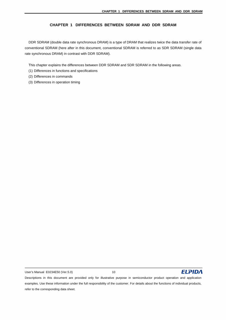
CHAPTER 1 DIFFERENCES BETWEEN SDRAM AND DDR SDRAM
User’s Manual E0234E50 (Ver.5.0) 10
Descriptions in this document are provided only for illustrative purpose in semiconductor product operation and application
examples. Use these information under the full responsibility of the customer. For details about the functions of individual products,
refer to the corresponding data sheet.
CHAPTER 1 DIFFERENCES BETWEEN SDRAM AND DDR SDRAM
DDR SDRAM (double data rate synchronous DRAM) is a type of DRAM that realizes twice the data transfer rate of
conventional SDRAM (here after in this document, conventional SDRAM is referred to as SDR SDRAM (single data
rate synchronous DRAM) in contrast with DDR SDRAM).
This chapter explains the differences between DDR SDRAM and SDR SDRAM in the following areas.
(1) Differences in functions and specifications
(2) Differences in commands
(3) Differences in operation timing
CHAPTER 1 DIFFERENCES BETWEEN SDRAM AND DDR SDRAM
User’s Manual E0234E50 (Ver.5.0) 11
Descriptions in this document are provided only for illustrative purpose in semiconductor product operation and application
examples. Use these information under the full responsibility of the customer. For details about the functions of individual products,
refer to the corresponding data sheet.
1.1 Differences in Functions and Specifications
DDR SDRAM is a type of SDRAM that inherits technologies from SDR SDRAM and realizes faster operation and
lower power consumption. It shares many common aspects with SDR SDRAM, which enables easy transition to
DDR SDRAM.
This section explains the differences in functions and specifications between DDR SDRAM and SDR SDRAM.
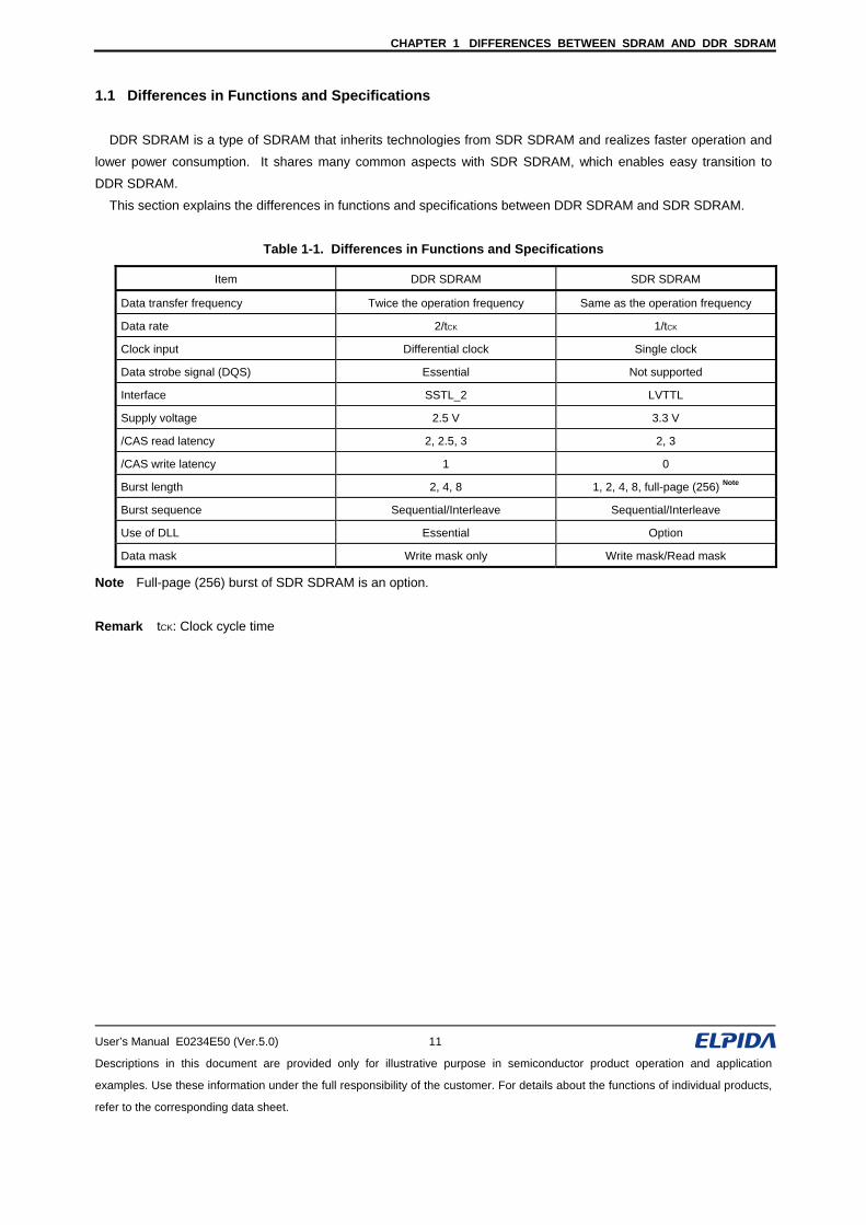
Table 1-1. Differences in Functions and Specifications
Item DDR SDRAM SDR SDRAM
Data transfer frequency Twice the operation frequency Same as the operation frequency
Data rate 2/tCK 1/tCK
Clock input Differential clock Single clock
Data strobe signal (DQS) Essential Not supported
Interface SSTL_2 LVTTL
Supply voltage 2.5 V 3.3 V
/CAS read latency 2, 2.5, 3 2, 3
/CAS write latency 1 0
Burst length 2, 4, 8 1, 2, 4, 8, full-page (256) Note
Burst sequence Sequential/Interleave Sequential/Interleave
Use of DLL Essential Option
Data mask Write mask only Write mask/Read mask
Note Full-page (256) burst of SDR SDRAM is an option.
Remark tCK: Clock cycle time
CHAPTER 1 DIFFERENCES BETWEEN SDRAM AND DDR SDRAM
User’s Manual E0234E50 (Ver.5.0) 12
Descriptions in this document are provided only for illustrative purpose in semiconductor product operation and application
examples. Use these information under the full responsibility of the customer. For details about the functions of individual products,
refer to the corresponding data sheet.
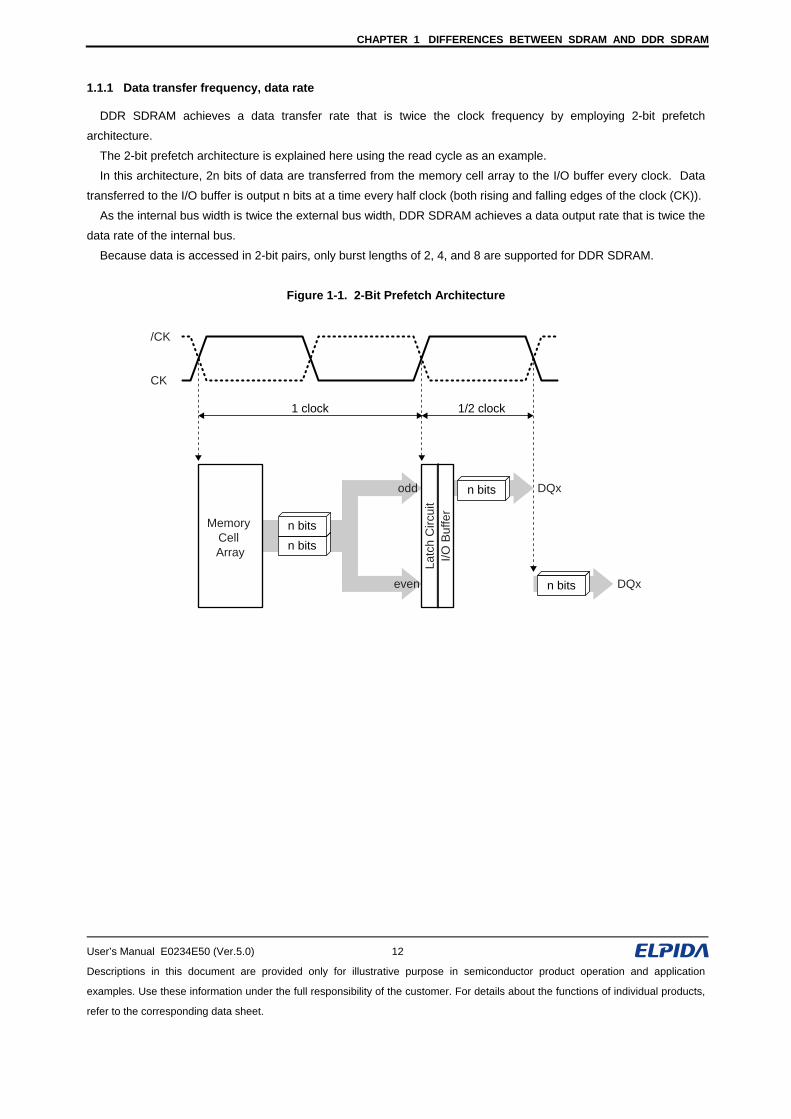
1.1.1 Data transfer frequency, data rate
DDR SDRAM achieves a data transfer rate that is twice the clock frequency by employing 2-bit prefetch
architecture.
The 2-bit prefetch architecture is explained here using the read cycle as an example.
In this architecture, 2n bits of data are transferred from the memory cell array to the I/O buffer every clock. Data
transferred to the I/O buffer is output n bits at a time every half clock (both rising and falling edges of the clock (CK)).
As the internal bus width is twice the external bus width, DDR SDRAM achieves a data output rate that is twice the
data rate of the internal bus.
Because data is accessed in 2-bit pairs, only burst lengths of 2, 4, and 8 are supported for DDR SDRAM.
Figure 1-1. 2-Bit Prefetch Architecture
Memory Cell Array
Latc
h C
ircui
tI/O
Buf
fer
DQx
DQxodd
even
CK
/CK
1 clock 1/2 clock
n bits
n bits
n bits
n bits
CHAPTER 1 DIFFERENCES BETWEEN SDRAM AND DDR SDRAM
User’s Manual E0234E50 (Ver.5.0) 13
Descriptions in this document are provided only for illustrative purpose in semiconductor product operation and application
examples. Use these information under the full responsibility of the customer. For details about the functions of individual products,
refer to the corresponding data sheet.
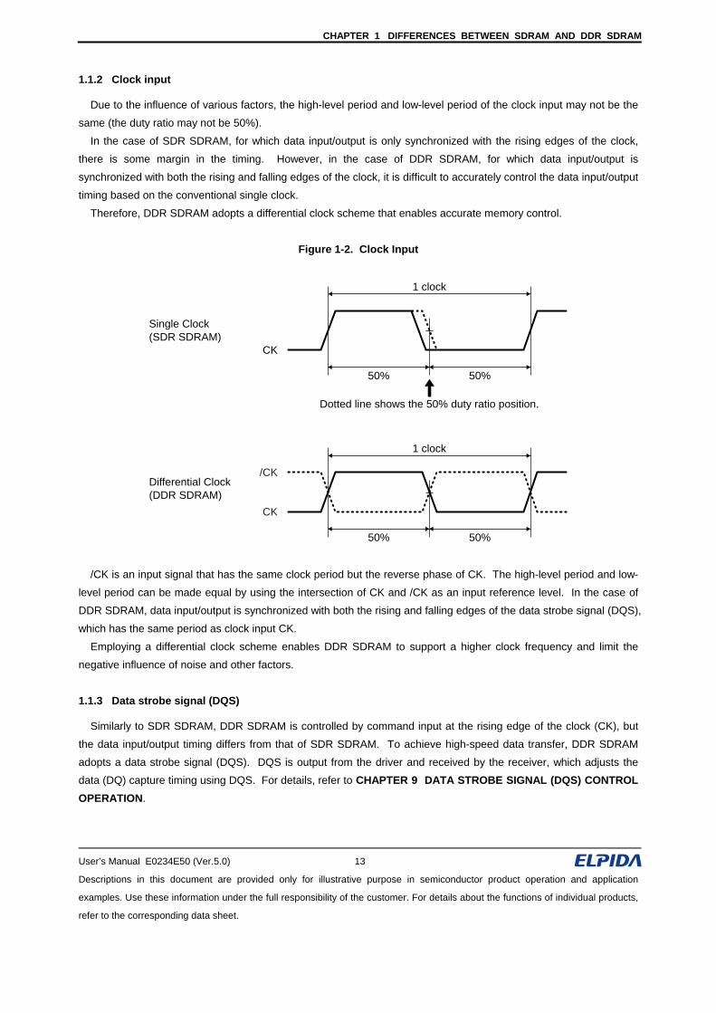
1.1.2 Clock input
Due to the influence of various factors, the high-level period and low-level period of the clock input may not be the
same (the duty ratio may not be 50%).
In the case of SDR SDRAM, for which data input/output is only synchronized with the rising edges of the clock,
there is some margin in the timing. However, in the case of DDR SDRAM, for which data input/output is
synchronized with both the rising and falling edges of the clock, it is difficult to accurately control the data input/output
timing based on the conventional single clock.
Therefore, DDR SDRAM adopts a differential clock scheme that enables accurate memory control.
Figure 1-2. Clock Input
Single Clock(SDR SDRAM)
Differential Clock(DDR SDRAM)
1 clock
50% 50%
Dotted line shows the 50% duty ratio position.
CK
1 clock
50% 50%
CK
/CK
/CK is an input signal that has the same clock period but the reverse phase of CK. The high-level period and low-
level period can be made equal by using the intersection of CK and /CK as an input reference level. In the case of
DDR SDRAM, data input/output is synchronized with both the rising and falling edges of the data strobe signal (DQS),
which has the same period as clock input CK.
Employing a differential clock scheme enables DDR SDRAM to support a higher clock frequency and limit the
negative influence of noise and other factors.
1.1.3 Data strobe signal (DQS)
Similarly to SDR SDRAM, DDR SDRAM is controlled by command input at the rising edge of the clock (CK), but
the data input/output timing differs from that of SDR SDRAM. To achieve high-speed data transfer, DDR SDRAM
adopts a data strobe signal (DQS). DQS is output from the driver and received by the receiver, which adjusts the data (DQ) capture timing using DQS. For details, refer to CHAPTER 9 DATA STROBE SIGNAL (DQS) CONTROL OPERATION.
CHAPTER 1 DIFFERENCES BETWEEN SDRAM AND DDR SDRAM
User’s Manual E0234E50 (Ver.5.0) 14
Descriptions in this document are provided only for illustrative purpose in semiconductor product operation and application
examples. Use these information under the full responsibility of the customer. For details about the functions of individual products,
refer to the corresponding data sheet.
1.1.4 Interface
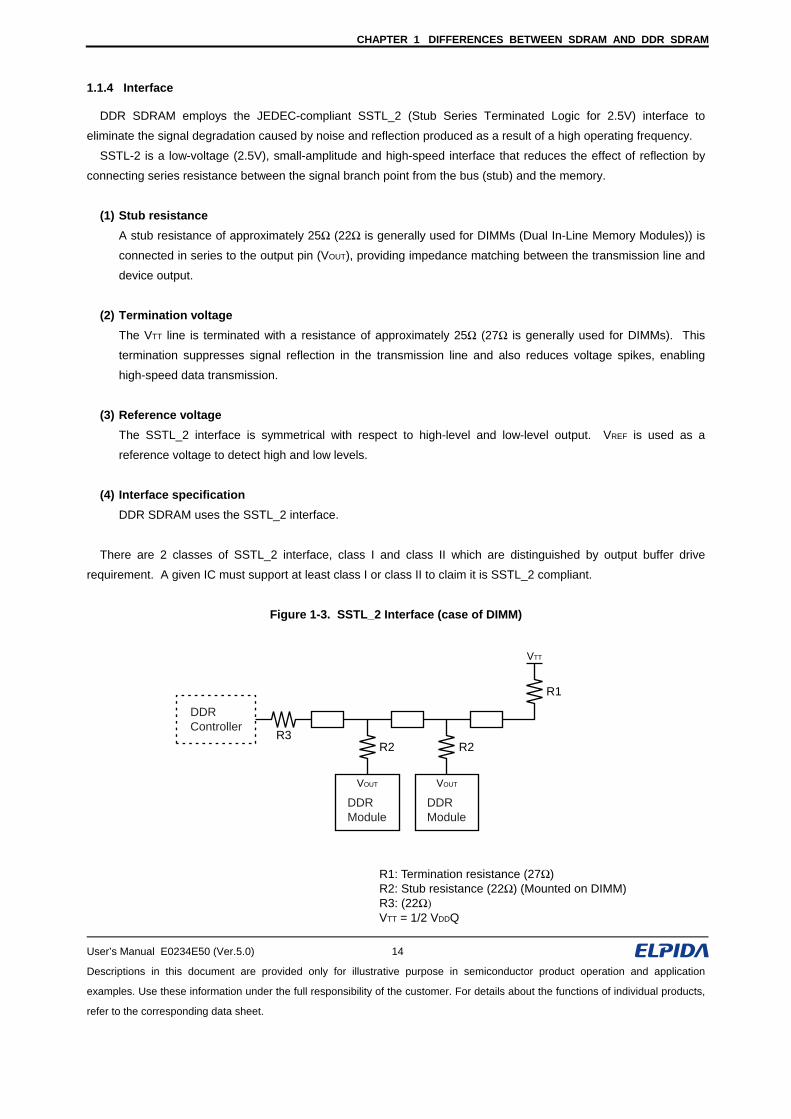
DDR SDRAM employs the JEDEC-compliant SSTL_2 (Stub Series Terminated Logic for 2.5V) interface to
eliminate the signal degradation caused by noise and reflection produced as a result of a high operating frequency.
SSTL-2 is a low-voltage (2.5V), small-amplitude and high-speed interface that reduces the effect of reflection by
connecting series resistance between the signal branch point from the bus (stub) and the memory.
(1) Stub resistance
A stub resistance of approximately 25Ω (22Ω is generally used for DIMMs (Dual In-Line Memory Modules)) is
connected in series to the output pin (VOUT), providing impedance matching between the transmission line and
device output.
(2) Termination voltage
The VTT line is terminated with a resistance of approximately 25Ω (27Ω is generally used for DIMMs). This
termination suppresses signal reflection in the transmission line and also reduces voltage spikes, enabling
high-speed data transmission.
(3) Reference voltage
The SSTL_2 interface is symmetrical with respect to high-level and low-level output. VREF is used as a
reference voltage to detect high and low levels.
(4) Interface specification
DDR SDRAM uses the SSTL_2 interface.
There are 2 classes of SSTL_2 interface, class I and class II which are distinguished by output buffer drive
requirement. A given IC must support at least class I or class II to claim it is SSTL_2 compliant.
Figure 1-3. SSTL_2 Interface (case of DIMM)
DDR Controller
R1: Termination resistance (27Ω)R2: Stub resistance (22Ω) (Mounted on DIMM) R3: (22Ω)VTT = 1/2 VDDQ
R2R3
R2
R1
VTT
VOUT
DDRModule
VOUT
DDRModule
CHAPTER 1 DIFFERENCES BETWEEN SDRAM AND DDR SDRAM
User’s Manual E0234E50 (Ver.5.0) 15
Descriptions in this document are provided only for illustrative purpose in semiconductor product operation and application
examples. Use these information under the full responsibility of the customer. For details about the functions of individual products,
refer to the corresponding data sheet.
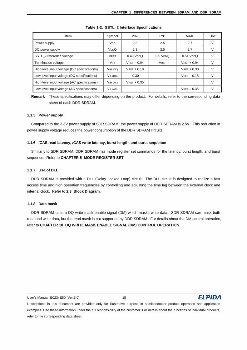
Table 1-2. SSTL_2 Interface Specifications
Item Symbol MIN. TYP. MAX. Unit
Power supply VDD 2.3 2.5 2.7 V
DQ power supply VDDQ 2.3 2.5 2.7 V
SSTL_2 reference voltage VREF 0.49 VDDQ 0.5 VDDQ 0.51 VDDQ V
Termination voltage VTT VREF – 0.04 VREF VREF + 0.04 V
High-level input voltage (DC specifications) VIH (DC) VREF + 0.18 VREF + 0.30 V
Low-level input voltage (DC specifications) VIL (DC) -0.30 VREF – 0.18 V
High-level input voltage (AC specifications) VIH (AC) VREF + 0.35 V
Low-level input voltage (AC specifications) VIL (AC) VREF – 0.35 V
Remark These specifications may differ depending on the product. For details, refer to the corresponding data
sheet of each DDR SDRAM.
1.1.5 Power supply
Compared to the 3.3V power supply of SDR SDRAM, the power supply of DDR SDRAM is 2.5V. This reduction in
power supply voltage reduces the power consumption of the DDR SDRAM circuits.
1.1.6 /CAS read latency, /CAS write latency, burst length, and burst sequence
Similarly to SDR SDRAM, DDR SDRAM has mode register set commands for the latency, burst length, and burst sequence. Refer to CHAPTER 5 MODE REGISTER SET.
1.1.7 Use of DLL
DDR SDRAM is provided with a DLL (Delay Locked Loop) circuit. The DLL circuit is designed to realize a fast
access time and high operation frequencies by controlling and adjusting the time lag between the external clock and internal clock. Refer to 2.3 Block Diagram.
1.1.8 Data mask
DDR SDRAM uses a DQ write mask enable signal (DM) which masks write data. SDR SDRAM can mask both
read and write data, but the read mask is not supported by DDR SDRAM. For details about the DM control operation, refer to CHAPTER 10 DQ WRITE MASK ENABLE SIGNAL (DM) CONTROL OPERATION.
CHAPTER 1 DIFFERENCES BETWEEN SDRAM AND DDR SDRAM
User’s Manual E0234E50 (Ver.5.0) 16
Descriptions in this document are provided only for illustrative purpose in semiconductor product operation and application
examples. Use these information under the full responsibility of the customer. For details about the functions of individual products,
refer to the corresponding data sheet.
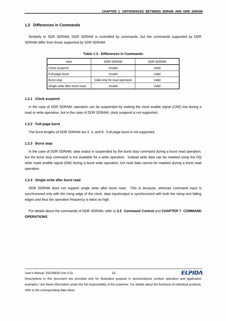
1.2 Differences in Commands
Similarly to SDR SDRAM, DDR SDRAM is controlled by commands, but the commands supported by DDR
SDRAM differ from those supported by SDR SDRAM.
Table 1-3. Differences in Commands
Item DDR SDRAM SDR SDRAM
Clock suspend Invalid Valid
Full-page burst Invalid Valid
Burst stop Valid only for read operation Valid
Single write after burst read Invalid Valid
1.2.1 Clock suspend
In the case of SDR SDRAM, operation can be suspended by making the clock enable signal (CKE) low during a
read or write operation, but in the case of DDR SDRAM, clock suspend is not supported.
1.2.2 Full-page burst
The burst lengths of DDR SDRAM are 2, 4, and 8. Full-page burst is not supported.
1.2.3 Burst stop
In the case of DDR SDRAM, data output is suspended by the burst stop command during a burst read operation,
but the burst stop command is not available for a write operation. Instead write data can be masked using the DQ
write mask enable signal (DM) during a burst write operation, but read data cannot be masked during a burst read
operation.
1.2.4 Single write after burst read
DDR SDRAM does not support single write after burst read. This is because, whereas command input is
synchronized only with the rising edge of the clock, data input/output is synchronized with both the rising and falling
edges and thus the operation frequency is twice as high.
For details about the commands of DDR SDRAM, refer to 3.2 Command Control and CHAPTER 7 COMMAND OPERATIONS.
CHAPTER 1 DIFFERENCES BETWEEN SDRAM AND DDR SDRAM
User’s Manual E0234E50 (Ver.5.0) 17
Descriptions in this document are provided only for illustrative purpose in semiconductor product operation and application
examples. Use these information under the full responsibility of the customer. For details about the functions of individual products,
refer to the corresponding data sheet.
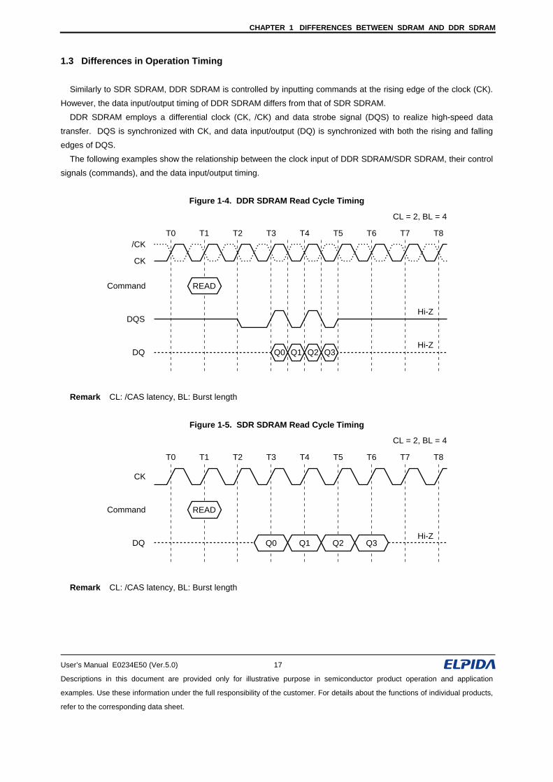
1.3 Differences in Operation Timing
Similarly to SDR SDRAM, DDR SDRAM is controlled by inputting commands at the rising edge of the clock (CK).
However, the data input/output timing of DDR SDRAM differs from that of SDR SDRAM.
DDR SDRAM employs a differential clock (CK, /CK) and data strobe signal (DQS) to realize high-speed data
transfer. DQS is synchronized with CK, and data input/output (DQ) is synchronized with both the rising and falling
edges of DQS.
The following examples show the relationship between the clock input of DDR SDRAM/SDR SDRAM, their control
signals (commands), and the data input/output timing.
Figure 1-4. DDR SDRAM Read Cycle Timing
/CK
Command
DQS
CL = 2, BL = 4
Hi-Z
READ
DQHi-Z
CK
T0 T1 T2 T3 T4 T5 T6 T7 T8
Q0 Q1 Q2 Q3
Remark CL: /CAS latency, BL: Burst length
Figure 1-5. SDR SDRAM Read Cycle Timing
CK
Command
DQ
CL = 2, BL = 4
T0 T1 T2 T3 T4 T5 T6 T7 T8
Hi-Z
READ
Q0 Q1 Q2 Q3
Remark CL: /CAS latency, BL: Burst length
CHAPTER 1 DIFFERENCES BETWEEN SDRAM AND DDR SDRAM
User’s Manual E0234E50 (Ver.5.0) 18
Descriptions in this document are provided only for illustrative purpose in semiconductor product operation and application
examples. Use these information under the full responsibility of the customer. For details about the functions of individual products,
refer to the corresponding data sheet.
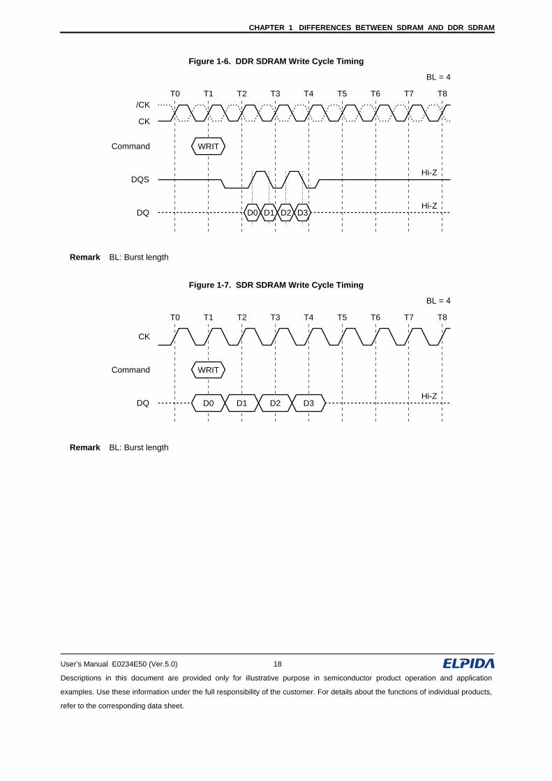
Figure 1-6. DDR SDRAM Write Cycle Timing
/CK
Command
DQS
BL = 4
Hi-Z
WRIT
DQHi-Z
CK
T0 T1 T2 T3 T4 T5 T6 T7 T8
D0 D1 D2 D3
Remark BL: Burst length
Figure 1-7. SDR SDRAM Write Cycle Timing
CK
Command
DQ
BL = 4
T0 T1 T2 T3 T4 T5 T6 T7 T8
Hi-Z
WRIT
D0 D1 D2 D3
Remark BL: Burst length
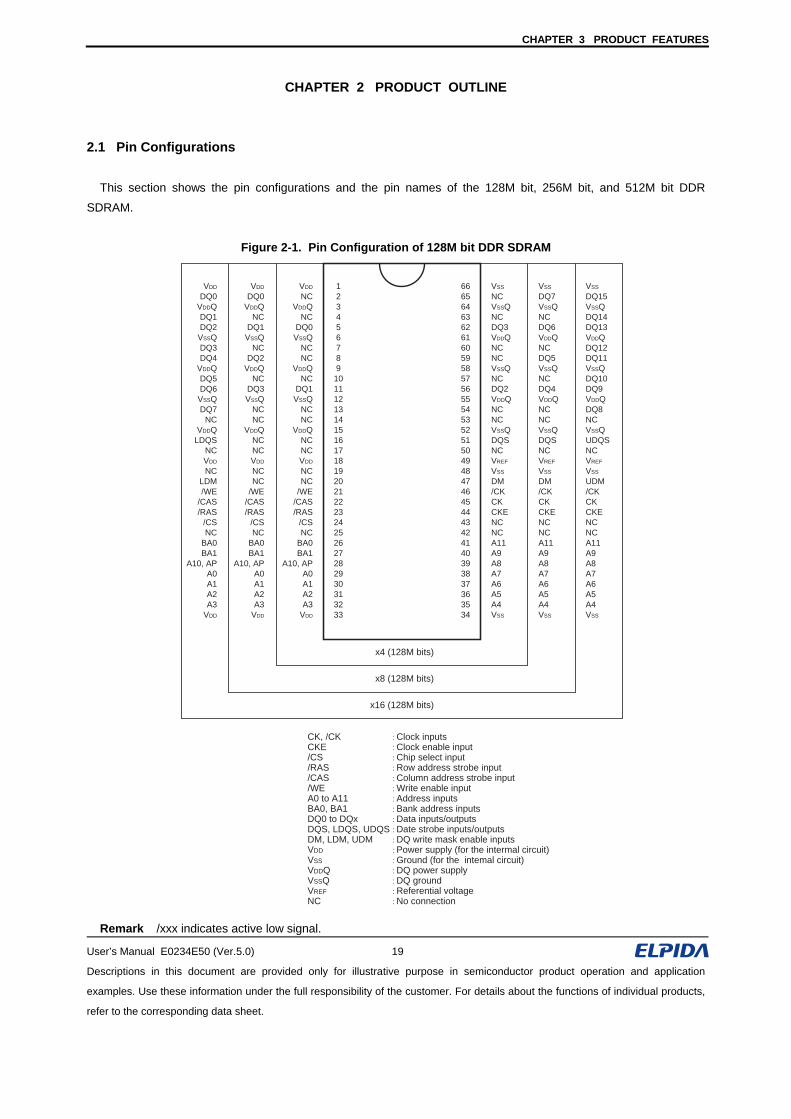
CHAPTER 3 PRODUCT FEATURES
User’s Manual E0234E50 (Ver.5.0) 19
Descriptions in this document are provided only for illustrative purpose in semiconductor product operation and application
examples. Use these information under the full responsibility of the customer. For details about the functions of individual products,
refer to the corresponding data sheet.
CHAPTER 2 PRODUCT OUTLINE
2.1 Pin Configurations
This section shows the pin configurations and the pin names of the 128M bit, 256M bit, and 512M bit DDR
SDRAM.
Figure 2-1. Pin Configuration of 128M bit DDR SDRAM
VDD
NCVDDQ
NCDQ0VSSQ
NCNC
VDDQNC
DQ1VSSQ
NCNC
VDDQNCNCVDD
NCNC
/WE/CAS/RAS
/CSNC
BA0BA1
A10, APA0A1A2A3
VDD
1 2 3 4 5 6 7 8 9101112131415161718192021222324252627282930313233
666564636261605958575655545352515049484746454443424140393837363534
VSS
NCVSSQNCDQ3VDDQNCNCVSSQNCDQ2VDDQNCNCVSSQDQSNCVREF
VSS
DM/CKCKCKENCNCA11A9A8A7A6A5A4VSS
VDD
DQ0VDDQ
NCDQ1VSSQ
NCDQ2
VDDQNC
DQ3VSSQ
NCNC
VDDQNCNCVDD
NCNC
/WE/CAS/RAS
/CSNC
BA0BA1
A10, APA0A1A2A3
VDD
VSS
DQ7VSSQNCDQ6VDDQNCDQ5VSSQNCDQ4VDDQNCNCVSSQDQSNCVREF
VSS
DM/CKCKCKENCNCA11A9A8A7A6A5A4VSS
VDD
DQ0VDDQDQ1DQ2VSSQDQ3DQ4
VDDQDQ5DQ6VSSQDQ7
NCVDDQ
LDQSNCVDD
NCLDM/WE
/CAS/RAS
/CSNC
BA0BA1
A10, APA0A1A2A3
VDD
VSS
DQ15VSSQDQ14DQ13VDDQDQ12DQ11VSSQDQ10DQ9VDDQDQ8NCVSSQUDQSNCVREF
VSS
UDM/CKCKCKENCNCA11A9A8A7A6A5A4VSS
x4 (128M bits)
x8 (128M bits)
x16 (128M bits)
CK, /CK : Clock inputsCKE : Clock enable input/CS : Chip select input/RAS : Row address strobe input/CAS : Column address strobe input/WE : Write enable inputA0 to A11 : Address inputsBA0, BA1 : Bank address inputsDQ0 to DQx : Data inputs/outputsDQS, LDQS, UDQS : Date strobe inputs/outputsDM, LDM, UDM : DQ write mask enable inputsVDD : Power supply (for the intermal circuit)VSS : Ground (for the intemal circuit)VDDQ : DQ power supplyVSSQ : DQ groundVREF : Referential voltageNC : No connection
Remark /xxx indicates active low signal.
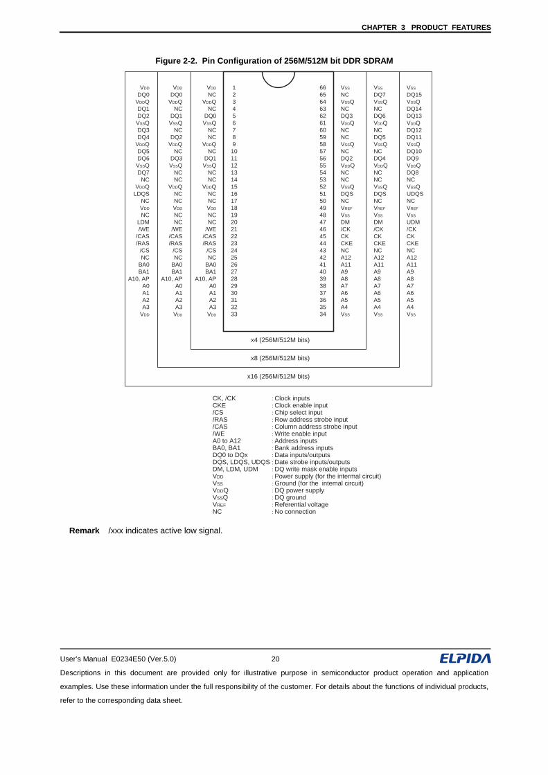
CHAPTER 3 PRODUCT FEATURES
User’s Manual E0234E50 (Ver.5.0) 20
Descriptions in this document are provided only for illustrative purpose in semiconductor product operation and application
examples. Use these information under the full responsibility of the customer. For details about the functions of individual products,
refer to the corresponding data sheet.
Figure 2-2. Pin Configuration of 256M/512M bit DDR SDRAM
VDD
NCVDDQ
NCDQ0
VSSQNCNC
VDDQNC
DQ1VSSQ
NCNC
VDDQNCNCVDD
NCNC
/WE/CAS/RAS
/CSNC
BA0BA1
A10, APA0A1A2A3
VDD
1 2 3 4 5 6 7 8 9101112131415161718192021222324252627282930313233
666564636261605958575655545352515049484746454443424140393837363534
VSS
NCVSSQNCDQ3VDDQNCNCVSSQNCDQ2VDDQNCNCVSSQDQSNCVREF
VSS
DM/CKCKCKENCA12A11A9A8A7A6A5A4VSS
VDD
DQ0VDDQ
NCDQ1
VSSQNC
DQ2VDDQ
NCDQ3VSSQ
NCNC
VDDQNCNCVDD
NCNC
/WE/CAS/RAS
/CSNC
BA0BA1
A10, APA0A1A2A3
VDD
VSS
DQ7VSSQNCDQ6VDDQNCDQ5VSSQNCDQ4VDDQNCNCVSSQDQSNCVREF
VSS
DM/CKCKCKENCA12A11A9A8A7A6A5A4VSS
VDD
DQ0VDDQDQ1DQ2
VSSQDQ3DQ4
VDDQDQ5DQ6
VSSQDQ7
NCVDDQ
LDQSNCVDD
NCLDM/WE
/CAS/RAS
/CSNC
BA0BA1
A10, APA0A1A2A3
VDD
VSS
DQ15VSSQDQ14DQ13VDDQDQ12DQ11VSSQDQ10DQ9VDDQDQ8NCVSSQUDQSNCVREF
VSS
UDM/CKCKCKENCA12A11A9A8A7A6A5A4VSS
x4 (256M/512M bits)
x8 (256M/512M bits)
x16 (256M/512M bits)
CK, /CK : Clock inputsCKE : Clock enable input/CS : Chip select input/RAS : Row address strobe input/CAS : Column address strobe input/WE : Write enable inputA0 to A12 : Address inputsBA0, BA1 : Bank address inputsDQ0 to DQx : Data inputs/outputsDQS, LDQS, UDQS : Date strobe inputs/outputsDM, LDM, UDM : DQ write mask enable inputsVDD : Power supply (for the intermal circuit)VSS : Ground (for the intemal circuit)VDDQ : DQ power supplyVSSQ : DQ groundVREF : Referential voltageNC : No connection
Remark /xxx indicates active low signal.
CHAPTER 3 PRODUCT FEATURES
User’s Manual E0234E50 (Ver.5.0) 21
Descriptions in this document are provided only for illustrative purpose in semiconductor product operation and application
examples. Use these information under the full responsibility of the customer. For details about the functions of individual products,
refer to the corresponding data sheet.
2.2 Pin Functions
This section explains the pin functions of DDR SDRAM.
2.2.1 Clock input (CK, /CK)
Clock input (CK, /CK) for memory operation. /CK has the same period but the reverse phase of CK.
All input signals except data input/output (DQ), data strobe (DQS), and DQ write mask enable (DM), are
synchronized with the rising edge of CK. The intersection of CK and /CK is used as the reference timing for
input/output.
2.2.2 Clock enable input (CKE)
The clock enable signal (CKE) determines whether the clock (CK) is valid or not. If CKE is high at the rising edge
of a given CK, the next rising edge of CK is valid. Otherwise, the next rising edge of CK is invalid.
(1) Self refresh mode
When the device is in the idle state, self refresh mode is set by issuing the self refresh command (CKE is low). In this mode, CKE must be kept low. For details about self refresh mode control by CKE, refer to 11.2.3 Clock enable signal (CKE) command truth table.
(2) Power down mode
When the device is in the idle or bank active state, power down mode is set by setting CKE low. In this mode,
CKE must be kept low. As refresh is not performed automatically in power down mode, the power down mode
period needs to be shorter than the device refresh cycle. For details about power down mode control by CKE, refer to 11.2.3 Clock enable signal (CKE) command truth table.
2.2.3 Chip select input (/CS)
When the chip select (/CS) is low, command input is valid.
When /CS is high, commands are ignored but the operation continues.
2.2.4 Row address strobe input (/RAS), Column address strobe input (/CAS), Write enable input (/WE)
The row address strobe (/RAS), column address strobe (/CAS), and write enable (/WE) functions are same as
those used for SDR SDRAM. Each combination of /RAS, /CAS and /WE in conjunction with chip select (/CS) at the rising edge of the clock (CK) determines the DDR SDRAM operation. For details, refer to 7.1 DDR SDRAM Command Truth Table.
CHAPTER 3 PRODUCT FEATURES
User’s Manual E0234E50 (Ver.5.0) 22
Descriptions in this document are provided only for illustrative purpose in semiconductor product operation and application
examples. Use these information under the full responsibility of the customer. For details about the functions of individual products,
refer to the corresponding data sheet.
2.2.5 Address input (A0 to Ax)
(1) Row address
Determined by addresses (A0 to Ax) when an active command is issued.
(2) Column address
Determined by addresses (A0 to Ax) when a read or write command is issued.
(3) Precharge mode select address (AP)
The function differs depending on the input level of the precharge mode select pin (AP) when a precharge or
read/write command is issued.
When precharge command is issued
AP Function
High level Precharge all banks.
Low level Precharge only one bank selected by bank addresses (BA0, BA1).
When read/write command is issued
AP Function
High level Auto precharge after read/write burst.
Low level Precharge command is necessary to start precharge.
Table 2-1. Address Pins of 128M bit DDR SDRAM
Organization Address Row Column AP
(words x bits x banks) Pins Address Address
8M x 4 x 4 A0 - A11 A0 - A11 A0 - A9, A11 A10
4M x 8 x 4 A0 - A11 A0 - A11 A0 - A9 A10
2M x 16 x 4 A0 - A11 A0 - A11 A0 - A8 A10
2.2.6 Bank Address input (BA0, BA1)
The bank to be selected differs depending on the input level of the bank addresses (BA0, BA1) when a command
is input. Read/write or precharge is applied to the bank selected by BA0 and BA1.
Table 2-2. Bank Address and Selected Bank
Selected Bank BA0 BA1
Bank A L L
Bank B H L
Bank C L H
Bank D H H
CHAPTER 3 PRODUCT FEATURES
User’s Manual E0234E50 (Ver.5.0) 23
Descriptions in this document are provided only for illustrative purpose in semiconductor product operation and application
examples. Use these information under the full responsibility of the customer. For details about the functions of individual products,
refer to the corresponding data sheet.
2.2.7 Data input/output (DQ0 to DQx)
The data input/output (DQ0 to DQx) functions are the same as those used for SDR SDRAM.
2.2.8 Data strobe input/output (DQS, LDQS, UDQS)
Data strobe signals (DQS, LDQS, UDQS) are used to control the I/O buffer. All data input/outputs are
synchronized with the rising and falling edges of these signals. x16-bit products use LDQS and UDQS for the lower
byte and upper byte respectively.
2.2.9 DQ write mask enable input (DM, LDM, UDM)
DQ write mask enable signals (DM, LDM, UDM) mask write data at both the rising and falling edges of the data
strobe signal (DQS). For x16-bit products, LDM and UDM are used to control the lower byte and upper byte
respectively.
If DM is high during a write operation, write data is masked. Unlike the DQ mask enable signal used for SDR
SDRAM, these signals are not used to control read operations.
2.2.10 Power supply (for the internal circuit) (VDD, VSS)
VDD and VSS are power supply pins for the internal circuit.
2.2.11 Power supply (for DQ) (VDDQ, VSSQ)
VDDQ and VSSQ are power supply pins for the I/O buffer.
2.2.12 Referential voltage (VREF)
VREF is the reference voltage supply pin for the SSTL_2 interface.
CHAPTER 3 PRODUCT FEATURES
User’s Manual E0234E50 (Ver.5.0) 24
Descriptions in this document are provided only for illustrative purpose in semiconductor product operation and application
examples. Use these information under the full responsibility of the customer. For details about the functions of individual products,
refer to the corresponding data sheet.
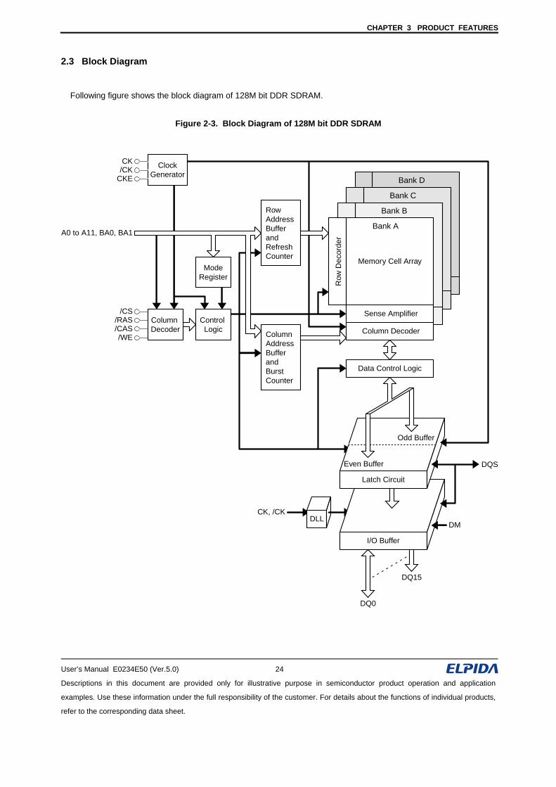
2.3 Block Diagram
Following figure shows the block diagram of 128M bit DDR SDRAM.
Figure 2-3. Block Diagram of 128M bit DDR SDRAM
DLL
I/O Buffer
Control Logic
Data Control Logic
DQS
DQ0
DQ15
CK, /CK
/CS
/WE/CAS/RAS
Bank D
Bank C
Bank B
Memory Cell Array
Row
Dec
orde
rColumn Decoder
Sense Amplifier
Bank A
ClockGenerator
CK
CKE/CK
Odd Buffer
Even Buffer
Latch Circuit
DM
A0 to A11, BA0, BA1
ModeRegister
Column Address BufferandBurstCounter
Row Address BufferandRefreshCounter
Column Decoder
CHAPTER 3 PRODUCT FEATURES
User’s Manual E0234E50 (Ver.5.0) 25
Descriptions in this document are provided only for illustrative purpose in semiconductor product operation and application
examples. Use these information under the full responsibility of the customer. For details about the functions of individual products,
refer to the corresponding data sheet.
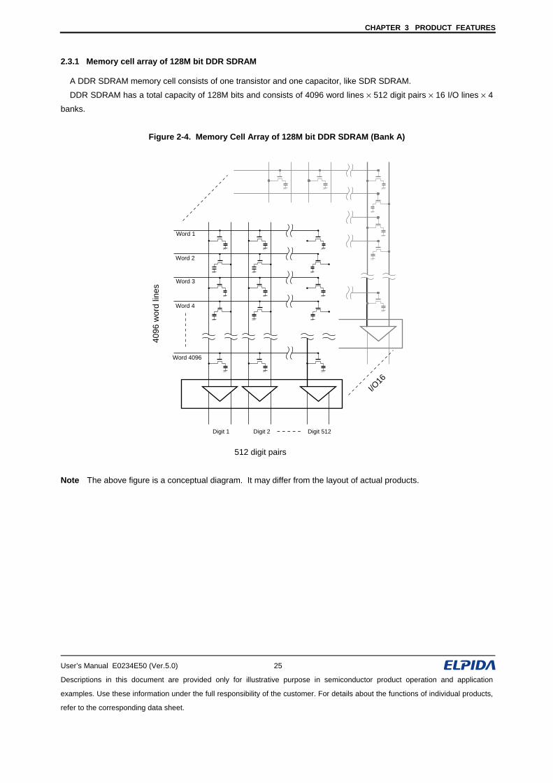
2.3.1 Memory cell array of 128M bit DDR SDRAM
A DDR SDRAM memory cell consists of one transistor and one capacitor, like SDR SDRAM.
DDR SDRAM has a total capacity of 128M bits and consists of 4096 word lines × 512 digit pairs × 16 I/O lines × 4
banks.
Figure 2-4. Memory Cell Array of 128M bit DDR SDRAM (Bank A)
Word 1
Word 2
Word 3
Word 4
Word 4096
Digit 1 Digit 2 Digit 512
I/O16
512 digit pairs
4096
wor
d lin
es
Note The above figure is a conceptual diagram. It may differ from the layout of actual products.
CHAPTER 3 PRODUCT FEATURES
User’s Manual E0234E50 (Ver.5.0) 26
Descriptions in this document are provided only for illustrative purpose in semiconductor product operation and application
examples. Use these information under the full responsibility of the customer. For details about the functions of individual products,
refer to the corresponding data sheet.
2.3.2 Address decoder (Row address decoder, Column address decoder)
Similar to SDR SDRAM, DDR SDRAM employs the address multiplex method. First, a bank address and a row
address are loaded with an active command, and the corresponding word line is selected. Next, a bank address and
a column address are loaded with a read or write command, and the corresponding digit line is selected.
2.3.3 I/O buffer
Buffer for data input/output.
2.3.4 Refresh counter
This counter automatically generates row addresses internally.
2.3.5 DLL (Delay Locked Loop)
DDR SDRAM is provided with a DLL (Delay Locked Loop) circuit. The DLL circuit is designed to realize fast
access and high operation frequencies by controlling and adjusting the time lag between external and internal clock
signals. By employing DLL, timing skew between the clock (CK, /CK) and DQ/DQS is minimized.
CHAPTER 3 PRODUCT FEATURES
User’s Manual E0234E50 (Ver.5.0) 27
Descriptions in this document are provided only for illustrative purpose in semiconductor product operation and application
examples. Use these information under the full responsibility of the customer. For details about the functions of individual products,
refer to the corresponding data sheet.
CHAPTER 3 PRODUCT FEATURES
This chapter explains following features of DDR SDRAM.
(1) Synchronous operation
(2) Command control
(3) Multibank operation
(4) Burst operation
(5) Access time
CHAPTER 3 PRODUCT FEATURES
User’s Manual E0234E50 (Ver.5.0) 28
Descriptions in this document are provided only for illustrative purpose in semiconductor product operation and application
examples. Use these information under the full responsibility of the customer. For details about the functions of individual products,
refer to the corresponding data sheet.
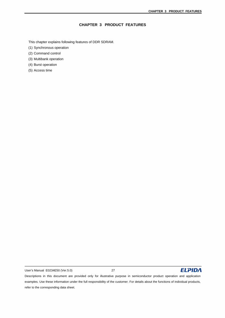
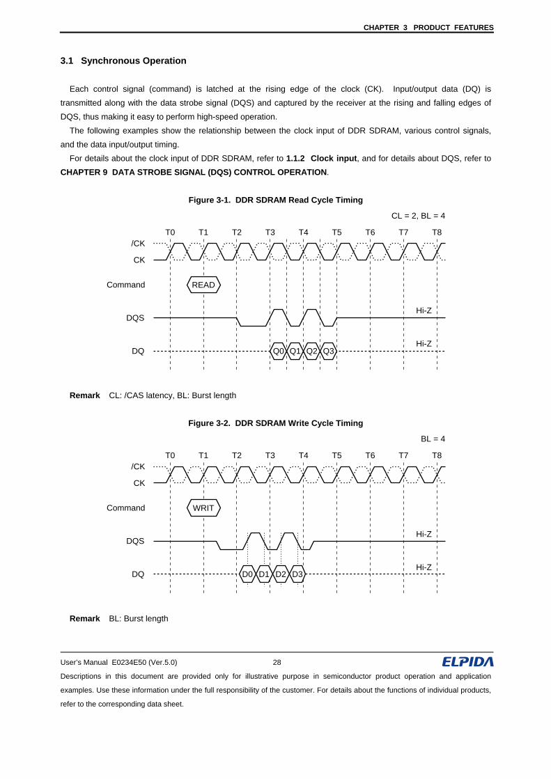
3.1 Synchronous Operation
Each control signal (command) is latched at the rising edge of the clock (CK). Input/output data (DQ) is
transmitted along with the data strobe signal (DQS) and captured by the receiver at the rising and falling edges of
DQS, thus making it easy to perform high-speed operation.
The following examples show the relationship between the clock input of DDR SDRAM, various control signals,
and the data input/output timing. For details about the clock input of DDR SDRAM, refer to 1.1.2 Clock input, and for details about DQS, refer to
CHAPTER 9 DATA STROBE SIGNAL (DQS) CONTROL OPERATION.
Figure 3-1. DDR SDRAM Read Cycle Timing
/CK
Command
DQS
CL = 2, BL = 4
Hi-Z
READ
DQHi-Z
CK
T0 T1 T2 T3 T4 T5 T6 T7 T8
Q0 Q1 Q2 Q3
Remark CL: /CAS latency, BL: Burst length
Figure 3-2. DDR SDRAM Write Cycle Timing
/CK
Command
DQS
BL = 4
Hi-Z
WRIT
DQHi-Z
CK
T0 T1 T2 T3 T4 T5 T6 T7 T8
D0 D1 D2 D3
Remark BL: Burst length
CHAPTER 3 PRODUCT FEATURES
User’s Manual E0234E50 (Ver.5.0) 29
Descriptions in this document are provided only for illustrative purpose in semiconductor product operation and application
examples. Use these information under the full responsibility of the customer. For details about the functions of individual products,
refer to the corresponding data sheet.
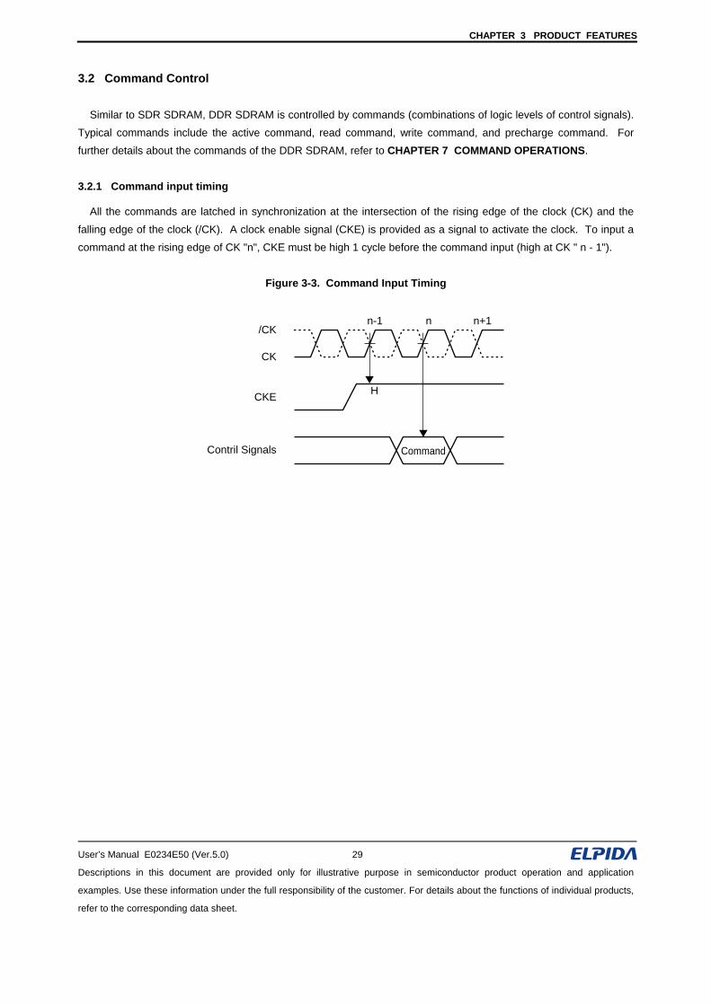
3.2 Command Control
Similar to SDR SDRAM, DDR SDRAM is controlled by commands (combinations of logic levels of control signals).
Typical commands include the active command, read command, write command, and precharge command. For further details about the commands of the DDR SDRAM, refer to CHAPTER 7 COMMAND OPERATIONS.
3.2.1 Command input timing
All the commands are latched in synchronization at the intersection of the rising edge of the clock (CK) and the
falling edge of the clock (/CK). A clock enable signal (CKE) is provided as a signal to activate the clock. To input a
command at the rising edge of CK "n", CKE must be high 1 cycle before the command input (high at CK " n - 1").
Figure 3-3. Command Input Timing
CKE
CK
/CK
H
n-1 n n+1
CommandContril Signals
CHAPTER 3 PRODUCT FEATURES
User’s Manual E0234E50 (Ver.5.0) 30
Descriptions in this document are provided only for illustrative purpose in semiconductor product operation and application
examples. Use these information under the full responsibility of the customer. For details about the functions of individual products,
refer to the corresponding data sheet.
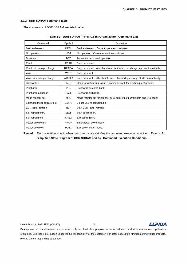
3.2.2 DDR SDRAM command table
The commands of DDR SDRAM are listed below.
Table 3-1. DDR SDRAM (×4/×8/×16-bit Organization) Command List
Command Symbol Operation
Device deselect DESL Device deselect. Current operation continues.
No operation NOP No operation. Current operation continues.
Burst stop BST Terminate burst read operation.
Read READ Start burst read.
Read with auto precharge READA Start burst read. After burst read is finished, precharge starts automatically.
Write WRIT Start burst write.
Write with auto precharge WRITEA Start burst write. After burst write is finished, precharge starts automatically.
Bank active ACT Open (or activate) a row in a particular bank for a subsequent access.
Precharge PRE Precharge selected bank.
Precharge all banks PALL Precharge all banks.
Mode register set MRS Mode register set for latency, burst suquence, burst length and DLL reset.
Extended mode register set EMRS Select DLL enable/disable.
CBR (auto) refresh REF Start CBR (auto) refresh.
Self refresh entry SELF Start self refresh.
Self refresh exit SREX Exit self refresh.
Power down entry PWDN Enter power down mode.
Power down exit PDEX Exit power down mode.
Remark Each operation is valid when the current state satisfies the command execution condition. Refer to 6.1 Simplified State Diagram of DDR SDRAM and 7.2 Command Execution Conditions.
CHAPTER 3 PRODUCT FEATURES
User’s Manual E0234E50 (Ver.5.0) 31
Descriptions in this document are provided only for illustrative purpose in semiconductor product operation and application
examples. Use these information under the full responsibility of the customer. For details about the functions of individual products,
refer to the corresponding data sheet.
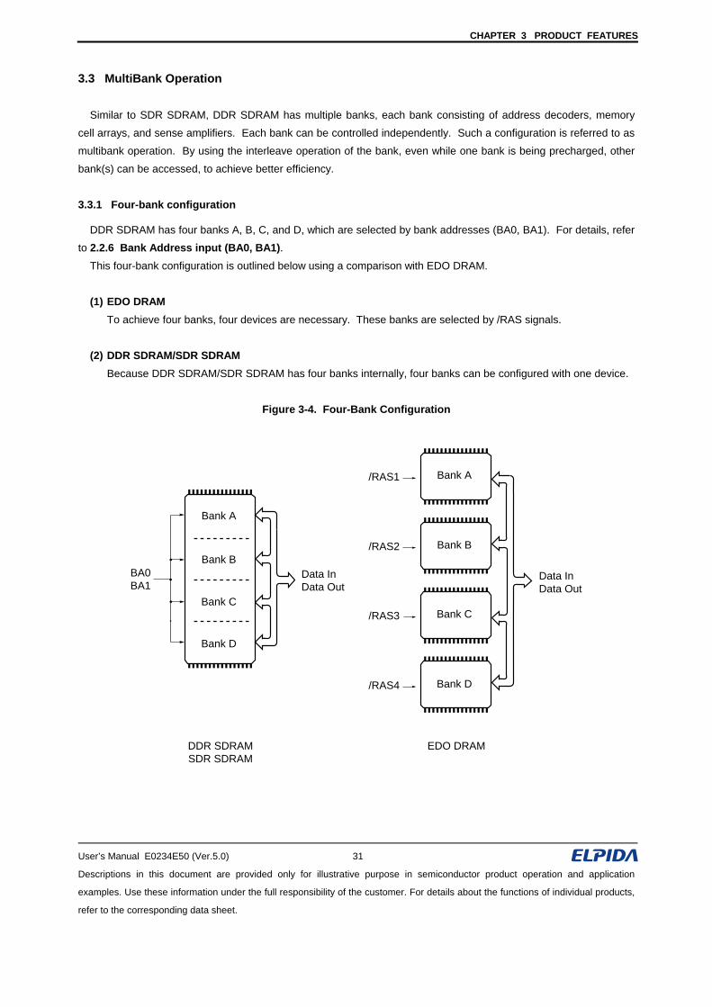
3.3 MultiBank Operation
Similar to SDR SDRAM, DDR SDRAM has multiple banks, each bank consisting of address decoders, memory
cell arrays, and sense amplifiers. Each bank can be controlled independently. Such a configuration is referred to as
multibank operation. By using the interleave operation of the bank, even while one bank is being precharged, other
bank(s) can be accessed, to achieve better efficiency.
3.3.1 Four-bank configuration
DDR SDRAM has four banks A, B, C, and D, which are selected by bank addresses (BA0, BA1). For details, refer to 2.2.6 Bank Address input (BA0, BA1).
This four-bank configuration is outlined below using a comparison with EDO DRAM.
(1) EDO DRAM
To achieve four banks, four devices are necessary. These banks are selected by /RAS signals.
(2) DDR SDRAM/SDR SDRAM
Because DDR SDRAM/SDR SDRAM has four banks internally, four banks can be configured with one device.
Figure 3-4. Four-Bank Configuration
DDR SDRAMSDR SDRAM
BA0BA1
Bank A
Bank D
Bank C
Bank BData InData Out
/RAS3
/RAS4
Bank C
Bank D
/RAS1
/RAS2
Bank A
Bank B
EDO DRAM
Data InData Out
CHAPTER 3 PRODUCT FEATURES
User’s Manual E0234E50 (Ver.5.0) 32
Descriptions in this document are provided only for illustrative purpose in semiconductor product operation and application
examples. Use these information under the full responsibility of the customer. For details about the functions of individual products,
refer to the corresponding data sheet.
3.3.2 Multibank operations
There are various multibank operations depending on the current state and operations that follow.
(1) Burst read/burst write while burst read/burst write for different bank is in progress
Current State (Bank X) Next Operation (Bank Y)
Burst read Completed/Interrupted Burst read
Burst read Completed/Interrupted Burst write
Burst write Completed/Interrupted Burst read
Burst write Completed/Interrupted Burst write
(2) Activate and burst read/burst write while burst read/burst write for different bank is in progress
Current State (Bank X) Next Operation (Bank Y)
Burst read Completed/Interrupted Bank activate and burst read
Burst read Completed/Interrupted Bank activate and burst write
Burst write Completed/Interrupted Bank activate and burst read
Burst write Completed/Interrupted Bank activate and burst write
(3) Burst read/burst write while burst read/burst write with auto precharge for different bank is in progress
Current State (Bank X) Next Operation (Bank Y)
Burst read with auto precharge Completed/Interrupted Burst read
Burst read with auto precharge Completed/Interrupted Burst write
Burst write with auto precharge Completed/Interrupted Burst read
Burst write with auto precharge Completed/Interrupted Burst write
Caution For the detailed timing charts of the operations described above (sections (1), (2), and (3)), refer
to SDR SDRAM User's Manual. All the examples for SDR SDRAM are same as for DDR SDRAM, except /CAS latency and write latency.
CHAPTER 3 PRODUCT FEATURES
User’s Manual E0234E50 (Ver.5.0) 33
Descriptions in this document are provided only for illustrative purpose in semiconductor product operation and application
examples. Use these information under the full responsibility of the customer. For details about the functions of individual products,
refer to the corresponding data sheet.
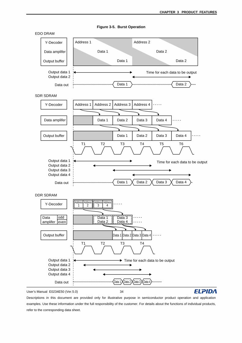
3.4 Burst Operation
Since DDR SDRAM performs pipelined processing internally like SDR SDRAM, it can successively input/output a
fixed number of data in synchronization with an external clock.
In pipelined architecture, operations from column address input to data input/output are divided into several
processing blocks, each block operating in parallel to boost the transfer capability.
Burst transfer in EDO DRAM, SDR SDRAM, and DDR SDRAM is explained below using the read cycle as an
example.
(1) EDO DRAM
The next read operation has to wait until a series of operations, from address input to data output, is completed.
(2) SDR SDRAM
A column operation is divided into three processing blocks (Y-decoder, Data amplifier and Output buffer). As
each processing block can operate in parallel, each block can start the next process as soon as the current
process is finished and handed over to the next processing block. When a column address is input, the
internal address counter automatically increments the internal column address in synchronization with the clock
(CK). The number of times the column address is incremented is determined by the burst length.
This internal structure enables reading or writing of successive address. Data is continuously output in
synchronization with the rising edge of CK.
(3) DDR SDRAM
The basic transfer scheme is the same as SDR SDRAM, except that a 2-bit prefetch architecture is employed
by DDR SDRAM.
In this architecture, 2n bits of data are transferred from the memory cell array to the I/O buffer every clock
cycle. Data transferred to the I/O buffer is output n bits at a time (even and odd addresses) every half-clock
cycle. As a result, data is output continuously in synchronization with the rising and falling edges of the clock. For further details about 2-bit prefetch architecture, refer to 1.1.1 Data transfer frequency, data rate.
(4) Comparison between EDO DRAM, SDR SDRAM and DDR SDRAM
The time required for first data output is almost the same for all these DRAMs. But when it's a successive data
access, SDR SDRAM and DDR SDRAM can achieve a faster data transfer rate than EDO DRAM due to the
pipelined operation. DDR SDRAM, which uses 2-bit prefetch architecture, achieves an even faster data
transfer rate than SDR SDRAM.
CHAPTER 3 PRODUCT FEATURES
User’s Manual E0234E50 (Ver.5.0) 34
Descriptions in this document are provided only for illustrative purpose in semiconductor product operation and application
examples. Use these information under the full responsibility of the customer. For details about the functions of individual products,
refer to the corresponding data sheet.
Figure 3-5. Burst Operation
Y-Decoder
Data 2 Data 3 Data 4Data 1
Data amplifer
Output buffer
oddeven
Output data 1Output data 2Output data 3Output data 4
Data out Data 2 Data 3 Data 4Data 1
Address2
Data 1Data 2
Data 3Data 4
DDR SDRAM
Address1
Address4
Address3
Time for each data to be output
Y-Decoder Address 1 Address 2 Address 3 Address 4
Data 1 Data 2 Data 3 Data 4
Data 1 Data 2 Data 3 Data 4
Data amplifer
Output buffer
T1 T2 T3 T4
T1 T2 T3 T4
T5 T6
Output data 1Output data 2Output data 3Output data 4
Data out Data 2 Data 3 Data 4Data 1
SDR SDRAM
Time for each data to be output
Time for each data to be output
Address 1 Address 2
Data 1 Data 2
Data 1 Data 2
Y-Decoder
Data amplifer
Output buffer
Output data 1Output data 2
Data out Data 2Data 1
EDO DRAM
CHAPTER 3 PRODUCT FEATURES
User’s Manual E0234E50 (Ver.5.0) 35
Descriptions in this document are provided only for illustrative purpose in semiconductor product operation and application
examples. Use these information under the full responsibility of the customer. For details about the functions of individual products,
refer to the corresponding data sheet.
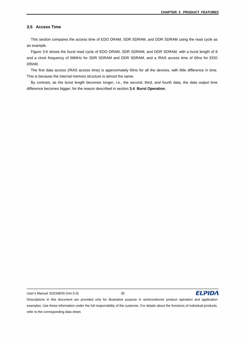
3.5 Access Time
This section compares the access time of EDO DRAM, SDR SDRAM, and DDR SDRAM using the read cycle as
an example.
Figure 3-6 shows the burst read cycle of EDO DRAM, SDR SDRAM, and DDR SDRAM, with a burst length of 8
and a clock frequency of 66MHz for SDR SDRAM and DDR SDRAM, and a /RAS access time of 60ns for EDO
DRAM.
The first data access (/RAS access time) is approximately 60ns for all the devices, with little difference in time.
This is because the internal memory structure is almost the same.
By contrast, as the burst length becomes longer, i.e., the second, third, and fourth data, the data output time difference becomes bigger, for the reason described in section 3.4 Burst Operation.
CHAPTER 3 PRODUCT FEATURES
User’s Manual E0234E50 (Ver.5.0) 36
Descriptions in this document are provided only for illustrative purpose in semiconductor product operation and application
examples. Use these information under the full responsibility of the customer. For details about the functions of individual products,
refer to the corresponding data sheet.
Figure 3-6. Burst Read Cycle
BL = 8
/CK
Command
DQS Hi-Z
ACT READ
Address Row Column
Data out Hi-Z
CK
T0 T1 T2 T3 T4 T5 T6 T7 T8 T9 T10 T11 T12 T13
Q0 Q1 Q2 Q3 Q4 Q5 Q6 Q7
15 ns
60 ns
Address Row Column
CK
Command ACT READ
Data out Hi-Z
T0 T1 T2 T3 T4 T5 T6 T7 T8 T9 T10 T11 T12 T13
Q0 Q1 Q2 Q3 Q4 Q5 Q6 Q7
15 ns
60 ns
60 ns
/WE
/RAS
/CAS
Data out Q1 Q2 Q3 Q4 Q5
25 ns
EDO DRAM
SDR SDRAM
DDR SDRAM
Q0
High level
Caution EDO DRAM is asynchronous. Remark BL: Burst length
CHAPTER 3 PRODUCT FEATURES
User’s Manual E0234E50 (Ver.5.0) 37
Descriptions in this document are provided only for illustrative purpose in semiconductor product operation and application
examples. Use these information under the full responsibility of the customer. For details about the functions of individual products,
refer to the corresponding data sheet.
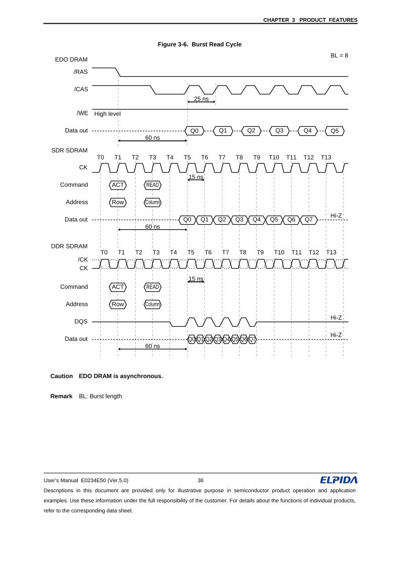
Figure 3-7. Access Time of DDR SDRAM, SDR SDRAM and EDO DRAM
Access time (ns)
Bur
st c
ycle
tim
e
7
6
2
3
4
5
1
5030 70 90 110 130 150
8
EDO DRAM
SDR SDRAMDDR SDRAM
DDR SDRAM
66MHz
133MHz
133MHz
SDR SDRAM66MHz
Table 3-2. Access Time of DDR SDRAM, SDR SDRAM and EDO DRAM
Access time EDO DRAM SDR SDRAM DDR SDRAM EDO DRAM SDR SDRAM DDR SDRAM SDR SDRAM DDR SDRAM
–60 66 MHz 66 MHz –50 100 MHz 100 MHz 133 MHz 133 MHz
(15 ns) (15 ns) (10 ns) (10 ns) (7.5 ns) (7.5 ns)
1st access 60 ns 50 ns 45 ns
2nd access 85 ns 75 ns 67.5 ns 70 ns 60 ns 55 ns 52.5 ns 48.75 ns
3rd access 110 ns 90 ns 75 ns 90 ns 70 ns 60 ns 60 ns 52.5 ns
4th access 135 ns 105 ns 82.5 ns 110 ns 80 ns 65 ns 67.5 ns 56.25 ns
5th access 160 ns 120 ns 90 ns 130 ns 90 ns 70 ns 75 ns 60 ns
6th access 185 ns 135 ns 97.5 ns 150 ns 100 ns 75 ns 82.5 ns 63.75 ns
7th access 210 ns 150 ns 105 ns 170 ns 110 ns 80 ns 90 ns 67.5 ns
8th access 235 ns 165 ns 112.5 ns 190 ns 120 ns 85 ns 97.5 ns 71.25 ns
CHAPTER 4 INITIALIZATION
User’s Manual E0234E50 (Ver.5.0) 38
Descriptions in this document are provided only for illustrative purpose in semiconductor product operation and application
examples. Use these information under the full responsibility of the customer. For details about the functions of individual products,
refer to the corresponding data sheet.
CHAPTER 4 INITIALIZATION
This chapter explains initialization after power on.
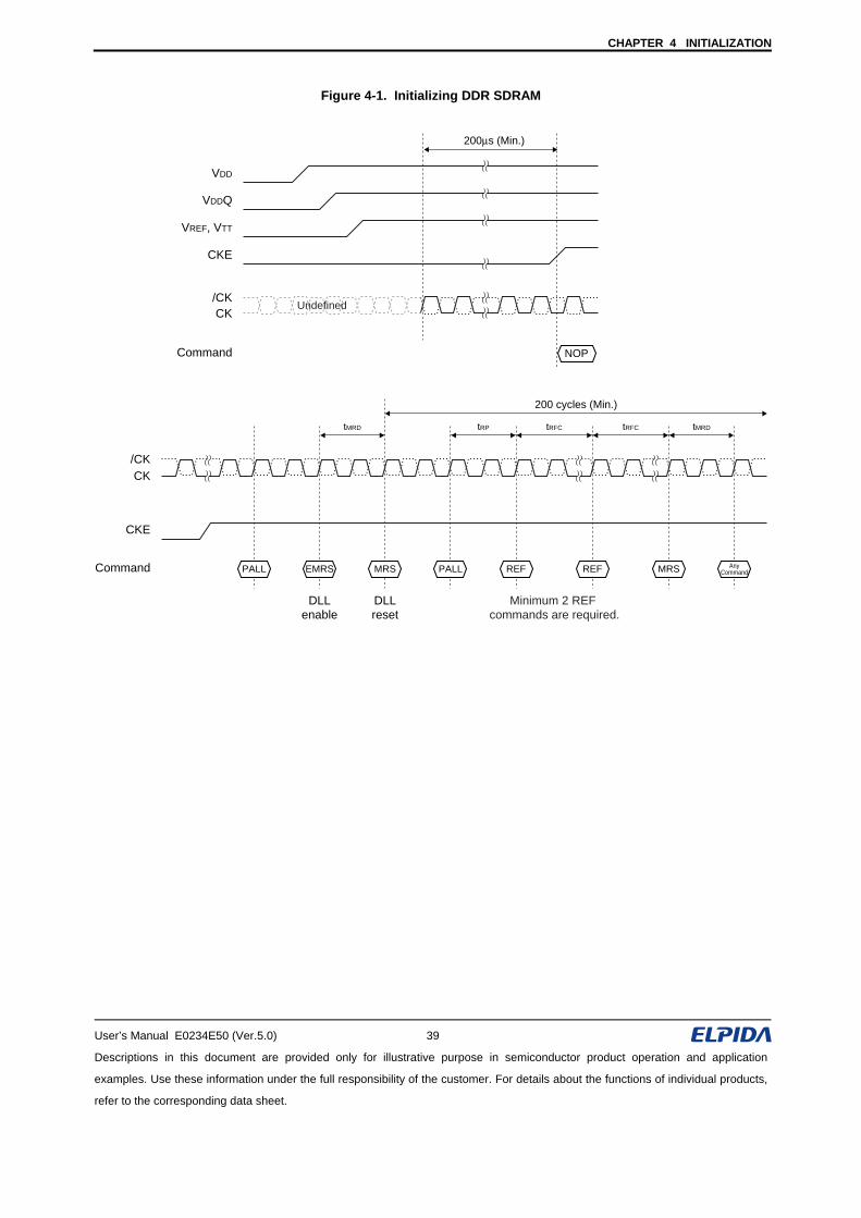
4.1 Initialization after Power On
The logical state of the internal circuit of DDR SDRAM is undefined right after power on. DDR SDRAMs must be
powered up and initialized in a predefined manner to ensure correct operation. DDR SDRAM power-on and
initialization sequence is as follows.
(1) Apply power first to VDD, then to VDDQ, and finally to VREF and VTT.
(2) Keep the clock enable signal (CKE) low in order to guarantee that DQ and DQS pins will be in the high
impedance state.
(3) After all power supply and reference voltages are stable, and the clock is stable, wait 200μs before applying an
executable command. Once the 200μs delay has been satisfied, a device deselect command (DESL) or no
operation command (NOP) must be applied and CKE must be made high.
(4) Precharge all banks (the precharge all banks command (PALL) is recommended).
(5) Enable DLL by the extended mode register set command (EMRS). Then reset DLL by the mode register set
command (MRS) with A8 high. 200 cycles are required between DLL reset and any read command.
(6) After precharging all the banks again, input two or more CBR (auto) refresh commands (REF).
(7) Input the mode register set command (MRS) to program the operating parameters.
After initialization is finished, do not change clock frequency except during self refresh mode.
CHAPTER 4 INITIALIZATION
User’s Manual E0234E50 (Ver.5.0) 39
Descriptions in this document are provided only for illustrative purpose in semiconductor product operation and application
examples. Use these information under the full responsibility of the customer. For details about the functions of individual products,
refer to the corresponding data sheet.
Figure 4-1. Initializing DDR SDRAM
CK
Command
Command
tRP tMRDtRFC tRFCtMRD
CKE
200 cycles (Min.)
PALL EMRS MRS PALL REF REF MRS AnyCommand
DLLenable
DLLreset
Minimum 2 REF commands are required.
VDD
VDDQ
VREF, VTT
CKE
/CK
CK/CK
NOP
200μs (Min.)
Undefined
CHAPTER 5 MODE REGISTER SET
User’s Manual E0234E50 (Ver.5.0) 40
Descriptions in this document are provided only for illustrative purpose in semiconductor product operation and application
examples. Use these information under the full responsibility of the customer. For details about the functions of individual products,
refer to the corresponding data sheet.
CHAPTER 5 MODE REGISTER SET
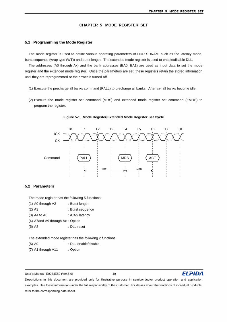
5.1 Programming the Mode Register
The mode register is used to define various operating parameters of DDR SDRAM, such as the latency mode,
burst sequence (wrap type (WT)) and burst length. The extended mode register is used to enable/disable DLL.
The addresses (A0 through Ax) and the bank addresses (BA0, BA1) are used as input data to set the mode
register and the extended mode register. Once the parameters are set, these registers retain the stored information
until they are reprogrammed or the power is turned off.
(1) Execute the precharge all banks command (PALL) to precharge all banks. After tRP, all banks become idle.
(2) Execute the mode register set command (MRS) and extended mode register set command (EMRS) to
program the register.
Figure 5-1. Mode Register/Extended Mode Register Set Cycle
/CK
Command PALL MRS ACT
CK
T0 T1 T2 T3 T4 T5 T6 T7 T8
tRP tMRD
5.2 Parameters
The mode register has the following 5 functions:
(1) A0 through A2 : Burst length
(2) A3 : Burst sequence
(3) A4 to A6 : /CAS latency
(4) A7and A9 through Ax : Option
(5) A8 : DLL reset
The extended mode register has the following 2 functions:
(6) A0 : DLL enable/disable
(7) A1 through A11 : Option
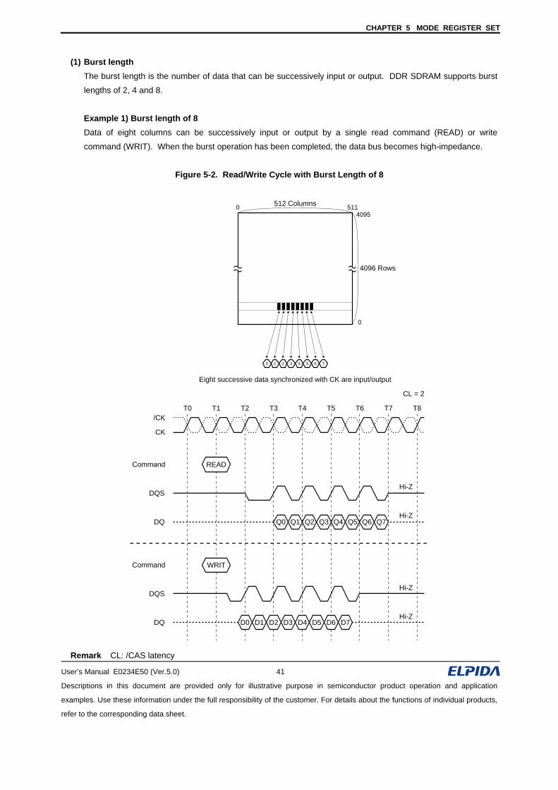
CHAPTER 5 MODE REGISTER SET
User’s Manual E0234E50 (Ver.5.0) 41
Descriptions in this document are provided only for illustrative purpose in semiconductor product operation and application
examples. Use these information under the full responsibility of the customer. For details about the functions of individual products,
refer to the corresponding data sheet.
(1) Burst length The burst length is the number of data that can be successively input or output. DDR SDRAM supports burst
lengths of 2, 4 and 8.
Example 1) Burst length of 8 Data of eight columns can be successively input or output by a single read command (READ) or write
command (WRIT). When the burst operation has been completed, the data bus becomes high-impedance.
Figure 5-2. Read/Write Cycle with Burst Length of 8
512 Columns
4096 Rows
0 5114095
0
Eight successive data synchronized with CK are input/output
Command
DQSHi-Z
DQHi-Z
0 1 2 3 4 5 6 7
D0 D1 D2 D3 D4 D5 D6 D7
/CK
Command
DQSHi-Z
READ
DQHi-Z
CK
T0 T1 T2 T3 T4 T5 T6 T7 T8
Q0 Q1 Q2 Q3 Q4 Q5 Q6 Q7
WRIT
CL = 2
Remark CL: /CAS latency
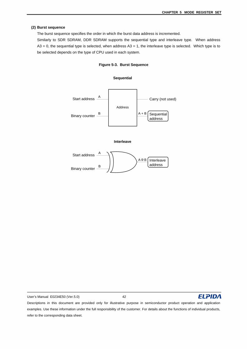
CHAPTER 5 MODE REGISTER SET
User’s Manual E0234E50 (Ver.5.0) 42
Descriptions in this document are provided only for illustrative purpose in semiconductor product operation and application
examples. Use these information under the full responsibility of the customer. For details about the functions of individual products,
refer to the corresponding data sheet.
(2) Burst sequence The burst sequence specifies the order in which the burst data address is incremented.
Similarly to SDR SDRAM, DDR SDRAM supports the sequential type and interleave type. When address
A3 = 0, the sequential type is selected, when address A3 = 1, the interleave type is selected. Which type is to
be selected depends on the type of CPU used in each system.
Figure 5-3. Burst Sequence
A
B
Start address
Binary counter
A
B
Start address
Binary counter
Carry (not used)
A + B Sequentialaddress
Address
Sequential
Interleave
Interleaveaddress
A + B
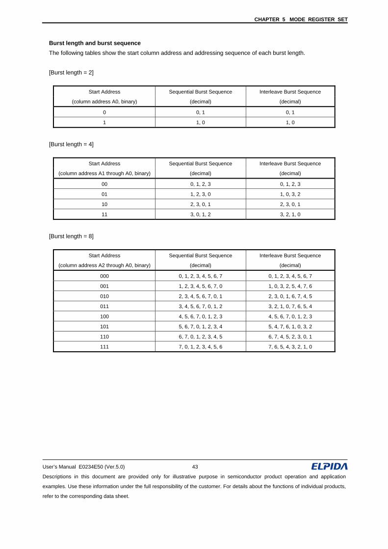
CHAPTER 5 MODE REGISTER SET
User’s Manual E0234E50 (Ver.5.0) 43
Descriptions in this document are provided only for illustrative purpose in semiconductor product operation and application
examples. Use these information under the full responsibility of the customer. For details about the functions of individual products,
refer to the corresponding data sheet.
Burst length and burst sequence The following tables show the start column address and addressing sequence of each burst length.
[Burst length = 2]
Start Address Sequential Burst Sequence Interleave Burst Sequence
(column address A0, binary) (decimal) (decimal)
0 0, 1 0, 1
1 1, 0 1, 0
[Burst length = 4]
Start Address Sequential Burst Sequence Interleave Burst Sequence
(column address A1 through A0, binary) (decimal) (decimal)
00 0, 1, 2, 3 0, 1, 2, 3
01 1, 2, 3, 0 1, 0, 3, 2
10 2, 3, 0, 1 2, 3, 0, 1
11 3, 0, 1, 2 3, 2, 1, 0
[Burst length = 8]
Start Address Sequential Burst Sequence Interleave Burst Sequence
(column address A2 through A0, binary) (decimal) (decimal)
000 0, 1, 2, 3, 4, 5, 6, 7 0, 1, 2, 3, 4, 5, 6, 7
001 1, 2, 3, 4, 5, 6, 7, 0 1, 0, 3, 2, 5, 4, 7, 6
010 2, 3, 4, 5, 6, 7, 0, 1 2, 3, 0, 1, 6, 7, 4, 5
011 3, 4, 5, 6, 7, 0, 1, 2 3, 2, 1, 0, 7, 6, 5, 4
100 4, 5, 6, 7, 0, 1, 2, 3 4, 5, 6, 7, 0, 1, 2, 3
101 5, 6, 7, 0, 1, 2, 3, 4 5, 4, 7, 6, 1, 0, 3, 2
110 6, 7, 0, 1, 2, 3, 4, 5 6, 7, 4, 5, 2, 3, 0, 1
111 7, 0, 1, 2, 3, 4, 5, 6 7, 6, 5, 4, 3, 2, 1, 0
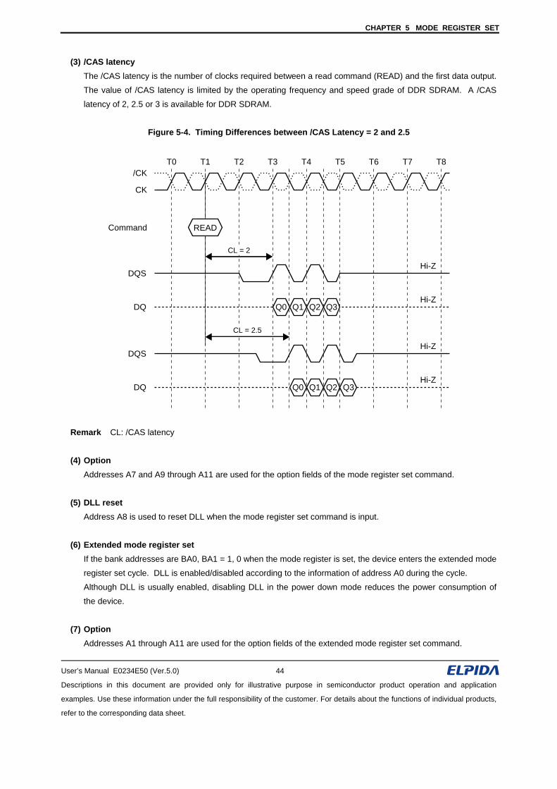
CHAPTER 5 MODE REGISTER SET
User’s Manual E0234E50 (Ver.5.0) 44
Descriptions in this document are provided only for illustrative purpose in semiconductor product operation and application
examples. Use these information under the full responsibility of the customer. For details about the functions of individual products,
refer to the corresponding data sheet.
(3) /CAS latency The /CAS latency is the number of clocks required between a read command (READ) and the first data output.
The value of /CAS latency is limited by the operating frequency and speed grade of DDR SDRAM. A /CAS
latency of 2, 2.5 or 3 is available for DDR SDRAM.
Figure 5-4. Timing Differences between /CAS Latency = 2 and 2.5
/CK
Command
DQS
DQ
CK
T0 T1 T2 T3 T4 T5 T6 T7 T8
Q0 Q1 Q2 Q3
DQS
DQ Q0 Q1 Q2 Q3
READ
Hi-Z
Hi-Z
Hi-Z
Hi-Z
CL = 2
CL = 2.5
Remark CL: /CAS latency
(4) Option
Addresses A7 and A9 through A11 are used for the option fields of the mode register set command.
(5) DLL reset
Address A8 is used to reset DLL when the mode register set command is input.
(6) Extended mode register set
If the bank addresses are BA0, BA1 = 1, 0 when the mode register is set, the device enters the extended mode
register set cycle. DLL is enabled/disabled according to the information of address A0 during the cycle.
Although DLL is usually enabled, disabling DLL in the power down mode reduces the power consumption of
the device.
(7) Option
Addresses A1 through A11 are used for the option fields of the extended mode register set command.
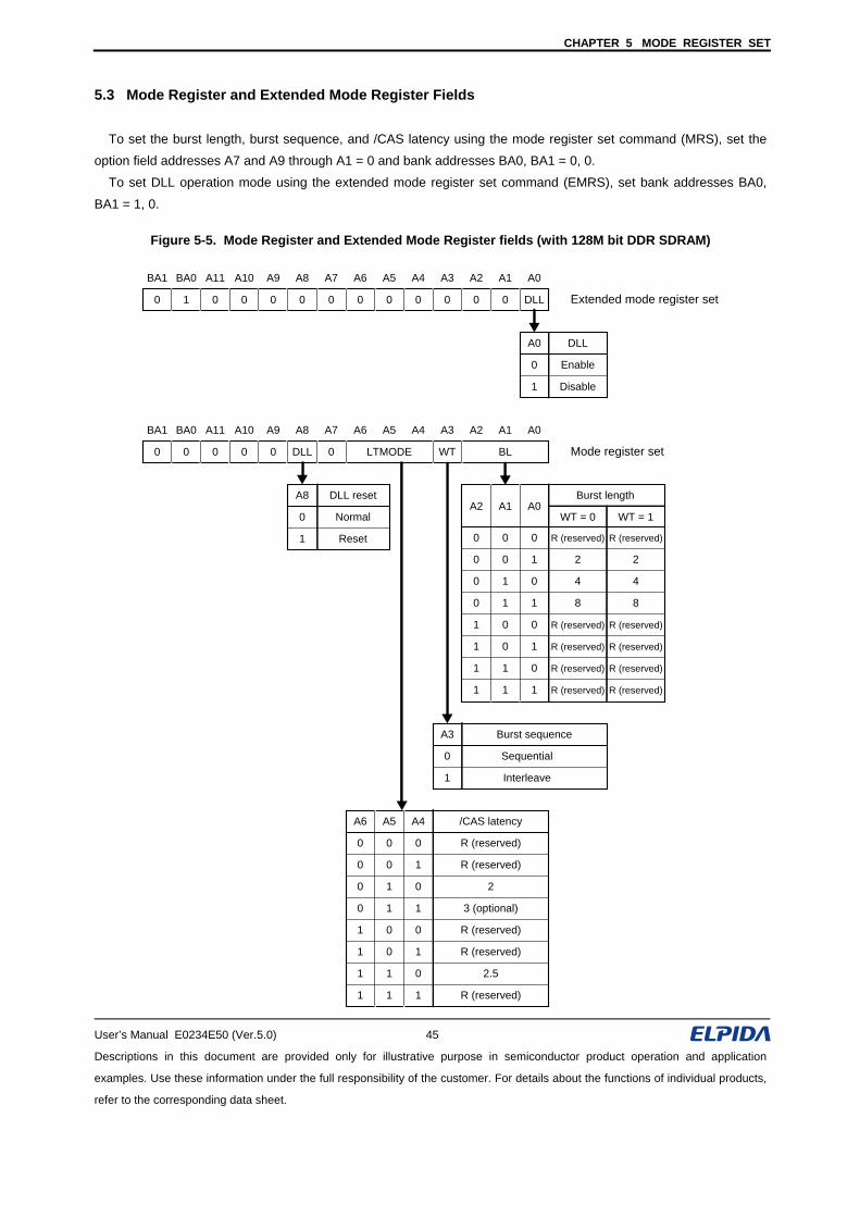
CHAPTER 5 MODE REGISTER SET
User’s Manual E0234E50 (Ver.5.0) 45
Descriptions in this document are provided only for illustrative purpose in semiconductor product operation and application
examples. Use these information under the full responsibility of the customer. For details about the functions of individual products,
refer to the corresponding data sheet.
5.3 Mode Register and Extended Mode Register Fields
To set the burst length, burst sequence, and /CAS latency using the mode register set command (MRS), set the
option field addresses A7 and A9 through A1 = 0 and bank addresses BA0, BA1 = 0, 0.
To set DLL operation mode using the extended mode register set command (EMRS), set bank addresses BA0,
BA1 = 1, 0.
Figure 5-5. Mode Register and Extended Mode Register fields (with 128M bit DDR SDRAM)
BA1 BA0 A11 A10 A9 A8 A7 A6 A5 A4 A3 A2 A1 A0
0 1 0 0 0 0 0 0 0 0 0 0 0
0 0 0
0 0 1
0 1 0
0 1 1
1 0 0
1 0 1
1 1 0
1 1 1
DLL Extended mode register set
0
1
A0 DLL
Enable
Disable
BA1 BA0 A11 A10 A9 A8 A7 A6 A5 A4 A3 A2 A1 A0
0 0 0 0 0 DLL 0 LTMODE WT BL Mode register set
A8 DLL reset
Burst sequence
0
1
Normal
Reset
A3
0
1
Sequential
Interleave
A2 A1 A0WT = 0 WT = 1
R (reserved) R (reserved)
R (reserved) R (reserved)
R (reserved) R (reserved)
R (reserved) R (reserved)
R (reserved) R (reserved)
2 2
4 4
8 8
0 0 0
0 0 1
0 1 0
0 1 1
1 0 0
1 0 1
1 1 0
1 1 1
A6 A5 A4 /CAS latency
R (reserved)
R (reserved)
3 (optional)
R (reserved)
R (reserved)
R (reserved)
2
2.5
Burst length
CHAPTER 6 SIMPLIFIED STATE DIAGRAM
User’s Manual E0234E50 (Ver.5.0) 46
Descriptions in this document are provided only for illustrative purpose in semiconductor product operation and application
examples. Use these information under the full responsibility of the customer. For details about the functions of individual products,
refer to the corresponding data sheet.
CHAPTER 6 SIMPLIFIED STATE DIAGRAM
6.1 Simplified State Diagram of DDR SDRAM
Figure 6-1 shows a simplified state diagram of DDR SDRAM. Circles in the figure indicate the current state, and
arrows indicate the allowable transition.
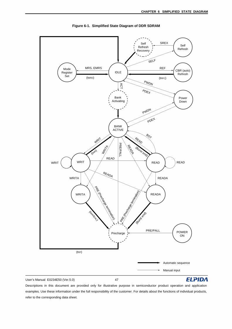
CHAPTER 6 SIMPLIFIED STATE DIAGRAM
User’s Manual E0234E50 (Ver.5.0) 47
Descriptions in this document are provided only for illustrative purpose in semiconductor product operation and application
examples. Use these information under the full responsibility of the customer. For details about the functions of individual products,
refer to the corresponding data sheet.
Figure 6-1. Simplified State Diagram of DDR SDRAM
WR
ITA
PRE/PALL
PR
E/P
ALL
RE
AD
A
READWRIT
BSTP
RE
(Precharge term
ination)PR
E (P
rech
arge
term
inat
ion)
AC
T
MRS, EMRS REF
PWDN
PDEX
SELF
IDLEMode
RegisterSet
CBR (auto)Refresh
BANKACTIVE
SelfRefresh
PowerDown
Precharge
READ
READA
POWERON
WRIT READ
Automatic sequence
Manual input
READ
SelfRefresh
Recovery
Bank Activating
SREX
READAREADAWRITA
(tRP)
(Bur
st e
nd)
(tWR/tDAL)
(tWR)
(Burst end)
(tMRD) (tRFC)
WRITA
WRIT
PWDN
PDEX
CHAPTER 6 SIMPLIFIED STATE DIAGRAM
User’s Manual E0234E50 (Ver.5.0) 48
Descriptions in this document are provided only for illustrative purpose in semiconductor product operation and application
examples. Use these information under the full responsibility of the customer. For details about the functions of individual products,
refer to the corresponding data sheet.
6.2 Current State Definition
6.2.1 Idle (IDLE)
The state in which the bank has been precharged and tRP has been satisfied. The bank active command (ACT),
mode register set command (MRS, EMRS) and refresh command (REF, SELF) may only be issued when the device
or the bank to be selected is in the idle state.
6.2.2 Bank activating (Row activating)
For an operation (read or write) for a particular row in a particular bank, the bank has to be activated first to
receive an operation request (read or write command).
Bank activating is the state in which the bank active command (ACT) has been issued but tRCD has not been
satisfied. The device automatically changes states from bank activating to bank active when tRCD is satisfied.
6.2.3 Bank active (BANK ACTIVE) (Row active)
When tRCD is satisfied (bank active), the device is ready to receive an operation request (read or write command).
6.2.4 Precharging
When current operation (read or write) is finished, the bank has to be idle state at first to activate a different row in
the bank. To return to the idle state, the precharge command (PRE, PALL) has to be issued.
Precharging is the state in which the precharge command has been issued but tRP has not been satisfied. As mentioned in 6.2.1 Idle (IDLE), the bank will return to idle state when tRP is satisfied.
6.2.5 Read and write (READ, WRIT)
The state in which a read or write operation is in progress. By issuing the read or write command (READ, WRIT)
along with a column address for the active bank, the read or write operation will start.
When the operation is completed, the bank automatically returns to the bank active state.
6.2.6 Read and write with auto precharge (READA, WRITA)
When the read or write with auto precharge command (READA, WRITA) is issued, the device automatically starts
precharging and the bank returns to the idle state after the read or write operation is completed.
6.2.7 Mode register set
The mode register set or extended mode register set command (MRS, EMRS) can only be issued when all banks
of the device are in the idle state. When data has been written to the mode register, the device automatically returns
to the idle state after tMRD.
6.2.8 CBR (Auto) refresh
The CBR (auto) refresh command (REF) can only be issued when all banks of the device are in the idle state.
When the REF command is issued, a certain row address of every bank is selected, and refresh is executed. When
CBR (auto) refresh is completed, the device automatically returns to the idle state after tRFC.
CHAPTER 6 SIMPLIFIED STATE DIAGRAM
User’s Manual E0234E50 (Ver.5.0) 49
Descriptions in this document are provided only for illustrative purpose in semiconductor product operation and application
examples. Use these information under the full responsibility of the customer. For details about the functions of individual products,
refer to the corresponding data sheet.
6.2.9 Self refresh
The self refresh command (SELF) can only be issued when all banks of the device are in the idle state. In the self
refresh state, the device automatically performs refresh. It is not necessary to execute the refresh command
externally.
6.2.10 Self refresh recovery
The state in which the self refresh exit command (SREX) has been issued but tXSNR has not been satisfied. The
device automatically returns to the idle state after tXSNR.
6.2.11 Power down
When the clock enable signal (CKE) is made low in the idle state or bank active state, power down mode is set. In
this mode, all input buffers except clock (CK, /CK) and CKE are turned off to reduce the power consumption of the
device.
To return to the original state (idle or active), CKE must return to high.
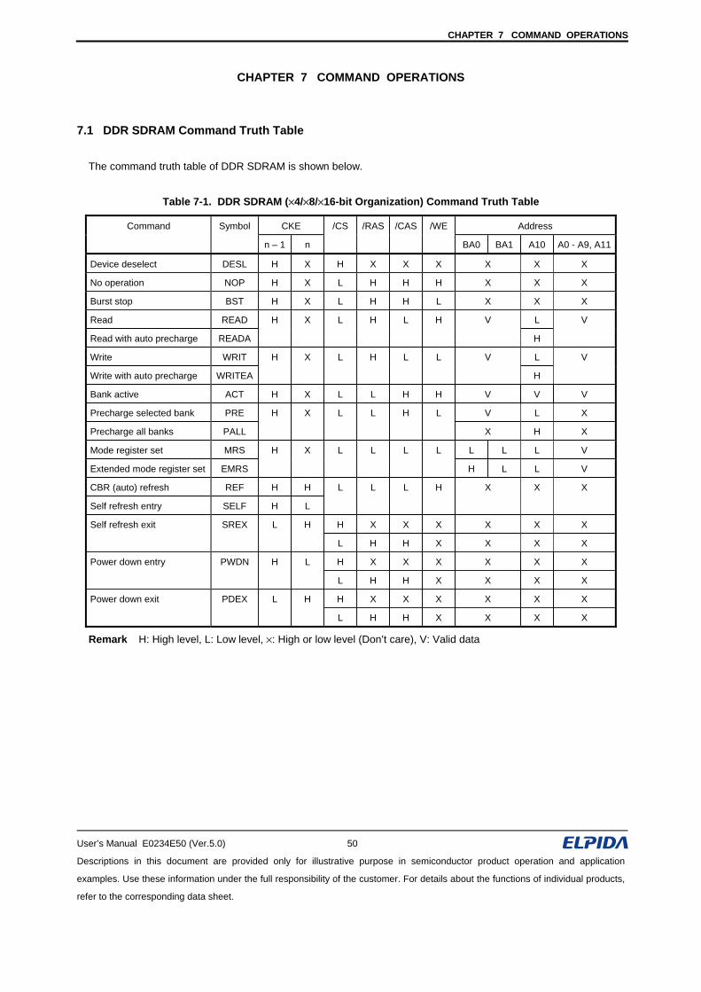
CHAPTER 7 COMMAND OPERATIONS
User’s Manual E0234E50 (Ver.5.0) 50
Descriptions in this document are provided only for illustrative purpose in semiconductor product operation and application
examples. Use these information under the full responsibility of the customer. For details about the functions of individual products,
refer to the corresponding data sheet.
CHAPTER 7 COMMAND OPERATIONS
7.1 DDR SDRAM Command Truth Table
The command truth table of DDR SDRAM is shown below.
Table 7-1. DDR SDRAM (×4/×8/×16-bit Organization) Command Truth Table
Command Symbol CKE /CS /RAS /CAS /WE Address
n – 1 n BA0 BA1 A10 A0 - A9, A11
Device deselect DESL H X H X X X X X X
No operation NOP H X L H H H X X X
Burst stop BST H X L H H L X X X
Read READ H X L H L H V L V
Read with auto precharge READA H
Write WRIT H X L H L L V L V
Write with auto precharge WRITEA H
Bank active ACT H X L L H H V V V
Precharge selected bank PRE H X L L H L V L X
Precharge all banks PALL X H X
Mode register set MRS H X L L L L L L L V
Extended mode register set EMRS H L L V
CBR (auto) refresh REF H H L L L H X X X
Self refresh entry SELF H L
Self refresh exit SREX L H H X X X X X X
L H H X X X X
Power down entry PWDN H L H X X X X X X
L H H X X X X
Power down exit PDEX L H H X X X X X X
L H H X X X X
Remark H: High level, L: Low level, ×: High or low level (Don’t care), V: Valid data
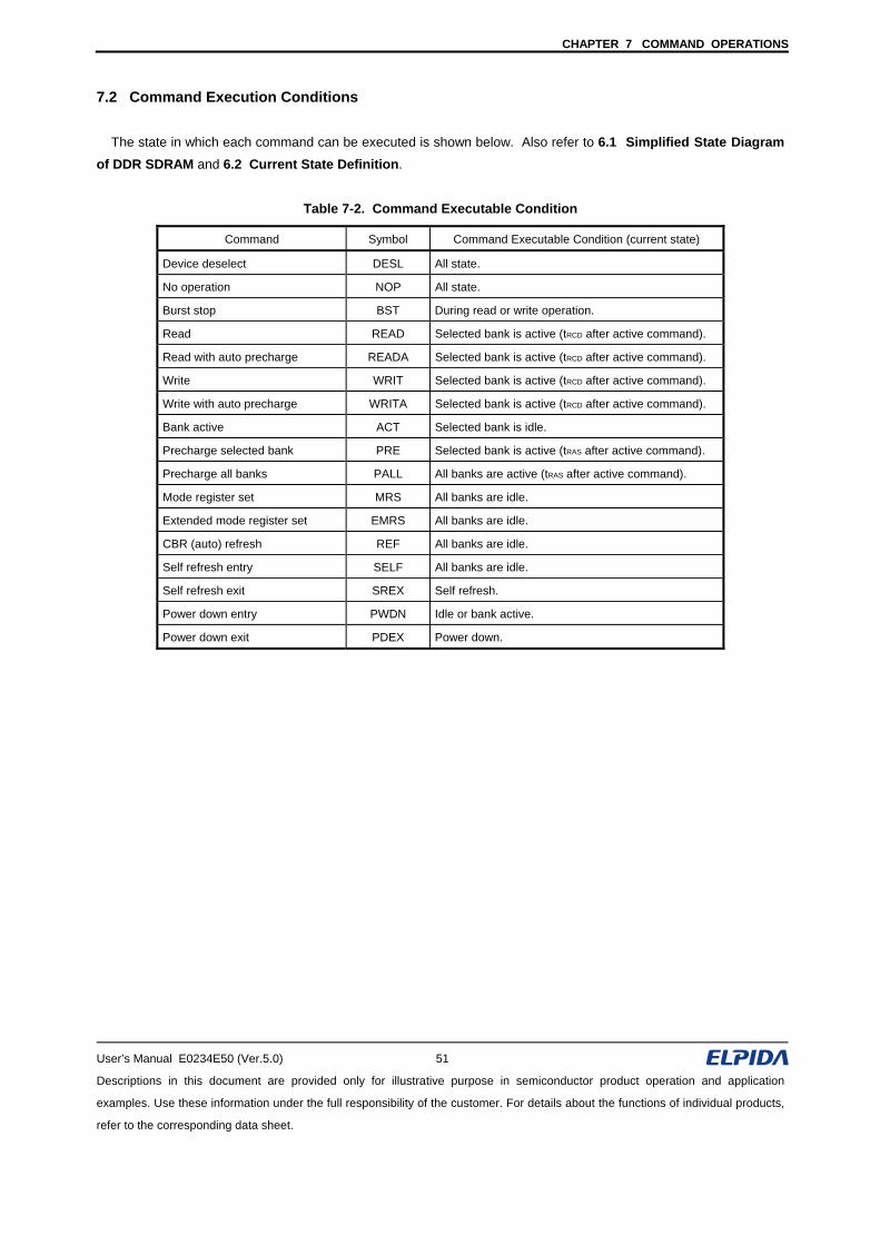
CHAPTER 7 COMMAND OPERATIONS
User’s Manual E0234E50 (Ver.5.0) 51
Descriptions in this document are provided only for illustrative purpose in semiconductor product operation and application
examples. Use these information under the full responsibility of the customer. For details about the functions of individual products,
refer to the corresponding data sheet.
7.2 Command Execution Conditions The state in which each command can be executed is shown below. Also refer to 6.1 Simplified State Diagram
of DDR SDRAM and 6.2 Current State Definition.
Table 7-2. Command Executable Condition
Command Symbol Command Executable Condition (current state)
Device deselect DESL All state.
No operation NOP All state.
Burst stop BST During read or write operation.
Read READ Selected bank is active (tRCD after active command).
Read with auto precharge READA Selected bank is active (tRCD after active command).
Write WRIT Selected bank is active (tRCD after active command).
Write with auto precharge WRITA Selected bank is active (tRCD after active command).
Bank active ACT Selected bank is idle.
Precharge selected bank PRE Selected bank is active (tRAS after active command).
Precharge all banks PALL All banks are active (tRAS after active command).
Mode register set MRS All banks are idle.
Extended mode register set EMRS All banks are idle.
CBR (auto) refresh REF All banks are idle.
Self refresh entry SELF All banks are idle.
Self refresh exit SREX Self refresh.
Power down entry PWDN Idle or bank active.
Power down exit PDEX Power down.
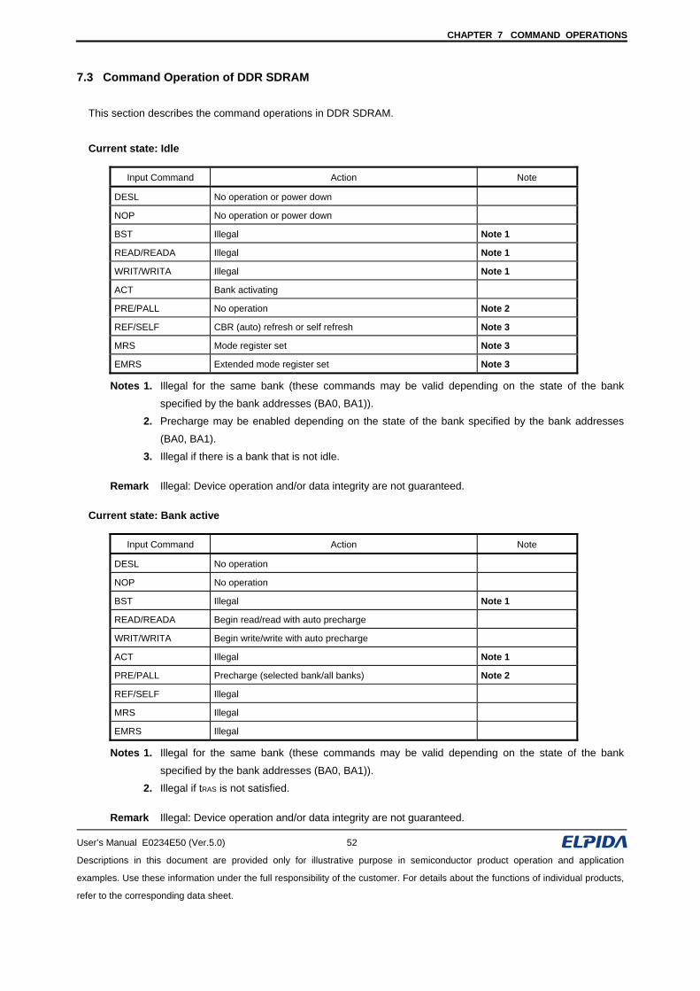
CHAPTER 7 COMMAND OPERATIONS
User’s Manual E0234E50 (Ver.5.0) 52
Descriptions in this document are provided only for illustrative purpose in semiconductor product operation and application
examples. Use these information under the full responsibility of the customer. For details about the functions of individual products,
refer to the corresponding data sheet.
7.3 Command Operation of DDR SDRAM
This section describes the command operations in DDR SDRAM.
Current state: Idle
Input Command Action Note
DESL No operation or power down
NOP No operation or power down
BST Illegal Note 1
READ/READA Illegal Note 1
WRIT/WRITA Illegal Note 1
ACT Bank activating
PRE/PALL No operation Note 2
REF/SELF CBR (auto) refresh or self refresh Note 3
MRS Mode register set Note 3
EMRS Extended mode register set Note 3
Notes 1. Illegal for the same bank (these commands may be valid depending on the state of the bank
specified by the bank addresses (BA0, BA1)). 2. Precharge may be enabled depending on the state of the bank specified by the bank addresses
(BA0, BA1). 3. Illegal if there is a bank that is not idle.
Remark Illegal: Device operation and/or data integrity are not guaranteed.
Current state: Bank active
Input Command Action Note
DESL No operation
NOP No operation
BST Illegal Note 1
READ/READA Begin read/read with auto precharge
WRIT/WRITA Begin write/write with auto precharge
ACT Illegal Note 1
PRE/PALL Precharge (selected bank/all banks) Note 2
REF/SELF Illegal
MRS Illegal
EMRS Illegal
Notes 1. Illegal for the same bank (these commands may be valid depending on the state of the bank
specified by the bank addresses (BA0, BA1)). 2. Illegal if tRAS is not satisfied.
Remark Illegal: Device operation and/or data integrity are not guaranteed.
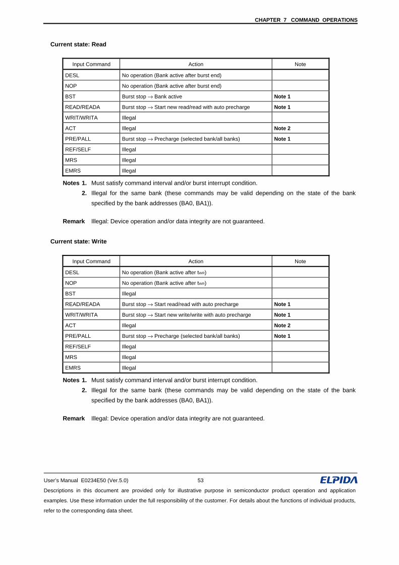
CHAPTER 7 COMMAND OPERATIONS
User’s Manual E0234E50 (Ver.5.0) 53
Descriptions in this document are provided only for illustrative purpose in semiconductor product operation and application
examples. Use these information under the full responsibility of the customer. For details about the functions of individual products,
refer to the corresponding data sheet.
Current state: Read
Input Command Action Note
DESL No operation (Bank active after burst end)
NOP No operation (Bank active after burst end)
BST Burst stop → Bank active Note 1
READ/READA Burst stop → Start new read/read with auto precharge Note 1
WRIT/WRITA Illegal
ACT Illegal Note 2
PRE/PALL Burst stop → Precharge (selected bank/all banks) Note 1
REF/SELF Illegal
MRS Illegal
EMRS Illegal
Notes 1. Must satisfy command interval and/or burst interrupt condition.
2. Illegal for the same bank (these commands may be valid depending on the state of the bank
specified by the bank addresses (BA0, BA1)).
Remark Illegal: Device operation and/or data integrity are not guaranteed.
Current state: Write
Input Command Action Note
DESL No operation (Bank active after tWR)
NOP No operation (Bank active after tWR)
BST Illegal
READ/READA Burst stop → Start read/read with auto precharge Note 1
WRIT/WRITA Burst stop → Start new write/write with auto precharge Note 1
ACT Illegal Note 2
PRE/PALL Burst stop → Precharge (selected bank/all banks) Note 1
REF/SELF Illegal
MRS Illegal
EMRS Illegal
Notes 1. Must satisfy command interval and/or burst interrupt condition.
2. Illegal for the same bank (these commands may be valid depending on the state of the bank
specified by the bank addresses (BA0, BA1)).
Remark Illegal: Device operation and/or data integrity are not guaranteed.
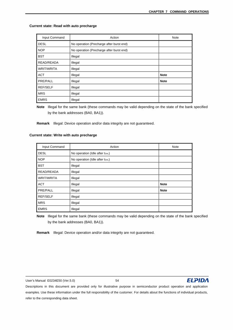
CHAPTER 7 COMMAND OPERATIONS
User’s Manual E0234E50 (Ver.5.0) 54
Descriptions in this document are provided only for illustrative purpose in semiconductor product operation and application
examples. Use these information under the full responsibility of the customer. For details about the functions of individual products,
refer to the corresponding data sheet.
Current state: Read with auto precharge
Input Command Action Note
DESL No operation (Precharge after burst end)
NOP No operation (Precharge after burst end)
BST Illegal
READ/READA Illegal
WRIT/WRITA Illegal
ACT Illegal Note
PRE/PALL Illegal Note
REF/SELF Illegal
MRS Illegal
EMRS Illegal
Note Illegal for the same bank (these commands may be valid depending on the state of the bank specified
by the bank addresses (BA0, BA1)).
Remark Illegal: Device operation and/or data integrity are not guaranteed.
Current state: Write with auto precharge
Input Command Action Note
DESL No operation (Idle after tDAL)
NOP No operation (Idle after tDAL)
BST Illegal
READ/READA Illegal
WRIT/WRITA Illegal
ACT Illegal Note
PRE/PALL Illegal Note
REF/SELF Illegal
MRS Illegal
EMRS Illegal
Note Illegal for the same bank (these commands may be valid depending on the state of the bank specified
by the bank addresses (BA0, BA1)).
Remark Illegal: Device operation and/or data integrity are not guaranteed.
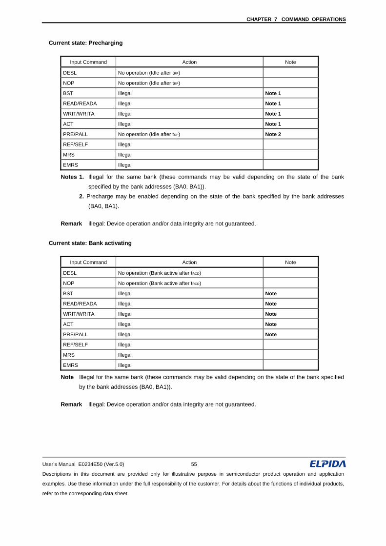
CHAPTER 7 COMMAND OPERATIONS
User’s Manual E0234E50 (Ver.5.0) 55
Descriptions in this document are provided only for illustrative purpose in semiconductor product operation and application
examples. Use these information under the full responsibility of the customer. For details about the functions of individual products,
refer to the corresponding data sheet.
Current state: Precharging
Input Command Action Note
DESL No operation (Idle after tRP)
NOP No operation (Idle after tRP)
BST Illegal Note 1
READ/READA Illegal Note 1
WRIT/WRITA Illegal Note 1
ACT Illegal Note 1
PRE/PALL No operation (Idle after tRP) Note 2
REF/SELF Illegal
MRS Illegal
EMRS Illegal
Notes 1. Illegal for the same bank (these commands may be valid depending on the state of the bank
specified by the bank addresses (BA0, BA1)). 2. Precharge may be enabled depending on the state of the bank specified by the bank addresses
(BA0, BA1). Remark Illegal: Device operation and/or data integrity are not guaranteed.
Current state: Bank activating
Input Command Action Note
DESL No operation (Bank active after tRCD)
NOP No operation (Bank active after tRCD)
BST Illegal Note
READ/READA Illegal Note
WRIT/WRITA Illegal Note
ACT Illegal Note
PRE/PALL Illegal Note
REF/SELF Illegal
MRS Illegal
EMRS Illegal
Note Illegal for the same bank (these commands may be valid depending on the state of the bank specified
by the bank addresses (BA0, BA1)). Remark Illegal: Device operation and/or data integrity are not guaranteed.
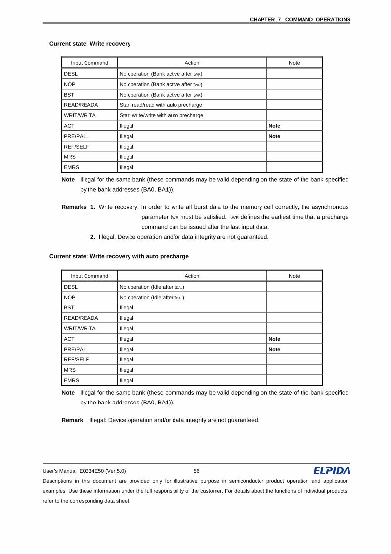
CHAPTER 7 COMMAND OPERATIONS
User’s Manual E0234E50 (Ver.5.0) 56
Descriptions in this document are provided only for illustrative purpose in semiconductor product operation and application
examples. Use these information under the full responsibility of the customer. For details about the functions of individual products,
refer to the corresponding data sheet.
Current state: Write recovery
Input Command Action Note
DESL No operation (Bank active after tWR)
NOP No operation (Bank active after tWR)
BST No operation (Bank active after tWR)
READ/READA Start read/read with auto precharge
WRIT/WRITA Start write/write with auto precharge
ACT Illegal Note
PRE/PALL Illegal Note
REF/SELF Illegal
MRS Illegal
EMRS Illegal
Note Illegal for the same bank (these commands may be valid depending on the state of the bank specified
by the bank addresses (BA0, BA1)).
Remarks 1. Write recovery: In order to write all burst data to the memory cell correctly, the asynchronous
parameter tWR must be satisfied. tWR defines the earliest time that a precharge
command can be issued after the last input data. 2. Illegal: Device operation and/or data integrity are not guaranteed.
Current state: Write recovery with auto precharge
Input Command Action Note
DESL No operation (Idle after tDAL)
NOP No operation (Idle after tDAL)
BST Illegal
READ/READA Illegal
WRIT/WRITA Illegal
ACT Illegal Note
PRE/PALL Illegal Note
REF/SELF Illegal
MRS Illegal
EMRS Illegal
Note Illegal for the same bank (these commands may be valid depending on the state of the bank specified
by the bank addresses (BA0, BA1)).
Remark Illegal: Device operation and/or data integrity are not guaranteed.
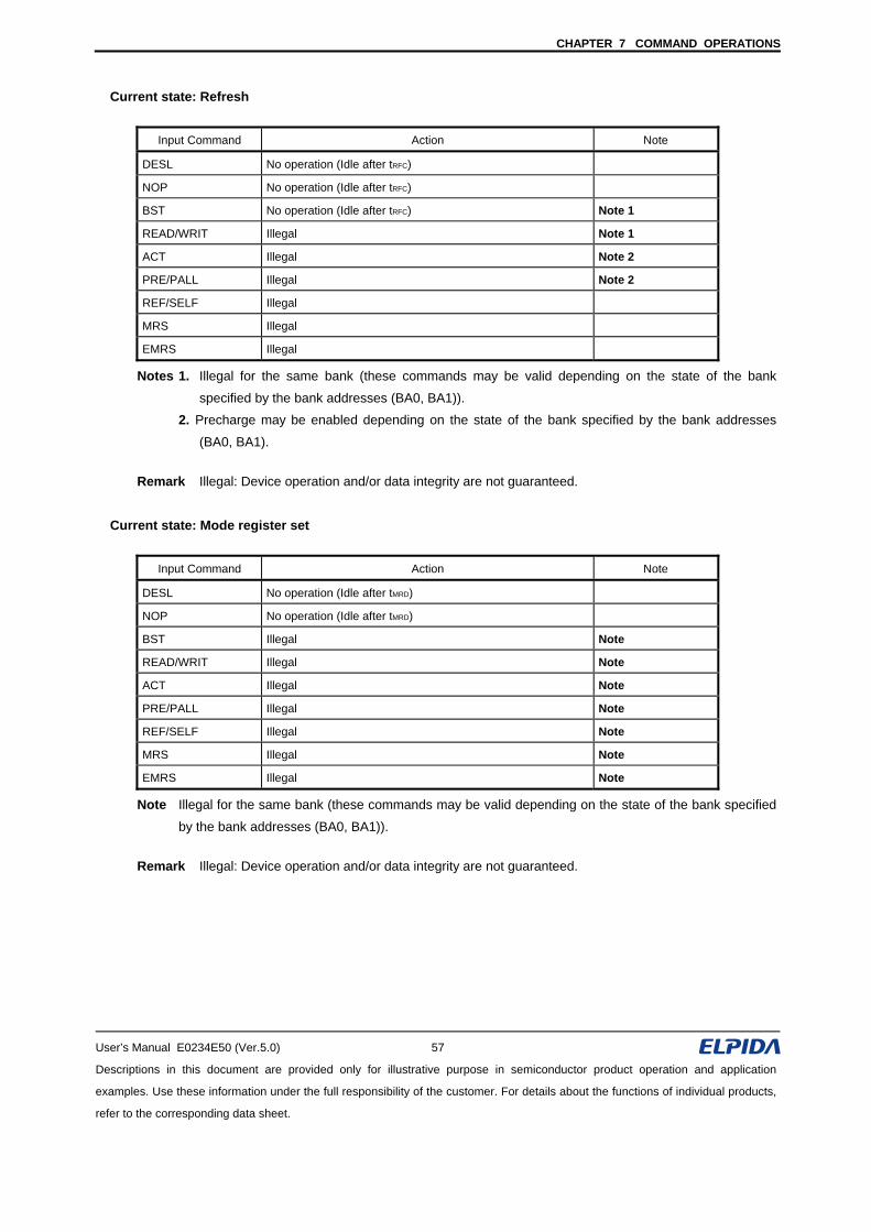
CHAPTER 7 COMMAND OPERATIONS
User’s Manual E0234E50 (Ver.5.0) 57
Descriptions in this document are provided only for illustrative purpose in semiconductor product operation and application
examples. Use these information under the full responsibility of the customer. For details about the functions of individual products,
refer to the corresponding data sheet.
Current state: Refresh
Input Command Action Note
DESL No operation (Idle after tRFC)
NOP No operation (Idle after tRFC)
BST No operation (Idle after tRFC) Note 1
READ/WRIT Illegal Note 1
ACT Illegal Note 2
PRE/PALL Illegal Note 2
REF/SELF Illegal
MRS Illegal
EMRS Illegal
Notes 1. Illegal for the same bank (these commands may be valid depending on the state of the bank
specified by the bank addresses (BA0, BA1)). 2. Precharge may be enabled depending on the state of the bank specified by the bank addresses
(BA0, BA1).
Remark Illegal: Device operation and/or data integrity are not guaranteed.
Current state: Mode register set
Input Command Action Note
DESL No operation (Idle after tMRD)
NOP No operation (Idle after tMRD)
BST Illegal Note
READ/WRIT Illegal Note
ACT Illegal Note
PRE/PALL Illegal Note
REF/SELF Illegal Note
MRS Illegal Note
EMRS Illegal Note
Note Illegal for the same bank (these commands may be valid depending on the state of the bank specified
by the bank addresses (BA0, BA1)).
Remark Illegal: Device operation and/or data integrity are not guaranteed.
CHAPTER 8 BASIC OPERATION MODES
User’s Manual E0234E50 (Ver.5.0) 58
Descriptions in this document are provided only for illustrative purpose in semiconductor product operation and application
examples. Use these information under the full responsibility of the customer. For details about the functions of individual products,
refer to the corresponding data sheet.
CHAPTER 8 BASIC OPERATION MODES
This chapter describes the three basic operation modes of DDR SDRAM:
Read mode
Write mode
Refresh mode
8.1 Read Mode
A read operation is executed by issuing the read command (READ) for an active bank. The read operation
sequence is as follows.
(1) To activate a particular row in a particular bank, the bank active command (ACT) is issued along with a row
address and bank address.
(2) After the lapse of tRCD from the ACT command, the starting column and bank addresses are provided with the
READ command.
(3) After the lapse of the /CAS latency from the READ command, the read burst data is available, starting from the
column address specified in (2). The number of successive burst data is determined by the burst length (BL).
(4) After the lapse of tRAS from the ACT command, the precharge command (PRE) is input. To output all the burst
data, the earliest timing for PRE command is (burst length/2) clocks after the READ command.
Caution The precharge command input timing (tRAS) may differ depending on the DDR SDRAM
product. For details, refer to the data sheet of each product.
(5) After the lapse of tRP, the corresponding bank becomes idle.
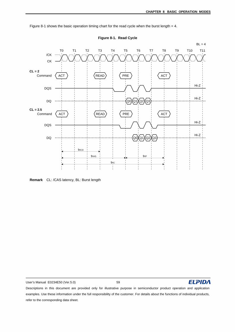
CHAPTER 8 BASIC OPERATION MODES
User’s Manual E0234E50 (Ver.5.0) 59
Descriptions in this document are provided only for illustrative purpose in semiconductor product operation and application
examples. Use these information under the full responsibility of the customer. For details about the functions of individual products,
refer to the corresponding data sheet.
Figure 8-1 shows the basic operation timing chart for the read cycle when the burst length = 4.
Figure 8-1. Read Cycle
/CK
Command
DQS
DQ
CK
T0 T1 T2 T3 T4 T5 T6 T7 T8 T9 T10 T11
Q0 Q1 Q2 Q3
DQS
DQ Q0 Q1 Q2 Q3
READ PRE ACT
ACTCommand READ PREACT
ACT
Hi-Z
Hi-Z
Hi-Z
Hi-Z
CL = 2
CL = 2.5
tRCD
tRAS
tRC
tRP
BL = 4
Remark CL: /CAS latency, BL: Burst length
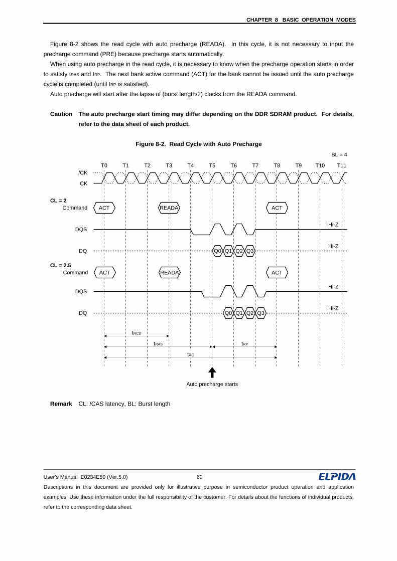
CHAPTER 8 BASIC OPERATION MODES
User’s Manual E0234E50 (Ver.5.0) 60
Descriptions in this document are provided only for illustrative purpose in semiconductor product operation and application
examples. Use these information under the full responsibility of the customer. For details about the functions of individual products,
refer to the corresponding data sheet.
Figure 8-2 shows the read cycle with auto precharge (READA). In this cycle, it is not necessary to input the
precharge command (PRE) because precharge starts automatically.
When using auto precharge in the read cycle, it is necessary to know when the precharge operation starts in order
to satisfy tRAS and tRP. The next bank active command (ACT) for the bank cannot be issued until the auto precharge
cycle is completed (until tRP is satisfied).
Auto precharge will start after the lapse of (burst length/2) clocks from the READA command.
Caution The auto precharge start timing may differ depending on the DDR SDRAM product. For details,
refer to the data sheet of each product.
Figure 8-2. Read Cycle with Auto Precharge
/CK
Command
DQS
DQ
CK
T0 T1 T2 T3 T4 T5 T6 T7 T8 T9 T10 T11
Q0 Q1 Q2 Q3
DQS
DQ Q0 Q1 Q2 Q3
READA ACT
ACTCommand READAACT
ACT
Hi-Z
Hi-Z
Hi-Z
Hi-Z
CL = 2
CL = 2.5
tRCD
tRAS
tRC
tRP
BL = 4
Auto precharge starts Remark CL: /CAS latency, BL: Burst length
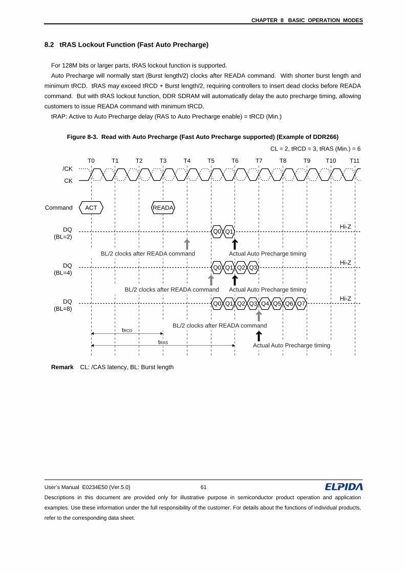
CHAPTER 8 BASIC OPERATION MODES
User’s Manual E0234E50 (Ver.5.0) 61
Descriptions in this document are provided only for illustrative purpose in semiconductor product operation and application
examples. Use these information under the full responsibility of the customer. For details about the functions of individual products,
refer to the corresponding data sheet.
8.2 tRAS Lockout Function (Fast Auto Precharge)
For 128M bits or larger parts, tRAS lockout function is supported.
Auto Precharge will normally start (Burst length/2) clocks after READA command. With shorter burst length and
minimum tRCD. tRAS may exceed tRCD + Burst length/2, requiring controllers to insert dead clocks before READA
command. But with tRAS lockout function, DDR SDRAM will automatically delay the auto precharge timing, allowing
customers to issue READA command with minimum tRCD.
tRAP: Active to Auto Precharge delay (RAS to Auto Precharge enable) = tRCD (Min.)
Figure 8-3. Read with Auto Precharge (Fast Auto Precharge supported) (Example of DDR266)
/CK
Command
DQ(BL=2)
CK
T0 T1 T2 T3 T4 T5 T6 T7 T8 T9 T10 T11
ACT
CL = 2, tRCD = 3, tRAS (Min.) = 6
READA
Hi-ZQ1Q0
DQ(BL=4)
Hi-ZQ1 Q2 Q3Q0
DQ(BL=8)
Hi-ZQ1 Q2 Q3Q0 Q5 Q6 Q7Q4
tRCD
tRAS
Actual Auto Precharge timingBL/2 clocks after READA command
BL/2 clocks after READA command
BL/2 clocks after READA command
Actual Auto Precharge timing
Actual Auto Precharge timing
Remark CL: /CAS latency, BL: Burst length
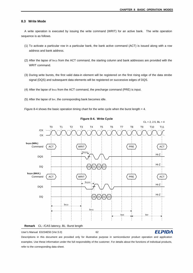
CHAPTER 8 BASIC OPERATION MODES
User’s Manual E0234E50 (Ver.5.0) 62
Descriptions in this document are provided only for illustrative purpose in semiconductor product operation and application
examples. Use these information under the full responsibility of the customer. For details about the functions of individual products,
refer to the corresponding data sheet.
8.3 Write Mode
A write operation is executed by issuing the write command (WRIT) for an active bank. The write operation
sequence is as follows.
(1) To activate a particular row in a particular bank, the bank active command (ACT) is issued along with a row
address and bank address.
(2) After the lapse of tRCD from the ACT command, the starting column and bank addresses are provided with the
WRIT command.
(3) During write bursts, the first valid data-in element will be registered on the first rising edge of the data strobe
signal (DQS) and subsequent data elements will be registered on successive edges of DQS.
(4) After the lapse of tRAS from the ACT command, the precharge command (PRE) is input.
(5) After the lapse of tRP, the corresponding bank becomes idle.
Figure 8-4 shows the basic operation timing chart for the write cycle when the burst length = 4.
Figure 8-4. Write Cycle
/CK
Command
DQS
DQ
CK
T0 T1 T2 T3 T4 T5 T6 T7 T8 T9 T10 T11
PRE ACTACT
CL = 2, 2.5, BL = 4
Hi-Z
WRIT
Hi-ZD1 D2 D3
tDQSS
tDQSS (MIN.)
Command PRE ACTACT WRITtDQSS (MAX.)
D0
DQS
DQ
tWR tRP
Hi-Z
Hi-ZD1 D2 D3
tRCD
tRAS
tDQSS
D0
Remark CL: /CAS latency, BL: Burst length
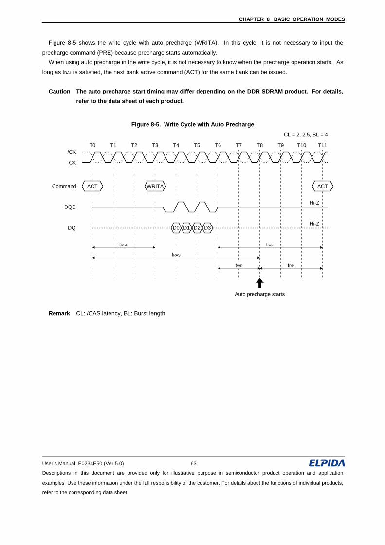
CHAPTER 8 BASIC OPERATION MODES
User’s Manual E0234E50 (Ver.5.0) 63
Descriptions in this document are provided only for illustrative purpose in semiconductor product operation and application
examples. Use these information under the full responsibility of the customer. For details about the functions of individual products,
refer to the corresponding data sheet.
Figure 8-5 shows the write cycle with auto precharge (WRITA). In this cycle, it is not necessary to input the
precharge command (PRE) because precharge starts automatically.
When using auto precharge in the write cycle, it is not necessary to know when the precharge operation starts. As
long as tDAL is satisfied, the next bank active command (ACT) for the same bank can be issued.
Caution The auto precharge start timing may differ depending on the DDR SDRAM product. For details,
refer to the data sheet of each product.
Figure 8-5. Write Cycle with Auto Precharge
/CK
Command
DQS
DQ
CK
T0 T1 T2 T3 T4 T5 T6 T7 T8 T9 T10 T11
ACTACT
tWR tRP
tDAL
CL = 2, 2.5, BL = 4
Hi-Z
WRITA
Hi-ZD0 D1 D2 D3
tRCD
tRAS
Auto precharge starts
Remark CL: /CAS latency, BL: Burst length
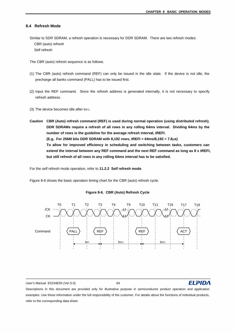
CHAPTER 8 BASIC OPERATION MODES
User’s Manual E0234E50 (Ver.5.0) 64
Descriptions in this document are provided only for illustrative purpose in semiconductor product operation and application
examples. Use these information under the full responsibility of the customer. For details about the functions of individual products,
refer to the corresponding data sheet.
8.4 Refresh Mode
Similar to SDR SDRAM, a refresh operation is necessary for DDR SDRAM. There are two refresh modes:
CBR (auto) refresh
Self refresh
The CBR (auto) refresh sequence is as follows.
(1) The CBR (auto) refresh command (REF) can only be issued in the idle state. If the device is not idle, the
precharge all banks command (PALL) has to be issued first.
(2) Input the REF command. Since the refresh address is generated internally, it is not necessary to specify
refresh address.
(3) The device becomes idle after tRFC.
Caution CBR (Auto) refresh command (REF) is used during normal operation (using distributed refresh).
DDR SDRAMs require a refresh of all rows in any rolling 64ms interval. Dividing 64ms by the number of rows is the guideline for the average refresh interval, tREFI.
(E.g. For 256M bits DDR SDRAM with 8,192 rows, tREFI = 64ms/8,192 = 7.8μs) To allow for improved efficiency in scheduling and switching between tasks, customers can
extend the interval between any REF command and the next REF command as long as 8 x tREFI, but still refresh of all rows in any rolling 64ms interval has to be satisfied.
For the self refresh mode operation, refer to 11.2.2 Self refresh mode.
Figure 8-6 shows the basic operation timing chart for the CBR (auto) refresh cycle.
Figure 8-6. CBR (Auto) Refresh Cycle
Command PALL REF REF ACT
/CK
CK
T0 T1 T2 T3 T4 T9 T10 T11 T16 T17 T18
tRP tRFC tRFC
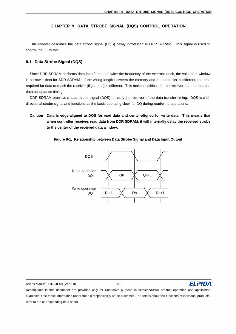
CHAPTER 9 DATA STROBE SIGNAL (DQS) CONTROL OPERATION
User’s Manual E0234E50 (Ver.5.0) 65
Descriptions in this document are provided only for illustrative purpose in semiconductor product operation and application
examples. Use these information under the full responsibility of the customer. For details about the functions of individual products,
refer to the corresponding data sheet.
CHAPTER 9 DATA STROBE SIGNAL (DQS) CONTROL OPERATION
This chapter describes the data strobe signal (DQS) newly introduced in DDR SDRAM. This signal is used to
control the I/O buffer.
9.1 Data Strobe Signal (DQS)
Since DDR SDRAM performs data input/output at twice the frequency of the external clock, the valid data window
is narrower than for SDR SDRAM. If the wiring length between the memory and the controller is different, the time
required for data to reach the receiver (flight time) is different. This makes it difficult for the receiver to determine the
data acceptance timing.
DDR SDRAM employs a data strobe signal (DQS) to notify the receiver of the data transfer timing. DQS is a bi-
directional strobe signal and functions as the basic operating clock for DQ during read/write operations.
Cantion Data is edge-aligned to DQS for read data and center-aligned for write data. This means that
when controller receives read data from DDR SDRAM, it will internally delay the received strobe to the center of the received data window.
Figure 9-1. Relationship between Data Strobe Signal and Data Input/Output
DQS
DQ
DQ
Read operation
Write operation
Qn Qn+1
DnDn-1 Dn+1
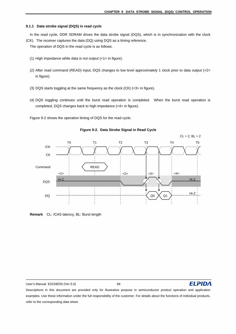
CHAPTER 9 DATA STROBE SIGNAL (DQS) CONTROL OPERATION
User’s Manual E0234E50 (Ver.5.0) 66
Descriptions in this document are provided only for illustrative purpose in semiconductor product operation and application
examples. Use these information under the full responsibility of the customer. For details about the functions of individual products,
refer to the corresponding data sheet.
9.1.1 Data strobe signal (DQS) in read cycle
In the read cycle, DDR SDRAM drives the data strobe signal (DQS), which is in synchronization with the clock
(CK). The receiver captures the data (DQ) using DQS as a timing reference.
The operation of DQS in the read cycle is as follows.
(1) High impedance while data is not output (<1> in figure).
(2) After read command (READ) input, DQS changes to low level approximately 1 clock prior to data output (<2>
in figure).
(3) DQS starts toggling at the same frequency as the clock (CK) (<3> in figure).
(4) DQS toggling continues until the burst read operation is completed. When the burst read operation is
completed, DQS changes back to high impedance (<4> in figure).
Figure 9-2 shows the operation timing of DQS for the read cycle.
Figure 9-2. Data Strobe Signal in Read Cycle
<3><2>
/CK
Command
DQS
CL = 2, BL = 2
READ
DQHi-Z
CK
T0 T1 T2 T3 T4 T5
Q0 Q1
Hi-Z
<1>
Hi-Z
<4>
Remark CL: /CAS latency, BL: Burst length
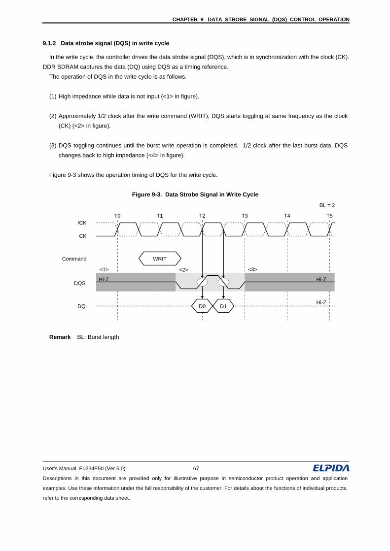
CHAPTER 9 DATA STROBE SIGNAL (DQS) CONTROL OPERATION
User’s Manual E0234E50 (Ver.5.0) 67
Descriptions in this document are provided only for illustrative purpose in semiconductor product operation and application
examples. Use these information under the full responsibility of the customer. For details about the functions of individual products,
refer to the corresponding data sheet.
9.1.2 Data strobe signal (DQS) in write cycle
In the write cycle, the controller drives the data strobe signal (DQS), which is in synchronization with the clock (CK).
DDR SDRAM captures the data (DQ) using DQS as a timing reference.
The operation of DQS in the write cycle is as follows.
(1) High impedance while data is not input (<1> in figure).
(2) Approximately 1/2 clock after the write command (WRIT), DQS starts toggling at same frequency as the clock
(CK) (<2> in figure).
(3) DQS toggling continues until the burst write operation is completed. 1/2 clock after the last burst data, DQS
changes back to high impedance (<4> in figure).
Figure 9-3 shows the operation timing of DQS for the write cycle.
Figure 9-3. Data Strobe Signal in Write Cycle
<2>
/CK
Command
DQS
BL = 2
WRIT
DQHi-Z
CK
T0 T1 T2 T3 T4 T5
D0 D1
Hi-Z
<1>
Hi-Z
<3>
Remark BL: Burst length
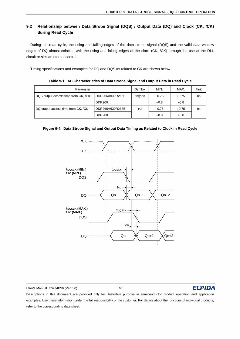
CHAPTER 9 DATA STROBE SIGNAL (DQS) CONTROL OPERATION
User’s Manual E0234E50 (Ver.5.0) 68
Descriptions in this document are provided only for illustrative purpose in semiconductor product operation and application
examples. Use these information under the full responsibility of the customer. For details about the functions of individual products,
refer to the corresponding data sheet.
9.2 Relationship between Data Strobe Signal (DQS) / Output Data (DQ) and Clock (CK, /CK) during Read Cycle
During the read cycle, the rising and falling edges of the data strobe signal (DQS) and the valid data window
edges of DQ almost coincide with the rising and falling edges of the clock (CK, /CK) through the use of the DLL
circuit or similar internal control.
Timing specifications and examples for DQ and DQS as related to CK are shown below.
Table 9-1. AC Characteristics of Data Strobe Signal and Output Data in Read Cycle
Parameter Symbol MIN. MAX. Unit
DQS output access time from CK, /CK DDR266A/DDR266B tDQSCK −0.75 +0.75 ns
DDR200 −0.8 +0.8
DQ output access time from CK, /CK DDR266A/DDR266B tAC −0.75 +0.75 ns
DDR200 −0.8 +0.8
Figure 9-4. Data Strobe Signal and Output Data Timing as Related to Clock in Read Cycle
/CK
DQS
DQ
CK
Qn Qn+1 Qn+2
Qn Qn+1 Qn+2
tAC
tDQSCKtDQSCK (MIN.)tAC (MIN.)
tDQSCK (MAX.)tAC (MAX.)
DQS
DQ
tAC
tDQSCK
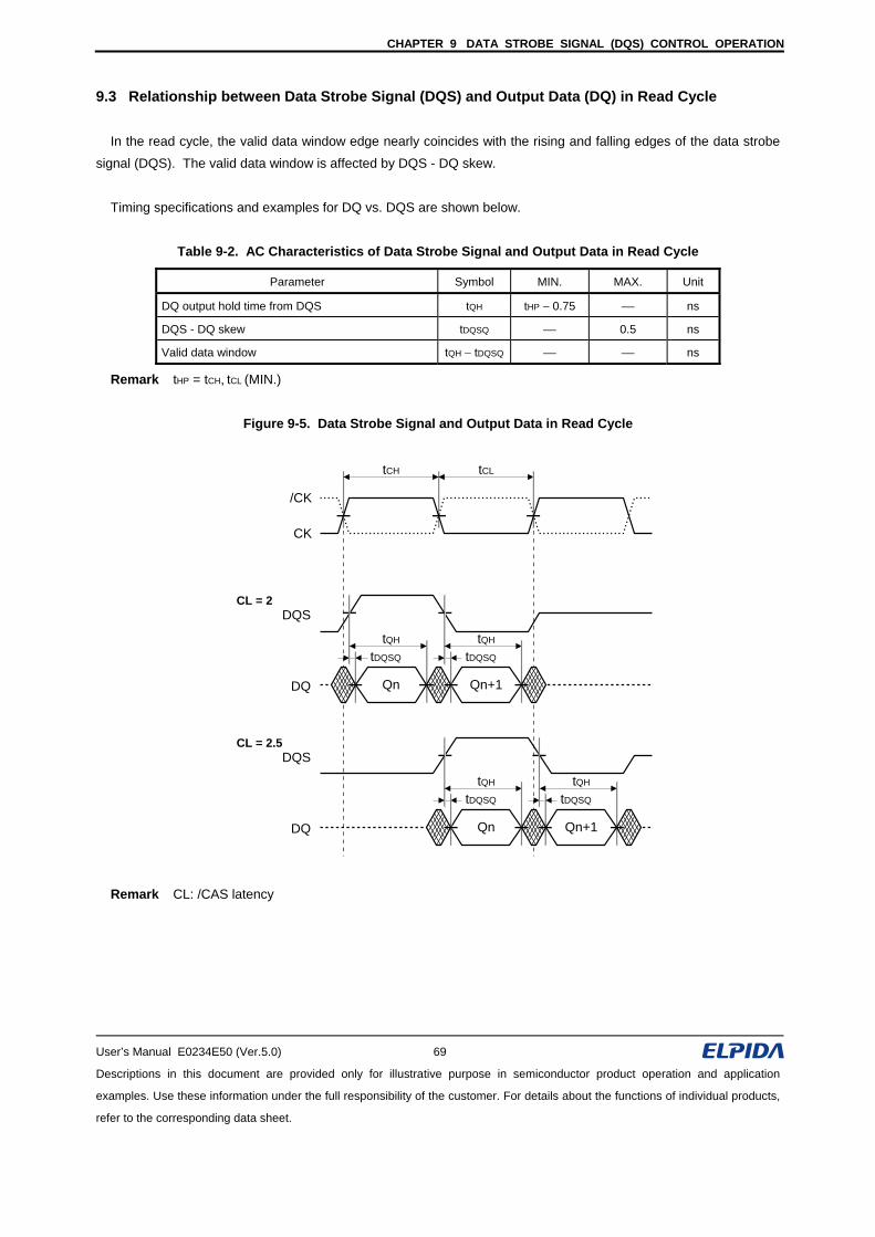
CHAPTER 9 DATA STROBE SIGNAL (DQS) CONTROL OPERATION
User’s Manual E0234E50 (Ver.5.0) 69
Descriptions in this document are provided only for illustrative purpose in semiconductor product operation and application
examples. Use these information under the full responsibility of the customer. For details about the functions of individual products,
refer to the corresponding data sheet.
9.3 Relationship between Data Strobe Signal (DQS) and Output Data (DQ) in Read Cycle
In the read cycle, the valid data window edge nearly coincides with the rising and falling edges of the data strobe
signal (DQS). The valid data window is affected by DQS - DQ skew.
Timing specifications and examples for DQ vs. DQS are shown below.
Table 9-2. AC Characteristics of Data Strobe Signal and Output Data in Read Cycle
Parameter Symbol MIN. MAX. Unit
DQ output hold time from DQS tQH tHP − 0.75 ⎯ ns
DQS - DQ skew tDQSQ ⎯ 0.5 ns
Valid data window tQH − tDQSQ ⎯ ⎯ ns
Remark tHP = tCH, tCL (MIN.)
Figure 9-5. Data Strobe Signal and Output Data in Read Cycle
tCH tCL
/CK
CK
DQS
DQ
DQS
DQ
Qn Qn+1
tDQSQ
CL = 2
tQH
CL = 2.5
tDQSQ
tQH
Qn Qn+1
tDQSQ
tQH
tDQSQ
tQH
Remark CL: /CAS latency
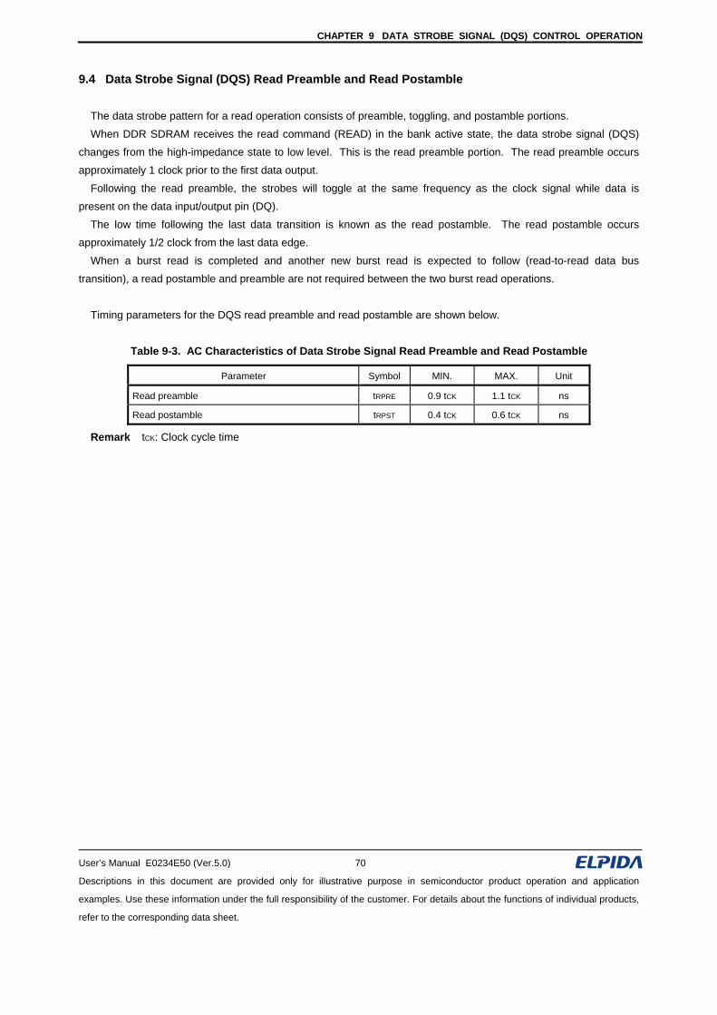
CHAPTER 9 DATA STROBE SIGNAL (DQS) CONTROL OPERATION
User’s Manual E0234E50 (Ver.5.0) 70
Descriptions in this document are provided only for illustrative purpose in semiconductor product operation and application
examples. Use these information under the full responsibility of the customer. For details about the functions of individual products,
refer to the corresponding data sheet.
9.4 Data Strobe Signal (DQS) Read Preamble and Read Postamble
The data strobe pattern for a read operation consists of preamble, toggling, and postamble portions.
When DDR SDRAM receives the read command (READ) in the bank active state, the data strobe signal (DQS)
changes from the high-impedance state to low level. This is the read preamble portion. The read preamble occurs
approximately 1 clock prior to the first data output.
Following the read preamble, the strobes will toggle at the same frequency as the clock signal while data is
present on the data input/output pin (DQ).
The low time following the last data transition is known as the read postamble. The read postamble occurs
approximately 1/2 clock from the last data edge.
When a burst read is completed and another new burst read is expected to follow (read-to-read data bus
transition), a read postamble and preamble are not required between the two burst read operations.
Timing parameters for the DQS read preamble and read postamble are shown below.
Table 9-3. AC Characteristics of Data Strobe Signal Read Preamble and Read Postamble
Parameter Symbol MIN. MAX. Unit
Read preamble tRPRE 0.9 tCK 1.1 tCK ns
Read postamble tRPST 0.4 tCK 0.6 tCK ns
Remark tCK: Clock cycle time
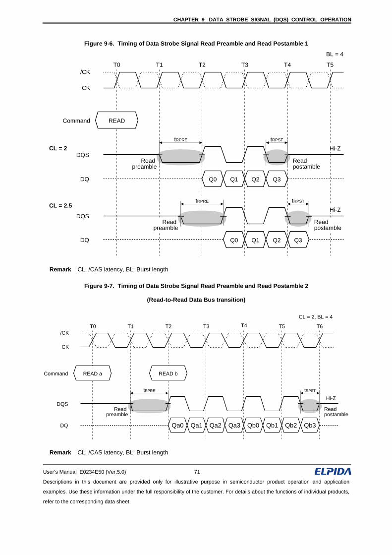
CHAPTER 9 DATA STROBE SIGNAL (DQS) CONTROL OPERATION
User’s Manual E0234E50 (Ver.5.0) 71
Descriptions in this document are provided only for illustrative purpose in semiconductor product operation and application
examples. Use these information under the full responsibility of the customer. For details about the functions of individual products,
refer to the corresponding data sheet.
Figure 9-6. Timing of Data Strobe Signal Read Preamble and Read Postamble 1
/CK
DQS
DQ
CK
Command
T0 T1 T2 T3 T4 T5
DQS
DQ
CL = 2
CL = 2.5
Hi-Z
Hi-Z
Q0 Q1 Q2 Q3
Q0 Q1 Q2 Q3
READ
tRPRE tRPST
tRPSTtRPRE
Read preamble
Read preamble
Read postamble
Read postamble
BL = 4
Remark CL: /CAS latency, BL: Burst length
Figure 9-7. Timing of Data Strobe Signal Read Preamble and Read Postamble 2
(Read-to-Read Data Bus transition)
/CK
DQS
DQ
CK
T0 T1 T2 T3 T4 T5 T6
Hi-Z
Qa0 Qa1 Qa2 Qa3 Qb0 Qb1 Qb2 Qb3
READ a READ b
tRPRE tRPST
Read preamble
Read postamble
CL = 2, BL = 4
Command
Remark CL: /CAS latency, BL: Burst length
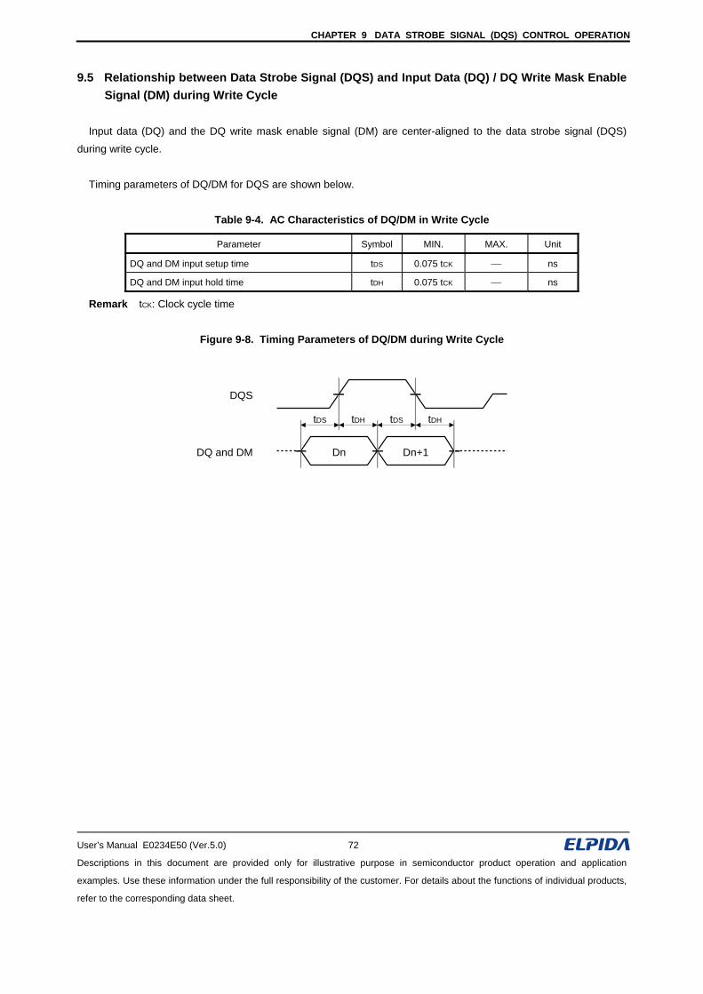
CHAPTER 9 DATA STROBE SIGNAL (DQS) CONTROL OPERATION
User’s Manual E0234E50 (Ver.5.0) 72
Descriptions in this document are provided only for illustrative purpose in semiconductor product operation and application
examples. Use these information under the full responsibility of the customer. For details about the functions of individual products,
refer to the corresponding data sheet.
9.5 Relationship between Data Strobe Signal (DQS) and Input Data (DQ) / DQ Write Mask Enable Signal (DM) during Write Cycle
Input data (DQ) and the DQ write mask enable signal (DM) are center-aligned to the data strobe signal (DQS)
during write cycle.
Timing parameters of DQ/DM for DQS are shown below.
Table 9-4. AC Characteristics of DQ/DM in Write Cycle
Parameter Symbol MIN. MAX. Unit
DQ and DM input setup time tDS 0.075 tCK ⎯ ns
DQ and DM input hold time tDH 0.075 tCK ⎯ ns
Remark tCK: Clock cycle time
Figure 9-8. Timing Parameters of DQ/DM during Write Cycle
DQS
DQ and DM Dn Dn+1
tDS tDH tDS tDH
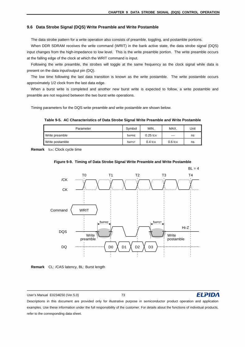
CHAPTER 9 DATA STROBE SIGNAL (DQS) CONTROL OPERATION
User’s Manual E0234E50 (Ver.5.0) 73
Descriptions in this document are provided only for illustrative purpose in semiconductor product operation and application
examples. Use these information under the full responsibility of the customer. For details about the functions of individual products,
refer to the corresponding data sheet.
9.6 Data Strobe Signal (DQS) Write Preamble and Write Postamble
The data strobe pattern for a write operation also consists of preamble, toggling, and postamble portions.
When DDR SDRAM receives the write command (WRIT) in the bank active state, the data strobe signal (DQS)
input changes from the high-impedance to low level. This is the write preamble portion. The write preamble occurs
at the falling edge of the clock at which the WRIT command is input.
Following the write preamble, the strobes will toggle at the same frequency as the clock signal while data is
present on the data input/output pin (DQ).
The low time following the last data transition is known as the write postamble. The write postamble occurs
approximately 1/2 clock from the last data edge.
When a burst write is completed and another new burst write is expected to follow, a write postamble and
preamble are not required between the two burst write operations.
Timing parameters for the DQS write preamble and write postamble are shown below.
Table 9-5. AC Characteristics of Data Strobe Signal Write Preamble and Write Postamble
Parameter Symbol MIN. MAX. Unit
Write preamble tWPRE 0.25 tCK ⎯ ns
Write postamble tWPST 0.4 tCK 0.6 tCK ns
Remark tCK: Clock cycle time
Figure 9-9. Timing of Data Strobe Signal Write Preamble and Write Postamble
/CK
DQS
DQ
CK
T0 T1 T2 T3 T4
Hi-Z
D0 D1 D2 D3
WRIT
tWPSTtWPRE
Write preamble
Write postamble
BL = 4
Command
Remark CL: /CAS latency, BL: Burst length
CHAPTER 10 DQ WRITE MASK ENABLE SIGNAL (DM) CONTROL OPERATION
User’s Manual E0234E50 (Ver.5.0) 74
Descriptions in this document are provided only for illustrative purpose in semiconductor product operation and application
examples. Use these information under the full responsibility of the customer. For details about the functions of individual products,
refer to the corresponding data sheet.
CHAPTER 10 DQ WRITE MASK ENABLE SIGNAL (DM) CONTROL OPERATION
This chapter describes DQ write mask enable signal (DM) control. DM masks input data.
Unlike SDR SDRAM, data masking is only available in the write cycle for DDR SDRAM. The burst stop command
(BST) is available during burst read, but burst stop during write is illegal. Data masking is available during write, but
data masking during read is not available.
10.1 DQ Write Mask Enable Signal (DM)
DQ pins controlled by the DQ write mask enable signal (DM) differ depending on the bit organization.
(1) ×4-bit organization
DM controls DQ0 through DQ3.
(2) ×8-bit organization
DM controls DQ0 through DQ7.
(3) ×16-bit organization
LDM controls DQ0 through DQ7 (lower bit control).
UDM controls DQ8 through DQ15 (upper bit control).
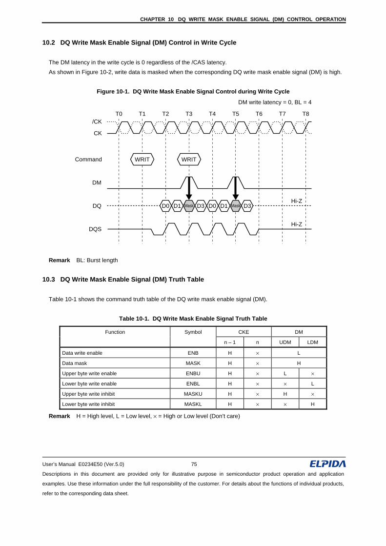
CHAPTER 10 DQ WRITE MASK ENABLE SIGNAL (DM) CONTROL OPERATION
User’s Manual E0234E50 (Ver.5.0) 75
Descriptions in this document are provided only for illustrative purpose in semiconductor product operation and application
examples. Use these information under the full responsibility of the customer. For details about the functions of individual products,
refer to the corresponding data sheet.
10.2 DQ Write Mask Enable Signal (DM) Control in Write Cycle
The DM latency in the write cycle is 0 regardless of the /CAS latency.
As shown in Figure 10-2, write data is masked when the corresponding DQ write mask enable signal (DM) is high.
Figure 10-1. DQ Write Mask Enable Signal Control during Write Cycle
/CK
Command
DM
DM write latency = 0, BL = 4
WRIT
DQHi-Z
CK
T0 T1 T2 T3 T4 T5 T6 T7 T8
D0 D1 D3
DQS
D0 D1 D3Mask Mask
Hi-Z
WRIT
Remark BL: Burst length
10.3 DQ Write Mask Enable Signal (DM) Truth Table
Table 10-1 shows the command truth table of the DQ write mask enable signal (DM).
Table 10-1. DQ Write Mask Enable Signal Truth Table
Function Symbol CKE DM
n – 1 n UDM LDM
Data write enable ENB H × L
Data mask MASK H × H
Upper byte write enable ENBU H × L ×
Lower byte write enable ENBL H × × L
Upper byte write inhibit MASKU H × H ×
Lower byte write inhibit MASKL H × × H
Remark H = High level, L = Low level, × = High or Low level (Don’t care)
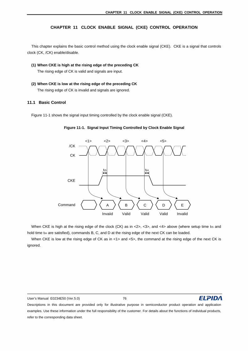
CHAPTER 11 CLOCK ENABLE SIGNAL (CKE) CONTROL OPERATION
User’s Manual E0234E50 (Ver.5.0) 76
Descriptions in this document are provided only for illustrative purpose in semiconductor product operation and application
examples. Use these information under the full responsibility of the customer. For details about the functions of individual products,
refer to the corresponding data sheet.
CHAPTER 11 CLOCK ENABLE SIGNAL (CKE) CONTROL OPERATION
This chapter explains the basic control method using the clock enable signal (CKE). CKE is a signal that controls
clock (CK, /CK) enable/disable.
(1) When CKE is high at the rising edge of the preceding CK
The rising edge of CK is valid and signals are input.
(2) When CKE is low at the rising edge of the preceding CK
The rising edge of CK is invalid and signals are ignored.
11.1 Basic Control
Figure 11-1 shows the signal input timing controlled by the clock enable signal (CKE).
Figure 11-1. Signal Input Timing Controlled by Clock Enable Signal
/CK
CKE
Command A B C D E
CK
<1> <2> <3> <4> <5>
Invaiid InvalidValid ValidValid
tIS tIH
When CKE is high at the rising edge of the clock (CK) as in <2>, <3>, and <4> above (where setup time tIS and
hold time tIH are satisfied), commands B, C, and D at the rising edge of the next CK can be loaded.
When CKE is low at the rising edge of CK as in <1> and <5>, the command at the rising edge of the next CK is
ignored.
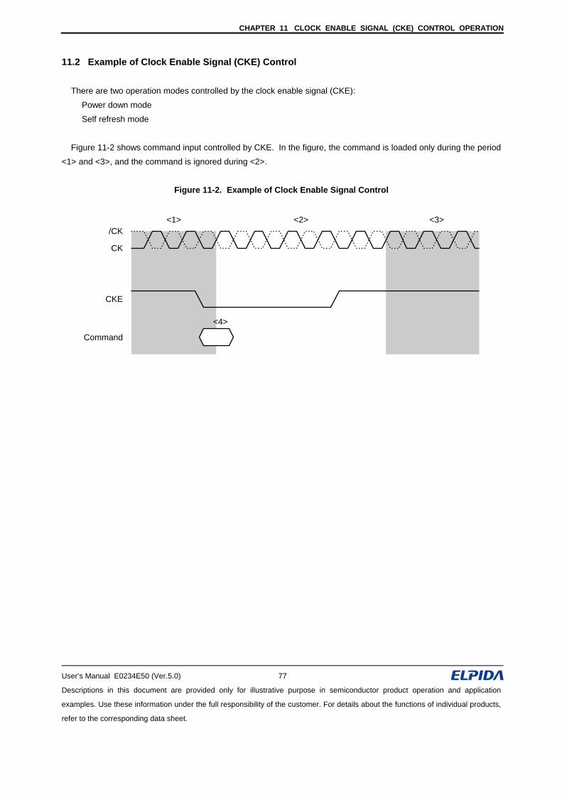
CHAPTER 11 CLOCK ENABLE SIGNAL (CKE) CONTROL OPERATION
User’s Manual E0234E50 (Ver.5.0) 77
Descriptions in this document are provided only for illustrative purpose in semiconductor product operation and application
examples. Use these information under the full responsibility of the customer. For details about the functions of individual products,
refer to the corresponding data sheet.
11.2 Example of Clock Enable Signal (CKE) Control
There are two operation modes controlled by the clock enable signal (CKE):
Power down mode
Self refresh mode
Figure 11-2 shows command input controlled by CKE. In the figure, the command is loaded only during the period
<1> and <3>, and the command is ignored during <2>.
Figure 11-2. Example of Clock Enable Signal Control
/CK
CKE
Command
CK
<1> <2> <3>
<4>
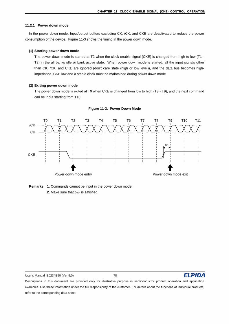
CHAPTER 11 CLOCK ENABLE SIGNAL (CKE) CONTROL OPERATION
User’s Manual E0234E50 (Ver.5.0) 78
Descriptions in this document are provided only for illustrative purpose in semiconductor product operation and application
examples. Use these information under the full responsibility of the customer. For details about the functions of individual products,
refer to the corresponding data sheet.
11.2.1 Power down mode
In the power down mode, Input/output buffers excluding CK, /CK, and CKE are deactivated to reduce the power
consumption of the device. Figure 11-3 shows the timing in the power down mode.
(1) Starting power down mode
The power down mode is started at T2 when the clock enable signal (CKE) is changed from high to low (T1 -
T2) in the all banks idle or bank active state. When power down mode is started, all the input signals other
than CK, /CK, and CKE are ignored (don’t care state (high or low level)), and the data bus becomes high-
impedance. CKE low and a stable clock must be maintained during power down mode.
(2) Exiting power down mode
The power down mode is exited at T9 when CKE is changed from low to high (T8 - T9), and the next command
can be input starting from T10.
Figure 11-3. Power Down Mode
/CK
CKE
CK
Power down mode entry Power down mode exit
T0 T1 T2 T3 T4 T5 T6 T7 T8 T9 T10 T11
tIS
Remarks 1. Commands cannot be input in the power down mode.
2. Make sure that tREF is satisfied.
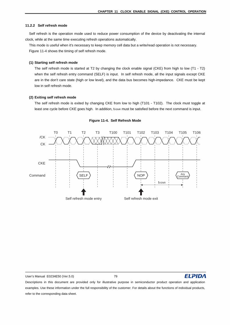
CHAPTER 11 CLOCK ENABLE SIGNAL (CKE) CONTROL OPERATION
User’s Manual E0234E50 (Ver.5.0) 79
Descriptions in this document are provided only for illustrative purpose in semiconductor product operation and application
examples. Use these information under the full responsibility of the customer. For details about the functions of individual products,
refer to the corresponding data sheet.
11.2.2 Self refresh mode
Self refresh is the operation mode used to reduce power consumption of the device by deactivating the internal
clock, while at the same time executing refresh operations automatically.
This mode is useful when it's necessary to keep memory cell data but a write/read operation is not necessary.
Figure 11-4 shows the timing of self refresh mode.
(1) Starting self refresh mode
The self refresh mode is started at T2 by changing the clock enable signal (CKE) from high to low (T1 - T2)
when the self refresh entry command (SELF) is input. In self refresh mode, all the input signals except CKE
are in the don’t care state (high or low level), and the data bus becomes high-impedance. CKE must be kept
low in self refresh mode.
(2) Exiting self refresh mode
The self refresh mode is exited by changing CKE from low to high (T101 - T102). The clock must toggle at
least one cycle before CKE goes high. In addition, tXSNR must be satisfied before the next command is input.
Figure 11-4. Self Refresh Mode
Command
/CK
CKE
CK
Self refresh mode entry Self refresh mode exit
T0 T1 T2 T3 T100 T101 T102 T103 T104 T105 T106
SELF NOP AnyCommand
tXSNR
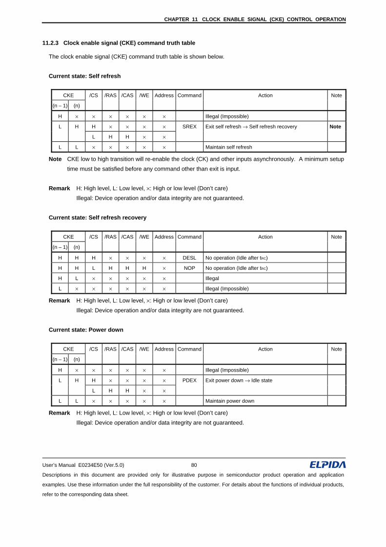
CHAPTER 11 CLOCK ENABLE SIGNAL (CKE) CONTROL OPERATION
User’s Manual E0234E50 (Ver.5.0) 80
Descriptions in this document are provided only for illustrative purpose in semiconductor product operation and application
examples. Use these information under the full responsibility of the customer. For details about the functions of individual products,
refer to the corresponding data sheet.
11.2.3 Clock enable signal (CKE) command truth table
The clock enable signal (CKE) command truth table is shown below.
Current state: Self refresh
CKE /CS /RAS /CAS /WE Address Command Action Note
(n – 1) (n)
H × × × × × × Illegal (Impossible)
L H H × × × × SREX Exit self refresh → Self refresh recovery Note
L H H × ×
L L × × × × × Maintain self refresh
Note CKE low to high transition will re-enable the clock (CK) and other inputs asynchronously. A minimum setup
time must be satisfied before any command other than exit is input.
Remark H: High level, L: Low level, ×: High or low level (Don’t care)
Illegal: Device operation and/or data integrity are not guaranteed.
Current state: Self refresh recovery
CKE /CS /RAS /CAS /WE Address Command Action Note
(n – 1) (n)
H H H × × × × DESL No operation (Idle after tRC)
H H L H H H × NOP No operation (Idle after tRC)
H L × × × × × Illegal
L × × × × × × Illegal (Impossible)
Remark H: High level, L: Low level, ×: High or low level (Don’t care)
Illegal: Device operation and/or data integrity are not guaranteed.
Current state: Power down
CKE /CS /RAS /CAS /WE Address Command Action Note
(n – 1) (n)
H × × × × × × Illegal (Impossible)
L H H × × × × PDEX Exit power down → Idle state
L H H × ×
L L × × × × × Maintain power down
Remark H: High level, L: Low level, ×: High or low level (Don’t care)
Illegal: Device operation and/or data integrity are not guaranteed.
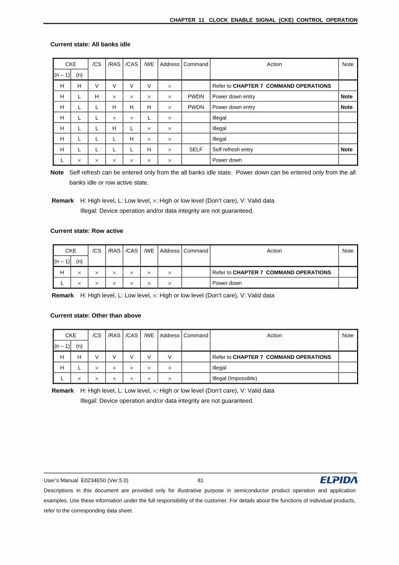
CHAPTER 11 CLOCK ENABLE SIGNAL (CKE) CONTROL OPERATION
User’s Manual E0234E50 (Ver.5.0) 81
Descriptions in this document are provided only for illustrative purpose in semiconductor product operation and application
examples. Use these information under the full responsibility of the customer. For details about the functions of individual products,
refer to the corresponding data sheet.
Current state: All banks idle
CKE /CS /RAS /CAS /WE Address Command Action Note
(n – 1) (n)
H H V V V V × Refer to CHAPTER 7 COMMAND OPERATIONS
H L H × × × × PWDN Power down entry Note
H L L H H H × PWDN Power down entry Note
H L L × × L × Illegal
H L L H L × × Illegal
H L L L H × × Illegal
H L L L L H × SELF Self refresh entry Note
L × × × × × × Power down
Note Self refresh can be entered only from the all banks idle state. Power down can be entered only from the all
banks idle or row active state. Remark H: High level, L: Low level, ×: High or low level (Don’t care), V: Valid data
Illegal: Device operation and/or data integrity are not guaranteed.
Current state: Row active
CKE /CS /RAS /CAS /WE Address Command Action Note
(n – 1) (n)
H × × × × × × Refer to CHAPTER 7 COMMAND OPERATIONS
L × × × × × × Power down
Remark H: High level, L: Low level, ×: High or low level (Don’t care), V: Valid data
Current state: Other than above
CKE /CS /RAS /CAS /WE Address Command Action Note
(n – 1) (n)
H H V V V V V Refer to CHAPTER 7 COMMAND OPERATIONS
H L × × × × × Illegal
L × × × × × × Illegal (Impossible)
Remark H: High level, L: Low level, ×: High or low level (Don’t care), V: Valid data
Illegal: Device operation and/or data integrity are not guaranteed.
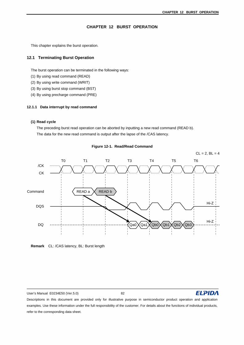
CHAPTER 12 BURST OPERATION
User’s Manual E0234E50 (Ver.5.0) 82
Descriptions in this document are provided only for illustrative purpose in semiconductor product operation and application
examples. Use these information under the full responsibility of the customer. For details about the functions of individual products,
refer to the corresponding data sheet.
CHAPTER 12 BURST OPERATION
This chapter explains the burst operation.
12.1 Terminating Burst Operation
The burst operation can be terminated in the following ways:
(1) By using read command (READ)
(2) By using write command (WRIT)
(3) By using burst stop command (BST)
(4) By using precharge command (PRE)
12.1.1 Data interrupt by read command
(1) Read cycle
The preceding burst read operation can be aborted by inputting a new read command (READ b).
The data for the new read command is output after the lapse of the /CAS latency.
Figure 12-1. Read/Read Command
/CK
Command
DQ
CK
T0 T1 T2 T3 T4 T5 T6
Qa0 Qa1 Qb0 Qb1 Qb2 Qb3Hi-Z
Hi-Z
CL = 2, BL = 4
DQS
READ bREAD a
Remark CL: /CAS latency, BL: Burst length
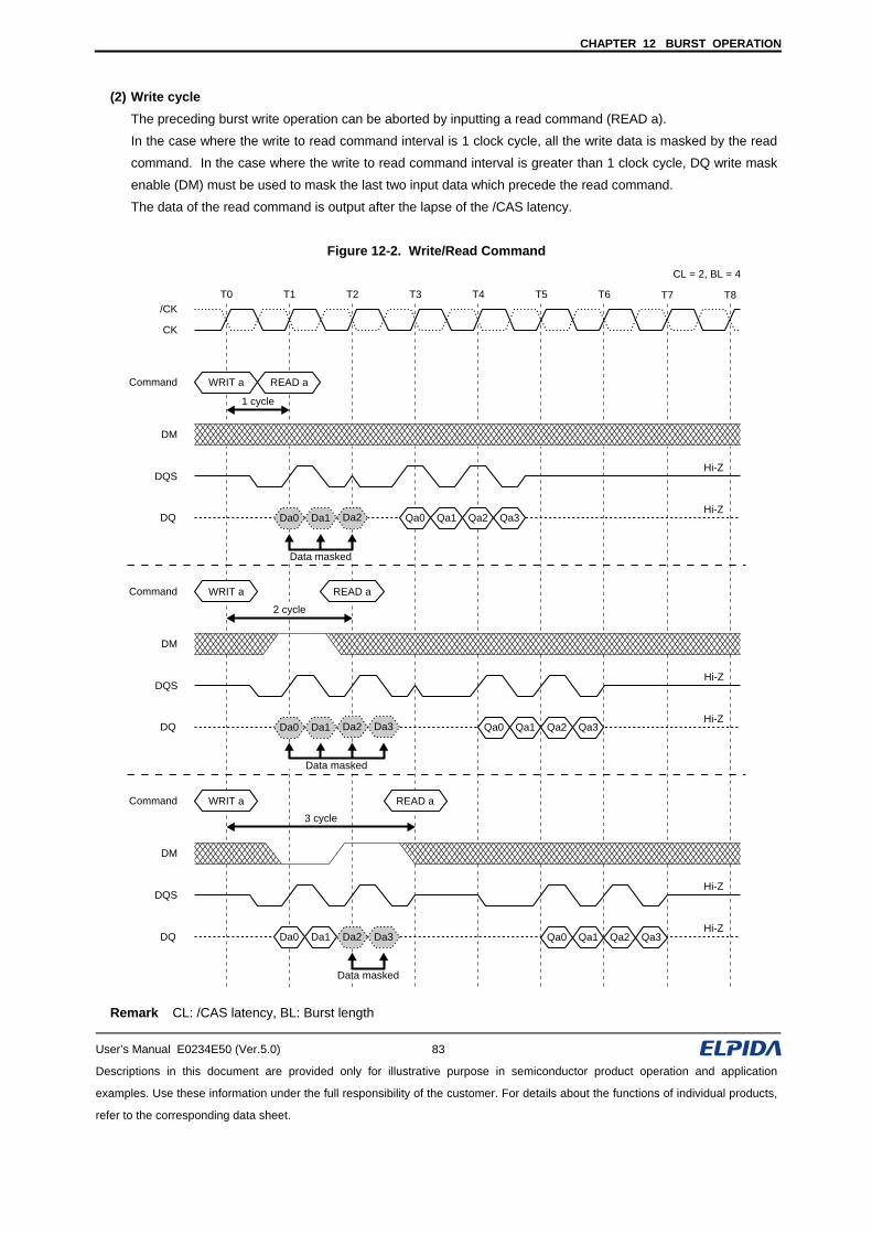
CHAPTER 12 BURST OPERATION
User’s Manual E0234E50 (Ver.5.0) 83
Descriptions in this document are provided only for illustrative purpose in semiconductor product operation and application
examples. Use these information under the full responsibility of the customer. For details about the functions of individual products,
refer to the corresponding data sheet.
(2) Write cycle The preceding burst write operation can be aborted by inputting a read command (READ a).
In the case where the write to read command interval is 1 clock cycle, all the write data is masked by the read
command. In the case where the write to read command interval is greater than 1 clock cycle, DQ write mask
enable (DM) must be used to mask the last two input data which precede the read command.
The data of the read command is output after the lapse of the /CAS latency.
Figure 12-2. Write/Read Command
/CK
Command
DQ
CK
T0 T1 T2 T3 T4 T5 T6 T7 T8
Da0 Da1 Da2 Qa0 Qa1 Qa2 Qa3Hi-Z
Hi-Z
CL = 2, BL = 4
DM
DQS
READ aWRIT a
Command
DQ Da0 Da1 Da2 Da3 Qa0 Qa1 Qa2 Qa3Hi-Z
Hi-Z
DM
DQS
READ aWRIT a
Command
DQ Da0 Da1 Da2 Da3 Qa0 Qa1 Qa2 Qa3Hi-Z
Hi-Z
DM
DQS
READ aWRIT a
1 cycle
3 cycle
Data masked
Data masked
2 cycle
Data masked
Remark CL: /CAS latency, BL: Burst length
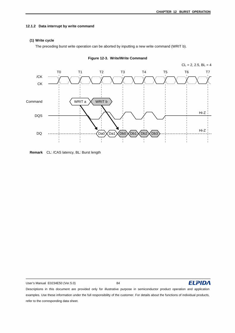
CHAPTER 12 BURST OPERATION
User’s Manual E0234E50 (Ver.5.0) 84
Descriptions in this document are provided only for illustrative purpose in semiconductor product operation and application
examples. Use these information under the full responsibility of the customer. For details about the functions of individual products,
refer to the corresponding data sheet.
12.1.2 Data interrupt by write command
(1) Write cycle
The preceding burst write operation can be aborted by inputting a new write command (WRIT b).
Figure 12-3. Write/Write Command
/CK
Command
DQ
CK
T0 T1 T2 T3 T4 T5 T6 T7
Da0 Da1 Db0 Db1 Db2 Db3Hi-Z
Hi-Z
CL = 2, 2.5, BL = 4
DQS
WRIT bWRIT a
Remark CL: /CAS latency, BL: Burst length
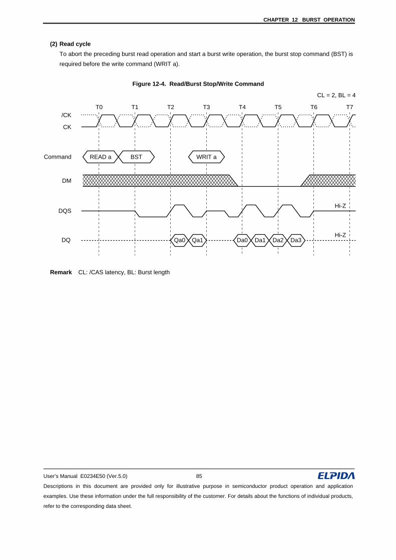
CHAPTER 12 BURST OPERATION
User’s Manual E0234E50 (Ver.5.0) 85
Descriptions in this document are provided only for illustrative purpose in semiconductor product operation and application
examples. Use these information under the full responsibility of the customer. For details about the functions of individual products,
refer to the corresponding data sheet.
(2) Read cycle To abort the preceding burst read operation and start a burst write operation, the burst stop command (BST) is
required before the write command (WRIT a).
Figure 12-4. Read/Burst Stop/Write Command
/CK
Command
DQ
CK
T0 T1 T2 T3 T4 T5 T6 T7
Qa0 Qa1 Da0 Da1 Da2 Da3Hi-Z
Hi-Z
CL = 2, BL = 4
DM
DQS
READ a BST WRIT a
Remark CL: /CAS latency, BL: Burst length
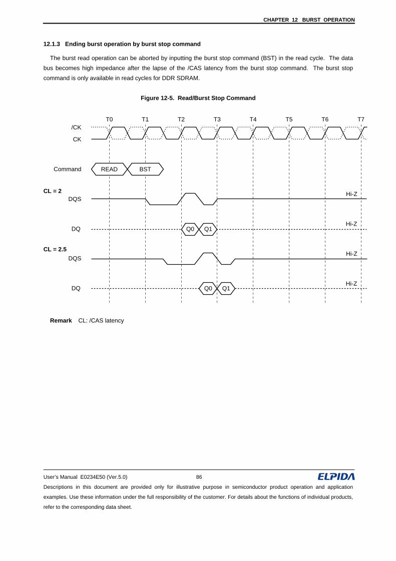
CHAPTER 12 BURST OPERATION
User’s Manual E0234E50 (Ver.5.0) 86
Descriptions in this document are provided only for illustrative purpose in semiconductor product operation and application
examples. Use these information under the full responsibility of the customer. For details about the functions of individual products,
refer to the corresponding data sheet.
12.1.3 Ending burst operation by burst stop command
The burst read operation can be aborted by inputting the burst stop command (BST) in the read cycle. The data
bus becomes high impedance after the lapse of the /CAS latency from the burst stop command. The burst stop
command is only available in read cycles for DDR SDRAM.
Figure 12-5. Read/Burst Stop Command
/CK
Command
DQ
CK
T0 T1 T2 T3 T4 T5 T6 T7
Q0 Q1Hi-Z
DQS
DQ Q0 Q1Hi-Z
Hi-Z
Hi-ZDQS
BSTREAD
CL = 2
CL = 2.5
Remark CL: /CAS latency
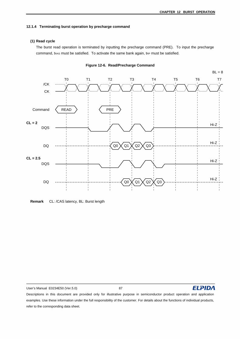
CHAPTER 12 BURST OPERATION
User’s Manual E0234E50 (Ver.5.0) 87
Descriptions in this document are provided only for illustrative purpose in semiconductor product operation and application
examples. Use these information under the full responsibility of the customer. For details about the functions of individual products,
refer to the corresponding data sheet.
12.1.4 Terminating burst operation by precharge command
(1) Read cycle
The burst read operation is terminated by inputting the precharge command (PRE). To input the precharge
command, tRAS must be satisfied. To activate the same bank again, tRP must be satisfied.
Figure 12-6. Read/Precharge Command
/CK
Command
DQ
CK
T0 T1 T2 T3 T4 T5 T6 T7
Q0 Q1 Q2 Q3Hi-Z
DQS
DQ Q0 Q1Hi-Z
Hi-Z
Hi-ZDQS
PREREAD
CL = 2
CL = 2.5
Q2 Q3
BL = 8
Remark CL: /CAS latency, BL: Burst length
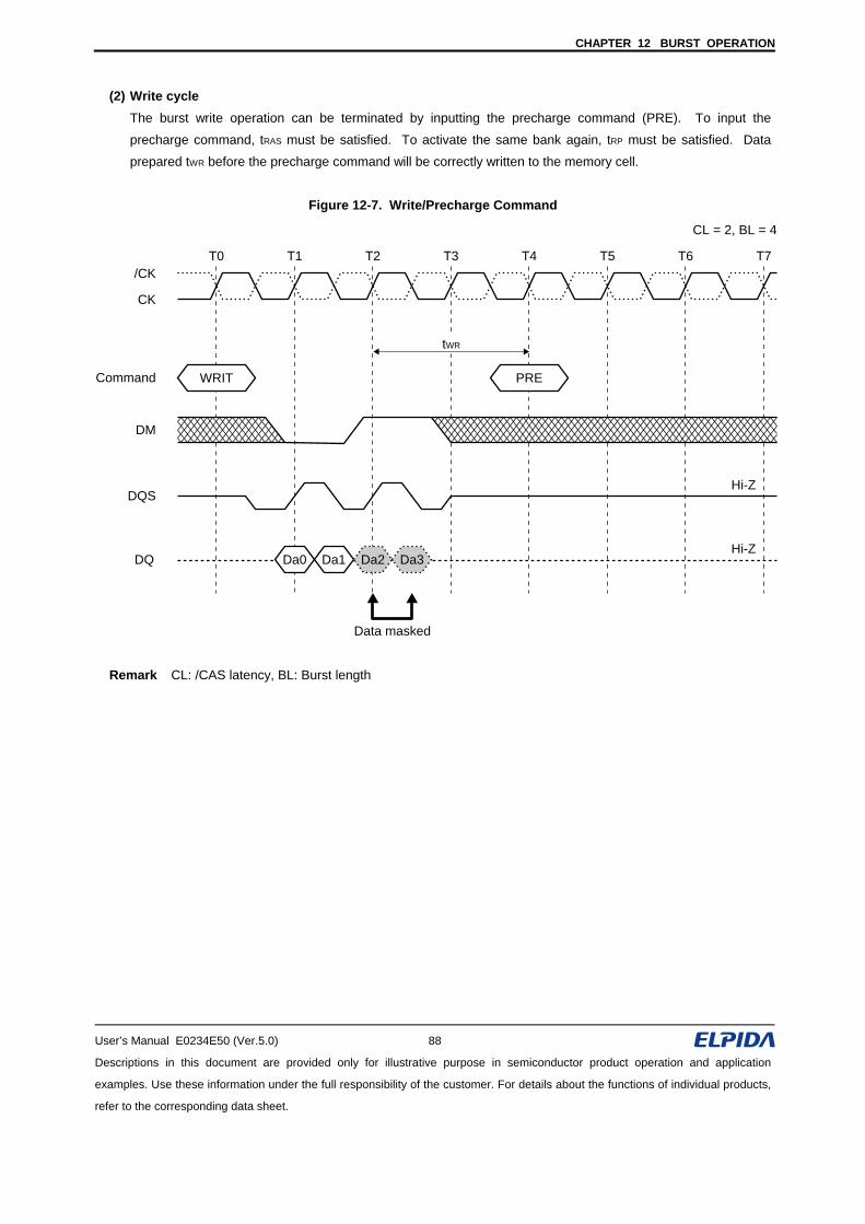
CHAPTER 12 BURST OPERATION
User’s Manual E0234E50 (Ver.5.0) 88
Descriptions in this document are provided only for illustrative purpose in semiconductor product operation and application
examples. Use these information under the full responsibility of the customer. For details about the functions of individual products,
refer to the corresponding data sheet.
(2) Write cycle The burst write operation can be terminated by inputting the precharge command (PRE). To input the
precharge command, tRAS must be satisfied. To activate the same bank again, tRP must be satisfied. Data
prepared tWR before the precharge command will be correctly written to the memory cell.
Figure 12-7. Write/Precharge Command
/CK
Command
DQ
CK
T0 T1 T2 T3 T4 T5 T6 T7
Da0 Da1 Da2 Da3Hi-Z
Hi-Z
CL = 2, BL = 4
DM
DQS
PREWRIT
Data masked
tWR
Remark CL: /CAS latency, BL: Burst length
The information in this document is current as July, 2007. The information is subject to change without notice.
NOTES FOR CMOS DEVICES
1 PRECAUTION AGAINST ESD FOR MOS DEVICES
Exposing the MOS devices to a strong electric field can cause destruction of the gate oxide and ultimately degrade the MOS devices operation. Steps must be taken to stop generation of static electricity as much as possible, and quickly dissipate it, when once it has occurred. Environmental control must be adequate. When it is dry, humidifier should be used. It is recommended to avoid using insulators that easily build static electricity. MOS devices must be stored and transported in an anti-static container, static shielding bag or conductive material. All test and measurement tools including work bench and floor should be grounded. The operator should be grounded using wrist strap. MOS devices must not be touched with bare hands. Similar precautions need to be taken for PW boards with semiconductor MOS devices on it.
2 HANDLING OF UNUSED INPUT PINS FOR CMOS DEVICES
No connection for CMOS devices input pins can be a cause of malfunction. If no connection is provided to the input pins, it is possible that an internal input level may be generated due to noise, etc., hence causing malfunction. CMOS devices behave differently than Bipolar or NMOS devices. Input levels of CMOS devices must be fixed high or low by using a pull-up or pull-down circuitry. Each unused pin should be connected to VDD or GND with a resistor, if it is considered to have a possibility of being an output pin. The unused pins must be handled in accordance with the related specifications.
3 STATUS BEFORE INITIALIZATION OF MOS DEVICES
Power-on does not necessarily define initial status of MOS devices. Production process of MOS does not define the initial operation status of the device. Immediately after the power source is turned ON, the MOS devices with reset function have not yet been initialized. Hence, power-on does not guarantee output pin levels, I/O settings or contents of registers. MOS devices are not initialized until the reset signal is received. Reset operation must be executed immediately after power-on for MOS devices having reset function.
CME0107
M01E0706
No part of this document may be copied or reproduced in any form or by any means without the prior written consent of Elpida Memory, Inc.
Elpida Memory, Inc. does not assume any liability for infringement of any intellectual property rights (including but not limited to patents, copyrights, and circuit layout licenses) of Elpida Memory, Inc. or third parties by or arising from the use of the products or information listed in this document. No license, express, implied or otherwise, is granted under any patents, copyrights or other intellectual property rights of Elpida Memory, Inc. or others.
Descriptions of circuits, software and other related information in this document are provided for illustrative purposes in semiconductor product operation and application examples. The incorporation of these circuits, software and information in the design of the customer's equipment shall be done under the full responsibility of the customer. Elpida Memory, Inc. assumes no responsibility for any losses incurred by customers or third parties arising from the use of these circuits, software and information.
[Product applications]Be aware that this product is for use in typical electronic equipment for general-purpose applications.Elpida Memory, Inc. makes every attempt to ensure that its products are of high quality and reliability. However, users are instructed to contact Elpida Memory's sales office before using the product in aerospace, aeronautics, nuclear power, combustion control, transportation, traffic, safety equipment, medical equipment for life support, or other such application in which especially high quality and reliability is demanded or where its failure or malfunction may directly threaten human life or cause risk of bodily injury.
[Product usage]Design your application so that the product is used within the ranges and conditions guaranteed by Elpida Memory, Inc., including the maximum ratings, operating supply voltage range, heat radiation characteristics, installation conditions and other related characteristics. Elpida Memory, Inc. bears no responsibility for failure or damage when the product is used beyond the guaranteed ranges and conditions. Even within the guaranteed ranges and conditions, consider normally foreseeable failure rates or failure modes in semiconductor devices and employ systemic measures such as fail-safes, so that the equipment incorporating Elpida Memory, Inc. products does not cause bodily injury, fire or other consequential damage due to the operation of the Elpida Memory, Inc. product.
[Usage environment]
Usage in environments with special characteristics as listed below was not considered in the design. Accordingly, our company assumes no responsibility for loss of a customer or a third party when used in environments with the special characteristics listed below.
Example:1) Usage in liquids, including water, oils, chemicals and organic solvents.2) Usage in exposure to direct sunlight or the outdoors, or in dusty places. 3) Usage involving exposure to significant amounts of corrosive gas, including sea air, CL2, H2S, NH3,
SO2, and NOx.4) Usage in environments with static electricity, or strong electromagnetic waves or radiation. 5) Usage in places where dew forms. 6) Usage in environments with mechanical vibration, impact, or stress. 7) Usage near heating elements, igniters, or flammable items.
If you export the products or technology described in this document that are controlled by the Foreign Exchange and Foreign Trade Law of Japan, you must follow the necessary procedures in accordance with the relevant laws and regulations of Japan. Also, if you export products/technology controlled by U.S. export control regulations, or another country's export control laws or regulations, you must follow the necessary procedures in accordance with such laws or regulations.If these products/technology are sold, leased, or transferred to a third party, or a third party is granted
license to use these products, that third party must be made aware that they are responsible for compliance with the relevant laws and regulations.
The information in this document is subject to change without notice. Before using this document, confirm that this is the latest version.