Embed Size (px)
Citation preview
Summary This document describes a reference design for interfacing CoolRunner™-II CPLDs with double data rate (DDR) SDRAM memory devices. The built reference design is capable of 100 MHz operation. The VHDL code described here can be found in VHDL Code, page 19.
Introduction CoolRunner-II CPLDs are the latest CPLD product offering from Xilinx. CoolRunner-II CPLDs combine high performance with low power operation. More information on the CoolRunner-II CPLD family can be found at http://www.xilinx.com/cr2.
Key features of the CoolRunner-II CPLD family include DualEDGE triggered registers, a global clock divider, and voltage referenced I/O standards including SSTL_2. These features provide the capability to interface a CoolRunner-II CPLD with high speed memory devices such as DDR SDRAM. This document provides background information on DDR SDRAM devices and discusses the CPLD design capable of this interface.
Signal Definitions
Table 1 defines the DDR SDRAM interface signals described in this document. Signal names are commonly used from both DDR SDRAM manufacturers as well as the described CPLD VHDL code.
Application Note: CoolRunner-II CPLDs
XAPP384 (v1.0) Febuary 14, 2003
Interfacing to DDR SDRAM with CoolRunner-II CPLDs
R
Table 1: DDR SDRAM Signal Definitions
Manufacturer Specification
Xilinx CPLD VHDL Code Description
CK ddr_clk Differential clock pair. All address and control signals sampled at crossing point of CK and CK#.CK# ddr_clkn
CKE ddr_cke Clock enable.
CS# ddr_cs
Command signals that define current operation.RAS# ddr_ras
CAS# ddr_cas
WE# ddr_we
DM ddr_dm Mask signal for write data operations.
BA[1:0] ddr_ba[1:0] 2-bit bank address bus.
A[11:0] ddr_a[11:0] 12-bit row and column address bus.
DQ[7:0] ddr_dq[7:0] Bidirectional 8-bit data bus.
DQS ddr_dqs Bidirectional data strobe.
XAPP384 (v1.0) Febuary 14, 2003 www.xilinx.com 11-800-255-7778
© 2003 Xilinx, Inc. All rights reserved. All Xilinx trademarks, registered trademarks, patents, and further disclaimers are as listed at http://www.xilinx.com/legal.htm. All other trademarks and registered trademarks are the property of their respective owners. All specifications are subject to change without notice.
NOTICE OF DISCLAIMER: Xilinx is providing this design, code, or information "as is." By providing the design, code, or information as one possible implementation of this fea-ture, application, or standard, Xilinx makes no representation that this implementation is free from any claims of infringement. You are responsible for obtaining any rights you may require for your implementation. Xilinx expressly disclaims any warranty whatsoever with respect to the adequacy of the implementation, including but not limited to any warran-ties or representations that this implementation is free from claims of infringement and any implied warranties of merchantability or fitness for a particular purpose.
Interfacing to DDR SDRAM with CoolRunner-II CPLDsR
DDR SDRAM DDR SDRAM memory devices provide a migration path from single data rate (SDR) memory devices for enhanced applications. DDR memory doubles the bandwidth of the device without increasing the clock speed or bus width. DDR SDRAM provides a source-synchronous data capture at a rate of twice the clock frequency. These devices utilize a 2n-prefetch architecture where the internal data bus is twice the size of the external data bus.
The core of a DDR SDRAM is similar to SDR SDRAM with identical address and control interfaces, bank structures and refresh requirements. The main difference between DDR and SDR SDRAM is in the actual data interface. SDR is fully synchronous using the positive edge of the clock. DDR is true source-synchronous and captures data twice per clock cycle with a bidirectional data strobe, DQS.
Data strobe signals were added to DDR devices to achieve higher data rates. Data strobes are non-free running signals that are controlled by the device which is driving data signals (e.g., DDR SDRAM or the CPLD). During write operations to the DDR, the controller drives the data strobe, DQS. During read operations, the DDR SDRAM drives DQS.
The following list is a summary of enhancements for DDR devices:
• DDR utilizes a differential pair for the system clock (CK and CK#)
• Data is transmitted on both positive and negative edges of the clock
• DDR devices incorporate an on-chip delay locked loop (DLL)
• Data strobes are added to improve data capture reliability
• SSTL-2 signaling techniques are used
Xilinx Board Design
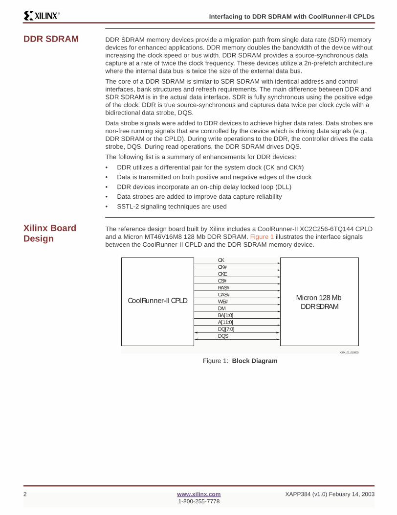
The reference design board built by Xilinx includes a CoolRunner-II XC2C256-6TQ144 CPLD and a Micron MT46V16M8 128 Mb DDR SDRAM. Figure 1 illustrates the interface signals between the CoolRunner-II CPLD and the DDR SDRAM memory device.
Figure 1: Block Diagram
CoolRunner-II CPLD Micron 128 Mb DDR SDRAM
CKCK#CKECS#RAS#CAS#WE#DMBA[1:0]A[11:0]DQ[7:0]DQS
X384_01_010803
2 www.xilinx.com XAPP384 (v1.0) Febuary 14, 20031-800-255-7778
Interfacing to DDR SDRAM with CoolRunner-II CPLDsR
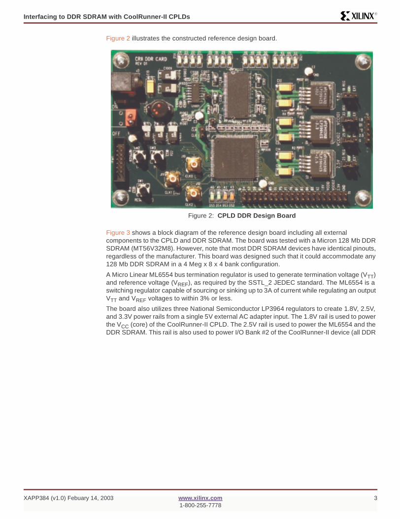
Figure 2 illustrates the constructed reference design board.
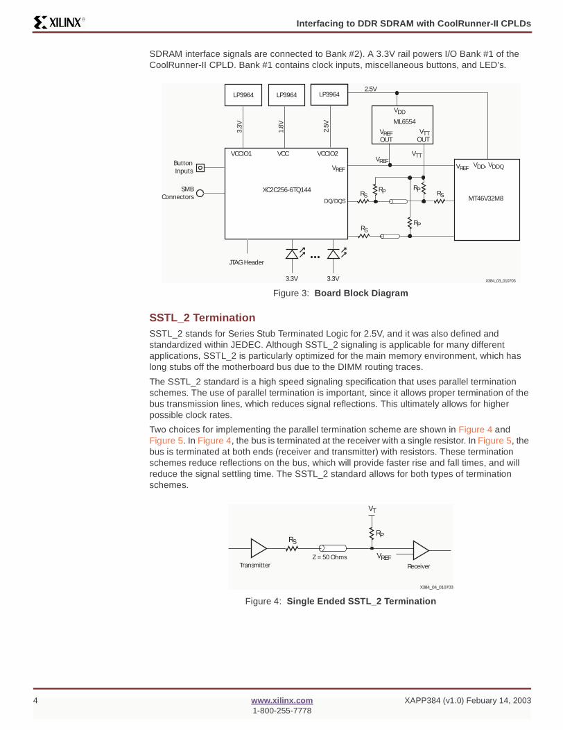
Figure 3 shows a block diagram of the reference design board including all external components to the CPLD and DDR SDRAM. The board was tested with a Micron 128 Mb DDR SDRAM (MT56V32M8). However, note that most DDR SDRAM devices have identical pinouts, regardless of the manufacturer. This board was designed such that it could accommodate any 128 Mb DDR SDRAM in a 4 Meg x 8 x 4 bank configuration.
A Micro Linear ML6554 bus termination regulator is used to generate termination voltage (VTT) and reference voltage (VREF), as required by the SSTL_2 JEDEC standard. The ML6554 is a switching regulator capable of sourcing or sinking up to 3A of current while regulating an output VTT and VREF voltages to within 3% or less.
The board also utilizes three National Semiconductor LP3964 regulators to create 1.8V, 2.5V, and 3.3V power rails from a single 5V external AC adapter input. The 1.8V rail is used to power the VCC (core) of the CoolRunner-II CPLD. The 2.5V rail is used to power the ML6554 and the DDR SDRAM. This rail is also used to power I/O Bank #2 of the CoolRunner-II device (all DDR
Figure 2: CPLD DDR Design Board
XAPP384 (v1.0) Febuary 14, 2003 www.xilinx.com 31-800-255-7778
Interfacing to DDR SDRAM with CoolRunner-II CPLDsR
SDRAM interface signals are connected to Bank #2). A 3.3V rail powers I/O Bank #1 of the CoolRunner-II CPLD. Bank #1 contains clock inputs, miscellaneous buttons, and LED's.
SSTL_2 TerminationSSTL_2 stands for Series Stub Terminated Logic for 2.5V, and it was also defined and standardized within JEDEC. Although SSTL_2 signaling is applicable for many different applications, SSTL_2 is particularly optimized for the main memory environment, which has long stubs off the motherboard bus due to the DIMM routing traces.
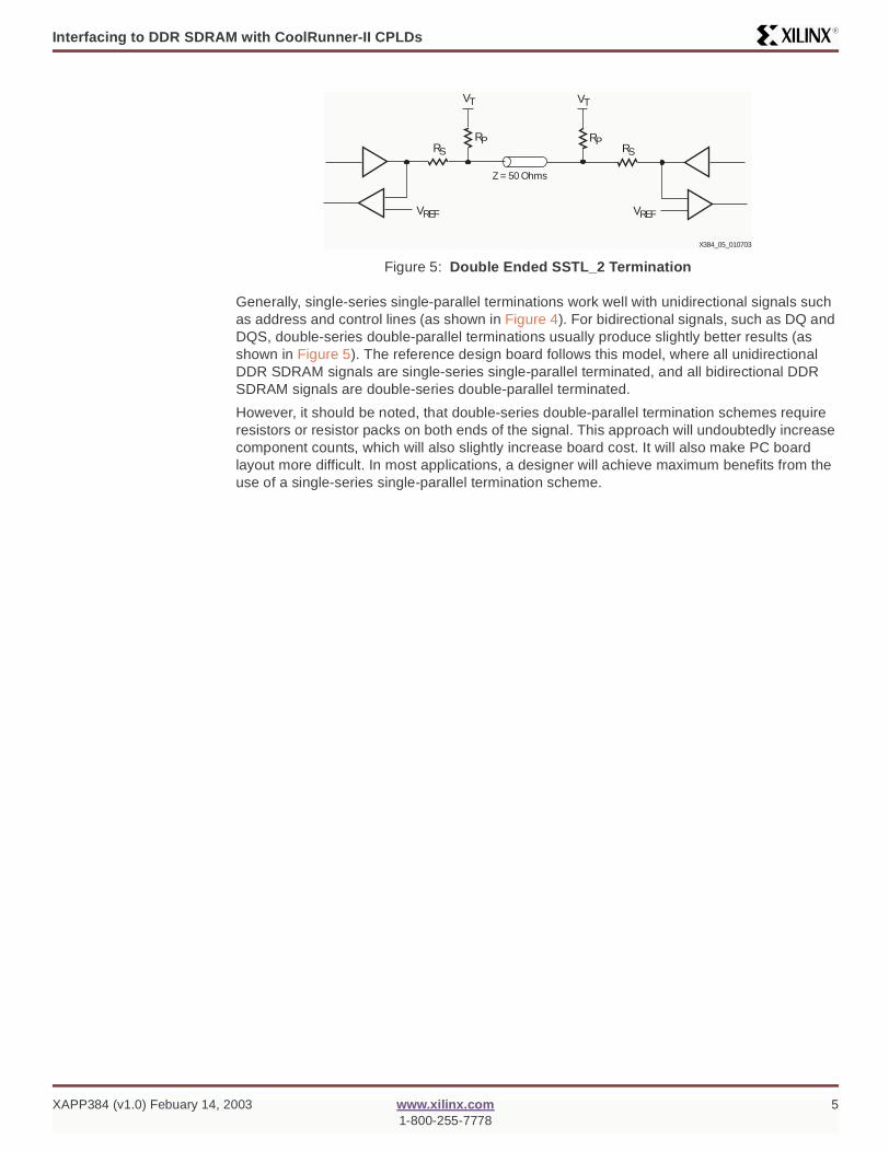
The SSTL_2 standard is a high speed signaling specification that uses parallel termination schemes. The use of parallel termination is important, since it allows proper termination of the bus transmission lines, which reduces signal reflections. This ultimately allows for higher possible clock rates.
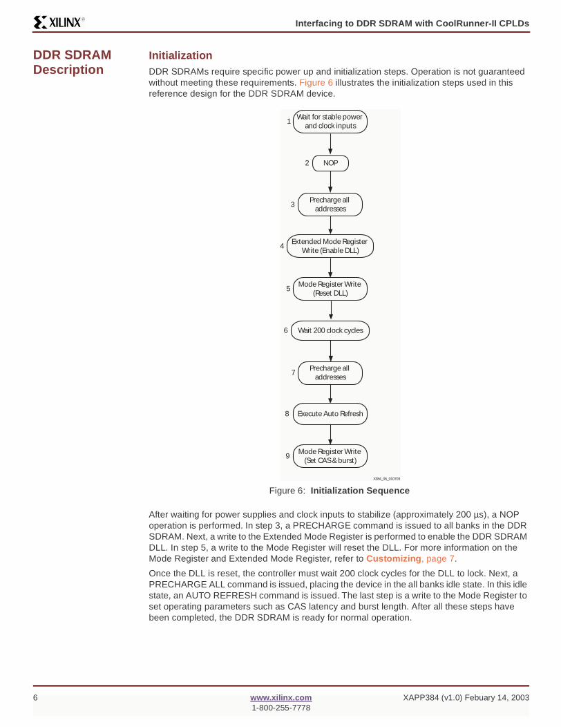
Two choices for implementing the parallel termination scheme are shown in Figure 4 and Figure 5. In Figure 4, the bus is terminated at the receiver with a single resistor. In Figure 5, the bus is terminated at both ends (receiver and transmitter) with resistors. These termination schemes reduce reflections on the bus, which will provide faster rise and fall times, and will reduce the signal settling time. The SSTL_2 standard allows for both types of termination schemes.
Figure 3: Board Block Diagram
Figure 4: Single Ended SSTL_2 Termination
SMB Connectors
LP3964 LP3964LP3964LP3964LP3964
3.3V
1.8V
VCCVCCIO1
2.5V
VCCIO2
XC2C256-6TQ144MT46V32M8
ML6554
2.5V
VREFVTT
Button Inputs
JTAG Header
3.3V 3.3V
VREF
RSRP
RSRP
RSRP
DQ/DQS
X384_03_010703
VDD
VREF OUT
VTT OUT
VDD, VDDQVREF
VREF
RSRP
Transmitter Receiver
VT
Z = 50 Ohms
X384_04_010703
4 www.xilinx.com XAPP384 (v1.0) Febuary 14, 20031-800-255-7778
Interfacing to DDR SDRAM with CoolRunner-II CPLDsR
Generally, single-series single-parallel terminations work well with unidirectional signals such as address and control lines (as shown in Figure 4). For bidirectional signals, such as DQ and DQS, double-series double-parallel terminations usually produce slightly better results (as shown in Figure 5). The reference design board follows this model, where all unidirectional DDR SDRAM signals are single-series single-parallel terminated, and all bidirectional DDR SDRAM signals are double-series double-parallel terminated.
However, it should be noted, that double-series double-parallel termination schemes require resistors or resistor packs on both ends of the signal. This approach will undoubtedly increase component counts, which will also slightly increase board cost. It will also make PC board layout more difficult. In most applications, a designer will achieve maximum benefits from the use of a single-series single-parallel termination scheme.
Figure 5: Double Ended SSTL_2 Termination
VREF
RSRP
VT
Z = 50 Ohms
VREF
RP
VT
RS
X384_05_010703
XAPP384 (v1.0) Febuary 14, 2003 www.xilinx.com 51-800-255-7778
Interfacing to DDR SDRAM with CoolRunner-II CPLDsR
DDR SDRAM Description
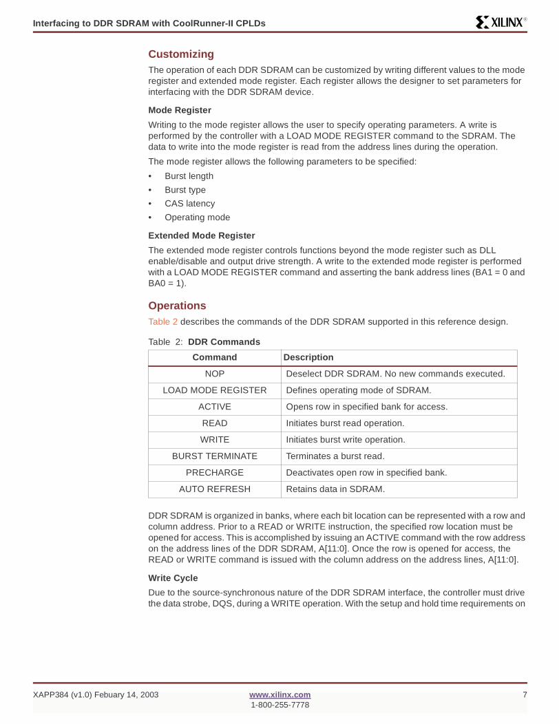
InitializationDDR SDRAMs require specific power up and initialization steps. Operation is not guaranteed without meeting these requirements. Figure 6 illustrates the initialization steps used in this reference design for the DDR SDRAM device.
After waiting for power supplies and clock inputs to stabilize (approximately 200 µs), a NOP operation is performed. In step 3, a PRECHARGE command is issued to all banks in the DDR SDRAM. Next, a write to the Extended Mode Register is performed to enable the DDR SDRAM DLL. In step 5, a write to the Mode Register will reset the DLL. For more information on the Mode Register and Extended Mode Register, refer to Customizing, page 7.
Once the DLL is reset, the controller must wait 200 clock cycles for the DLL to lock. Next, a PRECHARGE ALL command is issued, placing the device in the all banks idle state. In this idle state, an AUTO REFRESH command is issued. The last step is a write to the Mode Register to set operating parameters such as CAS latency and burst length. After all these steps have been completed, the DDR SDRAM is ready for normal operation.
Figure 6: Initialization Sequence
X384_06_010703
Wait for stable power and clock inputs
NOP
Precharge all addresses
Extended Mode Register Write (Enable DLL)
Mode Register Write (Reset DLL)
Wait 200 clock cycles
Precharge all addresses
Mode Register Write (Set CAS & burst)
Execute Auto Refresh
1
2
3
4
5
6
7
8
9
6 www.xilinx.com XAPP384 (v1.0) Febuary 14, 20031-800-255-7778
Interfacing to DDR SDRAM with CoolRunner-II CPLDsR
CustomizingThe operation of each DDR SDRAM can be customized by writing different values to the mode register and extended mode register. Each register allows the designer to set parameters for interfacing with the DDR SDRAM device.
Mode Register
Writing to the mode register allows the user to specify operating parameters. A write is performed by the controller with a LOAD MODE REGISTER command to the SDRAM. The data to write into the mode register is read from the address lines during the operation.
The mode register allows the following parameters to be specified:
• Burst length
• Burst type
• CAS latency
• Operating mode
Extended Mode Register
The extended mode register controls functions beyond the mode register such as DLL enable/disable and output drive strength. A write to the extended mode register is performed with a LOAD MODE REGISTER command and asserting the bank address lines (BA1 = 0 and BA0 = 1).
OperationsTable 2 describes the commands of the DDR SDRAM supported in this reference design.
DDR SDRAM is organized in banks, where each bit location can be represented with a row and column address. Prior to a READ or WRITE instruction, the specified row location must be opened for access. This is accomplished by issuing an ACTIVE command with the row address on the address lines of the DDR SDRAM, A[11:0]. Once the row is opened for access, the READ or WRITE command is issued with the column address on the address lines, A[11:0].
Write Cycle
Due to the source-synchronous nature of the DDR SDRAM interface, the controller must drive the data strobe, DQS, during a WRITE operation. With the setup and hold time requirements on
Table 2: DDR Commands
Command Description
NOP Deselect DDR SDRAM. No new commands executed.
LOAD MODE REGISTER Defines operating mode of SDRAM.
ACTIVE Opens row in specified bank for access.
READ Initiates burst read operation.
WRITE Initiates burst write operation.
BURST TERMINATE Terminates a burst read.
PRECHARGE Deactivates open row in specified bank.
AUTO REFRESH Retains data in SDRAM.
XAPP384 (v1.0) Febuary 14, 2003 www.xilinx.com 71-800-255-7778
Interfacing to DDR SDRAM with CoolRunner-II CPLDsR
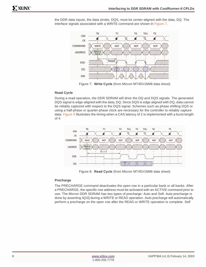
the DDR data inputs, the data strobe, DQS, must be center-aligned with the data, DQ. The interface signals associated with a WRITE command are shown in Figure 7.
Read Cycle
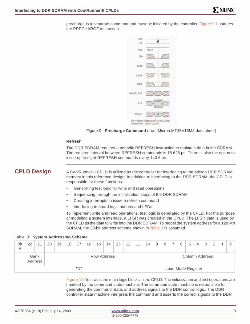
During a read operation, the DDR SDRAM will drive the DQ and DQS signals. The generated DQS signal is edge-aligned with the data, DQ. Since DQS is edge aligned with DQ, data cannot be reliably captured with respect to the DQS signal. Schemes such as phase shifting DQS or using a half-phase or quarter-phase clock are necessary for the controller to reliably capture data. Figure 8 illustrates the timing when a CAS latency of 2 is implemented with a burst length of 4.
Precharge
The PRECHARGE command deactivates the open row in a particular bank or all banks. After a PRECHARGE, the specific row address must be activated with an ACTIVE command prior to use. The Micron DDR SDRAM has two types of precharge: Auto and Self. Auto precharge is done by asserting A[10] during a WRITE or READ operation. Auto precharge will automatically perform a precharge on the open row after the READ or WRITE operation is complete. Self
Figure 7: Write Cycle (from Micron MT45V16M8 data sheet)
Figure 8: Read Cycle (from Micron MT45V16M8 data sheet)
8 www.xilinx.com XAPP384 (v1.0) Febuary 14, 20031-800-255-7778
Interfacing to DDR SDRAM with CoolRunner-II CPLDsR
precharge is a separate command and must be initiated by the controller. Figure 9 illustrates the PRECHARGE instruction.
Refresh
The DDR SDRAM requires a periodic REFRESH instruction to maintain data in the SDRAM. The required interval between REFRESH commands is 15.625 µs. There is also the option to issue up to eight REFRESH commands every 140.6 µs.
CPLD Design A CoolRunner-II CPLD is utilized as the controller for interfacing to the Micron DDR SDRAM memory in this reference design. In addition to interfacing to the DDR SDRAM, the CPLD is responsible for these functions:
• Generating test logic for write and read operations
• Sequencing through the initialization steps of the DDR SDRAM
• Creating interrupts to issue a refresh command
• Interfacing to board logic buttons and LEDs
To implement write and read operations, test logic is generated by the CPLD. For the purpose of modeling a system interface, a LFSR was created in the CPLD. The LFSR data is used by the CPLD as the data to write into the DDR SDRAM. To model the system address for a 128 Mb SDRAM, the 23-bit address scheme shown in Table 3 is assumed.
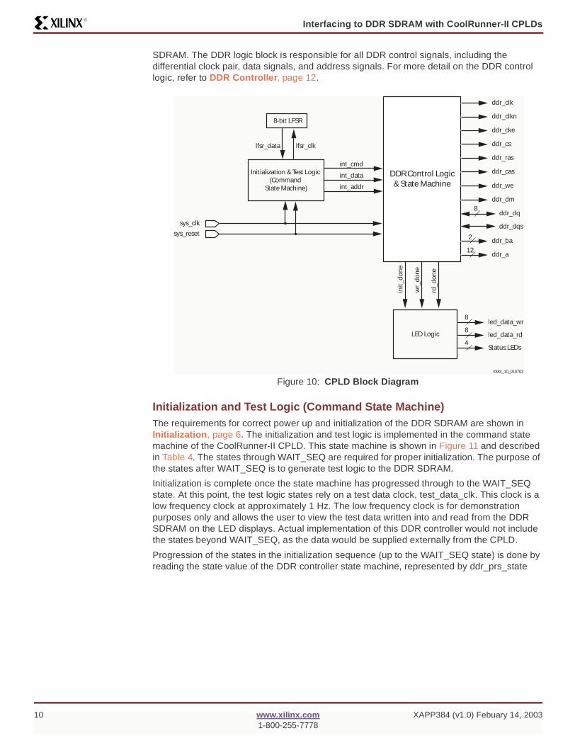
Figure 10 illustrates the main logic blocks in the CPLD. The initialization and test operations are handled by the command state machine. The command state machine is responsible for generating the command, data, and address signals to the DDR control logic. The DDR controller state machine interprets the command and asserts the correct signals to the DDR
Figure 9: Precharge Command (from Micron MT45V16M8 data sheet)
Table 3: System Addressing Scheme
Bit#
22 21 20 19 18 17 16 15 14 13 12 11 10 9 8 7 6 5 4 3 2 1 0
Bank Address
Row Address Column Address
"X" Load Mode Register
XAPP384 (v1.0) Febuary 14, 2003 www.xilinx.com 91-800-255-7778
Interfacing to DDR SDRAM with CoolRunner-II CPLDsR
SDRAM. The DDR logic block is responsible for all DDR control signals, including the differential clock pair, data signals, and address signals. For more detail on the DDR control logic, refer to DDR Controller, page 12.
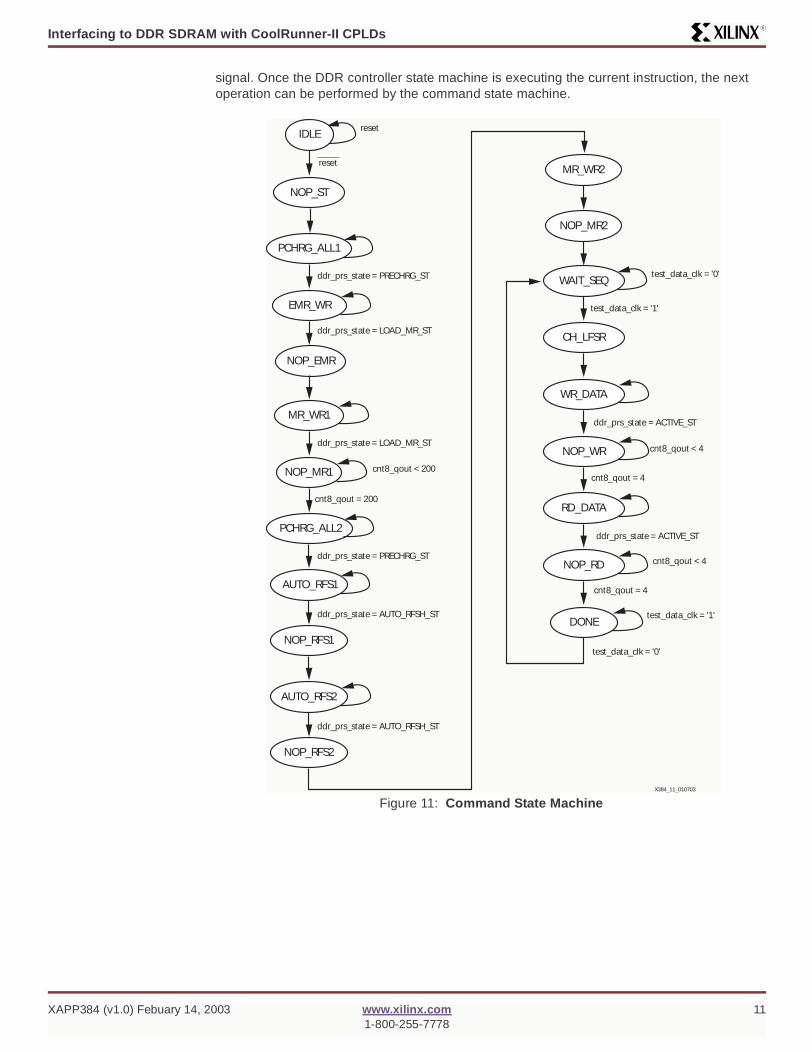
Initialization and Test Logic (Command State Machine)The requirements for correct power up and initialization of the DDR SDRAM are shown in Initialization, page 6. The initialization and test logic is implemented in the command state machine of the CoolRunner-II CPLD. This state machine is shown in Figure 11 and described in Table 4. The states through WAIT_SEQ are required for proper initialization. The purpose of the states after WAIT_SEQ is to generate test logic to the DDR SDRAM.
Initialization is complete once the state machine has progressed through to the WAIT_SEQ state. At this point, the test logic states rely on a test data clock, test_data_clk. This clock is a low frequency clock at approximately 1 Hz. The low frequency clock is for demonstration purposes only and allows the user to view the test data written into and read from the DDR SDRAM on the LED displays. Actual implementation of this DDR controller would not include the states beyond WAIT_SEQ, as the data would be supplied externally from the CPLD.
Progression of the states in the initialization sequence (up to the WAIT_SEQ state) is done by reading the state value of the DDR controller state machine, represented by ddr_prs_state
Figure 10: CPLD Block Diagram
ddr_clk
ddr_clkn
ddr_cke
ddr_cs
ddr_ras
ddr_cas
ddr_we
ddr_dm
ddr_dq
ddr_dqs
ddr_ba
ddr_a
8
12
2
DDR Control Logic & State Machine
int_cmd
int_data
int_addr
Initialization & Test Logic (Command
State Machine)
8-bit LFSR
lfsr_clklfsr_data
sys_clk
sys_reset
LED Logic
led_data_wr8
led_data_rd8
Status LEDs4
init
_do
ne
wr_
do
ne
rd_d
on
e
X384_10_010703
10 www.xilinx.com XAPP384 (v1.0) Febuary 14, 20031-800-255-7778
Interfacing to DDR SDRAM with CoolRunner-II CPLDsR
signal. Once the DDR controller state machine is executing the current instruction, the next operation can be performed by the command state machine.
Figure 11: Command State MachineX384_11_010703
EMR_WR
NOP_EMR
MR_WR1
NOP_MR1
PCHRG_ALL1
ddr_prs_state = PRECHRG_ST
reset
reset
IDLE
NOP_ST
ddr_prs_state = LOAD_MR_ST
ddr_prs_state = LOAD_MR_ST
PCHRG_ALL2
AUTO_RFS1
cnt8_qout < 200
cnt8_qout = 200
ddr_prs_state = PRECHRG_ST
ddr_prs_state = AUTO_RFSH_ST
NOP_RFS1
AUTO_RFS2
ddr_prs_state = AUTO_RFSH_ST
NOP_RFS2
MR_WR2
NOP_MR2
WAIT_SEQ
CH_LFSR
test_data_clk = '0'
test_data_clk = '1'
WR_DATA
ddr_prs_state = ACTIVE_ST
NOP_WR
RD_DATA
ddr_prs_state = ACTIVE_ST
NOP_RD
DONE
cnt8_qout < 4
cnt8_qout = 4
cnt8_qout < 4
cnt8_qout = 4
test_data_clk = '0'
test_data_clk = '1'
XAPP384 (v1.0) Febuary 14, 2003 www.xilinx.com 111-800-255-7778
Interfacing to DDR SDRAM with CoolRunner-II CPLDsR
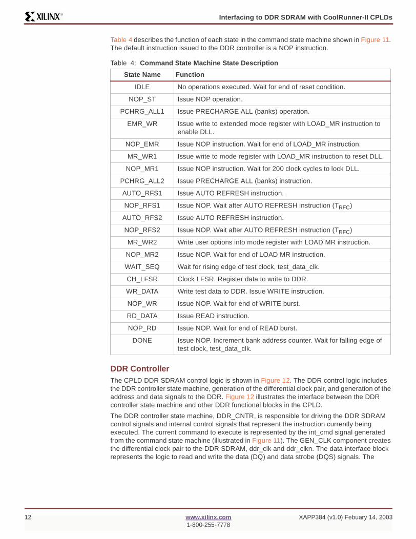
Table 4 describes the function of each state in the command state machine shown in Figure 11. The default instruction issued to the DDR controller is a NOP instruction.
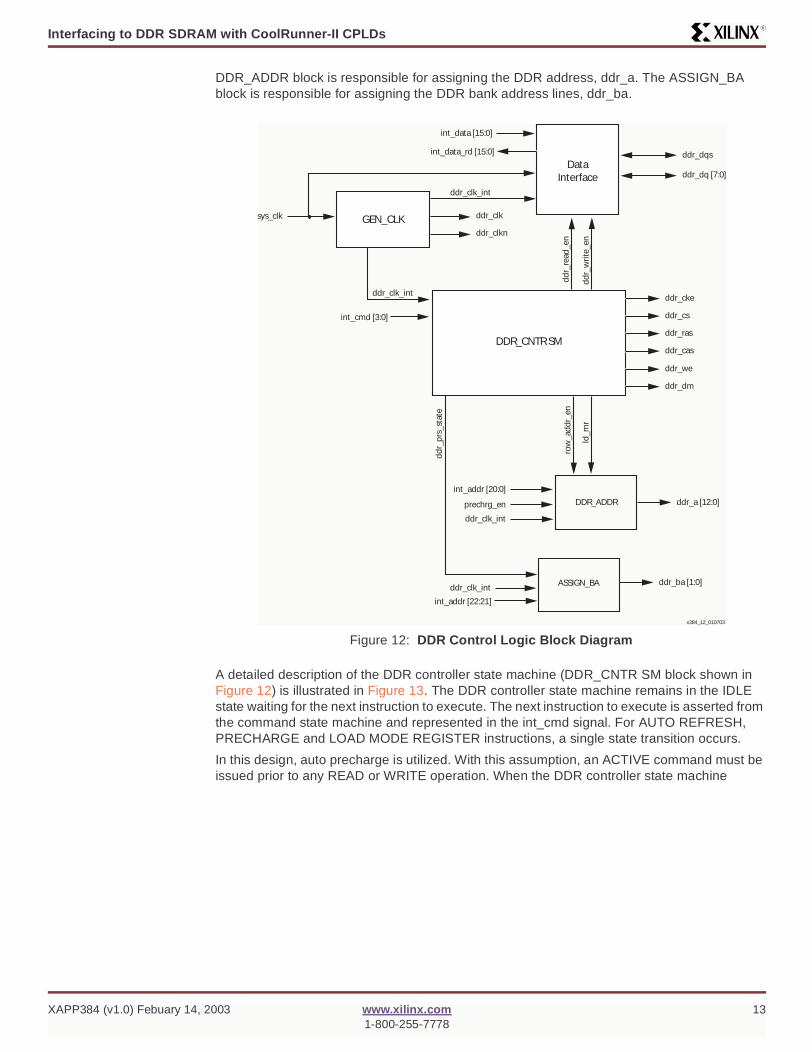
DDR ControllerThe CPLD DDR SDRAM control logic is shown in Figure 12. The DDR control logic includes the DDR controller state machine, generation of the differential clock pair, and generation of the address and data signals to the DDR. Figure 12 illustrates the interface between the DDR controller state machine and other DDR functional blocks in the CPLD.
The DDR controller state machine, DDR_CNTR, is responsible for driving the DDR SDRAM control signals and internal control signals that represent the instruction currently being executed. The current command to execute is represented by the int_cmd signal generated from the command state machine (illustrated in Figure 11). The GEN_CLK component creates the differential clock pair to the DDR SDRAM, ddr_clk and ddr_clkn. The data interface block represents the logic to read and write the data (DQ) and data strobe (DQS) signals. The
Table 4: Command State Machine State Description
State Name Function
IDLE No operations executed. Wait for end of reset condition.
NOP_ST Issue NOP operation.
PCHRG_ALL1 Issue PRECHARGE ALL (banks) operation.
EMR_WR Issue write to extended mode register with LOAD_MR instruction to enable DLL.
NOP_EMR Issue NOP instruction. Wait for end of LOAD_MR instruction.
MR_WR1 Issue write to mode register with LOAD_MR instruction to reset DLL.
NOP_MR1 Issue NOP instruction. Wait for 200 clock cycles to lock DLL.
PCHRG_ALL2 Issue PRECHARGE ALL (banks) instruction.
AUTO_RFS1 Issue AUTO REFRESH instruction.
NOP_RFS1 Issue NOP. Wait after AUTO REFRESH instruction (TRFC)
AUTO_RFS2 Issue AUTO REFRESH instruction.
NOP_RFS2 Issue NOP. Wait after AUTO REFRESH instruction (TRFC)
MR_WR2 Write user options into mode register with LOAD MR instruction.
NOP_MR2 Issue NOP. Wait for end of LOAD MR instruction.
WAIT_SEQ Wait for rising edge of test clock, test_data_clk.
CH_LFSR Clock LFSR. Register data to write to DDR.
WR_DATA Write test data to DDR. Issue WRITE instruction.
NOP_WR Issue NOP. Wait for end of WRITE burst.
RD_DATA Issue READ instruction.
NOP_RD Issue NOP. Wait for end of READ burst.
DONE Issue NOP. Increment bank address counter. Wait for falling edge of test clock, test_data_clk.
12 www.xilinx.com XAPP384 (v1.0) Febuary 14, 20031-800-255-7778
Interfacing to DDR SDRAM with CoolRunner-II CPLDsR
DDR_ADDR block is responsible for assigning the DDR address, ddr_a. The ASSIGN_BA block is responsible for assigning the DDR bank address lines, ddr_ba.
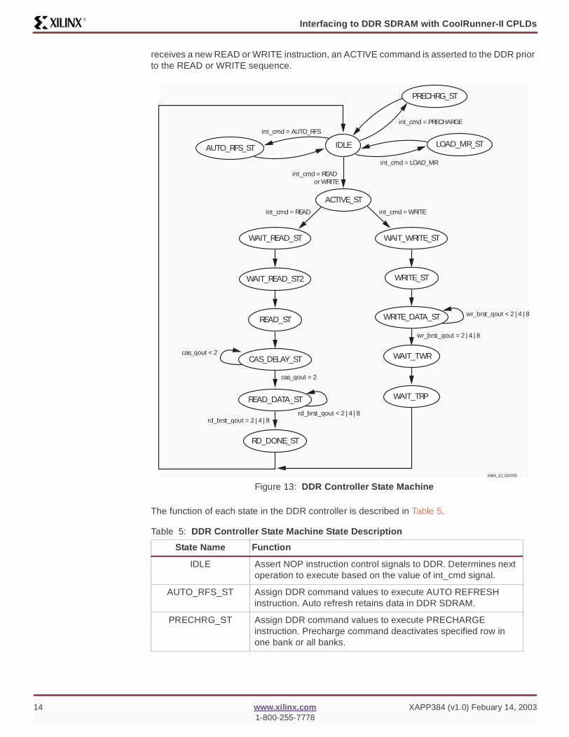
A detailed description of the DDR controller state machine (DDR_CNTR SM block shown in Figure 12) is illustrated in Figure 13. The DDR controller state machine remains in the IDLE state waiting for the next instruction to execute. The next instruction to execute is asserted from the command state machine and represented in the int_cmd signal. For AUTO REFRESH, PRECHARGE and LOAD MODE REGISTER instructions, a single state transition occurs.
In this design, auto precharge is utilized. With this assumption, an ACTIVE command must be issued prior to any READ or WRITE operation. When the DDR controller state machine
Figure 12: DDR Control Logic Block Diagram
ddr_clk
ddr_clkn
ddr_cke
ddr_cs
ddr_ras
ddr_cas
ddr_we
ddr_dm
ddr_dq [7:0]
ddr_dqs
ddr_ba [1:0]
ddr_a [12:0]
DDR_CNTR SM
ld_m
r
GEN_CLKsys_clk
int_addr [20:0]
row
_ad
dr_
en
DDR_ADDR
int_addr [22:21]
ASSIGN_BA
prechrg_en
ddr_clk_int
dd
r_p
rs_s
tate
Data Interface
dd
r_w
rite
_en
dd
r_re
ad_e
n
ddr_clk_int
int_cmd [3:0]
ddr_clk_int
ddr_clk_int
int_data [15:0]
int_data_rd [15:0]
x384_12_010703
XAPP384 (v1.0) Febuary 14, 2003 www.xilinx.com 131-800-255-7778
Interfacing to DDR SDRAM with CoolRunner-II CPLDsR
receives a new READ or WRITE instruction, an ACTIVE command is asserted to the DDR prior to the READ or WRITE sequence.
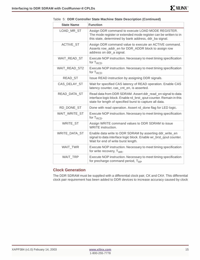
The function of each state in the DDR controller is described in Table 5.
Figure 13: DDR Controller State Machine
Table 5: DDR Controller State Machine State Description
State Name Function
IDLE Assert NOP instruction control signals to DDR. Determines next operation to execute based on the value of int_cmd signal.
AUTO_RFS_ST Assign DDR command values to execute AUTO REFRESH instruction. Auto refresh retains data in DDR SDRAM.
PRECHRG_ST Assign DDR command values to execute PRECHARGE instruction. Precharge command deactivates specified row in one bank or all banks.
IDLE LOAD_MR_ST
PRECHRG_ST
AUTO_RFS_ST
ACTIVE_ST
int_cmd = PRECHARGE
int_cmd = LOAD_MR
int_cmd = AUTO_RFS
int_cmd = READ or WRITE
WAIT_WRITE_ST
WRITE_ST
WRITE_DATA_ST
WAIT_TWR
WAIT_TRP
WAIT_READ_ST
READ_ST
CAS_DELAY_ST
READ_DATA_ST
RD_DONE_ST
WAIT_READ_ST2
int_cmd = READ int_cmd = WRITE
wr_brst_qout < 2 | 4 | 8
cas_qout < 2
rd_brst_qout < 2 | 4 | 8rd_brst_qout = 2 | 4 | 8
cas_qout = 2
wr_brst_qout = 2 | 4 | 8
X384_13_010703
14 www.xilinx.com XAPP384 (v1.0) Febuary 14, 20031-800-255-7778
Interfacing to DDR SDRAM with CoolRunner-II CPLDsR
Clock GenerationThe DDR SDRAM must be supplied with a differential clock pair, CK and CK#. This differential clock pair requirement has been added to DDR devices to increase accuracy caused by clock
LOAD_MR_ST Assign DDR command to execute LOAD MODE REGISTER. The mode register or extended mode register can be written to in this state, determined by bank address, ddr_ba signal.
ACTIVE_ST Assign DDR command value to execute an ACTIVE command. Asserts row_addr_en for DDR_ADDR block to assign row address on ddr_a signal.
WAIT_READ_ST Execute NOP instruction. Necessary to meet timing specification for TRCD.
WAIT_READ_ST2 Execute NOP instruction. Necessary to meet timing specification for TRCD.
READ_ST Issue READ instruction by assigning DDR signals.
CAS_DELAY_ST Wait for specified CAS latency of READ operation. Enable CAS latency counter, cas_cnt_en, is asserted.
READ_DATA_ST Read data from DDR SDRAM. Assert ddr_read_en signal to data interface logic block. Enable rd_brst_qout counter. Remain in this state for length of specified burst to capture all data.
RD_DONE_ST Done with read operation. Assert rd_done flag for LED logic.
WAIT_WRITE_ST Execute NOP instruction. Necessary to meet timing specification for TRCD.
WRITE_ST Assign WRITE command values to DDR SDRAM to issue WRITE instruction.
WRITE_DATA_ST Enable data write to DDR SDRAM by asserting ddr_write_en signal to data interface logic block. Enable wr_brst_qout counter. Wait for end of write burst length.
WAIT_TWR Execute NOP instruction. Necessary to meet timing specification for write recovery, TWR.
WAIT_TRP Execute NOP instruction. Necessary to meet timing specification for precharge command period, TRP.
Table 5: DDR Controller State Machine State Description (Continued)
State Name Function
XAPP384 (v1.0) Febuary 14, 2003 www.xilinx.com 151-800-255-7778
Interfacing to DDR SDRAM with CoolRunner-II CPLDsR
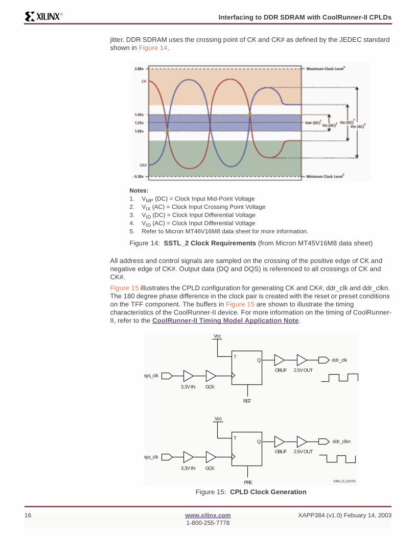
jitter. DDR SDRAM uses the crossing point of CK and CK# as defined by the JEDEC standard shown in Figure 14.
All address and control signals are sampled on the crossing of the positive edge of CK and negative edge of CK#. Output data (DQ and DQS) is referenced to all crossings of CK and CK#.
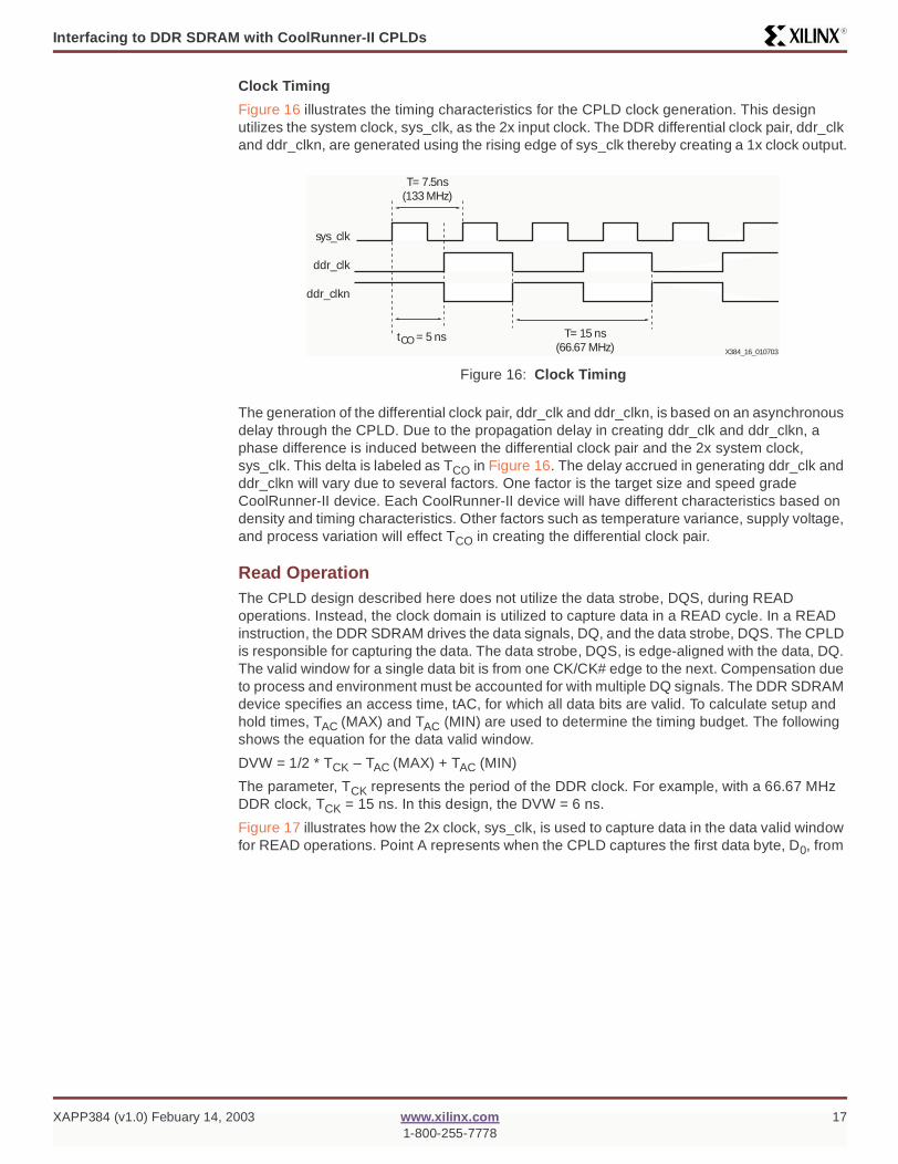
Figure 15 illustrates the CPLD configuration for generating CK and CK#, ddr_clk and ddr_clkn. The 180 degree phase difference in the clock pair is created with the reset or preset conditions on the TFF component. The buffers in Figure 15 are shown to illustrate the timing characteristics of the CoolRunner-II device. For more information on the timing of CoolRunner-II, refer to the CoolRunner-II Timing Model Application Note.
Figure 14: SSTL_2 Clock Requirements (from Micron MT45V16M8 data sheet)
Figure 15: CPLD Clock Generation
Notes: 1. VMP (DC) = Clock Input Mid-Point Voltage 2. VIX (AC) = Clock Input Crossing Point Voltage 3. VID (DC) = Clock Input Differential Voltage 4. VID (AC) = Clock Input Differential Voltage 5. Refer to Micron MT46V16M8 data sheet for more information.
X384_15_010703
TQ
RST
sys_clk
Vcc
ddr_clk
3.3V IN GCK
OBUF 2.5V OUT
PRE
ddr_clknT
Q
sys_clk
Vcc
3.3V IN GCK
OBUF 2.5V OUT
16 www.xilinx.com XAPP384 (v1.0) Febuary 14, 20031-800-255-7778
Interfacing to DDR SDRAM with CoolRunner-II CPLDsR
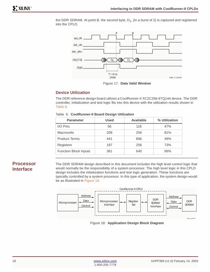
Clock Timing
Figure 16 illustrates the timing characteristics for the CPLD clock generation. This design utilizes the system clock, sys_clk, as the 2x input clock. The DDR differential clock pair, ddr_clk and ddr_clkn, are generated using the rising edge of sys_clk thereby creating a 1x clock output.
The generation of the differential clock pair, ddr_clk and ddr_clkn, is based on an asynchronous delay through the CPLD. Due to the propagation delay in creating ddr_clk and ddr_clkn, a phase difference is induced between the differential clock pair and the 2x system clock, sys_clk. This delta is labeled as TCO in Figure 16. The delay accrued in generating ddr_clk and ddr_clkn will vary due to several factors. One factor is the target size and speed grade CoolRunner-II device. Each CoolRunner-II device will have different characteristics based on density and timing characteristics. Other factors such as temperature variance, supply voltage, and process variation will effect TCO in creating the differential clock pair.
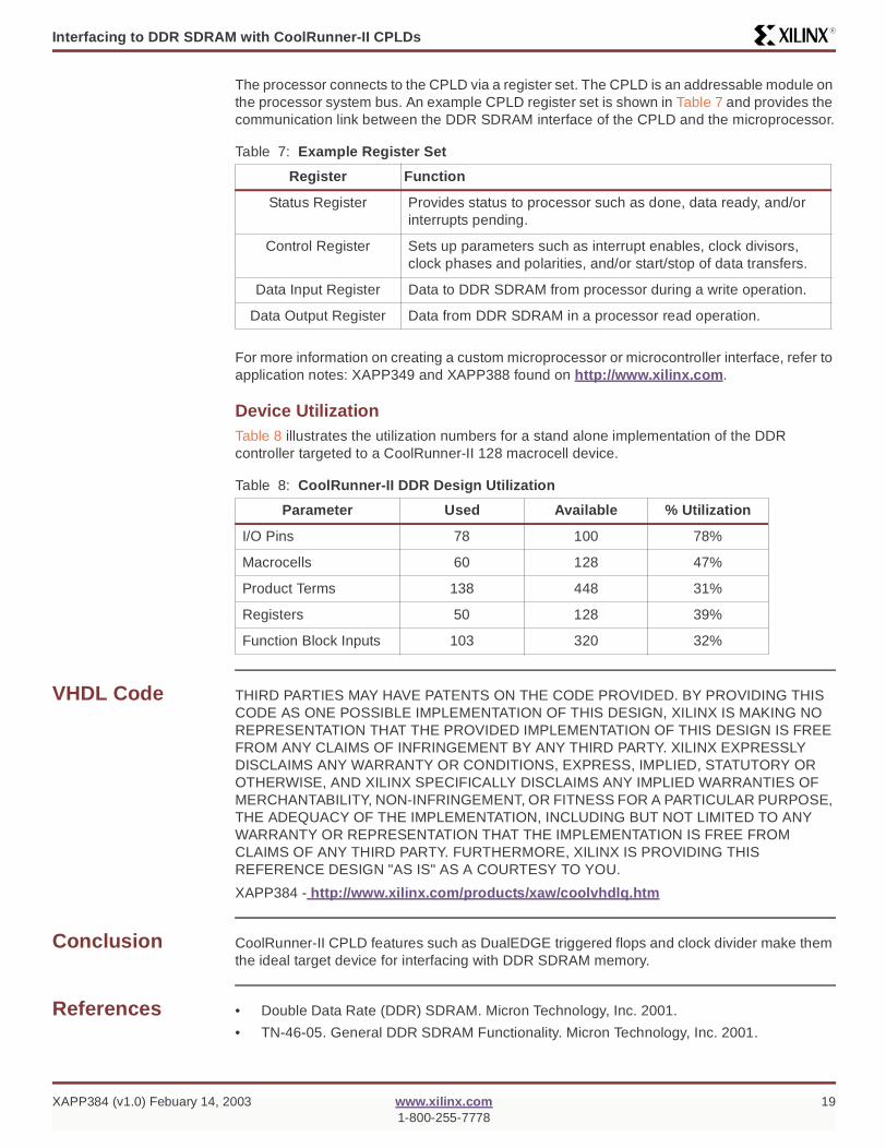
Read OperationThe CPLD design described here does not utilize the data strobe, DQS, during READ operations. Instead, the clock domain is utilized to capture data in a READ cycle. In a READ instruction, the DDR SDRAM drives the data signals, DQ, and the data strobe, DQS. The CPLD is responsible for capturing the data. The data strobe, DQS, is edge-aligned with the data, DQ. The valid window for a single data bit is from one CK/CK# edge to the next. Compensation due to process and environment must be accounted for with multiple DQ signals. The DDR SDRAM device specifies an access time, tAC, for which all data bits are valid. To calculate setup and hold times, TAC (MAX) and TAC (MIN) are used to determine the timing budget. The following shows the equation for the data valid window.
DVW = 1/2 * TCK – TAC (MAX) + TAC (MIN)
The parameter, TCK represents the period of the DDR clock. For example, with a 66.67 MHz DDR clock, TCK = 15 ns. In this design, the DVW = 6 ns.
Figure 17 illustrates how the 2x clock, sys_clk, is used to capture data in the data valid window for READ operations. Point A represents when the CPLD captures the first data byte, D0, from
Figure 16: Clock Timing
sys_clk
ddr_clk
ddr_clkn
tCO = 5 ns T= 15 ns(66.67 MHz)
T= 7.5ns(133 MHz)
X384_16_010703
XAPP384 (v1.0) Febuary 14, 2003 www.xilinx.com 171-800-255-7778
Interfacing to DDR SDRAM with CoolRunner-II CPLDsR
the DDR SDRAM. At point B, the second byte, D1, (in a burst of 2) is captured and registered into the CPLD.
Device UtilizationThe DDR reference design board utilizes a CoolRunner-II XC2C256-6TQ144 device. The DDR controller, initialization and test logic fits into this device with the utilization results shown in Table 6.
Processor Interface
The DDR SDRAM design described in this document includes the high level control logic that would normally be the responsibility of a system processor. The high level logic in this CPLD design includes the initialization functions and test logic generation. These functions are typically controlled by a system processor. In this type of application, the system design would be as illustrated in Figure 18.
Figure 17: Data Valid Window
Table 6: CoolRunner-II Board Design Utilization
Parameter Used Available % Utilization
I/O Pins 56 118 47%
Macrocells 208 256 81%
Product Terms 441 896 49%
Registers 187 256 73%
Function Block Inputs 361 640 56%
sys_clk
ddr_clk
ddr_clkn
A
T = 6 nsDVW X384_17_010703
D0 D1DQ [7:0]
DQS
B
Figure 18: Application Design Block Diagram
CoolRunner-II CPLD
Register Set
Microprocessor Interface
DDR SDRAM Interface
Address
MicroprocessorData
Control
DDR SDRAM
Address
Data
Control
X384_18_010703
18 www.xilinx.com XAPP384 (v1.0) Febuary 14, 20031-800-255-7778
Interfacing to DDR SDRAM with CoolRunner-II CPLDsR
The processor connects to the CPLD via a register set. The CPLD is an addressable module on the processor system bus. An example CPLD register set is shown in Table 7 and provides the communication link between the DDR SDRAM interface of the CPLD and the microprocessor.
For more information on creating a custom microprocessor or microcontroller interface, refer to application notes: XAPP349 and XAPP388 found on http://www.xilinx.com.
Device UtilizationTable 8 illustrates the utilization numbers for a stand alone implementation of the DDR controller targeted to a CoolRunner-II 128 macrocell device.
VHDL Code THIRD PARTIES MAY HAVE PATENTS ON THE CODE PROVIDED. BY PROVIDING THIS CODE AS ONE POSSIBLE IMPLEMENTATION OF THIS DESIGN, XILINX IS MAKING NO REPRESENTATION THAT THE PROVIDED IMPLEMENTATION OF THIS DESIGN IS FREE FROM ANY CLAIMS OF INFRINGEMENT BY ANY THIRD PARTY. XILINX EXPRESSLY DISCLAIMS ANY WARRANTY OR CONDITIONS, EXPRESS, IMPLIED, STATUTORY OR OTHERWISE, AND XILINX SPECIFICALLY DISCLAIMS ANY IMPLIED WARRANTIES OF MERCHANTABILITY, NON-INFRINGEMENT, OR FITNESS FOR A PARTICULAR PURPOSE, THE ADEQUACY OF THE IMPLEMENTATION, INCLUDING BUT NOT LIMITED TO ANY WARRANTY OR REPRESENTATION THAT THE IMPLEMENTATION IS FREE FROM CLAIMS OF ANY THIRD PARTY. FURTHERMORE, XILINX IS PROVIDING THIS REFERENCE DESIGN "AS IS" AS A COURTESY TO YOU.
XAPP384 - http://www.xilinx.com/products/xaw/coolvhdlq.htm
Conclusion CoolRunner-II CPLD features such as DualEDGE triggered flops and clock divider make them the ideal target device for interfacing with DDR SDRAM memory.
References • Double Data Rate (DDR) SDRAM. Micron Technology, Inc. 2001.
• TN-46-05. General DDR SDRAM Functionality. Micron Technology, Inc. 2001.
Table 7: Example Register Set
Register Function
Status Register Provides status to processor such as done, data ready, and/or interrupts pending.
Control Register Sets up parameters such as interrupt enables, clock divisors, clock phases and polarities, and/or start/stop of data transfers.
Data Input Register Data to DDR SDRAM from processor during a write operation.
Data Output Register Data from DDR SDRAM in a processor read operation.
Table 8: CoolRunner-II DDR Design Utilization
Parameter Used Available % Utilization
I/O Pins 78 100 78%
Macrocells 60 128 47%
Product Terms 138 448 31%
Registers 50 128 39%
Function Block Inputs 103 320 32%
XAPP384 (v1.0) Febuary 14, 2003 www.xilinx.com 191-800-255-7778
Interfacing to DDR SDRAM with CoolRunner-II CPLDsR
Revision History
The following table shows the revision history for this document.
Date Version Revision
02/05/03 1.0 Initial Xilinx release.
20 www.xilinx.com XAPP384 (v1.0) Febuary 14, 20031-800-255-7778