Embed Size (px)
Citation preview

Altera Corporation AN-348-1.1
July 2004, ver. 1.1
Interfacing DDR SDRAM withCyclone Devices
Application Note 348
Introduction Many applications use single data rate (SDR) memory. However, as these applications become more demanding, designers need to find ways to improve performance without increasing cost. Over the years, DRAM companies introduced memory types with improved architecture such as fast page mode (FPM), extended data out (EDO), and SDRAM to address this issue. Double data rate (DDR) memory is the most popular memory interface among these memory architectures because of its ability to increase data bandwidth without increasing system complexity and cost. DDR memory uses both edges of a clock to transmit data, which allows data transmission at twice the rate of a SDR memory device at the same clock speed and with the same number of I/O pins required to transmit data. DDR memory is used in many applications where fast data transmission is needed, such as memory access and first-in first-out (FIFO) memory structures. Table 1 shows the Cyclone device support for DDR SDRAM.
Cyclone™ devices can interface with DDR SDRAM at speeds up to 133 MHz or 266 Megabits per second (Mbps). This application note provides information on interfacing DDR SDRAM memory with Cyclone devices, including detailed timing analysis. This document also describes the board used to demonstrate and characterize the interface with a Cyclone device.
Functional Description
DDR SDRAM is a 2n prefetch architecture with two data transfers per clock cycle. It uses a strobe (DQS) which is associated with a group of data pins (DQ) for read and write operations. Both the DQS and DQ ports are bidirectional. Address ports are shared for write and read operations.
Table 1. DDR SDRAM Supported in Cyclone Devices
DDR Memory Type I/O Standard
Maximum Clock Rate
-6 Speed Grade Commercial Wire-Bond
-7 Speed Grade Commercial Wire-Bond
-7 Speed Grade Industrial Wire-Bond
-8 Speed Grade Commercial Wire-Bond
DDR SDRAM (1) SSTL-2 133 MHz 133 MHz 100 MHz 100 MHz
Note to Table 1:(1) These values apply when the DQS programmable delay chain is used.
1Preliminary

Interfacing DDR SDRAM with Cyclone Devices
DDR SDRAM write and read operations are sent in bursts of 2, 4, and 8. This means that you provide 2, 4, or 8 groups of data for each write transaction to receive 2, 4, or 8 groups of data for each read transaction. The time between when the read command is clocked into the memory and when the data is presented at the memory pins is called the column address strobe (CAS) latency. DDR SDRAM supports CAS latencies of 2, 2.5, and 3, depending on the operating frequency. Both the burst length and CAS latency are set in the DDR SDRAM mode register.
The DDR SDRAM specification recommends using the SSTL-2 class II I/O standard termination. Each DDR SDRAM device is divided into four banks, and each bank has a fixed number of rows and columns and can hold between 64 Mbytes to 1 Gbyte of data per JEDEC specifications. Only one row per bank can be accessed at a time. The ACTIVE command opens a row and the PRECHARGE command closes a row.
Interface Pins Table 2 lists the DDR SDRAM interface pins and how to connect them to Cyclone devices.
This section provides a description of the clock, control, address, and data signals on a DDR SDRAM device.
Clock, Strobes & Data
The DDR SDRAM device uses the CK and CK# signals to clock commands and addresses into the memory. The memory also uses these clock signals to generate the DQS signal during a read via a delay-locked loop (DLL) inside the memory. The skew between CK or CK# and the SDRAM-generated DQS signal is specified as tDQSCK in the DDR SDRAM data sheet.
Table 2. DDR SDRAM Interface Pins
Pins Description Cyclone Pin Utilization
DQ Bidirectional read and write data DQ
DQS Bidirectional read and write data strobe
DQS
CK System clock User I/O pin
CK# System clock User I/O pin
DM Optional write data mask, edge-aligned to DQ during write
DM
All other Addresses and commands User I/O pin
2 Altera CorporationPreliminary

Interface Pins
Both DQ and DQS signals are bidirectional (the same signals are used for both writes and reads). A group of DQ pins is associated with one DQS pin. In ×8 and ×16 DDR SDRAM devices, one DQS pin is associated with 8 DQ pins. Cyclone devices support both ×8 and ×16 DDR SDRAM. Use the DQS pins and their associated DQ pins listed in the Cyclone pin tables when interfacing with DDR SDRAM from Cyclone I/O banks 1, 2, 3, and 4.
See Table 3 for the number of DQS/DQ groups supported in Cyclone devices.
During a read from the memory, the data strobe signals (DQS) are edge-aligned with the data signals (DQ). During a write to the memory, the Cyclone device transmits the DQS signals center-aligned relative to the DQ signals. Figures 1 and 2 illustrate the DQ & DQS relationships during a DDR SDRAM read and write. The memory controller on the device center-aligns the DQS signal during a write and shifts the DQS signal during a read so that the DQ and DQS signals are center-aligned at the
Table 3. DQS & DQ Bus Mode Support
Device Package Number of ×8 Groups
Total DQ Pin Count
EP1C3 100-pin TQFP (1), (2) 3 24
144-pin TQFP 4 32
EP1C4 324-pin FineLine BGA® 8 (3) 64 (3)
400-pin FineLine BGA 8 (3) 64 (3)
EP1C6 144-pin TQFP 4 32
240-pin PQFP (4) 4 32
256-pin FineLine BGA 4 32
EP1C12 240-pin PQFP 4 32
256-pin FineLine BGA 4 32
324-pin FineLine BGA 8 (3) 64 (3)
EP1C20 324-pin FineLine BGA 8 (3) 64 (3)
400-pin FineLine BGA 8 (3) 64 (3)
Notes to Table 3:(1) EP1C3 devices in the 100-pin TQFP package do not have any DQ pin groups in
I/O bank 1.(2) TQFP: thin quad flat pack.(3) Although these devices have 8 DQS and 64 DQ pins, due to limited clock
resources, you may not be able to use all of them to interface with DDR memory. Depending on your design, some of these pins may be used for other purposes.
(4) PQFP: plastic quad flat pack.
Altera Corporation 3Preliminary

Interfacing DDR SDRAM with Cyclone Devices
capture register. The Cyclone device uses a phase-locked loop (PLL) to center-align the DQS signal with respect to DQ signals during writes and uses dedicated DQS programmable delay chain circuitry to shift the incoming DQS signal during reads.
Figure 1. DQ & DQS Relationship During DDR SDRAM Read
Figure 2. DQ & DQS Relationship During DDR SDRAM Write
The setup (tDS) and hold (tDH) times for the DQ and data mask (DM) pins during a write are relative to the edges of DQS write signals and not the CK and CK# clocks. The setup and hold times are equal (tDS = tDH) and are typically 0.5 ns for a 133-MHz DDR SDRAM device.
The DDR SDRAM tDQSS timing is the time between when the memory detects the write command to the first DQS transition. The DQS signal is normally generated on the positive edge of system clock to meet the tDQSS requirement. The DQ and DM signals are clocked using a –90° shifted clock from the system clock. The edges of the DQS signal are centered on the DQ and DM signals when they arrive at the DDR SDRAM device.
DQS at DQLE registers
DQS at FPGA Pin
DQ at DQLE registers
DQ atFPGA Pin
Pin to registerdelay
Pin to registerdelay
90 degree shift
Preamble Postamble
DQS atFPGA Pin
DQ atFPGA Pin
4 Altera CorporationPreliminary

Interface Pins
To minimize the skew between the arrival time of these signals, the DQS, DQ, and DM board trace lengths should be similar.
The DDR SDRAM tDQSS write requirement states that on writes, the positive edge of the DQS signal must be within ±25% (±90°) of the positive edge of the DDR SDRAM clock input. Therefore, you should use the logic element (LE) registers to generate the CK and CK# signals. This will help match the CK and CK# signals with the DQ signal as well as reduce any process, voltage, temperature variations, and skew between CK or CK# and DQ signals.
DM Pins
DDR SDRAM uses the DM pins during the write operation. A low signal on the DM pin indicates that the write is valid. If the signal on the DM pin is high, the memory will mask the DQ signals. In Cyclone devices, the DM pins are pre-assigned in the device pin outs. Altera recommends using these pre-assigned pins for the DM pins, although you can use any of the I/O pins in the same bank as the DQS and DQ pins to generate the DM signal.
The timing requirements for DM signals at the DDR SDRAM are identical to those of the DQ output signals. Similarly, the DM signals are clocked out by the –90° shifted clock.
Commands & Addresses
Commands and addresses in DDR SDRAM devices are clocked into the memory using the CK and CK# signal at the single data rate using only one clock edge. DDR SDRAM devices have 12 to 14 address pins, depending on the device capacity. The address pins are multiplexed, so two clock cycles are required to send the row, column, and bank addresses. The CS, RAS, CAS, and WE pins are DDR SDRAM command pins.
The DDR SDRAM address and command inputs both require the same setup and hold times with respect to the DDR SDRAM clock. The Cyclone device address and command signals change at the same time as the DQS write signal since they are both generated from the system clock. The positive edge of the DDR SDRAM clock, CK, is aligned with the DQS signal to satisfy tDQSS. If the command and address outputs are generated on the clock's positive edge, they may not meet the setup time requirements (see Figure 5). Therefore, you should use the negative edge of the system clock for the commands and addresses to the DDR SDRAM. You can use any of the I/O pins for the commands and addresses.
Altera Corporation 5Preliminary

Interfacing DDR SDRAM with Cyclone Devices
Figure 3 shows the address and command timing and the DDR SDRAM tDQSS, tDS, and tDH timing requirements.
Figure 3. Address & Command Timing Notes (1), (2)
Notes to Figure 3:(1) The address and command timing shown in Figure 3 is applicable for both reads and writes.(2) If the board trace lengths for the DQS, CK, address, and command pins are the same, the signal relationships at the
Cyclone device pins are maintained at the DDR SDRAM pins.
Read Side Implementation Using DQS Programmable Delay Chain Circuitry
Cyclone devices have DQS programmable delay chain circuitry on each DQS pin that allows a phase shift to center-align the input DQS synchronization signals within the data window of their corresponding DQ data signals at the LE register. This ensures the data will be latched at the LE register. The phase-shifted DQS signals drive the global clock network, which in turn clocks the DQ signals on internal LE registers. The DQS signal is inverted before going to the DQ LE clock ports.
Figure 4 shows how the Cyclone device generates the DQ, DQS, CK, and CK# signals. The write PLL generates the system clock and –90° shifted clock (write clock). The write PLL's input clock frequency is not required to be the same as the DDR SDRAM frequency of operation. The system clock and write clock have the same frequency as the DQS frequency, but the write clock is shifted –90° from the system clock.
System Clock
CK at CycloneDevice Pin
DQS Write at FPGA Pin
Address/Command Pins (positive edge)
Address/Command Pins(negative edge)
DQS Write at SDRAM
SDRAM Write Requirement
Address/Command Pinsat SDRAM (negative edge)
SDRAM Address/CommandInput Timing to the DDR
SDRAM Device
tSU
tDQSS
tCO
tCO
tH
6 Altera CorporationPreliminary

Read Side Implementation Using DQS Programmable Delay Chain Circuitry
Figure 4. DDR SDRAM with DQS Phase-Shift Circuitry
Notes to Figure 4:(1) DQ and DQS signals are bidirectional. One DQS signal is associated with a group of DQ signals.(2) Although there are three LE registers for capturing the read data, this figure only shows one register.(3) The clock to this register can either be the system clock or another clock output of the write PLL. If the design needs
another write PLL clock output, another register is needed to transfer the data back to the system clock domain.
Figure 5 shows a detailed picture of the Cyclone device read data path for ×8 mode. The DQS signal goes to the DQS programmable delay chain circuitry and is center-aligned. The shifted DQS signal is then routed to
Write PLL
DDR
DDR
CK and CK#
DQS "Read" (1)
DQ "Read" (1)
input_clk
DQ "Write" (1)
length = l2
length = l2
length = l1
length = l2
DQS "Write" (1)
length = l2
length = l2
DDR
DDR
DFF(2)
DFF
DQS ProgrammableDelay Chain Circuitry
(3)
SystemClock
WriteClock
DM
DDR SDRAMCyclone Device
Altera Corporation 7Preliminary

Interfacing DDR SDRAM with Cyclone Devices
the global clock network. The DQS signal is then inverted before it clocks the DQ at the LE registers. The outputs of the input LE registers then go to the resynchronization registers. The resynch_clk signal clocks the resynchronization register. The resynch_clk signal can come from the system clock, the write clock, or the write PLL clock. Registers AI, BI, and CI are the capture registers, and registers D and E are the resynchronization registers.
Figure 5. DDR SDRAM Read Data Path in Cyclone Devices
Notes to Figure 5:(1) Registers D and E are resynchronization registers.(2) Registers AI, BI, and CI are capture registers.
DQS Postamble
The DDR SDRAM DQ and DQS pins use the SSTL-2 class II I/O standard. When the Cyclone and the DDR SDRAM devices do not drive the DQ and DQS pins, the signals go to a high-impedance state. Since a pull-up resistor terminates both DQ and DQS to VTT (1.25 V), the effective voltage
dqs_oe
dq_oe
dqs_out
dq_out
D Q
D Q
DQ
DQ DQ
dq[7..0]
dqs
dqsLocalBus
D
E
resynch_clk
dataout[15..0]
∆t
ProgrammableDelay Chain
IOELE
Register E (1) Register AI (2)
Register D (1) Register CI (2) Register BI (2)
8 Altera CorporationPreliminary

Read Side Implementation Using DQS Programmable Delay Chain Circuitry
on the high-impedance line is 1.25 V. According to the JEDEC JESD 8-9 specification for SSTL-2 I/O standard, this is an indeterminate logic level and the input buffer can interpret this as either a logic high or logic low. If there is any noise on the DQS line, the input buffer may interpret that noise as actual strobe edges. Therefore, when the DQS signal goes to a high-impedance state after a read postamble, you should disable the input LE registers so that erroneous data does not get latched in and all the data from the memory are resynchronized properly.
Figure 6 shows a read operation example when the DQS postamble could be a problem. Figure 6 shows the output waveforms of LE registers AI, BI, CI, D and E. Waveform AI shows the output of register AI. Waveform BI shows the output of register BI. The output of register CI goes into the register whose output is shown in waveform CI. Waveforms D and E show the output signals after the resynchronization registers.
Figure 6. Read Example with a DQS Postamble Issue
Q0H Q0L Q1H
Q0H
Q0H
Q0L
Q1H
Q1L
Q0H Q0L Q1H Q1L
Q0L Q1L
Q0H Q1H
DQSat the pin
DQSat the LE
DQat the pin
DQat the LE
A
B
C
resynch_clock
D
E
0 ns 5 ns 10 ns 15 ns 20 ns 25 ns
Altera Corporation 9Preliminary

Interfacing DDR SDRAM with Cyclone Devices
The first falling edge of the DQS at the LE register occurs at 10 ns. At this point, data Q0H is clocked in by register BI (waveform BI). At 12.5 ns, data Q0L is sampled in by register AI (waveform AI) and data Q0H passes through register CI (waveform CI). In this example, the positive edge of the resynch_clk occurs at 16.5 ns, where both Q0H and Q0L are sampled by the LE’s resynchronization registers. Similarly, data Q1H is clocked in by register BI at 15 ns, while data Q1L is clocked in by register AI and data Q1H passes through the register at 17.5 ns. At 20 ns, assume that noise on the DQS line causes a valid clock edge at the LE registers such that it changes the value of waveforms AI, BI, and CI. The next rising edge of the resynch_clk signal does not occur until 21.5 ns, but data Q1L and Q1H are not valid anymore at the output of register AI and register CI, so the resynchronization registers do not sample Q1L and Q1H and may sample the wrong data instead.
Cyclone devices have non-dedicated logic that can be configured to prevent a false edge trigger at the end of the DQS postamble. Each Cyclone DQS signal is connected to postamble logic that consists of a D flip flop (see Figure 7). This register is clocked by the shifted DQS signal. Its input is connected to ground. The controller needs to include extra logic to tell the reset signal to release the preset signal on the falling DQS edge at the start of the postamble. This disables any glitches that happen right after the postamble. This postamble logic is automatically implemented by the Altera® MegaCore® DDR SDRAM Controller in the LE register as part of the open-source datapath.
10 Altera CorporationPreliminary

Read Side Implementation Using DQS Programmable Delay Chain Circuitry
Figure 7. Cyclone DQS Postamble Circuitry Connection
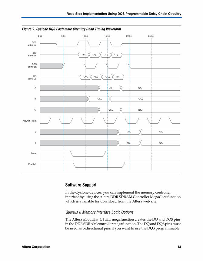
Figure 8 shows the timing waveform for Figure 7. Figure 9 shows the read timing waveform when the Cyclone DQS postamble logic is used. When the postamble logic detects the falling DQS edge at the start of postamble, it sends out a signal to disable the capture registers to prevent any accidental latching.
D Q
ENA
Q DPRN
CLRN
D Q
ENA
D Q
ENA
∆t
PostambleLogic
EnableN
Reset
GlobalClock Network
DQ[7..0]
DQS
DQS ProgrammableDelay Chain
Circuitry
DQS'
Capture Register
Capture RegisterCapture Register
Altera Corporation 11Preliminary

Interfacing DDR SDRAM with Cyclone Devices
Figure 8. Cyclone DQS Postamble Circuitry Control Timing Waveform
DQS
DQS'
Reset
EnableN
12 Altera CorporationPreliminary
Read Side Implementation Using DQS Programmable Delay Chain Circuitry
Figure 9. Cyclone DQS Postamble Circuitry Read Timing Waveform
Software Support
In the Cyclone devices, you can implement the memory controller interface by using the Altera DDR SDRAM Controller MegaCore function which is available for download from the Altera web site.
Quartus II Memory Interface Logic Options
The Altera altddio_bidir megafunction creates the DQ and DQS pins in the DDR SDRAM controller megafunction. The DQ and DQS pins must be used as bidirectional pins if you want to use the DQS programmable
Q0H
Q0H
Q0L
Q1H
Q1L
Q1H
Q0L Q1L
Q0H Q1H
AI
BI
CI
resynch_clock
D
E
Reset
EnableN
0 ns 5 ns 10 ns 15 ns 20 ns 25 ns
Q0H Q0L Q1H Q1L
Q0H Q0L Q1H Q1L
DQSat the pin
DQSat the LE
DQat the pin
DQat the LE
Altera Corporation 13Preliminary

Interfacing DDR SDRAM with Cyclone Devices
delay circuitry. You must set the DQS frequency and DQS delay logic options in the Quartus® II Assignment Editor to use the DQS programmable delay circuitry.
The DQS delay logic option allows you to set the delay in terms of time units. This option needs to be applied to a bidirectional pin with a valid DQS frequency.
The programmable delay is preset to 64 possible delay settings according to Figure 10. When a delay time is set, the Quartus II software chooses the optimum setting from these 64 possible delay settings that will result in a delay closest to the delay time assigned. Figure 10 shows the 64 settings versus time and does not show the actual delay implemented in the Quartus II software.
Figure 10. DQS Delay vs. DQS Settings
The DQS frequency should be set to the frequency of the incoming DQS signal. This option is ignored if it is applied to anything other than pins intended for use with the dedicated DDR SDRAM interface.
f For more information on the altddio_bidir megafunction, see the Altera Double Data Rate Megafunctions User Guide.
14 Altera CorporationPreliminary

Read Side Implementation Using DQS Programmable Delay Chain Circuitry
DDR SDRAM Controller MegaCore Function
The DDR SDRAM Controller MegaCore function allows you to instantiate a simplified interface to industry-standard DDR SDRAM memory. The DDR SDRAM Controller initializes the memory devices, manages SDRAM banks, and keeps devices refreshed at appropriate intervals. The MegaCore function translates read and write requests from the local interface into all the necessary SDRAM command signals.
The DDR SDRAM Controller is optimized for Cyclone devices and provides features to implement DQS postamble control logic and automatic constraint files for LE placement within Cyclone devices. The advanced features available in these devices allow you to interface directly to DDR SDRAM devices and to use the DQS signal in the read and write direction. Figure 11 shows the Altera DDR SDRAM Controller block diagram. The DDR SDRAM Controller contains encrypted control logic as well as an open source data path that you can use for your design.
Figure 11. DDR SDRAM Controller System Level Block Diagram
Note to Figure 11:(1) You can either use the encrypted control logic or provide your own controller logic in the DDR SDRAM Controller
function.
The example instance instantiates a PLL, an example driver, and your DDR SDRAM Controller custom variation as shown in Figure 11. The example instance is a fully functional design that can be simulated, synthesized, and used in hardware. The example driver issues read and write commands to the controller and checks the read data to produce the pass/fail and test complete signals. If you do not want to use the DDR SDRAM Controller encrypted control logic, you can replace it with your
ControlLogic
(Encrypted)
Data Path(Open
Source)
DDR SDRAM
Example Driver
PLL
LocalInterface
DDR SDRAMInterface
DDR SDRAM Controller
Passor fail
InputClock
(1)
Cyclone Device
Altera Corporation 15Preliminary

Interfacing DDR SDRAM with Cyclone Devices
own custom logic. This allows you to use the Altera data path with your own logic. Figure 12 shows the data path for the interface between a Cyclone device and DDR SDRAM.
Figure 12. Data Path
D Q D Q
D Q
D Q
D QD Q
D QD Q
D Q
Q D
Q D
dclng_wr
write_clk
wdata
wdata_valid
resynch_clk
rdata
postamble_clk
dclng_wr
te
wdata_valid
write_clk
dq_oe
D Q
D Q
Q D
Q DQ D
D Q
D Q
D Q
D Q
D Q
EN
EN
EN
EN
D Q
D Q
D Q
DDR SDRAM
Cyclone Device
DQS ProgrammableDelay Chain
Circuitry
dqs
dm
dq ddr_dq[16..0]
ddr_dqs[1..0]
ddr_dm [1..0]
write_clk
dq_enable
Preset(Asynchronous)dq_enable_reset
16
16 8
8
8
8
DQS_AOEdqs_oe
EN
EN
IOEs
LEs
BOE
BI
CI
AI
AO
BO
DQ_AOE
EN
16 Altera CorporationPreliminary

Read Side Implementation Using DQS Programmable Delay Chain Circuitry
f For more information on the Altera DDR SDRAM Controller, see the DDR SDRAM Controller MegaCore Function User Guide.
Read Margin Analysis
Table 4 shows the worst case DDR SDRAM read timing margin analysis at 100 and 133 MHz, when the board trace variations for the DQ and DQS pins is ±50 ps (approximately ±0.3-inches of FR4 trace length variations). You can perform a similar timing analysis for your interface with another DDR SDRAM memory by replacing the tHP, tQHS, and tDQSQ values in Table 4 with those from your memory data sheet.
Table 4. Example Read Timing Analysis When Using DQS Circuitry in Cyclone -6 Speed-Grade Devices (Part 1 of 2)
Parameter Specification 100 MHz (1) 133 MHz (1) Description
Memory specifications
tH P 4.50 ns 3.38 ns Half period as specified by the memory data sheet
tQ H S 0.75 ns 0.75 ns Data hold skew factor as specified by the memory data sheet
tD Q S Q 0.5 ns 0.50 ns Skew between DQS and DQ from the memory
tQ H 3.75 ns 2.63 ns Data valid window (tH P – tQ H S)
FPGA specifications
tD C (2) 2.16 ns 1.6 ns Ideal programmable delay chain setting
tD C E R R 0.3 ns 0.3 ns DQS variations due to programmable delay circuitry
tD Q S 2 L E _ M I N (3) 1.033 ns 1.033 ns Minimum DQS pin to LE register delay
tD Q S 2 L E _ M A X (3) 1.932 ns 1.932 ns Maximum DQS pin to LE register delay
tD Q 2 L E _ M I N (3) 1.017 ns 1.017 ns Minimum DQ pin to LE register delay
tD Q 2 L E _ M A X (3) 2.003 ns 2.003 ns Maximum DQ pin to LE register delay
tD Q S Q I N T 0.07 ns 0.07 ns Internal skew between DQS and DQ inside Cyclone devices
µtS U 0.04 ns 0.04 ns Intrinsic setup time of the LE register (rounded up)
µtH 0.02 ns 0.02 ns Intrinsic hold time of the LE register (rounded up)
Board specification
tE X T ±0.05 ns ±0.05 ns Board trace variations on the DQ and DQS lines
Altera Corporation 17Preliminary

Interfacing DDR SDRAM with Cyclone Devices
In order to achieve the optimum sampling window, you must calculate the amount of delay for DQS signal, tDC. To account for the PVT variation of the programmable delay chain, add tDCERR to tDC.
tSHIFT(max) = tDC + tDCERR
tSHIFT(min) = tDC – tDCERR
Timing calculations
tS H I F T _ M I N 1.86 ns 1.30 ns Minimum shift provided by the DQS phase-shift circuitry (tD C – tD C E R R)
tS H I F T _ M A X 2.46 ns 1.90 ns Maximum shift provided by the DQS phase-shift circuitry (tD C + tD C E R R)
tD E LTA _ M I N 1.876 ns 1.316 ns Minimum difference between the DQS and the DQ signal paths (tD Q S 2 L E _ M I N + tS H I F T _ M I N – tD Q 2 L E _ M I N)
tD E LTA _ M A X 2.389 ns 1.829 ns Maximum difference between the DQS and the DQ signal paths (tD Q S 2 L E _ M A X + tS H I F T _ M A X – tD Q 2 L E _ M A X)
Results Read setup timing margin
1.216 ns 0.656 ns tD E LTA _ M I N– tD Q S Q – tE X T – tD Q S Q I N T – µtS U
Read hold timing margin
1.241 ns 0.661 ns tQ H – µtH – tE X T – tD Q S Q I N T – tD E LTA _ M A X
Notes to Table 4:(1) The memory numbers used here come from Micron MT46V16M8TG/MT46VV8M16TG devices. The -75 speed
grade is used for 100 and 133 MHz.(2) This timing calculation is based on equal setup and hold slack.(3) These numbers are from the Quartus II software, version 4.0. Altera recommends using the latest version of the
Quartus II software for your design.
Table 4. Example Read Timing Analysis When Using DQS Circuitry in Cyclone -6 Speed-Grade Devices (Part 2 of 2)
Parameter Specification 100 MHz (1) 133 MHz (1) Description
18 Altera CorporationPreliminary

Read Side Implementation Using DQS Programmable Delay Chain Circuitry
Table 5 shows the DQS and DQ path delays to the LE registers when the programmable delay chain is set to zero delay and the LE registers are placed using the constraint files provided by the DDR SDRAM Controller.
In Figure 13, the setup slack time is:
setup slack time = minimum DQS shift – minimum DQ shift – µtSU = [tSHIFT(min) + tDQS2LE(min)] – [tDQ2LE(min) + tDQSQ + tEXT + tDQSQINT] – µtSU
Similarly, the hold slack time is:
hold slack time = maximum DQ shift – maximum DQS shift – µtH = [tDV_MEM + tDQ2LE(max) + tDQSQ – tEXT – tDQSQINT] – [tSHIFT(max) – tDQS2LE(max)] – µtH
= [tQH + tDQ2LE(max) – tEXT – tDQSQINT] – [tSHIFT(max) – tDQS2LE(max)] – µtH
If you set the setup slack time to equal the hold slack time, you can find the amount of DQS delay needed to achieve even setup and hold slack.
Table 5. DQS & DQ Internal Delay Note (1)
Specification
Internal Delay (ns)
Description-6 Speed Grade Commercial Wire-Bond
-7 Speed Grade Commercial Wire-Bond
-7 Speed Grade Industrial Wire-Bond
-8 Speed Grade Commercial Wire-Bond
tD Q S 2 L E (minimum)
1.033 1.033 1.033 1.033 Minimum internal delay from DQS pad to LE register
tD Q S 2 L E (maximum)
1.932 2.223 2.513 2.513 Maximum internal delay from DQS pad to LE register
tD Q 2 L E (minimum)
1.017 1.017 1.017 1.017 Minimum internal delay from DQ pad to LE register
tD Q 2 L E (maximum)
2.003 2.304 2.606 2.606 Maximum internal delay from DQ pad to LE register
Note to Table 5:(1) These numbers are from the Quartus II software version 4.0. For the latest numbers, check the latest version of the
Quartus II software.
Altera Corporation 19Preliminary

Interfacing DDR SDRAM with Cyclone Devices
tDC = 0.5 × tQH + tDQSQ + µtSU – µtH + [tDQ2LE(max) + tDQ2LE(min)] – [tDQS2LE(max) + tDQS2LE(min)]
Using the results from Tables 4 and 5, for the 133-MHz DDR SDRAM memory,
tDC = 0.5 × 2.63 + 0.5 + 0.04 – 0.02 + [2.003 + 1.017] – [1.932 + 1.033] = 1.6 ns
Therefore, the correct phase shift needed for the 133-MHz DDR SDRAM memory will be
correct phase shift = (1.6/7.5) × 360° = 77°
This shows that phase shift required to center DQS within DQ is not exactly 90°.
The Altera DDR SDRAM Controller MegaCore function automatically sets the DQS delay for an optimum data capture window.
Figure 13. DQS & DQ Signals
DQS
DQ
DQS
DQ
DQS
DQ
tDQSQ
tEXT + tDQSQ
tDQ2LE µtSU µtH
Data ValidWindow
tSHIFT + tDQS2LE
tQH
Setup Slack Hold Slack
At the DDRSDRAM Device
At theCyclone FPGA
At the CycloneFPGA LE Register
20 Altera CorporationPreliminary

Read Side Implementation Using DQS Programmable Delay Chain Circuitry
Round-Trip Delay
Figure 14 shows the timing analysis and the round-trip delay. The round-trip delay is the delay from the Cyclone device clock to the DDR SDRAM and back to the Cyclone device (input to register C). The analysis is required to reliably transfer data from the register B to register C.
Figure 14. Round-Trip Delay
Register A in Figure 14 represents the DDR capture logic. The Q output from register A represents the point which the read data has been converted from DDR to SDR. At the output of register A, the data is already at single data rate, but is still in the DQS clock domain. Register B aligns the single data rate data. QH (DQ data during DQS high) is
Q D
PLL
Cyclone Device DDRSDRAM
DQS Read
clk
clk_shifted
clk_to _sdram
tPD (DQS Trace)
c1
c0
D Q
D Q
D Q
Q D
D Q
DQ Read
DQS Write
Address/Command Pins
clock_source
DQ
CLKFPGA CLK
tCQ (Capture)tPD (Capture)
tPD (Capture)
tPD (Clock Trace)
tDQSCK (Read)
tDQSS (Write)
tPD (clk to pin)
tPD (clk_ext to pin)
tCQ (DQS Write)
tPD (Capture) tCQ (Capture)
B A
(A)
(B) (C)
(D)
(E)
(F)(G)
(H)(I)data_out Q D
C
(K) (J)
Delay
Altera Corporation 21Preliminary

Interfacing DDR SDRAM with Cyclone Devices
sampled on the positive edge of the 90° phase-shifted DQS pulse, but re-sampled on the negative edge of the 90° phase-shifted DQS pulse, to align it with QL (DQ data during DQS low). See Figure 9 for the waveform.
Once sampled on the negative edge of the center-aligned DQS pulse, QL and QH are available for resynchronization.
To sample the Q output of register B into register C, you need the timing relationship between register C’s clock input and the D input, which depends on the phase relationship between DQS and the system clock. Use the following steps to calculate the relationship between register C’s clock input and the D input:
1. Calculate the system’s round-trip delay.
2. Select a resynchronization phase of the system clock or other available clock that reliably samples the Q output of register A, based on the calculated safe resynchronization window. See Figure 15.
3. Apply the correct clock edge for your resynchronization logic in your memory controller.
You can use the clk or clk_shifted signals as the register C clock input. You can invert the clk and clk_shifted signals if needed. To determine the timing of data at the D input of register C relative to system clock, consider the following timing-path dependencies, which are in chronological order:
The DDR SDRAM clock input arrives (a delayed version of clk) DQS strobe from the DDR SDRAM arrives at the clock input of
register A Data arrives at the Q output of register A Data arrives at the D input of register B Data arrives at the Q output of register B Data arrives at the D input of register C
There are three main delays to this path:
Clock delays between the FPGA global clock net and the DDR SDRAM clock input
DQS strobe delays between the DDR SDRAM clock input and arrival of the DQS signal at the FPGA capture registers
Read data delays between the output of register A and the input of register C
22 Altera CorporationPreliminary

Read Side Implementation Using DQS Programmable Delay Chain Circuitry
Figure 14 shows the individual delays between points (A) and (K). The round-trip delay is the sum of all the individual delays. Figure 15 shows the timing relationship of the signals for the delays between points (A) to (I) for a CAS latency of 2.5.
Altera Corporation 23Preliminary

Interfacing DDR SDRAM with Cyclone Devices
Figure 15. Round-Trip Delay Calculation
Notes to Figure 15:(1) The letters in parenthesis refer to the letters in Figure 14.(2) The DQS strobe edge can be anywhere within ±tDQSCK of the DDR SDRAM clock pin edge. Figure 14 assumes the
DQS strobe occurs tDQSCK time after the clock for the maximum round-trip delay calculation and occurs tDQSCK time before the clock for minimum round-trip delay calculation.
(3) The delays in the DQS path from the FPGA pin to the capture register are matched to the delays for the DQ path with the exception of the DQS delay chain.
(4) Although data is initially sampled at a capture register on the positive edge of DQS, QH and QL are only available on the negative edge in SDR at the Q outputs of the DDR capture logic.
clk (A)
Round-Trip Delay
tPD (clk to pin)
FPGA CLK Pin (B)
tPD (Clock Trace)
SDRAM CLK Pin (C)
tDQSCK
SDRAM DQS Pin (D)(during Read
CL = 2.5) tPD (DQS Trace)
tPD (Capture)
FPGA DQS Pin (E)
90˚
90˚ DQS phase shift (F)
Clock input at Register A (G)
tCQ (Capture)
Q Output of Register A (H)
tPD (Routing)
D Inputof Register B (I)
Q Output of Register B (J)
D Inputof Register C (K)
ResynchronizationPhase
Clock
DQSStrobe
CapturedDQ Data
tCQ (Capture)
tPD (Routing)
(2)
(3)
(4)
24 Altera CorporationPreliminary

Read Side Implementation Using DQS Programmable Delay Chain Circuitry
To determine the point at which the data can be reliably resynchronized, calculate the minimum and maximum round-trip delay. You can then determine what resynchronization logic to use for your system. Make sure to take PVT variations into account.
Delay (A) to (B) is the clock-to-output time to generate the clock signals to the DDR SDRAM device.
Delay (B) to (C) is the trace delay for the clock. If there are multiple devices in the system, use the one furthest away from the FPGA for the maximum calculation and the one closest to the FPGA for the minimum calculation.
Delay (C) to (D) is the relationship between the clock and the DQS strobe timing during reads. The tDQSCK time in DDR SDRAM specifications is nominally 0, but varies by ±0.75 ns depending on the DDR SDRAM device speed grade. The DQS output strobe is guaranteed to be within ±tDQSCK of the clock input. Use tDQSCK(maximum), typically +0.75 ns, to calculate the maximum round-trip delay and use tDQSCK(minimum), typically –0.75 ns, to calculate the minimum delay.
Delay (D) to (E) is the trace delay for DQS, which typically matches the trace delay for the DQ signals in the same byte group. To calculate the maximum round-trip delay, use the byte group with the longest trace lengths. Use the byte group with the shortest trace lengths to calculate the minimum round-trip delay. Similarly, if there are multiple devices in the system, use the one furthest from the FPGA for the maximum calculation and the one closest to the FPGA for the minimum. Trace lengths between different byte groups do not have to be tightly matched, but a difference between the longest and shortest decreases the safe resynchronization window, the window size within which the data can be reliably resynchronized.
PLL jitter, clock duty cycle, and the half cycle used to align QH and QL also affect the round-trip delay. You must add each of these delays to the maximum round-trip delay and subtract them from the minimum round-
Altera Corporation 25Preliminary

Interfacing DDR SDRAM with Cyclone Devices
trip delay. The PLL jitter and clock duty cycle are not show in Figure 15, but are included in Table 6 which shows example round-trip delay calculations.
Resynchronization Selections
When the DQS signal arrives at the Cyclone device, the programmable delay chain center-aligns the signal to capture the DQ signals. The signals are then ready to be synchronized with the system clock. The round-trip delay numbers vary depending on the board delay and the device internal delay. Complete a timing analysis to decide whether to use the falling edge or rising edge of the system clock or the write clock for the synchronization registers. After calculating the maximum and minimum round-trip delay, determine the equivalent number of system clock cycles
Table 6. Example Round-Trip Delay Calculations Note (1)
Delay Trace Lengths in Figures 14 & 15
Example Minimum Values (ns)
Example Maximum Values (ns) Comments
tP D (clk to pin) (A) to (B) 2.00 3.00 Equal to tC Q (DQS write)
tP D (clock trace) (B) to (C) 0.33 0.50 2 to 3 inches at 166 ps per inch (2)
tD Q S C K (C) to (D) –0.75 + 0.75 See DDR SDRAM specifications
tP D (dqs trace) (D) to (E) 0.33 0.50 2 to 3 inches at 166 ps per inch (2)
90° phase-shift (E) to (F) 1.30 1.90 Includes Cyclone PLL jitter and phase-shift error
tP D (capture) (F) to (G) 1.00 2.00
tC Q (capture) (G) to (H) 0.00 0.20
tP D (routing) (H) to (I) 0.30 0.60
tC Q (capture) (I) to (J) 0.00 0.20
tP D (routing) (J) to (K) 0.30 0.60
Alignment time (3) - 3.75 3.75 Half clock period
PLL jitter - –0.30 + 0.30 PLL jitter specification
Clock duty cycle - –0.38 + 0.38 45-55% duty at 133 MHz
Round-trip total (A) to (K) 7.88 14.68
Notes to Table 6:(1) These numbers are from an example design and are not taken from a specific system or a specific device. (2) To determine your system’s exact delay, perform a time domain reflectrometry (TDR) analysis on your system.(3) The half period is because the DDR-capture registers transfer the data to the resynchronization register on the
falling edge of the shifted and inverted DQS signal.
26 Altera CorporationPreliminary

Read Side Implementation Using DQS Programmable Delay Chain Circuitry
at your operating frequency to find the point at which the data becomes valid relative to the system clock. The example maximum delay in Table 6 represents 1.96 cycles at 133 MHz, and the minimum represents 1.05 cycles. If the CAS latency is included, which is equal to 2.5 in Figure 16, the example represents a minimum delay of 3.55 cycles and a maximum delay of 4.46 cycles.
The overlap of the minimum and maximum data valid windows defines the data valid window, which is the safe resynchronization window and µtSU and µtH of register B.
Figure 16 shows an example of the round-trip delay analysis.
Figure 16. Round-Trip Delay Diagram Example 1 Note (1)
Note to Figure 16:(1) T refers to the system clock period, which is 7.5 ns in this example.
The round-trip delay helps you determine the safe resynchronization window and how to resynchronize the data. Since the shifted DQS signal goes into the LEs for resynchronization within the LE, this means that the DQS clock domain to system clock domain transfer happens between two LE registers.
System clock
CK at theFPGA
DQS at theFPGA
DQS at theLE input ports
DQ at theLE input ports
DQ at the LE outputports (maximum)
DQ after theresynchronization
DQ at the LE outputports (minimum)
CLK at thememory
DQS at thememory
time = 0 s time = 3.55T
time = 4.46T
time = 4.55T
Safe Resynchronization Window
Minimum Round-Trip Delay +CAS Latency + 0.5 Period
Maximum Round-Trip Delay + CAS Latency + 0.5 Period
System Clock EdgeUsed for Resynchronization
Altera Corporation 27Preliminary

Interfacing DDR SDRAM with Cyclone Devices
Assume the time 0 is the time of the clock rising edge. Once the DDR SDRAM device receives this rising edge from the Cyclone device, the read command is clocked into the SDRAM upon receiving this positive edge, and you can calculate the safe resynchronization window valid time as follows:
Minimum safe resynchronization window valid time = maximum round-trip delay + CAS latency × clock period + µtSU
Maximum safe resynchronization window valid time = minimum round-trip delay + (CAS latency + 1) × clock period – µtH
The size of your safe resynchronization window should be larger than 70 ps to accommodate worst case clock skew between two PLL output clocks, which is 70 ps.
From the example in Table 6, the minimum safe resynchronization window valid time is 4.46 cycles and the maximum safe resynchronization window valid time is 4.55 cycles (if µtSU and µtH is ignored).
The size of the safe resynchronization window in the example is then 0.1 cycles, calculated by the following by the following equation:
Safe resynchronization window size = maximum safe resynchronization window valid time –minimum safe resynchronization window valid time
Next, determine how many half clock cycles elapse from time 0 to the minimum safe resynchronization window valid safe resynchronization window (numcycle) by calculating the ceiling function of the minimum safe resynchronization window valid time divided by the time elapsed in half a clock cycle. To find out whether the safe resynchronization window falls within a clock edge, multiply numcycle by half a clock cycle. If the result is less than the maximum safe resynchronization window valid time, then a system clock edge falls within the safe resynchronization window. Otherwise you need an extra PLL output for your resynchronization clock.
The example in Table 6 shows that the minimum safe resynchronization window valid time is 9, the safe resynchronization window falls within a system clock edge, and the negative edge is used for the resynchronization phase selection.
28 Altera CorporationPreliminary

Read Side Implementation Using DQS Programmable Delay Chain Circuitry
If you do not need a resynchronization clock and numcycle is an even number, the active system clock edge for resynchronization is the positive edge. If numcycle is odd, the resynchronization system clock edge is the negative edge, and you must determine the resynchronization phase selection.
Figure 17 shows an example where safe resynchronization window is not within a system clock edge.
Figure 17. Round-Trip Delay Diagram Example 2 Note (1)
Note to Figure 17:(1) T refers to the system clock period, which is 7.5 ns in this example.
If there is no system clock edge available within the safe resynchronization window, you need an extra resynchronization clock. You can shift the system clock from either clock edge. If numcycle is even, the closest system clock edge to the safe resynchronization window is negative and if numcycle is odd, the closest clock edge is positive.
You can calculate the required phase shift for the resynchronization clock from the following equations:
Minimum phase shift = minimum safe resynchronization window valid time – PLL clock skew (70 ps) – (numcycle – 1) × tCK/2
System clock
CK at theFPGA
DQS at theFPGA
DQS at theLE input ports
DQ at theLE input ports
DQ at theLE output ports
DQ after theresynchronization
DQ at the LEoutput ports (minimum)
CK at thememory
DQS at thememory
time = 0 s time = 3.9T
time = 4.8T
time = 4.9T
Safe Resynchronization WindowMinimum Round-Trip Delay + CAS Latency
Maximum Round-Trip Delay + CAS Latency
Read CommandLatched Here
Altera Corporation 29Preliminary

Interfacing DDR SDRAM with Cyclone Devices
Maximum phase shift = minimum safe resynchronization window valid time + PLL clock skew (70 ps) – (numcycle – 1) × tCK/2
The phase shift calculation example in Figure 17 shows that the minimum phase shift is 3.36 ns and the maximum phase shift is 3.43 ns. This is because the safe resynchronization window is less than 750 ps. You can still choose the median (3.395 ns) for the phase shift of the resynchronization clock.
You then need to convert the results to the equivalent degree phase shifts. If the closest clock edge to the safe resynchronization window is negative, add or subtract 180° after the conversion to shift the clock from the positive edge. For example, in Table 6, the phase-shift range is between 3.36 to 3.43 ns based on the negative edge clock. The median of this number is 3.395 ns, which equates to ~163° (from a 133-MHz clock). If you want to shift this clock from the positive edge of the system clock, you can either use 343° (163° + 180°) or –17° (163° – 180°).
The Altera DDR SDRAM controller MegaCore function allows you to set the resynchronization cycle and phase (see Figure 18). The 0 resynchronization cycle starts at the first rising edge of the system clock after the DQS signal’s first falling edge at the LE register. Figure 18 shows an example of how to choose the best manual resynchronization phase. In this example, the best resynchronization phase is cycle = 0, phase = 180°, and the falling edge of the system clock. This example is for a CAS latency of 2. For a CAS latency of 2.5, add 180° to the resynchronization phase. For a CAS latency of 3, add one cycle to the resynchronization cycle.
30 Altera CorporationPreliminary

Write Side Implementation
Figure 18. Choosing the Best Resynchronization Phase
Write Side Implementation
There is only one implementation for the write operation. As shown in Figure 4, the write side uses a PLL to generate the clocks listed in Table 7.
Figure 19 shows the data path for DDR SDRAM write operations.
clk
H L
0 1 2
Theoretical Q Output of DQ Capture Register
Actual Data Valid atD Input of
Resynchronization Register
dq
dqs (90˚ shiftedand inverted)
ResynchronizationCycle
ResynchronizationPhase
write_clk
Safe ResynchronizationWindow
H/L
H/L
Theoretical Round-Trip Delay
0 180 0 180
Table 7. Write Side PLL Clocks
Clock Description
System clock This is used for the memory controller and to generate the DQS write, CK, and CK# signals.
Write clock (–90° shifted from system clock)
This is used in the data path to generate the DQ write signals.
Altera Corporation 31Preliminary

Interfacing DDR SDRAM with Cyclone Devices
Figure 19. Cyclone DDR SDRAM Write Data Path
Table 8 shows the DDR SDRAM writing timing margin analysis at 100 and 133 MHz when the board trace variations for the DQ and DQS pins is ±50 ps (approximately ±0.3-inches of FR4 trace length variations). You
DQS
clk
dqs_oe (1)
dqs_in
DQ[7..0]
datain[15..0]
Write Clock
dq_oe (1)
[15..8]
[7..0]
dq_in
VCC
D Q
D Q
D Q
D Q
D Q
D Q
D Q
D Q
D Q
LE IOE
32 Altera CorporationPreliminary

Board Design Guidelines
can perform a similar timing analysis for your interface with a different type of DDR SDRAM memory together with the tDS and tDH values from the memory data sheet.
Board Design Guidelines
This section provides general guidelines for board design when using the DDR SDRAM Controller MegaCore function and Cyclone devices. It also provides information about decoupling capacitance. The following general guidelines apply when designing with Cyclone devices and DDR SDRAM.
Keep the memory component and the Cyclone device close together. The routing length between the Cyclone device and the memory components should be within 4.5 inches.
Table 8. Write Timing Analysis
Parameter SpecificationTiming Margins
Description100 MHz 133 MHz
Memory specifications
tC K 10.0 ns 7.5 ns Clock period
tD S = tD H (1) 0.50 ns 0.50 ns DQ and DM setup and hold time from the memory data sheet
FPGA specifications
tI O S K E W 0.07 ns 0.07 ns Skew between the DQS and DQ signals from the memory
tC L K S K E W ±0.07 ns ±0.07 ns Skew between two PLL outputs
tD C D 500 ps 375 ps Duty cycle distortion (5% of clock period)
Board specifications
tE X T ±0.05 ns ±0.05 ns Board trace variations for the DQ and DQS lines (166-ps per inch for an FR4 trace)
Timing calculations
tS H I F T _ M I N 2.43 ns 1.805 ns Minimum shift from the PLL(0.25 × tC K (90° shift) – tC L K S K E W)
tS H I F T _ M A X 2.57 ns 1.945 ns Maximum shift from the PLL(0.25 × tC K (90° shift) + tC L K S K E W)
Results Write setup timing margin (2)
1.31 ns 0.81 ns tS H I F T _ M I N – tD C D – tI O S K E W – tE X T – tD S
Write hold timing margin (2)
1.31 ns 0.81 ns 0.5 × tC K – tS H I F T _ M I N – tD C D – tI O S K E W – tE X T – tD H
Notes to Table 8:(1) The memory numbers used here comes from Micron MT46V16M8TG/MT46VV8M16TG devices. The -75 speed
grade is used for 100 and 133 MHz.(2) fOUT ≥ 100 MHz. When the PLL external clock output frequency (fOUT) is smaller than 100 MHz, the jitter
specification is 60 mUI.
Altera Corporation 33Preliminary

Interfacing DDR SDRAM with Cyclone Devices
The locations of the series impedance-balancing resistors (RS) are important. For address and control signals, place these series-terminating resistors as close as possible to the Cyclone device. For data, data strobe, and data mask signals, place the series-terminating resistors as close as possible to the memory component for the best signal integrity results. Pull-up resistors RT to VTT (1.25 V) are required for data, data strobe, data mask, address, and control signals and should be located after the end of the memory components in a fly-by termination scheme. Routing length to the pull-ups is less critical, but most designs require 0.5 to 1 inch to route. Figure 20 shows this termination scheme.
Figure 20. Termination Scheme
1 These termination instructions are guidelines only. The best way to predict that the termination arrangement meets your requirements is to simulate your design, including the PCB and device packages. For more information, see the Micron Technical Note, Termination for Point-to-Point Systems (TN-46-06).
Match routing for data byte-groups as closely as possible on the PCB. For example, you should match the timing skews for data groups dq0 to dq7, dm0, and dqs0 as closely as possible. These should be 17 ps (0.1 inch). Altera also recommends matching the timing skews of different data byte-groups. These should also be 17 ps (0.1 inch) to 105 ps (0.5 inch). To match the routing, take the longest trace and match the rest of the signals (DQ, DQM, DQS) with the longest trace. Also, you should account for vias, which have electrical length, in all trace balancing configurations. Proper routing topology is best achieved when all point-to-point connections match not only in physical length but also in electrical length.
Addressand Control
Signals
RS = 10 Ω
Memory Component Pin
RT = 56 Ω
VTT
50 Ω
Data Strobe,Data Mask,
and Data Signals RS = 10 Ω
RT = 56 Ω
VTT
50 Ω
34 Altera CorporationPreliminary
Board Design Guidelines
Unbuffered address and control signals are generally noisier than buffered signals because they create crosstalk. Therefore, you should route these unbuffered signals on different layers or with greater spacing than data, data mask, and data strobes. Do not route differential clock and clock enable signals close to address signals.
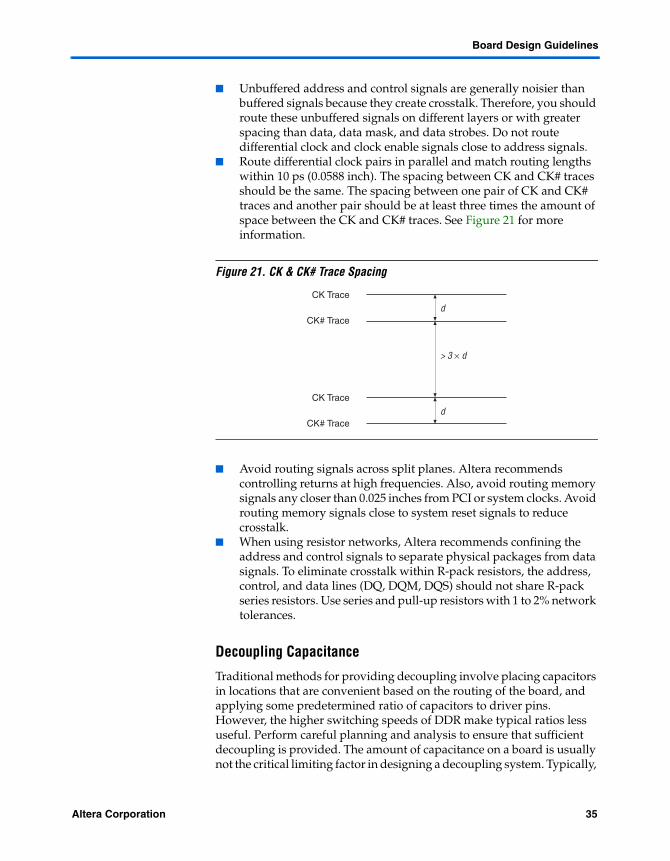
Route differential clock pairs in parallel and match routing lengths within 10 ps (0.0588 inch). The spacing between CK and CK# traces should be the same. The spacing between one pair of CK and CK# traces and another pair should be at least three times the amount of space between the CK and CK# traces. See Figure 21 for more information.
Figure 21. CK & CK# Trace Spacing
Avoid routing signals across split planes. Altera recommends controlling returns at high frequencies. Also, avoid routing memory signals any closer than 0.025 inches from PCI or system clocks. Avoid routing memory signals close to system reset signals to reduce crosstalk.
When using resistor networks, Altera recommends confining the address and control signals to separate physical packages from data signals. To eliminate crosstalk within R-pack resistors, the address, control, and data lines (DQ, DQM, DQS) should not share R-pack series resistors. Use series and pull-up resistors with 1 to 2% network tolerances.
Decoupling Capacitance
Traditional methods for providing decoupling involve placing capacitors in locations that are convenient based on the routing of the board, and applying some predetermined ratio of capacitors to driver pins. However, the higher switching speeds of DDR make typical ratios less useful. Perform careful planning and analysis to ensure that sufficient decoupling is provided. The amount of capacitance on a board is usually not the critical limiting factor in designing a decoupling system. Typically,
CK Trace
CK# Trace
CK Trace
CK# Trace
d
d
> 3 × d
Altera Corporation 35Preliminary

Interfacing DDR SDRAM with Cyclone Devices
the amount of inductance in the capacitor leads and the vias attaching the capacitors to the power and ground planes creates limitations. Altera recommends using 0.1-µF capacitors in an 0603-sized package to provide sufficient capacitance without adding too much inductance. Make VTT voltage decoupling on the motherboard close to the parallel pull-up resistors. Connect the decoupling capacitors between VTT and ground. The Cyclone memory interface board has a 0.1-µF capacitor for every other VTT pin. The Cyclone memory interface board also has 0.1- and 0.01-µF capacitors for every VDD and VDDQ pin.
Cyclone Memory Board
The Cyclone device family supports DDR SDRAM memory interfaces up to 133 MHz. The Cyclone memory board includes a Cyclone EP1C6Q240C6 device interfacing with a MT46V16M8 128-Mbyte DDR SDRAM device and a MT46V8M16 128-Mbyte DDR SDRAM device. Figure 22 shows the Cyclone memory board. The Cyclone device for this design board is configured to interface between two different DDR SDRAM devices. The 128-Mbyte DDR SDRAM device in the 2-Mbyte × 16-bit × 4-bank configuration verifies the DDR SDRAM operates correctly using dedicated DQS resources with an internally generated delay. The 128-Mbyte DDR SDRAM device in the 4-Mbyte × 8-bit × 4-bank configuration verifies the DDR SDRAM operates correctly using external trace delays. However, this memory device does not test whether DQS dedicated resources produce the DQS write strobes.
36 Altera CorporationPreliminary

Board Design Guidelines
Figure 22. Cyclone Memory Board
Figure 23 shows the Cyclone memory board block diagram. The board is powered by a 16-V DC power supply. The 16-V input is regulated down to various voltages to interface with the different peripherals. The board utilizes a National Semiconductor LM2676S-3.3 switching regulator to create the 3.3-V power rail from the 16-V external power supply. A Linear Technology LT1764AEQ-2.5 linear regulator creates 2.5-V power rails from the 3.3-V power rail. To power the Cyclone logic array voltage, a National Semiconductor LMS1587CS-1.5 linear regulator creates a 1.5-V power rail from the 3.3-V power rail. A National LP2995M DDR Termination Regulator generates the termination voltage (VTT) and reference voltage (VREF), as required by the SSTL-2 JEDEC standard. The LP2995M regulator has a current rating of 1.5 A with a load regulation of ±0.5%. The board design also has three separate power jacks so you can provide power to the power planes or rails from a bench supply.
Altera Corporation 37Preliminary

Interfacing DDR SDRAM with Cyclone Devices
Figure 23. Cyclone Board Block Diagram
You can input a user-generated clock through an SMA input to the Cyclone memory board, as well as use a 100-MHz surface mount oscillator (JITO-2-DS3AF-100.000). You can select between the sources using the select switch of the clock driver/multiplexer (ICS580-01) to the Cyclone device.
Cyclone EP1C6 FPGA240-pin PQFP
RS232Transceiver
DDR SDRAMMismatch
TracesOne Chip
Banks 1 and 3
ClockingCircuitry
10-Pin JTAGHeader
100-MilHeader
DDR SDRAMDQS
One ChipBanks 2 and 4
10-Pin ActiveSerial Header
EPCS4Active SerialConfiguration
Device
16-V PowerSupply
Connector,Banana Jacks,and Regulators
SerialPort
Four UserLEDs
Four UserPush Buttons
Two 7-SegmentLEDs
SystemLEDs
SystemPush ButtonTest Trace Input
SMA2
User DIPSwitches
Transceiver andReceiver
Transceiver andReceiver
CTS/RTS
CTS/RTS
16 Bits
Addressand Control
16 DQ Pins2 DQS Pins
8 DQ Pins1 DQS Pin
ASDO
DCLK, ASDI,CSn
Address andControl
38 Altera CorporationPreliminary

Board Design Guidelines
Cyclone Memory Board Characterization
Figure 24 shows the block diagram for the DDR SDRAM design used to test the Cyclone DDR interface. The design consists of DDR controller intellectual property (IP), linear feedback shift registers (LFSR), and user logic blocks. The DDR controller IP block consists of the Altera DDR SDRAM Controller IP MegaCore function. The linear feedback shift registers write data generator block generates random data to be written to the memory. The user logic block verifies if the read data is the same as the write data. The user LED will turn on if there are any errors.
Figure 24. Block Diagram of ×16 Interface DDR SDRAM Design
DDRMemory
Component
CLK
System Clock
ResetPass/Fail Flag
Write Clock
Data
Write Data [32..0]
SDRAM Clock
DQ[15..0]
DQS[1..0]
Command
ADDR[11..0]Read Data [32..0]
Cyclone Device
IP Block
DDR Controller
PLL
Linear FeedbackShift Register
Write DataGenerator
User Logic(Write, Read,
Compare)
Altera Corporation 39Preliminary

Interfacing DDR SDRAM with Cyclone Devices
Test Setup
The test setup used to characterize the Cyclone memory board is shown in Table 9.
Experimental Results
Table 10 lists the experimental results across different data width.
Conclusion Cyclone devices have dedicated circuitry to interface with up to 133-MHz DDR SDRAM with comfortable and consistent margin. Cyclone devices offer the memory interface that allows system designers to enhance their system performance through commercial off the shelf DRAM devices. By leveraging the continually decreasing cost of DRAM devices, system designers are able to keep their system design simple, reduce cost and improve performance.
Table 9. Test Setup for Cyclone Memory Board
Parameter Description
DDR controller IP Altera DDR SDRAM Controller MegaCore function
Memory Micron MT46V8M16TG-75 for x16 interface
Micron MT46V16M8TG-6T for ×8 interface
Data width 8- and 16-bit data bus
Cyclone device EP1C6Q240C6
Data transaction sequences Write all followed by read all
Termination Off-chip termination
Burst length 1, 2, or 4
Data pattern PRBS8
Operating conditions Bench test at room temperature
Table 10. Clock Frequency of Cyclone DDR Board
Data Width Clock Frequency (MHz)
×8 (1) 133
×16 (2) 133
Notes to Table 10:(1) ×8 interface uses an external trace delay to delay the DQS signal.(2) ×16 interface uses the internal programmable delay chain to delay the DQS signal.
40 Altera CorporationPreliminary

References
References JEDEC Standard Publication JESD79C, DDR SDRAM Specification, JEDEC Solid State Technology Association.
MT46V16M8TG/MT46V8M16TG, 128Mb: x8, x16 DDR SDRAM Data Sheet, Micron Technology, Inc.
DDR SDRAM Controller MegaCore Function User Guide, Altera Corporation
Revision History The information contained in version 1.1 of AN 348: Interfacing DDR SDRAM with Cyclone Devices supersedes information published in previous versions.
The following changes were made to AN 348: Interfacing DDR SDRAM with Cyclone Devices version 1.1:
Updated Figure 4. Added notes to Figure 5. Updated Figure 17.
Altera Corporation 41Preliminary

Interfacing DDR SDRAM with Cyclone Devices
42 Altera CorporationPreliminary
101 Innovation DriveSan Jose, CA 95134(408) 544-7000www.altera.comApplications Hotline:(800) 800-EPLDLiterature Services:[email protected]
Copyright © 2004 Altera Corporation. All rights reserved. Altera, The Programmable Solutions Company,the stylized Altera logo, specific device designations, and all other words and logos that are identified astrademarks and/or service marks are, unless noted otherwise, the trademarks and service marks of AlteraCorporation in the U.S. and other countries. All other product or service names are the property of their re-spective holders. Altera products are protected under numerous U.S. and foreign patents and pendingapplications, maskwork rights, and copyrights. Altera warrants performance of its semiconductor productsto current specifications in accordance with Altera's standard warranty, but reserves the right to make chang-es to any products and services at any time without notice. Altera assumes no responsibility or liabilityarising out of the application or use of any information, product, or service describedherein except as expressly agreed to in writing by Altera Corporation. Altera customersare advised to obtain the latest version of device specifications before relying on any pub-lished information and before placing orders for products or services.