Embed Size (px)
Citation preview
Altera Corporation AN-342-2.0
December 2005 ver. 2.0
Interfacing DDR SDRAM withStratix & Stratix GX Devices
Application Note 342
Introduction Traditionally, systems featuring FPGAs used single data rate (SDR) SDRAM, which transmits data on each rising edge of the clock signal. The total amount of data an SDR memory device can send or receive is equal to the clock speed multiplied by the bus width. To increase the data-rate transmission, one of those parameters must increase. With dual-edge clocking, double data rate (DDR) SDRAM can transmit data on both the rising and falling edge of the clock signal. DDR SDRAM effectively doubles the amount of data sent compared to SDR SDRAM without increasing the clock speed or the bus width.
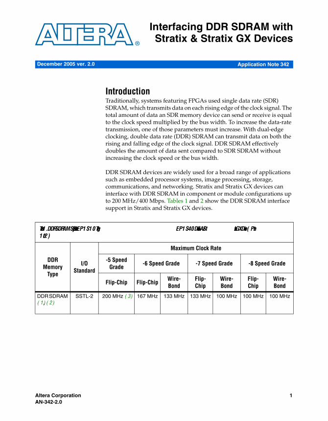
DDR SDRAM devices are widely used for a broad range of applications such as embedded processor systems, image processing, storage, communications, and networking. Stratix and Stratix GX devices can interface with DDR SDRAM in component or module configurations up to 200 MHz/400 Mbps. Tables 1 and 2 show the DDR SDRAM interface support in Stratix and Stratix GX devices.
Table 1. DDR SDRAM Support in Stratix EP1S10 Through EP1S40 Devices & All Stratix GX Devices (Part 1 of 2)
DDR Memory
Type
I/O Standard
Maximum Clock Rate
-5 Speed Grade -6 Speed Grade -7 Speed Grade -8 Speed Grade
Flip-Chip Flip-Chip Wire-Bond
Flip-Chip
Wire-Bond
Flip-Chip
Wire-Bond
DDR SDRAM (1), (2)
SSTL-2 200 MHz (3) 167 MHz 133 MHz 133 MHz 100 MHz 100 MHz 100 MHz
1Preliminary
Interfacing DDR SDRAM with Stratix & Stratix GX Devices
DDR SDRAM, side banks (2), (4)
SSTL-2 150 MHz 133 MHz 110 MHz 133 MHz 100 MHz 100 MHz 100 MHz
Notes to Table 1:(1) These maximum clock rates apply if the Stratix or Stratix GX device uses DQS phase-shift circuitry to interface with
DDR SDRAM. DQS phase-shift circuitry is only available in the top and bottom I/O banks (I/O banks 3, 4, 7, and 8).
(2) You should use the minimum drive strength setting in the Quartus II software for DDR SDRAM interfaces in Stratix and Stratix GX devices.
(3) To achieve 200 MHz interface speed, you should use loading of 10pF or less for Class II termination.(4) DDR SDRAM is supported on the Stratix device side banks (I/O banks 1, 2, 5, and 6) without dedicated DQS
phase-shift circuitry. The read DQS signal is ignored in this mode.
Table 1. DDR SDRAM Support in Stratix EP1S10 Through EP1S40 Devices & All Stratix GX Devices (Part 2 of 2)
DDR Memory
Type
I/O Standard
Maximum Clock Rate
-5 Speed Grade -6 Speed Grade -7 Speed Grade -8 Speed Grade
Flip-Chip Flip-Chip Wire-Bond
Flip-Chip
Wire-Bond
Flip-Chip
Wire-Bond
Table 2. DDR SDRAM Support in Stratix EP1S60 Through EP1S80 Devices
DDR Memory Type I/O Standard
Maximum Clock Rate
-5 Speed Grade -6 Speed Grade -7 Speed Grade
Flip-Chip Flip-Chip Flip-Chip
DDR SDRAM (1), (2) SSTL-2 167 MHz 167 MHz 133 MHz
DDR SDRAM, side banks (2), (3)
SSTL-2 150 MHz 133 MHz 133 MHz
Notes to Table 2:(1) These maximum clock rates apply if the Altera® Stratix or Stratix GX device uses DQS phase-shift circuitry to
interface with DDR SDRAM. DQS phase-shift circuitry is only available in the top and bottom I/O banks (I/O banks 3, 4, 7, and 8).
(2) You should use the minimum drive strength setting in the Quartus II software for DDR SDRAM interfaces in Stratix and Stratix GX devices.
(3) DDR SDRAM is supported on the Stratix device side banks (I/O banks 1, 2, 5, and 6) without dedicated DQS phase-shift circuitry. The read DQS signal is ignored in this mode.
2 Altera CorporationPreliminary
Functional Description
DDR SDRAM design requires both internal controller logic and a physical interface (often called the data path). Altera’s DDR SDRAM Controller MegaCore® function provides both the core and physical interface portions. You should always ensure your system is designed using the physical interface packaged with the IP Controller even if you will be designing your own core logic. This enables you to use the same physical interface that was tested by Altera and proven as robust. The MegaCore function gives you open source code for the data path and DQS postamble logic in addition to handling the timing analysis for the system, resynchronization, and DQS postamble logic timings. With the Altera DDR SDRAM Controller MegaCore function, you can easily generate a design that can be tested on the board using OpenCore® Plus hardware evaluation in minutes. You can then replace the encrypted part of the MegaCore function with your own DDR SDRAM state machine controller should you wish to do so.
This application note describes the DDR SDRAM interfacing in Stratix and Stratix GX devices. It also describes the timing analysis for the DDR SDRAM interface with Stratix and Stratix GX devices.
Functional Description
DDR SDRAM is a 2n-prefetch architecture with two data transfers per clock cycle. It uses a strobe, DQS, that is associated with a group of data pins (DQ) for read and write operations. Both the DQS and DQ ports are bidirectional. Address ports are shared for read and write operations.
Write and read operations are sent in bursts, and DDR SDRAM supports burst lengths of two, four, and eight. You provide two, four, or eight groups of data for each write transaction and receive two, four, or eight groups of data for each read transaction. The interval between when the read command is clocked into memory and the data is presented at the memory pins is called the column address strobe (CAS) latency. DDR SDRAM supports CAS latencies of 2, 2.5, and 3, depending on the operating frequency. Both the burst length and CAS latency are set in the DDR SDRAM mode register.
DDR SDRAM devices use the SSTL-2 class II I/O standard and can hold between 64 Mb to 1 Gb of data, according to the JEDEC specification. Each device is divided into four banks, and each bank has a fixed number of rows and columns. Only one row per bank can be accessed at one time. The ACTIVE command opens a row, and the PRECHARGE command closes a row.
For data reads, a delay-locked loop (DLL) inside the DDR SDRAM edge-aligns the DQ and DQS signals with respect to CK. The DLL must be turned on for normal operation, but can be turned off to save power or for debugging purposes. (All timing analyses in this document assume that
Altera Corporation 3Preliminary
Interfacing DDR SDRAM with Stratix & Stratix GX Devices
the DLL is on.) DDR SDRAM also has adjustable output drive strength. Altera recommends using a minimum drive strength setting on Altera devices.
f For more information on DDR SDRAM specifications, go to www.jedec.org.
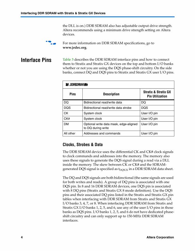
Interface Pins Table 3 describes the DDR SDRAM interface pins and how to connect them to Stratix and Stratix GX devices on the top and bottom I/O banks whether or not you are using the DQS phase-shift circuitry. On the side banks, connect DQ and DQS pins to Stratix and Stratix GX user I/O pins.
Clocks, Strobes & Data
The DDR SDRAM device uses the differential CK and CK# clock signals to clock commands and addresses into the memory. The memory also uses these signals to generate the DQS signal during a read via a DLL inside the memory. The skew between CK or CK# and the SDRAM-generated DQS signal is specified as tDQSCK in a DDR SDRAM data sheet.
The DQ and DQS signals are both bidirectional (the same signals are used for both writes and reads). A group of DQ pins is associated with one DQS pin. In 8 and 16 DDR SDRAM devices, one DQS pin is associated with 8 DQ pins (Stratix and Stratix GX 8 mode definition). Use the DQS pins and their associated DQ pins listed in the Stratix and Stratix GX pin tables when interfacing with DDR SDRAM from Stratix and Stratix GX I/O banks 3, 4, 7, or 8. When interfacing DDR SDRAM from Stratix and Stratix GX I/O banks 1, 2, 5, and 6, use any of the user I/O pins in those banks as DQS pins. I/O banks 1, 2, 5, and 6 do not have dedicated phase-shift circuitry and can only support up to 150-MHz DDR SDRAM interfaces.
Table 3. DDR SDRAM Interface Pins
Pins Description Stratix & Stratix GX Pin Utilization
DQ Bidirectional read/write data DQ
DQS Bidirectional read/write data strobe DQS
CK System clock User I/O pin
CK# System clock User I/O pin
DM Optional write data mask, edge-aligned to DQ during write
User I/O pin
All other Addresses and commands User I/O pin
4 Altera CorporationPreliminary
Interface Pins
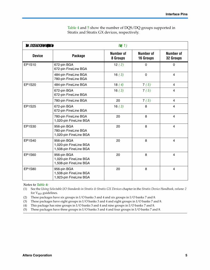
Table 4 and 5 show the number of DQS/DQ groups supported in Stratix and Stratix GX devices, respectively.
Table 4. DQS & DQ Bus Mode Support in Stratix Devices Note (1)
Device Package Number of 8 Groups
Number of16 Groups
Number of32 Groups
EP1S10 672-pin BGA672-pin FineLine BGA
12 (2) 0 0
484-pin FineLine BGA780-pin FineLine BGA
16 (3) 0 4
EP1S20 484-pin FineLine BGA 18 (4) 7 (5) 4
672-pin BGA672-pin FineLine BGA
16 (3) 7 (5) 4
780-pin FineLine BGA 20 7 (5) 4
EP1S25 672-pin BGA672-pin FineLine BGA
16 (3) 8 4
780-pin FineLine BGA1,020-pin FineLine BGA
20 8 4
EP1S30 956-pin BGA780-pin FineLine BGA1,020-pin FineLine BGA
20 8 4
EP1S40 956-pin BGA1,020-pin FineLine BGA1,508-pin FineLine BGA
20 8 4
EP1S60 956-pin BGA1,020-pin FineLine BGA1,508-pin FineLine BGA
20 8 4
EP1S80 956-pin BGA1,508-pin FineLine BGA1,923-pin FineLine BGA
20 8 4
Notes to Table 4:(1) See the Using Selectable I/O Standards in Stratix & Stratix GX Devices chapter in the Stratix Device Handbook, volume 2
for VREF guidelines.(2) These packages have six groups in I/O banks 3 and 4 and six groups in I/O banks 7 and 8.(3) These packages have eight groups in I/O banks 3 and 4 and eight groups in I/O banks 7 and 8.(4) This package has nine groups in I/O banks 3 and 4 and nine groups in I/O banks 7 and 8.(5) These packages have three groups in I/O banks 3 and 4 and four groups in I/O banks 7 and 8.
Altera Corporation 5Preliminary
Interfacing DDR SDRAM with Stratix & Stratix GX Devices
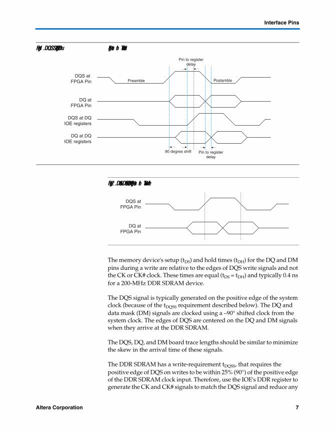
The data signals (DQ) are edge-aligned with the DQS signal during a read from the memory and center-aligned with the DQS signal during a write to the memory. The memory controller shifts the DQS signal during a write to center-align the DQ and DQS signals, and shifts the DQS signal during a read so that the DQ and DQS signals are center-aligned at the capture register. Stratix and Stratix GX devices use a phase-locked loop (PLL) to center-align the DQS signal with respect to the DQ signals during writes, and use dedicated DQS phase-shift circuitry to shift the incoming DQS signal during reads. Figure 1 shows an example where the DQS signal is center-aligned during a burst-of-two read. Figure 2 shows an example of the relationship between the data and the data strobe during a burst-of-two write.
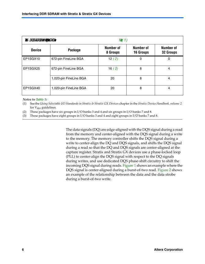
Table 5. DQS & DQ Bus Mode Support in Stratix GX Devices Note (1)
Device Package Number of8 Groups
Number of16 Groups
Number of32 Groups
EP1SGX10 672-pin FineLine BGA 12 (2) 0 0
EP1SGX25 672-pin FineLine BGA 16 (3) 8 4
1,020-pin FineLine BGA 20 8 4
EP1SGX40 1,020-pin FineLine BGA 20 8 4
Notes to Table 5:(1) See the Using Selectable I/O Standards in Stratix & Stratix GX Devices chapter in the Stratix Device Handbook, volume 2
for VREF guidelines.(2) These packages have six groups in I/O banks 3 and 4 and six groups in I/O banks 7 and 8.(3) These packages have eight groups in I/O banks 3 and 4 and eight groups in I/O banks 7 and 8.
6 Altera CorporationPreliminary
Interface Pins
Figure 1. DQS Signal Shift During Burst-of-Two Read
Figure 2. Data & Data Strobe During Burst-of-Two Write
The memory device’s setup (tDS) and hold times (tDH) for the DQ and DM pins during a write are relative to the edges of DQS write signals and not the CK or CK# clock. These times are equal (tDS = tDH) and typically 0.4 ns for a 200-MHz DDR SDRAM device.
The DQS signal is typically generated on the positive edge of the system clock (because of the tDQSS requirement described below). The DQ and data mask (DM) signals are clocked using a –90° shifted clock from the system clock. The edges of DQS are centered on the DQ and DM signals when they arrive at the DDR SDRAM.
The DQS, DQ, and DM board trace lengths should be similar to minimize the skew in the arrival time of these signals.
The DDR SDRAM has a write-requirement tDQSS, that requires the positive edge of DQS on writes to be within 25% (90°) of the positive edge of the DDR SDRAM clock input. Therefore, use the IOE’s DDR register to generate the CK and CK# signals to match the DQS signal and reduce any
DQS at DQIOE registers
DQS at FPGA Pin
DQ at DQIOE registers
DQ atFPGA Pin
Pin to registerdelay
Pin to registerdelay
90 degree shift
Preamble Postamble
DQS atFPGA Pin
DQ atFPGA Pin
Altera Corporation 7Preliminary
Interfacing DDR SDRAM with Stratix & Stratix GX Devices
process, voltage, and temperature variations.
To improve resynchronization for the 200-MHz DDR SDRAM interfaces, route the CK signal from the memory pin back to the Stratix or Stratix GX device. You can also use a separate output pin for the feedback clock. See “Read-Side Implementation Using the DQS Phase-Shift Circuitry” on page 9 for resynchronization details.
DM & Optional ECC Pins
The DDR SDRAM uses the data mask (DM) pins during a write. Driving the DM pins low marks that the write is valid. The memory masks the DQ signals if the DM pins are driven high. You can use any of the I/O pins in the same bank as the associated DQS/DQ pins to generate the DM signal.
The DM timing requirements at the DDR SDRAM input are identical to those for DQ data. The DDR registers, clocked by the –90° shifted clock, create the DM signals.
Some DDR SDRAM devices support error correction coding (ECC) to detect and automatically correct errors in data transmission. 72-bit DDR SDRAM modules contain 8 ECC pins in addition to 64 data pins. Connect the DDR ECC pins to a Stratix or Stratix GX device’s DQS/DQ group. The controller requires extra logic to encode and decode the ECC data.
Commands & Addresses
Commands and addresses in DDR SDRAM devices are clocked into the memory using the CK and CK# signals at single data rate using only one clock edge. DDR SDRAM devices have 12 to 14 address pins, depending on the device capacity. The address pins are multiplexed, so two clock cycles are required to send the row, column, and bank addresses. The CS, RAS, CAS, and WE pins are DDR SDRAM command pins.
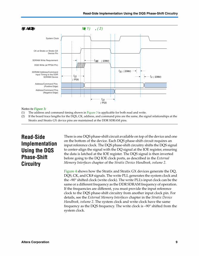
The DDR SDRAM address and command inputs require the same setup and hold times with respect to the DDR SDRAM clock. The Stratix and Stratix GX device’s address and command signals change at the same time as the DQS write signal because they are both generated from the system clock. The positive edge of the DDR SDRAM clock, CK, is aligned with DQS to satisfy tDQSS. If the command and address outputs are generated on the clock’s positive edge, they may not meet the hold time requirements (Figure 3). Therefore, you should use the negative edge of the system clock for the commands and addresses to the DDR SDRAM. You can use any of the I/O pins for the commands and addresses.
Figure 3 shows the address and command timing and the DDR SDRAM tDQSS, tDS, and tDH timing requirements.
8 Altera CorporationPreliminary
Read-Side Implementation Using the DQS Phase-Shift Circuitry
Figure 3. Address & Command Timing Notes (1), (2)
Notes to Figure 3:(1) The address and command timing shown in Figure 3 is applicable for both read and write.(2) If the board trace lengths for the DQS, CK, address, and command pins are the same, the signal relationships at the
Stratix and Stratix GX device pins are maintained at the DDR SDRAM pins.
Read-Side Implementation Using the DQS Phase-Shift Circuitry
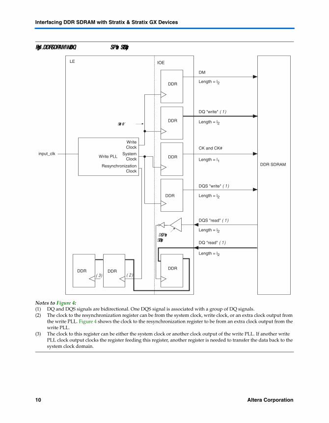
There is one DQS phase-shift circuit available on top of the device and one on the bottom of the device. Each DQS phase-shift circuit requires an input reference clock. The DQS phase-shift circuitry shifts the DQS signal to center-align the signal with the DQ signal at the IOE register, ensuring the data is latched at the IOE register. The DQS signal is then inverted before going to the DQ IOE clock ports, as described in the External Memory Interfaces chapter of the Stratix Device Handbook, volume 2.
Figure 4 shows how the Stratix and Stratix GX devices generate the DQ, DQS, CK, and CK# signals. The write PLL generates the system clock and the –90° shifted clock (write clock). The write PLL’s input clock can be the same or a different frequency as the DDR SDRAM frequency of operation. If the frequencies are different, you must provide the input reference clock to the DQS phase-shift circuitry from another input clock pin. For details, see the External Memory Interfaces chapter in the Stratix Device Handbook, volume 2. The system clock and write clock have the same frequency as the DQS frequency. The write clock is –90° shifted from the system clock.
System Clock
CK at Stratix or Stratix GXDevice Pin
DQS Write (at FPGA Pin)
Address/Command Pins (Positive Edge)
Address/Command Pins(Negative Edge)
SDRAM Write Requirement
SDRAM Address/CommandInput Timing to the DDR
SDRAM Device tCO
tCO
tH
(SDRAM)
(SDRAM)(FPGA)
(FPGA)
tSU
tDQSS (SDRAM)
Altera Corporation 9Preliminary
Interfacing DDR SDRAM with Stratix & Stratix GX Devices
Figure 4. DDR SDRAM With DQS Phase-Shift Circuitry
Notes to Figure 4:(1) DQ and DQS signals are bidirectional. One DQS signal is associated with a group of DQ signals.(2) The clock to the resynchronization register can be from the system clock, write clock, or an extra clock output from
the write PLL. Figure 4 shows the clock to the resynchronization register to be from an extra clock output from the write PLL.
(3) The clock to this register can be either the system clock or another clock output of the write PLL. If another write PLL clock output clocks the register feeding this register, another register is needed to transfer the data back to the system clock domain.
Write PLL
DDR
DDR
DDR
CK and CK#
DQS "read" (1)
DQ "read" (1)
IOELE
input_clk
DQ "write" (1)
Length = l2
Length = l2
Length = l1
Length = l2
DQS "write" (1)
Length = l2
Length = l2
DDR
DDR
DDRDDR
DQS Phase-Shift Circuitry
(2)(3)
SystemClock
ResynchronizationClock
WriteClock
DM
DDR SDRAM
Shifted -90˚
10 Altera CorporationPreliminary
Read-Side Implementation Using the DQS Phase-Shift Circuitry
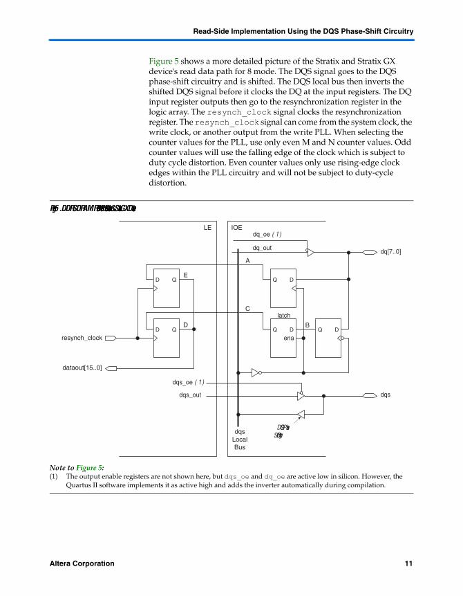
Figure 5 shows a more detailed picture of the Stratix and Stratix GX device’s read data path for 8 mode. The DQS signal goes to the DQS phase-shift circuitry and is shifted. The DQS local bus then inverts the shifted DQS signal before it clocks the DQ at the input registers. The DQ input register outputs then go to the resynchronization register in the logic array. The resynch_clock signal clocks the resynchronization register. The resynch_clock signal can come from the system clock, the write clock, or another output from the write PLL. When selecting the counter values for the PLL, use only even M and N counter values. Odd counter values will use the falling edge of the clock which is subject to duty cycle distortion. Even counter values only use rising-edge clock edges within the PLL circuitry and will not be subject to duty-cycle distortion.
Figure 5. DDR SDRAM Read Data Path in Stratix & Stratix GX Devices
Note to Figure 5:(1) The output enable registers are not shown here, but dqs_oe and dq_oe are active low in silicon. However, the
Quartus II software implements it as active high and adds the inverter automatically during compilation.
dqs_oe (1)
dq_oe (1)
dqs_out
dq_out
D Q
D Q
DQ
DQ DQ
LE IOE
ena
latch
dq[7..0]
dqs
DQS PhaseShift Circuitrydqs
LocalBus
B
A
C
D
E
resynch_clock
dataout[15..0]
Altera Corporation 11Preliminary
Interfacing DDR SDRAM with Stratix & Stratix GX Devices
DQS Phase-Shift Circuitry Use in DDR SDRAM Interfaces
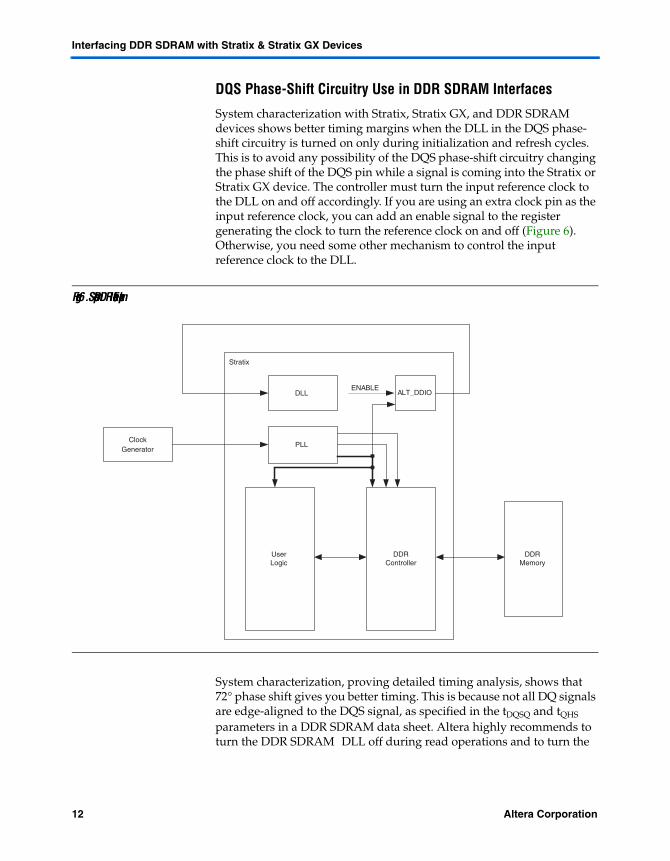
System characterization with Stratix, Stratix GX, and DDR SDRAM devices shows better timing margins when the DLL in the DQS phase-shift circuitry is turned on only during initialization and refresh cycles. This is to avoid any possibility of the DQS phase-shift circuitry changing the phase shift of the DQS pin while a signal is coming into the Stratix or Stratix GX device. The controller must turn the input reference clock to the DLL on and off accordingly. If you are using an extra clock pin as the input reference clock, you can add an enable signal to the register generating the clock to turn the reference clock on and off (Figure 6). Otherwise, you need some other mechanism to control the input reference clock to the DLL.
Figure 6. Simple DDR Interface Example
System characterization, proving detailed timing analysis, shows that 72° phase shift gives you better timing. This is because not all DQ signals are edge-aligned to the DQS signal, as specified in the tDQSQ and tQHS parameters in a DDR SDRAM data sheet. Altera highly recommends to turn the DDR SDRAM DLL off during read operations and to turn the
DDRController
UserLogic
DLL
PLLClock
Generator
Stratix
ALT_DDIOENABLE
DDRMemory
12 Altera CorporationPreliminary
Read-Side Implementation Using the DQS Phase-Shift Circuitry
DLL on during initialization and refresh cycles only. See Table 7 on page 19 for the detailed timing analysis for the DDR SDRAM read operation.
DQS Postamble
The DDR SDRAM DQ and DQS pins use the SSTL-2 class II I/O standard. If the Stratix, Stratix GX, or DDR SDRAM device do not drive the DQ and DQS pins, the signals go to a high-impedance state. Because a pull-up resistor terminates both DQ and DQS to VTT (1.25 V), the effective voltage on the high-impedance line is 1.25 V. According to the JEDEC JESD 8-9 specification for SSTL-2 I/O standard, this is an indeterminate logic level, and the input buffer can interpret this as either a logic high or logic low. If there is any noise on the DQS line, the input buffer may interpret that noise as actual strobe edges. Therefore, when the DQS signal goes to a high-impedance state after a read postamble, you should disable the clock to the input registers so that erroneous data is not latched in and all the data from the memory is resynchronized properly.
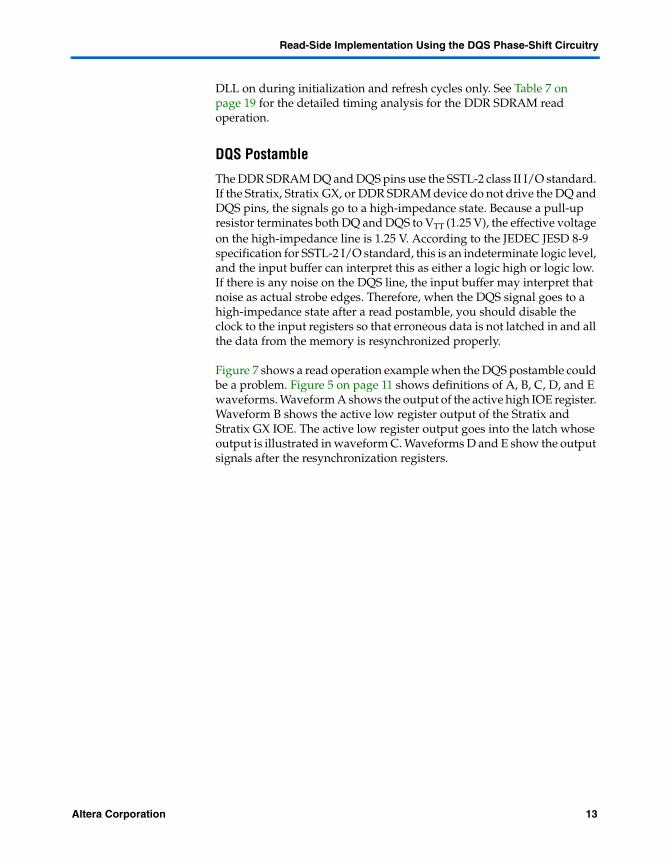
Figure 7 shows a read operation example when the DQS postamble could be a problem. Figure 5 on page 11 shows definitions of A, B, C, D, and E waveforms. Waveform A shows the output of the active high IOE register. Waveform B shows the active low register output of the Stratix and Stratix GX IOE. The active low register output goes into the latch whose output is illustrated in waveform C. Waveforms D and E show the output signals after the resynchronization registers.
Altera Corporation 13Preliminary
Interfacing DDR SDRAM with Stratix & Stratix GX Devices
Figure 7. Read Example With a DQS Postamble Issue
The first falling edge of the DQS at the IOE register occurs at 10 ns. At this point, data D0H is clocked in by the active low register (waveform B). At 12.5 ns, data D0L is sampled in by the active high register (waveform A) and data D0H passes through the latch (waveform C). In this example, the positive edge of the resynch_clock signal occurs at 16.5 ns, where both D0H and D0L are sampled by the LE’s resynchronization registers. Similarly, data D1H is clocked in by the active low register at 15 ns, data D1L is clocked in by the active high register, and data D1H passes through the latch at 17.5 ns. At 20 ns, noise on the DQS line causes a valid clock edge at the IOE registers that changes the values of waveforms A, B, and C. The next rising edge of the resynch_clock signal does not occur until 21.5 ns, but data D1L and D1H are not valid anymore at the output of the latch and the active-high input register. Therefore, the resynchronization registers do not sample D1L and D1H and may sample the wrong data instead.
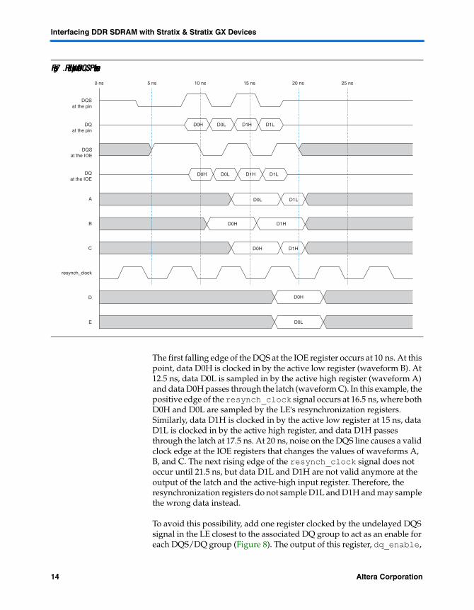
To avoid this possibility, add one register clocked by the undelayed DQS signal in the LE closest to the associated DQ group to act as an enable for each DQS/DQ group (Figure 8). The output of this register, dq_enable,
D0H D0L D1H
D0H
D0H
D0L
D1H
D1L
D0H D0L D1H D1L
D0L D1L
D0H D1H
DQSat the pin
DQSat the IOE
DQat the pin
DQat the IOE
A
B
C
resynch_clock
D
E
0 ns 5 ns 10 ns 15 ns 20 ns 25 ns
14 Altera CorporationPreliminary
Read-Side Implementation Using the DQS Phase-Shift Circuitry
controls clock enable for the DQ IOE registers. The data input to the LE register is set to GND, and the preset port of this register is connected to the dq_enable_preset signal. The controller should generate dq_enable_preset so that it is high when DQS is first detected low (during read preamble) and low during the cycle prior to the last active edge of DQS. This causes the dq_enable signal to go low with the last active negative edge of the DQS signal. Register AI and BI are then disabled before DQS goes into a high-impedance state. Latch CI has the last data captured by register BI, whether or not it is in the transparent or latched state.
Figure 8. Soft Logic to Avoid the DQS Postamble Issue
Notes to Figure 8:(1) Invert combout of the IOE for the DQS pin before feeding into inclock of the IOE for the DQ pin. This inversion
is automatic if you use an altdq megafunction for the DQ pins.(2) You can have 0, 1, or 2 LE buffers. These are required at lower frequencies to ensure that the capture registers are
not disabled too early.
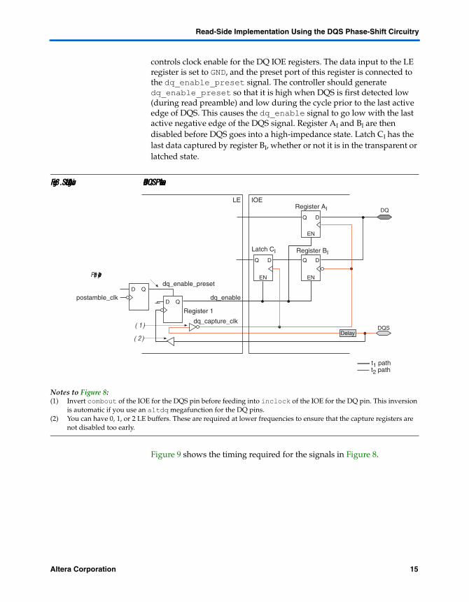
Figure 9 shows the timing required for the signals in Figure 8.
postamble_clk
t2 path t1 path
dq_capture_clk
dq_enable_preset
DQ
dq_enable
Preset (asynchronous)
(1)
(2)
D Q
D Q
Q D
Q D
DQSDelay
EN
Q D
EN
EN
Register AI
Register BI
Register 1
Latch CI
IOELE
Altera Corporation 15Preliminary
Interfacing DDR SDRAM with Stratix & Stratix GX Devices
Figure 9. DQS Postamble Workaround Soft Logic Timing Diagram
To analyze the timing of the circuit shown in Figure 8, assume that t1 is the delay from the DQS pad through the compensated delay to registers AI and BI, t2 is the delay from the DQS pad through register 1 (tCO) to the enable pin of registers AI and BI, and T is the clock period. The timing equations are then as follows:
t2 > t1 + micro hold timet2 < t1 + 0.4T – micro setup time
Because t1 is actually the 72° phase shift plus some PVT variation, t1a is the delay that varies with PVT so that t1 is either t1a + 0.2T so that the equations above are now as follows:
t2 > t1a + 0.2Tt2 < t1a + 0.2T + 0.4T
The equation can be rearranged to 0.2T < t2 – t1a < 0.6T
The equation above shows that t2 and t1a vary the same way with PVT, so when performing timing analysis, the maximum timing for t2 should be considered with the maximum timing for t1a, and vice versa for minimum timing. The equations in Table 6 show the timing requirements for a specific frequency of operation when using the 72° phase shifts, respectively:
Table 6. Timing Requirements Using 72° Phase Shift
Frequency Equation
200 MHz 1 ns < t2 – t1 a < 3 ns
166 MHz 1. 2 ns < t2 – t1 a < 3.6 ns
133 MHz 1.5 ns < t2 – t1 a < 4.5 ns
DQS
dq_enable
dq_enable_preset
16 Altera CorporationPreliminary
Read-Side Implementation Using the DQS Phase-Shift Circuitry
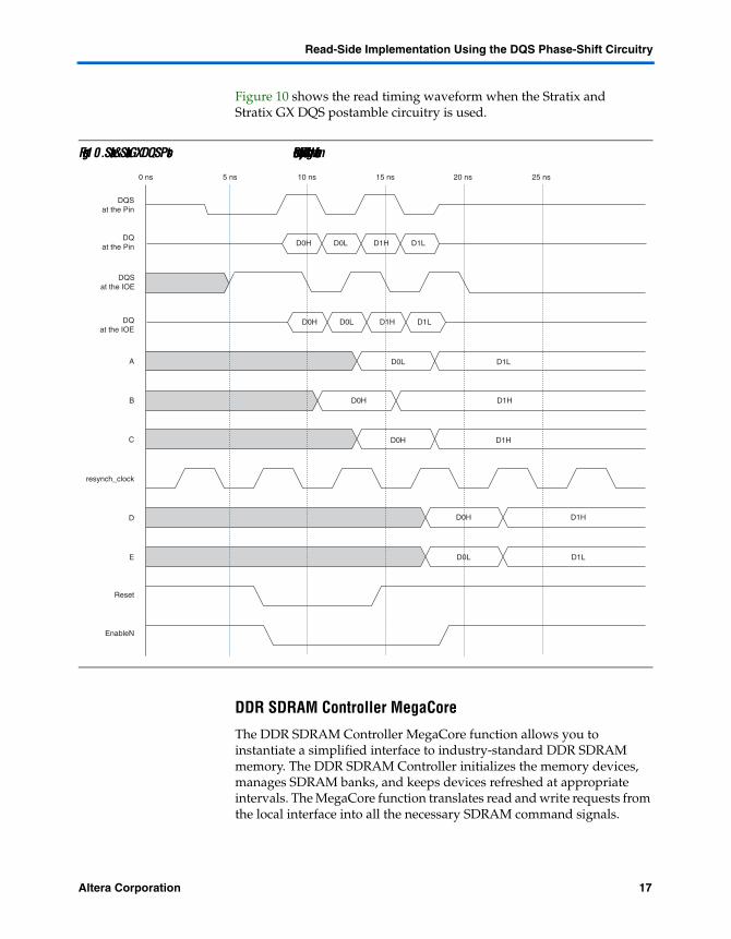
Figure 10 shows the read timing waveform when the Stratix and Stratix GX DQS postamble circuitry is used.
Figure 10. Stratix & Stratix GX DQS Postamble Circuitry Read Timing Waveform
DDR SDRAM Controller MegaCore
The DDR SDRAM Controller MegaCore function allows you to instantiate a simplified interface to industry-standard DDR SDRAM memory. The DDR SDRAM Controller initializes the memory devices, manages SDRAM banks, and keeps devices refreshed at appropriate intervals. The MegaCore function translates read and write requests from the local interface into all the necessary SDRAM command signals.
D0H
D0H
D0L
D1H
D1L
D1H
D0L D1L
D0H D1H
A
B
C
resynch_clock
D
E
Reset
EnableN
0 ns 5 ns 10 ns 15 ns 20 ns 25 ns
D0H D0L D1H D1L
D0H D0L D1H D1L
DQSat the Pin
DQSat the IOE
DQat the Pin
DQat the IOE
Altera Corporation 17Preliminary
Interfacing DDR SDRAM with Stratix & Stratix GX Devices
The DDR SDRAM Controller contains encrypted control logic as well as an open source data path that you can use in your design without a license. Download this MegaCore function (whether you plan to use the Altera DDR SDRAM controller or not) to get the open source data path, open source DQS postamble logic, placement constraints and timing margin analysis.
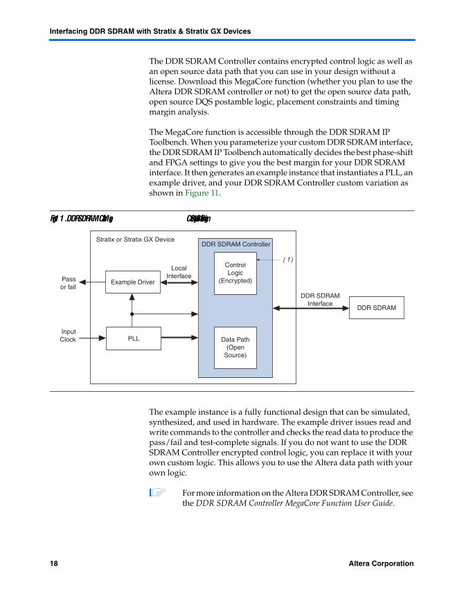
The MegaCore function is accessible through the DDR SDRAM IP Toolbench. When you parameterize your custom DDR SDRAM interface, the DDR SDRAM IP Toolbench automatically decides the best phase-shift and FPGA settings to give you the best margin for your DDR SDRAM interface. It then generates an example instance that instantiates a PLL, an example driver, and your DDR SDRAM Controller custom variation as shown in Figure 11.
Figure 11. DDR SDRAM Controller MegaCore System Level Block Diagram
The example instance is a fully functional design that can be simulated, synthesized, and used in hardware. The example driver issues read and write commands to the controller and checks the read data to produce the pass/fail and test-complete signals. If you do not want to use the DDR SDRAM Controller encrypted control logic, you can replace it with your own custom logic. This allows you to use the Altera data path with your own logic.
1 For more information on the Altera DDR SDRAM Controller, see the DDR SDRAM Controller MegaCore Function User Guide.
ControlLogic
(Encrypted)
Data Path(Open
Source)
DDR SDRAM
Example Driver
PLL
LocalInterface
DDR SDRAMInterface
DDR SDRAM Controller
Passor fail
InputClock
(1)
Stratix or Stratix GX Device
18 Altera CorporationPreliminary
Read-Side Implementation Using the DQS Phase-Shift Circuitry
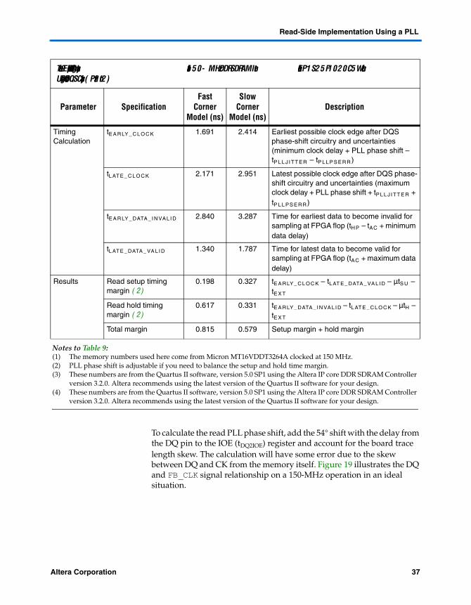
Read Timing Margin Analysis
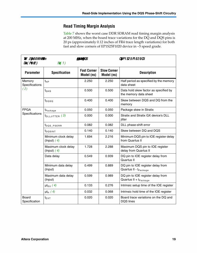
Table 7 shows the worst case DDR SDRAM read timing margin analysis at 200 MHz, when the board trace variations for the DQ and DQS pins is 20 ps (approximately 0.12 inches of FR4 trace length variations) for both fast and slow corners of EP1S25F1020 device in –5 speed grade.
Table 7. Example 200MHz Read Timing Analysis When Using DQS Circuitry in an EP1S25F1020C5 Device (Part 1 of 2) Note (1)
Parameter Specification Fast Corner Model (ns)
Slow Corner Model (ns) Description
Memory Specifications (2)
tH P 2.250 2.250 Half period as specified by the memory data sheet
tQ HS 0.500 0.500 Data hold skew factor as specified by the memory data sheet
tD QS Q 0.400 0.400 Skew between DQS and DQ from the memory
FPGA Specifications
tPa ck a g e 0.050 0.050 Package skew in Stratix
tD L L J I T T E R (3) 0.000 0.000 Stratix and Stratix GX device’s DLL jitter
tD QS _ P S E R R 0.082 0.082 DLL phase-shift error
tD QS I N T 0.140 0.140 Skew between DQ and DQS
Minimum clock delay (Input) (4)
1.694 2.216 Minimum DQS pin to IOE register delay from Quartus II
Maximum clock delay (Input) (4)
1.728 2.288 Maximum DQS pin to IOE register delay from Quartus II
Data delay 0.549 0.939 DQ pin to IOE register delay from Quartus II
Minimum data delay (Input)
0.499 0.889 DQ pin to IOE register delay from Quartus II - tPa ck a g e
Maximum data delay (Input)
0.599 0.989 DQ pin to IOE register delay from Quartus II + tPa ck a g e
µtS U (4) 0.133 0.276 Intrinsic setup time of the IOE register
µtH (4) 0.032 0.068 Intrinsic hold time of the IOE register
Board Specification
tE X T 0.020 0.020 Board trace variations on the DQ and DQS lines
Altera Corporation 19Preliminary
Interfacing DDR SDRAM with Stratix & Stratix GX Devices
Table 7 is divided into five sections: memory specifications, FPGA specifications, board specification, timing calculations, and results. The memory specifications section lists the items from a memory data sheet used in the calculation. The FPGA specifications section lists the items required for the calculation from the FPGA. The board specification section includes the board trace skew in the system. The timing calculations section shows the calculations, and the results section shows the final setup and hold-time margins.
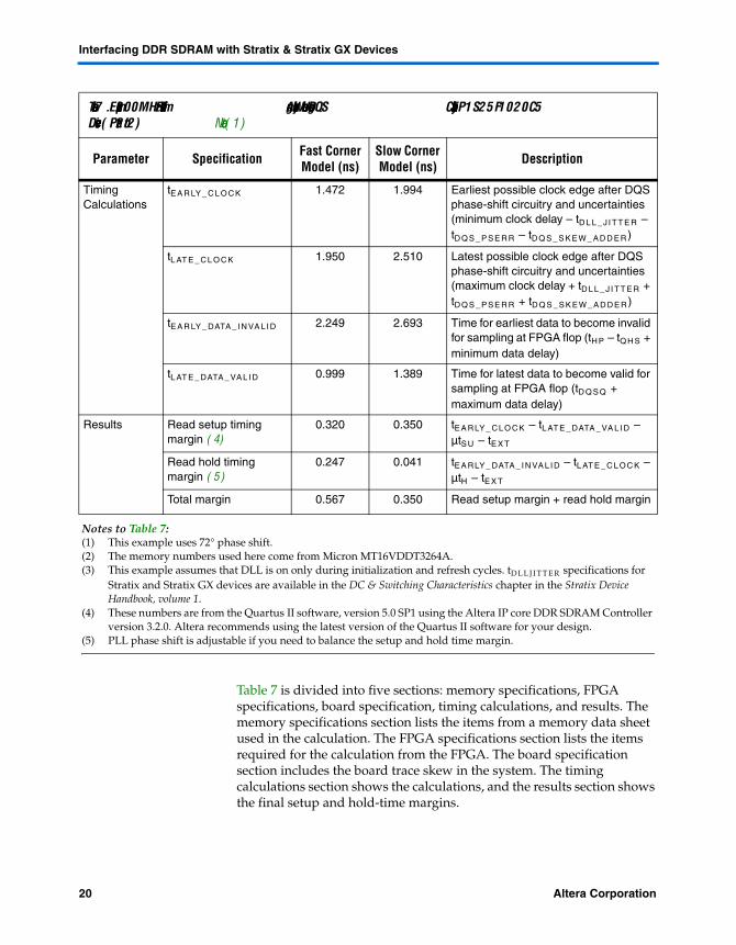
Timing Calculations
tE A R LY _ C L O CK 1.472 1.994 Earliest possible clock edge after DQS phase-shift circuitry and uncertainties (minimum clock delay – tD L L _ J I T T E R – tDQ S _ P S E R R – tDQ S _ S K E W _ A D D E R)
tL AT E _ CL O CK 1.950 2.510 Latest possible clock edge after DQS phase-shift circuitry and uncertainties (maximum clock delay + tD L L _ J I T T E R + tDQ S _ P S E R R + tD Q S _ S K E W _ A D DE R)
tE A R LY _ DATA _ I N VA L I D 2.249 2.693 Time for earliest data to become invalid for sampling at FPGA flop (tH P – tQ H S + minimum data delay)
tL AT E _ DATA _ VA L I D 0.999 1.389 Time for latest data to become valid for sampling at FPGA flop (tD Q S Q + maximum data delay)
Results Read setup timing margin (4)
0.320 0.350 tE A R LY _ C L O C K – tL AT E _ DATA _ VA L I D – µtS U – tE X T
Read hold timing margin (5)
0.247 0.041 tE A R LY _ DATA _ I N VA L I D – tL AT E _ C L O C K – µtH – tE X T
Total margin 0.567 0.350 Read setup margin + read hold margin
Notes to Table 7:(1) This example uses 72° phase shift. (2) The memory numbers used here come from Micron MT16VDDT3264A.(3) This example assumes that DLL is on only during initialization and refresh cycles. tD L L J I T T E R specifications for
Stratix and Stratix GX devices are available in the DC & Switching Characteristics chapter in the Stratix Device Handbook, volume 1.
(4) These numbers are from the Quartus II software, version 5.0 SP1 using the Altera IP core DDR SDRAM Controller version 3.2.0. Altera recommends using the latest version of the Quartus II software for your design.
(5) PLL phase shift is adjustable if you need to balance the setup and hold time margin.
Table 7. Example 200MHz Read Timing Analysis When Using DQS Circuitry in an EP1S25F1020C5 Device (Part 2 of 2) Note (1)
Parameter Specification Fast Corner Model (ns)
Slow Corner Model (ns) Description
20 Altera CorporationPreliminary
Read-Side Implementation Using the DQS Phase-Shift Circuitry
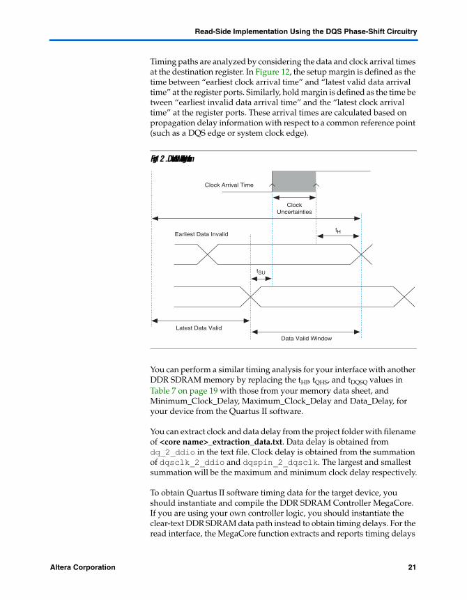
Timing paths are analyzed by considering the data and clock arrival times at the destination register. In Figure 12, the setup margin is defined as the time between “earliest clock arrival time” and “latest valid data arrival time” at the register ports. Similarly, hold margin is defined as the time be tween “earliest invalid data arrival time” and the “latest clock arrival time” at the register ports. These arrival times are calculated based on propagation delay information with respect to a common reference point (such as a DQS edge or system clock edge).
Figure 12. Data Valid Window Timing Waveform
You can perform a similar timing analysis for your interface with another DDR SDRAM memory by replacing the tHP, tQHS, and tDQSQ values in Table 7 on page 19 with those from your memory data sheet, and Minimum_Clock_Delay, Maximum_Clock_Delay and Data_Delay, for your device from the Quartus II software.
You can extract clock and data delay from the project folder with filename of <core name>_extraction_data.txt. Data delay is obtained from dq_2_ddio in the text file. Clock delay is obtained from the summation of dqsclk_2_ddio and dqspin_2_dqsclk. The largest and smallest summation will be the maximum and minimum clock delay respectively.
To obtain Quartus II software timing data for the target device, you should instantiate and compile the DDR SDRAM Controller MegaCore. If you are using your own controller logic, you should instantiate the clear-text DDR SDRAM data path instead to obtain timing delays. For the read interface, the MegaCore function extracts and reports timing delays
Clock Arrival Time
ClockUncertainties
Earliest Data Invalid
Latest Data Valid
Data Valid Window
tSU
tH
Altera Corporation 21Preliminary
Interfacing DDR SDRAM with Stratix & Stratix GX Devices
associated with each DQ and DQS pin in the <core_instance_name>extraction_data.txt file located in your project directory. Using this data file and the extract.tcl utility, minimum and maximum propagation delays on the clock and data path are extracted. This timing extraction is done twice, once with each device model (fast corner and slow corner). However, in Stratix and Stratix GX devices, there is only one data delay being extracted. This is because package skews are not modeled in Quartus II timing model for Stratix and Stratix GX devices.
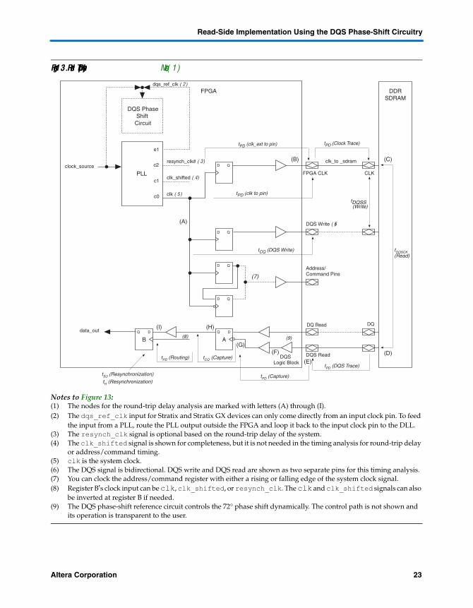
Round-Trip Delay Calculation
Read data is sent into the DDR registers using the DQS signal as a clock. Therefore, data must be transferred from the DQS clock domain to the system clock domain (resynchronization).
Figure 13 on page 23 shows the timing analysis and the round-trip delay in Stratix and Stratix GX devices. The round-trip delay is the delay from the FPGA clock to the DDR SDRAM and back to the FPGA (input to register B). You can calculate whether the register outputs clocked by the resynchronization clock need another resynchronization stage before getting to the system clock domain. This analysis is required to reliably transfer data from register A (in the IOE) to register B (in the LE).
1 You can also use a feedback clock and a second PLL for the resynchronization clock.
22 Altera CorporationPreliminary
Read-Side Implementation Using the DQS Phase-Shift Circuitry
Figure 13. Round-Trip Delay Note (1)
Notes to Figure 13:(1) The nodes for the round-trip delay analysis are marked with letters (A) through (I).(2) The dqs_ref_clk input for Stratix and Stratix GX devices can only come directly from an input clock pin. To feed
the input from a PLL, route the PLL output outside the FPGA and loop it back to the input clock pin to the DLL.(3) The resynch_clk signal is optional based on the round-trip delay of the system.(4) The clk_shifted signal is shown for completeness, but it is not needed in the timing analysis for round-trip delay
or address/command timing.(5) clk is the system clock.(6) The DQS signal is bidirectional. DQS write and DQS read are shown as two separate pins for this timing analysis.(7) You can clock the address/command register with either a rising or falling edge of the system clock signal.(8) Register B’s clock input can be clk, clk_shifted, or resynch_clk. The clk and clk_shifted signals can also
be inverted at register B if needed.(9) The DQS phase-shift reference circuit controls the 72° phase shift dynamically. The control path is not shown and
its operation is transparent to the user.
Q D
PLL
FPGA DDRSDRAM
DQS Read
data_out
(7)
clk (5)
clk_shifted (4)
resynch_clk# (3) clk_to _sdram
e1
tPD (DQS Trace)
c1
c2
c0
D Q
D Q
D Q
Q D
D Q
DQ Read
DQS Write (6)
Address/ Command Pins
clock_source
dqs_ref_clk (2)
DQS PhaseShift Circuit
DQ
CLKFPGA CLK
tCQ (Capture)tPD (Routing)
tSU (Resynchronization)
tH (Resynchronization)
(8)
tPD (Capture)
tPD (Clock Trace)
tDQSCK (Read)
tDQSS (Write)
tPD (clk to pin)
tPD (clk_ext to pin)
tCQ (DQS Write)
B A (9)
DQS Logic Block
(A)
(B) (C)
(D)
(E)
(F)(G)
(H)(I)
Altera Corporation 23Preliminary
Interfacing DDR SDRAM with Stratix & Stratix GX Devices
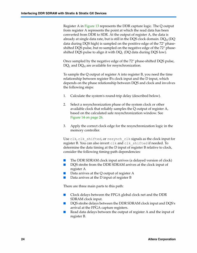
Register A in Figure 13 represents the DDR capture logic. The Q output from register A represents the point at which the read data has been converted from DDR to SDR. At the output of register A, the data is already at single data rate, but is still in the DQS clock domain. DQH (DQ data during DQS high) is sampled on the positive edge of the 72° phase-shifted DQS pulse, but re-sampled on the negative edge of the 72° phase-shifted DQS pulse to align it with DQL (DQ data during DQS low).
Once sampled by the negative edge of the 72° phase-shifted DQS pulse, DQL and DQH are available for resynchronization.
To sample the Q output of register A into register B, you need the time relationship between register B’s clock input and the D input, which depends on the phase relationship between DQS and clock and involves the following steps:
1. Calculate the system’s round-trip delay (described below).
2. Select a resynchronization phase of the system clock or other available clock that reliably samples the Q output of register A, based on the calculated safe resynchronization window. See Figure 14 on page 26.
3. Apply the correct clock edge for the resynchronization logic in the memory controller.
Use clk, clk_shifted, or resynch_clk signals as the clock input for register B. You can also invert clk and clk_shifted if needed. To determine the data timing at the D input of register B relative to clock, consider the following timing-path dependencies:
■ The DDR SDRAM clock input arrives (a delayed version of clock)■ DQS strobe from the DDR SDRAM arrives at the clock input of
register A■ Data arrives at the Q output of register A■ Data arrives at the D input of register B
There are three main parts to this path:
■ Clock delays between the FPGA global clock net and the DDR SDRAM clock input.
■ DQS strobe delays between the DDR SDRAM clock input and DQS’s arrival at the FPGA capture registers.
■ Read data delays between the output of register A and the input of register B.
24 Altera CorporationPreliminary
Read-Side Implementation Using the DQS Phase-Shift Circuitry
To determine the point at which the data can be reliably resynchronized, calculate the minimum and maximum round-trip delay, and then determine what resynchronization logic to use for your system. Remember to take into account PVT variations.
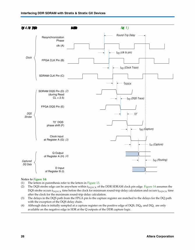
Figure 13 shows the individual delays between points (A) and (I). The sum of all these delays is the round-trip delay. Figure 14 shows the timing relationship of the signals for the delays between points (A) to (I) for a CAS latency of 2.5.
Altera Corporation 25Preliminary
Interfacing DDR SDRAM with Stratix & Stratix GX Devices
Figure 14. Round-Trip Delay Calculation Without a Feedback Clock Note (1)
Notes to Figure 14:(1) The letters in parenthesis refer to the letters in Figure 13.(2) The DQS strobe edge can be anywhere within tD Q S C K of the DDR SDRAM clock pin edge. Figure 14 assumes the
DQS strobe occurs tD Q S C K time before the clock for minimum round-trip delay calculation and occurs tD Q S C K time after the clock for the maximum round-trip delay calculation.
(3) The delays in the DQS path from the FPGA pin to the capture register are matched to the delays for the DQ path with the exception of the DQS delay chain.
(4) Although data is initially sampled at a capture register on the positive edge of DQS, DQH and DQL are only available on the negative edge in SDR at the Q outputs of the DDR capture logic.
clk (A)
Round-Trip Delay
tPD (clk to pin)
FPGA CLK Pin (B)
tPD (Clock Trace)
SDRAM CLK Pin (C)
tDQSCK
SDRAM DQS Pin (D)(during Read
CL = 2.5) tPD (DQS Trace)
tPD (Capture)
FPGA DQS Pin (E)
72˚
72˚ DQS phase shift (F)
Clock input at Register A (G)
tCQ (Capture)
Q Output of Register A (H)
tPD (Routing)
D Inputof Register B (I)
ResynchronizationPhase
Clock
DQSStrobe
CapturedDQ Data
(2)
(3)
(4)
26 Altera CorporationPreliminary
Read-Side Implementation Using the DQS Phase-Shift Circuitry
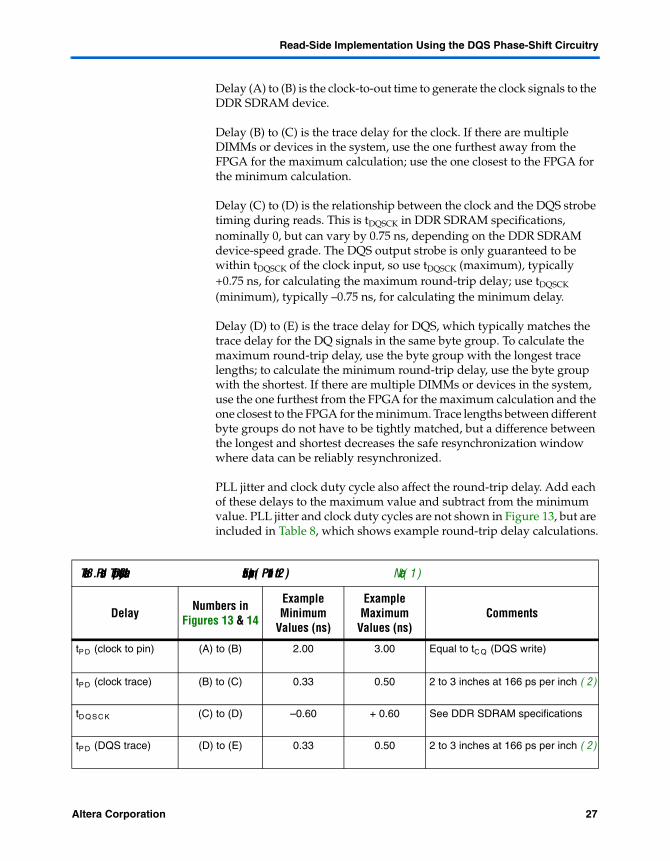
Delay (A) to (B) is the clock-to-out time to generate the clock signals to the DDR SDRAM device.
Delay (B) to (C) is the trace delay for the clock. If there are multiple DIMMs or devices in the system, use the one furthest away from the FPGA for the maximum calculation; use the one closest to the FPGA for the minimum calculation.
Delay (C) to (D) is the relationship between the clock and the DQS strobe timing during reads. This is tDQSCK in DDR SDRAM specifications, nominally 0, but can vary by 0.75 ns, depending on the DDR SDRAM device-speed grade. The DQS output strobe is only guaranteed to be within tDQSCK of the clock input, so use tDQSCK (maximum), typically +0.75 ns, for calculating the maximum round-trip delay; use tDQSCK
(minimum), typically –0.75 ns, for calculating the minimum delay.
Delay (D) to (E) is the trace delay for DQS, which typically matches the trace delay for the DQ signals in the same byte group. To calculate the maximum round-trip delay, use the byte group with the longest trace lengths; to calculate the minimum round-trip delay, use the byte group with the shortest. If there are multiple DIMMs or devices in the system, use the one furthest from the FPGA for the maximum calculation and the one closest to the FPGA for the minimum. Trace lengths between different byte groups do not have to be tightly matched, but a difference between the longest and shortest decreases the safe resynchronization window where data can be reliably resynchronized.
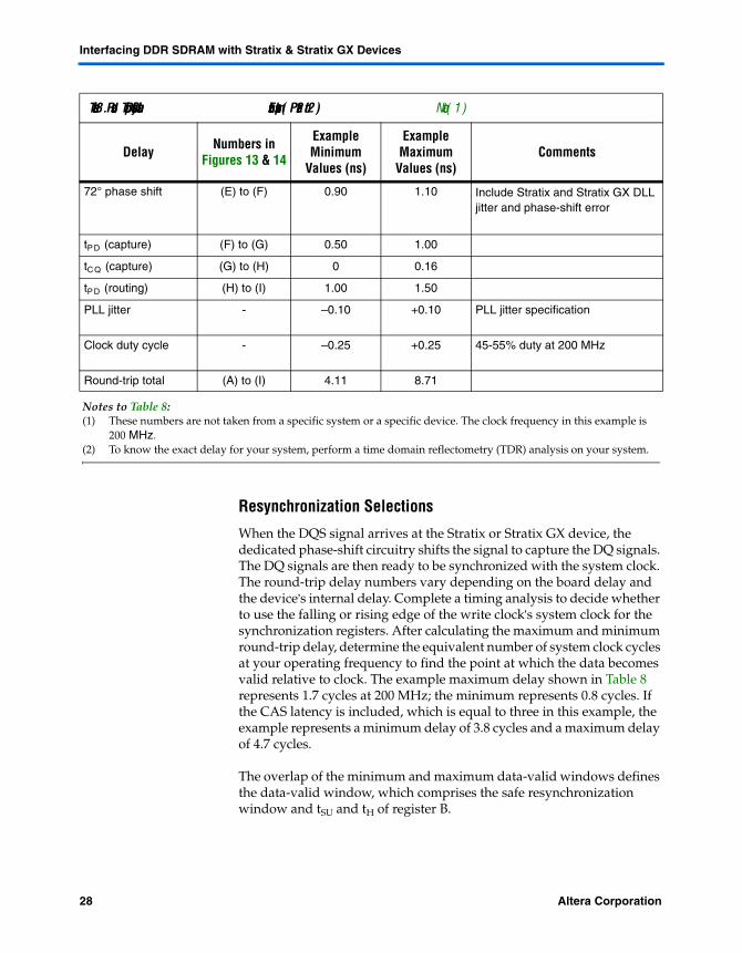
PLL jitter and clock duty cycle also affect the round-trip delay. Add each of these delays to the maximum value and subtract from the minimum value. PLL jitter and clock duty cycles are not shown in Figure 13, but are included in Table 8, which shows example round-trip delay calculations.
Table 8. Round-Trip Delay Calculation Example (Part 1 of 2) Note (1)
Delay Numbers in Figures 13 & 14
Example Minimum
Values (ns)
Example Maximum
Values (ns)Comments
tP D (clock to pin) (A) to (B) 2.00 3.00 Equal to tC Q (DQS write)
tP D (clock trace) (B) to (C) 0.33 0.50 2 to 3 inches at 166 ps per inch (2)
tD Q S C K (C) to (D) –0.60 + 0.60 See DDR SDRAM specifications
tP D (DQS trace) (D) to (E) 0.33 0.50 2 to 3 inches at 166 ps per inch (2)
Altera Corporation 27Preliminary
Interfacing DDR SDRAM with Stratix & Stratix GX Devices
Resynchronization Selections
When the DQS signal arrives at the Stratix or Stratix GX device, the dedicated phase-shift circuitry shifts the signal to capture the DQ signals. The DQ signals are then ready to be synchronized with the system clock. The round-trip delay numbers vary depending on the board delay and the device’s internal delay. Complete a timing analysis to decide whether to use the falling or rising edge of the write clock’s system clock for the synchronization registers. After calculating the maximum and minimum round-trip delay, determine the equivalent number of system clock cycles at your operating frequency to find the point at which the data becomes valid relative to clock. The example maximum delay shown in Table 8 represents 1.7 cycles at 200 MHz; the minimum represents 0.8 cycles. If the CAS latency is included, which is equal to three in this example, the example represents a minimum delay of 3.8 cycles and a maximum delay of 4.7 cycles.
The overlap of the minimum and maximum data-valid windows defines the data-valid window, which comprises the safe resynchronization window and tSU and tH of register B.
72° phase shift (E) to (F) 0.90 1.10 Include Stratix and Stratix GX DLL jitter and phase-shift error
tP D (capture) (F) to (G) 0.50 1.00
tC Q (capture) (G) to (H) 0 0.16
tP D (routing) (H) to (I) 1.00 1.50
PLL jitter - –0.10 +0.10 PLL jitter specification
Clock duty cycle - –0.25 +0.25 45-55% duty at 200 MHz
Round-trip total (A) to (I) 4.11 8.71
Notes to Table 8:(1) These numbers are not taken from a specific system or a specific device. The clock frequency in this example is
200 MHz. (2) To know the exact delay for your system, perform a time domain reflectometry (TDR) analysis on your system.
Table 8. Round-Trip Delay Calculation Example (Part 2 of 2) Note (1)
Delay Numbers in Figures 13 & 14
Example Minimum
Values (ns)
Example Maximum
Values (ns)Comments
28 Altera CorporationPreliminary
Read-Side Implementation Using the DQS Phase-Shift Circuitry
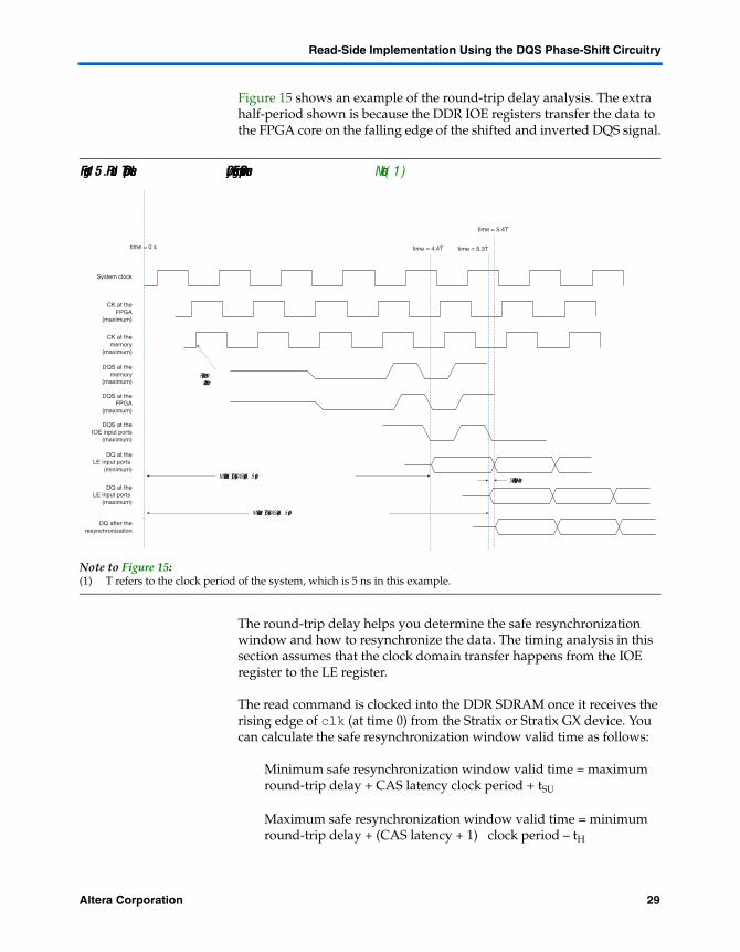
Figure 15 shows an example of the round-trip delay analysis. The extra half-period shown is because the DDR IOE registers transfer the data to the FPGA core on the falling edge of the shifted and inverted DQS signal.
Figure 15. Round-Trip Delay Diagram Example One Note (1)
Note to Figure 15:(1) T refers to the clock period of the system, which is 5 ns in this example.
The round-trip delay helps you determine the safe resynchronization window and how to resynchronize the data. The timing analysis in this section assumes that the clock domain transfer happens from the IOE register to the LE register.
The read command is clocked into the DDR SDRAM once it receives the rising edge of clk (at time 0) from the Stratix or Stratix GX device. You can calculate the safe resynchronization window valid time as follows:
Minimum safe resynchronization window valid time = maximum round-trip delay + CAS latency clock period + tSU
Maximum safe resynchronization window valid time = minimum round-trip delay + (CAS latency + 1) clock period – tH
System clock
CK at theFPGA
(maximum)
DQS at theFPGA
(maximum)
DQS at theIOE input ports
(maximum)
DQ at theLE input ports
(maximum)
DQ at theLE input ports
(minimum)
DQ after theresynchronization
CK at thememory
(maximum)
DQS at thememory
(maximum)
time = 0 s time = 4.4T time = 5.3T
time = 5.4T
Safe Resynchronization WindowMinimum Round-Trip Delay + CAS Latency + 0.5 period
Maximum Round-Trip Delay + CAS Latency + 0.5 period
Read CommandLatched Here
Altera Corporation 29Preliminary
Interfacing DDR SDRAM with Stratix & Stratix GX Devices
Table 8 on page 27 shows an example where the maximum round-trip delay is 8.71 ns (~1.7 clock cycle), and the minimum round-trip delay is 4.11 ns (~0.8 clock cycle). Plugging these numbers into the above minimum and maximum safe resynchronization window valid time equations, the example system shows the minimum safe resynchronization window valid time is 4.7 cycles and the maximum safe resynchronization window valid time is 4.8 cycles (with tSU and tH ignored).
The size of the safe resynchronization window in the example is then 0.1 cycle, calculated by the following equation:
Safe resynchronization window size = maximum safe resynchronization window valid time –minimum safe resynchronization window valid time
The size of your safe resynchronization window should be larger than 150 ps to accommodate worst case clock skew between two output clocks of the PLL of 150 ps.
After you calculate the safe resynchronization window time, determine how many half clock cycles elapse from time 0 to the minimum safe resynchronization window valid time (numcycle) by calculating the ceiling function of the minimum safe resynchronization window valid time divided by half a clock cycle. To find out whether the safe resynchronization window falls within a clock edge, multiply numcycle by half a clock cycle. If the result is less than the maximum safe resynchronization window valid time, a system clock edge falls within the safe resynchronization window. Otherwise you need an extra PLL output for your resynchronization clock.
The example in Table 8 on page 27, as depicted in Figure 15, shows that numcycle is equal to 10 and that the safe resynchronization window does not fall within a system clock edge.
If you do not need a resynchronization clock and numcycle is an even number, the active system clock edge for resynchronization is the positive edge. If numcycle is odd, the resynchronization system clock edge is the negative edge, and you must determine the resynchronization phase selection.
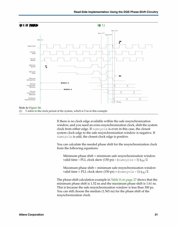
Figure 16 shows an example where the safe resynchronization window is within a system clock edge. In the example, numcycle is equal to 9 (time = 4.5T), and the negative edge of the system clock is used for the resynchronization clock.
30 Altera CorporationPreliminary
Read-Side Implementation Using the DQS Phase-Shift Circuitry
Figure 16. Round-Trip Delay Diagram Clock Example Two Note (1)
Note to Figure 16:(1) T refers to the clock period of the system, which is 5 ns in this example.
If there is no clock edge available within the safe resynchronization window, and you need an extra resynchronization clock, shift the system clock from either edge. If numcycle is even in this case, the closest system clock edge to the safe resynchronization window is negative. If numcycle is odd, the closest clock edge is positive.
You can calculate the needed phase shift for the resynchronization clock from the following equations:
Minimum phase shift = minimum safe resynchronization window valid time – PLL clock skew (150 ps) – (numcycle – 1) tCK/2
Maximum phase shift = minimum safe resynchronization window valid time + PLL clock skew (150 ps) + (numcycle – 1) tCK/2
The phase-shift calculation example in Table 8 on page 27 shows that the minimum phase shift is 1.52 ns and the maximum phase shift is 1.61 ns. This is because the safe resynchronization window is less than 300 ps. You can still choose the median (1.565 ns) for the phase shift of the resynchronization clock.
System Clock
CK at theFPGA
DQS at theFPGA
DQS at theIOE Input Ports
DQ at theLE Input Ports
(Maximum)
DQ after theResynchronization
DQ at theLE Input Ports
(Minimum)
CK at theMemory
DQS at theMemory
time = 0 s
time = 4.7T
time = 5.7T
time = 5.2T
Safe Resynchronization Window
LE µtco
Minimum Round-Trip Delay + CAS Latency + 0.5 period
Maximum Round-Trip Delay + CAS Latency + 0.5 period
Read CommandLatched Here
System Clock Edge to beused for Resynchronization-
Altera Corporation 31Preliminary
Interfacing DDR SDRAM with Stratix & Stratix GX Devices
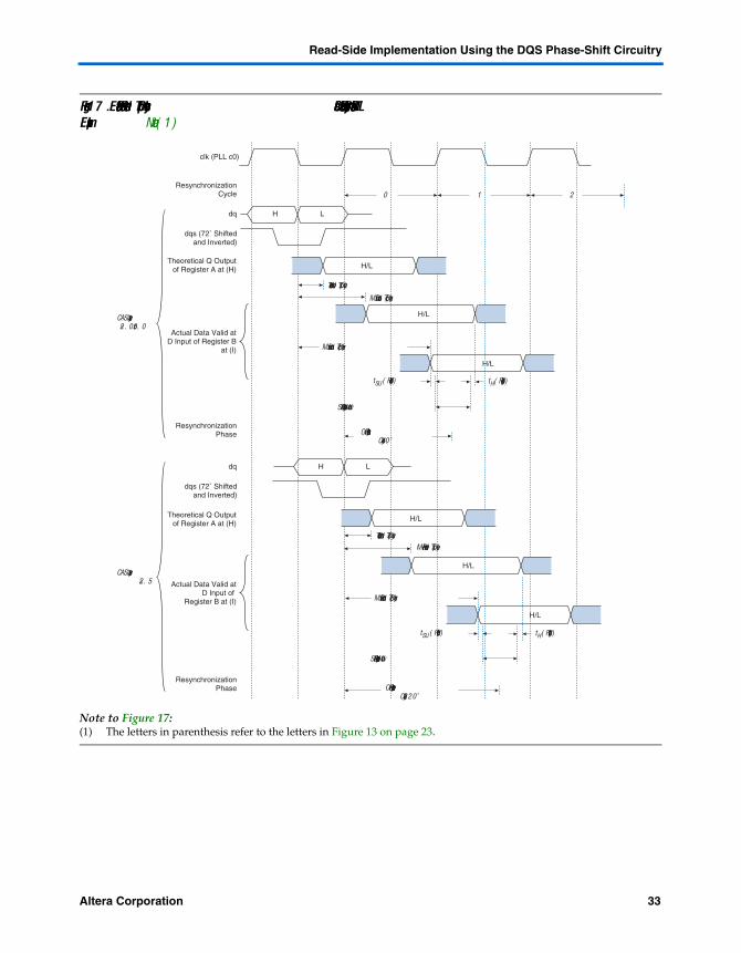
You then need to convert the results to the equivalent degree phase shifts. If the closest clock edge to the safe resynchronization window is negative, add or subtract 180° after the conversion to shift the clock from the positive edge. For the example in Table 8 on page 27, the phase-shift range is between 1.52 to 1.61 ns, based on the negative edge clock. The median of this number is 1.565 ns, which equates to ~113° (from 200-MHz clock). If you want to shift this clock from the positive edge of the system clock, use either 293° (113° + 180°) or – 67° (113° – 180°).
The Altera DDR SDRAM Controller MegaCore function allows you to set the resynchronization cycle and phase (Figure 17). The 0 resynchronization cycle starts at the first rising edge of the system clock (clk) after the DQS signal’s first falling edge at the IOE register. Each resynchronization cycle is one clock period. If there is no clock edge within the safe resynchronization window, you must set the phase shift. In the example shown in Figure 15 on page 29, you must choose the 0 resynchronization cycle with a 40° phase shift to set CAS latency to 2.0 or 3.0. Select the 0 resynchronization cycle with a 220° phase shift to set CAS latency to 2.5.
32 Altera CorporationPreliminary
Read-Side Implementation Using the DQS Phase-Shift Circuitry
Figure 17. Effect of Read Round-Trip Delay on the Choice of Resynchronization Phase for RTL Example Note (1)
Note to Figure 17: (1) The letters in parenthesis refer to the letters in Figure 13 on page 23.
clk (PLL c0)
H L
0 1 2
dq
CAS Latency= 2.5
dqs (72˚ Shiftedand Inverted)
Theoretical Q Output of Register A at (H)
Theoretical Q Output of Register A at (H)
Actual Data Valid atD Input of Register B
at (I)
ResynchronizationPhase
dq
CAS Latency= 2.0 or 3.0
dqs (72˚ Shiftedand Inverted)
ResynchronizationCycle
H/L
Minimum Round-Trip Delay
H/L
H/L
Theoretical Round-Trip Delay
Theoretical Round-Trip Delay
Maximum Round-Trip Delay
H/L
Actual Data Valid atD Input of
Register B at (I)
Minimum Round-Trip Delay
H/L
H/L
H L
Safe Resynchronization Window
tH (Register B)
One ResynchronizationCycle + 220˚
Safe Resynchronization Window
tSU (Register B)
ResynchronizationPhase One Resynchronization
Cycle + 40˚
Maximum Round-Trip Delay
tH (Register B)tSU (Register B)
Altera Corporation 33Preliminary
Interfacing DDR SDRAM with Stratix & Stratix GX Devices
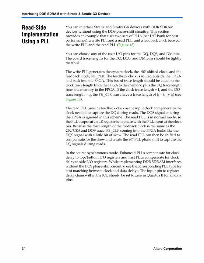
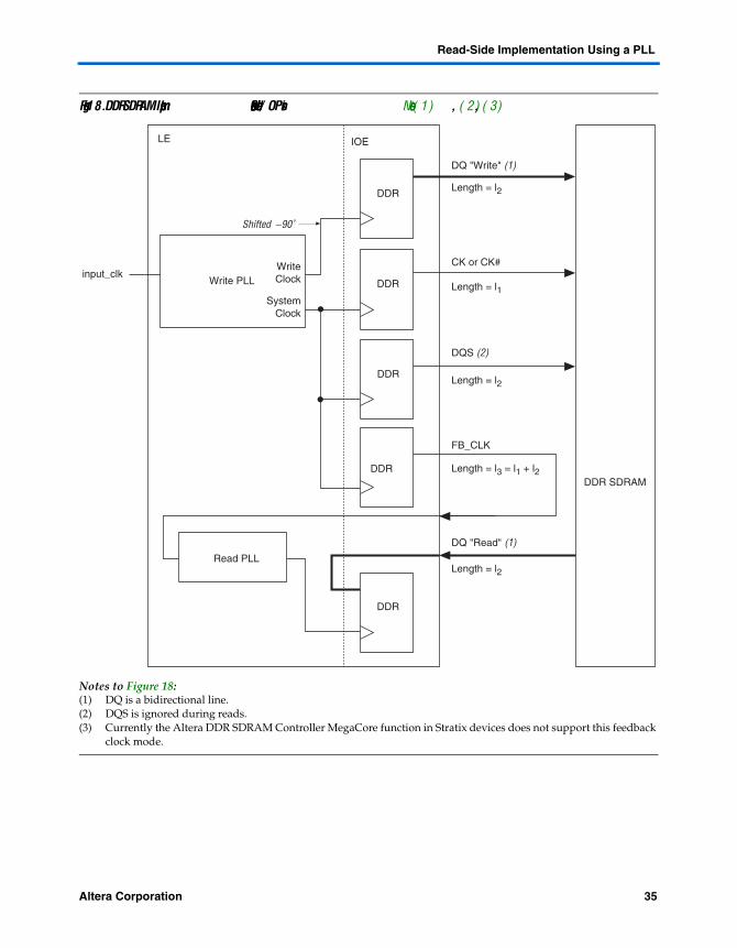
Read-Side Implementation Using a PLL
You can interface Stratix and Stratix GX devices with DDR SDRAM devices without using the DQS phase-shift circuitry. This section provides an example that uses two sets of PLLs (per I/O bank for best performance), a write PLL and a read PLL, and a feedback clock between the write PLL and the read PLL (Figure 18).
You can choose any of the user I/O pins for the DQ, DQS, and DM pins. The board trace lengths for the DQ, DQS, and DM pins should be tightly matched.
The write PLL generates the system clock, the –90° shifted clock, and the feedback clock, FB_CLK. The feedback clock is routed outside the FPGA and back into the FPGA. This board trace length should be equal to the clock trace length from the FPGA to the memory, plus the DQ trace length from the memory to the FPGA. If the clock trace length = l1 and the DQ trace length = l2, the FB_CLK must have a trace length of l3 = (l1 + l2) (see Figure 18).
The read PLL uses the feedback clock as the input clock and generates the clock needed to capture the DQ during reads. The DQS signal entering the FPGA is ignored in this scheme. The read PLL is in normal mode, so the PLL output at an LE register is in phase with the PLL input at the clock pin. Because the trace length of the feedback clock is the same as the CK/CK# and DQS trace, FB_CLK coming into the FPGA looks like the DQS signal with a little bit of skew. The read PLL can then be shifted to compensate for the skew and create the 90° PLL phase shift to capture the DQ signals during reads.
In the source synchronous mode, Enhanced PLLs compensate for clock delay to top/bottom I/O registers and Fast PLLs compensate for clock delay to side I/O registers. While implementing DDR SDRAM interfaces without the DQS phase-shift circuitry, use the corresponding PLL type for best matching between clock and data delays. The input pin to register delay chain within the IOE should be set to zero in Quartus II for all data pins.
34 Altera CorporationPreliminary
Read-Side Implementation Using a PLL
Figure 18. DDR SDRAM Implementation on Side I/O Pins Notes (1), (2), (3)
Notes to Figure 18:(1) DQ is a bidirectional line. (2) DQS is ignored during reads.(3) Currently the Altera DDR SDRAM Controller MegaCore function in Stratix devices does not support this feedback
clock mode.
Write PLL
DDR
Read PLL
DDR
DDR
DQS (2)
DQ "Read" (1)
IOELE
input_clkCK or CK#
DQ "Write" (1)
Length = l1
Length = l2
Length = l2
FB_CLK
Length = l3 = l1 + l2
Length = l2
DDR
DDR
SystemClock
WriteClock
DDR SDRAM
Shifted −90˚
Altera Corporation 35Preliminary
Interfacing DDR SDRAM with Stratix & Stratix GX Devices
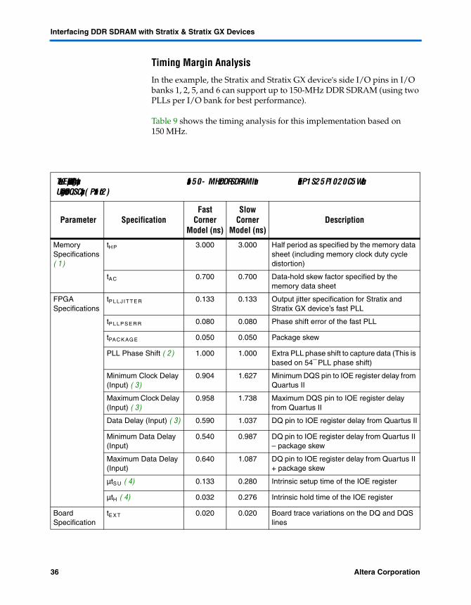
Timing Margin Analysis
In the example, the Stratix and Stratix GX device’s side I/O pins in I/O banks 1, 2, 5, and 6 can support up to 150-MHz DDR SDRAM (using two PLLs per I/O bank for best performance).
Table 9 shows the timing analysis for this implementation based on 150 MHz.
Table 9. Example Read Timing Analysis for 150-MHz DDR SDRAM Interface in EP1S25F1020C5 Without Using Dedicated DQS Circuitry (Part 1 of 2)
Parameter SpecificationFast
Corner Model (ns)
Slow Corner
Model (ns)Description
Memory Specifications (1)
tH P 3.000 3.000 Half period as specified by the memory data sheet (including memory clock duty cycle distortion)
tAC 0.700 0.700 Data-hold skew factor specified by the memory data sheet
FPGA Specifications
tP L L J I T T E R 0.133 0.133 Output jitter specification for Stratix and Stratix GX device’s fast PLL
tP L L P S E R R 0.080 0.080 Phase shift error of the fast PLL
tPAC K AG E 0.050 0.050 Package skew
PLL Phase Shift (2) 1.000 1.000 Extra PLL phase shift to capture data (This is based on 54° PLL phase shift)
Minimum Clock Delay (Input) (3)
0.904 1.627 Minimum DQS pin to IOE register delay from Quartus II
Maximum Clock Delay (Input) (3)
0.958 1.738 Maximum DQS pin to IOE register delay from Quartus II
Data Delay (Input) (3) 0.590 1.037 DQ pin to IOE register delay from Quartus II
Minimum Data Delay (Input)
0.540 0.987 DQ pin to IOE register delay from Quartus II – package skew
Maximum Data Delay (Input)
0.640 1.087 DQ pin to IOE register delay from Quartus II + package skew
µtS U (4) 0.133 0.280 Intrinsic setup time of the IOE register
µtH (4) 0.032 0.276 Intrinsic hold time of the IOE register
Board Specification
tE X T 0.020 0.020 Board trace variations on the DQ and DQS lines
36 Altera CorporationPreliminary
Read-Side Implementation Using a PLL
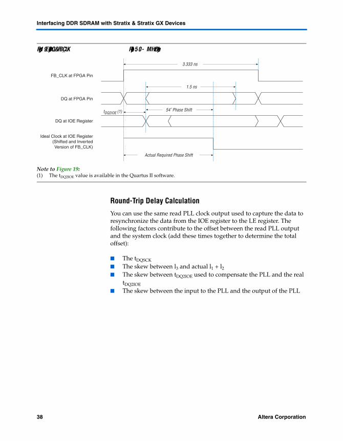
To calculate the read PLL phase shift, add the 54° shift with the delay from the DQ pin to the IOE (tDQ2IOE) register and account for the board trace length skew. The calculation will have some error due to the skew between DQ and CK from the memory itself. Figure 19 illustrates the DQ and FB_CLK signal relationship on a 150-MHz operation in an ideal situation.
Timing Calculation
tE A R LY _ C L O C K 1.691 2.414 Earliest possible clock edge after DQS phase-shift circuitry and uncertainties (minimum clock delay + PLL phase shift – tP L L J I T T E R – tP L L P S E R R)
tL AT E _ C L O C K 2.171 2.951 Latest possible clock edge after DQS phase-shift circuitry and uncertainties (maximum clock delay + PLL phase shift + tP L L J I T T E R + tP L L P S E R R)
tE A R LY _ DATA _ I NVA L I D 2.840 3.287 Time for earliest data to become invalid for sampling at FPGA flop (tH P – tAC + minimum data delay)
tL AT E _ DATA _ VA L I D 1.340 1.787 Time for latest data to become valid for sampling at FPGA flop (tAC + maximum data delay)
Results Read setup timing margin (2)
0.198 0.327 tE A RLY _ C L O C K – tL AT E _ DATA _ VA L I D – µtS U – tE X T
Read hold timing margin (2)
0.617 0.331 tE A RLY _ DATA _ I N VA L I D – tL AT E _ C L O C K – µtH – tE X T
Total margin 0.815 0.579 Setup margin + hold margin
Notes to Table 9:(1) The memory numbers used here come from Micron MT16VDDT3264A clocked at 150 MHz.(2) PLL phase shift is adjustable if you need to balance the setup and hold time margin.(3) These numbers are from the Quartus II software, version 5.0 SP1 using the Altera IP core DDR SDRAM Controller
version 3.2.0. Altera recommends using the latest version of the Quartus II software for your design.(4) These numbers are from the Quartus II software, version 5.0 SP1 using the Altera IP core DDR SDRAM Controller
version 3.2.0. Altera recommends using the latest version of the Quartus II software for your design.
Table 9. Example Read Timing Analysis for 150-MHz DDR SDRAM Interface in EP1S25F1020C5 Without Using Dedicated DQS Circuitry (Part 2 of 2)
Parameter SpecificationFast
Corner Model (ns)
Slow Corner
Model (ns)Description
Altera Corporation 37Preliminary
Interfacing DDR SDRAM with Stratix & Stratix GX Devices
Figure 19. Example of DQ & FB_CLK Relationship for 150-MHz Operation
Note to Figure 19:(1) The tDQ2IOE value is available in the Quartus II software.
Round-Trip Delay Calculation
You can use the same read PLL clock output used to capture the data to resynchronize the data from the IOE register to the LE register. The following factors contribute to the offset between the read PLL output and the system clock (add these times together to determine the total offset):
■ The tDQSCK
■ The skew between l3 and actual l1 + l2
■ The skew between tDQ2IOE used to compensate the PLL and the real tDQ2IOE
■ The skew between the input to the PLL and the output of the PLL
3.333 ns
1.5 ns
FB_CLK at FPGA Pin
DQ at FPGA Pin
DQ at IOE Register
Ideal Clock at IOE Register(Shifted and InvertedVersion of FB_CLK)
tDQ2IOE (1)
Actual Required Phase Shift
54˚ Phase Shift
38 Altera CorporationPreliminary
Write-Side Implementation
Write-Side Implementation
Whether you are using the DQS phase-shift circuitry or the PLL to capture data during a read operation from the DDR SDRAM device, there is only one implementation for the write operation. As shown in Figure 4 on page 10, the write side uses a PLL to generate the clocks listed in Table 10.
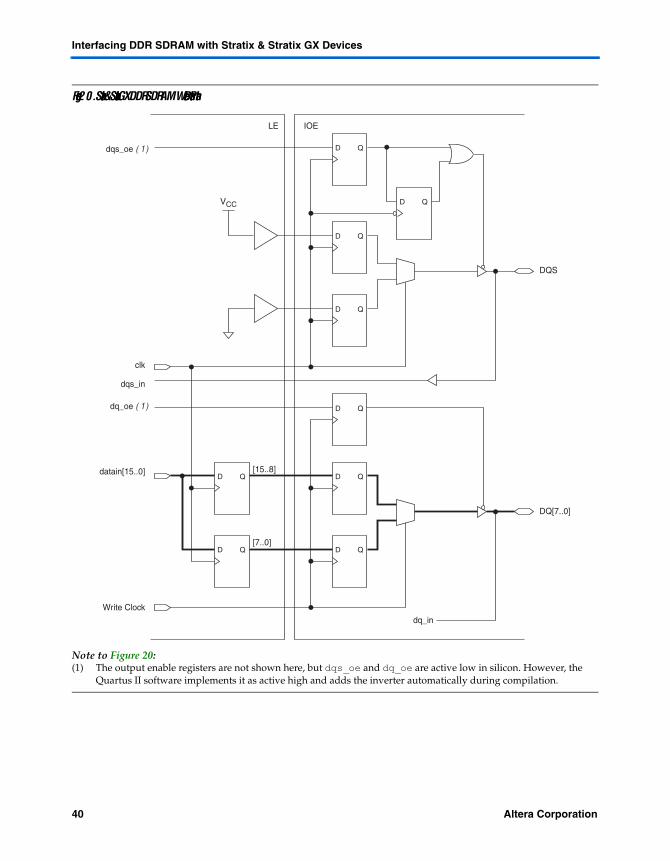
Figure 20 shows the data path for DDR SDRAM write operations.
Table 10. Clocks in a DDR SDRAM Interface
Clock Description
System clock Use this clock for the memory controller and to generate the DQS write and CK/CK# signals.
Write clock (–90° shifted from system clock)
Use this clock in the data path to generate the DQ write signals.
Feedback clock Use this optional clock only if you are not using the DQS phase-shift circuitry when reading from the DDR SDRAM device.
Resynchronization clock
Use this optional clock only if you are using the DQS phase-shift circuitry and need a different clock phase shift than available for resynchronization.
Altera Corporation 39Preliminary
Interfacing DDR SDRAM with Stratix & Stratix GX Devices
Figure 20. Stratix & Stratix GX DDR SDRAM Write Data Path
Note to Figure 20:(1) The output enable registers are not shown here, but dqs_oe and dq_oe are active low in silicon. However, the
Quartus II software implements it as active high and adds the inverter automatically during compilation.
DQS
clk
dqs_oe (1)
dqs_in
DQ[7..0]
datain[15..0]
Write Clock
dq_oe (1)
[15..8]
[7..0]
dq_in
VCC
D Q
D Q
D Q
D Q
D Q
D Q
D Q
D Q
D Q
LE IOE
40 Altera CorporationPreliminary
Write-Side Implementation
Write Timing Margin Analysis
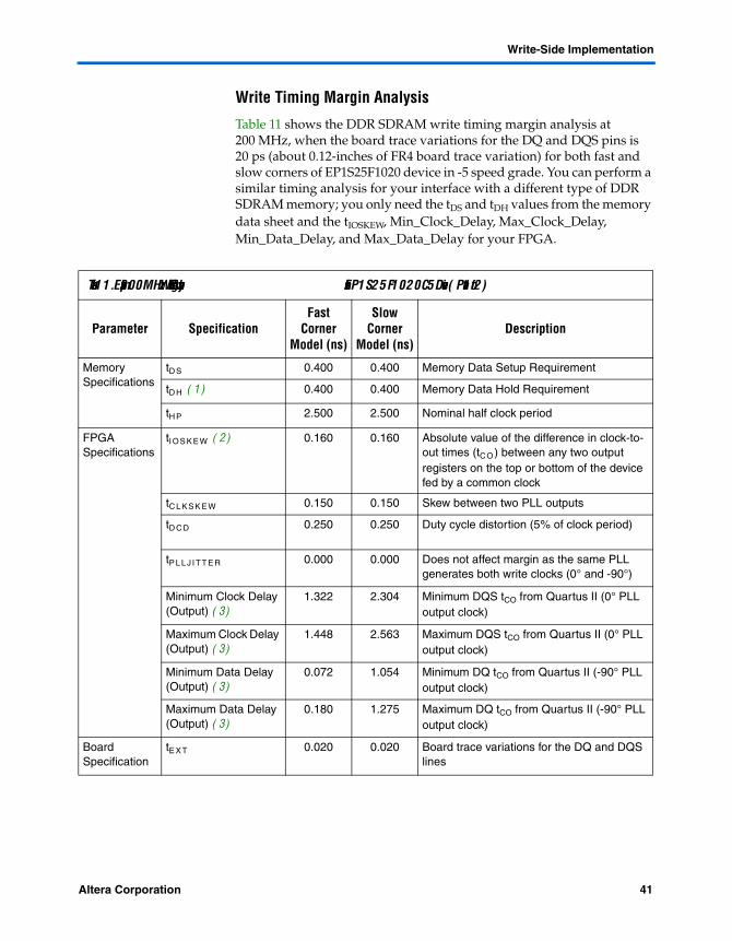
Table 11 shows the DDR SDRAM write timing margin analysis at 200 MHz, when the board trace variations for the DQ and DQS pins is 20 ps (about 0.12-inches of FR4 board trace variation) for both fast and slow corners of EP1S25F1020 device in -5 speed grade. You can perform a similar timing analysis for your interface with a different type of DDR SDRAM memory; you only need the tDS and tDH values from the memory data sheet and the tIOSKEW, Min_Clock_Delay, Max_Clock_Delay, Min_Data_Delay, and Max_Data_Delay for your FPGA.
Table 11. Example 200MHz Write Timing Analysis for an EP1S25F1020C5 Device (Part 1 of 2)
Parameter SpecificationFast
Corner Model (ns)
Slow Corner
Model (ns)Description
Memory Specifications
tD S 0.400 0.400 Memory Data Setup Requirement
tD H (1) 0.400 0.400 Memory Data Hold Requirement
tH P 2.500 2.500 Nominal half clock period
FPGA Specifications
tI O S K E W (2) 0.160 0.160 Absolute value of the difference in clock-to-out times (tCO) between any two output registers on the top or bottom of the device fed by a common clock
tC L K S K E W 0.150 0.150 Skew between two PLL outputs
tD CD 0.250 0.250 Duty cycle distortion (5% of clock period)
tP L L J I T T E R 0.000 0.000 Does not affect margin as the same PLL generates both write clocks (0° and -90°)
Minimum Clock Delay (Output) (3)
1.322 2.304 Minimum DQS tCO from Quartus II (0° PLL output clock)
Maximum Clock Delay (Output) (3)
1.448 2.563 Maximum DQS tCO from Quartus II (0° PLL output clock)
Minimum Data Delay (Output) (3)
0.072 1.054 Minimum DQ tCO from Quartus II (-90° PLL output clock)
Maximum Data Delay (Output) (3)
0.180 1.275 Maximum DQ tCO from Quartus II (-90° PLL output clock)
Board Specification
tE X T 0.020 0.020 Board trace variations for the DQ and DQS lines
Altera Corporation 41Preliminary
Interfacing DDR SDRAM with Stratix & Stratix GX Devices
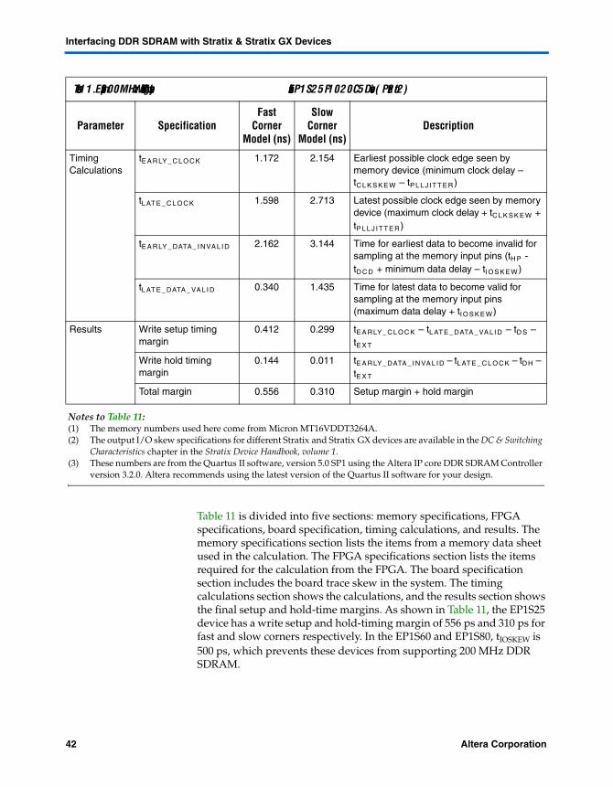
Table 11 is divided into five sections: memory specifications, FPGA specifications, board specification, timing calculations, and results. The memory specifications section lists the items from a memory data sheet used in the calculation. The FPGA specifications section lists the items required for the calculation from the FPGA. The board specification section includes the board trace skew in the system. The timing calculations section shows the calculations, and the results section shows the final setup and hold-time margins. As shown in Table 11, the EP1S25 device has a write setup and hold-timing margin of 556 ps and 310 ps for fast and slow corners respectively. In the EP1S60 and EP1S80, tIOSKEW is 500 ps, which prevents these devices from supporting 200 MHz DDR SDRAM.
Timing Calculations
tE A R LY _ C L O C K 1.172 2.154 Earliest possible clock edge seen by memory device (minimum clock delay – tC L K S K E W – tP L L J I T T E R)
tL AT E _ C L O C K 1.598 2.713 Latest possible clock edge seen by memory device (maximum clock delay + tC L K S K E W + tP L L J I T T E R)
tE A R LY _ DATA _ I NVA L I D 2.162 3.144 Time for earliest data to become invalid for sampling at the memory input pins (tH P - tD C D + minimum data delay – tI O S K E W)
tL AT E _ DATA _ VA L I D 0.340 1.435 Time for latest data to become valid for sampling at the memory input pins (maximum data delay + tI O S K E W)
Results Write setup timing margin
0.412 0.299 tE A RLY _ C L O C K – tL AT E _ DATA _ VA L I D – tD S – tE X T
Write hold timing margin
0.144 0.011 tE A RLY _ DATA _ I N VA L I D – tL AT E _ C L O C K – tDH – tE X T
Total margin 0.556 0.310 Setup margin + hold margin
Notes to Table 11:(1) The memory numbers used here come from Micron MT16VDDT3264A.(2) The output I/O skew specifications for different Stratix and Stratix GX devices are available in the DC & Switching
Characteristics chapter in the Stratix Device Handbook, volume 1.(3) These numbers are from the Quartus II software, version 5.0 SP1 using the Altera IP core DDR SDRAM Controller
version 3.2.0. Altera recommends using the latest version of the Quartus II software for your design.
Table 11. Example 200MHz Write Timing Analysis for an EP1S25F1020C5 Device (Part 2 of 2)
Parameter SpecificationFast
Corner Model (ns)
Slow Corner
Model (ns)Description
42 Altera CorporationPreliminary
Stratix & Stratix GX DDR Characterization Data
Stratix & Stratix GX DDR Characterization Data
The DDR SDRAM interface in Stratix and Stratix GX devices was characterized under worst-case conditions. The Altera DDR SDRAM Controller MegaCore function was used to access the DDR SDRAM module. For more information on the characterization setup, contact Altera Applications.
Board Design Guidelines
This section provides general guidelines for board design when using the DDR SDRAM Controller MegaCore function and Stratix and Stratix GX devices. It also provides information about decoupling capacitance. The following general guidelines apply when designing with Stratix and Stratix GX devices and DDR SDRAM.
■ Keep the memory component or DIMM and the Stratix and Stratix GX devices close together. The routing length between Stratix and Stratix GX devices and the DIMM should be within 4.5 inches.
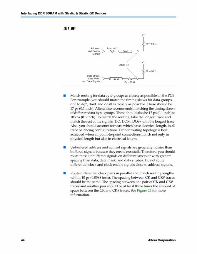
■ The locations of the series impedance-balancing resistors (RS) are important. For address and control signals, place these series-terminating resistors as close as possible to the Stratix and Stratix GX device. For data, data strobe, and data mask signals, place the series-terminating resistors as close as possible to the memory component or DIMM socket for the best signal integrity results. Pull-up resistors RT to VTT (1.25 V) are required for data, data strobe, data mask, address, and control signals and should be located after the end of the DIMM structure in a fly-by termination scheme. Routing length to the pull-ups is less critical, but most designs require 0.5 to 1 inch to route. Figure 21 shows this termination scheme.
1 These termination instructions are guidelines only. The best way to predict that the termination arrangement meets your requirements is to simulate your design, including the PCB and device packages. For more information, visit www.micron.com to obtain the Micron Technical Note TN-46-06: Termination for Point-to-Point Systems.
Altera Corporation 43Preliminary
Interfacing DDR SDRAM with Stratix & Stratix GX Devices
Figure 21. Termination Scheme
■ Match routing for data byte-groups as closely as possible on the PCB. For example, you should match the timing skews for data groups dq0 to dq7, dm0, and dqs0 as closely as possible. These should be 17 ps (0.1 inch). Altera also recommends matching the timing skews of different data byte-groups. These should also be 17 ps (0.1 inch) to 105 ps (0.5 inch). To match the routing, take the longest trace and match the rest of the signals (DQ, DQM, DQS) with the longest trace. Also, you should account for vias, which have electrical length, in all trace balancing configurations. Proper routing topology is best achieved when all point-to-point connections match not only in physical length but also in electrical length.
■ Unbuffered address and control signals are generally noisier than buffered signals because they create crosstalk. Therefore, you should route these unbuffered signals on different layers or with greater spacing than data, data mask, and data strobes. Do not route differential clock and clock enable signals close to address signals.
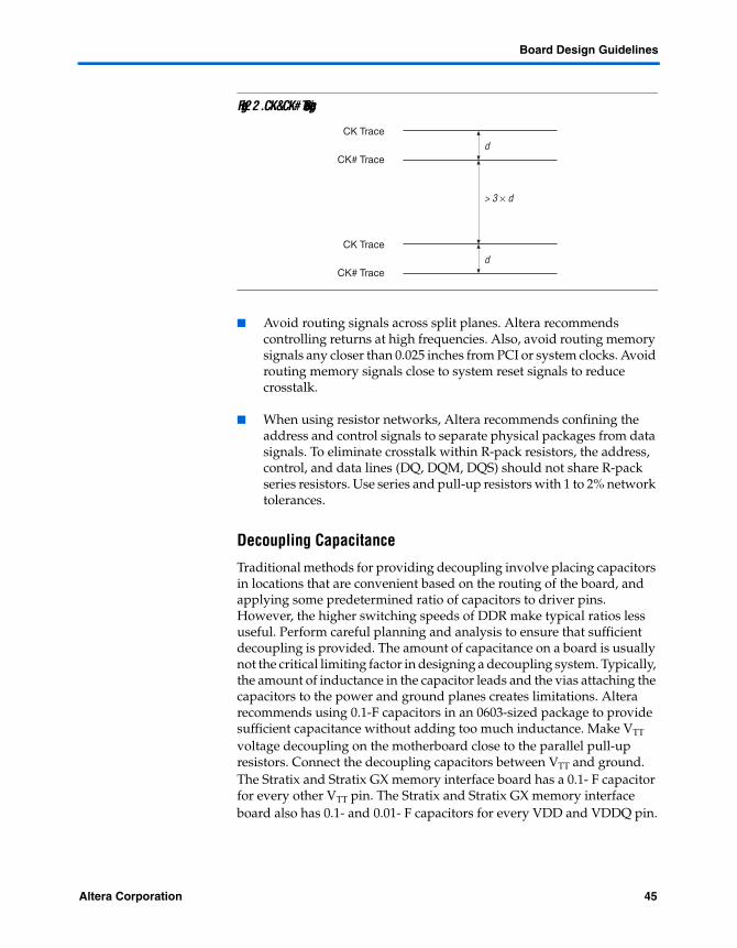
■ Route differential clock pairs in parallel and match routing lengths within 10 ps (0.0588 inch). The spacing between CK and CK# traces should be the same. The spacing between one pair of CK and CK# traces and another pair should be at least three times the amount of space between the CK and CK# traces. See Figure 22 for more information.
Address and Control
Signals
RS = 10 Ω
DIMM Pin
RT = 56 Ω
VTT
50 Ω
Data Strobe,Data Mask,
and Data Signals RS = 10 Ω
RT = 56 Ω
VTT
50 Ω
44 Altera CorporationPreliminary
Board Design Guidelines
Figure 22. CK & CK# Trace Spacing
■ Avoid routing signals across split planes. Altera recommends controlling returns at high frequencies. Also, avoid routing memory signals any closer than 0.025 inches from PCI or system clocks. Avoid routing memory signals close to system reset signals to reduce crosstalk.
■ When using resistor networks, Altera recommends confining the address and control signals to separate physical packages from data signals. To eliminate crosstalk within R-pack resistors, the address, control, and data lines (DQ, DQM, DQS) should not share R-pack series resistors. Use series and pull-up resistors with 1 to 2% network tolerances.
Decoupling Capacitance
Traditional methods for providing decoupling involve placing capacitors in locations that are convenient based on the routing of the board, and applying some predetermined ratio of capacitors to driver pins. However, the higher switching speeds of DDR make typical ratios less useful. Perform careful planning and analysis to ensure that sufficient decoupling is provided. The amount of capacitance on a board is usually not the critical limiting factor in designing a decoupling system. Typically, the amount of inductance in the capacitor leads and the vias attaching the capacitors to the power and ground planes creates limitations. Altera recommends using 0.1-F capacitors in an 0603-sized package to provide sufficient capacitance without adding too much inductance. Make VTT voltage decoupling on the motherboard close to the parallel pull-up resistors. Connect the decoupling capacitors between VTT and ground. The Stratix and Stratix GX memory interface board has a 0.1- F capacitor for every other VTT pin. The Stratix and Stratix GX memory interface board also has 0.1- and 0.01- F capacitors for every VDD and VDDQ pin.
CK Trace
CK# Trace
CK Trace
CK# Trace
d
d
> 3 × d
Altera Corporation 45Preliminary
Interfacing DDR SDRAM with Stratix & Stratix GX Devices
Conclusion Stratix and Stratix GX devices have dedicated circuitry to interface with up to 200-MHz DDR SDRAM with comfortable and consistent margins. The circuitry dynamically adjusts with PVT variations and can be fine-tuned for your system requirements. Stratix and Stratix GX devices use dedicated circuitry when reading from the memory and use the PLL when writing to the memory. This implementation simplifies board layout and controller design.
References JEDEC Standard Publication JESD79C, DDR SDRAM Specification, JEDEC Solid State Technology Association
MT16VDDT3264A, 184-Pin DDR SDRAM DIMMs Data Sheet, Micron Technology, Inc.
DDR SDRAM Controller MegaCore Function User Guide, Altera Corporation.
46 Altera CorporationPreliminary
101 Innovation DriveSan Jose, CA 95134(408) 544-7000www.altera.comApplications Hotline:(800) 800-EPLDLiterature Services:[email protected]
Copyright © 2005 Altera Corporation. All rights reserved. Altera, The Programmable Solutions Company,the stylized Altera logo, specific device designations, and all other words and logos that are identified astrademarks and/or service marks are, unless noted otherwise, the trademarks and service marks of AlteraCorporation in the U.S. and other countries. All other product or service names are the property of their re-spective holders. Altera products are protected under numerous U.S. and foreign patents and pendingapplications, maskwork rights, and copyrights. Altera warrants performance of its semiconductor productsto current specifications in accordance with Altera's standard warranty, but reserves the right to make chang-es to any products and services at any time without notice. Altera assumes no responsibility or liabilityarising out of the application or use of any information, product, or service describedherein except as expressly agreed to in writing by Altera Corporation. Altera customersare advised to obtain the latest version of device specifications before relying on any pub-lished information and before placing orders for products or services.