Embed Size (px)
Citation preview

DDR SDRAM
ASIC CourseSaeed BakhshiMay 2004Class presentation based on ISSCC2003 paper: A 1.8V, 700Mb/s/pin, 512Mb DDR-II SDRAM with On-Die Termination and Off-Chip Driver Calibration.

Outlines
Memory Evolution What is DDR? DDR Architecture High Speed Memory Design Considerations DDR-II Architecture
A 1.8V, 700Mb/s/pin, 512Mb DDR-II SDRAM with On-Die Termination and Off-Chip Driver Calibration A paper from:
ISSCC 2003; Session 17.8 Samsung Electronics

History of Memory
Memory Evolution 1979 DRAM 1997 SDRAM Next Generation Memories RAMBUS, DDR SDRAM
Only a few years ago, "regular" SDRAM was introduced as a proposed replacement for the older FPM and EDO asynchronous DRAM technologies. This was due to the limitations the older memory has when
working with systems using higher bus speeds (over 75 MHz). In the next couple of years, as system bus speeds increase
further, the bell will soon toll on SDRAM itself. One of the proposed new standards to replace SDRAM is
Double Data Rate SDRAM or DDR SDRAM.

What is DDR?
DDR (Double Data Rate) memory is the next generation SDRAM.
Like SDRAM, DDR is synchronous with the system clock. The big difference between DDR and SDRAM memory is that
DDR reads data on both the rising and falling edges of the clock signal.
SDRAM only carries information on the rising edge of a signal. Basically this allows the DDR module to transfer data twice as
fast as SDRAM. For example, instead of a data rate of 133MHz, DDR memory
transfers data at 266MHz. DDR SDRAM also consumes less power, which makes it ideal
for notebook computers. JESD79C is the JEDEC standard for DDR SDRAM
specifications.

DDR Terminology
Name Clock Freq. Data Rate
DDR200 100 MHZ 200 MHZ
DDR266 133 MHZ 266 MHZ
DDR333 167 MHZ 300 MHZ
DDR400 200 MHZ 400 MHZ

DDR Architecture
The DDR SDRAM uses a double data rate architecture to achieve high speed operation.
The double data rate architecture is essentially a 2n prefetch architecture, with an interface designed to transfer two data words per clock cycle at the I/O pins.
A single read or write access for the DDR SDRAM consists of : Single 2n-bit wide data, in one clock cycle is transferred at
the internal DRAM core. Two corresponding n-bit wide data, in two-half clock cycle,
are transferred at the I/O pins.

DDR Architecture

DDR Architecture
Data Input Sampling DIND : Input data after Din buffer PE : Pulse generated by the rising edge of DQS PO : Pulse generated by the falling edge of DQS PCK : Internal Pulse generated by the rising edge of CLK
DDR Architecture
Output Driver Voltage mode push-pull driver ; small rON

DDR Architecture
SSTL stands for Series Stub Terminated Logic and has been defined and standardized within JEDEC.
Series resistors are incorporated in the SSTL signaling technology for main memory applications.
These resistors can be very effective in dissipating any reflected wave energy traveling along the module traces and isolating the module stubs from the main memory bus.
Proper termination of the bus transmission lines, reducing signal reflections.
The result is improved signal quality, higher clock frequencies, and lower EMI emissions.
SSTL inputs are typically a differential pair common source amplifier with one input tied to the VTT reference. This type of circuit provides excellent gain and bandwidth.

High Speed Memory Design Considerations
The Signal integrity is an challenging issue in High speed design.
The following effects are more important in High Speed Design and can cause data corruption. Reflection Crosstalk and interference SSN (simultaneously switching noise)
Following solutions are employed to improve signal integrity. On die Termination (ODT) Off chip Driver Calibration (OCD) On die Decoupling

DDR II
In JEDEC, DDR-II targeting 667Mb/s/pin is being defined as an extension of DDR. Interface is defined at VDDQ=1.8V. SSTL bus structure has been modified for higher data
rate. ODT (On Die Termination) is employed for better signal
integrity. DDR2 SDRAM introduces features and functions
that go beyond the DDR SDRAM specification and enable DDR2 to operate at data rates of 400 MHz, 533 MHz, 667 MHz, and above.

DDR II
Normal DDR limitations at higher frequencies: Signal integrity Power Consumption
DDR2 Addresses these challenges by: Operating voltage is reduced from 2.5V to 1.8V Reduced core operating frequency Core frequency = 1/2 the I/O frequency
Special New Features: 4-bit pre-fetch On-die termination Off-chip driver calibration
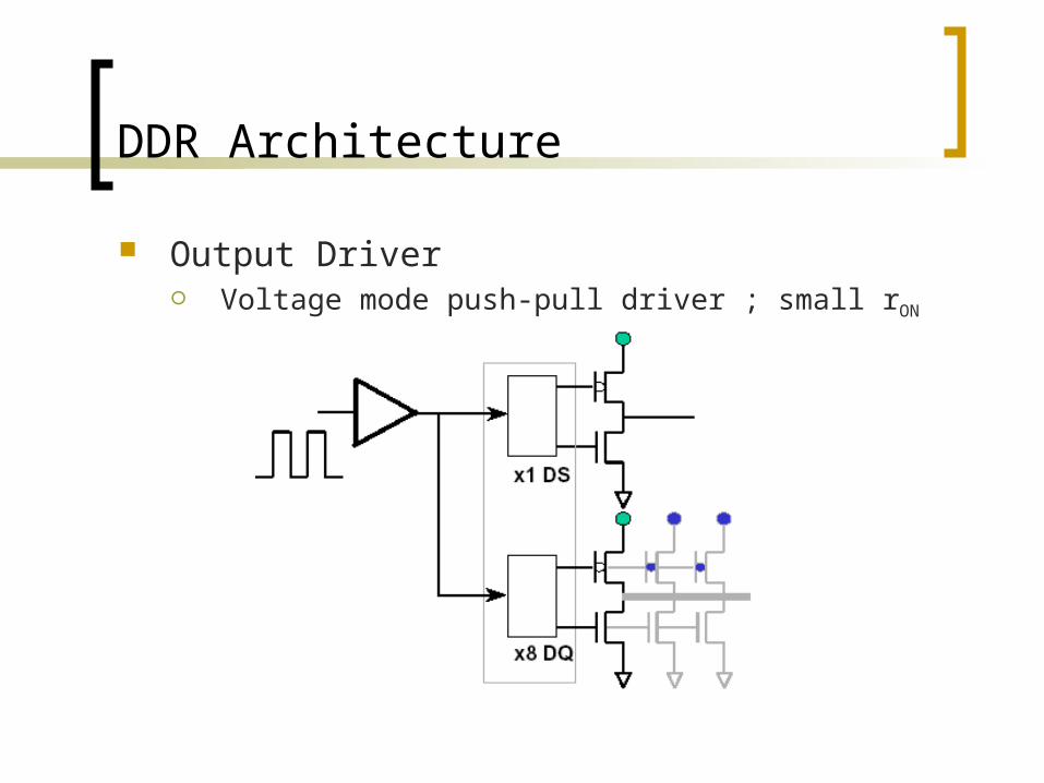
DDR Evolution

DDR and DDR-II

DDR-II Architecture

4-bit Pre-fetch
Single Data SDRAM In most DRAMs, the core and the I/O logic are running at the same
frequency. In SDRAM each output buffer can relase a single bit per clock cycle.
DDR (I) In DDR, every I/O buffer can output two bits per clock cycle. Each
read command will transfer two bits from the array into the DQ. Since the data are fetched from the array before they are released, the memory parlance describes this as "prefetch of 2". The simplest way to conceptualize this is to use two separate data lines
from the primary sense amps to the I/O buffers. The DQs are then outputting the data in a time multiplexed manner,
meaning one bit at a time on the same output line The easy way to do this is to collect the two bits in two separate pipeline
stages and then release them in the order of the queue on the rising and the falling edge of the clock.
Because two bits are released to the bus per pin and clock cycle, the protocol used is called double data rate or DDR.

4-bit Pre-fetch
DDR2 SDRAM achieves high-speed operation by 4-bit prefetch architecture. In 4-bit prefetch
architecture, DDR2 SDRAM can read/write 4 times the amount of data as an external bus from/to the memory cell array for every clock, and can be operated 4 times faster than the internal bus operation frequency.

ODT ( On-die termination )
On-die termination (ODT) has been added to the DDR2 data signals to improve signal integrity in the system.
The termination value of RTT is the Thevinen equivalent of the resistors that terminate the DQ inputs to VssQ and VDDQ.
An ODT pin is added to the DRAM so the system can turn the termination on and off as needed.

ODT (On Die Termination)

ODT (On Die Termination)

OCD( Off Chip Driver Calibration)
It is true that lower voltage swings enable higher frequencies but after a certain point, the ramping of the voltages will show a significant skew. The skew can be reduced by increased drive strength, however, with the
drawback of a voltage overshoot / undershoot at the rising and falling edges, respectively.
One additional problem with high frequency signaling is the phenomenon of trace delays. The solution in DDR was to add clock forwarding in form of a simple data
strobe. DDR II takes things further by introducing a bidirectional, differential I/O
buffer strobe consisting of DQS and /DQS as pull-up and pull-down signals.
Differential means that the two signals are measured against each other instead of using a simple strobe signal and a reference point.
In theory the pull-up and pull-down signals should be mirror-symmetric to each other but reality shows otherwise.

OCD( Off Chip Driver Calibration)
One way to solve the problem is to use Off-Chip Driver calibration (OCD calibration) where both parts of the differential strobes are calibrated against each other and against the DQ signal.
Through this sort of calibration, the ramping voltages are optimized for the buffer impedances to reduce over and undershooting at the rising and falling edges.
Without OCD calibration, the DRAM has a nominal output driver strength of 18 ohms +30% and a pull-up and pulldown mismatch of up to 4 ohms.
Using OCD calibration, a system can reduce the pull-up and pull-down mismatch and target the output driver at 18 ohms to optimize the signal integrity.

OCD( Off Chip Driver Calibration)

DDR, DDR2 Comparison Table
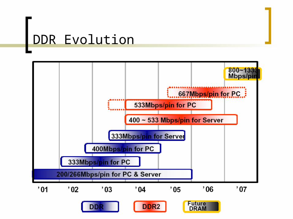
A 1.8V, 700Mb/s/pin, 512Mb DDR-II SDRAM with On-Die Termination and
Off-Chip Driver CalibrationC. Yoo, K. Kyung, G. Han, K. Lim, H. Lee, J. Chai, N. Heo,
G. Byun, D. Lee, H. Choi, H. Choi, C. Kim, S. Cho
Samsung Electronics, Hwa-Sung, Korea
Abstract: A 1.8V 700Mb/s/pin 512Mb DDR SDRAM is JEDEC standard compliant With the
hierarchical I/O line and local sensing.For signal integrity at 533Mb/s, off-chip driver
calibration and on-die termination are employed.
ISSCC 2003; Session17; SRAM and DRAM Memory
Contents
Introduction Data Path Architecture
Hierarchical I/O with Half-Vcc Precharge Signal Integrity (SI) Improvement
Off-Chip Driver (OCD) Calibration On-Die Termination (ODT)
Conclusion
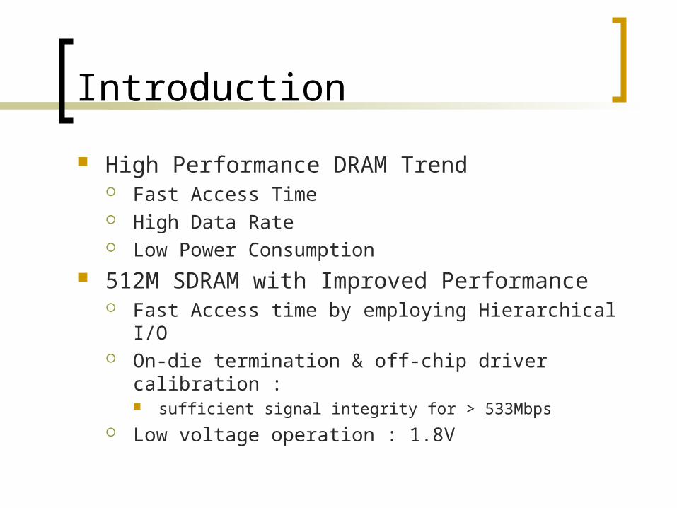
Introduction
High Performance DRAM Trend Fast Access Time High Data Rate Low Power Consumption
512M SDRAM with Improved Performance Fast Access time by employing Hierarchical I/O On-die termination & off-chip driver calibration :
sufficient signal integrity for > 533Mbps
Low voltage operation : 1.8V

CHIP Architecture
Data Path Architecture
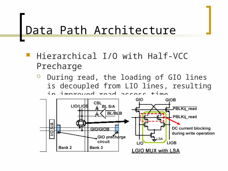
Hierarchical I/O with Half-VCC Precharge During read, the loading of GIO lines is
decoupled from LIO lines, resulting in improved read access time.

Data Path Architecture
For fast access time, the data lines from the array have hierarchical structure as local I/O (LIO) and global I/O (GIO) lines. The loading of GIO lines decoupled from LIO lines,
improves the read access time by 3.5ns.
The GIO/GIOB and LIO/LIOB lines are precharged to VccA/2. The Precharge time would be too long if the
Precharge level were VccA .
Real cycle time reduction by 4.23ns.

Data Path Architecture

Signal Integrity Improvement
Off-Chip Driver Calibration The strength of DRAM off-chip driver is
calibrated interactively. On-Die Termination
Termination resistors are placed inside DRAM and chipset instead of the motherboard.
Better signal integrity than motherboard terminated bus topology. timing improvement by 130 ps.

Off-Chip Driver Calibration
Variable strength for Drivers. During OCD calibration mode, chipset sets the
control codes.

On Die Termination
Same structure as OCD to have the same on/off delay as OCD delay.

Thank You