Embed Size (px)
Citation preview
1
Digital Logic
ObjectiveVerify proper operation of various logic gates.
Equipment List• Computer running Windows (NI ELVIS installed)• National Instruments DAQ board (inside computer).• Logic IC Chips (1 each of the following):
7408 Quad 2-input AND gate7432 Quad 2-input OR gate
• Wires for connecting the previous equipment together.
Discussion
Digital logic devices are the circuits that electronically performlogic operations on binary variables. The binary information isrepresented by high and low voltage levels, which the deviceprocesses electronically. The devices that perform the simplest ofthe logic operations (such as AND, OR, NAND, etc.) are calledgates. For example, an AND gate electronically computes theAND of the voltage encoded binary signals appearing at its inputsand presents the voltage encoded result at its output.
The digital logic circuits used in this laboratory are contained inintegrated circuit (IC) packages. Each IC is labeled (usually withan SN74xx or SN54xx number) to identify the logic it performs.The transistor-transistor logic(TTL) IC’s used in this laboratoryrequire a 5.0 volt power supply for operation. TTL inputs require avoltage greater than 2 volts to represent a binary 1 and a voltageless than 0.8 volts to represent a binary 0.
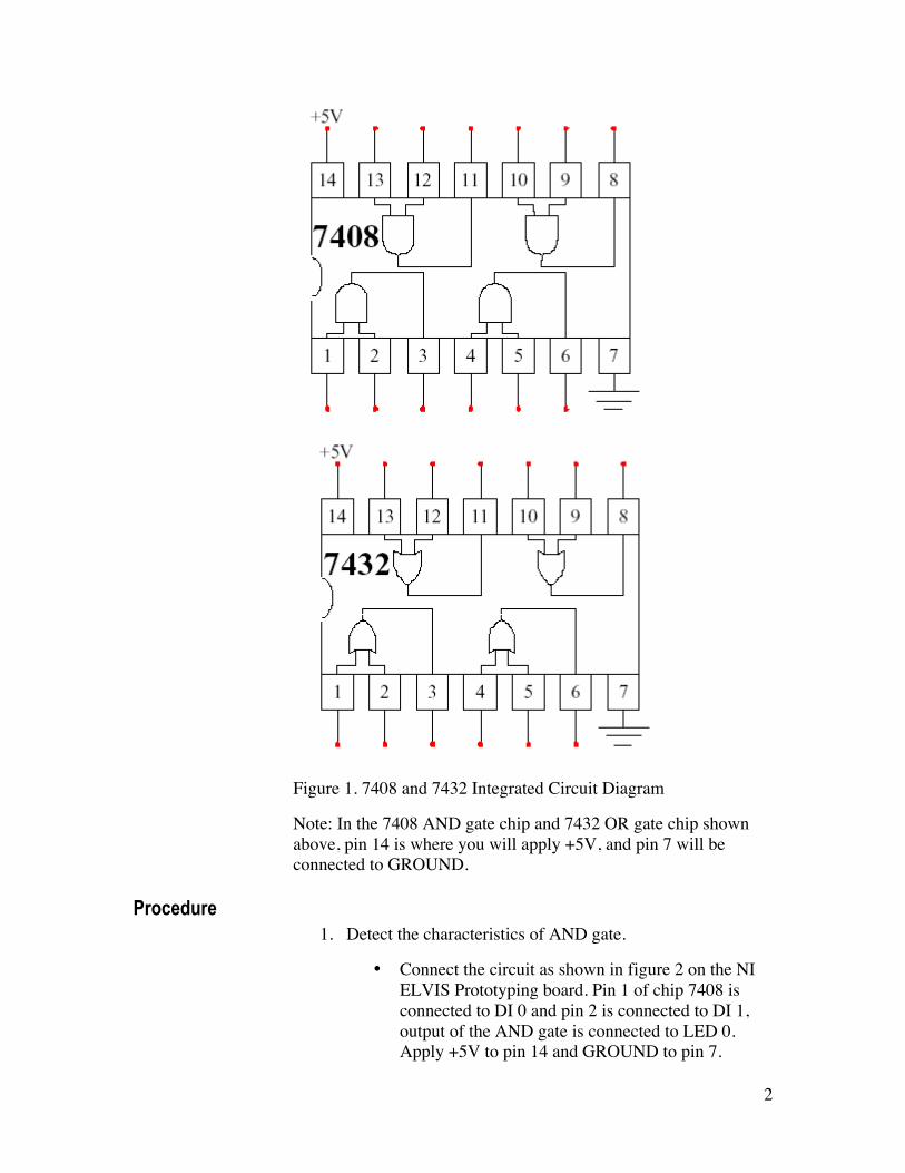
Integrated CircuitsThe small integrated circuits used in this lab implement basic logicgates. Some of the pins are inputs to the gates, others are outputs,and two of them are the connectors for power (+5V) andGROUND (0V). See figure 1.
2
Figure 1. 7408 and 7432 Integrated Circuit Diagram
Note: In the 7408 AND gate chip and 7432 OR gate chip shownabove, pin 14 is where you will apply +5V, and pin 7 will beconnected to GROUND.
Procedure1. Detect the characteristics of AND gate.
• Connect the circuit as shown in figure 2 on the NIELVIS Prototyping board. Pin 1 of chip 7408 isconnected to DI 0 and pin 2 is connected to DI 1,output of the AND gate is connected to LED 0.Apply +5V to pin 14 and GROUND to pin 7.

3
Figure 2. Component Layout for AND gate
• Turn on the NI ELVIS Benchtop Workstation,select Start»Programs»National Instruments»NIELVIS 1.0»NI ELVIS, or select NI ELVIS on thedesktop.
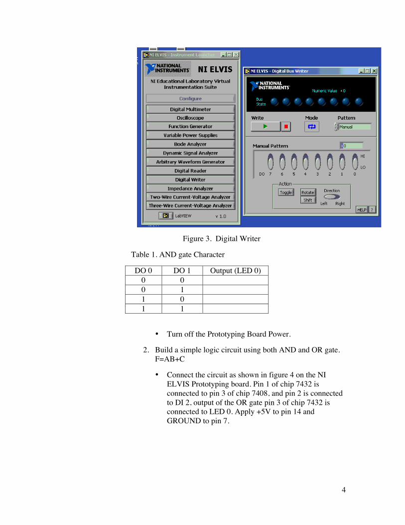
• Click the Digital Writer on the NI ELVISsoftware, as figure 3 shown. Set DO 0 and DO1 asshown in table 1, observe the output of the LED 0.If LED 0 light is on, that means logic 1, and if it isoff that means logic 0. Whenever set a digital valueof DO 0 and DO 1, click Write to write the logicvalue to DI 0 and DI 1 of the prototyping board.
• Observe the Output (LED 0) on the PrototypingBoard; write the output to Table 1.
4
Figure 3. Digital Writer
Table 1. AND gate Character
DO 0 DO 1 Output (LED 0)0 00 11 01 1
• Turn off the Prototyping Board Power.
2. Build a simple logic circuit using both AND and OR gate.F=AB+C
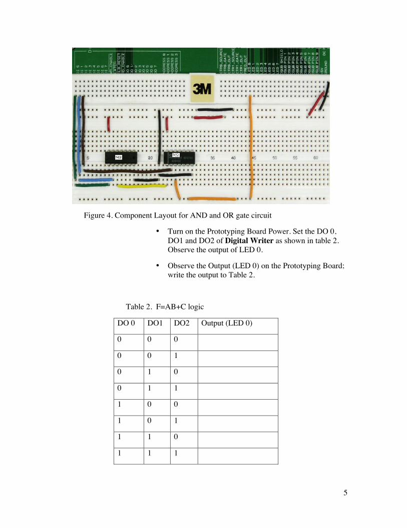
• Connect the circuit as shown in figure 4 on the NIELVIS Prototyping board. Pin 1 of chip 7432 isconnected to pin 3 of chip 7408, and pin 2 is connectedto DI 2, output of the OR gate pin 3 of chip 7432 isconnected to LED 0. Apply +5V to pin 14 andGROUND to pin 7.
5
Figure 4. Component Layout for AND and OR gate circuit
• Turn on the Prototyping Board Power. Set the DO 0,DO1 and DO2 of Digital Writer as shown in table 2.Observe the output of LED 0.
• Observe the Output (LED 0) on the Prototyping Board;write the output to Table 2.
Table 2. F=AB+C logic
DO 0 DO1 DO2 Output (LED 0)
0 0 0
0 0 1
0 1 0
0 1 1
1 0 0
1 0 1
1 1 0
1 1 1

6