Embed Size (px)
DESCRIPTION
it includes ideas about digital electonics family members such as opam mosfet bla bla...well read it n find urself then
Citation preview

4.1 INTRODUCTION
The switching characteristics of semiconductor devices have been discussed in Chapter 3.Basically, there are two types of semiconductor devices: bipolar and unipolar. Based on thesedevices, digital integrated circuits have been made which are commercially available. Variousdigital functions are being fabricated in a variety of forms using bipolar and unipolar technolo-gies. A group of compatible ICs with the same logic levels and supply voltages for performingvarious logic functions have been fabricated using a specific circuit configuration which isreferred to as a logic family.
4.1.1 Bipolar Logic Families
The main elements of a bipolar IC are resistors, diodes (which are also capacitors) and transis-tors. Basically, there are two types of operations in bipolar ICs:
1. Saturated, and2. Non-saturated.
In saturated logic, the transistors in the IC are driven to saturation, whereas in the case ofnon-saturated logic, the transistors are not driven into saturation.
The saturated bipolar logic families are:1. Resistor–transistor logic (RTL),2. Direct–coupled transistor logic (DCTL),3. Integrated–injection logic (I2L),4. Diode–transistor logic (DTL),5. High–threshold logic (HTL), and6. Transistor-transistor logic (TTL).
4
DIGITAL LOGIC FAMILIES
90 Modern Digital Electronics
The non-saturated bipolar logic families are:1. Schottky TTL, and2. Emitter-coupled logic (ECL).
4.1.2 Unipolar Logic Families
MOS devices are unipolar devices and only MOSFETs are employed in MOS logic circuits.The MOS logic families are:
1. PMOS,2. NMOS, and3. CMOS
While in PMOS only p-channel MOSFETs are used and in NMOS only n-channel MOSFETsare used, in complementary MOS (CMOS), both p- and n-channel MOSFETs are employedand are fabricated on the same silicon chip.
All the above logic families are discussed in this chapter.
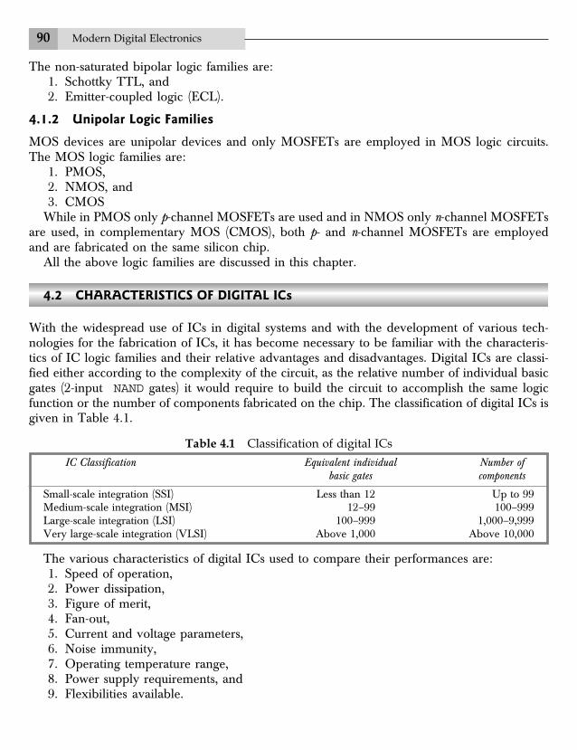
4.2 CHARACTERISTICS OF DIGITAL ICs
With the widespread use of ICs in digital systems and with the development of various tech-nologies for the fabrication of ICs, it has become necessary to be familiar with the characteris-tics of IC logic families and their relative advantages and disadvantages. Digital ICs are classi-fied either according to the complexity of the circuit, as the relative number of individual basicgates (2-input NAND gates) it would require to build the circuit to accomplish the same logicfunction or the number of components fabricated on the chip. The classification of digital ICs isgiven in Table 4.1.
Table 4.1 Classification of digital ICsIC Classification Equivalent individual Number of
basic gates components
Small-scale integration (SSI) Less than 12 Up to 99Medium-scale integration (MSI) 12–99 100–999Large-scale integration (LSI) 100–999 1,000–9,999Very large-scale integration (VLSI) Above 1,000 Above 10,000
The various characteristics of digital ICs used to compare their performances are:1. Speed of operation,2. Power dissipation,3. Figure of merit,4. Fan-out,5. Current and voltage parameters,6. Noise immunity,7. Operating temperature range,8. Power supply requirements, and9. Flexibilities available.

Digital Logic Families 91
4.2.1 Speed of Operation
The speed of a digital circuit is specified in termsof the propagation delay time. The input andoutput waveforms of a logic gate are shown inFig. 4.1. The delay times are measured betweenthe 50 per cent voltage levels of input and out-put waveforms. There are two delay times: tpHL,when the output goes from the HIGH state tothe LOW state and tpLH, corresponding to theoutput making a transition from the LOW stateto the HIGH state. The propagation delay timeof the logic gate is taken as the average of thesetwo delay times.
4.2.2 Power Dissipation
This is the amount of power dissipated in an IC. It is determined by the current, ICC , that itdraws from the VCC supply, and is given by VCC ¥ ICC . ICC is the average value of ICC (0) andICC (1). This power is specified in milliwatts.
4.2.3 Figure of Merit
The figure of merit of a digital IC is defined as the product of speed and power. The speed isspecified in terms of propagation delay time expressed in nanoseconds.
Figure of merit = propagation delay time (ns) ¥ power (mW)
It is specified in pico joules (ns ¥ mW = pJ)A low value of speed-power product is desirable. In a digital circuit, if it is desired to have
high speed, i.e. low propagation delay, then there is a corresponding increase in the powerdissipation and vice-versa.
4.2.4 Fan-Out
This is the number of similar gates which can be driven by a gate. High fan-out is advantageousbecause it reduces the need for additional drivers to drive more gates.
4.2.5 Current and Voltage Parameters
The following currents and voltages are specified which are very useful in the design of digitalsystems.
High-level input voltage, VIH : This is the minimum input voltage which is recognized by thegate as logic 1.
Low-level input voltage, VIL: This is the maximum input voltage which is recognized by thegate as logic 0.
High-level output voltage, VOH : This is the minimum voltage available at the output corre-sponding to logic 1.
Low-level output voltage, VOL: This is the maximum voltage available at the output correspond-ing to logic 0.
Input
Output
50%
tpHL tpLH
50%
Fig. 4.1Input and output voltage waveforms todefine propagation delay times.

92 Modern Digital Electronics
High-level input current, IIH : This is the minimum current which must be supplied by a drivingsource corresponding to 1 level voltage.
Low-level input current, IIL: This is the minimum current which must be supplied by a drivingsource corresponding to 0 level voltage.
High-level output current, IOH : This is the maximum current which the gate can sink in 1 level.Low-level output current, IOL: This is the maximum cur-
rent which the gate can sink in 0 level.High-level supply current, ICC (1): This is the supply cur-
rent when the output of the gate is at logic 1.Low-level supply current, ICC (0): This is the supply cur-
rent when the output of the gate is at logic (0).The current directions are illustrated in Fig. 4.2.
4.2.6 Noise Immunity
The input and output voltage levels defined aboveare shown in Fig. 4.3. Stray electric and magneticfields may induce unwanted voltages, known asnoise, on the connecting wires between logic cir-cuits. This may cause the voltage at the input to alogic circuit to drop below VIH or rise above VILand may produce undesired operation. The circuit’sability to tolerate noise signals is referred to as thenoise immunity, a quantitative measure of which iscalled noise margin. Noise margins are illustrated inFig. 4.3.
The noise margins defined above are referredto as dc noise margins. Strictly speaking, the noise isgenerally thought of as an a.c. signal with ampli-tude and pulse width. For high speed ICs, a pulsewidth of a few microseconds is extremely long in comparison to the propagation delay time ofthe circuit and therefore, may be treated as d.c. as far as the response of the logic circuit isconcerned. As the noise pulse width decreases and approaches the propagation delay time ofthe circuit, the pulse duration is too short for the circuit to respond. Under this condition, alarge pulse amplitude would be required to produce a change in the circuit output. This meansthat a logic circuit can effectively tolerate a large noise amplitude if the noise is of a very shortduration. This is referred to as ac noise margin and is substantially greater than the dc noisemargin. It is generally supplied by the manufacturers in the form of a curve between noisemargin and noise pulse width.
4.2.7 Operating Temperature
The temperature range in which an IC functions properly must be known. The acceptedtemperature ranges are: 0 to + 70 °C for consumer and industrial applications and –55 °C to+ 125 °C for military purposes.
IIL
IIH
IOL
IOH
Fig. 4.2A gate with current directionsmarked.
Fig. 4.3Voltage levels and noise margins of ICs.
Voltages
0 State noise margin D 0 = VIL – VOL
1 State noise margin D 1= VOH – VIH
VOH
VIH
VIL
VOL
0
Digital Logic Families 93
4.2.8 Power Supply Requirements
The supply voltage(s) and the amount of power required by an IC are important characteristicsrequired to choose the proper power supply.
4.2.9 Flexibilities Available
Various flexibilities are available in different IC logic families and these must be consideredwhile selecting a logic family for a particular job. Some of the flexibilities available are:
1. The breadth of the series: Type of different logic functions available in the series.2. Popularity of the series: The cost of manufacturing depends upon the number of ICs
manufactured. When a large number of ICs of one type are manufactured, the cost perfunction will be very small and it will be easily available because of multiple sources.
3. Wired-logic capability: The outputs can be connected together to perform additional logicwithout any extra hardware.
4. Availability of complement outputs: This eliminates the need for additional inverters.5. Type of output: Passive pull-up, active pull-up, open-collector/drain, and tristate. These
will be explained in subsequent sections.
4.3 RESISTOR–TRANSISTOR LOGIC (RTL)
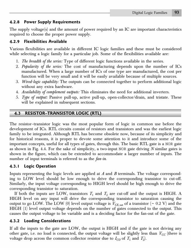
The resistor–transistor logic was the most popular form of logic in common use before thedevelopment of ICs. RTL circuits consist of resistors and transistors and was the earliest logicfamily to be integrated. Although RTL has become obsolete now, because of its simplicity andfor historical reasons, it is proper to devote some attention to it and introduce some of theimportant concepts, useful for all types of gates, through this. The basic RTL gate is a NOR gateas shown in Fig. 4.4. For the sake of simplicity, a two-input NOR gate driving N similar gates isshown in the figure, which can be extended to accommodate a larger number of inputs. Thenumber of input terminals is referred to as the fan-in.
4.3.1 Logic Operation
Inputs representing the logic levels are applied at A and B terminals. The voltage correspond-ing to LOW level should be low enough to drive the corresponding transistor to cut-off.Similarly, the input voltage corresponding to HIGH level should be high enough to drive thecorresponding transistor to saturation.
If both the inputs are LOW, transistors T1 and T2 are cut-off and the output is HIGH. AHIGH level on any input will drive the corresponding transistor to saturation causing theoutput to go LOW. The LOW (0) level output voltage is VCE , sat of a transistor (~ 0.2 V) and theHIGH (1) level output voltage depends on the number of gates connected to the output. Thiscauses the output voltage to be variable and is a deciding factor for the fan-out of the gate.
4.3.2 Loading Considerations
If all the inputs to the gate are LOW, the output is HIGH and if the gate is not driving anyother gate, i.e. no load is connected, the output voltage will be slightly less than VCC (there isvoltage drop across the common collector resistor due to ICO of T1 and T2).
94 Modern Digital Electronics
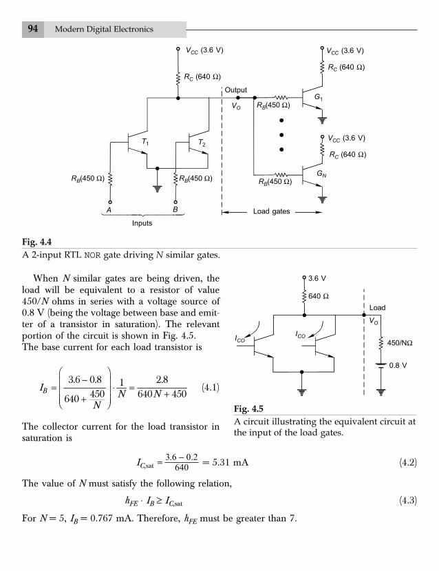
When N similar gates are being driven, theload will be equivalent to a resistor of value450/N ohms in series with a voltage source of0.8 V (being the voltage between base and emit-ter of a transistor in saturation). The relevantportion of the circuit is shown in Fig. 4.5.The base current for each load transistor is
IB3.6 0.8 2.81
450 640 450640 N NN
Ê ˆ-Á ˜= ◊ =Á ˜ ++Á ˜Ë ¯
(4.1)
The collector current for the load transistor insaturation is
IC,sat = −3 6 0 2640. . = 5.31 mA (4.2)
The value of N must satisfy the following relation,
hFE ◊ IB ≥ IC,sat (4.3)
For N = 5, IB = 0.767 mA. Therefore, hFE must be greater than 7.
VCC (3.6 V)
RC (640 W)
Output
VCC (3.6 V)
RC (640 W)
VO
G1
VCC (3.6 V)
RC (640 W)
RB(450 W)
RB(450 W)
T1 T2
RB(450 W)
Load gatesA B
Inputs
GNRB(450 W)
Fig. 4.4A 2-input RTL NOR gate driving N similar gates.
3.6 V
ICO
VO
Load
450/NW
0.8 V
ICO
Fig. 4.5A circuit illustrating the equivalent circuit atthe input of the load gates.
640 W
Digital Logic Families 95
4.3.3 Noise Margins
When the output is in 0 state VO = 0.2 V. If this voltage becomes about 0.5 V (cut-in voltage oftransistor), the load transistor comes to conduction which causes malfunction of the circuit.Hence, the logic 0 noise margin D 0 ª 0.3 V.
The logic 1 noise margin depends upon the number of gates being driven. For N = 5,
VO 90 640(3.6) (0.8) 1.14 V90 640 90 640
= ¥ + ¥ =+ +
(4.4)
For hFE = 10, the total base current required for load transistors to be driven into saturation will
be 5 ¥ 5.3110
Ê ˆÁ ˜Ë ¯
mA and the corresponding VO must be 1.04 V. Therefore, the noise margin for
1 level is D 1 = 1.14 – 1.04 = 0.1 V.
4.3.4 Propagation Delay Time
The propagation delay time is also affected by the number of gates it drives. When the outputof the gate is in LOW state all the load transistors are cut-off and the base–emitter junction ofeach of these transistors appears to be a capacitor, C . When the output has to change fromLOW to HIGH level due to changes at the input, it will do so with a time constant given by
( )450640N
+ NC = (640N + 450) C (4.5)
The resistance in the collector circuit pulls up the output voltage from LOW to HIGH leveland hence is known as the pull-up resistor. It is passive pull-up in this case in contrast to an activepull-up which can be used to decrease the propagation delay time. Active pull-up will bediscussed later.
4.3.5 Current Source Logic
The gate supplies current to the load transistors when in 1 level, whereas the leakage-current(reverse-saturation base current) of load transistors flow through T1 or T2 in 0 level. Since thesource current is much greater than the sink current, it is known as current source logic.
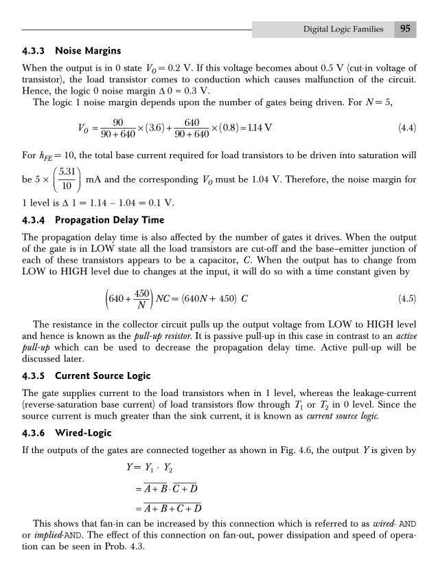
4.3.6 Wired-Logic
If the outputs of the gates are connected together as shown in Fig. 4.6, the output Y is given by
Y = Y1 ◊ Y2
A B C D= + ◊ +
A B C D= + + +This shows that fan-in can be increased by this connection which is referred to as wired- AND
or implied-AND. The effect of this connection on fan-out, power dissipation and speed of opera-tion can be seen in Prob. 4.3.
96 Modern Digital Electronics
The characteristics of RTL can be summarized as: Poor noise margin, poor fan-out capabili-ties, low speed, and high power dissipation.
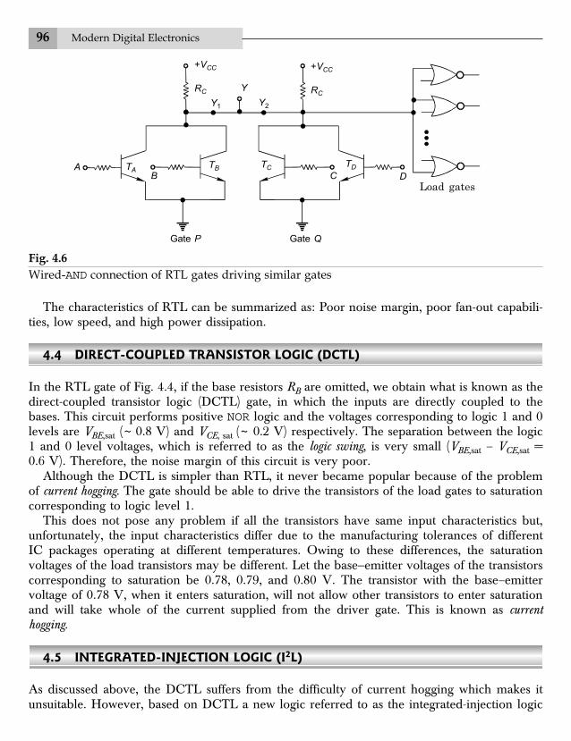
4.4 DIRECT-COUPLED TRANSISTOR LOGIC (DCTL)
In the RTL gate of Fig. 4.4, if the base resistors RB are omitted, we obtain what is known as thedirect-coupled transistor logic (DCTL) gate, in which the inputs are directly coupled to thebases. This circuit performs positive NOR logic and the voltages corresponding to logic 1 and 0levels are VBE,sat (~ 0.8 V) and VCE, sat (~ 0.2 V) respectively. The separation between the logic1 and 0 level voltages, which is referred to as the logic swing, is very small (VBE,sat – VCE,sat =0.6 V). Therefore, the noise margin of this circuit is very poor.
Although the DCTL is simpler than RTL, it never became popular because of the problemof current hogging. The gate should be able to drive the transistors of the load gates to saturationcorresponding to logic level 1.
This does not pose any problem if all the transistors have same input characteristics but,unfortunately, the input characteristics differ due to the manufacturing tolerances of differentIC packages operating at different temperatures. Owing to these differences, the saturationvoltages of the load transistors may be different. Let the base-emitter voltages of the transistorscorresponding to saturation be 0.78, 0.79, and 0.80 V. The transistor with the base–emittervoltage of 0.78 V, when it enters saturation, will not allow other transistors to enter saturationand will take whole of the current supplied from the driver gate. This is known as currenthogging.
4.5 INTEGRATED-INJECTION LOGIC (I2L)
As discussed above, the DCTL suffers from the difficulty of current hogging which makes itunsuitable. However, based on DCTL a new logic referred to as the integrated-injection logic
+VCC
RC Y
+VCC
RC
TC
C
TD
Gate P Gate Q
B DLoad gates
Fig. 4.6Wired-AND connection of RTL gates driving similar gates
Y2Y1
A TATB
Digital Logic Families 97
(I2L), has been developed. I2L has the simplicity of DCTL, uses very small silicon chip area,consumes very little power, and requires only four masks and two diffusions (compared to fivemasks and three diffusions for BJT) and hence, is easier and cheaper to fabricate. Due to theseadvantages it is eminently suited for medium- and large-scale integration. It is not used forsmall-scale integration and is the only saturated bipolar logic employed for large-scale integra-tion. Texas Instruments SBP 9900 is a 16-bit microprocessor using I2L technology.
The genesis of I2L technology is the concept of merging the components, viz. one semicon-ductor region is part of two or more devices. Because of this type of merging it is also referredto as the merged-transistor logic (MTL). There is considerable saving in the silicon chip area inthis process.
4.5.1 I2L Inverter
The basic operation of I2L is explained with the help of the inverter circuit shown in Fig. 4.7. Ifthe input Vi is at LOW logic level (Vi ª 0), T1 is OFF so that IB1 = 0. The input source acts as asink for the current I1. Therefore, I2 flows through the base of T2 driving it to saturation. WhenT1 is OFF and T2 is ON, VBE2 = VCE1 ª 0.8 V.
VO
Vi T1
+
–
VCE1
IB2
T2+
–VBE2
Fig. 4.7An I2L inverter directly coupled to the following stage.
On the other hand, if the input is at HIGH logic level (V1 ª 0.8 V), the base current IB1 willhave two components, one of them being I1 and the other is due to the source Vi , andconsequently T1 saturates. Therefore, VCE1 = VCE,sat ª 0.2 V, which drives T2 to cut-off and T1acts as a sink for I2. This shows that the logic level at VO is complement to that of Vi , viz. T1 actsas an inverter. The logic swing is about 0.6 V.
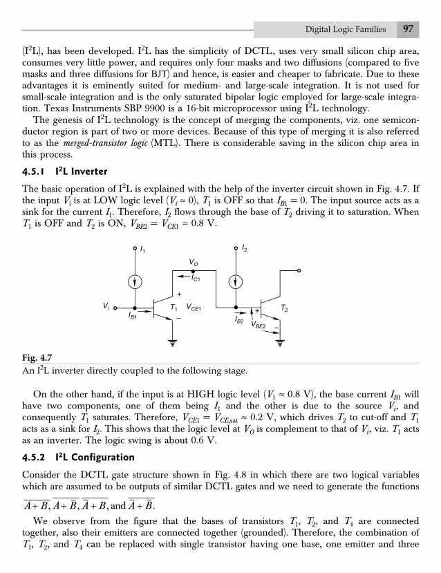
4.5.2 I2L Configuration
Consider the DCTL gate structure shown in Fig. 4.8 in which there are two logical variableswhich are assumed to be outputs of similar DCTL gates and we need to generate the functions
, , , and .A B A B A B A B+ + + +We observe from the figure that the bases of transistors T1, T2, and T4 are connected
together, also their emitters are connected together (grounded). Therefore, the combination ofT1, T2, and T4 can be replaced with single transistor having one base, one emitter and three
I1 I2
IC1
IB1
98 Modern Digital Electronics
VCC
RC
T2 T3
T4 T5
T6 T7
T9
T1 T10
VCC
RC
VCC
RC
VCC
RC
VCC
RC
VCC
RC
VCC
RC
A B
Fig. 4.8A DCTL gate structure for generating functions of two logical variables.
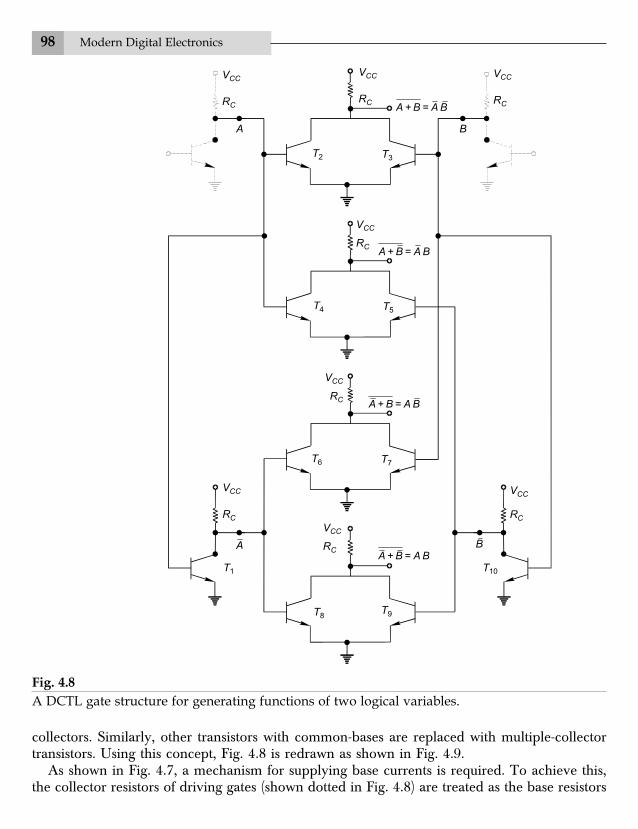
collectors. Similarly, other transistors with common-bases are replaced with multiple-collectortransistors. Using this concept, Fig. 4.8 is redrawn as shown in Fig. 4.9.
As shown in Fig. 4.7, a mechanism for supplying base currents is required. To achieve this,the collector resistors of driving gates (shown dotted in Fig. 4.8) are treated as the base resistors
VCC
RC
T8
� � � �� �
� � � �� �
� � � �� �
�� � � �� �
�
Digital Logic Families 99
VBB VBB VBB VBB
RB RB RB RB
C1 C6
C5
T ¢1 T ¢2 T ¢3 T ¢4BA
C10
Fig. 4.9Figure 4.8 redrawn with multiple-collector transistors.
of multiple-collector transistors (T ¢1 and T ¢3). Similarly, the collector resistors of T1 and T10 aretreated as the base resistors of T ¢2 and T ¢4, respectively. Correspondingly, the supply voltagesare indicated as VBB. The portion of the circuit shown outside the dotted box is either a part ofother gates driven by the outputs shown or is omitted altogether. This means that an I2L circuithas open-collector outputs, which either feed another I2L circuit or are to be connected to thesupply voltage through resistors. Suitable values of supply voltage and resistor are to be usedfor getting proper output voltage levels, for driving other gates such as TTL.
4.5.3 Fabrication of I2L
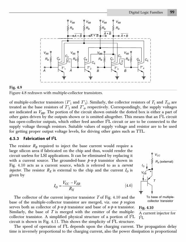
The resistor RB required to inject the base current would require alarge silicon area if fabricated on the chip and thus, would render thecircuit useless for LSI applications. It can be eliminated by replacing itwith a current source. The grounded-base p-n-p transistor shown inFig. 4.10 acts as a current source, which is referred to as a currentinjector. The resistor RX is external to the chip and the current IO isgiven by
EBCCO
X
V VI
R-
= (4.6)
The collector of the current injector transistor T of Fig. 4.10 and thebase of the multiple-collector transistor are merged, viz. one p regionserves both as collector of p-n-p transistor and base of n-p-n transistor.Similarly, the base of T is merged with the emitter of the multiple-collector transistor. A simplified physical structure of a portion of I2Lcircuit is shown in Fig. 4.11. This shows the simplicity of I2L structure.
The speed of operation of I2L depends upon the charging current. The propagation delaytime is inversely proportional to the charging current, also the power dissipation is proportional
VCC
RX (external)
IO
+VEB
T
To base of multiple-
collector transistor
Fig. 4.10A current injector forI2L
A + B� ��
� ��
VBB VBB VBB VBB
RB RB RB RBC4
C2C9
C3C7C8
� �
–
� ��
100 Modern Digital Electronics
to the charging current, therefore we have to trade-off between power dissipation and speed.The figure of merit is independent of IO and it is in the range of 0.1 to 0.7 pJ. The silicon arearequired is very small and packing density in the range 120 to 200 gates per square millimetrehave been realized.
4.6 DIODE–TRANSISTOR LOGIC (DTL)
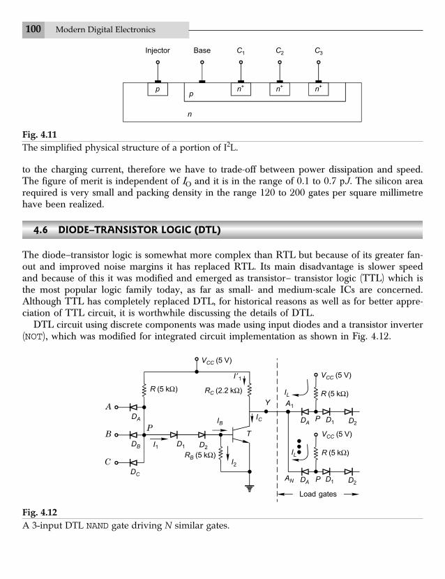
The diode–transistor logic is somewhat more complex than RTL but because of its greater fan-out and improved noise margins it has replaced RTL. Its main disadvantage is slower speedand because of this it was modified and emerged as transistor– transistor logic (TTL) which isthe most popular logic family today, as far as small- and medium-scale ICs are concerned.Although TTL has completely replaced DTL, for historical reasons as well as for better appre-ciation of TTL circuit, it is worthwhile discussing the details of DTL.
DTL circuit using discrete components was made using input diodes and a transistor inverter(NOT), which was modified for integrated circuit implementation as shown in Fig. 4.12.
p
n
Injector Base C1 C2 C3
Fig. 4.11The simplified physical structure of a portion of I2L.
VCC (5 V)
VCC (5 V)
R (5 kW)IL
P D1 D2DA
D2DAAN
IB
D1 D2I1
R (5 kW)
VCC (5 V)
R (5 kW)
ADA
CDC
BDB
P
RC (2.2 kW)
T
IC
I ¢1
RB (5 kW)I2
Y A1
IL
Load gates
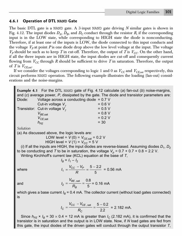
Fig. 4.12A 3-input DTL NAND gate driving N similar gates.
p n+ n+ n+
P D1
Digital Logic Families 101
4.6.1 Operation of DTL NAND Gate
The basic DTL gate is a NAND gate. A 3-input NAND gate driving N similar gates is shown inFig. 4.12. The input diodes DA, DB, and DC conduct through the resistor R, if the correspondinginput is in the LOW state, while corresponding to HIGH state the diode is nonconducting.Therefore, if at least one of the inputs is LOW, the diode connected to this input conducts andthe voltage VP at point P is one diode drop above the low level voltage at the input. The voltageVP should be such as to keep T in cut-off. Therefore, the output of T is VCC. On the other hand,if all the three inputs are in HIGH state, the input diodes are cut-off and consequently currentflowing from VCC through R should be sufficient to drive T in saturation. Therefore, the outputof T is VCE,sat.
If we consider the voltages corresponding to logic 1 and 0 as VCC and VCE,sat respectively, thiscircuit performs NAND operation. The following example illustrates the loading (fan-out) consid-erations and the noise-margins.
Example 4.1 For the DTL NAND gate of Fig. 4.12 calculate (a) fan-out (b) noise-margins,and (c) average power, P, dissipated by the gate. The diode and transistor parameters are:Diode: Voltage across a conducting diode = 0.7 V
Cut-in voltage Vg = 0.6 VTransistor: Cut-in voltage Vg = 0.5 V
VBE,sat = 0.8 VVCE,sat = 0.2 VhFE = 30
Solution(a) As discussed above, the logic levels are:
LOW level = V (0) = VCE,sat = 0.2 VHIGH level = V (1) = VCC = 5 V
(i) If all the inputs are HIGH, the input diodes are reverse-biased. Assuming diodes D1, D2to be conducting and T to be in saturation, the voltage Vp = 0.7 + 0.7 + 0.8 = 2.2 V.
Writing Kirchhoff’s current law (KCL) equation at the base of T,IB = I1 – I2
where I1- -
= =5 2.2
5CC PV V
R = 0.56 mA
and I2 = =,sat 0.8
5BE
B
V
R= 0.16 mA
which gives a base current IB = 0.4 mA. The collector current (without load gates connected)is
IC- -
= =, sat 5 0.2
2.2CC CE
C
V V
R = 2.182 mA.
Since hFE × IB = 30 ¥ 0.4 = 12 mA is greater than IC (2.182 mA), it is confirmed that thetransistor is in saturation and the output is in LOW state. Now, if N load gates are fed fromthis gate, the input diodes of the driven gates will conduct through the output transistor T,

102 Modern Digital Electronics
i.e. T acts as a sink for the current in the input to the gates it drives. Assuming that all theother inputs to each of the load gates are HIGH except the one driven by T, the current
IL- -
= =5 0.9
5CC PV V
R= 0.82 mA. This current is referred to as standard load. The fan-
out is given by IC £ hFE IB, or 0.82 N + 2.182 £ 12 mA or N < 12 since N must be an integer.A conservative choice is N = 10. The Maximum collector current rating of T must be about12 mA.
(ii) If at least one of the inputs is LOW, the corresponding input diode conducts and VP =0.2 + 0.7 = 0.9 V. The minimum voltage required for D1, D2, and T to be conducting is 0.6 +0.6 + 0.5 = 1.7 V, which confirms that D1, D2 are nonconducting and hence T is cut-off.Consequently, the output voltage is VCC (5 V) if the load gates are not connected.If the load gates are connected, the input diodes of the load gates are nonconducting, whichmeans the reverse-saturation current of these diodes must be supplied through the collectorresistor RC , which will produce a voltage drop across RC and consequently the outputvoltage corresponding to HIGH state will be a little less than VCC. The maximum currentwhich can be supplied by the gate will depend upon VOH. The fan-out is determined on thebasis of maximum current.(b) (i) If all the inputs are HIGH, the output is LOW. Since VP = 2.2 V, the input diodes arereverse-biased by 5 – 2.2 = 2.8 V. Since the cut-in voltage of the diode is 0.6 V, a negativenoise spike of at least 3.4 V present at the input will cause malfunction of the circuit, i.e. the0 level noise margin D 0 = 3.4 V.(ii) If at least one input is LOW, the output is HIGH. Since VP = 0.9 V and a voltage of atleast 1.7 V [part a (ii)] is required for D1, D2, and T to conduct, therefore a positive noisespike of at least 0.8 V will cause malfunction of the circuit, i.e. the 1 level noise margin D 1 =0.8 V.(c) The power P(0) when the output is LOW is given by P(0) = VCC (I1 + I¢1) = 5 (0.56 +2.182) = 13.71 mW. When the output is in the HIGH state at least one of the input diodesconduct. Therefore, I1 = 0.82 mA and I¢1 = 0. Hence P(1) = (0.82) (5) = 4.1 mW.
If we assume that the occurrence of LOW and HIGH is equally likely then the averagepower is
Pav+ +
= =( 0 ) (1) 13.71 4.1
2 2P P
= 8.905 mW
4.6.2 Propagation Delays
Delays are associated with the turning-on (turn-on delay) and the turning-off (turn-off delay) of theoutput transistor. While turning on, any capacitance shunting the output of the gate dischargesrapidly through the low impedance of the output transistor in saturation. On the other hand, atturn-off the shunt capacitor must charge through the pull-up resistor RC in addition to thestorage time delay. The turn-off delay is considerably larger than the turn-on delay, often by afactor of 2 or 3. The propagation delay time of commercially available DTL gates are of theorder of 30 to 80 ns.
4.6.3 Current Sink Logic
This gate supplies the reverse-saturation current of input diodes of the load gates in 1 state andsinks the current flowing through the forward-biased input diodes of the load gates in the
Digital Logic Families 103
output transistor of the gate in 0 state. Since the sink current is much greater than the sourcecurrent, this is known as current sink logic.
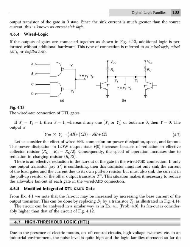
4.6.4 Wired-Logic
If the outputs of gates are connected together as shown in Fig. 4.13, additional logic is per-formed without additional hardware. This type of connection is referred to as wired-logic, wired-AND, or implied-AND.
A
B
C
D
Y1
Y2
Y = Y1 ◊ Y2
VCC
RC
VCC
RC
Y1 Y2
Y = Y1 ◊ Y2
T ¢ T ¢¢
(a) (b)
Fig. 4.13The wired-AND connection of DTL gates
If Y1 = Y2 = 1, then Y = 1, whereas if any one (Y1 or Y2) or both are 0, then Y = 0. Theoutput is
Y = Y1 Y2 ( ) ( )AB CD AB CD= ◊ = + (4.7)
Let us consider the effect of wired-AND connection on power dissipation, speed, and fan-out.The power dissipation in LOW output state P(0) increases because of reduction in effectivecollector resistor (RC || RC = RC/2). Consequently, the speed of operation increases due toreduction in charging resistor (RC/2).
There is an effective reduction in the fan-out of the gate in the wired-AND connection. If onlyone output transistor (say T ¢) is conducting, then this transistor must not only sink the currentof the load gates and the current due to its own pull-up resistor but must also sink the current inthe pull-up resistor of the other output transistor T ¢¢. This situation makes it necessary to reducethe allowable fan-out of each gate in the wired-AND connection.
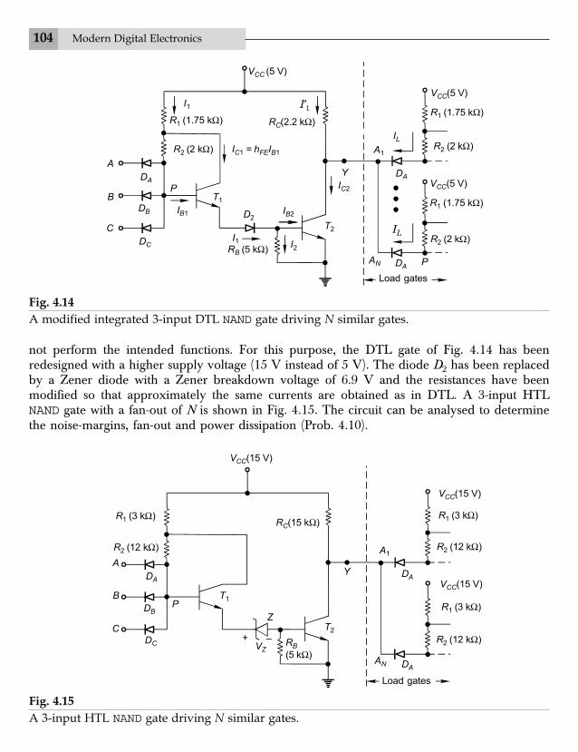
4.6.5 Modified Integrated DTL NAND Gate
From Ex. 4.1 we note that the fan-out may be increased by increasing the base current of theoutput transistor. This can be done by replacing D1 by a transistor T1, as illustrated in Fig. 4.14.
The circuit can be analysed in a similar way as in Ex. 4.1 (Prob. 4.9). Its fan-out is consider-ably higher than that of the circuit of Fig. 4.12.
4.7 HIGH-THRESHOLD LOGIC (HTL)
Due to the presence of electric motors, on–off control circuits, high voltage switches, etc. in anindustrial environment, the noise level is quite high and the logic families discussed so far do
104 Modern Digital Electronics
VCC (5 V)
I¢1RC(2.2 kW)
A
DA
P
R2 (2 kW) R2 (2 kW)
VCC(5 V)
R1 (1.75 kW)
R2 (2 kW)
PAN
IL
IL
T1
VCC(5 V)
R1 (1.75 kW)R1 (1.75 kW)
I1
D2
IC2
Y
IB2
I2
A1
DA
IB1
DC
C
DB
B
DA
I1RB (5 kW)
T2
IC1 = hFEIB1
Fig. 4.14A modified integrated 3-input DTL NAND gate driving N similar gates.
not perform the intended functions. For this purpose, the DTL gate of Fig. 4.14 has beenredesigned with a higher supply voltage (15 V instead of 5 V). The diode D2 has been replacedby a Zener diode with a Zener breakdown voltage of 6.9 V and the resistances have beenmodified so that approximately the same currents are obtained as in DTL. A 3-input HTLNAND gate with a fan-out of N is shown in Fig. 4.15. The circuit can be analysed to determinethe noise-margins, fan-out and power dissipation (Prob. 4.10).
RC(15 kW)
R2 (12 kW)
VCC(15 V)
R1 (3 kW)
R2 (12 kW)
AN
VCC(15 V)
R1 (3 kW)
A1
DA
C
R1 (3 kW)
R2 (12 kW)
A
DA
B
DB
DC
PT1
T2
Z
VZ
+ – RB
(5 kW)
Y
DA
VCC(15 V)
Fig. 4.15A 3-input HTL NAND gate driving N similar gates.
Load gates
Load gates
Digital Logic Families 105
The propagation delay time is adversely affected due to large resistance values. It is as highas hundreds of nano-seconds. The temperature sensitivity of the HTL gate is considerably lessthan that of DTL (Prob. 4.12).
4.8 TRANSISTOR – TRANSISTOR LOGIC (TTL)
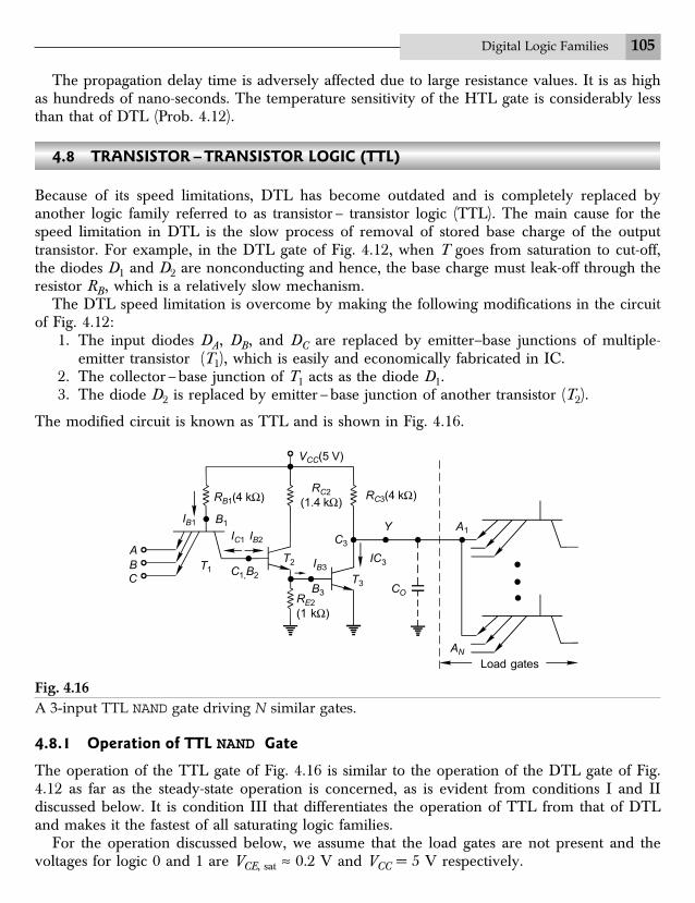
Because of its speed limitations, DTL has become outdated and is completely replaced byanother logic family referred to as transistor – transistor logic (TTL). The main cause for thespeed limitation in DTL is the slow process of removal of stored base charge of the outputtransistor. For example, in the DTL gate of Fig. 4.12, when T goes from saturation to cut-off,the diodes D1 and D2 are nonconducting and hence, the base charge must leak-off through theresistor RB, which is a relatively slow mechanism.
The DTL speed limitation is overcome by making the following modifications in the circuitof Fig. 4.12:
1. The input diodes DA, DB, and DC are replaced by emitter–base junctions of multiple-emitter transistor (T1), which is easily and economically fabricated in IC.
2. The collector – base junction of T1 acts as the diode D1.3. The diode D2 is replaced by emitter – base junction of another transistor (T2).
The modified circuit is known as TTL and is shown in Fig. 4.16.
VCC(5 V)
RB1(4 kW)
IB1 B1
A
B
CT1 C1,B2
IC1 IB2
RE2
(1 kW)
IB3T2
T3
Y A1
C3
IC3
CO
AN
RC3(4 kW)
Load gates
RC2
(1.4 kW)
Fig. 4.16A 3-input TTL NAND gate driving N similar gates.
4.8.1 Operation of TTL NAND Gate
The operation of the TTL gate of Fig. 4.16 is similar to the operation of the DTL gate of Fig.4.12 as far as the steady-state operation is concerned, as is evident from conditions I and IIdiscussed below. It is condition III that differentiates the operation of TTL from that of DTLand makes it the fastest of all saturating logic families.
For the operation discussed below, we assume that the load gates are not present and thevoltages for logic 0 and 1 are VCE, sat ª 0.2 V and VCC = 5 V respectively.
B3
106 Modern Digital Electronics
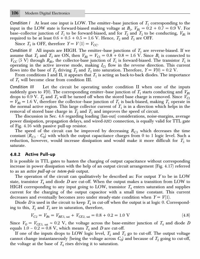
Condition I At least one input is LOW. The emitter–base junction of T1 corresponding to theinput in the LOW state is forward-biased making voltage at B1, VB1 = 0.2 + 0.7 = 0.9 V. Forbase–collector junction of T1 to be forward-biased, and for T2 and T3 to be conducting, VB1 isrequired to be at least 0.6 + 0.5 + 0.5 = 1.6 V. Hence, T2 and T3 are OFF.
Since T3 is OFF, therefore Y = V (1) = VCC .
Condition II All inputs are HIGH. The emitter–base junctions of T1 are reverse-biased. If weassume that T2 and T3 are ON, then VB2 = VC1 = 0.8 + 0.8 = 1.6 V. Since B1 is connected toVCC (5 V) through RB1, the collector-base junction of T1 is forward-biased. The transistor T1 isoperating in the active inverse mode, making IC1 flow in the reverse direction. This currentflows into the base of T2 driving T2 and T3 into saturation. Therefore, Y = V(0) ª 0.2 V.
From conditions I and II, it appears that T1 is acting as back-to-back diodes. The importanceof T1 will become clear from condition III.
Condition III Let the circuit be operating under condition II when one of the inputssuddenly goes to V(0). The corresponding emitter–base junction of T1 starts conducting and VB1drops to 0.9 V. T2 and T3 will be turned off when the stored base charge is removed. Since VC1= VB2 = 1.6 V, therefore the collector–base junction of T1 is back-biased, making T1 operate inthe normal active region. This large collector current of T1 is in a direction which helps in theremoval of stored base charge in T2 and T3 and improves the speed of circuit.
The discussion in Sec. 4.6 regarding loading (fan-out) considerations, noise-margins, averagepower dissipation, propagation delays, and wired-AND connection, is equally valid for TTL gateof Fig. 4.16 with passive pull-up resistor.
The speed of the circuit can be improved by decreasing RC 3 which decreases the timeconstant (RC 3 ◊ CO) with which the output capacitance charges from 0 to 1 logic level. Such areduction, however, would increase dissipation and would make it more difficult for T3 tosaturate.
4.8.2 Active Pull-upIt is possible in TTL gates to hasten the charging of output capacitance without correspondingincrease in power dissipation with the help of an output circuit arrangement (Fig. 4.17) referredto as an active pull-up or totem-pole output.
The operation of the circuit can qualitatively be described as: For output Y to be in LOWstate, transistor T4 and diode D are cut-off. When the output makes a transition from LOW toHIGH corresponding to any input going to LOW, transistor T4 enters saturation and suppliescurrent for the charging of the output capacitor with a small time constant. This currentdecreases and eventually becomes zero under steady-state condition when Y = V (1).
Diode D is used in the circuit to keep T4 in cut-off when the output is at logic 0. Correspond-ing to this, T2 and T3 are in saturation, therefore,
VC 2 = VB4 = VBE 3, sat + VCE 2, sat = 0.8 + 0.2 = 1.0 V (4.8)
Since VO = VCE 3, sat ª 0.2 V, the voltage across the base-emitter junction of T4 and diode Dequals 1.0 – 0.2 = 0.8 V, which means T4 and D are cut-off.
If one of the inputs drops to LOW logic level, T2 and T3 go to cut-off. The output voltagecannot change instantaneously (being the voltage across CO) and because of T2 going to cut-off,the voltage at the base of T4 rises driving it to saturation.
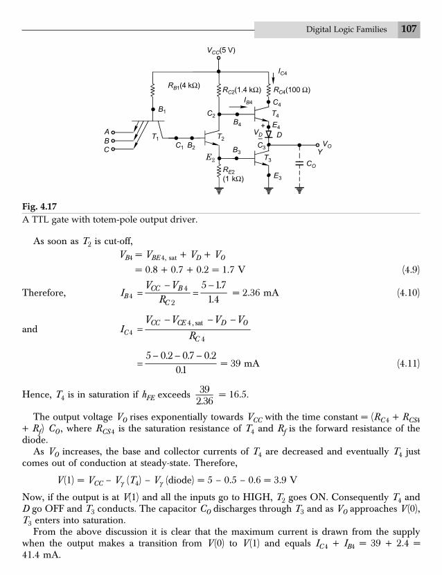
Digital Logic Families 107
As soon as T2 is cut-off,VB4 = VBE 4, sat + VD + VO
= 0.8 + 0.7 + 0.2 = 1.7 V (4.9)
Therefore, IB 44
2
5 1.71.4
BCC
C
V VR
- -= = = 2.36 mA (4.10)
and IC 44 , sat
4
DCC CE O
C
V V V V
R
- - -=
5 0.2 0.7 0.20.1
- - -= = 39 mA (4.11)
Hence, T4 is in saturation if hFE exceeds 392.36
= 16.5.
The output voltage VO rises exponentially towards VCC with the time constant = (RC 4 + RCS4+ Rf ) CO , where RCS 4 is the saturation resistance of T4 and Rf is the forward resistance of thediode.
As VO increases, the base and collector currents of T4 are decreased and eventually T4 justcomes out of conduction at steady-state. Therefore,
V (1) = VCC – Vg (T4) – Vg (diode) = 5 – 0.5 – 0.6 = 3.9 V
Now, if the output is at V(1) and all the inputs go to HIGH, T2 goes ON. Consequently T4 andD go OFF and T3 conducts. The capacitor CO discharges through T3 and as VO approaches V (0),T3 enters into saturation.
From the above discussion it is clear that the maximum current is drawn from the supplywhen the output makes a transition from V (0) to V (1) and equals IC 4 + IB4 = 39 + 2.4 =41.4 mA.
RB1(4 kW)RC2(1.4 kW) RC4(100 W)
B1
A
B
C
T1
C1 B2
T2
C2
T3
RE2
(1 kW)
B3
IC4
C4
B4 +
E2
∑CO
YVO
E4
T4
VCC(5 V)
IB4
Fig. 4.17A TTL gate with totem-pole output driver.
–VD
C3∑
E3
D

108 Modern Digital Electronics
This current spike generates noise in the power supply distribution system and increasespower dissipation in the gate, more so when it is operated at high frequencies.
4.8.3 Wired-AND
Wired-AND connection must not be used for totem-pole output circuits because of the currentspike problem discussed above (Prob. 4.16). TTL circuits with open-collector outputs are avail-able which can be used for wired-AND connections.
4.8.4 Open-Collector Output
A circuit with open-collector output is same as the circuit of Fig. 4.16 except for the collector –resistor RC3 of T3 which is missing. The collector terminal C3 is available outside the IC and thepassive pull-up is to be connected externally. Naturally, the advantages of active pull-up are notavailable in this. Gates with open-collector output can be used for wired-AND operation (Prob.4.18).
4.8.5 Unconnected Inputs
If any input of a TTL gate is left disconnected (open orfloating) the corresponding E–B junction of T1 will not beforward-biased. Hence, it acts exactly in the same way asif a logical 1 is applied to that input. Therefore, in TTLICs, all unconnected inputs are treated as logical 1s. How-ever, the unused inputs should either be connected tosome used input(s) or returned to VCC through a resistor.
4.8.6 Clamping Diodes
Clamping diodes are commonly used in all TTL gates tosuppress the ringing caused from the fast voltage transi-tions found in TTL. These diodes shown in Fig. 4.18 clampthe negative undershoot at approximately – 0.7 V.
4.9 SCHOTTKY TTL
The speed limitation of TTL is mainly due to the turn-off time delays involved in transistorswhile making transitions from saturation to cut-off. This can be eliminated by replacing thetransistors of TTL gate by Schottky transistors.
With this, the transistors are prevented from entering saturation and hence, there is saving inturn-off time. Schottky TTL gates have propagation delay time of the order of 2 ns which isvery small in comparison with the propagation delay time of standard TTL which is of theorder of 10 ns. It is a nonsaturating bipolar logic.
4.10 5400/7400 TTL SERIES
TTL 5400/7400 series is the most popular and commonly used series of digital ICs. 7400devices are used for commercial applications whereas the 5400 devices are used for military
A
B
C
T1
Clamping
diodes
Fig. 4.18A portion of a TTL gate showingthe clamping diodes.
Digital Logic Families 109
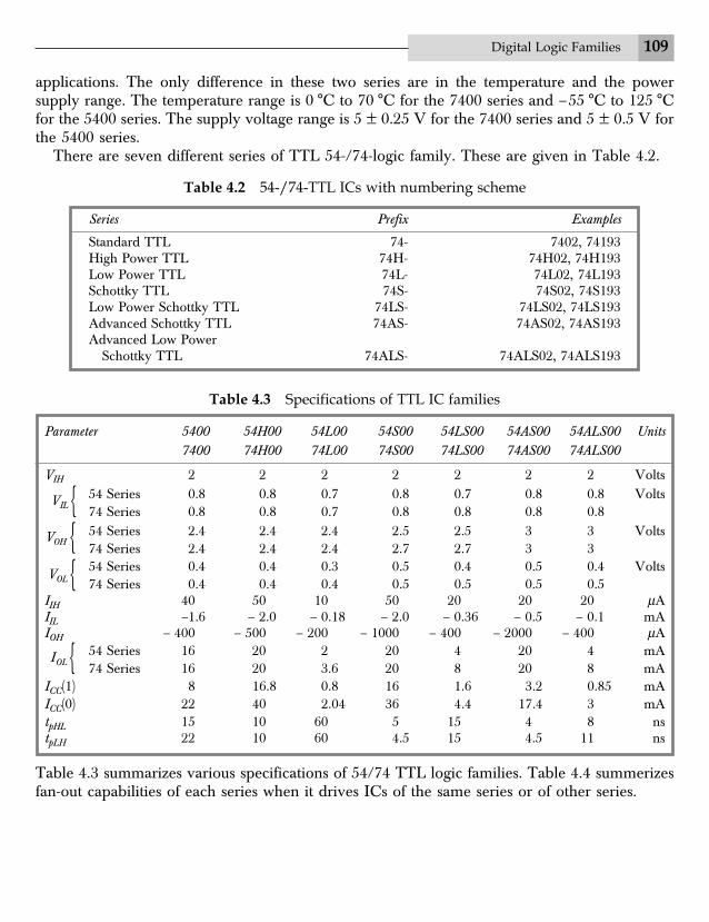
applications. The only difference in these two series are in the temperature and the powersupply range. The temperature range is 0 °C to 70 °C for the 7400 series and –55 °C to 125 °Cfor the 5400 series. The supply voltage range is 5 ± 0.25 V for the 7400 series and 5 ± 0.5 V forthe 5400 series.
There are seven different series of TTL 54-/74-logic family. These are given in Table 4.2.
Table 4.2 54-/74-TTL ICs with numbering scheme
Series Prefix Examples
Standard TTL 74- 7402, 74193High Power TTL 74H- 74H02, 74H193Low Power TTL 74L- 74L02, 74L193Schottky TTL 74S- 74S02, 74S193Low Power Schottky TTL 74LS- 74LS02, 74LS193Advanced Schottky TTL 74AS- 74AS02, 74AS193Advanced Low Power
Schottky TTL 74ALS- 74ALS02, 74ALS193
Table 4.3 Specifications of TTL IC families
Parameter 5400 54H00 54L00 54S00 54LS00 54AS00 54ALS00 Units7400 74H00 74L00 74S00 74LS00 74AS00 74ALS00
VIH 2 2 2 2 2 2 2 Volts
{ILV 54 Series 0.8 0.8 0.7 0.8 0.7 0.8 0.8 Volts74 Series 0.8 0.8 0.7 0.8 0.8 0.8 0.8
{OHV 54 Series 2.4 2.4 2.4 2.5 2.5 3 3 Volts74 Series 2.4 2.4 2.4 2.7 2.7 3 3
{OLV 54 Series 0.4 0.4 0.3 0.5 0.4 0.5 0.4 Volts74 Series 0.4 0.4 0.4 0.5 0.5 0.5 0.5
IIH 40 50 10 50 20 20 20 mAIIL –1.6 – 2.0 – 0.18 – 2.0 – 0.36 – 0.5 – 0.1 mAIOH – 400 – 500 – 200 – 1000 – 400 – 2000 – 400 mA
{OLI 54 Series 16 20 2 20 4 20 4 mA74 Series 16 20 3.6 20 8 20 8 mA
ICC(1) 8 16.8 0.8 16 1.6 3.2 0.85 mAICC(0) 22 40 2.04 36 4.4 17.4 3 mAtpHL 15 10 60 5 15 4 8 nstpLH 22 10 60 4.5 15 4.5 11 ns
Table 4.3 summarizes various specifications of 54/74 TTL logic families. Table 4.4 summerizesfan-out capabilities of each series when it drives ICs of the same series or of other series.

110 Modern Digital Electronics
Table 4.4 Summary of TTL fan-out capabilities
Source TTLdevice
Load TTLdevice Æ
Ø 54/ 54H/ 54L/ 54S/ 54LS/ 54AS/ 54ALS/74 74H 74L 74S 74LS 74AS 74ALS
54/74 10 8 40 8 20 20 2054H/74H 12 10 50 10 25 25 2554L/74L 2 1 20 1 10 7 1054S/74S 12 10 100 10 50 40 5054LS/74LS 5 4 40 4 20 16 2654AS/74AS 12 10 110 10 55 40 10054ALS/74ALS 5 4 40 4 20 16 20
From Table 4.3, we observe the following:
(i) The input and output voltage specifications are compatible for each of the TTL series,which makes it possible to use any mix of ICs of these series to achieve optimum designfrom the point of view of propagation delay and power dissipation.
(ii) The input and output current specifications are compatible and the number of gates ofeach of the series, which can be safely driven from any series can be determined as givenin Table 4.4.
(iii) The low power dissipation series L, LS, and ALS have minimum power requirement andare suitable for battery operated circuits. Out of these series ALS series has the minimumpropagation delay and therefore it is fast replacing other series.
(iv) H series has low propagation delay (high speed) but requires maximum power.(v) S and AS series have very low propagation delay. The AS series is fast replacing S series
because of its lower dissipation and propagation delay.
4.11 EMITTER-COUPLED LOGIC (ECL)
Emitter-coupled logic (ECL) is the fastest of all logic families and therefore is used in applica-tions where very high speed is essential. High speeds have become possible in ECL because thetransistors are used in difference amplifier configuration, in which they are never driven intosaturation and thereby the storage time is eliminated. Here, rather than switching the transistorsfrom ON to OFF and vice-versa, they are switched between cut-off and active regions. Propa-gation delays of less than 1 ns per gate have become possible in ECL.
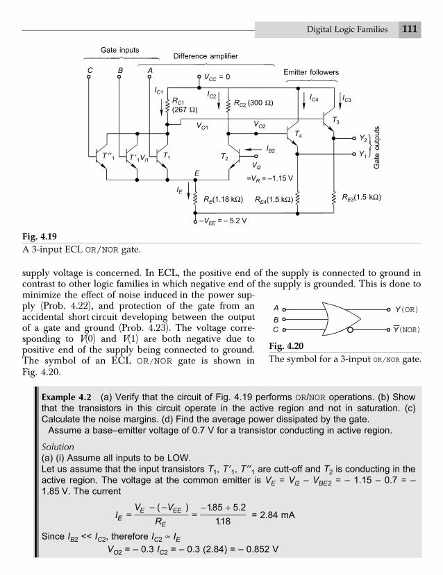
Basically, ECL is realized using difference amplifier in which the emitters of the two transis-tors are connected and hence it is referred to as emitter-coupled logic. A 3-input ECL gate isshown in Fig. 4.19, which has three parts: The middle part is the difference amplifier whichperforms the logic operation.
Emitter follower are used for d.c. level shifting of the outputs, so that V(0) and V(1) are samefor the inputs and the outputs. Note that two output Y1 and Y2 are available in this circuit whichare complementary. Y1 corresponds to OR logic and Y2 to NOR logic and hence it is named asan OR/NOR gate.
Additional transistors are used in parallel to T1 to get the required fan-in. There is a funda-mental difference between all other logic families (including MOS logic) and ECL as far as the
Digital Logic Families 111
supply voltage is concerned. In ECL, the positive end of the supply is connected to ground incontrast to other logic families in which negative end of the supply is grounded. This is done tominimize the effect of noise induced in the power sup-ply (Prob. 4.22), and protection of the gate from anaccidental short circuit developing between the outputof a gate and ground (Prob. 4.23). The voltage corre-sponding to V(0) and V(1) are both negative due topositive end of the supply being connected to ground.The symbol of an ECL OR/NOR gate is shown inFig. 4.20.
Example 4.2 (a) Verify that the circuit of Fig. 4.19 performs OR/NOR operations. (b) Showthat the transistors in this circuit operate in the active region and not in saturation. (c)Calculate the noise margins. (d) Find the average power dissipated by the gate.
Assume a base–emitter voltage of 0.7 V for a transistor conducting in active region.
Solution(a) (i) Assume all inputs to be LOW.Let us assume that the input transistors T1, T ¢1, T ¢¢1 are cutt-off and T2 is conducting in theactive region. The voltage at the common emitter is VE = Vi2 – VBE2 = – 1.15 – 0.7 = –1.85 V. The current
IE- - - +
= =( ) 1.85 5.2
1.18E EE
E
V VR
= 2.84 mA
Since IB2 << IC2, therefore IC2 ª IEVO2 = – 0.3 IC2 = – 0.3 (2.84) = – 0.852 V
ABC
Difference amplifier
VCC = 0
IC1 IC2RC1
(267 W)RC2 (300 W)
IC4 IC3
T1 T2
T4
T3
T ¢¢1 T ¢1Vi1
IB2
Vi2
=VR = –1.15 V
RE4(1.5 kW)
IE
E
Emitter followers
Y2
Y1
RE3(1.5 kW)
–VEE = – 5.2 V
Gate inputs
VO1VO2
Fig. 4.19A 3-input ECL OR/NOR gate.
Fig. 4.20The symbol for a 3-input OR/NOR gate.
A
B
C
Y(OR)
Y(NOR)
¸˝˛
Gate
outp
uts
RE(1.18 kW)

112 Modern Digital Electronics
Transistor T4 will be conducting and the output at Y1 = VO2 – VBE4 = – 0.852 – 0.7 =– 1.55 V which is assumed to be V(0).
Therefore, if all the inputs are at V(0) = –1.55 V, then the base-to-emitter voltage of theinput transistor is
VBE = Vi1 – VE = – 1.55 + 1.85 = 0.3 Vwhich is less than the cut-in voltage (0.5 V) of the transistor and hence the input transistorsare non-conducting, as was assumed above.
The base and collector of T3 are effectively at the same potential, hence T3 behaves as adiode. The current flowing through this diode is approximately 3 mA which corresponds to avoltage of about 0.75 V across the diode. Therefore, the voltage at Y2 = – 0.75 V which isassumed to be V(1). This shows that Y1 and Y2 are complementary, i.e. Y2 = 1Y .(ii) Assume at least one input to be HIGH. Corresponding to this the input transistor T1 isassumed to be conducting and T2 to be cut-off.Then VE = Vi1 – VBE1 = –0.75 – 0.7 = – 1.45 VHence, VBE2 = Vi2 – VE = –1.15 + 1.45 = 0.3 V which verifies the assumption that T2 iscut-of.The voltage VO1 = –RC1 × IC1
where IC1- -
=( )E EE
E
V VR
- +=
( 1.45 5.2 )1.18 = 3.18 mA
Since the collector current of T1 is higher than the collector current of T2 when it is conduct-ing, hence RC1 < RC2 to get the same voltage levels.
This gives voltage at Y2 = –1.55 = V(0). The voltage at Y1 = – 0.75 = V(1). From (i) and (ii)above, we see that OR function is performed at Y1 and NOR at Y2. Hence it is an OR/NORgate. Its voltages corresponding to logic 0 and 1 are –1.55 V and – 0.75 V respectively. Thelogic swing is 0.8 V.
(b) From part (a) (i), the voltage between collector and base of T2 is VCB2 = VO2 – Vi2 =– 0.85 + 1.15 = 0.30 V which shows that the C–B junction is reverse-biased and hence T2 isoperating in its active region.
From part (a) (ii), the voltage between the collector and base of T1 isVCB1 = VO1 – Vi1 = – 0.85 + 0.75 = –0.1 V
This shows that the C–B junction of T1 is forward-biased but its magnitude is much lessthan the cut-in voltage and hence T1 is operating in its active region.(c) From part (a)(i), the base–emitter voltage of the input transistors is 0.3 V which is 0.2 Vless than the cut-in voltage. Hence the noise margin D 0 = 0.2 V.From part (a) (ii) the base-emitter voltage of T2 is 0.3 V which again gives a noise marginD1 = 0.2 V. The noise margins are equal and are quite small. (d) From part (a) (i),
IC2 = 2.84 mA

Digital Logic Families 113
IC3-
=5.2 0.75
1.5= 2.97 mA
and IC4-
=5.2 1.55
1.5= 2.43 mA
From part (a) (ii),IC1 = 3.18 mAIC3 = 2.43 mAIC4 = 2.97 mA
Therefore, average IE = +2.84 3.182
= 3.01 mA. The total power supply current drain
IEE = 3.01 + 2.97 + 2.43 = 8.41 mATherefore, the power dissipation = VEE · IEE = (5.2) (8.41)
= 43.7 mW
4.11.1 Fan-Out
If all the inputs are LOW, the input transistors are cut-off. Therefore the input resistance is veryhigh. On the other hand, if an input is HIGH, the input resistance is that of an emitter followerwhich is also high. Therefore, the input impedance is always high.
The output resistance is either that of an emitter follower or the forward resistance of a diode(T3 or T4 acts as a diode) which is always low. Because of the low output impedance and highinput impedance, the fan-out is large.
4.11.2 Wired-OR Logic
The outputs of two or more ECL gates can be connected to obtain additional logic withoutusing additional hardware. The wired-OR configurations are shown in Fig. 4.21.
A
B
C
Y1
Y1
Y1 + Y2 Y1 + Y2
Y2
Y2
G2
G1
D
E
A
B
C
G2
G1
E
Y1
Y1
Y1 + Y2
Y2
D
(a) (b)
Fig. 4.21Wired-OR connection of ECL gates.
Y2
Y1 + Y2

114 Modern Digital Electronics
4.11.3 Open-Emitter OutputsSimilar to open-collector output in TTL, open-emitter outputs are available in ECL which isuseful for wired-OR applications.
4.11.4 Unconnected InputsIf any input of an ECL gate is left unconnected, the corresponding E-B junction of the inputtransistor will not be conducting. Hence it acts as if a logical 0 level voltage is applied to thatinput. Therefore, in ECL ICs, all unconnected inputs are treated as logical 0s.
4.11.5 ECL FamiliesThere are two popular ECL families:10xxx (or 10K) series and 100xxx (or 100K) series. The100K series is the fastest of all logic families and has a propagation delay time less than 1 ns.Their voltage specifications are given in Table 4.5.
Table 4.5 Voltage specifications of ECL seriesSeries Supply voltage VOL VOH VIL VIH
VEE , V V V V V
10K 5.2 –1.7 –0.9 –1.4 –1.2100K 4.5 –1.7 –0.9 –1.4 –1.2
4.12 INTERFACING ECL AND TTL
It is often necessary to mix logic circuits of different families in the design of a digital system torealize the speed and power requirements by choosing the appropriate logic families for differ-ent parts of the system. Consider the interfacing between TTL and ECL gates. The logic levelsin the two systems are entirely different and there-fore level shifting circuits are required to be inter-posed between TTL and ECL gates. For TTL-to-ECL and ECL-to-TTL interfacing two level trans-lator ICs are available. Interfacing using these ICsare described below.
4.12.1 TTL-to-ECL Translator
The MC10H124 is a quad TTL-to-ECL translatorIC. It is a 16-pin IC and its logic diagram is shownin Fig. 4.22. It uses two power supplies; one posi-tive and another negative for the generation ofproper logic levels for ECL and TTL.
The logic levels of the translator circuit are:VIH = 2V, VIL = 0.8 VVOH = –0.98V, VOL = –1.63V
Ai
GND
Fig. 4.22Logic diagram of MC10H124 TTL-to-ECLtranslator
VCC (+5V) VEE (–5.2V)
Commonstorbe
�o
Ao
�o
Bo
�o
Co
�o
Do
Bi
Ci
Di
Digital Logic Families 115
From Table 4.3, we haveVOH = 2.4 V and VOL = 0.4 V for TTL ICs. Comparing the output logic levels of TTL and
the input logic levels of the translator IC, we observe,VIH (Translator) < VOH (TTL)
and VIL (Translator) > VOL(TTL)which shows that the input logic levels of the translator are compatible with the output logiclevels of TTL.
Similarly, comparing the output logic levels of the translator with the input logic levels ofECL (Table 4.5), we obtain
VIH (ECL) < VOH (Translator)and VIL (ECL) > VOL (Translator)which demonstrates that the output logic levels of the translator are compatible with the inputlogic levels of ECL.
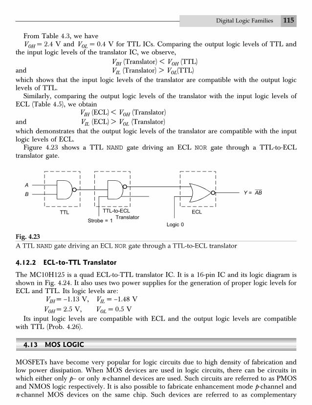
Figure 4.23 shows a TTL NAND gate driving an ECL NOR gate through a TTL-to-ECLtranslator gate.
TTL TTL-to-ECL ECL
Y = ��
Strobe = 1Translator
Logic 0
Fig. 4.23A TTL NAND gate driving an ECL NOR gate through a TTL-to-ECL translator
4.12.2 ECL-to-TTL Translator
The MC10H125 is a quad ECL-to-TTL translator IC. It is a 16-pin IC and its logic diagram isshown in Fig. 4.24. It also uses two power supplies for the generation of proper logic levels forECL and TTL. Its logic levels are:
VIH = –1.13 V, VIL = –1.48 VVOH = 2.5 V, VOL = 0.5 V
Its input logic levels are compatible with ECL and the output logic levels are compatiblewith TTL (Prob. 4.26).
4.13 MOS LOGIC
MOSFETs have become very popular for logic circuits due to high density of fabrication andlow power dissipation. When MOS devices are used in logic circuits, there can be circuits inwhich either only p– or only n-channel devices are used. Such circuits are referred to as PMOSand NMOS logic respectively. It is also possible to fabricate enhancement mode p-channel andn-channel MOS devices on the same chip. Such devices are referred to as complementary
A
B

116 Modern Digital Electronics
MOSFETs and logic based on these devices is known as CMOS logic. The power dissipation isextremely small for CMOS and hence CMOS logic has become very popular.
The basic MOS gate is an inverter as shown in Fig. 4.25, in which T1 is an enhancementMOSFET which acts as driver and T2 may be an enhancement (Fig. 4.25a) or depletion(Fig. 4.25b) MOSFET, which acts as load. Instead of fabricating diffusion resistor for load,
VCC (+5 V) VEE (–5.2 V)
�i
Ai
�i
Bi
�i
Ci
�i
Di
GND
Ao
Bo
Co
Do
Fig. 4.24Logic diagram of MC10H125 ECL-to-T T L translator
+VDD
T2 (Load)T2 (Load)
+VDD
Vi
+
–
+
–
T1(Driver)
VO
(a) (b)
Vi
+
–
T1(Driver)
+
VO
–
Fig. 4.25A MOS inverter with (a) Enhancement load (b) Depletion load.
Digital Logic Families 117
which usually occupies an area about 20 times that of a MOS device, MOSFET itself is used asthe load. This makes possible high density of fabrication and therefore MOS logic made largescale integration possible.
The logic levels for the MOS circuits areV (0) ª 0V (1) ª VDD
Although the MOS logic circuits are identical in configuration to bipolar DCTL, the prob-lem of current hogging is not present. The operation of MOSFET switches is given in Section3.7.
MOS logic is mainly used for LSI and VLSI ICs and not for SSI and MSI ICs. Most of themicroprocessors, memories, and peripheral devices are available in NMOS.
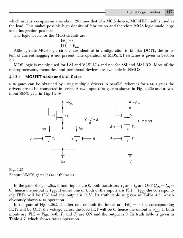
4.13.1 MOSFET NAND and NOR Gates
NOR gates can be obtained by using multiple drivers in parallel, whereas for NAND gates thedrivers are to be connected in series. A two-input NOR gate is shown in Fig. 4.26a and a two-input NAND gate in Fig. 4.26b.
+VDD +VDD
T3
Y = A + B
ID1 ID2
A BT2T1
(a) (b)
A
B
T3
T2
T1
Y = AB
Fig. 4.262-input NMOS gates (a) NOR (b) NAND.
In the gate of Fig. 4.26a, if both inputs are 0, both transistors T1 and T2 are OFF (ID1 = ID2 =0), hence the output is VDD. If either one or both of the inputs are V(1) = VDD , the correspond-ing FETs will be ON and the output is 0 V. Its truth table is given in Table 4.6, whichobviously shows NOR operation.
In the gate of Fig. 4.26b, if either one or both the inputs are V (0) = 0, the correspondingFETs will be OFF, the voltage across the load FET will be 0, hence the output is VDD . If bothinputs are V (1) = VDD , both T1 and T2 are ON and the output is 0. Its truth table is given inTable 4.7, which shows NAND operation.
118 Modern Digital Electronics
Table 4.6 Truth table of Fig. 4.26a
Inputs OutputA B Y
0 0 VDD0 VDD 0
VDD 0 0VDD VDD 0
Table 4.7 Truth table of Fig. 4.26b
Inputs OutputA B Y
0 0 VDD0 VDD VDD
VDD 0 VDDVDD VDD 0
4.13.2 Fan-Out
Since MOS devices have very high input impedance, therefore, the fan-out is large. But drivinga large number of MOS gates increases the capacitance at the output of the driving gate whichreduces, considerably, the speed of MOS gates.
The voltage and current parameters for 8085, 8086 microprocessors and other NMOSdevices are:
VCC = 5 VVIL = 0.8 VVIH = 2 VVOL = 0.45 V, IOL = 2 mAVOH = 2.4 V, IOH = –400 mA
The input and output leakage currents are ± 10 mA.These voltages are directly compatible with TTL ICs. Usually, NMOS devices are available
with higher sink currents which are directly compatible with TTL ICs. This helps in easyinterfacing between NMOS devices and TTL devices.
4.13.3 Propagation Delay Time
The propagation delay time is large in MOS devices because of large capacitances present atthe input and output of these devices. Also, the resistance through which these capacitors getcharged and discharged is high.
In MOS devices, the phenomenon of minority charge storage is not present, and the speedof operation is mainly determined by the speed with which the capacitors get charged anddischarged.
Due to the developments in the technology of MOS fabrication, it has become possible toobtain speeds which are comparable to TTL.

Digital Logic Families 119
4.13.4 Power Dissipation
In the NAND gate of Fig. 4.26b, current is drawn from the power supply only during one of thefour possible input conditions, whereas in the NOR gate of Fig. 4.23a power is drawn duringthree out of four input conditions. Therefore, the power consumption in MOS circuits is smallwhich is very useful for large-scale integration.
4.13.5 Unconnected Inputs
MOS devices have very high input impedance and even a very small static charge flowing intothis high impedance can develop a dangerously high voltage. This may cause damage to thedevice by rupturing the insulation layer and also to the persons handling such devices. There-fore, MOS ICs inputs must not be left unconnected. Even for storage of such devices, conduc-tive foam or aluminium foil should be used which will ensure shorting of IC pins together sothat no voltage can be developed between the pins. Necessary precautions must be taken whilehandling such devices.
4.14 CMOS LOGIC
A complementary MOSFET (CMOS) is obtained by connecting a p-channel and an n-channelMOSFET in series, with drains tied together and the output is taken at the common drain.Input is applied at the common gate formed by connecting the two gates together (Fig. 3.33). ina CMOS, p-channel and n-channel enhancement MOS devices are fabricated on the same chip,which makes its fabrication more complicated and reduces the packing density. But because ofnegligibly small power consumption, CMOS is ideally suited for battery operated systems.
Its speed is limited by substrate capacitances. To reduce the effect of these substrate capaci-tances, the latest technology known as silicon on sapphire (SOS) is used in microprocessorfabrication which employs an insulating substrate (sapphire). CMOS has become the mostpopular in MSI and LSI areas and is the only possible logic for the fabrication of VLSI devices.
4.14.1 CMOS Inverter
The basic CMOS logic circuit is an inverter shown in Fig. 3.33. For this circuit the logic levelsare 0 V (logic 0) and VCC (logic 1). When Vi = VCC , T1 turns ON and T2 turns OFF. ThereforeVO ª 0 V, and since the transistors are connected in series the current ID is very small. On theother hand, when Vi = 0 V, T1 turns OFF and T2 turns ON giving an output voltage VO ª VCCand ID is again very small. In either logic state, T1 or T2 is OFF and the quiscent powerdissipation which is the product of the OFF leakage current and VCC is very low. More complexfunctions can be realized by combinations of inverters.
4.14.2 CMOS NAND and NOR Gates
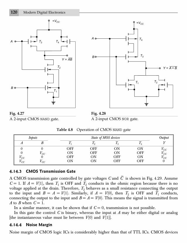
A 2-input CMOS NAND gate is shown in Fig. 4.27 and NOR gate in Fig. 4.28. In the NAND gate,the NMOS drivers are connected in series, where as the PMOS loads are connected in parallel.On the other hand, the CMOS NOR gate is obtained by connecting the NMOS drivers inparallel and PMOS loads in series. The operation of NAND gate can be understood from Table4.8. The operation of the NOR gate can be verified in the similar manner (Prob. 4.29).
120 Modern Digital Electronics
Table 4.8 Operation of CMOS NAND gate
Inputs State of MOS devices OutputA B T1 T2 T3 T4 Y
0 0 OFF OFF ON ON VCC0 VCC ON OFF ON OFF VCC
VCC 0 OFF ON OFF ON VCCVCC VCC ON ON OFF OFF 0
4.14.3 CMOS Transmission Gate
A CMOS transmission gate controlled by gate voltages C and C is shown in Fig. 4.29. AssumeC = 1. If A = V (1), then T1 is OFF and T2 conducts in the ohmic region because there is novoltage applied at the drain. Therefore, T2 behaves as a small resistance connecting the outputto the input and B = A = V (1). Similarly, if A = V (0), then T2 is OFF and T1 conducts,connecting the output to the input and B = A = V (0). This means the signal is transmitted fromA to B when C = 1.
In a similar manner, it can be shown that if C = 0, transmission is not possible.In this gate the control C is binary, whereas the input at A may be either digital or analog
[the instantaneous value must lie between V (0) and V(1)].
4.14.4 Noise Margin
Noise margin of CMOS logic ICs is considerably higher than that of TTL ICs. CMOS devices
Y = AB
A T3 T4
T1
+VCC
T2
Fig. 4.27A 2-input CMOS NAND gate.
Fig. 4.28A 2-input CMOS NOR gate.
+VCC
T4
T3
T1T2
Y = A + B
A
B
B

Digital Logic Families 121
have wide supply voltage range and the noise margin increases with the supply voltage VCC .Typically, it is 0.45 VCC .
4.14.5 Unconnected Inputs
The unconnected CMOS ICs inputs behave in a way similar to MOS devices discussed inSection 4.13. Therefore, the unused inputs must be connected to either the supply voltageterminal or one of the used inputs provided that the fan-out of the signal source is not ex-ceeded. This is highly unlikely for CMOS circuits because of their high fan-out.
Some CMOS ICs have Zener diodes connected at the inputs for protection against highinput voltages.
4.14.6 Wired-Logic
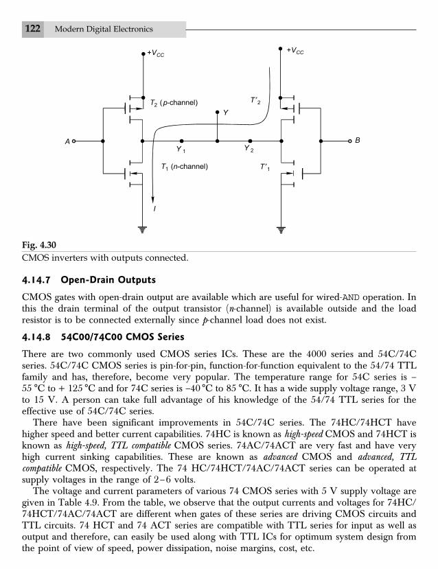
Figure 4.30 shows two CMOS inverters with their outputs connected together. In this circuit,(i) When A = B = V (0)
T1 and T¢1 are cut-off and Y = V (1) = VCC
(ii) When A = B = V (1)T1 and T¢1 are ON and Y = V (0) = 0
(iii) When A = V(1) and B = V (0)T1 and T¢2 are ON whereasT1¢ and T2 are OFF
Therefore, a large current I will flow as shown in Fig. 4.30.This will make voltage at Y equal to VCC/2 which is neither in the range of logic 0 nor in therange of logic 1. Therefore, the circuit will not operate properly. Also because of large currentI, the transistors will be damaged.
Similarly, corresponding to A = V (0) and B = V (1) the operation will not be proper.Therefore, wired-logic must not be used for CMOS logic circuits.
S2 D2
G2
T2 (PMOS)
T1 (NMOS)
A B
S1 D1
G1
C
(a) (b)
BA
C
TG
Fig. 4.29(a) A CMOS transmission gate (b) Its symbol.
C C
122 Modern Digital Electronics
4.14.7 Open-Drain Outputs
CMOS gates with open-drain output are available which are useful for wired-AND operation. Inthis the drain terminal of the output transistor (n-channel) is available outside and the loadresistor is to be connected externally since p-channel load does not exist.
4.14.8 54C00/74C00 CMOS Series
There are two commonly used CMOS series ICs. These are the 4000 series and 54C/74Cseries. 54C/74C CMOS series is pin-for-pin, function-for-function equivalent to the 54/74 TTLfamily and has, therefore, become very popular. The temperature range for 54C series is –55 °C to + 125 °C and for 74C series is –40 °C to 85 °C. It has a wide supply voltage range, 3 Vto 15 V. A person can take full advantage of his knowledge of the 54/74 TTL series for theeffective use of 54C/74C series.
There have been significant improvements in 54C/74C series. The 74HC/74HCT havehigher speed and better current capabilities. 74HC is known as high-speed CMOS and 74HCT isknown as high-speed, TTL compatible CMOS series. 74AC/74ACT are very fast and have veryhigh current sinking capabilities. These are known as advanced CMOS and advanced, TTLcompatible CMOS, respectively. The 74 HC/74HCT/74AC/74ACT series can be operated atsupply voltages in the range of 2–6 volts.
The voltage and current parameters of various 74 CMOS series with 5 V supply voltage aregiven in Table 4.9. From the table, we observe that the output currents and voltages for 74HC/74HCT/74AC/74ACT are different when gates of these series are driving CMOS circuits andTTL circuits. 74 HCT and 74 ACT series are compatible with TTL series for input as well asoutput and therefore, can easily be used along with TTL ICs for optimum system design fromthe point of view of speed, power dissipation, noise margins, cost, etc.
A
I
T ¢1
Y 1
T ¢2
B
T1 (n-channel)
Y 2
+VCC
Fig. 4.30CMOS inverters with outputs connected.
Y
T2 (p-channel)
+VCC
Digital Logic Families 123
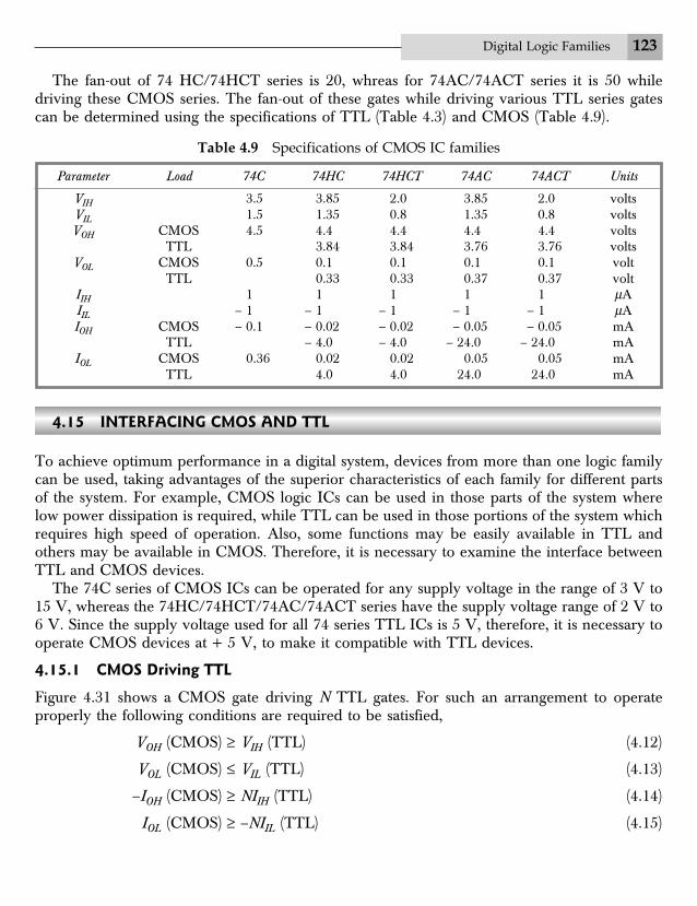
The fan-out of 74 HC/74HCT series is 20, whreas for 74AC/74ACT series it is 50 whiledriving these CMOS series. The fan-out of these gates while driving various TTL series gatescan be determined using the specifications of TTL (Table 4.3) and CMOS (Table 4.9).
Table 4.9 Specifications of CMOS IC families
Parameter Load 74C 74HC 74HCT 74AC 74ACT Units
VIH 3.5 3.85 2.0 3.85 2.0 voltsVIL 1.5 1.35 0.8 1.35 0.8 voltsVOH CMOS 4.5 4.4 4.4 4.4 4.4 volts
TTL 3.84 3.84 3.76 3.76 voltsVOL CMOS 0.5 0.1 0.1 0.1 0.1 volt
TTL 0.33 0.33 0.37 0.37 voltIIH 1 1 1 1 1 mAIIL – 1 – 1 – 1 – 1 – 1 mAIOH CMOS – 0.1 – 0.02 – 0.02 – 0.05 – 0.05 mA
TTL – 4.0 – 4.0 – 24.0 – 24.0 mAIOL CMOS 0.36 0.02 0.02 0.05 0.05 mA
TTL 4.0 4.0 24.0 24.0 mA
4.15 INTERFACING CMOS AND TTL
To achieve optimum performance in a digital system, devices from more than one logic familycan be used, taking advantages of the superior characteristics of each family for different partsof the system. For example, CMOS logic ICs can be used in those parts of the system wherelow power dissipation is required, while TTL can be used in those portions of the system whichrequires high speed of operation. Also, some functions may be easily available in TTL andothers may be available in CMOS. Therefore, it is necessary to examine the interface betweenTTL and CMOS devices.
The 74C series of CMOS ICs can be operated for any supply voltage in the range of 3 V to15 V, whereas the 74HC/74HCT/74AC/74ACT series have the supply voltage range of 2 V to6 V. Since the supply voltage used for all 74 series TTL ICs is 5 V, therefore, it is necessary tooperate CMOS devices at + 5 V, to make it compatible with TTL devices.
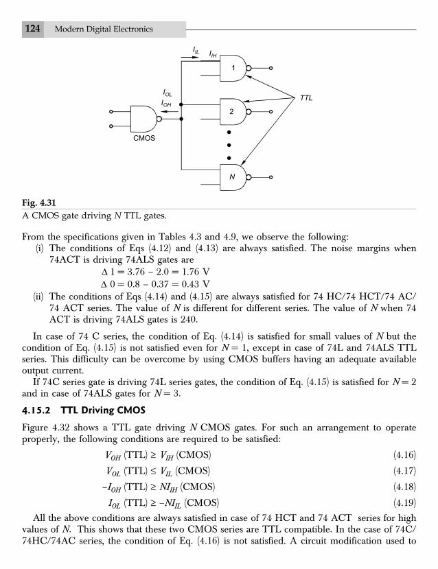
4.15.1 CMOS Driving TTL
Figure 4.31 shows a CMOS gate driving N TTL gates. For such an arrangement to operateproperly the following conditions are required to be satisfied,
VOH (CMOS) ≥ VIH (TTL) (4.12)
VOL (CMOS) £ VIL (TTL) (4.13)
–IOH (CMOS) ≥ NIIH (TTL) (4.14)
IOL (CMOS) ≥ –NIIL (TTL) (4.15)
124 Modern Digital Electronics
From the specifications given in Tables 4.3 and 4.9, we observe the following:(i) The conditions of Eqs (4.12) and (4.13) are always satisfied. The noise margins when
74ACT is driving 74ALS gates areD 1 = 3.76 – 2.0 = 1.76 VD 0 = 0.8 – 0.37 = 0.43 V
(ii) The conditions of Eqs (4.14) and (4.15) are always satisfied for 74 HC/74 HCT/74 AC/74 ACT series. The value of N is different for different series. The value of N when 74ACT is driving 74ALS gates is 240.
In case of 74 C series, the condition of Eq. (4.14) is satisfied for small values of N but thecondition of Eq. (4.15) is not satisfied even for N = 1, except in case of 74L and 74ALS TTLseries. This difficulty can be overcome by using CMOS buffers having an adequate availableoutput current.
If 74C series gate is driving 74L series gates, the condition of Eq. (4.15) is satisfied for N = 2and in case of 74ALS gates for N = 3.
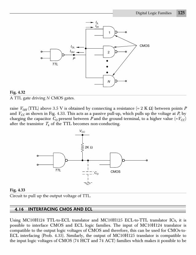
4.15.2 TTL Driving CMOS
Figure 4.32 shows a TTL gate driving N CMOS gates. For such an arrangement to operateproperly, the following conditions are required to be satisfied:
VOH (TTL) ≥ VIH (CMOS) (4.16)
VOL (TTL) £ VIL (CMOS) (4.17)
–IOH (TTL) ≥ NIIH (CMOS) (4.18)
IOL (TTL) ≥ –NIIL (CMOS) (4.19)
All the above conditions are always satisfied in case of 74 HCT and 74 ACT series for highvalues of N. This shows that these two CMOS series are TTL compatible. In the case of 74C/74HC/74AC series, the condition of Eq. (4.16) is not satisfied. A circuit modification used to
IOL
IOH
CMOS
N
2
TTL
1
IIL IIH
Fig. 4.31A CMOS gate driving N TTL gates.
Digital Logic Families 125
raise VOH (TTL) above 3.5 V is obtained by connecting a resistance (ª 2 K W) between points Pand VCC as shown in Fig. 4.33. This acts as a passive pull-up, which pulls up the voltage at P, bycharging the capacitor CO present between P and the ground terminal, to a higher value (ªVCC )after the transistor T4 of the TTL becomes non-conducting.
N
2
1
IOL
IOH
CMOS
TTL
P
IIH
IIL
Fig. 4.32A TTL gate driving N CMOS gates.
VCC
2K W
CMOS
Fig. 4.33Circuit to pull up the output voltage of TTL.
4.16 INTERFACING CMOS AND ECL
Using MC10H124 TTL-to-ECL translator and MC10H125 ECL-to-TTL translator ICs, it ispossible to interface CMOS and ECL logic families. The input of MC10H124 translator iscompatible to the output logic voltages of CMOS and therefore, this can be used for CMOs-to-ECL interfacing (Prob. 4.33). Similarly, the output of MC10H125 translator is compatible tothe input logic voltages of CMOS (74 HCT and 74 ACT) families which makes it possible to be
CO
TTL
126 Modern Digital Electronics
used it for ECL-to-CMOS interfacing. Other CMOS logic families can also be interfaced usingpull-up resistor similar to Fig. 4.33 (Prob. 4.34).
4.17 TRI-STATE LOGIC
In normal logic circuits there are two states of the output, LOW and HIGH. If the output is notin the LOW state, it is definitely in the other state (HIGH). Similarly, if the output is not in theHIGH state, it is definitely in the LOW state. In complex digital systems like microcomputersand microprocessors, a number of gate outputs may be required to be connected to a commonline which is referred to as a bus which, in turn, may be required to drive a number of gateinputs. When a number of gate outputs are connected to the bus, we encounter some difficul-ties. These are:
1. Totem-pole outputs cannot be connected together because of very large current drainfrom the supply and consequent heating of the ICs which may get damaged.
2. Open-collector outputs can be connected together with a common collector-resistorconnected externally. This causes the problems of loading and speed of operation.
To overcome these difficulties, special circuits have been developed in which there is onemore state of the output, referred to as the third state or high-impedance state, in addition to theLOW and HIGH states. These circuits are known as TRI-STATE, tri-state logic (TSL) or three-state logic. TRI-STATE, is a registered trade mark of National Semiconductor Corporation ofUSA.
There is a basic functional difference between wired-OR and the TSL. For the wired-ORconnection of two functions Y1 and Y2 is
Y = Y1 + Y2 (4.20)whereas for TSL, the result is not a Boolean function but an ability to multiplex many functionseconomically.
4.17.1 TSL Inverter
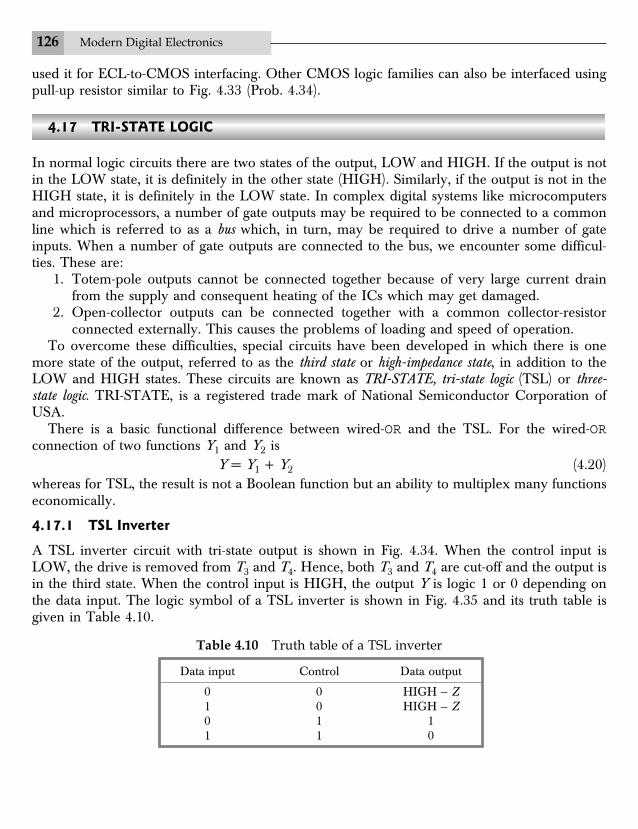
A TSL inverter circuit with tri-state output is shown in Fig. 4.34. When the control input isLOW, the drive is removed from T3 and T4. Hence, both T3 and T4 are cut-off and the output isin the third state. When the control input is HIGH, the output Y is logic 1 or 0 depending onthe data input. The logic symbol of a TSL inverter is shown in Fig. 4.35 and its truth table isgiven in Table 4.10.
Table 4.10 Truth table of a TSL inverter
Data input Control Data output
0 0 HIGH — Z1 0 HIGH — Z0 1 11 1 0
Digital Logic Families 127
T1
+VCC
YData output
T4
T3
Data outputData input
Control
Fig. 4.34A TSL inverter.
Fig. 4.35Logic symbol of a TSL inverter.
The output and input current specifications of TSL family are given in Table 4.11.
Table 4.11 Current specifications of TSL family
Parameter Control input
LOW (DISABLE) HIGH (ENABLE)
IIH 40 mA 40 mAIIL – 1.6 mA – 1.6 mAIOH 40 mA – 5.2 mAIOL – 40 mA 16 mA
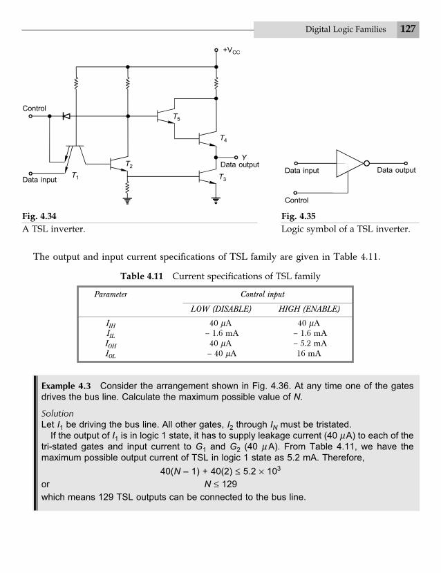
Example 4.3 Consider the arrangement shown in Fig. 4.36. At any time one of the gatesdrives the bus line. Calculate the maximum possible value of N.
SolutionLet I1 be driving the bus line. All other gates, I2 through IN must be tristated.
If the output of I1 is in logic 1 state, it has to supply leakage current (40 mA) to each of thetri-stated gates and input current to G1 and G2 (40 m A). From Table 4.11, we have themaximum possible output current of TSL in logic 1 state as 5.2 mA. Therefore,
40(N – 1) + 40(2) £ 5.2 ¥ 103
or N £ 129which means 129 TSL outputs can be connected to the bus line.
ControlT5
T2
Data input

128 Modern Digital Electronics
4.18 SUMMARY
Essential features of all the major logic families have been discussed and the important conclu-sion are given below:
1. RTL and DTL families are no more used for new systems because of their low speed,high power dissipation, and low fan-out.
2. TTL is the most popular general purpose logic family. It is available in seven differentseries with a wide range of operating speed, power dissipation, and fan-out. There are alarge number of functions in SSI and MSI available in TTL.
TTL ICs are available with totem-pole output (which decreases speed-power prod-uct), open-collector output (which makes possible wired-AND connection and bus opera-tion), and tri-state (TSL) outputs (which are ideally suited for bus operation).
3. HTL are best suited for an industrial environment where electrical noise level is high.4. ECL is the fastest logic family. Its main disadvantages are low noise-margins and high
power dissipation. For interfacing with other logic families, level-shifting networks arerequired.
5. I2L is the only saturated bipolar logic suitable for LSI because of small silicon chip arearequired, and low power consumption. The supply voltage required is low hence it ishighly suitable for battery operated systems.
I2
I1
IN
G1
G2
Bus line
Fig. 4.36N TSL gates driving a bus line.

Digital Logic Families 129
I2L circuits can drive TTL circuits if a resistive load is connected to the output stage ofI2L with a higher supply voltage (5 V).
6. MOS devices occupy a very small fraction of silicon chip area in comparison to bipolardevices and require very small power. Therefore, MOS logic is the most popular logicfor LSI. The main drawback of MOS logic is slow speed, which is being improved uponby improvements in the technology of MOS fabrication. HMOS, a variety of NMOS hasspeeds comparable to bipolar logic families.
7. CMOS has the lowest speed power product and requires very small power.It is the most popular logic family and has led to the VLSI chips.
8. Corresponding to TTL 54/74 series, 54C/74C, 54HC/74HC, 54HCT/74HCT,54AC/74AC and 54ACT/74ACT series have been developed which are directly com-patible with various 54/74TTL series and have the same numbering scheme and pin-outs.
A comparison of various digital IC logic families is given in Table 4.12.
GGGGGlossary
Active pull-up A circuit with active devices used to pull up the output voltage of a logic circuitfrom LOW to HIGH in response to the appropriate inputs.Bipolar logic Logic circuits using bipolar junction semiconductor devices.Breadth of logic family The number of different types of gates and other functions available inan IC logic family.Buffer A circuit or gate that can drive a substantially higher number of gates or other loads.Also known as Buffer driver.Bus A group of conductors carrying a related set of signals.CMOS (Complementary metal-oxide semiconductor) A MOS device that uses one p-channel onen-channel device to make an inverter circuit.Current sink logic A logic circuit in which the output sink current corresponding to logic 0 stateis appreciably higher than the output source current corresponding to logic 1 state.Current source logic A logic circuit in which the output source current corresponding to logic 1state is appreciably higher than the output sink current corresponding to logic 0 state.DCTL (Direct-coupled transistor logic) A form of bipolar logic that uses direct coupling.Depletion mode MOSFET A MOS device in which channel width gets depleted when thevoltage of proper polarity is applied at the gate.DTL (Diode transistor logic) A form of bipolar logic circuit that uses diodes and bipolarjunction transistors to realize a logic operation.ECL (Emitter-coupled logic) A form of bipolar logic circuit that uses emitter-coupled configura-tion.Enhancement mode MOSFET A MOS device in which the channel is formed only when aproper voltage is applied at the gate. The channel width enhances with the increased voltage atthe gate.Fan-in The number of inputs of a logic gate.
130 Modern Digital Electronics

Digital Logic Families 131
132 Modern Digital Electronics
Fan-out The maximum number of similar logic gates which can be driven by a logic gate.Field-effect transistor (FET) A three terminal semiconductor device in which the current flowis due to the flow of one type of charge carriers only. The current in the channel is controlledby the field produced due to the applied voltage at the gate.Figure of merit (of digital ICs) It is the product of speed expressed as propagation delay timeand power dissipation. It is also known as the speed power product.High-impedance state The third state of a tristate logic (TSL) in which the device is inactive andis effectively disconnected from the circuit.HTL (High-threshold logic) A form of bipolar logic circuit which is identical to DTL but hasappreciably higher noise margins.I 2L (Integrated-injection logic) A form of bipolar logic circuit that uses only bipolar transistors.It is an alternative form of DCTL.Logic Swing The difference between the voltages corresponding to HIGH and LOW levels.LSI (Large-scale integration) An IC chip containing logic circuits equivalent of 100 to 1000gates or containing 1000 –10,000 transistors.MOSFET (Metal-oxide-semiconductor field-effect transistor) A field-effect transistor consistingof a semiconductor substrate over which an oxide layer is grown and above the oxide layer ametalic layer is deposited which acts as the gate. If is also known as the insulated-gate FET(IGFET).Merged-transistor logic (MTL) Same as the I2L.MSI (Medium-scale integration) An IC chip containing logic circuits equivalent of 13 to 99gates or containing 100–1000 transistors.Noise immunity A circuits ability to tolerate noise.Noise margin A measure of the noise which can be tolerated by a logic circuit.Noise-margin, high-level For a logic circuit, the difference between the minimum voltage that isproduced at the output corresponding to logic 1 and the minimum voltage that is recognised aslogic 1 of the input.Noise-margin, low-level For a logic circuit the difference between the maximum voltage that isrecognised as logic 0 at the input and the maximum voltage that is produced corresponding tologic 0 at the output.Non-saturated logic A logic circuit in which the BJTs are not driven to saturation correspondingto ON state.Open-collector output An output of a digital IC which is the collector terminal of a BJT notconnected to any other point inside the IC.Open-drain output An output of a MOS IC which is the drain terminal of a MOS device notconnected to any other point in the IC.Open-emitter output An output of an ECL IC which is the emitter terminal of a BJT notconnected to any other point in the IC.Passive pull-up A resistance used to pull-up the output voltage of a logic circuit from LOW toHIGH in response to appropriate inputs.

Digital Logic Families 133
Pull-up resistor A resistor connected between the output (collector or drain of a transistor) andthe supply voltage (VCC or VDD).Saturated logic A logic circuit in which the BJTs are driven to saturation corresponding to ONstate.Schottky TTL The TTL circuit in which each BJT is replaced by a Schottky transistor.SSI (small-scale integration) An IC chip containing circuits equivalent of upto 12 gates or 100transistors.Three-state gate (tristate gate) A gate having a 1, 0, or high-impedance output states.Tristate output An output of a logic circuit having 1, 0, or high-impedance states.Totem-pole output Same as the active pull-up.TSL (Tristate logic) Same as tristate output.TTL (Transistor-transistor logic) A form of bipolar logic circuit that uses transistors to realizethe logic operations.Unipolar logic Logic circuits using only MOS devices.VLSI (Very large-scale integration) An IC chip containing logic circuits equivalent of above1000 gates or above 10,000 transistors.Wire-ANDing Tying the outputs of two or more gates together to perform additional logic. Alsoknown as Wired-Logic.
RRRRReview Questions
4.1 A logic family using BJTs is known as logic family.
4.2 A unipolar logic family uses only devices.
4.3 Figure of merit of a digital IC is given by .
4.4 The number of similar gates which a gate can drive is known as its .
4.5 Fan-in signifies the of a gate.
4.6 A TTL gate is driving another TTL gate. The output transistor of the driver gate is driven into saturation when its output is at low level.
4.7 For interfacing logic gates VOH must be than VIH.
4.8 Outputs of TTL gates with active pull-up must connected together.
4.9 Unconnected input terminal of a TTL gate behaves as .
4.10 The input terminal of a CMOS circuit must .
4.11 Schottky TTL has propagation delay time than TTL.
4.12 The temperature range for 74-series ICs is .
4.13 The states of a TSL are .
4.14 TTL gates with output can be used for wired-logic operation.
4.15 is the fastest logic family.

134 Modern Digital Electronics
PPPPProblems
4.1 In the RTL NOR gate of Fig. 4.4, calculate the average power supplied by VCC to the driver gatewhen it is driving 5 gates. Assume VBE, sat ª 0.8 V, VCE, sat ª 0.2 V, hFE = 10. Neglect leakagecurrents.
4.2 In the circuit of Fig. 4.4, calculate(a) Output voltage VO and noise margin D 1 for N = 5, 6, 7, 8, 9, 10. Assume hFE = 10.(b) Repeat (a) for hFE = 20.(c) Comment on the effect of hFE on the fan-out and noise margin of circuit.(d) Comment on the effect of N on the noise margin for a given hFE.
4.3 In the circuit of Fig. 4.6, the fan-out of RTL NOR gates P and Q is 5 each.(a) Calculate the fan-out of the combined gate.(b) Evaluate the propagation delay time constant and power dissipation, and comment on the
effect of wired-logic on these.
4.4 A buffer is used to increase the output drive capability of a logic circuit. An RTL buffer inverter isshown in Fig. 4.37.(a) Explain the operation of this circuit.(b) Calculate the fan-out. Assume hFE = 30.(c) Consider outputs of two such buffers A and B connected in parallel. Let the input to buffer A
be logic 1 and the input to buffer B be logic 0. Calculate the current flowing in T3 of buffer A.
640 W
450 W
450 W
450 W
100 W
450 W
450 W
T2
G1
I1
GNT3
IN
VO
Buffer inverter Load gates
IOT1
VCC = 3.6 V
Fig. 4.37An RTL buffer inverter driving N RTL gates.
4.5 What will happen in the DTL circuit of Fig. 4.12 if(a) one of the diodes D1 or D2 is removed,(b) one more diode D3 is inserted in series with D1 and D2.
4.6 Calculate the value of hFE required for a fan-out of 10 in the DTL gate of Fig. 4.12.
Ii
Vi

Digital Logic Families 135
4.7 M DTL gates (Fig 4.12) each with a fan-out of N are connected in a wired-AND connection.Determine the fan-out of this combination as a function of number M.
4.8 In the modified DTL NAND gate of Fig. 4.14, show that when T1 is conducting it is in its activeregion and not in the saturation region.
4.9 Explain the operation of the modified DTL gate of Fig. 4.14 and calculate its (a) fan-out (b) noise-margins, and (c) average power dissipation. Assume hFE = 30.
4.10 Calculate (a) noise-margins, (b) fan-out, and (c) power dissipation of HTL gate of Fig. 4.15. AssumehFE = 40.
4.11 Repeat Problem 4.7 for the HTL gate shown in Fig. 4.15.
4.12 Explain why the temperature sensitivity of HTL is significantly better than that of DTL.
4.13 In the TTL NAND gate of Fig. 4.17 determine the current drawn from the supply, when the output(a) is LOW(b) is HIGH(c) makes a transition from LOW to HIGH.
4.14 Consider the circuit shown in Fig. 4.38 which uses TTL gates. The current I is 1.6 mA whenterminal B is left unconnected. Find the value of I when B is connected to A. Comment on the effectof this connection on the fan-out of gate G1.
G1G2
IA
BLogic 1
Fig. 4.38Circuit for Problem 4.14.
Fig. 4.39Circuit for Problem 4.16.
T4T4
D
Y1 Y2
T3 T3
DY
4.15 In the TTL gate of Fig. 4.17, what happens if(a) RC4 = 0,(b) diode D is not present,(c) the output accidently gets shorted to ground?
4.16 The outputs of two totem-pole TTL gates (Fig. 4.17)are connected as shown in Fig. 4.39. Obtain the cur-rent drawn from the supply for all the possible combi-nations of the inputs to the two gates.
4.17 For an open-collector TTL gate, the specifications are:VOH = 2.4 VVOL = 0.4 VIOH = 250 mAIOL = 16 mAIIH = 40 mAIIL = –1.6 mA
Calculate the value of RC required for the open-collector gate. Assume VCC = 5 V and a fan-outof 8.
4.18 If 5 open-collector gates of Problem 4.17 are wire-ANDed, and are loaded by similar 6 gates,calculate the value of collector resistor RC required.
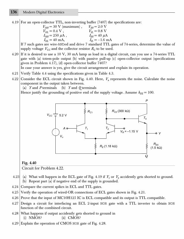
136 Modern Digital Electronics
4.19 For an open-collector TTL, non-inverting buffer (7407) the specifications are:VOH = 30 V (maximum) , VIH = 2.0 VVOL = 0.4 V , VIL = 0.8 VIOH = 250 mA , IIH = 40 mAIOL = 40 mA, IIL = –1.6 mA
If 7 such gates are wire-ANDed and drive 7 standard TTL gates of 74-series, determine the value ofsupply voltage VCC and the collector resistor RC to be used.
4.20 If it is desired to use a 10 V, 30 mA lamp as load in a digital circuit, can you use a 74-series TTLgate with (a) totem-pole output (b) with passive pull-up (c) open-collector output (specificationsgiven in Problem 4.17), (d) open-collector buffer 7407?In case your answer is yes, give the circuit arrangement and explain its operation.
4.21 Verify Table 4.4 using the specifications given in Table 4.3.
4.22 Consider the ECL circuit shown in Fig. 4.40. Here, Vn represents the noise. Calculate the noisecomponent in the output taken between.(a) Y and P terminals (b) Y and Q terminals
Hence justify the grounding of positive end of the supply voltage. Assume hFE = 100.
P
T4
Y
T2T1
Vn
RC1
5.2 VVCC
AVR = –1.15 V
RE (1.18 kW)
Q
RC2 (300 kW)
RE4
(1.5 kW)
Fig. 4.40Circuit for Problem 4.22.
4.23 (a) What will happen in the ECL gate of Fig. 4.19 if Y1 or Y2 accidently gets shorted to ground.(b) Repeat part (a) if negative end of the supply is grounded.
4.24 Compare the current spikes in ECL and TTL gates.
4.25 Verify the operation of wired-OR connections of ECL gates shown in Fig. 4.21.
4.26 Prove that the input of MC10H125 IC is ECL compatible and its output is TTL compatible.
4.27 Design a circuit for interfacing an ECL 2-input NOR gate with a TTL inverter to obtain NORfunction of the combined circuit.
4.28 What happens if output accidently gets shorted to ground in(i) NMOS? (ii) CMOS?
4.29 Explain the operation of CMOS NOR gate of Fig. 4.28.
Digital Logic Families 137
4.30 Find the fan-out of each of the 74 TTL series driving 74 HC/74 HCT/74 AC/74 ACT gates usingthe specifications given in Tables 4.3 and 4.9.
4.31 Consider a CMOS gate driving TTL gates. Find the fan-out when(a) 74HC/74HCT gate is driving each of TTL series gates.(b) 74AC/74ACT gate is driving each of TTL series gates.
4.32 A 74AC/74ACT gate is driving twenty 74AS gates. It is desired to drive some 74ALS gates inaddition to this. Find the maximum possible number of 74ALS gates which can be connected.
4.33 Is it possible to use TTL-to-ECL translator for CMOS-to-ECL interfacing? Justify your answer.
4.34 Is it possible to use ECL-to-TTL translator for ECL-to-CMOS interfacing? Justify your answer.