Embed Size (px)
Citation preview
8/6/2019 Introduction Digital Logic
http://slidepdf.com/reader/full/introduction-digital-logic 1/22
1
Introduction to Digital Logic Design
Appendix A of CO&A
Dr. Farag
8/6/2019 Introduction Digital Logic
http://slidepdf.com/reader/full/introduction-digital-logic 2/22
2
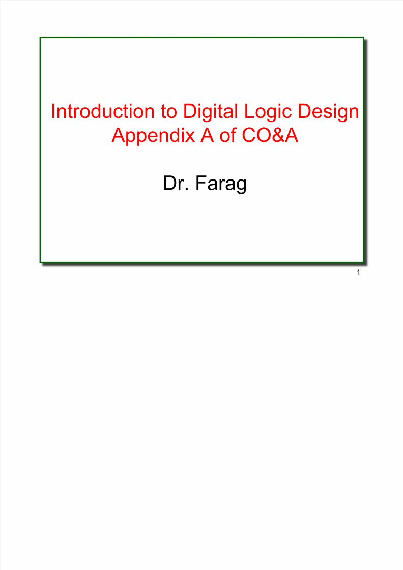
• Boolean Algebra
• Gates
• Combinational Circuits – Simplifications of Boolean Functions
– Multiplexers, Decoders, PLA, ROM, Adders
• Sequential Circuits – Flip-Flops
– Registers
– Counters
Outline
8/6/2019 Introduction Digital Logic
http://slidepdf.com/reader/full/introduction-digital-logic 3/22
3
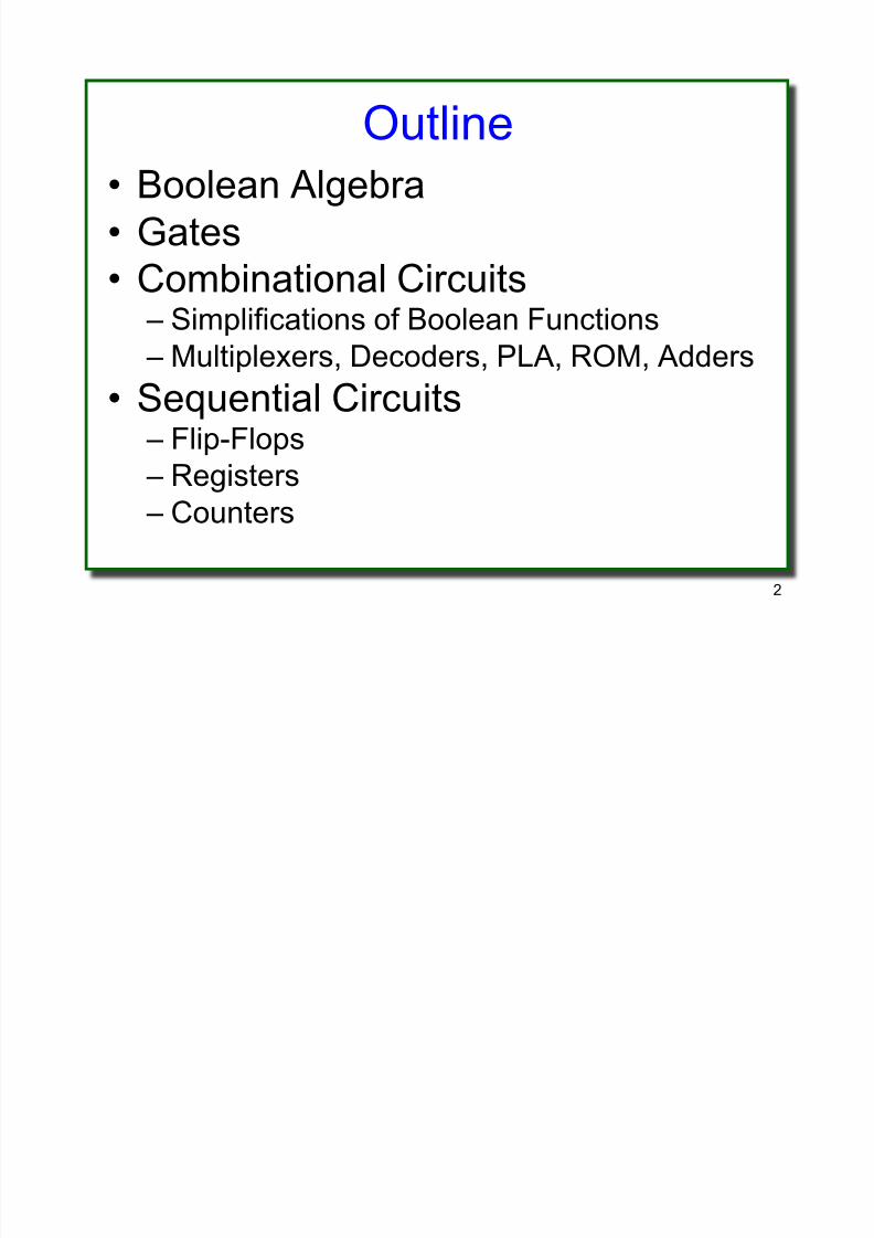
• Similar to traditional algebra but it defines a set of logical operations and variables
• Basic operations: AND, OR, NOT (., +, _
)
• These operations are defined by their truth tables
•
Other operations can be derived from the basic ones.Ex: NAND, NOR, XOR, XNOR
Boolean Algebra
8/6/2019 Introduction Digital Logic
http://slidepdf.com/reader/full/introduction-digital-logic 4/22
4
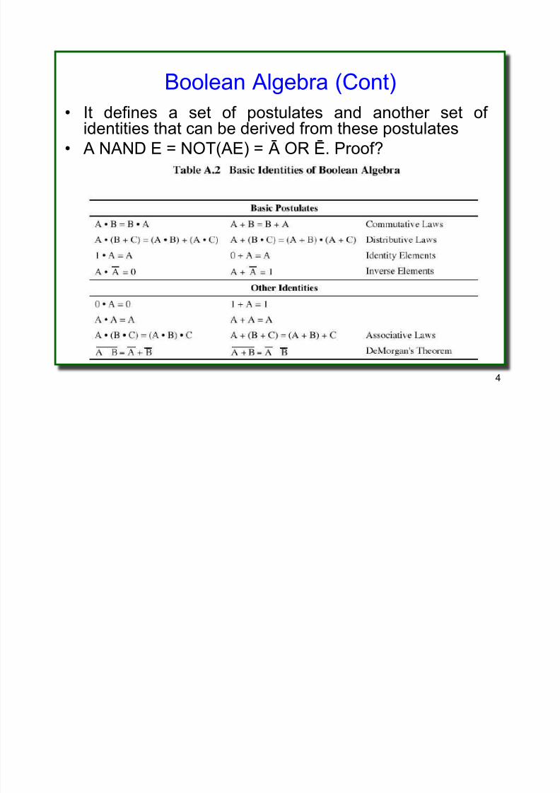
• It defines a set of postulates and another set of identities that can be derived from these postulates
• A NAND E = NOT(AE) = Ā OR Ē. Proof?
Boolean Algebra (Cont)
8/6/2019 Introduction Digital Logic
http://slidepdf.com/reader/full/introduction-digital-logic 5/22
5
• To implement any logic function we need a functionallycomplete set of gates. Ex (AND, OR, NOT), (AND,NOT), (OR, NOT) (NAND), (NOR)
• How to implement all basic functions by NAND??Examine its truth table. Same for NOR
• From manufacturing point of view, using only one typeof gates to implement the circuit is very advantageous.Why? Regular -> Simple -> easy to design -> cheap
• Gates are the basic building blocks of all digitalsystems. They are implemented using electronicscomponents (transistors, diodes, resistors, etc.)
• Different families are TTL, CMOS, ECL, etc. Not our problem
Gates
8/6/2019 Introduction Digital Logic
http://slidepdf.com/reader/full/introduction-digital-logic 6/22
6
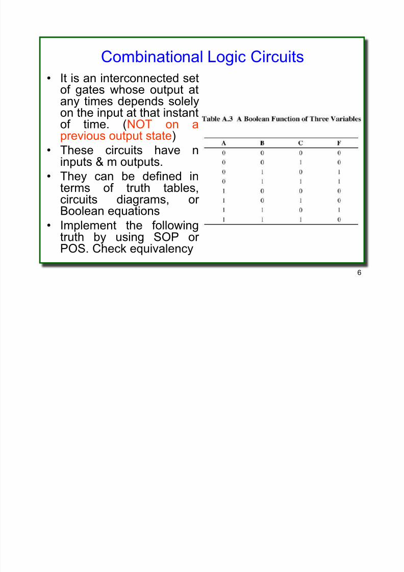
Combinational Logic Circuits
• It is an interconnected setof gates whose output atany times depends solelyon the input at that instantof time. (NOT on a
previous output state)• These circuits have ninputs & m outputs.
• They can be defined interms of truth tables,circuits diagrams, or
Boolean equations• Implement the following
truth by using SOP or POS. Check equivalency
8/6/2019 Introduction Digital Logic
http://slidepdf.com/reader/full/introduction-digital-logic 7/22
7
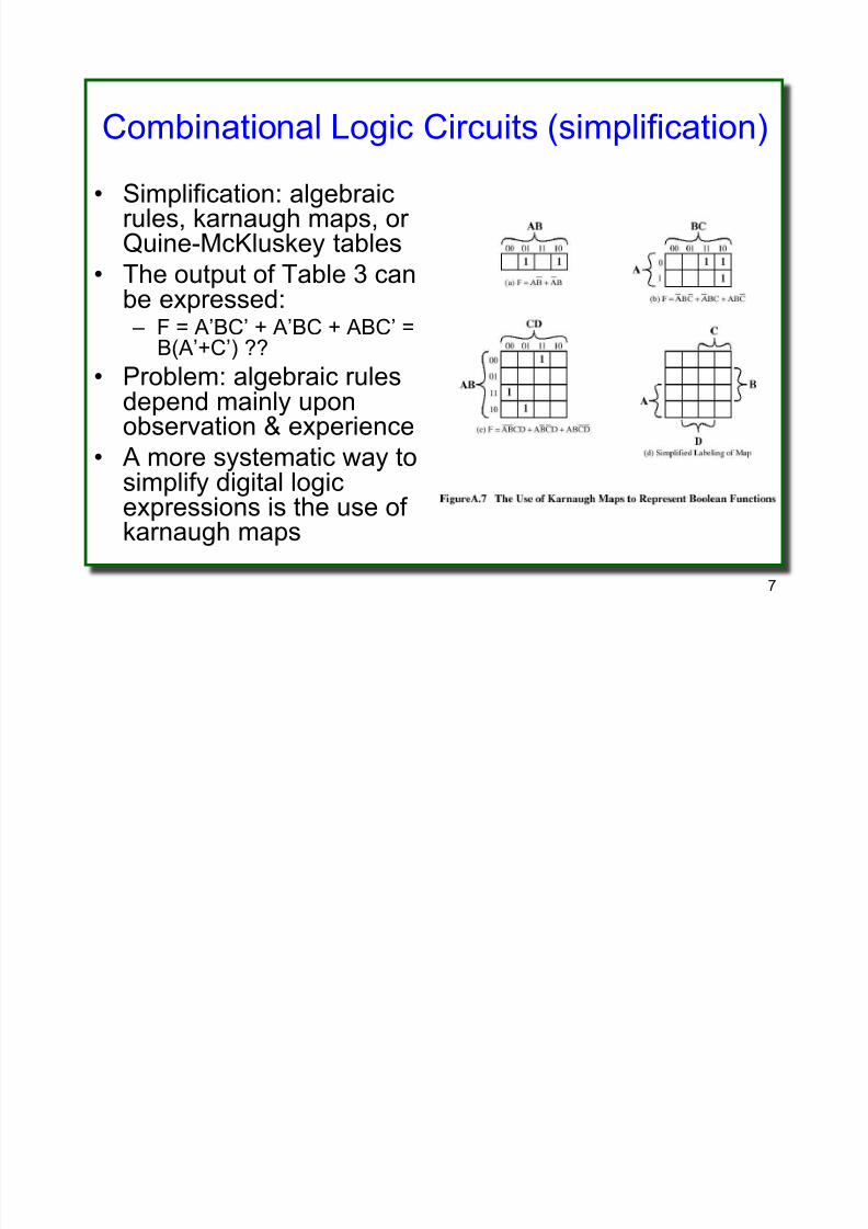
Combinational Logic Circuits (simplification)
• Simplification: algebraicrules, karnaugh maps, or Quine-McKluskey tables
• The output of Table 3 can
be expressed: – F = A’BC’ + A’BC + ABC’ =
B(A’+C’) ??
• Problem: algebraic rulesdepend mainly uponobservation & experience
• A more systematic way tosimplify digital logicexpressions is the use of karnaugh maps
8/6/2019 Introduction Digital Logic
http://slidepdf.com/reader/full/introduction-digital-logic 8/22
8
• The map is an array of 2n
squares (n # of inputs)
• How do you fill the map from a truth table??
• To use an expression, it should be in canonical form
• General rules of using the map:
–
Combine ones into groups of (1, 2, 4, 8, …) squares – Form the largest group size
– Form the min number of groups
– Two group should not intersect unless this will enable a smallgroup to be larger in size
• Some input combinations shall not occur and in this
situation we call the outputs, “do not care” conditions• These “ds” can be used as either 1 or 0
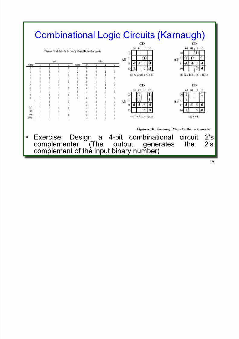
• Example: designing an incrementer for a BCD number,see Table 4 and Figure 10 in the following slide
Combinational Logic Circuits (Karnaugh)
8/6/2019 Introduction Digital Logic
http://slidepdf.com/reader/full/introduction-digital-logic 9/22
9
Combinational Logic Circuits (Karnaugh)
• Exercise: Design a 4-bit combinational circuit 2’scomplementer (The output generates the 2’scomplement of the input binary number)
8/6/2019 Introduction Digital Logic
http://slidepdf.com/reader/full/introduction-digital-logic 10/22
10
• Quine-Mckluskey Algorithm is a systematic method toobtain the minimum form of a Boolean expression
• The details of the algorithm are described in thehandout
• The algorithm is best described by an example
• Minimize the following function
• F(A, B, C, D) = Σ (1, 5, 6, 7, 11, 12, 13, 15)• This can be expresses as F = A’B’C’D + A’BC’D +
A’BCD’ + A’BCD + AB’CD + ABC’D’ + ABC’D + ABCD
• The minimal expression is F = A’C’D + A’BC + ABC’ +
ACD• Quiz: Try it using the decimal approach
Combinational Logic Circuits (QMA)
8/6/2019 Introduction Digital Logic
http://slidepdf.com/reader/full/introduction-digital-logic 11/22
11
• NAND and NOR implementation
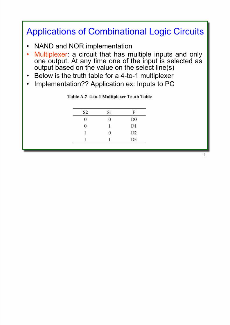
• Multiplexer : a circuit that has multiple inputs and onlyone output. At any time one of the input is selected asoutput based on the value on the select line(s)
• Below is the truth table for a 4-to-1 multiplexer
• Implementation?? Application ex: Inputs to PC
Applications of Combinational Logic Circuits
8/6/2019 Introduction Digital Logic
http://slidepdf.com/reader/full/introduction-digital-logic 12/22
12
• A decoder has n input lines and 2n output lines. Onlyone output line is selected based on the input
• Example: Instruction Op code decoding
• With an additional input line, a decoder can be used asa demultiplexer which connects its single input to one of
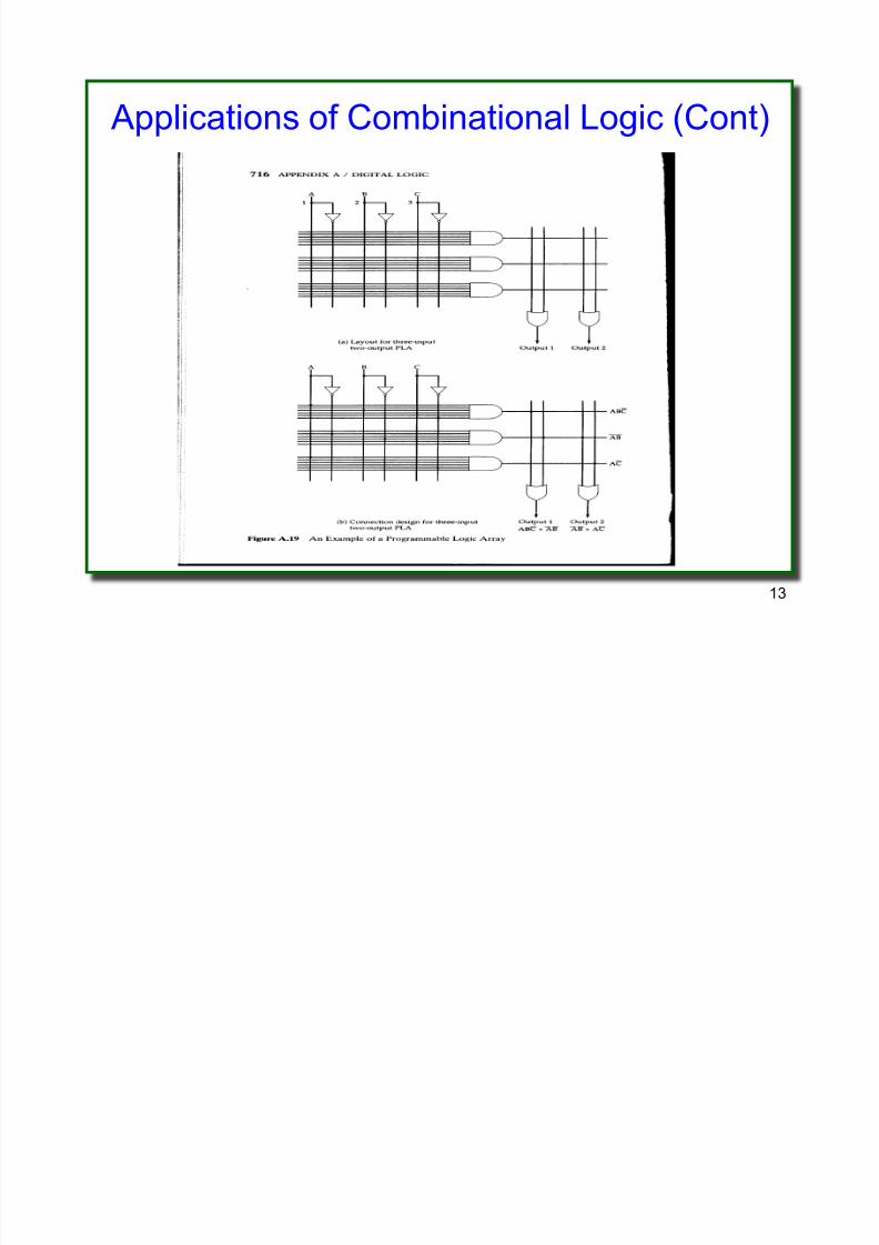
its outputs based on the value on the address lines• PLA (Programmable Logic Array) has the objective of
developing a general purpose chip that can be readilyadapted to specific purposes
• It can be implemented by making every possibleconnection through a fuse. Undesired connections areremoved by blowing their fuses
• This kind is called field-PLA• See next slide
Applications of Combinational Logic (Cont)
8/6/2019 Introduction Digital Logic
http://slidepdf.com/reader/full/introduction-digital-logic 13/22
13
Applications of Combinational Logic (Cont)
8/6/2019 Introduction Digital Logic
http://slidepdf.com/reader/full/introduction-digital-logic 14/22
14
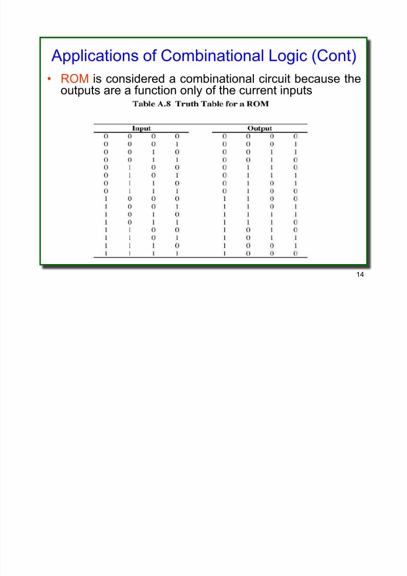
• ROM is considered a combinational circuit because theoutputs are a function only of the current inputs
Applications of Combinational Logic (Cont)
8/6/2019 Introduction Digital Logic
http://slidepdf.com/reader/full/introduction-digital-logic 15/22
15
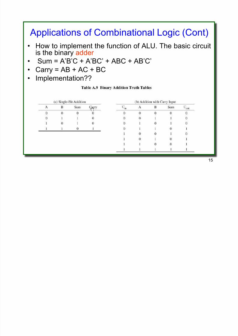
• How to implement the function of ALU. The basic circuitis the binary adder
• Sum = A’B’C + A’BC’ + ABC + AB’C’
• Carry = AB + AC + BC
• Implementation??
Applications of Combinational Logic (Cont)
8/6/2019 Introduction Digital Logic
http://slidepdf.com/reader/full/introduction-digital-logic 16/22
16
• We can form n-bit adders by cascading n 1-bit adders
• The carry of a unit is fed to the next one (ripple adders)
• The problem with ripple adders is the increasing delay
• The solution is using carry lookahead technique
•
C0 = A0B0• C1 = A1B1 + A1A0B0 + B1A0
• C2, ….. etc.
• Usually a full adder (32-bit say) is constructed from anumber of modules (8-bit) adders where the carries arerippled between modules but each module uses carry
lookahead to derive internal carry signals.• Quiz: Design an 8-bit carry lookahead adder using two
4-bit units (derive all internal and external carry signalsand draw the final diagram)
Applications of Combinational Logic (Cont)
8/6/2019 Introduction Digital Logic
http://slidepdf.com/reader/full/introduction-digital-logic 17/22
17
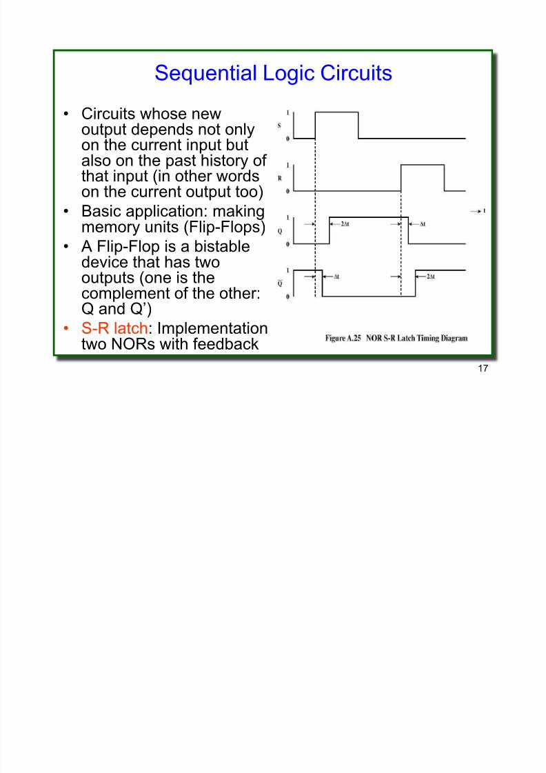
Sequential Logic Circuits
• Circuits whose newoutput depends not onlyon the current input butalso on the past history of that input (in other words
on the current output too)• Basic application: making
memory units (Flip-Flops)
• A Flip-Flop is a bistabledevice that has twooutputs (one is thecomplement of the other:Q and Q’)
• S-R latch: Implementationtwo NORs with feedback
8/6/2019 Introduction Digital Logic
http://slidepdf.com/reader/full/introduction-digital-logic 18/22
18
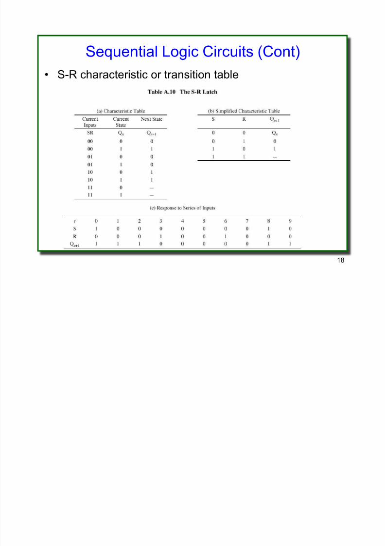
Sequential Logic Circuits (Cont)
• S-R characteristic or transition table
8/6/2019 Introduction Digital Logic
http://slidepdf.com/reader/full/introduction-digital-logic 19/22
19
Sequential Logic Circuits (Applications)
• Clocked S-R Flip-Flop: Using AND at the input
• D Flip-Flop: One input is negated and used as thesecond input. Implementation & characteristic table
• J-K Flip-Flop: it differs in that all input combinations are
allowed. The last case (J=K=1) causes the output totoggle, a very important feature
• Implementation and table
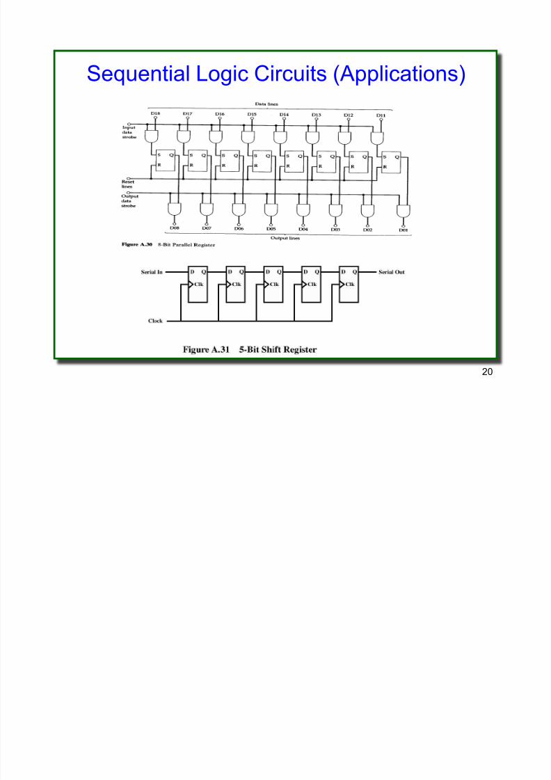
• Flip-Flips are used to implement registers. There are twotypes of registers
• A parallel register is a set of 1-bit memories that can be
read or written simultaneously. See the following slide• A shift register implements the shits function. See the
following slide
8/6/2019 Introduction Digital Logic
http://slidepdf.com/reader/full/introduction-digital-logic 20/22
20
Sequential Logic Circuits (Applications)
8/6/2019 Introduction Digital Logic
http://slidepdf.com/reader/full/introduction-digital-logic 21/22
21
Sequential Logic Circuits (Applications)
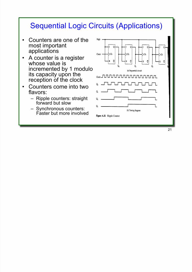
• Counters are one of themost importantapplications
• A counter is a register whose value isincremented by 1 moduloits capacity upon thereception of the clock
• Counters come into twoflavors: – Ripple counters: straight
forward but slow – Synchronous counters:
Faster but more involved
8/6/2019 Introduction Digital Logic
http://slidepdf.com/reader/full/introduction-digital-logic 22/22
22
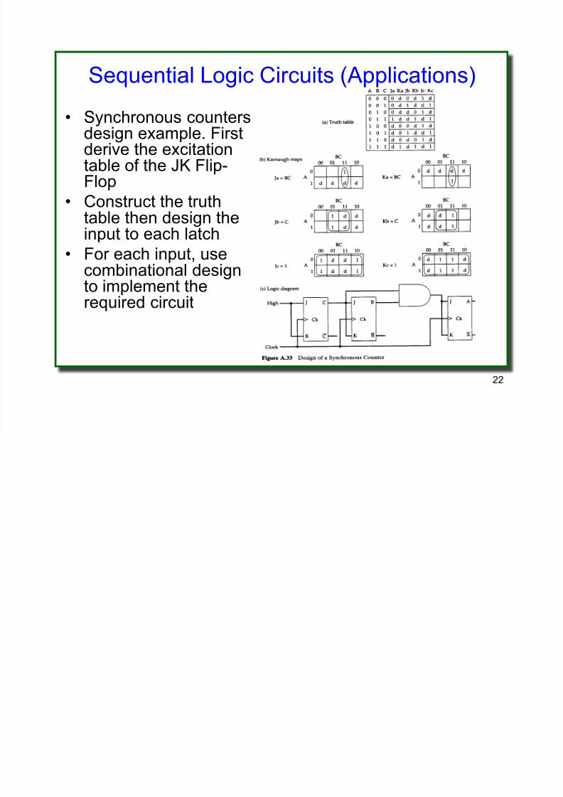
Sequential Logic Circuits (Applications)
• Synchronous countersdesign example. Firstderive the excitationtable of the JK Flip-Flop
• Construct the truthtable then design theinput to each latch
• For each input, usecombinational designto implement therequired circuit