Embed Size (px)
Citation preview

Dielectric resonator antenna for Short Range Wireless Communication Applications
A THESIS
SUBMITTED IN PARTIAL FULFILLMENT OF THE
REQUIREMENTS FOR THE DEGREE OF
MASTER OF TECHNOLOGY
IN
TELEMATICS AND SIGNAL PROCESSING
BY
MAHENDER P
Roll No. – 209EC1114
Department of Electronics and Communication
Engineering
National Institute of TechnologyRourkela-769008
2013

Dielectric resonator antenna for Short Range
Wireless Communication Applications
A THESIS
SUBMITTED IN PARTIAL FULFILLMENT OF THE
REQUIREMENTS FOR THE DEGREE OF
MASTER OF TECHNOLOGY
IN
TELEMATICS AND SIGNAL PROCESSING
BY
MAHENDER P
Roll No. – 209EC1114
Under the Supervision of
Prof. S K Behera
Mr. Vivek Angadala
Department of Electronics and Communication
Engineering
National Institute of TechnologyRourkela-769008
2013

Department of Electronics and Communication Engineering
National Institute of Technology Rourkela Date: 20-05-2013
CERTIFICATE
This is to certify that this thesis entitled “Dielectric resonator antenna for Short Range
Wireless Communication Applications” submitted by Mr. MAHENDER P , in partial fulfilment
of the requirements for the award of Master of Technology Degree in Electronics and
Communication Engineering with specialization in “Telematics and Signal Processing” during
session 2011-13 at the National Institute of Technology, Rourkela (Deemed University) is an
authentic work carried out by him under my supervision and guidance.
To the best of my knowledge, the matter embodied in the thesis has not been submitted to
any other University/Institute for the award of any degree or diploma.
Dr. S K Behera
.

ACKNOWLEDGEMENTS
This project is by far the most significant accomplishment in my life and it would be
impossible without people who supported me and believed in me.
I would like to extend my gratitude and my sincere thanks to my honorable, esteemed
supervisor Prof. S K Behera. He is not only a great lecturer with deep vision but also and
most importantly a kind person. I sincerely thank for his exemplary guidance and
encouragement. His trust and support inspired me in the most important moments of making
right decisions and I am glad to work with him. I would like to special thank for Prof. S
Meher Head of the Department of Electronics and Communication Engineering, NIT,
Rourkela, for providing us with best facilities in the Department and his timely suggestions.
I want to thank all my teachers Prof. S.K Patra, Prof. K. K. Mahapatra, Mr. Vivek
Angadala for providing a solid background for my studies and research thereafter. They have
been great sources of inspiration to me and I thank them from the bottom of my heart.
I would like to thank all my friends and especially my classmates and Mr. S.
Natarjamani and Mr. Yogesh Choukiker for all the thoughtful and mind stimulating
discussions we had, which prompted us to think beyond the obvious. I’ve enjoyed their
companionship so much during my stay at NIT, Rourkela.
I would like to thank all those who made my stay in Rourkela an unforgettable and
rewarding experience.
Last but not least I would like to thank my parents, who taught me the value of hard
work by their own example. They rendered me enormous support during the whole tenure of
my stay in NIT Rourkela.
Mahender P

i
ABSTRACT
Present scenario of communication, all wired ones replacing with wireless. So, to
achieve efficient communication in wireless technology, efficient radiators required. One
such efficient radiators is Dielectric resonator antenna. The extremely wide spectrum of 3.1
to 10.6 GHz with 15 bands of bandwidth greater than 500 MHz and power limit less than -
41.3 dBm/MHz announced by FCC for Ultra wide band. The release of this Spectrum has
rapidly increased the research in UWB technology for communications, radar imaging, and
localization applications. Radio systems based on UWB technology offer opportunities for
transmission of high data rate signals, coding for security and low probability of intercept,
especially in multi user network applications . UWB communication systems have the
promise of very high bandwidth, reduced fading from multipath in mobile communication
and low power requirements. In general, UWB radio systems transmit and receive temporally
short pulses without carriers or modulated short pulses with carriers. Carrier free UWB radio
systems usually employ very short pulses in the order of sub nanosecond (ns) as opposed
traditional communication schemes which send sinusoidal waves. DRA is one of the best
antennas for UWB applications due to its attractive features like high radiation efficiency,
low dissipation loss, small size, light weight, and low profile. Moreover, DRAs which
possess a high degree of design flexibility, have emerged as an ideal candidate for wide band,
high efficiency, and cost-effective applications. Second antenna is designed which resonates
at 5.5 GHz which is suitable for 802.11a WLAN applications. The return loss of proposed
antenna is -22.7dB at 5.5GHz. Third antenna is designed to resonate at two different
frequencies one at 2.42 GHz and other at 9.13 GHz with dielectric constant of 10. The
feeding mechanism used is CPW feeding. This CPW feeding structure has many useful
characteristics like low radiation leakage, less dispersion, little dependency of the
characteristics impedance on substrate height and unipolar configuration. Same antenna is
fabricated with dielectric constant of 2.1 and measured the return loss, which is resonating at
3.5 GHz which can be used in WIMAX. The simulated and measured results shows that as
the dielectric constant of DRA is increasing the resonant frequency shifts towards the lower
frequency and as the dielectric constant is decreasing the resonant frequency is shifting
towards higher frequency and the frequency of operation is also changing.

CONTENTS
Abstract i
List of figure and Table ii
Chapter 1 Thesis overview 1
1.1 Introduction 2
1.2 Literature Review 4
1.3 Scope of this project 5
1.4 Thesis Outline 5
Chapter 2 Dielectric Resonator Antenna 7
2.1 Dielectric Resonator Antenna Theory 8
2.2 Basic Characteristics 8
2.3 Advantages 10
2.4 Feeding Methods 13
2.4.1 Coaxial feed 13
2.4.2 Slot aperture 14
2.4.3 Microstrip line feed 15
2.4.4 Co-planar waveguide feed 17
2.4.5 Dielectric image guide 18
2.5 Analytical Evaluation of a DRA 19
2.5.1 Green’s function analysis 19
2.5.2 Numerical methods for analyzing DRAs 20
2.5.3 Frequency domain analysis 20
2.5.4 Time domain analysis 21
Chapter 3 Antenna Parameter 22
3.1 Gain and directivity 23
3.2 Antenna Polarization 24
3.3 Input impedance 24
3.4 Voltage standing wave ratio 25
3.5 Bandwidth 25
3.6 Quality factor. 26
Chapter 4 H-Shaped UWB Dielectric Resonator Antenna 28
4.1 Introduction 29
4.2 Geometry of proposed Antenna 30
4.3 Simulation Setup and Result 31
4.3.1 Simulation setup 31
4.3.2 Return loss and antenna bandwidth 32
4.3.3 Input impedance 33
4.3.4 Gain Vs. Frequency plot 33
4.3.5 Performance parameters of antenna 34
4.3.6 Time Domain Characteristics 36
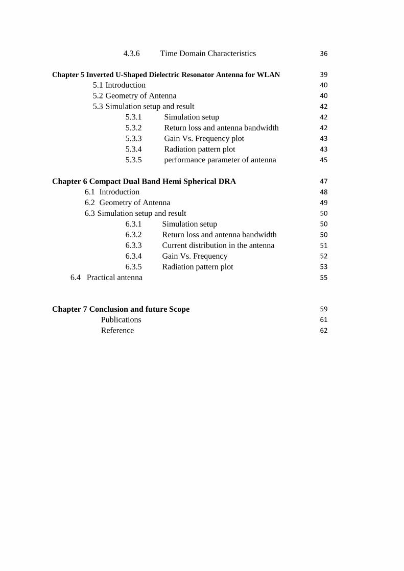
Chapter 5 Inverted U-Shaped Dielectric Resonator Antenna for WLAN 39
5.1 Introduction 40
5.2 Geometry of Antenna 40
5.3 Simulation setup and result 42
5.3.1 Simulation setup 42
5.3.2 Return loss and antenna bandwidth 42
5.3.3 Gain Vs. Frequency plot 43
5.3.4 Radiation pattern plot 43
5.3.5 performance parameter of antenna 45
Chapter 6 Compact Dual Band Hemi Spherical DRA 47
6.1 Introduction 48
6.2 Geometry of Antenna 49
6.3 Simulation setup and result 50
6.3.1 Simulation setup 50
6.3.2 Return loss and antenna bandwidth 50
6.3.3 Current distribution in the antenna 51
6.3.4 Gain Vs. Frequency 52
6.3.5 Radiation pattern plot 53
6.4 Practical antenna 55
Chapter 7 Conclusion and future Scope 59
Publications 61
Reference 62

ii
FIGURES AND TABLES
Fig. 2.1 DRAs of various shapes (cylindrical, rectangular, hemispherical, low-
profile circular-disk, low-profile triangular) 10
Fig. 2.2 Probe-fed Dielectric resonator antennas 14
Fig. 2.3 Slot-fed Dielectric resonator antennas 15
Fig. 2.4 Microstrip-fed DRA 16
Fig. 2.5 Co-planar loop-fed DRA 17
Fig. 2.6 Dielectric image guide-fed DRA 18
Fig. 4.1 Geometry of H-Shaped UWB DRA 30
Fig. 4.2 Geometry of H-Shaped DRA 31
Fig. 4.3 Geometry of Ground plane 31
Fig. 4.4. Return Loss for various feed lengths. 32
Fig. 4.5 Variation of Return Loss with and without ground slot 32
Fig. 4.6. Input impedance of the proposed antenna. 33
Fig. 4.7 Gain of the proposed antenna 34
Fig. 4.8 Path loss of antenna (a) Face to Face (b) Side by Side 35
Fig. 4.8.I Group delay of proposed antenna 36
Fig. 4.9 Input , Transmitted and Received signals 36
Fig. 4.10. Received signals when antennas Face to Face and Side by Side 37
Fig. 5.1. Geometry of proposed DR antenna. (a) Top-view (b) Side-view 41
Fig. 5.2. Return Loss for various h values. 42
Fig.5.3. Simulated Gain of the proposed Antenna. 43
Fig. 5.4. Radiation patterns of proposed antenna 45
Fig. 5.5. Dispersion property of proposed antenna (Path loss) 46
Fig. 6.1. Proposed antenna (a) Front view (b) Feed geometry 50
Fig. 6.2. Simulated Return loss of the proposed antenna 51
Fig. 6.3. Current distribution at (a) 2.4GHz (b) 9GHz 52
iii
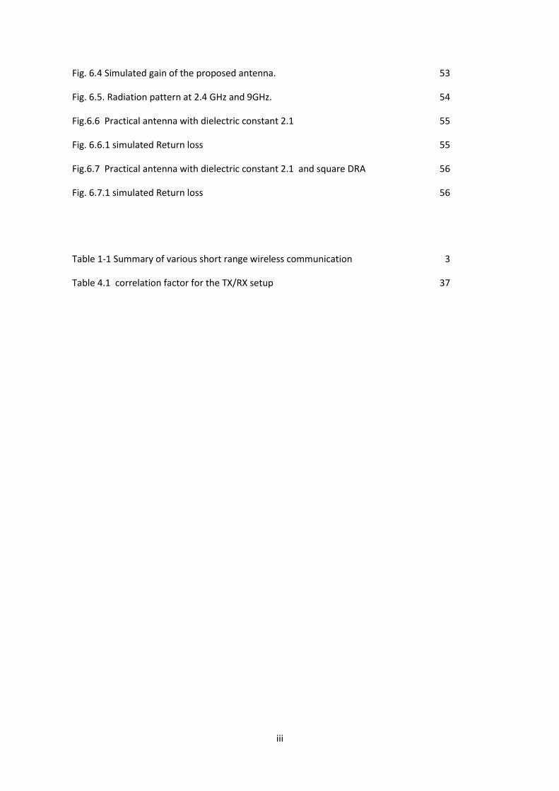
Fig. 6.4 Simulated gain of the proposed antenna. 53
Fig. 6.5. Radiation pattern at 2.4 GHz and 9GHz. 54
Fig.6.6 Practical antenna with dielectric constant 2.1 55
Fig. 6.6.1 simulated Return loss 55
Fig.6.7 Practical antenna with dielectric constant 2.1 and square DRA 56
Fig. 6.7.1 simulated Return loss 56
Table 1-1 Summary of various short range wireless communication 3
Table 4.1 correlation factor for the TX/RX setup 37


1
CHAPTER
1
THESIS OVERVIEW

2
1.1 Introduction
Short range wireless communication such as WLAN and Ultra-Wideband (UWB) are
becoming more popular within the market place and as a research area. They both enable users to
exchange data and to connect telecommunications devices over a short range without the use of a
“hard wired” connection. Antennas are an essential part of WLAN and Ultra-Wideband (UWB)
devices with conflicting demands of small size and high antenna efficiency. Thus, the
implementation of the exclusive small antennas with acceptable gain is highly desirable. In this
thesis, three different compact antennas are proposed for use in UWB and WLAN.
With the use of wireless technology, the construction of a communication system is
more convenient and cost effective, as there is no cable installation between the user devices and
transmitters. Now days, wireless technology is inexpensive and mature enough to apply in short
range communications, which are commonly used in portable devices, like remote control,
wireless microphone, DECT cordless phone and wireless USB devices, etc. On the other hand,
the environmental issue has become a hot topic that has made an impact into many areas, such as
green electronic, green agriculture, green chemical industry and green wireless etc. Short-range
wireless communication is classified as green wireless in as much as it exhibits characteristics
like low power consumption, low RF radiation power, and low cost.
In recent years, some newer and more advanced wireless technologies have been
developed or are under development, and include Bluetooth, ZigBee, Wi-Fi (802.11a, b, g) and
Ultra-Wideband (UWB). These technologies deliver wire-like performance in an indoor wireless
environment. A summary of the different characteristics for short-range wireless communication
is shown in Table 1-1.

3
Standard 802.11 802.11a 802.11b 802.11g
Frequency(GHz) 2.45 5 2.4 2.4
Speed(Mbps) 0.72 54 11 54
Range 10m 50m 100m 100m
Applications Bluetooth WiFi(a) WiFi(b) WiFi(g)
Table 1-1 Summary of various short range wireless communications
Antennas are very important for these wireless technologies. Their antenna design has
become a very hot research topic as antennas form the essential part of every wireless device.
Without antennas, wireless signals cannot be radiated efficiently into free space thus making
the device inoperable. The antenna size is directly related to the size of the devices. With the
advent of system on chip, the size of the devices can be dominated by the size of the
antenna, thus a device can now be made significantly smaller if the size of the antenna
can be made small. In this thesis, three different antennas for UWB and WLAN are proposed.

4
1.2 Literature Review
For many years, the dielectric resonator has primarily been used in microwave circuits,
such as oscillators and filters. If the shielding is removed and with the proper excitation to
launch the appropriate mode, these same dielectric resonators can actually become efficient
radiators. Furthermore, by lowering their dielectric constant, the radiation can be
maintained over a relatively broad band of frequencies. Although open DRs were found to
radiate many years ago , the idea of using the DR as an antenna had not been widely
accepted until the original paper on the cylindrical dielectric resonator antenna (DRA) was
published in 1983 by S.A. Long , M.W. McAllister and L.C.Shen.
In the early 1990s, emphasis was placed on realizing various feeding mechanisms to excite
the DRAs and on applying various analytical or numerical techniques for determining the
input impedance and Q-factor. Focus was mainly on individual elements. A significant
amount of this characterization was carried out by two research teams: one was led by
Kishk, Glisson , and Junker and the other by Luk and Leung. By the mid-1990s more
attention was being given to linear and planar DRA arrays, ranging from simple two-
element arrays, up to complex phased arrays .This period also saw the development of
ferrite resonator antennas, DRAs operating at 40GHz, and DRAs with nearly 40%
impedance bandwidth. Many of the recent advances were profiled by petosa et al.
Since the late 1990s more researchers have entered the field , and the yearly number of
publications has grown. Emphasis has been on a compact designs to address the needs of
portable wireless applications and on new DRA shapes or hybrid antennas for enhanced
5
bandwidth performance to meet the requirements for emerging broadband or ultra-
wideband systems.
1.3 SCOPE OF THIS PROJECT
The scope of this work is to design a DRA which can be used for UWB applications
according to the Federal communication commission specifications. That is used the
operating frequency band ranging from 3.1 to 10.6 GHz with the smaller possible distortion
of the UWB pulse. On the other hand Inverted U-Shaped Dielectric Resonator Antenna for
WLAN which operated at 5.5GHz and another Compact Dual Band Hemi Spherical
Dielectric Resonator Antenna which resonates at two different frequencies one at 2.4 GHz
and other at 9.10 GHz, are designed which can be used for wireless communication
applications.
1.4 THESIS OUTLINE
The outline of this thesis is as follows
Chapter 2:It presents the basic characteristics of Dielectric Resonator antenna, the
advantages and disadvantages of DRA, Feeding methods of DRA, Analytical Evaluation of
DRA like frequency domain analysis and time domain analysis are present in this chapter.
Chapter 3: In this chapter the basics of antenna parameters such as Gain and directivity,
polarization, input impedance, VSWR, bandwidth, Quality factor.

6
Chapter 4: This chapter describes H-Shaped UWB dielectric resonator Which covers the
entire UWB band, the shape of DRA is H-Shape. The other parameters like Return loss,
input impedance, gain performance parameters like path loss, group delay and time domain
characteristics are described in this chapter.
Chapter 5:This chapter describes Inverted U shaped dielectric resonator antenna for wlan
application. The other parameters like Return loss, gain, performance parameter i.e., path
loss and radiation pattern are described in this chapter.
Chapter 6:This chapter describes compact dual band hemispherical dielectric resonator
antenna. This antenna resonates at dual frequency one of this can be used for WLAN
applications. The other parameters like Return loss, gain, current distribution, and radiation
pattern are described in this chapter.
Chapter 7: This chapter describes the conclusion and future work.

7
CHAPTER
2
DIELECTRIC
RESONATOR
ANTENNA

8
2.1 Dielectric Resonator Antenna Theory
The dielectric resonator has primarily been used in microwave circuits, such as oscillators
and filters. If the shielding is removed and with the proper excitation to launch the appropriate
mode, these same dielectric resonators can actually become efficient radiators. Furthermore, by
lowering their dielectric constant, the radiation can be maintained over a relatively broad band of
frequencies. Various feeding mechanisms to excite the DRAs such as coaxial feed, slot aperture
feed, Microstrip line feed, Coplanar wave guide feed. These DRAs can be easily coupled to
integrated circuits. Since recent emphasis has been on a compact designs to address the needs of
portable wireless applications and on new DRA shapes or hybrid antennas for enhanced
bandwidth performance to meet the requirements for emerging broadband or ultra wideband
systems.
2.2 Basic characteristics
Dielectric resonator antennas (DRA) possess some peculiar properties which render them
very promising, especially for millimeter wave applications. Their high-radiation efficiency,
bandwidth and polarization flexibility make them by far superior to conventional microstrip
patch antennas (MPA). DRA are intrinsically immune to those surface wave power leakage and
conductor loss problems, which plagues the MPA and reduces their efficiency. DRA consists of
high dielectric constant materials, high quality factors and mounted on a grounded dielectric
substrate of lower permittivity. DRA is fabricated from low-loss and high relative dielectric
constant material of various shapes whose resonant frequencies are functions of the size, shape
and permittivity of the material. DRA can be in a few geometries including cylindrical,
rectangular, spherical, half-split cylindrical, disk, and hemispherical shaped. The DRAs have
properties such as low phase noise, compact size, frequency stability with temperature, ease of

9
integration with other hybrid MIC circuitries, simple construction and the ability to withstand
harsh environments. The DRA has some interesting characteristics, like the small size, ease of
fabrication; high radiation efficiency, increased bandwidth and low production cost. DRAs are
very promising for applications in wireless communications.
DRAs offer several attractive features including:
A wide range of dielectric constants can be used ( = 10 – 100), that allowing the
designer to have control over the physical size of the DRA and its bandwidth.
The Size of DRA is proportional to λ0/√ , where λ0 is the free space
wavelength at the resonant frequency, and is the dielectric constant of the
material.
DRAs can be designed to operate over a wide range of frequencies from 1.3 GHz
to 40 GHz.
High radiation efficiency (95%) due to the absence of conductor or surface wave
losses.
Several feeding mechanisms can be used (including slots, probes, microstrip lines,
dielectric image guide, and coplanar waveguide lines) to efficiently excite DRAs.
DRA can be excited by several modes, many of which radiate pattern similar to
short electric or magnetic dipoles, producing either broadside or Omni directional
radiation patterns for different coverage requirements.
By selecting a dielectric material with low-loss characteristics, high-radiation
efficiency can be maintained, even at millimeter-wave frequencies, due to an
absence of surface waves and minimal conductor losses associated with the DRA.
A Wide control over size and bandwidth

10
A tight tolerance: ± 1- 5%,
A high quality factor Q: up to 10000 (f = 10GHz)
A Wide range of temperature coefficient of resonance frequency: (-12…+30)
ppm/oC
A Tolerance ± 0.5; ±1.0; ±2.0 ppm/ oC.
Fig. 2.1 DRAs of various shapes (cylindrical, rectangular, hemispherical, low-profile circular-disk,
low-profile triangular)
2.3 ADVANTAGES
In the past few years, extensive studies on the DRA have been focused on resonators of
various shapes, the feeding techniques, and bandwidth enhancement methods. Specific features
of DRAs have made them suitable for a variety of applications specially millimeter wave
(MMW) applications. DRAs can be easily coupled to almost all types of transmission lines. They
can be integrated easily with MMIC circuits. In MMW applications conductor loss of metallic
antennas become severe and the antenna efficiency decreases significantly, conversely the only
loss for a DRA is that due to the imperfect material of the DRA which can be very small in
practice. Therefore DRAs have high radiation efficiency. In comparison to microstrip antennas,

11
DRAs have wider impedance bandwidths. For a typical DRA with dielectric constant of 10 the
impedance bandwidth of 10% can be achieved. Avoidance of surface waves is another attractive
advantage of DRAs over microstrip antennas. Single DRAs of different shapes has been
possible, including rectangular, cylindrical, hemispherical, triangular, conical, etc. Among these
different shapes cylindrical and rectangular are the most common and the rectangular has the
advantage of having one more degree of freedom for design purposes. There are a variety of feed
configurations, which electromagnetic fields can be coupled to DRAs. Most common feed
arrangements are microstrip aperture coupling, direct microstrip coupling, probe coupling and
conformal strip coupling. Among these feed configurations, aperture coupling is more suitable
for MMW applications. In aperture coupling configuration, since the DRA is placed on the
ground plane of the microstripfeed, Figure 2.1 DRAs of various shapes (cylindrical, rectangular,
hemispherical, low-profile circular-disk, low-profile triangular) parasitic radiation from the
microstrip line is avoided. Isolation of the feed network from the radiating element is another
advantage of the aperture coupling method.
Dielectric resonator antennas (DRAs) have been extensively used for numerous
applications since they have many attractive characteristics such as low profile, light weight, low
cost, and inherently wide bandwidth. They could be used for numerous applications as both
individual elements and in an array environment. In addition, wide bandwidth, low cost, low
dissipation loss at high frequency, and high radiation efficiency are the inherent advantages of
DRAs over conventional patch antennas. Compared with Microstrip antennas, which suffer from
higher conduction loss and surface waves in antenna array applications, DRAs have high
radiation efficiency and high power handling capability due to lack of metallic loss. Unlike the
microstrip antenna, DRA does not support surface waves if placed on a ground plane directly. In

12
recent years, DRAs have been considered as potential antennas for mobile phone applications. A
general problem in the miniaturization of RF resonators used in filters and small antennas is
decrease of efficiency, due to conductor losses. In DRAs, lower conductor losses, compared to
those in typical metal antennas such as microstrip patches can be expected because DRAs have
fewer metal parts. Thus, DRAs are good potential alternatives, especially when very small
antenna elements are needed. In addition, they can be easily incorporated into microwave
integrated circuits because they can be fabricated directly on the printed circuit board (PCB) of
the phone. Specific features of DRAs have made them suitable for a variety of applications
specially MMW applications. DRAs have small size and low cost. They can be easily coupled to
almost all types of transmission lines.
Dielectric resonator antennas have several advantages compared to conventional
microwave antennas, and therefore many applications cover the broad frequency range. Some of
the principal advantages of dielectric resonator antennas compared to conventional microstrip
antennas are:
DRA has a much wide impendence bandwidth than microstrip antenna because it
radiates through the whole antenna surface except ground port while microstrip
antenna radiate only through two narrow radiation slots.
Higher efficiency.
Avoidance of surface waves is another attractive advantage of DRAs over
microstrip antennas
However, dielectric resonator antennas have some advantages:
Light weight, low volume, and low profile configuration, which can be made
conformal;

13
DRA has high degree of flexibility and versatility, allowing for designs to suit a
wide range of physical or electrical requirements of varied communication
applications.
High radiation efficiency
High dielectric strength and higher power handling capacity
In DRA, various shapes of resonators can be used (rectangular, cylindrical,
hemispherical, etc.) that allow flexibility in design.
Several feeding mechanisms can be used (probes, slots, microstrip lines, dielectric
image guides, and coplanar waveguide lines) to efficiently excite DRAs, making
them amenable to integration with various existing technologies.
2.4Feeding Methods
There are several techniques available to feed or transmit electromagnetic energy to a
dielectric resonator antenna. The five most popular feeding methods are the coaxial probe, slot
aperture, microstrip line, co-planar coupling and dielectric image guide.
2.4.1 Coaxial Feed
The Coaxial feed or probe feed is a very common technique used for feeding dielectric
resonator antennas as shown in figure 2.2. In this method, the probe can either be placed adjacent
to the DRA or can be embedded within it. The amount of coupling can be enhanced by adjusting
the probe height and the DRA location. In DRA, various modes can be excited depending on the
location of the probe. For the probe located adjacent to the DRA, the magnetic fields of the
TE11δ mode of the rectangular DRA are excited and radiate like a horizontal magnetic dipole.
For a probe located in the center of a cylindrical DRA, the TE011 mode is excited and radiating

14
like a vertical dipole. Another benefit of using probe coupling is that one can couple directly into
a 50Ω system, without the requirement for a matching network. Probes are suitable at lower
frequencies where aperture coupling may not be applied due to the large size of the slot required.
Fig. 2.2 Probe-fed Dielectric resonator antennas
2.4.2 Slot Aperture
In slot aperture method, a DRA is exciting through an aperture in the ground plane upon
which it is placed. Aperture coupling is applicable to DRAs of any shapes such as rectangular,
cylindrical or hemispherical. The aperture works like a magnetic current running parallel to the
size of the slot, which excites the magnetic fields in the DRA. The aperture consists of a slot cut
in a ground plane and fed by a microstrip line below the ground plane. For avoiding spurious
radiation, feed network is located below the ground plane. Moreover, slot coupling is an
attractive technique for integrating DRAs with printed feed structures. The coupling level can be
changed by moving the DRA with respect to the slot. Generally, a high dielectric material is used
for the substrate and a thick, low dielectric constant material is used for the top dielectric

15
resonator patch to optimize radiation from the antenna. The main drawback of this feed
technique is that it is problematic to fabricate due to multiple layers, which also increases the
antenna thickness. This feeding method also provides narrow bandwidth (up to 21%) .
Fig. 2.3 Slot-fed Dielectric resonator antennas
2.4.3 Microstrip Line Feed
In this type of feed technique, a conducting strip is connected directly to the edge of the
patch as shown in figure 2.4. A common method for coupling to dielectric resonators in
microwave circuits is by proximity coupling to microstrip lines. Microstrip coupling will excite
the magnetic fields in the DRA to create the short horizontal magnetic dipole mode. The level of
coupling can be changed by the lateral location of the DRA with respect to the microstrip line
and on the relative permittivity of the DRA .
In DRAs, the amount of coupling is generally quite small for requiring wide bandwidth.
Microstrip lines can be used as a series feed for a linear array of DRAs. This is an easy feeding

16
technique, since it offers ease of fabrication and simplicity in modeling along with impedance
matching. However as the thickness of the dielectric substrate being used, rises, surface waves
and spurious feed radiation also rises, which hampers the bandwidth of the antenna. One
drawback of this method is that the polarization of the array is analyzed by the orientation of the
microstrip line such as the direction of the magnetic fields in the DRA will be parallel to the
microstrip line.
Fig. 2.4 Microstrip-fed DRA
In DRAs, the amount of coupling is generally quite small for requiring wide bandwidth.
Microstrip lines can be used as a series feed for a linear array of DRAs. This is an easy feeding
technique, since it offers ease of fabrication and simplicity in modeling along with impedance
matching. However as the thickness of the dielectric substrate being used, rises, surface waves
and spurious feed radiation also rises, which hampers the bandwidth of the antenna. One
drawback of this method is that the polarization of the array is analyzed by the orientation of the

17
microstrip line such as the direction of the magnetic fields in the DRA will be parallel to the
microstripline .
2.4.4 Co-Planar waveguide Feed
The Co- planar feed is a very common technique used for coupling in dielectric resonator
antennas. Here, figure 2.5 shows a cylindrical DRA coupled to a co-planar loop. The coupling
level can be adjusted by locating the DRA over the loop.
Fig. 2.5 Co-planar loop-fed DRA
The coupling behavior of the co-planar loop is similar to coaxial probe, but the loop offers the
advantage of being non-obtrusive. By moving the loop from the edge of the DRA to the center,
one can couple into either the HE11δ mode or the TE011 mode of the cylindrical DRA.

18
2.4.5 Dielectric Image Guide
Dielectric image guide is another attractive coupling technique in DRAs, as shown in
figure 2.6. Dielectric image guides offer advantages over microstrip at millimeter–wave
frequencies since they do not suffer as severely from conductor losses. As with microstriplines,
the amount of coupling to the DRA is generally quite small, especially for DRAs with Slower
permittivity values, although it may be possible to increase the coupling by operating the guide
closer to the cut-off frequency. The dielectric image guide is thus best utilized as a series feed to
a linear array of DRAs.
Fig. 2.6 Dielectric image guide-fed DRA

19
2.5 Analytical Evaluation of Dielectric Resonator Antenna
In designing, input impedance is the important parameter which is a feed to excite the
DRA. Input impedance as a function of frequency is to determine the bandwidth of operation and
for matching the antenna to the circuit. Unfortunately, there are no simple closed-form
expressions for predicting the input impedance of the DRA when excited by a particular feed and
rigorous analytical. Here, some of the techniques that have been used to predict the input
impedance for DRAs excited by the various feed.
2.5.1 Green’s function analysis
For a probe-fed DRA, the input impedance (Zin) can be determined using the following equation:
∫ (2.1)
E= Electric fields of the DRA
Js = Applied source current density on the probe
IO = Magnitude of the current on the probe
The electric fields of the DRA depend on the source excitation and determined by using:
∫ (2.2)
Here, G represents Green‘s function for the DRA. By using some simple assumptions about a
single-mode operation and the currents on the probe, the Green‘s function for a hemispherical
DRA was first derived and was then used to predict the input impedance of the probe-fed DRA
operating in the TE111 mode. This technique was also applied to a probe–fed hemispherical
DRA operating in the TM101 mode. The input impedance of conformal strip feeds and aperture
feeds can also be analyzed using Green‘s function. The advantage to this technique is the

20
relatively fast computation time required to obtain the input impedance. It is useful method for
analysing the effects of altering probe dimensions and probe location and can be used for
optimizing the input impedance. The main drawback is its limitation only to hemispherical DRA
geometries. For other DRA shapes, different analytical techniques are required.
2.5.2 Numerical methods for analyzing DRAs
Numerical methods for analyzing DRAs can be categorized into two groups, frequency
domain technique and time domain technique. Each category offers advantages for particular
antenna geometries.
2.5.3 Frequency domain analysis
Two common frequency domain techniques that have been used to analyze DRAs are the
method of moments (MOM) and the finite element method (FEM). The MOM was first
developed for wire or metal antennas of arbitrary shape, but can be extended to include dielectric
materials by introducing equivalent currents. The MOM involves discrediting the antenna into a
number of small segments and solving for a set of unknown coefficient representing the current
on one segment due to a known incident field. Analysis of DRAs is not limited to a
hemispherical shape, and the technique can be used to also analyses simple cylindrical and
rectangular DRA shapes. Determining the DRA input impedance using the MOM technique will
require more computer memory and time than applying Green‘s function. Thus, MOM technique
is not convenient tool for optimizing the DRA performance. MOM is used to investigate the
effect of the air gaps and calculate internal field pattern of various modes of cylindrical DRAs.

21
The FEM (Finite element method) can be used to analyses DRAs of arbitrary shape.
Similar to the MOM, it involves a discretization of the geometry but whereas in the MOM only
the DRA and the ground plane require segmentation , in the FEM the entire volume surrounding
the DRA must also be discretized, thereby increasing the computational size of the problem. The
advantage of the FEM is that it does not require the formulation of equivalent currents and can
thus be readily applied to arbitrary shapes. Another advantage of the FEM is its availability as
commercial software where graphical user interfaces are provided to simplify the geometrical
definition of the problem. FEM is used to determine the effects of a finite ground plane on the
radiation pattern of a DRA.
2.5.4 Time domain analysis
There are two time domain techniques that have been applied to analyzing DRAs are the
finite difference time domain (FDTD) method and the transmission line method (TLM). These
techniques require the entire volume around the DRA to be discretized and thus can be memory
and time intensive. In it, wideband pulse used to excite the DRA, and by transforming the
solution into the frequency domain, the input impedance can be determined over a wide
frequency range. For frequency domain techniques, the problem would have to be re simulated at
every frequency of interest and obtaining the impedance response over a broad frequency range
could be very time consuming. With the frequency domain methods, the time domain methods
are good tools for analyzing the performance of a given DRA geometry, but are less useful for
optimizing the performance of DRAs. FDTD is used to calculate circular polarization patterns of
cross-shaped DRAs and input impedance of slot-fed rectangular DRA. Transmission line method
used to calculate input impedance of microstrip-fed multi-segment DRAs.
22
CHAPTER
3
ANTENNA PARAMETER

23
3.1 Gain and directivity
The gain of an antenna is the radiation intensity in a given direction divided by the radiation
intensity that would be obtained if the antenna radiated all of the power delivered equally to all
directions. The definition of gain requires the concept of an isotropic radiator; that is, one that
radiates the same power in all directions. An isotropic antenna, however, is just a concept,
because all practical antennas must have some directional properties. Nevertheless, the isotropic
antenna is very important as a reference. It has a gain of unity (g = 1 or G = 0 dB) in all
directions, since all of the power delivered to it is radiated equally well in all directions.
Although the isotopes are a fundamental reference for antenna gain, another commonly
used reference is the dipole. In this case the gain of an ideal (lossless) half wavelength dipole is
used. Its gain is 1.64 (G = 2.15 dB) relative to an isotropic radiator.
The gain of an antenna is usually expressed in decibels (dB). When the gain is referenced
to the isotropic radiator, the units are expressed as dBi; but when referenced to the half-wave
dipole, the units are expressed as dBd. The relationship between these units is
(3.1)
Directivity is the same as gain, but with one difference. It does not include the effects of power
lost (inefficiency) in the antenna. If an antenna were lossless (100 % efficient), then the gain and
directivity (in a given direction) would be the same.

24
3.2 Antenna Polarization
The term polarization has several meanings. In a strict sense, it is the orientation of the electric
field vector E at some point in space. If the E-field vector retains its orientation at each point in
space, then the polarization is linear; if it rotates as the wave travels in space, then the
polarization is circular or elliptical. In most cases, the radiated-wave polarization is linear and
either vertical or horizontal. At sufficiently large distances from an antenna, beyond 10
wavelengths, the radiated, far-field wave is a plane wave.
3.3 Input impedance
There are three different kinds of impedance relevant to antennas. One is the terminal impedance
of the antenna, another is the characteristic impedance of a transmission line, and the third is
wave impedance. Terminal impedance is defined as the ratio of voltage to current at the
connections of the antenna (the point where the transmission line is connected). The complex
form of Ohm’s law defines impedance as the ratio of voltage across a device to the current
flowing through it.
The most efficient coupling of energy between an antenna and its transmission line occurs when
the characteristic impedance of the transmission line and the terminal impedance of the antenna
are the same and have no reactive component. When this is the case, the antenna is considered to
be matched to the line. Matching usually requires that the antenna be designed so that it has
terminal impedance of about 50 ohms or 75 ohms to match the common values of available
coaxial cable.
25
3.4 Voltage Standing Wave Ratio
The standing wave ratio (SWR), also known as the voltage standing wave ratio (VSWR), is not
strictly an antenna characteristic, but is used to describe the performance of an antenna when
attached to a transmission line. It is a measure of how well the antenna terminal impedance is
matched to the characteristic impedance of the transmission line. Specifically, the VSWR is the
ratio of the maximum to the minimum RF voltage along the transmission line. The maxima and
minima along the lines are caused by partial reinforcement and cancellation of a forward moving
RF signal on the transmission line and its reflection from the antenna terminals.
If the antenna terminal impedance exhibits no reactive (imaginary) part and the resistive
(real) part is equal to the characteristic impedance of the transmission line, then the antenna and
transmission line are said to be matched. It indicates that none of the RF signal sent to the
antenna will be reflected at its terminals. There is no standing wave on the transmission line and
the VSWR has a value of one. However, if the antenna and transmission line are not matched,
then some fraction of the RF signal sent to the antenna is reflected back along the transmission
line. This causes a standing wave, characterized by maxima and minima, to exist on the line. In
this case, the VSWR has a value greater than one. The VSWR is easily measured with a device
and VSWR of 1.5 is considered excellent, while values of 1.5 to 2.0 is considered good, and
values higher than 2.0 may be unacceptable.
3.5 Bandwidth
The bandwidth of an antenna is defined as the range of frequency within the performance of the
antenna. In other words, characteristics of antenna (gain, radiation pattern, terminal impedance)
have acceptable values within the bandwidth limits. For most antennas, gain and radiation
pattern do not change as rapidly with frequency as the terminal impedance does. Since the

26
transmission line characteristic impedance hardly changes with frequency, VSWR is a useful,
practical way to describe the effects of terminal impedance and to specify an antenna’s
bandwidth.
For broadband antennas, the bandwidth is usually expressed as the ratio of the upper to
lower frequencies of acceptable operation. However, for narrowband antennas, the bandwidth is
expressed as a percentage of the bandwidth.
3.6 Quality factor
The quality factor is a figure-of-merit that representative of the antenna losses. Typically there
are radiation, conduction, dielectric and surface wave losses.
: Total quality of factor
: Quality factor due to radiation losses
: Quality factor due to conduction losses
: Quality factor due to dielectric losses
:quality factor due to surface wave
The quality factor, bandwidth and efficiency are antenna figures-of-merit, which are interrelated,
and there is no complete freedom to independently optimize each one.
For very thin substrates h << of arbitrary shapes including rectangular, there approximate
formulas to represent the quality factors of the various losses.
These can be expressed as
√

27
⁄
Where tan δ is the loss tangent of the substrate material, σ is the conductivity of the conductors
associated with the patch and ground plane, is the total conductance per unit length of the
radiating aperture.

28
CHAPTER
4
H-Shaped UWB
Dielectric Resonator
Antenna

29
4.1 INTRODUCTION
The extremely wide spectrum of 3.1 to 10.6 GHz with 15 bands of bandwidth greater
than 500 MHz and power limit less than -41.3 dBm/MHz announced by FCC for Ultra wide
band. The release of this Spectrum has rapidly increased the research in UWB technology for
communications, radar imaging, and localization applications. Radio systems based on UWB
technology offer opportunities for transmission of high data rate signals, coding for security and
low probability of intercept, especially in multi user network applications . UWB communication
systems have the promise of very high bandwidth, reduced fading from multipath in mobile
communication and low power requirements. In general, UWB radio systems transmit and
receive temporally short pulses without carriers or modulated short pulses with carriers. Carrier
free UWB radio systems usually employ very short pulses in the order of sub nanosecond (ns) as
opposed traditional communication schemes which send sinusoidal waves. Antenna plays a
major role in UWB applications because these antennas have to transmit short duration pulses
without any pulse spread and as accurately as possible.DRA is one of the best antennas for UWB
applications due to its attractive features like high radiation efficiency, low dissipation loss,
small size, light weight, and low profile. Moreover, DRAs which possess a high degree of design
flexibility, have emerged as an ideal candidate for wide band, high efficiency, and cost-effective
applications. Recently more and more Ultra wideband antenna designs have been proposed
especially Stacking of two DRAs, DRAs separated by wall, Antenna mounted on a vertical
ground plane.

30
4.2 GEOMETRY OF ANTENNA
The size of DRA is 14mm length and 16.3 mm width and 6 mm thickness with dielectric onstant
10.2, and it is placed on 26 × 28 mm2 substrate with dielectric constant 1.06 and thickness of 0.7
mm. The ground plane is partially printed below the substrate. The size of ground plane is 26 ×
11.7 mm2 on one side and a printed probe extends from the Microstrip line of the same width
that ends with the 50Ω line after certain length. The other parameters are FL1 = 5 mm, FL2 =14.1
mm, FW1=1.9 mm, FW2 =1 mm. A slot of 10 mm × 3.5 mm is made in the ground in order to
cover lower frequencies in the ultra-wide band.
Fig. 4.1 Geometry of H-Shaped UWB DRA
26 mm
28
mm
FL2
FL1
FW1
FW2

31
Fig. 4.2 Geometry of H-Shaped DRA
Fig. 4.3 Geometry of Ground plane
4.3 SIMULATED SETUP AND RESULTS
4.3.1 Simulation Setup
The commercial 3D full wave electromagnetic (EM) simulation software CST
Microwave studio is used for simulation. It analyzes 3D and multilayer structures of general
shapes. It has been widely used in the design of MICs, RFICs, patch antennas, wire antennas,
and other RF/wireless antennas. It can be used to calculate Return loss plot, VSWR, current
distributions, radiation patterns etc.
14
16
.3
m
m
5
m
m
5 mm
26 mm
11.7
mm
mm
3.5
mm

32
4.3.2 Return loss and Antenna Bandwidth
As described in chapter three, the bandwidth can be calculated from the return loss (RL)
plot. The bandwidth of the antenna is said to be those range of frequencies over which the
return loss is less than -10dB, which is equivalent to 2:1 VSWR. It was observed from
many trials of simulations by changing the size of feed line it is observed it was
approximately covering the UWB Fig.4.4, later the applying slot on the ground plane
UWB is totally covered.Fig.4.5 Compares return loss with and without ground slot. With
ground slot total ultra wide band is covered. The slot in the ground plane is affecting the lower
frequencies.
4 6 8 10
-50
-40
-30
-20
-10
0
FL2=13.1
FL2=15.1
FL2=14.1
Ret
urn
Loss
(dB)
Frequency(GHz)
Fig.4.4. Return Loss for various feed lengths.
3 4 5 6 7 8 9 10 11-25
-20
-15
-10
-5
0
with ground slot
with out ground slot
Ret
urn
Loss
(dB
)
Frequency(GHz)
Fig.4.5 Variation of Return Loss with and without ground slot.

33
4.3.3 Input Impedance
The input impedance of the proposed antenna is nearly 50 ohms in almost entire
range of frequencies of UWB which is shown in the Fig. 4.6
3 4 5 6 7 8 9 10 11
0
25
50
75
100
125
150
Inpu
t Im
pede
nce(
ohm
)
Frequency(GHz)
Fig.4.6. Input impedance of the proposed antenna.
4.3.4 Gain vs. Frequency Plot
In the H-Shaped UWB DRA the gain is well above 2dB for the entire Ultra wide band range.
Fig 4.7 shows the gain Vs. Frequency of the proposed antenna.

34
3 4 5 6 7 8 9 10 11
1.5
2.0
2.5
3.0
3.5
4.0
4.5
5.0
5.5
Gai
n(dB
i)
Frequency(GHz)
Fig. 4.7 Gain of the proposed antenna
4.3.5 Performance parameters of antenna
The performance of antenna is measured using two properties. They are Path loss and
Group delay. The dispersion properties of the proposed antenna are presented in the Fig 4.8(a),
4.8(b). The path loss indicates the propagation performance. If this is not constant and its
variation becomes large, the propagation performance between the transmitting and receiving
UWB antennas are affected adversely and pulse communication becomes impossible. We show
that the path loss varies almost constant when the two antennas are face to face and slightly
distorted when they are side by side. The Group delay indicating the pulse distortion is important
in UWB radio technology because it transforms the digital coding information into the impulse
signals whose pulse duration is less than 1 ns. From Fig. 4.8(c) it is clear that the variation of the
Group delay is less than 1ns in the operating frequency band. From the results we can expect that
the characteristic of far field phase is linear in UWB frequency band and pulse communication
will be possible.

35
Fig.4.8 (a)
Fig.4.8 (b)
Fig. 4.8 Path loss of antenna (a) Face to Face (b) Side by Side.
3 4 5 6 7 8 9 10 11
-60
-50
-40
-30
-20
|S2
1| [d
B]
Frequency(GHz)
60mm

36
3 4 5 6 7 8 9 10 11
-1
0
1
2
3
4
5
Gro
up D
elay
(ns)
Frequency(GHz)
Fig. 4.8.1 Group delay of proposed antenna
4.3.6 TIME DOMAIN CHARACTERISTICS
0.0 0.2 0.4 0.6 0.8 1.0 1.2 1.4 1.6 1.8 2.0
-0.01
0.00
0.01
-0.2
0.0
0.2
0.4-1.0
-0.5
0.0
0.5
1.0
1.5
Re
ce
ive
d s
ign
al, V
Time/ns
Tra
ns
mit
ted
sig
na
l, V
Inp
ut
sig
na
l, V
Fig.4.9 Input, Transmitted and Received signals.

37
0.0 0.5 1.0 1.5 2.0-0.02
-0.01
0.00
0.01
0.02
Side by Side
Face to Face
Sig
nal
leve
l, V
Time, ns
Fig.4.10. Received signals when antennas Face to Face and Side by Side
TX/RX setup ρ
Antennas placed face to face 0.87
Antennas placed side by side 0.82
Table 4.1 correlation factor for the TX/RX setup
In addition to the distortion characteristics in frequency domain, it is necessary to
consider the transmitted and received signals in the time domain. Fig. 8 shows the input and
transmitted signals of first antenna and received signal at the second antenna when they are
placed face to face at 30 cm apart. The received signals at the second antenna when they are
placed face to face and side by side are shown in Fig. 4.9. A very slight difference between the
received signals is observed. The amplitude of received signal when they are placed side by side
is slightly less and there is small time delay in the received signal compared to antennas when
they are placed face to face.

38
For evaluating the waveform distortion, a well-known parameter named correlation factor
was calculated between the input signal at the transmitting antenna terminal and far-field electric
field intensity signal. The correlation factor is given by
∫
√∫ √∫
4.1)
Where s1(t) and s2(t) are transmitted and received signals respectively. If the correlation
factor is unity then the received signal is same as transmitted signal but amplitude is less because
of path loss but if the correlation factor is less than unity then the received signal is deviated
from the transmitted signal. The transmitted and received signals are obtained from the port
signals in the CST Microwave studio and correlation factor is calculated from the equation. From
the obtained correlation factor shown in Table we can say, the antenna is suitable for UWB
systems.
CONCLUSION
Dielectric resonator antenna for UWB has been designed. The antenna simulations shows
indicated the best results in the gain and return loss. The path loss is almost constant when two
antennas are placed face to face and slightly distorted when placed side by side and the variation
of the Group delay is less than 1ns, in the operating frequency band. From the results we can
expect that the characteristic of far field phase is linear in UWB frequency band and pulse
communication will be possible.

39
CHAPTER
5
Inverted U-Shaped Dielectric
Resonator Antenna for
WLAN

40
5.1 INTRODUCTION
Rapid progress in wireless communication promises to replace wired communication in
the near future in which antenna plays a more important role. The dielectric resonator antennas
(DRAs), could be used for such applications due to their advantages including high radiation
efficiency, flexible feed arrangement, simple geometry, proximity detuning and DRAs are not
susceptible to tolerance errors as Microstrip antennas, especially at high frequencies. High –
radiation efficiency, bandwidth and polarization flexibility make them by far superior to
conventional Microstrip patch antennas. DRAs are intrinsically immune to those surface wave
power leakage and conductor loss problems, which effects the Microstrip patch antenna and
reduces their efficiency. The resonant frequencies of a DRA are predominantly determined by its
size and shape, relative permittivity of the material εr, and the selected mode of operation. DRAs
can be excited using probe, Microstripline, microstripslot, and coplanar waveguide coupling.
DRAs frequently available in rectangular, cylindrical, and hemispherical geometries.
Rectangular DRAs offer more design flexibility since two of the three of its dimensions can be
varied independently for a fixed resonant frequency and known constant of the material. DRAs
with high permittivity materials were used for W-LAN applications.
In this chapter an inverted U-shape antenna with Microstrip feed line and studied the
performance of the antenna at various heights of rectangular patch at the center of Dielectric
resonator. The proposed antenna is suitable for 802.11a WLAN which is resonating at 5.5 GHz.
5.2 GEOMETRY OF ANTENNA
The proposed DRA consists of a dielectric resonator (DR) and a substrate with an area of
55mm X 60mm. The substrate selected is Rogers RT6002 with a thickness of 0.762mm and
relative permittivity of 2.94 (εr).The dielectric resonators selected is Rogers TMM10i with a

41
thickness 5.238mm and a dielectric permittivity εrd=9.2 . The area of DR is 20 mm 20 mm
with a slot of 7 mm 6.5 mm at the bottom side.
A rectangular patch is placed in between the inverted U-shaped patch with the
dimensions 5.2 mm 7 mm 10mm as a feeding mechanism, which is connected with a 50 Ω
Microstrip line. The Microstrip line is printed on one side of substrate with dimensions 3 mm
30 mm and ground is below substrate. The rectangular patch- feed mechanism gives good
coupling between the patch and DR.
(a)
(b)
Fig. 5.1. Geometry of proposed DR antenna. (a) Top-view (b) Side-view
55mm
6
0m
m
h Substrate
DRA

42
5.3 SIMULATION SETUP AND RESULTS
5.3.1 Simulation Setup
The commercial 3D full wave electromagnetic (EM) simulation software CST
Microwave studio is used for simulation. It analyzes 3D and multilayer structures of general
shapes. It has been widely used in the design of MICs, RFICs, patch antennas, wire antennas,
and other RF/wireless antennas. It can be used to calculate and Return loss plot, VSWR, current
distributions, radiation patterns etc.
5.3.2 Return loss and Antenna Bandwidth
As described in chapter three, the bandwidth can be calculated from the return loss (RL)
plot. The bandwidth of the antenna is said to be those range of frequencies over which the return
loss is less than -10dB, which is equivalent to 2:1 VSWR. The height of rectangular patch for
coupling is varied 2 mm to 10 mm and parametric study is performed which is giving the
optimum result of resonating frequency 5.5GHz, return loss of -22.7dB at 10mm. When the
height of the rectangular feed is changing the resonant frequency is changing and it is moving
from right to left and the return loss is also increasing. Fig.5.2 Shows the simulated return
loss which is about -22.7dB at 5.5GHz.
3.0 3.5 4.0 4.5 5.0 5.5 6.0 6.5 7.0 7.5 8.0
-25
-20
-15
-10
-5
0
Retu
rn L
oss(
dB)
Frequency(GHz)
h=10
h=2
h=8
h=6
h=9
Fig. 5.2. Return Loss for various h values.

43
5.3.3 Gain vs. Frequency Plot
The gain of antenna is well above 6dBi in the frequency range. Fig 5.3 shows the gain Vs.
Frequency of the proposed antenna.
5.0 5.2 5.4 5.6 5.8 6.0
6.2
6.4
6.6
6.8
7.0
7.2
7.4
7.6
G
ain(
dBi)
Frequency(GHz)
Fig.5.3. Simulated Gain of the proposed Antenna.
5.3.4 Radiation pattern plot
The simulated far field radiation pattern at 5.2 GHz, 5.5 GHz, 6 GHz are shown in
Fig.5.4. From the H-plane which is shown in Fig. 5.4(b) we can say that the antenna radiates
omnidirectional. The antenna radiates in the broadside direction.
(a)

44
(b)
(c)
(d)

45
(e)
(f)
Fig. 5.4. Radiation patterns of proposed antenna (a) E-plane at 5.2 GHz. (b) H-plane at 5.2 GHz
(c) E-plane at 5.5 GHz (d) H-plane at 5.5 GHz (e) E-plane at 6 GHz (f) H-plane at 6 GHz.
5.3.5 Performance parameter of antenna
The path loss indicates the propagation performance. If this is not constant and its variation
becomes large, the propagation performance between the transmitting and receiving WLAN

46
antennas become bad and the pulse communication becomes impossible. From the Fig. 5.5. we
can show that the path loss varies almost constantly in the desired operating frequency range.
Fig. 5.5. Dispersion property of proposed antenna (Path loss)
CONCLUSION
Dielectric resonator antenna for WLAN which operates at 5.5GHz is designed. A
microstrip feed line with a rectangular patch which has input impedance of 50 Ω is used for
matching. The rectangular patch- feed mechanism gives good coupling between the patch and
DR. The antenna simulations shows indicated the best results in the gain which is above 6dBi in
the range of 5-6GHz band and return loss is -22.7dB at 5.5GHz and the radiation pattern is
showing that this antenna can be used as Omni directional antenna.

47
CHAPTER
6 Compact Dual Band
Hemi Spherical Dielectric
Resonator Antenna
48
6.1 INTRODUCTION
Dual or multi frequency operation is highly desirable in modern wireless communication
systems. If a single dielectric resonator antenna (DRA) can support multi frequencies then the
need for multi single frequency antenna is not necessary. Applications requiring different
frequency bands can be operated simultaneously with one radiating element. This reduces the
circuit size and leads to compact systems. The dielectric resonator antenna has many attractive
features like wide bandwidths, low dissipation loss at high frequencies, high radiation efficiency
due to the absence of conductors and surface wave losses, high permittivity, light weight and
ease of excitation.
HYBRID DRA has attracted attention due to their dual band and wide band operation
with increasing antenna size. The hybrid structure is a combination of DRA and another
radiating resonator of feeding structure. These two radiating resonators are stacked tightly in
order to get dual frequency of operation or wide band. The different types of feeding applied to
DRA can be probe feeding, Microstrip line feeding, slot feeding, CPW feeding. The CPW fed
slot arrangement offer more flexibility and is directly compatible with different mounting
surfaces. The CPW feeding structure has many useful characteristics like low radiation leakage,
less dispersion, little dependence of the characteristics impedance on substrate height and
uniplanar configuration. There are two types of coupling mechanism for CPW fed line one is
inductive coupling and the other is capacitive coupling. They also allow easy mounting and
integration with other microwave integrated circuits and RF frequency devices.
A compact hemispherical dielectric resonator antenna fed with CPW inductive slot which
acts as one of the resonator is designed and simulated. The proposed antenna operates at dual
frequency one at 2.4GHz which can be used for WLAN for IEEE 802.11 standard and other
49
resonator is at 9.10GHz. The proposed antenna is very compact with good gain and can be used
in mobile communication systems, WLAN dongles etc.
6.2 GEOMETRY OF ANTENNA
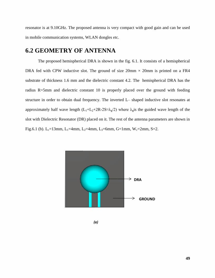
The proposed hemispherical DRA is shown in the fig. 6.1. It consists of a hemispherical
DRA fed with CPW inductive slot. The ground of size 20mm × 20mm is printed on a FR4
substrate of thickness 1.6 mm and the dielectric constant 4.2. The hemispherical DRA has the
radius R=5mm and dielectric constant 10 is properly placed over the ground with feeding
structure in order to obtain dual frequency. The inverted L– shaped inductive slot resonates at
approximately half wave length (L1+L2+2R-2S≈λg/2) where λgis the guided wave length of the
slot with Dielectric Resonator (DR) placed on it. The rest of the antenna parameters are shown in
Fig.6.1 (b). Lc=13mm, L1=4mm, L2=4mm, L3=6mm, G=1mm, Wc=2mm, S=2.
(a)
DRA
GROUND

50
(b)
Fig.6.1. Proposed antenna (a) Front view (b) Feed geometry
6.3 SIMULATION SETUP AND RESULTS
6.3.1 Simulation Setup
The commercial 3D full wave electromagnetic (EM) simulation software CST
Microwave studio is used for simulation. It analyzes 3D and multilayer structures of general
shapes. It has been widely used in the design of MICs, RFICs, patch antennas, wire antennas,
and other RF/wireless antennas. It can be used to calculate and Return loss plot, VSWR, current
distributions, radiation patterns etc.
6.3.2 Return loss and Antenna Bandwidth
As described in chapter three, the bandwidth can be calculated from the return loss (RL)
plot. The bandwidth of the antenna is said to be those range of frequencies over which the return
L1
L2
L3
LC
20 mm
20 mm
wC
G

51
loss is less than -10dB, which is equivalent to 2:1 VSWR. Several structures of feeding design
was considered found changing the length of L2 and L3 and found that this feed design is
optimum .The proposed antenna resonates at the dual frequency. The lower band is due to the
CPW inductive slot while the higher band is due to the DR. The simulated lower band achieves
impedance bandwidth of 18.63% (for S11<-10 dB) from the Return loss graph shown in the Fig.
6.2. Ranging from 2.2 to 2.65 GHz with center frequency at 2.42GHz and the higher band
achieves band width of 7% with center frequency at 9.13 GHz.
Fig.6.2. Simulated Return loss of the proposed antenna
6.3.3 Current distribution in the antenna
The current distribution shown in the Fig.6.3. Shows that at 2.4GHz total current is
distributed across the inductive slot and the slot resonates at that frequency at 9GHz the current
is totally distributed across the DR thus it gives the higher resonant frequency and dual is
obtained.
Frequency (GHz)
Ret
urn
loss
(d
B)

52
(a)
(b)
Fig 6.3. Current distribution at (a) 2.4GHz (b) 9GHz
6.3.4 Gain vs. Frequency Plot
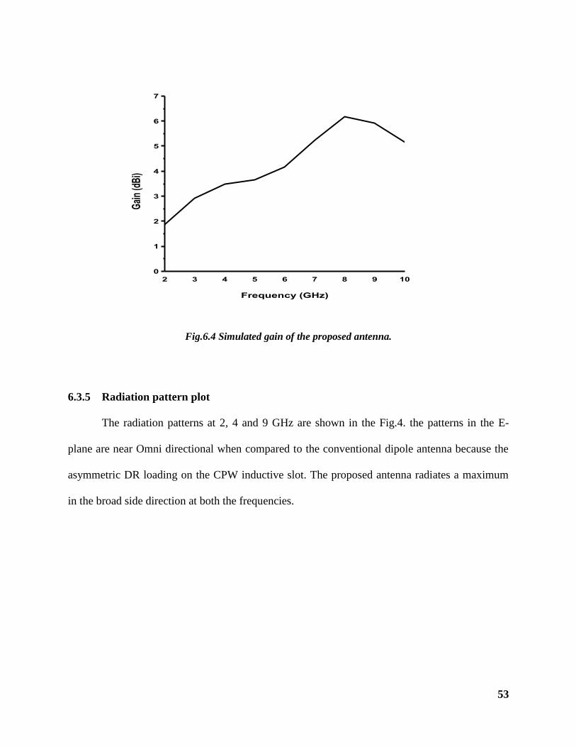
The gain vs. frequency graph shown in the Fig. 6.4. Shows that the gain at 2.4GHz is
2.36dBi and 9GHz it is 5.91dBi.
53
2 3 4 5 6 7 8 9 10
0
1
2
3
4
5
6
7
Gai
n (d
Bi)
Frequency (GHz)
Fig.6.4 Simulated gain of the proposed antenna.
6.3.5 Radiation pattern plot
The radiation patterns at 2, 4 and 9 GHz are shown in the Fig.4. the patterns in the E-
plane are near Omni directional when compared to the conventional dipole antenna because the
asymmetric DR loading on the CPW inductive slot. The proposed antenna radiates a maximum
in the broad side direction at both the frequencies.

54
E-Plane H-Plane
Fig.6.5. Radiation pattern at 2.4 GHz and 9GHz.

55
6.4 PRACTICAL ANTENNA
When the same above proposed antenna is designed with dielectric constant of 2.1 the
resonant frequency is shifted to 3.6GHz
Fig.6.6 Practical antenna with dielectric constant 2.1
Fig. 6.6.1 simulated Return loss
For practical purpose when hemispherical DRA is replaced with square DRA for ease of
fabrication with dimensions 5mm x 5mmthe resonant frequency is showing as 3.6GHz as per the
return loss graph. Which means that shape of DRA is not effecting the resonant frequency , only
the dielectric constant has major effect on the resonant frequency.i.e., when dielectric constant is
10 resonant frequency is 2.42 GHz an when it is lower to 2.1 the resonant frequency shifted to
higher frequency at 3.6GHz.
S in
dB

56
Fig.6.7 Practical antenna with dielectric constant 2.1 and square DRA
Fig. 6.7.1 simulated Return loss
Fig. 6.7.2 Fabricated antenna
S in
dB

57
Fig. 6.7.3 Measured return loss
CONCLUSION
Compact hemispherical DRA with dielectric constant of 10 was designed and simulated.
Due to advantages of CPW feeding like low radiation leakages, less dispersion, this CPW
feeding is used for this antenna. This antenna resonates at two different frequencies one at
2.42GHz and other at 9.13GHz. The proposed antenna is fabricated with dielectric constant of

58
2.1 and DRA with square shape and measured return loss shows that due to lesser dielectric
constant the resonant frequency is shifted to 3.6GHZ which is used for WiMAX.

59
CHAPTER
7
CONCLUSION
AND
FUTURE SCOPE

60
7.1 CONCLUSION
In these thesis three different dielectric resonator antennas for short range wireless
communication application has been designed. Ultra-wide band (UWB) and WLAN are popular
research and commercial topics for short range wireless communication.
In chapter 4 dielectric resonator antenna for UWB has been designed. The antenna
simulations shows indicated the best results in the gain and return loss. The path loss is almost
constant when two antennas are placed face to face and slightly distorted when placed side by
side and the variation of the Group delay is less than 1ns. in the operating frequency band. From
the results we can expect that the characteristic of far field phase is linear in UWB frequency
band and pulse communication will be possible.
In chapter 5 dielectric resonator antenna for WLAN which operates at 5.5GHz is
designed. A microstrip feed line with a rectangular patch which has input impedance of 50 Ω is
used for matching.The rectangular patch- feed mechanism gives good coupling between the
patch and DR.The antenna simulations shows indicated the best results in the gain which is
above 6dBi in the range of 5-6GHz band and return loss is -22.7dB at 5.5GHz and the
radiationpattern is showing that this antenna can be used as Omni directional antenna.
In chapter 6 compact hemispherical DRA with dielectric constant of 10 was designed
and simulated. Due to advantages of CPW feeding like low radiation leakages, less dispersion,
this CPW feeding is used for this antenna. This antenna resonates at two different frequencies
one at 2.42GHz and other at 9.13GHz. The proposed antenna is fabricated with dielectric
constant of 2.1 and DRA with square shape and measured return loss shows that due to lesser
dielectric constant the resonant frequency is shifted to 3.6GHZ which is used for WiMAX.

61
FUTURE SCOPE
Fabrication of UWB antenna with dielectric constant 10.2 and measurement is to be done. While
designing UWB antenna time domain characteristics, path loss and group delay is to be
considered. For other applications like WLAN higher the dielectric constant lower the resonant
frequency, as dielectric constant is reduced the resonant frequency shifts to higher frequencies.
PUBLICATIONS
[1]P. Mahender, S. Natarajamani, S.K. Behera, “H-Shaped Dielectric Resonator Antenna for
UWB application”, International Symposium on Devices,MEMS, Intelligent System and
Communication System,12-14 April 2011, Sikkim, India.
[2] P. Mahender, S. Natarajamani, S.K. Behera, “Inverted U-Shaped Dielectric Resonator
Antenna for WLAN”,Proceedings of the 2010 IEEE International Conference on
Communication, Control and Computing Technologies.
[3] P. Mahender, RunaKumari, S.K. Behera, “Compact Dual Band Hemi Spherical
DielectricResonator Antenna”, International Conference on Electronic Systems (ICES-2011), 7-9
Jan 2011, NIT Rourkela, India.
62
REFERENCES
[1] Petosa, A., Dielectric Resonator Antenna Handbook, Artech House, 2007.
[2] First Report and Order , Federall Communications(FCC), Feb. 2002.
[3] M. Z. Win, R. A. Scholtz, and M. A. Barnes, “Ultra-wide bandwidth signal propagation for indoor
wireless communications,” in Proc. IEEE Int. Conf. Commun., Vol. 1,June 1997, pp. 56-60.
[4] R. J. Cramer, R. A. Scholtz, and M. Z. Win,”Evalution of an Ultra-wide-band propagation channel,”
IEEE Trans. Antennas Propagat., Vol. 50, pp. 561-570, may 2002.
[5] M. Welborn and J.McCorkle, ”The importance of fractional band-width in ultra-wideband pulse design,”
in IEEE Int. Conf. Commun.(ICC2002), Vol. 2, 2002, pp. 753-757.
[6] M. Z. Win and R. A. Scholtz, “On the robustness of Ultra-wide band-width signals in dense multipath
environments,”IEEE Commun. Lett.,Vol. 2, pp. 51-53, Feb. 1998.
[7] S. A. Long, M. W. McAllister, and L. C. Shen, “The resonant cylindrical dielectric cavity antenna,” IEEE
Transactions Antenna and Propagations,Vol. 31, pp. 406-412, 1983.
[8] Ying-Ying Yang, Qing-Xin Chu, and Zhi-An Zheng, “Time Domain Characteristics of Band-Notched
Ultrawideband Antenna,” IEEE Transactions on Antennas and Propagation,Vol. 57, No. 10, Oct. 2009.
[9] Kenny Seungwoo Ryu, Ahmed A. Kishk, “Ultra-Wide Band Dielectric Resonator Antenna with
Broadside Patterns Mounted on a Vertical Ground Plane Edge,”IEEE Transactions on Antennas and
Propagation, Vol. 58, No. 4, APRIL 2010.
[10] Jung N. Lee, Ji H. Kim, Jong K. Park, and Jin S.Kim, ”Design of Dual-Band Antenna with U-Shaped
open stub for WLAN/UWB Applications,” Microwave and Optical Technology Letters/ Vol. 51, No. 2,
February 2009.
[11] A.Kishk “Dielectric resonator Antenna, a candidate for radar applications”, proc. Of the 2003 Radar
conference, pp. 258-264, May 2003.
[12] P. Rezaei M.Hakkak and K.Forooraghi “ Dielectric resonator antenna for wireless lan applications”,IEEE
Antennas and propagation society symposium, Vol. 2, pp. 1005-1008, July 2006.

63
[13] M.F Ain , S.I.S. Hassan,M.A.Othman, S.Sreekanthan,S.D.Hutagalug and Z.A.Ahmed. “wideband
dielectric resonator antenna for C Band application”,International conference on computer and
Communication Engineering 2008(ICCCE 2008), pp. 997-999, MAY 2008.
[14] A.Petosa, A.Ittipiboon, Y.M.M Antar1, D.Roscoe, and M.Cuhaci, IEEE Antennas and Propagation
Magazine, Vol. 40, No. 3, pp. 35-48, June 1998
[15] Long, S. A., M. W. McAllister, and L. C. Shen, “Rectangular dielectric resonator antenna,” IEEE
Electronics Letters, Vol. 19, 218-219, Mar. 1983.
[16] Kranenburg, R. A. and S. A. Long, “Microstrip transmission line excitation of dielectric resonator
antennas,” IEEE Electronics Letters, Vol. 24, No. 18, 1156-1157,Sep.1988.
[17] Makwana, G. D. and K. J. Vinoy, “A microstrip line fed rectangular dielectric resonator antenna for
WLAN application,” Proceeding of IEEE International symposium on Microwave, 299-303, Dec. 2008.
[18] Martin, J. T. H. ST. and Y. M. M. Antar, “Dielectric resonator antenna using aperture coupling,” IEEE
Electronics Letters, Vol. 26, No. 24, 2015-2016, Nov. 1990.
[19] Kranenburg, R. A., S. A. Long, and J. T. Williams, “Coplanar waveguide excitation of dielectric
resonator antenna,” IEEE Transaction on Antennas and Propagation, Vol. 39, 119-122, Jan. 1991.
[20] R.K.Mongia and A.Ittipiboon, “Theoretical and experimental investigations on rectangular dielectric
resonator antennas,” IEEE Transactions on Antennas and Propagation, vol. 45, no.9, pp. 1348-1356,
September 1997.
[21] Xian-Ling Liang and Tayeb A.Denidni, “H-Shaped Dielectric Resonator Antenna for Wideband
Applications”, IEEE Antennas and Wireless propagation letters, Vol.7, pp. 163-166, Feb 2008.
[22] Aldo Petosa, Dielectric Resonator Antenna Handbook,Artech house.K.M. Luk, and K.W. Leung,
Dielectric Resonator Antennas, Hertfordshire, England, Research studies Press
[23] Deidni, T. A., and Rao, “Hybrid dielectric resonator antenna with radiating slot for dual-frequency
operation”,IEEE Antennas and Wireless propgat. Letters,2004, 3, pp. 321-323.

64
[24] A.B.Buerkie, K. Sarabandi, and H.Mosllaei, “compact slot and dielectric resonator antenna with dual-
resonance , broadband characteristics”, IEEE Trans. Antennas Propagat., Vol. 53, no. 3, pp.1020-1027,
2005.
[25] Q.Rao, T.A. Denidni, A.R.Sebak. and R.H. Johnson, “compact independent dual-band hybrid resonator
antenna with multifunctional beams,” IEEE Antennas and Wireless Propagat.Letters, Vol.5, pp. 239-242,
2006.
[26] Z.N.Chen, K.Hirasawa, K.W.Leung,and K.M.Luk, “A new inverted antenna with a ring dielectric
resonator” IEEE Trans .Vehicular Technology, Vol. 48, no. 4, pp. 1029-1032, 1999.
[27] K.P. Esselle, and T.S. Bird, “ A hybrid –resonator antenna experimental results,” IEEE Trans. Antennas
Propgat., Vol. 53, no. 2, pp.870-871, 2005.
[28] K.Lan, S.K. Chaudhuri, and S. Safavi-Naeini, “design and analysis of a combination antenna with
rectangular dielectric resonator and inverted L-plate,” IEEE Trans. Antennas Propgat., Vol.53, no. 1, pp.
495-501, 2005.
[29] Y. Gao, B.L. Ooi, W.B.Ewe, and A.P.Popov, “ A compact wideband hybrid dielectric resonator antenna
,” IEEE Microwave Wireless Components Lett.., Vol. 16, no. 4, pp. 227-229, 2006.
[30] Y. Gao, A.P. Popov, and B.L. Ooi “ Experimental study of wideband hybrid dielectric resonator antenna
on small ground plane,” Electron Lett., Vol. 42, no. 13, 2006.
[31] J. Janapsatya, K.P. Esselle, and T.S. Bird, “ Compact wideband dielectric-resonator –on-patch antenna,”
Electron Lett., Vol. 42, no. 19, 2006.
[32] K.K. So, and K.W. Leung, “ Bandwidth enhancement and frequency tuning of the dielectric resonator
antenna using a parasitic slot in the ground plane,” IEEE trans. Antennas propgat., Vol. 53, no. 12, pp.
4169-4172, 2005
[33] Hua-Ming Chen, Yi-Fang Lin, Chia-Ho Lin, Shih-Chieh Lin, “ Compact dual-band hybrid dielectric
resonator antenna,” Tencon 2007, IEEE region 10 conference.

65


![ANTENNA BEHAVIOUR UNDER DIFFERENT SOIL CONDITIONS...[21] Varun Shukla, Arti Saxena and Swati Jain, A New Rectangular Dielectric Resonator Antenna Compatible for Mobile Communication](https://img.pdfslide.us/doc/110x75/5f935e7cb3469a48e978d7c8/antenna-behaviour-under-different-soil-21-varun-shukla-arti-saxena-and-swati.jpg)