Embed Size (px)
Citation preview
AN10935Using SDR/DDR SDRAM memories with LPC32xx
Rev. 2 — 11 October 2010 Application note
Document information
Info Content
Keywords LPC32x0, LPC32xx, LPC3220, LPC3230, LPC3240, LPC3250, SDR, SDRAM, DDR
Abstract This application note covers hardware related issues for interfacing SDR or DDR SDRAMs to the LPC32xx family microcontroller.
NXP Semiconductors AN10935 Using SDR/DDR SDRAM memories with LPC32xx
AN10935 All information provided in this document is subject to legal disclaimers. © NXP B.V. 2010. All rights reserved.
Application note Rev. 2 — 11 October 2010 2 of 47
Contact informationFor additional information, please visit: http://www.nxp.com For sales office addresses, please send an email to: [email protected]
Revision history
Rev Date Description
2 20101011 • Add Section 2.4. • Updated Table 6. • Updated Table 7.
1 20100603 Initial version
NXP Semiconductors AN10935 Using SDR/DDR SDRAM memories with LPC32xx
1. Introduction NXP’s LPC32x0 32-bit microcontroller was designed for embedded applications requiring high performance and low power consumption. The LPC32x0 is based on the ARM926EJ-S CPU core with a Vector Floating Point co-processor, and a large set of standard peripherals. The basic ARM926EJ-S CPU Core implementation uses Harvard architecture with a 5-stage pipeline, and has one 32 kB instruction cache and one 32 kB data cache. The ARM926EJ-S core also has an integral Memory Management Unit (MMU) to provide the virtual memory capabilities required to support the multi-programming demands of modern operating systems. The LPC32x0 comes with internal static memory ranging between 128 kB to 256 kB. While this is enough memory for some embedded applications, many applications require larger amounts of memory. The LPC32x0 has an integrated External Memory Controller (EMC) for interfacing to external memories.
The LPC32x0 EMC is an ARM PrimeCell MultiPort Memory Controller peripheral offering support for asynchronous static memory devices such as RAM, ROM and Flash, as well as dynamic memories such as Single Data Rate (SDR) and Double Data Rate (DDR) SDRAM. For external memory of 2 MB or larger the most practical memories to use today are SDR or DDR SDRAM.
This application note will focus on connectivity, initialization and board layout guidelines when using SDR and DDR memories with the LPC32x0.
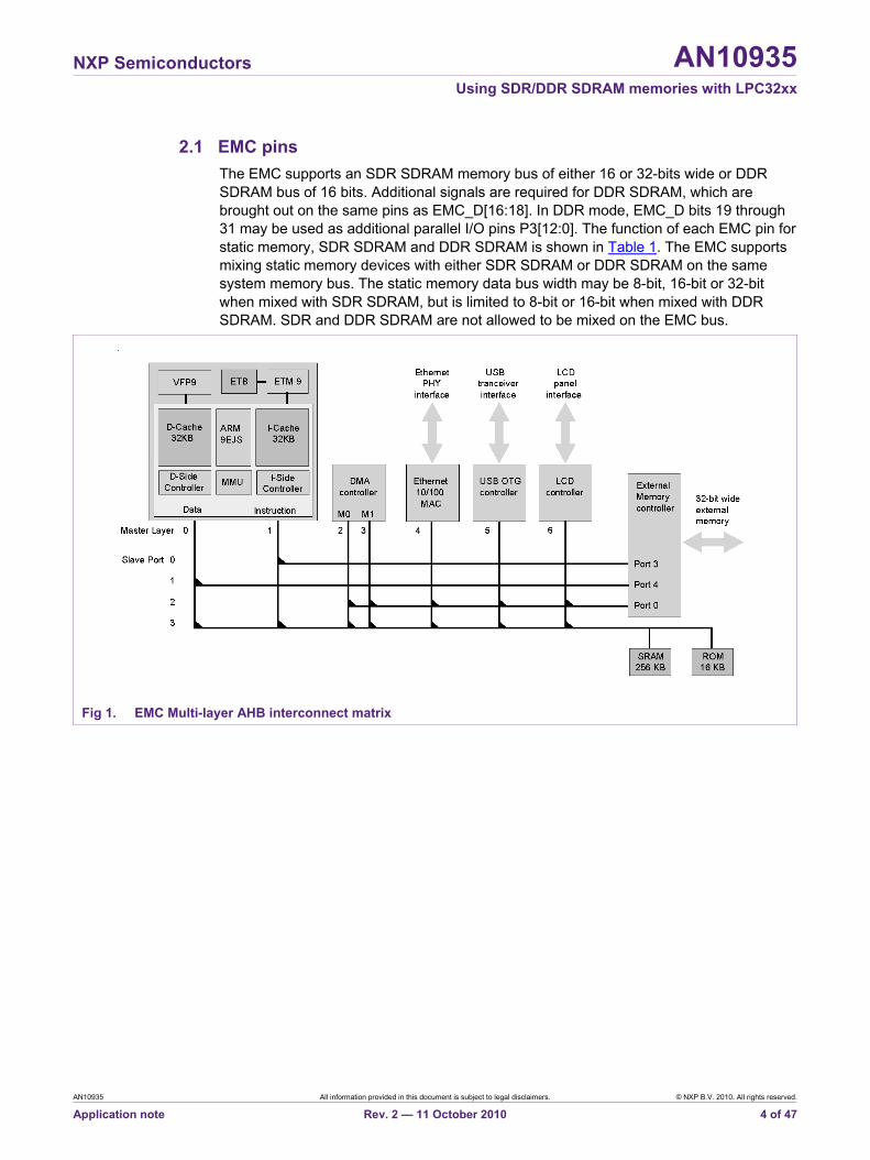
2. External memory controller The LPC32x0 uses an expanded AMBA high-performance bus (AHB) architecture known as Multi-layer AHB. A Multi-layer AHB replaces the request/grant and arbitration mechanism used in a simple AHB with an interconnect matrix that moves arbitration out toward the slave devices. Within the interconnect matrix each slave port has its own arbitration block. Thus, if a CPU and a DMA controller want access to the same memory, the interconnect matrix arbitrates between the two when granting access to the memory. The LPC32x0 has seven AHB masters: the CPU data bus, CPU instruction bus, two general purpose DMA masters, Ethernet controller, USB controller, and LCD controller. The AHB masters access external memory through the EMC on one of three AHB slave ports. A block diagram of how the LPC32x0 bus masters connect to the EMC through the Multi-layer AHB interconnect matrix is shown in Fig 1. The EMC translates AHB master requests on the slave AHB ports for access to external memory into commands and data transactions that follow the selected memory protocol.
AN10935 All information provided in this document is subject to legal disclaimers. © NXP B.V. 2010. All rights reserved.
Application note Rev. 2 — 11 October 2010 3 of 47
NXP Semiconductors AN10935 Using SDR/DDR SDRAM memories with LPC32xx
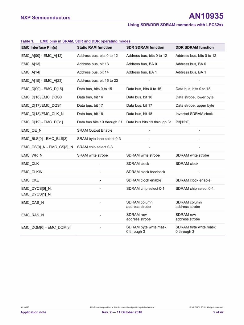
2.1 EMC pins The EMC supports an SDR SDRAM memory bus of either 16 or 32-bits wide or DDR SDRAM bus of 16 bits. Additional signals are required for DDR SDRAM, which are brought out on the same pins as EMC_D[16:18]. In DDR mode, EMC_D bits 19 through 31 may be used as additional parallel I/O pins P3[12:0]. The function of each EMC pin for static memory, SDR SDRAM and DDR SDRAM is shown in Table 1. The EMC supports mixing static memory devices with either SDR SDRAM or DDR SDRAM on the same system memory bus. The static memory data bus width may be 8-bit, 16-bit or 32-bit when mixed with SDR SDRAM, but is limited to 8-bit or 16-bit when mixed with DDR SDRAM. SDR and DDR SDRAM are not allowed to be mixed on the EMC bus.
Fig 1. EMC Multi-layer AHB interconnect matrix
AN10935 All information provided in this document is subject to legal disclaimers. © NXP B.V. 2010. All rights reserved.
Application note Rev. 2 — 11 October 2010 4 of 47
NXP Semiconductors AN10935 Using SDR/DDR SDRAM memories with LPC32xx
Table 1. EMC pins in SRAM, SDR and DDR operating modes EMC Interface Pin(s) Static RAM function SDR SDRAM function DDR SDRAM function
EMC_A[00] - EMC_A[12] Address bus, bits 0 to 12 Address bus, bits 0 to 12 Address bus, bits 0 to 12
EMC_A[13] Address bus, bit 13 Address bus, BA 0 Address bus, BA 0
EMC_A[14] Address bus, bit 14 Address bus, BA 1 Address bus, BA 1
EMC_A[15] - EMC_A[23] Address bus, bit 15 to 23 - -
EMC_D[00] - EMC_D[15] Data bus, bits 0 to 15 Data bus, bits 0 to 15 Data bus, bits 0 to 15
EMC_D[16]/EMC_DQS0 Data bus, bit 16 Data bus, bit 16 Data strobe, lower byte
EMC_D[17]/EMC_DQS1 Data bus, bit 17 Data bus, bit 17 Data strobe, upper byte
EMC_D[18]/EMC_CLK_N Data bus, bit 18 Data bus, bit 18 Inverted SDRAM clock
EMC_D[19] - EMC_D[31] Data bus bits 19 through 31 Data bus bits 19 through 31 P3[12:0]
EMC_OE_N SRAM Output Enable - -
EMC_BLS[0] - EMC_BLS[3] SRAM byte lane select 0-3 - -
EMC_CS[0]_N - EMC_CS[3]_N SRAM chip select 0-3 - -
EMC_WR_N SRAM write strobe SDRAM write strobe SDRAM write strobe
EMC_CLK - SDRAM clock SDRAM clock
EMC_CLKIN - SDRAM clock feedback -
EMC_CKE - SDRAM clock enable SDRAM clock enable
EMC_DYCS[0]_N, EMC_DYCS[1]_N
- SDRAM chip select 0-1 SDRAM chip select 0-1
EMC_CAS_N - SDRAM column address strobe
SDRAM column address strobe
EMC_RAS_N - SDRAM row address strobe
SDRAM row address strobe
EMC_DQM[0] - EMC_DQM[3] - SDRAM byte write mask 0 through 3
SDRAM byte write mask 0 through 3
AN10935 All information provided in this document is subject to legal disclaimers. © NXP B.V. 2010. All rights reserved.
Application note Rev. 2 — 11 October 2010 5 of 47
NXP Semiconductors AN10935 Using SDR/DDR SDRAM memories with LPC32xx
2.2 Maximum system SDRAM memory The LPC32x0 supports two dynamic memory chip selects, EMC_DYCS[1:0]_N. Each chip select addresses 512 MB. However, the largest density SDRAM device supported by the EMC is limited by 13 row address bits (8K rows), making the largest compatible SDRAM devices the 1 Gbit device configured as 32M x 32 or 512 Mbit configured as 16M x 32, 32M x 16 or 64M x 8. Using these compatible SDRAM configurations the maximum amount of SDRAM that can be physically supported per chip select is limited to 256 MB, 128 MB or 64 MB depending on the data width of the SDRAM device(s) and the total bus width of the system memory. The LPC32xx EMC supports a 32-bit system memory bus for SDR, but supports only a 16-bit system memory bus for DDR. Using DDR will limit the memory to half that of a comparable SDR system. Mobile SDR and Mobile DDR SDRAM devices are not produced in x8 data width, hence using Mobile/Low Power SDRAM (1.8 V) will limit the system memory to half that of a comparable standard SDRAM (2.5 V/3.3 V) system. The maximum SDR memory configurations per chip select is shown in Table 2 , and the maximum DDR configurations per chip select are shown in Table 3. A system using both chip selects will support twice the memory listed in Table 2 or Table 3. The SDRAM address ranges are shown using x8, x16 and x32 memory devices in Table 4.
Table 2. Maximum SDR SDRAM per chip select 32-bit System Memory SDR SDRAM
Memory type Example SDRAM SDRAM density Devices used
Maximum memory
Standard (3.3 V) MT48LC64M8A2P 512 Mbit (64M x 8) 4 256 MB
Low power (1.8 V)
MT48H32M16LFBF 512 Mbit (32M x 16)
2 128 MB
Low power (1.8 V)
H55S1G22MFP 1 Gbit (32M x 32) 1 128 MB
16-bit System Memory SDR SDRAM
Memory type Example SDRAM SDRAM density Devices used
Maximum memory
Standard (3.3 V) MT48LC64M8A2P 512 Mbit (64M x 8) 2 128 MB
Low power (1.8 V)
MT48H32M16LFBF 512 Mbit (32M x 16)
1 64 MB
Table 3. Maximum DDR SDRAM per chip select 16-bit System Memory DDR SDRAM
Memory type Example SDRAM SDRAM density Devices used Maximum memory
Standard (2.5 V) MT46V64M8P 512 Mbit (64M x 8) 2 128 MB
Low power (1.8 V)
MT46H32M16LFBF 512 Mbit (32M x 16)
1 64 MB
AN10935 All information provided in this document is subject to legal disclaimers. © NXP B.V. 2010. All rights reserved.
Application note Rev. 2 — 11 October 2010 6 of 47
NXP Semiconductors AN10935 Using SDR/DDR SDRAM memories with LPC32xx
Table 4. Physical SDRAM address mapping Chip select AHB Address Address range
X16 System data bus Address range X32 System data bus (SDR only)
512 Mbit SDRAM (32M x 16)
512 Mbit SDRAM (64M x 8)
512 Mbit SDRAM (16M x 32)
512 Mbit SDRAM (32M x 16)
512 Mbit SDRAM (64M x 8)
64 MB 128 MB 64 MB 128 MB 256 MB
EMC_DYCS[1]_N 0xBFFF FFFF 0xA000 0000
0xA3FF FFFF 0xA000 0000
0xA7FF FFFF 0xA000 0000
0xA3FF FFFF 0xA000 0000
0xA7FF FFFF 0xA000 0000
0xAFFF FFFF 0xA000 0000
EMC_DYCS[0]_N
0x9FFF FFFF 0X8000 0000
0x83FF FFFF 0x8000 0000
0x87FF FFFF 0x8000 0000
0x83FF FFFF 0x8000 0000
0x87FF FFFF 0x8000 0000
0x8FFF FFFF 0x8000 0000
2.3 Contiguous SDRAM across EMC_DYCS0 and EMC_DYCS1 Sometimes to have enough system memory both EMC_DYCS0 and EMC_DYCS1 must be used. Since the physical SDRAM addressing range will always be smaller than the AHB address range allotted to EMC_DYCS0, as shown in Table 4, the physical SDRAM will have mirrored address ranges across the full EMC_DYCS0 space. To make the memory appear contiguous the EMC_DYCS0 SDRAM can be addressed at the largest mirrored address space. For example if a 32Mx16 Mobile DDR were placed on each EMC_DYCSx, the contiguous address range for the combined memories would be 0x9C00 0000 to 0xA3FF FFFF.
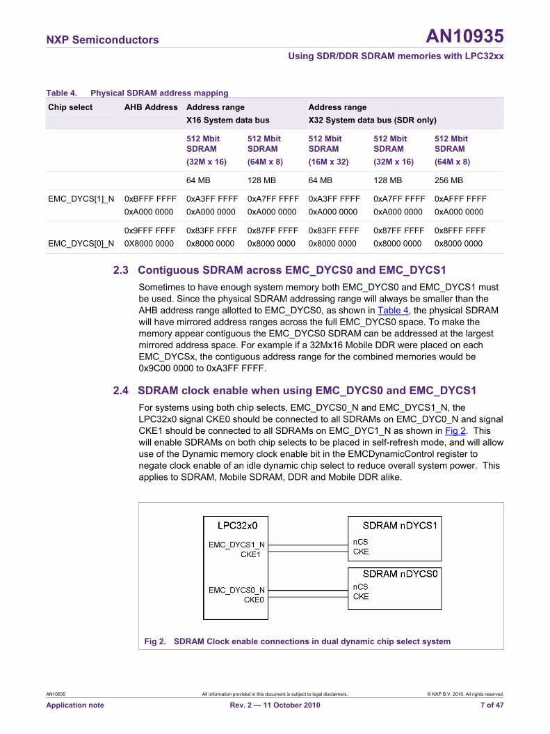
2.4 SDRAM clock enable when using EMC_DYCS0 and EMC_DYCS1 For systems using both chip selects, EMC_DYCS0_N and EMC_DYCS1_N, the LPC32x0 signal CKE0 should be connected to all SDRAMs on EMC_DYC0_N and signal CKE1 should be connected to all SDRAMs on EMC_DYC1_N as shown in Fig 2. This will enable SDRAMs on both chip selects to be placed in self-refresh mode, and will allow use of the Dynamic memory clock enable bit in the EMCDynamicControl register to negate clock enable of an idle dynamic chip select to reduce overall system power. This applies to SDRAM, Mobile SDRAM, DDR and Mobile DDR alike.
Fig 2. SDRAM Clock enable connections in dual dynamic chip select system
AN10935 All information provided in this document is subject to legal disclaimers. © NXP B.V. 2010. All rights reserved.
Application note Rev. 2 — 11 October 2010 7 of 47
NXP Semiconductors AN10935 Using SDR/DDR SDRAM memories with LPC32xx
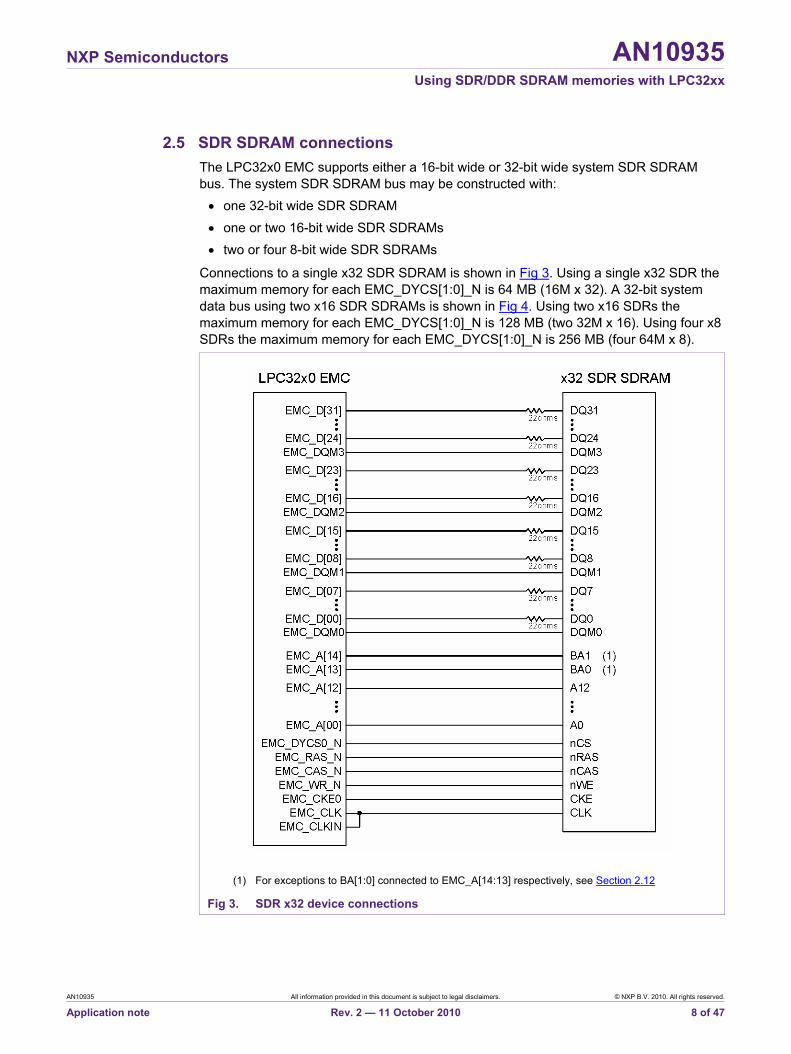
2.5 SDR SDRAM connections The LPC32x0 EMC supports either a 16-bit wide or 32-bit wide system SDR SDRAM bus. The system SDR SDRAM bus may be constructed with:
• one 32-bit wide SDR SDRAM • one or two 16-bit wide SDR SDRAMs • two or four 8-bit wide SDR SDRAMs
Connections to a single x32 SDR SDRAM is shown in Fig 3. Using a single x32 SDR the maximum memory for each EMC_DYCS[1:0]_N is 64 MB (16M x 32). A 32-bit system data bus using two x16 SDR SDRAMs is shown in Fig 4. Using two x16 SDRs the maximum memory for each EMC_DYCS[1:0]_N is 128 MB (two 32M x 16). Using four x8 SDRs the maximum memory for each EMC_DYCS[1:0]_N is 256 MB (four 64M x 8).
(1) For exceptions to BA[1:0] connected to EMC_A[14:13] respectively, see Section 2.12
Fig 3. SDR x32 device connections
AN10935 All information provided in this document is subject to legal disclaimers. © NXP B.V. 2010. All rights reserved.
Application note Rev. 2 — 11 October 2010 8 of 47
NXP Semiconductors AN10935 Using SDR/DDR SDRAM memories with LPC32xx
(1) For exceptions to BA[1:0] connected to EMC_A[14:13] respectively, see Section 2.12
Fig 4. SDR x16 device connections
2.5.1 Routing rules for SDR SDRAM When using multiple SDR SDRAM configurations it is best to place all memories near each other and route address, control and clock signals in a “Y” topology. Keep as much of the overall trace length in the trunk of the “Y” as possible, and the length to each device after the split as short as possible. Match the trace length to each device to within 0.3”.
Rule 1: match EMC_Data[7:0], EMC_DQM0 to within 0.3 inches of each other.
Rule 2: match EMC_Data[15:8], EMC_DQM1 to within 0.3 inches of each other.
Rule 3: match EMC_Data[23:16], EMC_DQM2 to within 0.3 inches of each other.
Rule 4: match EMC_Data[31:24], EMC_DQM3 to within 0.3 inches of each other.
Rule 5: match signal groups from rule 1 through rule 4 to within 1.0 inches of each other.
Rule 6: match EMC_CLK to within +-0.30 inches of signal groups rule 1 through rule 4.
Rule 7: match EMC_A[14:0], EMC_RAS, EMC_CAS, EMC_DYCS[1:0]_N, EMC_WR_N, EMC_CKE[1:0] to within +- 0.500 inches of EMC_CLK.
AN10935 All information provided in this document is subject to legal disclaimers. © NXP B.V. 2010. All rights reserved.
Application note Rev. 2 — 11 October 2010 9 of 47
NXP Semiconductors AN10935 Using SDR/DDR SDRAM memories with LPC32xx
2.5.2 Function of EMC_CLKIN pin The EMC_CLKIN pin is the MPMC data-in-clock during SDR SDRAM reads. After a SDR SDRAM read command is issued, the MPMC will latch burst data on the rising edge of EMC_CLKIN after the number of CAS latency clock cycles has elapsed (see UM EMCDynamicRasCas). An external clock pin provides a way to compensate for signal flight delay times when the SDR SDRAM is placed far enough from the LPC32x0 that data being read does not arrive in time to meet the EMC SDR SDRAM tsu(D) data input set-up time for the tck EMC_CLK period. Most embedded system designs can tie EMC_CLKIN (bga ball T4) directly to the EMC_CLK pin (bga ball T3).
Here’s an example of how long the traces can be before needing to route EMC_CLKIN differently than just connecting directly to the adjacent EMC_CLK pin.
Example Parameters: • SDR SDRAM maximum access time = 5.4 ns (SDRAM datasheet) • LPC32x0 tsu(D) data in set-up time = 0.6 ns • EMC-CLK period tck = 7.5 ns; (133 MHz)
The allowed combined flight time and board signal jitter must be less than the EMC_CLK period minus the combined SDRAM access time and LPC32x0 data in set-up time. Therefore, flight + jitter = 7.5 ns – 6 ns = 1.5 ns. Reserving 300 ps for jitter leaves 1.2 ns for round trip flight time. Assuming the signal travels on the PCB at 167 ps/inch we can have a total trace length of 600 ps/167 ps = 3.6 inches between the LPC32x0 and the SDR SDRAM. The allowable trace length without compensation will increase as the EMC_CLK period increases. With an EMC_CLK period of 9.6 ns (104 MHz), the allowable trace length would be 9.9 inches.
2.5.2.1 EMC_CLKIN to compensate for long flight times
To compensate flight delay times longer than will work for a given tck period and SDR SDRAM access time, the EMC_CLK is split routed with equal length traces to the SDR SDRAM and EMC_CLKIN each with a series source termination, as shown in Fig 5. The series termination resistor value is dependent on the PCB trace characteristic impedance. The 0 ohm termination is used when the trace impedance is near 50 ohms, while 22 ohms is used when trace impedance is near 75 ohms. The extra trace length to EMC_CLKIN compensates for one way signal flight time. So the example above would now meeting timing with up to 7.2 inches of trace length with tck = 7.5 ns.
Fig 5. Compensate signal flight time with EMC_CLKIN
AN10935 All information provided in this document is subject to legal disclaimers. © NXP B.V. 2010. All rights reserved.
Application note Rev. 2 — 11 October 2010 10 of 47
NXP Semiconductors AN10935 Using SDR/DDR SDRAM memories with LPC32xx
2.6 DDR SDRAM connections The LPC32x0 EMC supports only a 16-bit wide system DDR SDRAM bus. The system DDR SDRAM bus may be constructed with:
• one 16-bit wide DDR SDRAM • two 8-bit wide DDR SDRAMs
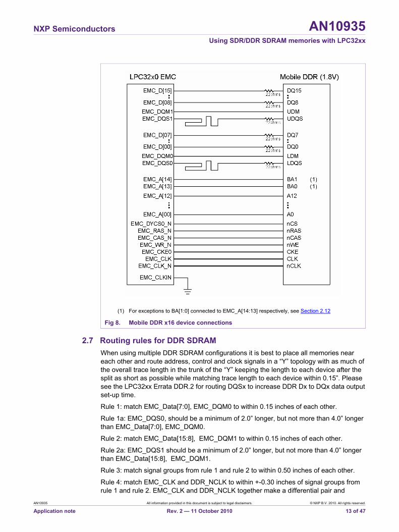
Connections to a single x16 DDR SDRAM are shown in Fig 6. Using a single x16 DDR, the maximum memory for each EMC_DYCS[1:0]_N is 64 MB (32M x 16). A 16-bit system data bus using two x8 DDR SDRAMs is shown in Fig 7. Using two x8 DDRs, the maximum memory for each EMC_DYCS[1:0]_N is 128 MB (two 64M x 8). Connections to a single x16 Mobile DDR SDRAM is shown in Fig 8. Please see the LPC32xx errata DDR.1 for using a single ended clock with 2.5V DDR, and DDR.2 for routing DQSx to increase DDR Dx to DQx data output set-up time. The Errata sheet can be found at http://www.nxp.com/documents/errata_sheet/ES_LPC3250.pdf.
(1) For exceptions to BA[1:0] connected to EMC_A[14:13] respectively, see Section 2.12
Fig 6. DDR x16 device connections
AN10935 All information provided in this document is subject to legal disclaimers. © NXP B.V. 2010. All rights reserved.
Application note Rev. 2 — 11 October 2010 11 of 47
NXP Semiconductors AN10935 Using SDR/DDR SDRAM memories with LPC32xx
(1) For exceptions to BA[1:0] connected to EMC_A[14:13] respectively, see Section 2.12
Fig 7. DDR x8 connections
AN10935 All information provided in this document is subject to legal disclaimers. © NXP B.V. 2010. All rights reserved.
Application note Rev. 2 — 11 October 2010 12 of 47
NXP Semiconductors AN10935 Using SDR/DDR SDRAM memories with LPC32xx
(1) For exceptions to BA[1:0] connected to EMC_A[14:13] respectively, see Section 2.12
Fig 8. Mobile DDR x16 device connections
2.7 Routing rules for DDR SDRAM When using multiple DDR SDRAM configurations it is best to place all memories near each other and route address, control and clock signals in a “Y” topology with as much of the overall trace length in the trunk of the “Y” keeping the length to each device after the split as short as possible while matching trace length to each device within 0.15”. Please see the LPC32xx Errata DDR.2 for routing DQSx to increase DDR Dx to DQx data output set-up time.
Rule 1: match EMC_Data[7:0], EMC_DQM0 to within 0.15 inches of each other.
Rule 1a: EMC_DQS0, should be a minimum of 2.0” longer, but not more than 4.0” longer than EMC_Data[7:0], EMC_DQM0.
Rule 2: match EMC_Data[15:8], EMC_DQM1 to within 0.15 inches of each other.
Rule 2a: EMC_DQS1 should be a minimum of 2.0” longer, but not more than 4.0” longer than EMC_Data[15:8], EMC_DQM1.
Rule 3: match signal groups from rule 1 and rule 2 to within 0.50 inches of each other.
Rule 4: match EMC_CLK and DDR_NCLK to within +-0.30 inches of signal groups from rule 1 and rule 2. EMC_CLK and DDR_NCLK together make a differential pair and
AN10935 All information provided in this document is subject to legal disclaimers. © NXP B.V. 2010. All rights reserved.
Application note Rev. 2 — 11 October 2010 13 of 47
NXP Semiconductors AN10935 Using SDR/DDR SDRAM memories with LPC32xx
should be matched length to within 0.150 inches of each other. Note: please see the LPC32xx Errata DDR.1 for using a single ended clock for 2.5V DDR.
Rule 5: match EMC_A[14:0], EMC_RAS, EMC_CAS, EMC_DYCS[1:0]_N, EMC_WR_N, EMC_CKE[1:0] to within +- 0.500 inches of EMC_CLK.
2.7.1 Function of EMC_CLKIN pin EMC_CLKIN is not used for DDR SDRAM configurations and should be tied to gnd or VDD_EMC.
2.8 SDRAM layout optimization Configuring the system memory using a single chip select for SDRAM instead of two dynamic chip selects will help keep the routing for DQ[31:0], DQM[3:0] and DQS[1:0] signals point to point, a good topology for signal integrity. For example, placing two 512 Mbit (64M x 8) DDR devices on a single chip select for 128 MB of system memory is more desirable than building the same system using two chip selects, each with a 512 Mbit (32M x 16) device.
2.9 Shared bus placement for SDRAM and Static memory devices It is best if the SDR/DDR SDRAM is routed point-to-point between the LPC3250. If the LPC3250 EMC bus is shared between SDRAM and static memory, NOR Flash, or memory mapped IO devices, it is recommended to buffer the static memory and memory mapped IO devices keeping just the SDRAM memory and buffer directly connected to the LPC3250. When it is necessary to have an additional device on the EMC bus it is recommended to place the LPC32xx at one extreme on the bus and the SDRAM at the other extreme. The additional NOR Flash or buffer should be place nearer to the SDRAM and the bus routed in daisy chain fashion with stubs no longer than 0.3”.
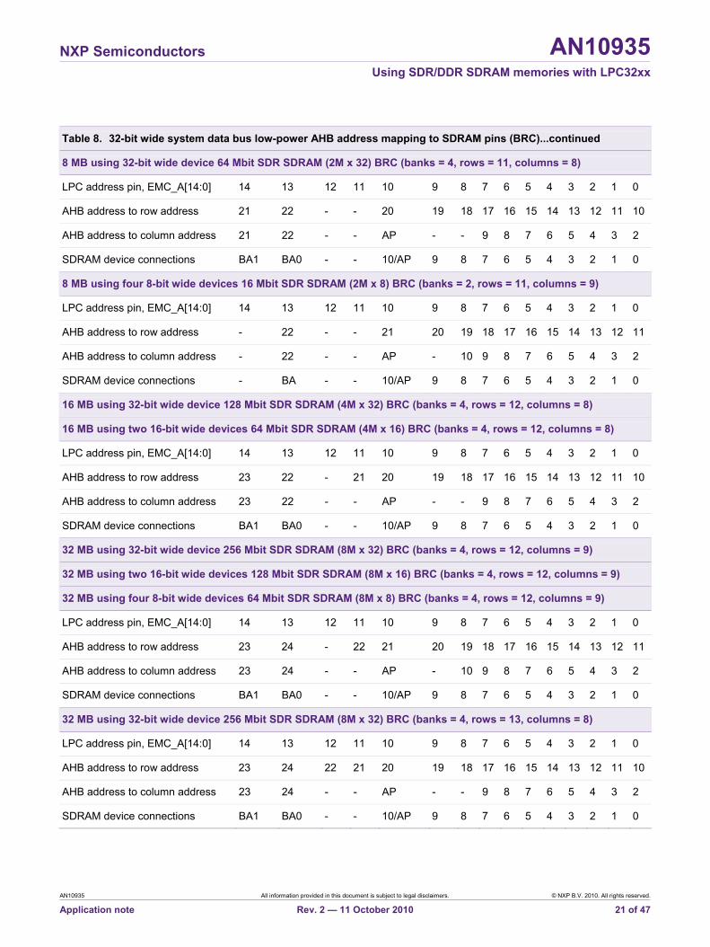
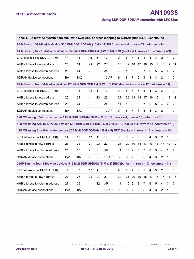
2.10 Address mapping between AHB address and SDR/DDR SDRAM The SDRAM memory is arranged in a XY grid pattern of rows and columns. First, the row address is sent to the memory chip and latched, then the column address is sent in a similar fashion. This row and column-addressing scheme (called multiplexing) allows a large memory address to use fewer pins. The EMC uses EMCDynamicConfig register Address Mapping (AM) field to map the AHB address for a specific SDRAM bank, row and column configuration. The value for the EMCDynamicConfig AM field, for each SDRAM configuration, is found in the LPC32xx User Manual “UM10326” Table 115 Address mapping. The EMC uses the AM field bits 13:12 to determine the order in which the SDRAM bank, row and column address bits are mapped to the AHB address bits. The EMC will always map the least significant AHB address bits to the SDRAM column address. When the AM field bits 13:12 = 0b01 (low-power mapping) the SDRAM row address is mapped to the next significant group of AHB address bits and the SDRAM bank address bits are mapped to the most significant AHB address bits. This is also referred to as Bank-Row-Column (BRC) mapping. When AM field bits 13:12 = 0b00 (high performance mapping) the SDRAM bank address bits are mapped to the next significant AHB address bits after the column address and the SDRAM row address is mapped to the most significant AHB address bits. This is also referred to as Row-Bank-Column (RBC) mapping. The detailed AHB address mapping for 16-bit system memory data bus is shown in Table 5 and Table 6. The detailed AHB address mapping for 32-bit system memory data bus is shown in Table 7 and Table 8. Each EMC_DYNCS[1:0]_N has its own EMCDynamicConfig register, so each chip select may use a different SDRAM
AN10935 All information provided in this document is subject to legal disclaimers. © NXP B.V. 2010. All rights reserved.
Application note Rev. 2 — 11 October 2010 14 of 47
NXP Semiconductors AN10935 Using SDR/DDR SDRAM memories with LPC32xx
density with different row and column configuration. The MPMC maps the SDRAM Auto precharge bit to EMC_A10 during SRAM read, write and precharge commands.
Table 5. 16-bit wide system data bus high performance AHB address mapping to SDRAM pins (RBC) 16-bit wide system data bus high performance AHB address mapping to SDRAM pins (Row, Bank, Column)
2 MB using 16-bit wide device 16 Mbit SDR/DDR SDRAM (1M x 16) RBC (banks = 2, rows = 11, columns = 8)
LPC address pin, EMC_A[14:0] 14 13 12 11 10 9 8 7 6 5 4 3 2 1 0
AHB address to row address 9 - - - 20 19 18 17 16 15 14 13 12 11 10
AHB address to column address 9 - - - AP - - 8 7 6 5 4 3 2 1
SDRAM device connections BA - - - 10/AP 9 8 7 6 5 4 3 2 1 0
4 MB using two 8-bit wide devices 16 Mbit SDR/DDR SDRAM (2M x 8) RBC (banks = 2, rows = 11, columns = 9)
LPC address pin, EMC_A[14:0] 14 13 12 11 10 9 8 7 6 5 4 3 2 1 0
AHB address to row address - 10 - - 21 20 19 18 17 16 15 14 13 12 11
AHB address to column address - 10 - - AP - 9 8 7 6 5 4 3 2 1
SDRAM device connections - BA - - 10/AP 9 8 7 6 5 4 3 2 1 0
8 MB using 16-bit wide device 64 Mbit SDR/DDR SDRAM (4M x 16) RBC (banks = 4, rows = 12, columns = 8)
LPC address pin, EMC_A[14:0] 14 13 12 11 10 9 8 7 6 5 4 3 2 1 0
AHB address to row address 9 10 - 22 21 20 19 18 17 16 15 14 13 12 11
AHB address to column address 9 10 - - AP - - 8 7 6 5 4 3 2 1
SDRAM device connections BA1 BA0 - - 10/AP 9 8 7 6 5 4 3 2 1 0
16 MB using two 8-bit wide devices 64 Mbit SDR/DDR SDRAM (8M x 8) RBC (banks = 4, rows = 12, columns = 9)
16 MB using 16-bit wide device 128 Mbit SDR/DDR SDRAM (8M x 16) RBC (banks = 4, rows = 12, columns = 9)
LPC address pin, EMC_A[14:0] 14 13 12 11 10 9 8 7 6 5 4 3 2 1 0
AHB address to row address 11 10 - 23 22 21 20 19 18 17 16 15 14 13 12
AHB address to column address 11 10 - - AP - 9 8 7 6 5 4 3 2 1
SDRAM device connections BA1 BA0 - - 10/AP 9 8 7 6 5 4 3 2 1 0
AN10935 All information provided in this document is subject to legal disclaimers. © NXP B.V. 2010. All rights reserved.
Application note Rev. 2 — 11 October 2010 15 of 47
NXP Semiconductors AN10935 Using SDR/DDR SDRAM memories with LPC32xx
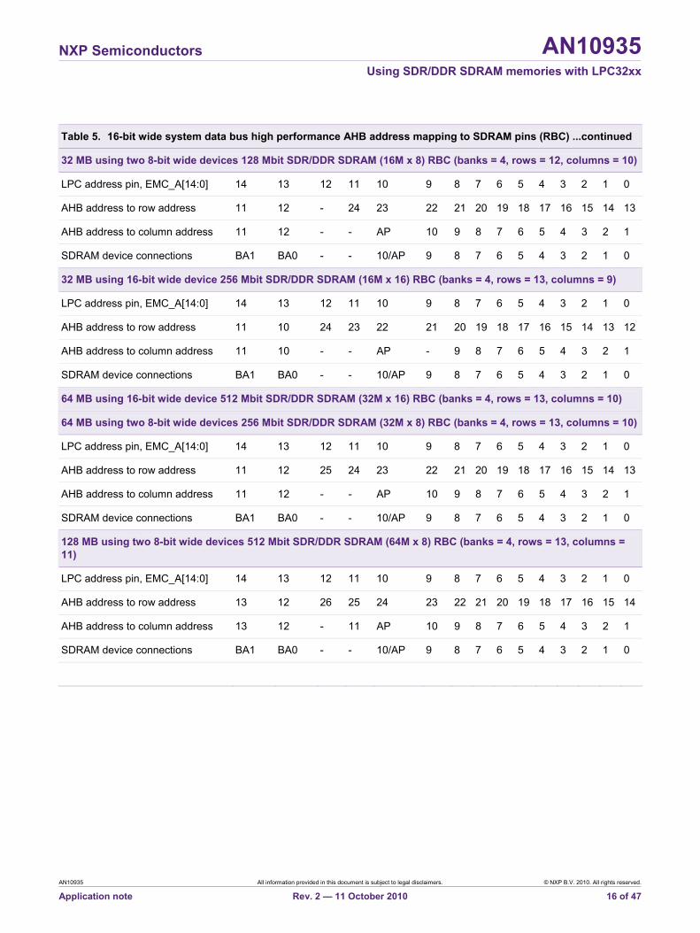
Table 5. 16-bit wide system data bus high performance AHB address mapping to SDRAM pins (RBC) ...continued
32 MB using two 8-bit wide devices 128 Mbit SDR/DDR SDRAM (16M x 8) RBC (banks = 4, rows = 12, columns = 10)
LPC address pin, EMC_A[14:0] 14 13 12 11 10 9 8 7 6 5 4 3 2 1 0
AHB address to row address 11 12 - 24 23 22 21 20 19 18 17 16 15 14 13
AHB address to column address 11 12 - - AP 10 9 8 7 6 5 4 3 2 1
SDRAM device connections BA1 BA0 - - 10/AP 9 8 7 6 5 4 3 2 1 0
32 MB using 16-bit wide device 256 Mbit SDR/DDR SDRAM (16M x 16) RBC (banks = 4, rows = 13, columns = 9)
LPC address pin, EMC_A[14:0] 14 13 12 11 10 9 8 7 6 5 4 3 2 1 0
AHB address to row address 11 10 24 23 22 21 20 19 18 17 16 15 14 13 12
AHB address to column address 11 10 - - AP - 9 8 7 6 5 4 3 2 1
SDRAM device connections BA1 BA0 - - 10/AP 9 8 7 6 5 4 3 2 1 0
64 MB using 16-bit wide device 512 Mbit SDR/DDR SDRAM (32M x 16) RBC (banks = 4, rows = 13, columns = 10)
64 MB using two 8-bit wide devices 256 Mbit SDR/DDR SDRAM (32M x 8) RBC (banks = 4, rows = 13, columns = 10)
LPC address pin, EMC_A[14:0] 14 13 12 11 10 9 8 7 6 5 4 3 2 1 0
AHB address to row address 11 12 25 24 23 22 21 20 19 18 17 16 15 14 13
AHB address to column address 11 12 - - AP 10 9 8 7 6 5 4 3 2 1
SDRAM device connections BA1 BA0 - - 10/AP 9 8 7 6 5 4 3 2 1 0
128 MB using two 8-bit wide devices 512 Mbit SDR/DDR SDRAM (64M x 8) RBC (banks = 4, rows = 13, columns = 11)
LPC address pin, EMC_A[14:0] 14 13 12 11 10 9 8 7 6 5 4 3 2 1 0
AHB address to row address 13 12 26 25 24 23 22 21 20 19 18 17 16 15 14
AHB address to column address 13 12 - 11 AP 10 9 8 7 6 5 4 3 2 1
SDRAM device connections BA1 BA0 - - 10/AP 9 8 7 6 5 4 3 2 1 0
AN10935 All information provided in this document is subject to legal disclaimers. © NXP B.V. 2010. All rights reserved.
Application note Rev. 2 — 11 October 2010 16 of 47
NXP Semiconductors AN10935 Using SDR/DDR SDRAM memories with LPC32xx
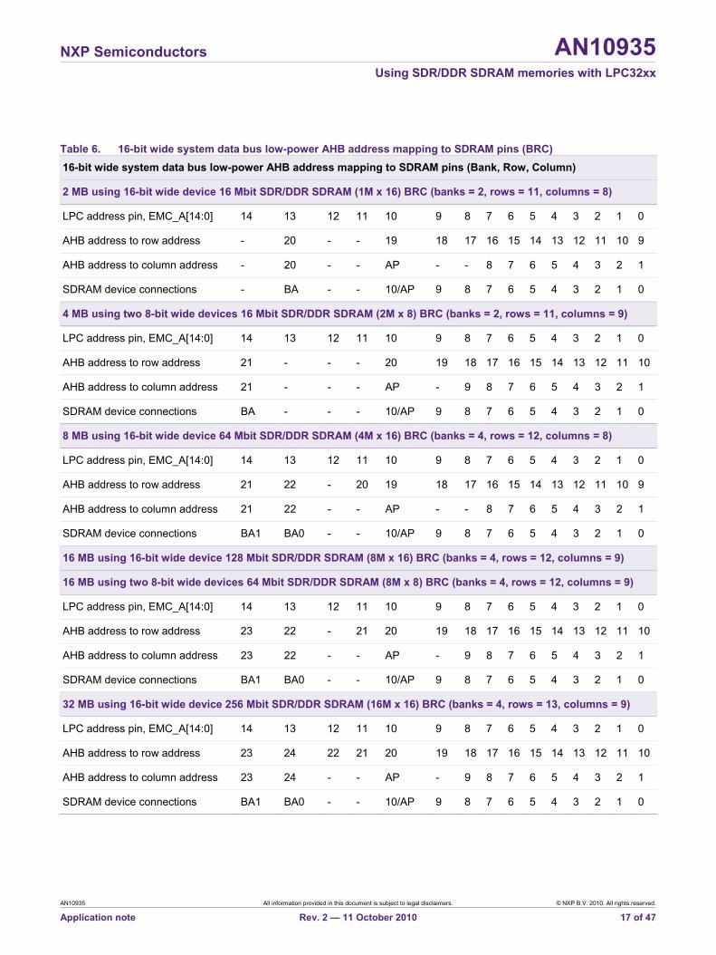
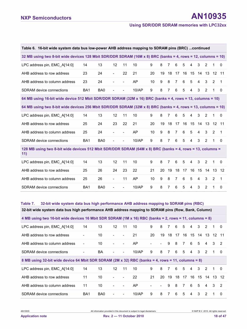
Table 6. 16-bit wide system data bus low-power AHB address mapping to SDRAM pins (BRC) 16-bit wide system data bus low-power AHB address mapping to SDRAM pins (Bank, Row, Column)
2 MB using 16-bit wide device 16 Mbit SDR/DDR SDRAM (1M x 16) BRC (banks = 2, rows = 11, columns = 8)
LPC address pin, EMC_A[14:0] 14 13 12 11 10 9 8 7 6 5 4 3 2 1 0
AHB address to row address - 20 - - 19 18 17 16 15 14 13 12 11 10 9
AHB address to column address - 20 - - AP - - 8 7 6 5 4 3 2 1
SDRAM device connections - BA - - 10/AP 9 8 7 6 5 4 3 2 1 0
4 MB using two 8-bit wide devices 16 Mbit SDR/DDR SDRAM (2M x 8) BRC (banks = 2, rows = 11, columns = 9)
LPC address pin, EMC_A[14:0] 14 13 12 11 10 9 8 7 6 5 4 3 2 1 0
AHB address to row address 21 - - - 20 19 18 17 16 15 14 13 12 11 10
AHB address to column address 21 - - - AP - 9 8 7 6 5 4 3 2 1
SDRAM device connections BA - - - 10/AP 9 8 7 6 5 4 3 2 1 0
8 MB using 16-bit wide device 64 Mbit SDR/DDR SDRAM (4M x 16) BRC (banks = 4, rows = 12, columns = 8)
LPC address pin, EMC_A[14:0] 14 13 12 11 10 9 8 7 6 5 4 3 2 1 0
AHB address to row address 21 22 - 20 19 18 17 16 15 14 13 12 11 10 9
AHB address to column address 21 22 - - AP - - 8 7 6 5 4 3 2 1
SDRAM device connections BA1 BA0 - - 10/AP 9 8 7 6 5 4 3 2 1 0
16 MB using 16-bit wide device 128 Mbit SDR/DDR SDRAM (8M x 16) BRC (banks = 4, rows = 12, columns = 9)
16 MB using two 8-bit wide devices 64 Mbit SDR/DDR SDRAM (8M x 8) BRC (banks = 4, rows = 12, columns = 9)
LPC address pin, EMC_A[14:0] 14 13 12 11 10 9 8 7 6 5 4 3 2 1 0
AHB address to row address 23 22 - 21 20 19 18 17 16 15 14 13 12 11 10
AHB address to column address 23 22 - - AP - 9 8 7 6 5 4 3 2 1
SDRAM device connections BA1 BA0 - - 10/AP 9 8 7 6 5 4 3 2 1 0
32 MB using 16-bit wide device 256 Mbit SDR/DDR SDRAM (16M x 16) BRC (banks = 4, rows = 13, columns = 9)
LPC address pin, EMC_A[14:0] 14 13 12 11 10 9 8 7 6 5 4 3 2 1 0
AHB address to row address 23 24 22 21 20 19 18 17 16 15 14 13 12 11 10
AHB address to column address 23 24 - - AP - 9 8 7 6 5 4 3 2 1
SDRAM device connections BA1 BA0 - - 10/AP 9 8 7 6 5 4 3 2 1 0
AN10935 All information provided in this document is subject to legal disclaimers. © NXP B.V. 2010. All rights reserved.
Application note Rev. 2 — 11 October 2010 17 of 47
NXP Semiconductors AN10935 Using SDR/DDR SDRAM memories with LPC32xx
Table 6. 16-bit wide system data bus low-power AHB address mapping to SDRAM pins (BRC) ...continued
32 MB using two 8-bit wide devices 128 Mbit SDR/DDR SDRAM (16M x 8) BRC (banks = 4, rows = 12, columns = 10)
LPC address pin, EMC_A[14:0] 14 13 12 11 10 9 8 7 6 5 4 3 2 1 0
AHB address to row address 23 24 - 22 21 20 19 18 17 16 15 14 13 12 11
AHB address to column address 23 24 - - AP 10 9 8 7 6 5 4 3 2 1
SDRAM device connections BA1 BA0 - - 10/AP 9 8 7 6 5 4 3 2 1 0
64 MB using 16-bit wide device 512 Mbit SDR/DDR SDRAM (32M x 16) BRC (banks = 4, rows = 13, columns = 10)
64 MB using two 8-bit wide devices 256 Mbit SDR/DDR SDRAM (32M x 8) BRC (banks = 4, rows = 13, columns = 10)
LPC address pin, EMC_A[14:0] 14 13 12 11 10 9 8 7 6 5 4 3 2 1 0
AHB address to row address 25 24 23 22 21 20 19 18 17 16 15 14 13 12 11
AHB address to column address 25 24 - - AP 10 9 8 7 6 5 4 3 2 1
SDRAM device connections BA1 BA0 - - 10/AP 9 8 7 6 5 4 3 2 1 0
128 MB using two 8-bit wide devices 512 Mbit SDR/DDR SDRAM (64M x 8) BRC (banks = 4, rows = 13, columns = 11)
LPC address pin, EMC_A[14:0] 14 13 12 11 10 9 8 7 6 5 4 3 2 1 0
AHB address to row address 25 26 24 23 22 21 20 19 18 17 16 15 14 13 12
AHB address to column address 25 26 - 11 AP 10 9 8 7 6 5 4 3 2 1
SDRAM device connections BA1 BA0 - - 10/AP 9 8 7 6 5 4 3 2 1 0
Table 7. 32-bit wide system data bus high performance AHB address mapping to SDRAM pins (RBC) 32-bit wide system data bus high performance AHB address mapping to SDRAM pins (Row, Bank, Column)
4 MB using two 16-bit wide devices 16 Mbit SDR SDRAM (1M x 16) RBC (banks = 2, rows = 11, columns = 8)
LPC address pin, EMC_A[14:0] 14 13 12 11 10 9 8 7 6 5 4 3 2 1 0
AHB address to row address - 10 - - 21 20 19 18 17 16 15 14 13 12 11
AHB address to column address - 10 - - AP - - 9 8 7 6 5 4 3 2
SDRAM device connections - BA - - 10/AP 9 8 7 6 5 4 3 2 1 0
8 MB using 32-bit wide device 64 Mbit SDR SDRAM (2M x 32) RBC (banks = 4, rows = 11, columns = 8)
LPC address pin, EMC_A[14:0] 14 13 12 11 10 9 8 7 6 5 4 3 2 1 0
AHB address to row address 11 10 - - 22 21 20 19 18 17 16 15 14 13 12
AHB address to column address 11 10 - - AP - - 9 8 7 6 5 4 3 2
SDRAM device connections BA1 BA0 - - 10/AP 9 8 7 6 5 4 3 2 1 0
AN10935 All information provided in this document is subject to legal disclaimers. © NXP B.V. 2010. All rights reserved.
Application note Rev. 2 — 11 October 2010 18 of 47
NXP Semiconductors AN10935 Using SDR/DDR SDRAM memories with LPC32xx
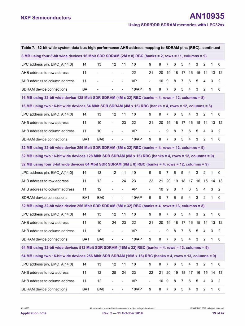
Table 7. 32-bit wide system data bus high performance AHB address mapping to SDRAM pins (RBC)...continued
8 MB using four 8-bit wide devices 16 Mbit SDR SDRAM (2M x 8) RBC (banks = 2, rows = 11, columns = 9)
LPC address pin, EMC_A[14:0] 14 13 12 11 10 9 8 7 6 5 4 3 2 1 0
AHB address to row address 11 - - - 22 21 20 19 18 17 16 15 14 13 12
AHB address to column address 11 - - - AP - 10 9 8 7 6 5 4 3 2
SDRAM device connections BA - - - 10/AP 9 8 7 6 5 4 3 2 1 0
16 MB using 32-bit wide device 128 Mbit SDR SDRAM (4M x 32) RBC (banks = 4, rows = 12, columns = 8)
16 MB using two 16-bit wide devices 64 Mbit SDR SDRAM (4M x 16) RBC (banks = 4, rows = 12, columns = 8)
LPC address pin, EMC_A[14:0] 14 13 12 11 10 9 8 7 6 5 4 3 2 1 0
AHB address to row address 11 10 - 23 22 21 20 19 18 17 16 15 14 13 12
AHB address to column address 11 10 - - AP - - 9 8 7 6 5 4 3 2
SDRAM device connections BA1 BA0 - - 10/AP 9 8 7 6 5 4 3 2 1 0
32 MB using 32-bit wide device 256 Mbit SDR SDRAM (8M x 32) RBC (banks = 4, rows = 12, columns = 9)
32 MB using two 16-bit wide devices 128 Mbit SDR SDRAM (8M x 16) RBC (banks = 4, rows = 12, columns = 9)
32 MB using four 8-bit wide devices 64 Mbit SDR SDRAM (8M x 8) RBC (banks = 4, rows = 12, columns = 9)
LPC address pin, EMC_A[14:0] 14 13 12 11 10 9 8 7 6 5 4 3 2 1 0
AHB address to row address 11 12 - 24 23 22 21 20 19 18 17 16 15 14 13
AHB address to column address 11 12 - - AP - 10 9 8 7 6 5 4 3 2
SDRAM device connections BA1 BA0 - - 10/AP 9 8 7 6 5 4 3 2 1 0
32 MB using 32-bit wide device 256 Mbit SDR SDRAM (8M x 32) RBC (banks = 4, rows = 13, columns = 8)
LPC address pin, EMC_A[14:0] 14 13 12 11 10 9 8 7 6 5 4 3 2 1 0
AHB address to row address 11 10 24 23 22 21 20 19 18 17 16 15 14 13 12
AHB address to column address 11 10 - - AP - - 9 8 7 6 5 4 3 2
SDRAM device connections BA1 BA0 - - 10/AP 9 8 7 6 5 4 3 2 1 0
64 MB using 32-bit wide devices 512 Mbit SDR SDRAM (16M x 32) RBC (banks = 4, rows = 13, columns = 9)
64 MB using two 16-bit wide devices 256 Mbit SDR SDRAM (16M x 16) RBC (banks = 4, rows = 13, columns = 9)
LPC address pin, EMC_A[14:0] 14 13 12 11 10 9 8 7 6 5 4 3 2 1 0
AHB address to row address 11 12 25 24 23 22 21 20 19 18 17 16 15 14 13
AHB address to column address 11 12 - - AP - 10 9 8 7 6 5 4 3 2
SDRAM device connections BA1 BA0 - - 10/AP 9 8 7 6 5 4 3 2 1 0
AN10935 All information provided in this document is subject to legal disclaimers. © NXP B.V. 2010. All rights reserved.
Application note Rev. 2 — 11 October 2010 19 of 47
NXP Semiconductors AN10935 Using SDR/DDR SDRAM memories with LPC32xx
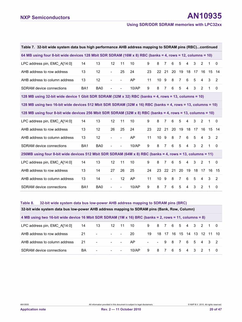
Table 7. 32-bit wide system data bus high performance AHB address mapping to SDRAM pins (RBC)...continued
64 MB using four 8-bit wide devices 128 Mbit SDR SDRAM (16M x 8) RBC (banks = 4, rows = 12, columns = 10)
LPC address pin, EMC_A[14:0] 14 13 12 11 10 9 8 7 6 5 4 3 2 1 0
AHB address to row address 13 12 - 25 24 23 22 21 20 19 18 17 16 15 14
AHB address to column address 13 12 - - AP 11 10 9 8 7 6 5 4 3 2
SDRAM device connections BA1 BA0 - - 10/AP 9 8 7 6 5 4 3 2 1 0
128 MB using 32-bit wide device 1 Gbit SDR SDRAM (32M x 32) RBC (banks = 4, rows = 13, columns = 10)
128 MB using two 16-bit wide devices 512 Mbit SDR SDRAM (32M x 16) RBC (banks = 4, rows = 13, columns = 10)
128 MB using four 8-bit wide devices 256 Mbit SDR SDRAM (32M x 8) RBC (banks = 4, rows = 13, columns = 10)
LPC address pin, EMC_A[14:0] 14 13 12 11 10 9 8 7 6 5 4 3 2 1 0
AHB address to row address 13 12 26 25 24 23 22 21 20 19 18 17 16 15 14
AHB address to column address 13 12 - - AP 11 10 9 8 7 6 5 4 3 2
SDRAM device connections BA1 BA0 - - 10/AP 9 8 7 6 5 4 3 2 1 0
256MB using four 8-bit wide devices 512 Mbit SDR SDRAM (64M x 8) RBC (banks = 4, rows = 13, columns = 11)
LPC address pin, EMC_A[14:0] 14 13 12 11 10 9 8 7 6 5 4 3 2 1 0
AHB address to row address 13 14 27 26 25 24 23 22 21 20 19 18 17 16 15
AHB address to column address 13 14 - 12 AP 11 10 9 8 7 6 5 4 3 2
SDRAM device connections BA1 BA0 - - 10/AP 9 8 7 6 5 4 3 2 1 0
Table 8. 32-bit wide system data bus low-power AHB address mapping to SDRAM pins (BRC) 32-bit wide system data bus low-power AHB address mapping to SDRAM pins (Bank, Row, Column)
4 MB using two 16-bit wide device 16 Mbit SDR SDRAM (1M x 16) BRC (banks = 2, rows = 11, columns = 8)
LPC address pin, EMC_A[14:0] 14 13 12 11 10 9 8 7 6 5 4 3 2 1 0
AHB address to row address 21 - - - 20 19 18 17 16 15 14 13 12 11 10
AHB address to column address 21 - - - AP - - 9 8 7 6 5 4 3 2
SDRAM device connections BA - - - 10/AP 9 8 7 6 5 4 3 2 1 0
AN10935 All information provided in this document is subject to legal disclaimers. © NXP B.V. 2010. All rights reserved.
Application note Rev. 2 — 11 October 2010 20 of 47
NXP Semiconductors AN10935 Using SDR/DDR SDRAM memories with LPC32xx
Table 8. 32-bit wide system data bus low-power AHB address mapping to SDRAM pins (BRC)...continued
8 MB using 32-bit wide device 64 Mbit SDR SDRAM (2M x 32) BRC (banks = 4, rows = 11, columns = 8)
LPC address pin, EMC_A[14:0] 14 13 12 11 10 9 8 7 6 5 4 3 2 1 0
AHB address to row address 21 22 - - 20 19 18 17 16 15 14 13 12 11 10
AHB address to column address 21 22 - - AP - - 9 8 7 6 5 4 3 2
SDRAM device connections BA1 BA0 - - 10/AP 9 8 7 6 5 4 3 2 1 0
8 MB using four 8-bit wide devices 16 Mbit SDR SDRAM (2M x 8) BRC (banks = 2, rows = 11, columns = 9)
LPC address pin, EMC_A[14:0] 14 13 12 11 10 9 8 7 6 5 4 3 2 1 0
AHB address to row address - 22 - - 21 20 19 18 17 16 15 14 13 12 11
AHB address to column address - 22 - - AP - 10 9 8 7 6 5 4 3 2
SDRAM device connections - BA - - 10/AP 9 8 7 6 5 4 3 2 1 0
16 MB using 32-bit wide device 128 Mbit SDR SDRAM (4M x 32) BRC (banks = 4, rows = 12, columns = 8)
16 MB using two 16-bit wide devices 64 Mbit SDR SDRAM (4M x 16) BRC (banks = 4, rows = 12, columns = 8)
LPC address pin, EMC_A[14:0] 14 13 12 11 10 9 8 7 6 5 4 3 2 1 0
AHB address to row address 23 22 - 21 20 19 18 17 16 15 14 13 12 11 10
AHB address to column address 23 22 - - AP - - 9 8 7 6 5 4 3 2
SDRAM device connections BA1 BA0 - - 10/AP 9 8 7 6 5 4 3 2 1 0
32 MB using 32-bit wide device 256 Mbit SDR SDRAM (8M x 32) BRC (banks = 4, rows = 12, columns = 9)
32 MB using two 16-bit wide devices 128 Mbit SDR SDRAM (8M x 16) BRC (banks = 4, rows = 12, columns = 9)
32 MB using four 8-bit wide devices 64 Mbit SDR SDRAM (8M x 8) BRC (banks = 4, rows = 12, columns = 9)
LPC address pin, EMC_A[14:0] 14 13 12 11 10 9 8 7 6 5 4 3 2 1 0
AHB address to row address 23 24 - 22 21 20 19 18 17 16 15 14 13 12 11
AHB address to column address 23 24 - - AP - 10 9 8 7 6 5 4 3 2
SDRAM device connections BA1 BA0 - - 10/AP 9 8 7 6 5 4 3 2 1 0
32 MB using 32-bit wide device 256 Mbit SDR SDRAM (8M x 32) BRC (banks = 4, rows = 13, columns = 8)
LPC address pin, EMC_A[14:0] 14 13 12 11 10 9 8 7 6 5 4 3 2 1 0
AHB address to row address 23 24 22 21 20 19 18 17 16 15 14 13 12 11 10
AHB address to column address 23 24 - - AP - - 9 8 7 6 5 4 3 2
SDRAM device connections BA1 BA0 - - 10/AP 9 8 7 6 5 4 3 2 1 0
AN10935 All information provided in this document is subject to legal disclaimers. © NXP B.V. 2010. All rights reserved.
Application note Rev. 2 — 11 October 2010 21 of 47
NXP Semiconductors AN10935 Using SDR/DDR SDRAM memories with LPC32xx
Table 8. 32-bit wide system data bus low-power AHB address mapping to SDRAM pins (BRC)...continued
64 MB using 32-bit wide device 512 Mbit SDR SDRAM (16M x 32) BRC (banks = 4, rows = 13, columns = 9)
64 MB using two 16-bit wide devices 256 Mbit SDR SDRAM (16M x 16) BRC (banks = 4, rows = 13, columns = 9)
LPC address pin, EMC_A[14:0] 14 13 12 11 10 9 8 7 6 5 4 3 2 1 0
AHB address to row address 25 24 23 22 21 20 19 18 17 16 15 14 13 12 11
AHB address to column address 25 24 - - AP - 10 9 8 7 6 5 4 3 2
SDRAM device connections BA1 BA0 - - 10/AP 9 8 7 6 5 4 3 2 1 0
64 MB using four 8-bit wide devices 128 Mbit SDR SDRAM (16M x 8) BRC (banks = 4, rows = 12, columns = 10)
LPC address pin, EMC_A[14:0] 14 13 12 11 10 9 8 7 6 5 4 3 2 1 0
AHB address to row address 25 24 - 23 22 21 20 19 18 17 16 15 14 13 12
AHB address to column address 25 24 - - AP 11 10 9 8 7 6 5 4 3 2
SDRAM device connections BA1 BA0 - - 10/AP 9 8 7 6 5 4 3 2 1 0
128 MB using 32-bit wide device 1 Gbit SDR SDRAM (32M x 32) BRC (banks = 4, rows = 13, columns = 10)
128 MB using two 16-bit wide devices 512 Mbit SDR SDRAM (32M x 16) BRC (banks = 4, rows = 13, columns = 10)
128 MB using four 8-bit wide devices 256 Mbit SDR SDRAM (32M x 8) BRC (banks = 4, rows = 13, columns = 10)
LPC address pin, EMC_A[14:0] 14 13 12 11 10 9 8 7 6 5 4 3 2 1 0
AHB address to row address 25 26 24 23 22 21 20 19 18 17 16 15 14 13 12
AHB address to column address 25 26 - - AP 11 10 9 8 7 6 5 4 3 2
SDRAM device connections BA1 BA0 - - 10/AP 9 8 7 6 5 4 3 2 1 0
256MB using four 8-bit wide devices 512 Mbit SDR SDRAM (64M x 8) BRC (banks = 4, rows = 13, columns = 11)
LPC address pin, EMC_A[14:0] 14 13 12 11 10 9 8 7 6 5 4 3 2 1 0
AHB address to row address 27 26 25 24 23 22 21 20 19 18 17 16 15 14 13
AHB address to column address 27 26 - 12 AP 11 10 9 8 7 6 5 4 3 2
SDRAM device connections BA1 BA0 - - 10/AP 9 8 7 6 5 4 3 2 1 0
AN10935 All information provided in this document is subject to legal disclaimers. © NXP B.V. 2010. All rights reserved.
Application note Rev. 2 — 11 October 2010 22 of 47
NXP Semiconductors AN10935 Using SDR/DDR SDRAM memories with LPC32xx
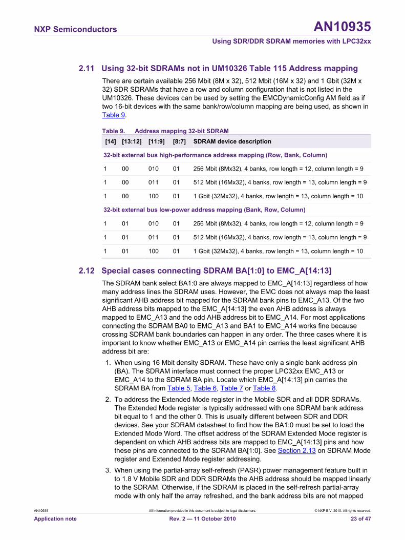
2.11 Using 32-bit SDRAMs not in UM10326 Table 115 Address mapping There are certain available 256 Mbit (8M x 32), 512 Mbit (16M x 32) and 1 Gbit (32M x 32) SDR SDRAMs that have a row and column configuration that is not listed in the UM10326. These devices can be used by setting the EMCDynamicConfig AM field as if two 16-bit devices with the same bank/row/column mapping are being used, as shown in Table 9.
Table 9. Address mapping 32-bit SDRAM [14] [13:12] [11:9] [8:7] SDRAM device description
32-bit external bus high-performance address mapping (Row, Bank, Column)
1 00 010 01 256 Mbit (8Mx32), 4 banks, row length = 12, column length = 9
1 00 011 01 512 Mbit (16Mx32), 4 banks, row length = 13, column length = 9
1 00 100 01 1 Gbit (32Mx32), 4 banks, row length = 13, column length = 10
32-bit external bus low-power address mapping (Bank, Row, Column)
1 01 010 01 256 Mbit (8Mx32), 4 banks, row length = 12, column length = 9
1 01 011 01 512 Mbit (16Mx32), 4 banks, row length = 13, column length = 9
1 01 100 01 1 Gbit (32Mx32), 4 banks, row length = 13, column length = 10
2.12 Special cases connecting SDRAM BA[1:0] to EMC_A[14:13] The SDRAM bank select BA1:0 are always mapped to EMC_A[14:13] regardless of how many address lines the SDRAM uses. However, the EMC does not always map the least significant AHB address bit mapped for the SDRAM bank pins to EMC_A13. Of the two AHB address bits mapped to the EMC_A[14:13] the even AHB address is always mapped to EMC_A13 and the odd AHB address bit to EMC_A14. For most applications connecting the SDRAM BA0 to EMC_A13 and BA1 to EMC_A14 works fine because crossing SDRAM bank boundaries can happen in any order. The three cases where it is important to know whether EMC_A13 or EMC_A14 pin carries the least significant AHB address bit are: 1. When using 16 Mbit density SDRAM. These have only a single bank address pin
(BA). The SDRAM interface must connect the proper LPC32xx EMC_A13 or EMC_A14 to the SDRAM BA pin. Locate which EMC_A[14:13] pin carries the SDRAM BA from Table 5, Table 6, Table 7 or Table 8.
2. To address the Extended Mode register in the Mobile SDR and all DDR SDRAMs. The Extended Mode register is typically addressed with one SDRAM bank address bit equal to 1 and the other 0. This is usually different between SDR and DDR devices. See your SDRAM datasheet to find how the BA1:0 must be set to load the Extended Mode Word. The offset address of the SDRAM Extended Mode register is dependent on which AHB address bits are mapped to EMC_A[14:13] pins and how these pins are connected to the SDRAM BA[1:0]. See Section 2.13 on SDRAM Mode register and Extended Mode register addressing.
3. When using the partial-array self-refresh (PASR) power management feature built in to 1.8 V Mobile SDR and DDR SDRAMs the AHB address should be mapped linearly to the SDRAM. Otherwise, if the SDRAM is placed in the self-refresh partial-array mode with only half the array refreshed, and the bank address bits are not mapped
AN10935 All information provided in this document is subject to legal disclaimers. © NXP B.V. 2010. All rights reserved.
Application note Rev. 2 — 11 October 2010 23 of 47
NXP Semiconductors AN10935 Using SDR/DDR SDRAM memories with LPC32xx
linearly to the AHB address, what the SDRAM refreshes will map to banks 0 and 2 in the LPC32xx address space. To ensure the AHB address is mapped linearly to the SDRAM, the 16/32-bit Low power address mapping must be programmed in to EMCDynamicConfig AM field, and the hardware SDRAM interface must connect the SDRAM BA0 to EMC_A14 or EMC_A13 depending on which carries the least significant AHB address bit. For Low-power AHB address to EMC_A[14:13] mapping see Table 6 or Table 8.
2.13 Loading the SDRAM Mode Register or Extended Mode register The address used to load the SDRAM Mode Register (MR) or Mobile SDR and DDR Extended Mode Register (EMR) is dependent on the SDRAM density, which address mapping is used (RBC or BRC), and how the SDRAM BA[1:0] pins are connected to EMC_A[14:13]. The value you wish to load at either the SDRAM MR or EMR register must be shifted left the proper number of bits to occupy the Row address bit positions (EMC_A(12:0) pins) in the AHB address to Row address mapping found in Table 5, Table 6, Table 7 or Table 8.
The SDRAM BA[1:0] value will determine whether the Mode register (BA[1:0] = 0b00) or Extended Mode register (BA[1:0] = 0b10 or 0b01) is loaded. See the Mobile/Low Power SDRAM datasheet to confirm the BA1:0 value to load the Extended Mode Word.
The address for the mode word operation is as follows:
Chip select 0: address = 0x80000000 + (mode_word << (offset))
Chip select 1: address = 0xA0000000 + (mode_word << (offset))
The <offset> value can be determined with the following formulas:
BRC mapping/16-bit device: (offset) = (column bits) + 1
RBC mapping/16-bit device: (offset) = (column bits + bank bits ) + 1
BRC mapping/32-bit device: (offset) = (column bits) + 2
RBC mapping/32-bit device: (offset) = (column bits + bank bits ) + 2
Example: For a 16-bit device with 9 columns and 4 banks (2 bits of bank address) in RBC mapping on chip select 0 writing the mode word 0x21, the physical mode word address is (0x80000000 + (0x21 << (9 +2 + 1) = 0x80021000.
AN10935 All information provided in this document is subject to legal disclaimers. © NXP B.V. 2010. All rights reserved.
Application note Rev. 2 — 11 October 2010 24 of 47
NXP Semiconductors AN10935 Using SDR/DDR SDRAM memories with LPC32xx
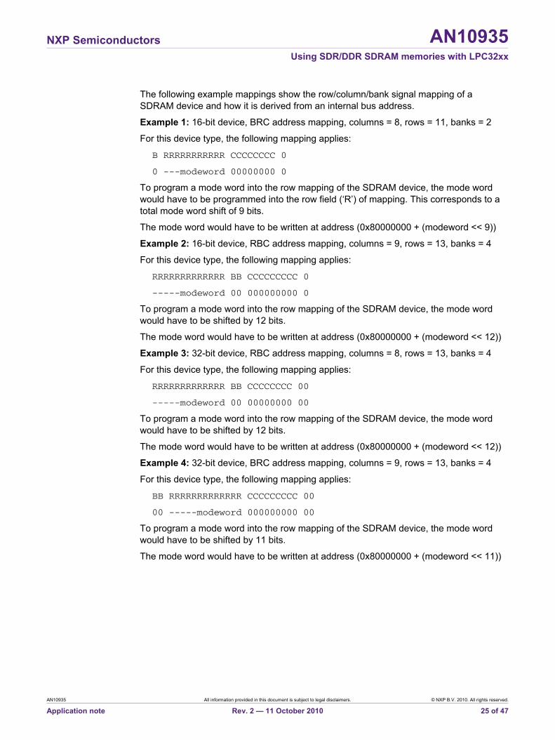
The following example mappings show the row/column/bank signal mapping of a SDRAM device and how it is derived from an internal bus address.
Example 1: 16-bit device, BRC address mapping, columns = 8, rows = 11, banks = 2
For this device type, the following mapping applies:
B RRRRRRRRRRR CCCCCCCC 0
0 ---modeword 00000000 0
To program a mode word into the row mapping of the SDRAM device, the mode word would have to be programmed into the row field (‘R’) of mapping. This corresponds to a total mode word shift of 9 bits.
The mode word would have to be written at address (0x80000000 + (modeword << 9))
Example 2: 16-bit device, RBC address mapping, columns = 9, rows = 13, banks = 4
For this device type, the following mapping applies:
RRRRRRRRRRRRR BB CCCCCCCCC 0
-----modeword 00 000000000 0
To program a mode word into the row mapping of the SDRAM device, the mode word would have to be shifted by 12 bits.
The mode word would have to be written at address (0x80000000 + (modeword << 12))
Example 3: 32-bit device, RBC address mapping, columns = 8, rows = 13, banks = 4
For this device type, the following mapping applies:
RRRRRRRRRRRRR BB CCCCCCCC 00
-----modeword 00 00000000 00
To program a mode word into the row mapping of the SDRAM device, the mode word would have to be shifted by 12 bits.
The mode word would have to be written at address (0x80000000 + (modeword << 12))
Example 4: 32-bit device, BRC address mapping, columns = 9, rows = 13, banks = 4
For this device type, the following mapping applies:
BB RRRRRRRRRRRRR CCCCCCCCC 00
00 -----modeword 000000000 00
To program a mode word into the row mapping of the SDRAM device, the mode word would have to be shifted by 11 bits.
The mode word would have to be written at address (0x80000000 + (modeword << 11))
AN10935 All information provided in this document is subject to legal disclaimers. © NXP B.V. 2010. All rights reserved.
Application note Rev. 2 — 11 October 2010 25 of 47
NXP Semiconductors AN10935 Using SDR/DDR SDRAM memories with LPC32xx
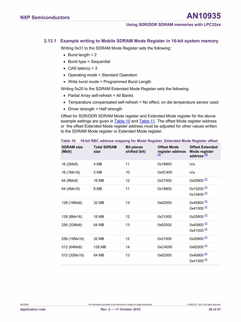
2.13.1 Example writing to Mobile SDRAM Mode Register in 16-bit system memory Writing 0x31 to the SDRAM Mode Register sets the following:
• Burst length = 2 • Burst type = Sequential • CAS latency = 3 • Operating mode = Standard Operation • Write burst mode = Programmed Burst Length
Writing 0x20 to the SDRAM Extended Mode Register sets the following: • Partial Array self-refresh = All Banks • Temperature compensated self-refresh = No effect, on die temperature sensor used • Driver strength = Half strength
Offset for SDR/DDR SDRAM Mode register and Extended Mode register for the above example settings are given in Table 10 and Table 11. The offset Mode register address or the offset Extended Mode register address must be adjusted for other values written to the SDRAM Mode register or Extended Mode register.
Table 10. 16-bit RBC address mapping for Mode Register, Extended Mode Register offset SDRAM size (Mbit)
Total SDRAM size
Bit places shifted (bit)
Offset Mode register address [1]
Offset Extended Mode register address [1]
16 (2Mx8) 4 MB 11 0x18800 n/a
16 (1Mx16) 2 MB 10 0x0C400 n/a
64 (8Mx8) 16 MB 12 0x31000 0x20800 [2]
64 (4Mx16) 8 MB 11 0x18800 0x10200 [2] 0x10400 [3]
128 (16Mx8) 32 MB 13 0x62000 0x40800 [2] 0x41000 [3]
128 (8Mx16) 16 MB 12 0x31000 0x20800 [2]
256 (32Mx8) 64 MB 13 0x62000 0x40800 [2] 0x41000 [3]
256 (16Mx16) 32 MB 12 0x31000 0x20800 [2]
512 (64Mx8) 128 MB 14 0xC4000 0x82000 [2]
512 (32Mx16) 64 MB 13 0x62000 0x40800 [2] 0x41000 [3]
AN10935 All information provided in this document is subject to legal disclaimers. © NXP B.V. 2010. All rights reserved.
Application note Rev. 2 — 11 October 2010 26 of 47
NXP Semiconductors AN10935 Using SDR/DDR SDRAM memories with LPC32xx
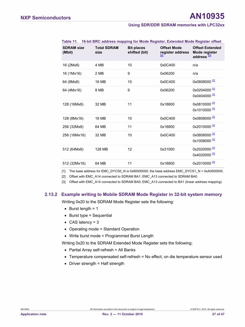
Table 11. 16-bit BRC address mapping for Mode Register, Extended Mode Register offset SDRAM size (Mbit)
Total SDRAM size
Bit places shifted (bit)
Offset Mode register address [1]
Offset Extended Mode register address [1]
16 (2Mx8) 4 MB 10 0x0C400 n/a
16 (1Mx16) 2 MB 9 0x06200 n/a
64 (8Mx8) 16 MB 10 0x0C400 0x0808000 [2]
64 (4Mx16) 8 MB 9 0x06200 0x0204000 [2] 0x0404000 [3]
128 (16Mx8) 32 MB 11 0x18800 0x0810000 [2] 0x1010000 [3]
128 (8Mx16) 16 MB 10 0x0C400 0x0808000 [2]
256 (32Mx8) 64 MB 11 0x18800 0x2010000 [2]
256 (16Mx16) 32 MB 10 0x0C400 0x0808000 [2] 0x1008000 [3]
512 (64Mx8) 128 MB 12 0x31000 0x2020000 [2] 0x4020000 [3]
512 (32Mx16) 64 MB 11 0x18800 0x2010000 [2]
[1] The base address for EMC_DYCS0_N is 0x80000000; the base address EMC_DYCS1_N = 0xA0000000. [2] Offset with EMC_A14 connected to SDRAM BA1; EMC_A13 connected to SDRAM BA0. [3] Offset with EMC_A14 connected to SDRAM BA0; EMC_A13 connected to BA1 (linear address mapping).
2.13.2 Example writing to Mobile SDRAM Mode Register in 32-bit system memory Writing 0x20 to the SDRAM Mode Register sets the following:
• Burst length = 1 • Burst type = Sequential • CAS latency = 3 • Operating mode = Standard Operation • Write burst mode = Programmed Burst Length
Writing 0x20 to the SDRAM Extended Mode Register sets the following: • Partial Array self-refresh = All Banks • Temperature compensated self-refresh = No effect, on die temperature sensor used • Driver strength = Half strength
AN10935 All information provided in this document is subject to legal disclaimers. © NXP B.V. 2010. All rights reserved.
Application note Rev. 2 — 11 October 2010 27 of 47
NXP Semiconductors AN10935 Using SDR/DDR SDRAM memories with LPC32xx
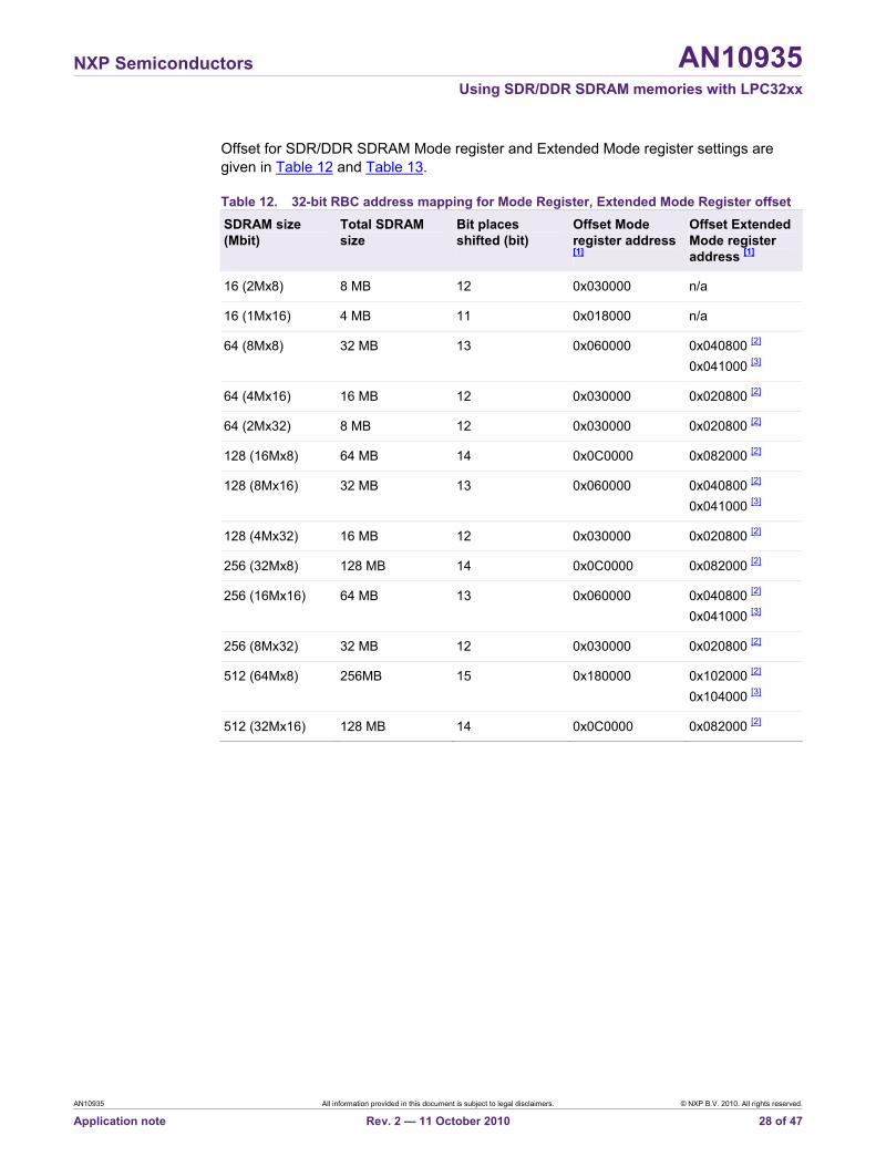
Offset for SDR/DDR SDRAM Mode register and Extended Mode register settings are given in Table 12 and Table 13.
Table 12. 32-bit RBC address mapping for Mode Register, Extended Mode Register offset SDRAM size (Mbit)
Total SDRAM size
Bit places shifted (bit)
Offset Mode register address [1]
Offset Extended Mode register address [1]
16 (2Mx8) 8 MB 12 0x030000 n/a
16 (1Mx16) 4 MB 11 0x018000 n/a
64 (8Mx8) 32 MB 13 0x060000 0x040800 [2] 0x041000 [3]
64 (4Mx16) 16 MB 12 0x030000 0x020800 [2]
64 (2Mx32) 8 MB 12 0x030000 0x020800 [2]
128 (16Mx8) 64 MB 14 0x0C0000 0x082000 [2]
128 (8Mx16) 32 MB 13 0x060000 0x040800 [2] 0x041000 [3]
128 (4Mx32) 16 MB 12 0x030000 0x020800 [2]
256 (32Mx8) 128 MB 14 0x0C0000 0x082000 [2]
256 (16Mx16) 64 MB 13 0x060000 0x040800 [2] 0x041000 [3]
256 (8Mx32) 32 MB 12 0x030000 0x020800 [2]
512 (64Mx8) 256MB 15 0x180000 0x102000 [2] 0x104000 [3]
512 (32Mx16) 128 MB 14 0x0C0000 0x082000 [2]
AN10935 All information provided in this document is subject to legal disclaimers. © NXP B.V. 2010. All rights reserved.
Application note Rev. 2 — 11 October 2010 28 of 47
NXP Semiconductors AN10935 Using SDR/DDR SDRAM memories with LPC32xx
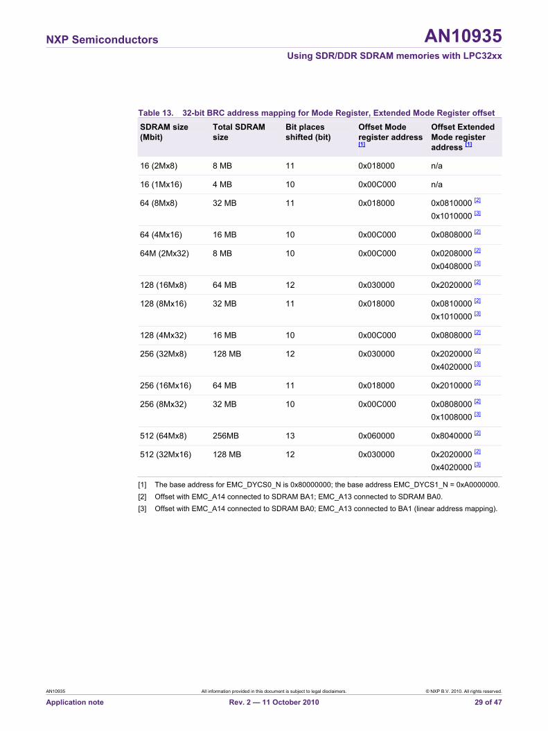
Table 13. 32-bit BRC address mapping for Mode Register, Extended Mode Register offset SDRAM size (Mbit)
Total SDRAM size
Bit places shifted (bit)
Offset Mode register address [1]
Offset Extended Mode register address [1]
16 (2Mx8) 8 MB 11 0x018000 n/a
16 (1Mx16) 4 MB 10 0x00C000 n/a
64 (8Mx8) 32 MB 11 0x018000 0x0810000 [2] 0x1010000 [3]
64 (4Mx16) 16 MB 10 0x00C000 0x0808000 [2]
64M (2Mx32) 8 MB 10 0x00C000 0x0208000 [2] 0x0408000 [3]
128 (16Mx8) 64 MB 12 0x030000 0x2020000 [2]
128 (8Mx16) 32 MB 11 0x018000 0x0810000 [2] 0x1010000 [3]
128 (4Mx32) 16 MB 10 0x00C000 0x0808000 [2]
256 (32Mx8) 128 MB 12 0x030000 0x2020000 [2] 0x4020000 [3]
256 (16Mx16) 64 MB 11 0x018000 0x2010000 [2]
256 (8Mx32) 32 MB 10 0x00C000 0x0808000 [2] 0x1008000 [3]
512 (64Mx8) 256MB 13 0x060000 0x8040000 [2]
512 (32Mx16) 128 MB 12 0x030000 0x2020000 [2] 0x4020000 [3]
[1] The base address for EMC_DYCS0_N is 0x80000000; the base address EMC_DYCS1_N = 0xA0000000. [2] Offset with EMC_A14 connected to SDRAM BA1; EMC_A13 connected to SDRAM BA0. [3] Offset with EMC_A14 connected to SDRAM BA0; EMC_A13 connected to BA1 (linear address mapping).
AN10935 All information provided in this document is subject to legal disclaimers. © NXP B.V. 2010. All rights reserved.
Application note Rev. 2 — 11 October 2010 29 of 47
NXP Semiconductors AN10935 Using SDR/DDR SDRAM memories with LPC32xx
3. SDRAM controller programming and operations SDRAM devices are more complex to setup than standard asynchronous memories. In addition to setting up the interface signal timings – factors such as RAS and CAS latency (also referred to as RAS and CAS delay), burst size, and refresh timing need to be considered. For DDR based memories that run at high clock frequencies, the correct setup of the self calibration features in the LPC32x0 also become important for normal operation.
SDRAM setup is procedural and requires a series of steps to initialize and configure SDRAM.
3.1 Typical SDRAM programming sequences To program the SDRAM controller for a specific SDRAM device, the following information about the system using the SDRAM devices is needed:
• Desired clock speed for the SDRAM access speed − In SDR based systems, this can be up to the CPU clock rate, ½ the CPU clock
rate, or ¼ the CPU clock rate − In DDR systems, the DDR clock can only run at ½ or ¼ the CPU clock speed.
• SDRAM types (voltage) − Low power (mobile) or standard DRAMS, SDR or DDR SDRAM
• SDRAM geometry − Number of columns, rows, and banks of the device
• Expected RAS and CAS cycles (may be limited by memory speed and board design) • SDRAM access (or address) strategy: low-power or high-performance mode • SDRAM data bus width • SDRAM interface timings (from the SDRAM datasheet) • Dynamic refresh period timing
SDR and DDR SDRAM types are slightly different in their programming sequence. These programming sequences are meant as guidelines only.
3.1.1 Standard and low power SDR SDRAM programming sequence Following are the typical steps necessary to program the SDRAM controller and a SDR SDRAM type device. Prior to these steps, it is assumed the main system clocking has already been setup and the system is running at the desired clock rate. For this type of SDRAM, the bus clock (HCLK) used to drive the SDRAM can run at up to 133 MHz at a ratio of 1, ½, or ¼ the CPU speed.
Note the programming sequence defined below is based on the JDEC programming sequence and includes the proper steps to setup the SDRAM and the controller. Low power and standard SDR SDRAM programming sequences are similar, with the exception of an extra extended mode register programming cycle on low power devices.
Step 1: Enable EMC clocking, select SDRAM type, and select SDRAM slew rates
Before any accesses to the EMC can occur, the EMC clock needs to be enabled. The EMC clock can be enabled by clearing bit 0 in the Clock and Power SDRAM Clock Control Register. SDR SDRAM must also be selected in this register by clearing bit 1. Slew rates can also be set to fast or slow in this register with bits 22..20.
AN10935 All information provided in this document is subject to legal disclaimers. © NXP B.V. 2010. All rights reserved.
Application note Rev. 2 — 11 October 2010 30 of 47
NXP Semiconductors AN10935 Using SDR/DDR SDRAM memories with LPC32xx
Step 2: Enable the EMC interface and set EMC endian-ness
The EMC interface can be enabled by setting bit 0 of the EMC Control register. The endian mode can be selected by the EMC Configuration register. In most cases, little endian mode should be used.
Step 3: Set a long period for the dynamic refresh rate
Setting a long period for the dynamic refresh rate prevents the EMC from constantly being in the busy status. Set the EMC Dynamic Memory Refresh Timer register to 0x7FF for the maximum period.
Step 4: Set the HCLK command delay to 7 and select SDR memory
Program a hard-coded value of 7 for the Command delay field (bits 18..14) in the SDRAM Clock Control register. SDR memory is selected by clearing bit 1.
Step 5: Setup address mapping
Setup the row/column/bank address mapping and DRAM type used by the interface. This can be selected with configuring the EMC Dynamic Memory Configuration 0 register. For SDR SDRAM, always use the low power SDR SDRAM value for the Memory device (MD) field (bits 2..0) of this register, regardless of whether standard or low power SDRAM is used in the system.
For the Address Mapping (AM) field (bits 14..7), select a device that matches the SDRAM data bus width (16 or 32-bits) and has the same row/column/bank numbers as the SDRAM device(s). Note the listed size for a mapping isn’t important, only the row/column/bank mapping must match for the selected data bus width. Multiple configurations may exist with the same mapping, but different listed sizes. Either mapping will work. If a device also exists on the 2nd SDRAM chip select, it also needs address mapping to be setup in the EMC Dynamic Memory Configuration 1 register.
Step 6: Setup RAS and CAS latencies
Setup the RAS and CAS latencies in the EMC Dynamic Memory RAS and CAS Delay 0 register. Note the CAS latency supports ½ clock latencies. For SDR SDRAM devices, the CAS latency must be setup in full clock cycles and bit 7 in the CAS latency field must always be 0. If a device also exists on the 2nd SDRAM chip select, it also needs CAS and RAS latency to be setup in the EMC Dynamic Memory RAS and CAS Delay 1 register.
Step 7: Setup the SDRAM command and read strategy
This can be setup in the EMC Dynamic Memory Read Configuration register. For the SDR_SRP and SDR_SRD fields, the positive capture edge and “command delayed by COMMAND_DELAY time” must be used, respectively.
AN10935 All information provided in this document is subject to legal disclaimers. © NXP B.V. 2010. All rights reserved.
Application note Rev. 2 — 11 October 2010 31 of 47
NXP Semiconductors AN10935 Using SDR/DDR SDRAM memories with LPC32xx
Step 8: Setup interface timing
Setup the interface timing parameters for the SDRAM device in the EMC Dynamic Memory timing registers. These registers control the number of bus clocks cycles a specific timing value is delayed. The value for these registers van be obtained from the User’s Guide or datasheet for the SDRAM device. A list of the registers that need to be setup is shown below:
• Precharge Command Period register • Active to Precharge Command Period register • Self-refresh Exit Time register • Write recover Time register • Active to Active Command Period register • Exit Self-refresh to Active Command register • Active Bank A to Active Bank B register • Load Mode register to Active Command Time • Last Data In to Read Command Time register
Values in these registers are based on the bus (HCLK) period. See the LCP3250 User’s Guide for more information on these registers.
Step 9: Enable SDRAM clocks and clock enables and issues NOPs for 100 us
Setup the clock enables (bit 0) and clocks (bit 1) to be always active while issuing the NOP command (bits 8..7) for 100 us. It is recommended to also disabled the inverted memory clock (bit 4) used for DDR mode. These are setup in the EMC Dynamic Memory Control register.
Step 10: Issue precharge-all command
Setup the clock enables (bit 0) and clocks (bit 1) to be always active while issuing the Precharge-all command (bits 8..7) for 10 us. Note the dynamic refresh must be set to a fast rate during this command so at least a few dynamic refresh cycles occur during the 10 us period.
Step 11: Set normal dynamic refresh timing
Set the EMC Dynamic Memory Refresh Timer register to the correct value for the optimal refresh period.
Step 12: Issue mode word
Setup the clock enables (bit 0) and clocks (bit 1) to be always active while issuing the mode command (bits 8..7) in the EMC Dynamic Memory Control register. Issue the mode word to the device by writing a value at the mode word address as specified in Section 2.13.1 or Section 2.13.2. The value written to the address isn’t important. After the write, provide a small delay (about 1 us) before performing any SDRAM operations.
The mode word is used to specify the burst length and CAS latency. For 32-bit interfaces, the burst length is always 1. For 16-bit interfaces, the burst length is always 2. The CAS latency must match the latency programmed into the EMC Dynamic Memory RAS and CAS Delay 0 registers.
If a device also exists on the 2nd SDRAM chip select, it also needs mode word configuration.
AN10935 All information provided in this document is subject to legal disclaimers. © NXP B.V. 2010. All rights reserved.
Application note Rev. 2 — 11 October 2010 32 of 47
NXP Semiconductors AN10935 Using SDR/DDR SDRAM memories with LPC32xx
Step 13: Issue extended mode word (low power SDRAM only)
This step applies to low power SDRAM devices only. Standard SDR devices can skip this step.
Setup the clock enables (bit 0) and clocks (bit 1) to be always active while issuing the mode command (bits 8..7) in the EMC Dynamic Memory Control register. Issue the extended mode word to the device by writing a value at the extended mode word address as specified in Section 2.13.1 or Section 2.13.2. The value written to the address isn’t important. After the write, provide a small delay (about 1 us) before performing any SDRAM operations.
The extended mode word is usually used to specify SDRAM drive strength.
If a device also exists on the 2nd SDRAM chip select, it also needs extended mode word configuration.
Step 14: Enter normal operational mode
Setup the clock enables (bit 0) and clocks (bit 1) to be de-asserted when the SDRAM is idle while issuing the normal command (bits 8..7) in the EMC Dynamic Memory Control register. It is recommended that the Inverted memory clock (bit 4) also be disabled for SDR SDRAM. Set the Self Refresh Clock Control (bit 3) in the register so self-refresh mode will automatically disable the SDRAM clock when entered.
At this point, SDRAM should be fully operational.
3.1.2 DDR SDRAM programming sequence Following are the typical steps necessary to program the SDRAM controller and a DDR SDRAM type device. Prior to these steps, it is assumed the main system clocking has already been setup and the system is running at the desired clock rate. For this type of SDRAM, the bus clock (HCLK) used to derive the SDRAM can run at up to 133 MHz at a ratio of ½ or ¼ the CPU speed.
Note the programming sequence defined below is based on the JDEC programming sequence and includes the proper steps to setup the SDRAM and the controller. Low power and standard DDR SDRAM programming sequences are slightly different and have differing steps.
Step 1: Enable EMC clocking, select SDRAM type, and select SDRAM slew rates
Before any accesses to the EMC can occur, the EMC clock needs to be enabled. The EMC clock can be enabled by clearing bit 0 in the Clock and Power SDRAM Clock Control Register. DDR SDRAM must also be selected in this register by setting bit 1. Slew rates can also be set to fast or slow in this register with bits 22..20.
Step 2: Enable the EMC interface and set EMC endian-ness
The EMC interface can be enabled by setting bit 0 of the EMC Control register. The endian mode can be selected by the EMC Configuration register. In most cases, little endian mode should be used.
Step 3: Set a long period for the dynamic refresh rate
Setting a long period for the dynamic refresh rate prevents the EMC from constantly being in the busy status. Set the EMC Dynamic Memory Refresh Timer register to 0x7FF for the maximum period.
AN10935 All information provided in this document is subject to legal disclaimers. © NXP B.V. 2010. All rights reserved.
Application note Rev. 2 — 11 October 2010 33 of 47
NXP Semiconductors AN10935 Using SDR/DDR SDRAM memories with LPC32xx
Step 4: Set the HCLK command delay to 15 and select SDR memory
Program a hard-coded value of 15 for the Command delay field (bits 18..14) in the SDRAM Clock Control register. DDR memory is selected by setting bit 1.
Step 5: Set the external data bus width to 16 bits (optional)
Although this is optional, it is recommended. When the DDR interface is used, several data bits in the upper half of the 32-bit data bus become non-functional.
Step 6: Resynchronize DDR clocking
The DDR clocks need to be resynchronized when clocks are stopped or started, or clock rates change. Failure to do this may result in the SDRAM data becoming misaligned or swapped.
To resynchronize the DDR clocks, first disable the DDR clocking in the HCLK Divider Control register. Then toggle the DDR clock reset bit (bit 19) high and then low again in the SDRAM Clock Control Register. Then restore the DDR clocking in the HCLK Divider Control register to either nominal or ½ speed.
Step 7: Setup address mapping
Setup the row/column/bank address mapping and DRAM type used by the interface. This can be selected with configuring the EMC Dynamic Memory Configuration 0 register. For DDR SDRAM, always use the low power DDR SDRAM value for the Memory device (MD) field (bits 2..0) of this register, regardless of whether standard or low power SDRAM is used in the system.
For the Address Mapping (AM) field (bits 14..7), select a device that matches the SDRAM data bus width (1-bits only) and has the same row/column/bank numbers as the SDRAM device(s). Note the listed size for a mapping isn’t important, only the row/column/bank mapping must match for the selected data bus width. Multiple configurations may exist with the same mapping, but different listed sizes. Either mapping will work. If a device also exists on the 2nd SDRAM chip select, it also needs address mapping to be setup in the EMC Dynamic Memory Configuration 1 register.
Step 8: Determine nominal ring oscillator count for the current operating conditions
For the current systems conditions (Voltage, process, and temperate), force a few calibration runs on the ring oscillator count and save the average value into the nominal ring oscillator count. The nominal value is used as a reference against the dynamic count and is used to slightly alter DDR timing as voltage and temperature change.
To force a calibration cycle, set and clear the SW_DDR_CAL bit in the SDRAM Clock Control register. After clearing the bit, wait at least 1 us and then read the EMC DDR Calibration Delay Value register. This should be averaged over a number of samples and the average value saved in the DDR Calibration Nominal Value register.
Step 9: Setup RAS and CAS latencies
Setup the RAS and CAS latencies in the EMC Dynamic Memory RAS and CAS Delay 0 register. Note the CAS latency supports ½ clock latencies. For low power DDR SDRAM devices, the CAS latency must be setup in full clock cycles and bit 7 in the CAS latency field must always be 0. For standard DDR SDRAM devices, CAS latencies in ½ clock values are allowed. If a device also exists on the 2nd SDRAM chip select, it also needs CAS and RAS latency to be setup in the EMC Dynamic Memory RAS and CAS Delay 1 register.
AN10935 All information provided in this document is subject to legal disclaimers. © NXP B.V. 2010. All rights reserved.
Application note Rev. 2 — 11 October 2010 34 of 47
NXP Semiconductors AN10935 Using SDR/DDR SDRAM memories with LPC32xx
Step 10: Setup the SDRAM command and read strategy
This can be setup ion the EMC Dynamic Memory Read Configuration register. For the DDR_DRD field, the “command delayed by COMMAND_DELAY time” must be used.
For low power DDR systems, the DDR_DRP field should be setup for read data negative capture polarity. For standard power DDR systems, the DDR_DRP field should be setup for read data positive capture polarity.
Step 11: Setup interface timing
Setup the interface timing parameters for the SDRAM device in the EMC Dynamic Memory timing registers. These registers control the number of bus clocks cycles a specific timing value is delayed. The value for these registers van be obtained from the User’s Guide or datasheet for the SDRAM device. A list of the registers that need to be setup is shown below:
• Precharge Command Period register • Active to Precharge Command Period register • Self-refresh Exit Time register • Write recover Time register • Active to Active Command Period register • Exit Self-refresh to Active Command register • Active Bank A to Active Bank B register • Load Mode register to Active Command Time • Last Data In to Read Command Time register
Values in these registers are based on the bus (HCLK) period. See the LCP3250 User’s Guide for more information on these registers.
Step 12: Enable SDRAM clocks and clock enables and issues NOPs for 200 us
Setup the clock enables (bit 0) and clocks (bit 1) to be always active while issuing the NOP command (bits 8..7) for 200 us. These are setup in the EMC Dynamic Memory Control register.
Step 13: Issue precharge-all command
Setup the clock enables (bit 0) and clocks (bit 1) to be always active while issuing the Precharge-all command (bits 8..7) for 10 us. Note the dynamic refresh must be set to a fast rate during this command so at least a few dynamic refresh cycles occur during the 10 us period.
Step 14: Issue extended mode word (standard DDR only)
This step applies to standard DDR devices only and is used to enable the DLL.
Setup the clock enables (bit 0) and clocks (bit 1) to be always active while issuing the mode command (bits 8..7) in the EMC Dynamic Memory Control register. Issue the extended mode word to the device by writing a value at the extended mode word address as specified in Section 2.13.1 or Section 2.13.2. The value written to the address isn’t important. After the write, provide a small delay (about 1 us) before performing any SDRAM operations.
The extended mode word is usually used to specify SDRAM drive strength and enable the SDRAM DLL.
AN10935 All information provided in this document is subject to legal disclaimers. © NXP B.V. 2010. All rights reserved.
Application note Rev. 2 — 11 October 2010 35 of 47
NXP Semiconductors AN10935 Using SDR/DDR SDRAM memories with LPC32xx
If a device also exists on the 2nd SDRAM chip select, it also needs extended mode word configuration.
Step 15: Set normal dynamic refresh timing (low power DDR only)
This step applies to low power DDR devices only.
Set the EMC Dynamic Memory Refresh Timer register to the correct value for the optimal refresh period.
Step 16: Issue mode word
Setup the clock enables (bit 0) and clocks (bit 1) to be always active while issuing the mode command (bits 8..7) in the EMC Dynamic Memory Control register. Issue the mode word to the device by writing a value at the mode word address as specified in Section 2.13.1 or Section 2.13.2. The value written to the address isn’t important. After the write, provide a small delay (about 1 us) before performing any SDRAM operations.
The mode word is used to specify the burst length and CAS latency. For 16-bit interfaces, the burst length is always 2. The CAS latency must match the latency programmed into the EMC Dynamic Memory RAS and CAS Delay 0 registers.
If a device also exists on the 2nd SDRAM chip select, it also needs mode word configuration.
Note: Standard DDR systems issue the mode word with the SDRAM DLL reset command. This doesn’t apply to low power DDR systems.
Step 17: Issue extended mode word (low power DDR only)
This step applies to low power DDR devices only.
Setup the clock enables (bit 0) and clocks (bit 1) to be always active while issuing the mode command (bits 8..7) in the EMC Dynamic Memory Control register. Issue the extended mode word to the device by writing a value at the extended mode word address as specified in Section 2.13.1 or Section 2.13.2. The value written to the address isn’t important. After the write, provide a small delay (about 1 us) before performing any SDRAM operations.
The extended mode word is usually used to specify SDRAM drive strength.
If a device also exists on the 2nd SDRAM chip select, it also needs extended mode word configuration.
Step 18: Issue precharge-all command (standard DDR only)
Setup the clock enables (bit 0) and clocks (bit 1) to be always active while issuing the Precharge-all command (bits 8..7) for 10 us. Note the dynamic refresh must be set to a fast rate during this command so at least a few dynamic refresh cycles occur during the 10 us period.
Step 19: Set normal dynamic refresh timing (standard DDR only)
This step applies to standard DDR devices only.
Set the EMC Dynamic Memory Refresh Timer register to the correct value for the optimal refresh period.
Step 20: Re-issue mode word with DLL reset clear (standard DDR only)
Setup the clock enables (bit 0) and clocks (bit 1) to be always active while issuing the mode command (bits 8..7) in the EMC Dynamic Memory Control register. Issue the mode word to the device by writing a value at the mode word address as specified in
AN10935 All information provided in this document is subject to legal disclaimers. © NXP B.V. 2010. All rights reserved.
Application note Rev. 2 — 11 October 2010 36 of 47
NXP Semiconductors AN10935 Using SDR/DDR SDRAM memories with LPC32xx
Section 2.13.1 or Section 2.13.2. The value written to the address isn’t important. After the write, provide a small delay (about 1 us) before performing any SDRAM operations.
This operation is a repeat of step 16 except with the SDRAM DLL reset clear.
If a device also exists on the 2nd SDRAM chip select, it also needs mode word configuration.
Step 21: Enter normal operational mode
Setup the clock enables (bit 0) and clocks (bit 1) to be de-asserted when the SDRAM is idle while issuing the normal command (bits 8..7) in the EMC Dynamic Memory Control register. Set the Self Refresh Clock Control (bit 3) in the register so self-refresh mode will automatically disable the SDRAM clock when entered.
At this point, SDRAM should be fully operational, although calibration hasn’t yet been enabled.
Step 21: Setup DDR calibration
DDR calibration is explained in Section 3.2.2.
3.1.3 SDR and DDR SDRAM setup example code NXP provides a Common Driver Library (CDL) that contains comprehensive startup and SDRAM initialization code for bringing up new boards. It is highly recommended to use the SDRAM initialization code included with the LPC32x0 Common Driver Library (CDL) to initialize SDRAM and the SDRAM controller.
In addition to the startup and SDRAM initialization code, the CDL provides an application called the Stage 1 Loader (S1L) that helps with debugging SDRAM issues. See Section 3.3.3 for an example of the SDRAM debugging support features of S1L.
See the documentation included in the CDL on how to use the SDRAM initialization code. The CDL is available on NXP’s website.
3.2 SDRAM operational notes 3.2.1 Changing system clocking modes
The LPC32x0 supports 3 clocking modes: run, direct-run, and stop.
In run mode, the main system clocks for the CPU and busses are derived from the PLL and the system runs at full speed. This is the normal operation of the part.
In direct-run mode, the main systems clocks for the CPU and busses are derived the system oscillator and run at a reduced speed to reduce system power. In this mode, the CPU and bus clocks run at the same rate. Since the bus has to operate at ½ or ¼ the CPU clock rate for DDR operation, DDR will not work in this mode.
In stop mode, the system clocks are disabled. The CPU and bus clocks are off. SDRAM devices must be placed into self-refresh mode for their data to remain valid. Entering stop mode, or returning to run mode from stop mode requires a transition through direct-run mode.
3.2.1.1 Changing clock rates and SDRAM impact
Any change to the PLL to adjust system clock rates requires the system to enter direct-run mode, change the PLL rate, and then re-enter run mode. Any change to the bus rate will require the SDRAM interface and refresh timings to be adjusted to the new clock rate.
AN10935 All information provided in this document is subject to legal disclaimers. © NXP B.V. 2010. All rights reserved.
Application note Rev. 2 — 11 October 2010 37 of 47
NXP Semiconductors AN10935 Using SDR/DDR SDRAM memories with LPC32xx
3.2.1.2 SDRAM operation in direct-run mode
As DDR devices require the bus clock to be ½ or ¼ of the CPU clock speed and direct-run mode uses the same clock for the CPU and bus, DDR devices will not work correctly in direct-run mode. If using DDR memory and switching into direct-run mode to bring the system down or change clock rates, the code and data used for the CPU must not be executing from SDRAM. SDR SDRAM systems do not have this limitation.
Note: The Linux port shows how to enter stop mode from run mode and safely place a DDR based system into full suspend.
3.2.1.3 Self-refresh mode
Entering self-refresh mode slightly varies for SDR and DDR SDRAM devices. Regardless of which device is used, the system must not be accessing SDRAM when self-refresh mode is entered. Accesses include code and data accesses, DMA operations, cache flush and fill operations, or MMU translation table accesses.
The following sequence can be used to place SDRAM into self-refresh mode for both SDR and DDR SDRAM based systems:
Step 1: Jump to code in IRAM for entry of SDRAM self-refresh mode
Since SDRAM will not operate correctly when placed into self-refresh mode, the code to place the SDRAM into self-refresh needs to be executed from IRAM. This means both code and data. If using the MMU, make sure caches and translation buffer are completely flushed to SDRAM.
Step 2: Verify the self-refresh clock is programmed to stop during self-refresh mode
Verify bit 3 in the EMC Dynamic Memory Control register is set. This will automatically disable the SDRAM clocks when self-refresh is entered.
Step 3: Wait for the SDRAM controller to go idle
The SDRAM controller may be in the process of refreshing SDRAM, so a wait may be necessary before altering the SDRAM controller’s operation. Wait for the SDRAM controller to go busy and then idle before continuing to the next step.
Step 4: Enter self-refresh mode
Set bit 9 in the Clock and Power Control register at address 0x40004044. With bit 9 remaining set, also set bit 8. With bit 9 remaining set, clear bit 8. Wait for the self-refresh acknowledge by monitoring bit 2 of the EMC Status register at address 0x31080004. Bit 2 will be set when the DRAMs are in self-refresh mode.
The DRAMs are now in self-refresh mode and the chip can be placed into direct-run or stop modes without effecting SDRAM status.
To exit self-refresh mode, use the following sequence:
Clear bit 9 in the Clock and Power Control register at address 0x40004044. With bit 9 remaining clear, set bit 8. With bit 9 remaining clear, clear bit 8. Wait for the self-refresh exit by monitoring bit 2 of the EMC Status register at address 0x31080004. Bit 2 will be clear when the DRAMs have exited self-refresh mode.
3.2.2 DDR SDRAM calibration Chip development process, board design, core voltage, and environmental factors can affect the operational timing of the DDR interface. With DDR SDRAM’s high speed access requirements, these factors can have a negative impact on DDR data timing. To
AN10935 All information provided in this document is subject to legal disclaimers. © NXP B.V. 2010. All rights reserved.
Application note Rev. 2 — 11 October 2010 38 of 47
NXP Semiconductors AN10935 Using SDR/DDR SDRAM memories with LPC32xx
help maintain optimal DDR timing under these various factors, the LPC32x0 provides the capability to alter DDR timing based on the current core Process, Voltage, and Temperature (PVT). The intention of this mechanism is to allow the DDR timing to remain optimal as the PVT factors change.
Calibration is the process of finding the best calibration coefficients for a baseline DDR operating condition. For example, the calibration can be based on a typical chip process, standard core voltage (1.2 V), and when the chip temperature is at 30 °C. Once correctly calibrated for this baseline condition, the chip will adjust DDR timing as needed as the voltage and temperature change.
Note the process will not vary over time for a specific part, although different parts may have slightly different processes.
3.2.2.1 LPC32x0 DDR calibration functionality
The hardware interface between the EMC and DDR SDRAM is source synchronous. This means whichever device is driving the data is also driving the clock (DQSx), and the receiver interface uses the DQSx to latch the accompanying data. The EMC drives data and DQSx in the case of writes to DDR, while the DDR supplies data and DQSx in case of reads. During writes, the EMC center aligns the DQSx within the data valid window, enabling the DDR to use the DQSx transitions to directly latch the data. However, during reads the DDR edge aligns the DQSx transitions with the data valid window. The EMC must delay the DQSx enough to meet internal setup and hold times for latching the data. The end function of the calibration hardware is to alter the read timing used to latch data from the DDR SDRAM devices. The LPC32x0 calibration support consists of a ring oscillator, ring oscillator reference, calibration sensitivity settings, calibration update logic, un-calibrated DQS delay, and calibrated DQS delay.
The ring oscillator is used to monitor the current voltage and temperature and may vary based on chip process. The operation of this oscillator is to provide a count over one peripheral clock period (typically about 77 ns). The count will vary over time as voltage and temperature change. The chip process will also have some impact on count of this oscillator. For example, a chip at 1.2 V core voltage may generate about 32 counts per peripheral clock period, while a chip at 1.3 V may generate about 38 counts per period. The User’s Guide refers to this register as DDR_LAP_COUNT.
The ring oscillator reference is used to generate a difference against the ring oscillator. As the ring oscillator count changes over time, the reference will remain stable at its calibrated value. The difference between the ring oscillator count and the ring oscillator reference count is used for timing adjustment. The User’s Guide refers to ring oscillator reference register as DDR_LAP_NOM.
The un-calibrated DQS delay is in the DDR_DQSIN_DELAY field in the SDRAM Clock Control register. This value is used for DQS read timing when calibration is disabled or as the starting point when calibration is enabled.
The calibrated DQS delay is in the DDR_CAL_DELAY register. This value is the computed DQS read delay when calibration is enabled. The value in this register is determined from the un-calibrated DQS delay, SENSITIVITY_FACTOR, and difference between the ring oscillator count and ring oscillator reference.
The SENSITIVITY_FACTOR field in the SDRAM Clock Control register is used with the DDR_DQSIN_DELAY field to control the calibrated DQS delay. The value programmed into this register is directly based on the value used for the un-calibrated DQS delay. See the EMC/DDR DQS Delay Calibration section in the LCP32x0 User’s Guide for the mapping of SENSITIVITY_FACTOR to DDR_DQSIN_DELAY. AN10935 All information provided in this document is subject to legal disclaimers. © NXP B.V. 2010. All rights reserved.
Application note Rev. 2 — 11 October 2010 39 of 47
NXP Semiconductors AN10935 Using SDR/DDR SDRAM memories with LPC32xx
Calibration logic is controlled by the CAL_DELAY, SW_DDR_CAL, and RTC_TICK_EN bits in the SDRAM Clock Control register. If the RTC_TICK_EN bit is set, then the ring oscillator count will be re-evaluated every second (based on RTC tick). A ring oscillator count update can be forced by setting and clearing the SW_DDR_CAL at any time. The CAL_DELAY bit controls whether calibrated settings are used. If CAL_DELAY is set, the value in the DDR_CAL_DELAY register is used for DQS read timing. If it is not set, the value in the DDR_DQSIN_DELAY in the SDRAM Clock Control register is used for DQS read timing.
Note that the COMMAND_DELAY field in the SDRAM Clock Control register is also based on calibrated settings. However, the values in this register have little to no effect on DDR operation and this field should always be programmed to the value 15 for DDR systems.
3.2.2.2 Calibration coefficients and storage
The following data is needed to setup DDR SDRAM calibration in the hardware: • Nominal ring oscillator count at a specific voltage/temperature point on the system • Optimal un-calibrated DQS delay values at the same voltage/temperature point
This calibration can be handled and retrieved in a number of different ways:
Reset/power cycle calibration (on the fly)
The DDR calibration can be performed for the system each time the system is powered up or reset. This has the advantage of calibrating the chip for the current environment the system is operating in, including temperature and voltage, and is easy to implement, but can add a little time to the DDR SDRAM initialization. Current example code in the CDL provided by NXP uses this method.
Calibration to a specific system design
The average calibration data can be determined for a specific system design and that data can be used in the code across all products with the same design. This has the advantage of a fast boot time, but the occasional board may fall out of the average calibration data and may not be reliable.
‘Per board’ stored calibration data
Calibration can be performed on each individual board at power-up or reset if calibration data doesn’t already exist. The calibration data is usually stored in some non-volatile location in the system and be retrieved and used on later power cycles or resets. This has the advantage of optimal calibration for each board and fast boot, but requires some non-volatile store for the calibration data.
3.2.2.3 Calibration method
Once the DDR SDRAM has been initialized and is running normally, calibration can be performed to find the optimal timings. Calibration consists of running short memory tests at various DQS delay values while the calibration hardware is disabled. Calibration hardware is disabled by clearing bit 9 in the SDRAM Clock Control register.
A minimum and maximum working DQS delay value is obtained and the average is used as the optimal un-calibrated DQS delay value. For the current operating conditions, this value will allow optimal DDR timing when calibration is off. This value is obtained for the current temperature and core voltage of the chip.
The ring oscillator count is then updated and its count is used as the reference count in the ring oscillator reference register. It is recommended that the ring oscillator count be
AN10935 All information provided in this document is subject to legal disclaimers. © NXP B.V. 2010. All rights reserved.
Application note Rev. 2 — 11 October 2010 40 of 47
NXP Semiconductors AN10935 Using SDR/DDR SDRAM memories with LPC32xx
updated and captured a number of times to get an average working value. Wide variations in ring oscillator count are indicative of a possible problem with the board.
After the ring oscillator reference and un-calibrated DQS delay value is determined, the sensitivity factor is set and then calibration is enabled.
The general steps for calibration are as follows. DDR SDRAM must be initialized to normal operational mode prior to running calibration. This includes loading the COMMAND_DELAY field in the SDRAM Clock Control register to 15.
Step 1: Use pre-existing calibration data if it exists
If calibration data is already stored somewhere, then load the saved values and skip to step 5. Stored calibration consists of an optimal un-calibrated DQS delay value and the average ring oscillator count for that value.
Step 2: Disable calibration
Verify that calibration logic is not enabled. This can be disabled by clearing the CAL_DELAY bit in the SDRAM Clock Control register.
Step 3: Determine the average ring oscillator value
Perform a ring oscillator count update by setting and clearing the SW_DDR_CAL bit in the SDRAM Clock Control register. A small delay (about 200 ns) is needed after the update request to allow the ring oscillator count to properly update. This update should be performed more than once and the average used. The ring oscillator count is read from the DDR_LAP_COUNT register. If the count varies widely during the updates and reads, then the core voltage supply may be noisy or problematic and needs to be checked. Once a good average working value is obtained, store the value in the ring oscillator reference register (DDR_LAP_NOM).
See Section 3.2.2.4 for some examples of these counts under varying conditions.
Step 4: Determine minimum and maximum DQS delay working values
Adjust the DDR_DQSIN_DELAY field in the SDRAM Clock Control register between 0 and (up to) 32 and run brief memory tests for each value. A working range of DQS delay values will be obtained where the memory tests pass without errors. Using the average of this range gives a good optimal un-calibrated DQS delay value.
See Section 3.2.2.4 for some examples of this range under varying conditions.
Step 5: Set un-calibrated DQS delay
This computed average DQS delay value computed in step 4 or loaded from stored calibration data in step 1 should be programmed into the DDR_DQSIN_DELAY field in the SDRAM Clock Control register.
Step 6: For the value programmed into the DDR_DQSIN_DELAY field (in step 5), program the corresponding value into the SENSITIVITY_FACTOR field in the SDRAM Clock Control register based on the LPC32x0 User’s Guide.
For example, if DDR_DQSIN_DELAY is 7, the program that must be programmed into the SENSITIVITY_FACTOR field is 2.
Step 7: Set the ring oscillator reference value
This average ring oscillator count computed in step 3 or loaded from stored calibration data in step 1 should be programmed into the ring oscillator reference register (DDR_LAP_NOM).
AN10935 All information provided in this document is subject to legal disclaimers. © NXP B.V. 2010. All rights reserved.
Application note Rev. 2 — 11 October 2010 41 of 47
NXP Semiconductors AN10935 Using SDR/DDR SDRAM memories with LPC32xx
Step 8: Enable calibration and automatic ring oscillator update
Enable the calibration logic and the ring oscillator update logic by setting bits CAL_DELAY and RTC_TICK_EN in the SDRAM Clock Control register.
Step 9: Store calibration data (optional)
Save the un-calibrated DQS delay and the ring oscillator reference value in non-volatile store for future re-calibration.
3.2.2.4 Example calibration values
The calibration values and ranges for these example systems were obtained from NXP validation boards. Actual values depending on board design, power supply stability, the SDRAM device, and the LPC32x0 chip. Values were obtains using S1L.
Calibration data results for the mobile and standard DDR were from different boards using different LPC3250 chips.
System: LPC3250 mobile DDR module (validation board), 1.20 V core, 25 °C
Clocks: 208 MHz CPU, 104 MHz SDRAM, 13 MHz peripheral clock
SDRAM: part # MT46H32M16LFCK-6 configured at RAS of 2 and CAS of 3
Un-calibrated DQS value range = 2 to 16
Un-calibrated nominal DQS value = 9
Ring oscillator count range = 33 to 37
System: LPC3250 mobile DDR module (validation board), 1.35 V core, 25 °C
Clocks: 208 MHz CPU, 104 MHz SDRAM, 13 MHz peripheral clock
SDRAM: part # MT46H32M16LFCK-6 configured at RAS of 2 and CAS of 3
Un-calibrated DQS value range = 2 to 18
Un-calibrated nominal DQS value = 10
Ring oscillator count range = 41 to 45
System: LPC3250 mobile DDR module (validation board), 1.35 V core, 25 °C
Clocks: 266 MHz CPU, 133.25 MHz SDRAM, 13.325 MHz peripheral clock
SDRAM: part # MT46H32M16LFCK-6 configured at RAS of 2 and CAS of 3
Un-calibrated DQS value range = 2 to 13
Un-calibrated nominal DQS value = 7
Ring oscillator count range = 40 to 43
AN10935 All information provided in this document is subject to legal disclaimers. © NXP B.V. 2010. All rights reserved.
Application note Rev. 2 — 11 October 2010 42 of 47
NXP Semiconductors AN10935 Using SDR/DDR SDRAM memories with LPC32xx
System: LPC3250 standard DDR module (validation board), 1.20 V core, 25 °C
Clocks: 208 MHz CPU, 104 MHz SDRAM, 13 MHz peripheral clock
SDRAM: part #MT46V32M16BN-6 configured at RAS of 2 and CAS of 2-1/2
Un-calibrated DQS value range = 2 to 12
Un-calibrated nominal DQS value = 7
Ring oscillator count range = 32 to 34
System: LPC3250 standard DDR module (validation board), 1.35 V core, 25 °C
Clocks: 208 MHz CPU, 104 MHz SDRAM, 13 MHz peripheral clock
SDRAM: part #MT46V32M16BN-6 configured at RAS of 2 and CAS of 2-1/2
Un-calibrated DQS value range = 2 to 17
Un-calibrated nominal DQS value = 9
Ring oscillator count range = 40 to 42
System: LPC3250 standard DDR module (validation board), 1.35 V core, 25 °C
Clocks: 266 MHz CPU, 133.25 MHz SDRAM, 13.325 MHz peripheral clock
SDRAM: part #MT46V32M16BN-6 configured at RAS of 2 and CAS of 2-1/2
Un-calibrated DQS value range = 2 to 8
Un-calibrated nominal DQS value = 5
Ring oscillator count range = 32 to 41
3.3 Common programming problems Most issues related to SDRAM operation are due to incorrect programming of the SDRAM devices during setup.
3.3.1 SDR and DDR SDRAM problems Many SDRAM problems occur during the initial setup of the SDRAM device. Incorrectly programmed mode words that do not match the EMC’s CAS and RAS delay or the burst size are common mistakes. Another common mistake is the computation of the address used to program the mode word. The programmed mode address depends on the number of columns and banks on the SDRAM device, the bus width (16 or 32 bits), and the addressing strategy (RBC or BRC).
Another common problem is that some compilers may aggressively optimize generated machine code that removes some operations. For the following operation, most compilers will generate working code that performs the operation. But if the volatile modifier isn’t used, the code may not appear in the executable code. * (volatile unsigned long *) (0x80000000 + (0x18 << (10 + 2 + 2))) = 0;
In some cases, the bank address pins BA0 and BA1 are swapped. For extended mode register operations, this has to be considered. See Section 2.12 for more information on these special cases.
AN10935 All information provided in this document is subject to legal disclaimers. © NXP B.V. 2010. All rights reserved.
Application note Rev. 2 — 11 October 2010 43 of 47
NXP Semiconductors AN10935 Using SDR/DDR SDRAM memories with LPC32xx
3.2.3 DDR SDRAM problems DDR SDRAM devices require clock synchronization and calibration in the EMC to work correctly. Data integrity issues or word swapping are usually indications that the clocks are not correctly synchronized or calibration isn’t optimal.
If words are swapped on read back of the data from the DDR SDRAM device, the most likely problem is that the EMC and SDRAM clocks are not correctly synchronized. When using DDR SDRAM and when clocks are enabled in the EMC, the DDR clocks must be synchronized. This applies to DDR SDRAM whenever the clock state is changed, e.g., when switching from direct-run mode to run mode, changing the DDR clock divider, or restarting any EMC clocks. Failure to perform this important operation may sometimes cause the word swapping issue.
The DDR clock re-synchronization can be performed as follows: 1. Disable DRAM clocking in the HCLK Divider Control Register 2. Set and unset the DDR reset bit (bit 19) in the SDRAM Clock Control register 3. Restore DRAM clocking in the HCLK Divider Control Register. The system must be
in run mode with the bus (HCLK) rate ½ or ¼ the CPU clock rate.
3.2.4 SDRAM initialization and debugging features included in the LPC32x0 CDL The LPC32x0 CDL includes SDRAM initialization code based on the JEDEC SDRAM initialization sequence. The code is designed to help simply SDRAM setup handling most of the SDRAM controller setup and SDRAM programming sequence. In most cases, the code will work “as is” requiring only changing the definitions used to define the SDRAM device connected to the system.
An application called the Stage 1 Loader (S1L) code can be built and deployed to the board using the Serial Loader tool. The Serial Loader tool provides a simple method to download an image to the board using just the serial port. S1L provides a monitor function through the serial port for testing and debugging SDRAM operation.
A sample session of S1L using a mobile DDR SDRAM configuration is shown below. The SDRAM definitions have been pre-configured for correct operation on a board using a core voltage of 1.35v.
The ‘info’ command can be used to examine the SDRAM initialization values, geometry, some calibration data, and clock setup. ARM system clock (Hz) = 266500000 HCLK (Hz) = 133250000 Peripheral clock (Hz) = 13325000 Rows/Columns/Bank bits : 0xd/0xa/0x2 SDRAM size (bytes) : 0x04000000 32-bit bus : 0x0 DRAM performance mode : 0x1 SDRAM address mapping : 0x11 Mode shift value : 0x0d Bank shift value : 0x0b Mode write address : 0x80062000 Ext mode write address : 0x80000800 Mode word RRRRRRRRRRRRR BB CCCCCCCCCC 0 0000000110001 00 0000000000 0 Ext Mode word RRRRRRRRRRRRR BB CCCCCCCCCC 0
AN10935 All information provided in this document is subject to legal disclaimers. © NXP B.V. 2010. All rights reserved.
Application note Rev. 2 — 11 October 2010 44 of 47
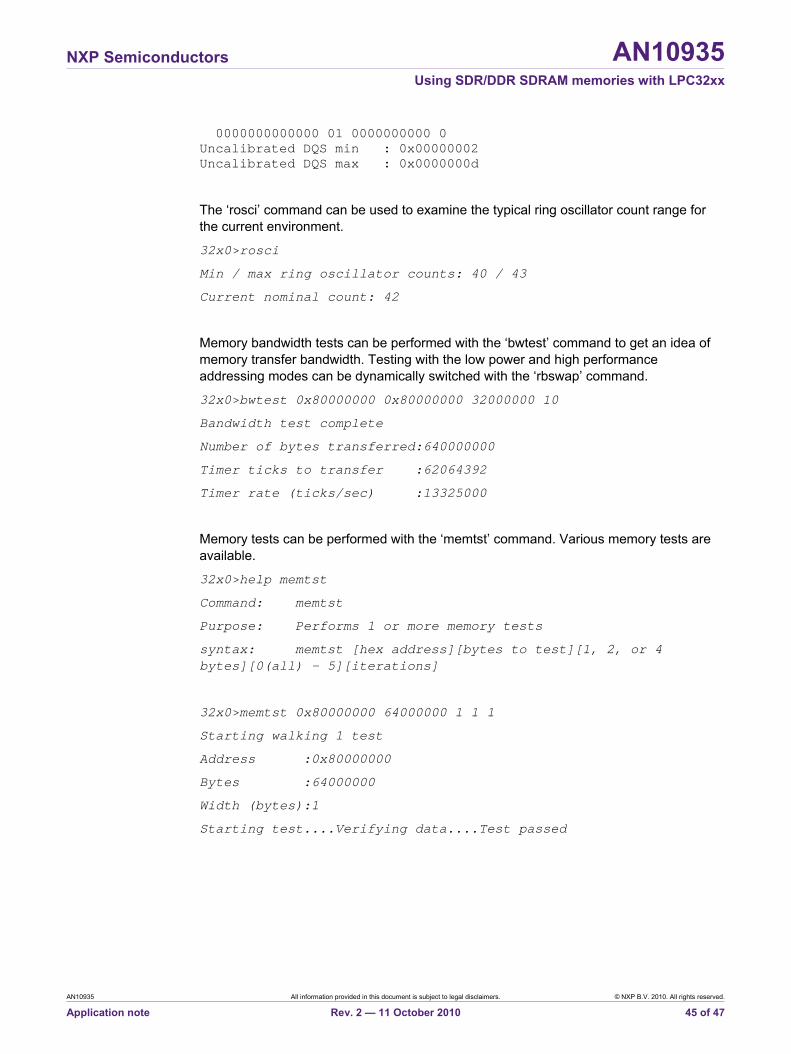
NXP Semiconductors AN10935 Using SDR/DDR SDRAM memories with LPC32xx
AN10935 All information provided in this document is subject to legal disclaimers. © NXP B.V. 2010. All rights reserved.
Application note Rev. 2 — 11 October 2010 45 of 47
0000000000000 01 0000000000 0 Uncalibrated DQS min : 0x00000002 Uncalibrated DQS max : 0x0000000d
The ‘rosci’ command can be used to examine the typical ring oscillator count range for the current environment.
32x0>rosci
Min / max ring oscillator counts: 40 / 43
Current nominal count: 42
Memory bandwidth tests can be performed with the ‘bwtest’ command to get an idea of memory transfer bandwidth. Testing with the low power and high performance addressing modes can be dynamically switched with the ‘rbswap’ command.
32x0>bwtest 0x80000000 0x80000000 32000000 10
Bandwidth test complete
Number of bytes transferred:640000000
Timer ticks to transfer :62064392
Timer rate (ticks/sec) :13325000
Memory tests can be performed with the ‘memtst’ command. Various memory tests are available.
32x0>help memtst
Command: memtst
Purpose: Performs 1 or more memory tests
syntax: memtst [hex address][bytes to test][1, 2, or 4 bytes][0(all) - 5][iterations]
32x0>memtst 0x80000000 64000000 1 1 1
Starting walking 1 test
Address :0x80000000
Bytes :64000000
Width (bytes):1
Starting test....Verifying data....Test passed
NXP Semiconductors AN10935 Using SDR/DDR SDRAM memories with LPC32xx
AN10935 All information provided in this document is subject to legal disclaimers. © NXP B.V. 2010. All rights reserved.
Application note Rev. 2 — 11 October 2010 46 of 47
4. Legal information
4.1 Definitions Draft — The document is a draft version only. The content is still under internal review and subject to formal approval, which may result in modifications or additions. NXP Semiconductors does not give any representations or warranties as to the accuracy or completeness of information included herein and shall have no liability for the consequences of use of such information.
4.2 Disclaimers Limited warranty and liability — Information in this document is believed to be accurate and reliable. However, NXP Semiconductors does not give any representations or warranties, expressed or implied, as to the accuracy or completeness of such information and shall have no liability for the consequences of use of such information.
In no event shall NXP Semiconductors be liable for any indirect, incidental, punitive, special or consequential damages (including - without limitation - lost profits, lost savings, business interruption, costs related to the removal or replacement of any products or rework charges) whether or not such damages are based on tort (including negligence), warranty, breach of contract or any other legal theory.
Notwithstanding any damages that customer might incur for any reason whatsoever, NXP Semiconductors’ aggregate and cumulative liability towards customer for the products described herein shall be limited in accordance with the Terms and conditions of commercial sale of NXP Semiconductors.
Right to make changes — NXP Semiconductors reserves the right to make changes to information published in this document, including without limitation specifications and product descriptions, at any time and without notice. This document supersedes and replaces all information supplied prior to the publication hereof.
Suitability for use — NXP Semiconductors products are not designed, authorized or warranted to be suitable for use in life support, life-critical or safety-critical systems or equipment, nor in applications where failure or malfunction of an NXP Semiconductors product can reasonably be expected to result in personal injury, death or severe property or environmental damage. NXP Semiconductors accepts no liability for inclusion and/or use of
NXP Semiconductors products in such equipment or applications and therefore such inclusion and/or use is at the customer’s own risk.
Applications — Applications that are described herein for any of these products are for illustrative purposes only. NXP Semiconductors makes no representation or warranty that such applications will be suitable for the specified use without further testing or modification.
Customers are responsible for the design and operation of their applications and products using NXP Semiconductors products, and NXP Semiconductors accepts no liability for any assistance with applications or customer product design. It is customer’s sole responsibility to determine whether the NXP Semiconductors product is suitable and fit for the customer’s applications and products planned, as well as for the planned application and use of customer’s third party customer(s). Customers should provide appropriate design and operating safeguards to minimize the risks associated with their applications and products.
NXP Semiconductors does not accept any liability related to any default, damage, costs or problem which is based on any weakness or default in the customer’s applications or products, or the application or use by customer’s third party customer(s). Customer is responsible for doing all necessary testing for the customer’s applications and products using NXP Semiconductors products in order to avoid a default of the applications and the products or of the application or use by customer’s third party customer(s). NXP does not accept any liability in this respect.
Export control — This document as well as the item(s) described herein may be subject to export control regulations. Export might require a prior authorization from national authorities.
4.3 Trademarks Notice: All referenced brands, product names, service names and trademarks are property of their respective owners.
NXP Semiconductors AN10935 Using SDR/DDR SDRAM memories with LPC32xx
Please be aware that important notices concerning this document and the product(s) described herein, have been included in the section 'Legal information'.
© NXP B.V. 2010. All rights reserved.
For more information, please visit: http://www.nxp.com For sales office addresses, please send an email to: [email protected]
Date of release: 11 October 2010Document identifier: AN10935
5. Contents
1. Introduction .........................................................3 2. External memory controller................................3 2.1 EMC pins............................................................4 2.2 Maximum system SDRAM memory ...................6 2.3 Contiguous SDRAM across EMC_DYCS0 and
EMC_DYCS1 .....................................................7 2.4 SDRAM clock enable when using EMC_DYCS0
and EMC_DYCS1 ..............................................7 2.5 SDR SDRAM connections..................................8 2.5.1 Routing rules for SDR SDRAM ..........................9 2.5.2 Function of EMC_CLKIN pin ............................10 2.5.2.1 EMC_CLKIN to compensate for long flight times
.........................................................................10 2.6 DDR SDRAM connections ...............................11 2.7 Routing rules for DDR SDRAM ........................13 2.7.1 Function of EMC_CLKIN pin ............................14 2.8 SDRAM layout optimization..............................14 2.9 Shared bus placement for SDRAM and Static
memory devices ...............................................14 2.10 Address mapping between AHB address and
SDR/DDR SDRAM...........................................14 2.11 Using 32-bit SDRAMs not in UM10326 Table 115
Address mapping .............................................23 2.12 Special cases connecting SDRAM BA[1:0] to
EMC_A[14:13]..................................................23 2.13 Loading the SDRAM Mode Register or Extended
Mode register ...................................................24 2.13.1 Example writing to Mobile SDRAM Mode
Register in 16-bit system memory....................26 2.13.2 Example writing to Mobile SDRAM Mode
Register in 32-bit system memory....................27 3. SDRAM controller programming and
operations..........................................................30 3.1 Typical SDRAM programming sequences .......30 3.1.1 Standard and low power SDR SDRAM
programming sequence ...................................30 3.1.2 DDR SDRAM programming sequence.............33 3.1.3 SDR and DDR SDRAM setup example code ...37 3.2 SDRAM operational notes................................37 3.2.1 Changing system clocking modes....................37 3.2.1.1 Changing clock rates and SDRAM impact .......37 3.2.1.2 SDRAM operation in direct-run mode ..............38 3.2.1.3 Self-refresh mode.............................................38 3.2.2 DDR SDRAM calibration ..................................38 3.2.2.1 LPC32x0 DDR calibration functionality ............39 3.2.2.2 Calibration coefficients and storage .................40
3.2.2.3 Calibration method ...........................................40 3.2.2.4 Example calibration values...............................42 3.3 Common programming problems .....................43 3.3.1 SDR and DDR SDRAM problems ....................43 3.3.2 DDR SDRAM problems....................................44 3.3.3 SDRAM initialization and debugging features
included in the LPC32x0 CDL ..........................44 4. Legal information ..............................................46 4.1 Definitions.........................................................46 4.2 Disclaimers.......................................................46 4.3 Trademarks ......................................................46 5. Contents.............................................................47