Embed Size (px)
Citation preview

FN8371Rev 3.00
December 12, 2016
ISL29035Integrated Digital Light Sensor with Interrupt
DATASHEET
The ISL29035 is an integrated ambient and infrared light-to-digital converter with I2C (SMBus compatible) Interface. Its advanced self-calibrated photodiode array emulates human eye response with excellent IR rejection. The on-chip ADC is capable of rejecting 50Hz and 60Hz flicker caused by artificial light sources. The Lux range select feature allows users to program the Lux range for optimized counts/Lux.
For ambient light sensing, an internal 16-bit ADC has been designed based upon the charge-balancing technique. The ADC conversion time is nominally 105ms and is user adjustable from 11µs to 105ms, depending on oscillator frequency and ADC resolution. In normal operation, typical current consumption is 57µA. In order to further minimize power consumption, two power-down modes have been provided. If polling is chosen over continuous measurement of light, the auto power-down function shuts down the whole chip after each ADC conversion for the measurement. The other power-down mode is controlled by software via the I2C interface. The power consumption can be reduced to less than 0.3µA when powered down.
The ISL29035 supports a software brownout condition detection. The device powers up with the brownout bit asserted until the host clears it through the I2C interface.
The ISL29035 supports a software and hardware interrupt that remains asserted until the host clears it through the I2C interface. Function of ADC conversion continues without stopping after interrupt is asserted.
Designed to operate on supplies from 2.25V to 3.63V with an I2C supply from 1.7V to 3.63V, the ISL29035 is specified for operation across the -40°C to +85°C ambient temperature range.
Features• Resolution . . . . . . . . . . . . . . . . . . . . . . . . . . . . . . . . . 16-bit ADC
• Wide dynamic range . . . . . . . . . . . . . . . . . . . . . . . . . .1:4,200,000
• Integrated noise reduction . . . . . . . . . . . . . . . . . . . . . 50/60Hz
• Close to human eye response with excellent IR/UV rejection
• Shutdown modes. . . . . . . . . . . . . . . . . . . .software and automatic
• Programmable interrupt threshold with persistence filter
• Supply current (typical) . . . . . . . . . . . . . . . . . . . . . . . . . . . 57µA
• Shutdown current (maximum) . . . . . . . . . . . . . . . . . . . 0.51µA
• I2C (SMB compatible) power supply . . . . . . . . . 1.7V to 3.63V
• Sensor power supply . . . . . . . . . . . . . . . . . . . . . 2.25V to 3.63V
• Operating temperature range. . . . . . . . . . . . . -40°C to +85°C
• Small form factor package . . . . . . . 6 Ld 1.5x1.6x0.75 ODFN
Applications• Mobile devices: smart phone, PDA, GPS
• Computing devices: notebook PC, MacBook, tablets
• Consumer devices: LCD-TV, digital camera
• Industrial and medical light sensing
Related Literature• AN1591, “Evaluation Hardware/Software Manual for ALS
and Proximity Sensor”
TABLE 1. KEY DIFFERENCES BETWEEN FAMILY OF PARTS
PART NUMBER ALS SENSING INTERRUPT PINNUMBER OF
PINS
ISL29034 Yes No 4 Ld
ISL29035 Yes Yes 6 Ld
FN8371 Rev 3.00 Page 1 of 17December 12, 2016
ISL29035
FIGURE 1. ISL29035 TYPICAL APPLICATION DIAGRAM FIGURE 2. NORMALIZED SPECTRAL RESPONSE FOR AMBIENT LIGHT SENSING
ISL29035MCU
1µF
SCL
SDA6
5
1
2
4
VDD
GND
SCL
SDA
GPIO
4.7k
INT
VDD_PULLUP
3NC
4.7k 4.7k
VDD100
0
0.2
0.4
0.6
0.8
1.0
1.2
300 400 500 600 700 800 900 1000 1100
WAVELENGTH (nm)
HUMAN EYE
AMBIENT LIGHT SENSOR
NO
RM
AL
IZE
D R
ES
PO
NS
E
FN8371 Rev 3.00 Page 2 of 17December 12, 2016
ISL29035
Block Diagram
FIGURE 3. BLOCK DIAGRAM
SCL
SDA6
5
INTEGRATING ADC
CMD Register
DATA Register
INTERRUPT
IREF
fOSC
COMMAND REGISTER
LIGHT DATA PROCESS
4
INT
2
GND
1
VDD
I2C/SMBPHOTODIODE ARRAY
R500k
Pin ConfigurationISL29035
(6 LD ODFN)TOP VIEW
1
2
3
6
5
4
SDA
SCL
INT
VDD
GND
NC
Pin DescriptionsPIN
NUMBER PIN NAME DESCRIPTION
1 VDD Positive supply
2 GND Ground pin
3 NC No connect
4 INT Interrupt pin; LOW for interrupt alarming. INT pin is an open-drain. INT remains asserted until the interrupt status bit is reset.
5 SCL I2C serial clock
6 SDA I2C serial data
Ordering InformationPART NUMBER(Notes 1, 2, 3)
TEMP RANGE(°C)
TAPE AND REEL(UNITS)
PACKAGE(RoHS COMPLIANT)
PKG.DWG. #
ISL29035IROZ-T7 -40 to +85 3k units 6 Ld ODFN L6.1.5x1.6
ISL29035IROZ-T7A -40 to +85 250 units 6 Ld ODFN L6.1.5x1.6
ISL29035EVAL1Z Evaluation Board
NOTES:
1. Please refer to TB347 for details on reel specifications.
2. These Intersil Pb-free plastic packaged products employ special Pb-free material sets; molding compounds/die attach materials and NiPdAu-Ag plate - e4 termination finish, which is RoHS compliant and compatible with both SnPb and Pb-free soldering operations. Intersil Pb-free products are MSL classified at Pb-free peak reflow temperatures that meet or exceed the Pb-free requirements of IPC/JEDEC J STD-020.
3. For Moisture Sensitivity Level (MSL), please see product information page for ISL29035. For more information on MSL, please see tech brief TB477.
FN8371 Rev 3.00 Page 3 of 17December 12, 2016
ISL29035
Absolute Maximum Ratings Thermal InformationVDD to GND . . . . . . . . . . . . . . . . . . . . . . . . . . . . . . . . . . . . . . . . . . . . . . +4.0VI2C Bus (SCL, SDA) and INT Pin Voltage. . . . . . . . . . . . . . . . . . -0.2V to 4.0VI2C Bus (SCL, SDA) and INT Pin Current. . . . . . . . . . . . . . . . . . . . . . . <10mAInput Voltage Slew Rate (Maximum) . . . . . . . . . . . . . . . . . . . . . . . . . . . 0.1V/µsESD Ratings
Human Body Model . . . . . . . . . . . . . . . . . . . . . . . . . . . . . . . . . . . . . . . . 3kV
Thermal Resistance (Typical) JA (°C/W)
6 Ld ODFN Package (Note 4) . . . . . . . . . . . . . . . . . . . . . 210Maximum Junction Temperature (TJMAX). . . . . . . . . . . . . . . . . . . . . . .+90°CStorage Temperature Range. . . . . . . . . . . . . . . . . . . . . . . .-40°C to +100°COperating Temperature . . . . . . . . . . . . . . . . . . . . . . . . . . . . . -40°C to +85°CPb-Free Reflow Profile . . . . . . . . . . . . . . . . . . . . . . . . . . . . . . . . . . see TB477
CAUTION: Do not operate at or near the maximum ratings listed for extended periods of time. Exposure to such conditions may adversely impact productreliability and result in failures not covered by warranty.
NOTE:4. JA is measured in free air with the component mounted on a high effective thermal conductivity test board with “direct attach” features. See Tech
Brief TB379.
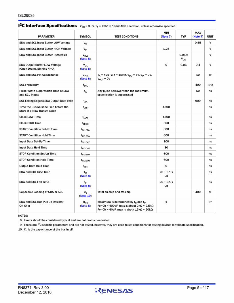
Electrical Specifications VDD = 3.0V, TA = +25°C, 16-bit ADC operation, unless otherwise specified.
DESCRIPTION PARAMETER TEST CONDITIONSMIN
(Note 7) TYPMAX
(Note 7) UNIT
Power Supply Range VDD 2.25 3.63 V
Supply Current IDD 57 85 µA
Supply Current when Powered Down IDD1 Software disabled or auto power-down 0.24 0.51 µA
Supply Voltage Range for I2C Interface VI2C 1.7 3.63 V
ADC Integration/Conversion Time tint 16-bit ADC data 105 ms
I2C Clock Rate Range FI2
C 400 kHz
Count Output when Dark DATA_0 E = 0 Lux, Range 0 (1k Lux) 1 5 Counts
Full Scale ADC Code DATA_F 65535 Counts
Part-to-Part Variation (3 Population) %/Value E = 300 Lux, cold white LED Range 0 (1k Lux)
±5 %
Light Count Output with LSB of 0.015 Lux/Count ADCR0 E = 300 Lux, cold white LED (Note 5), ALS Range 0 (1k Lux)
20473 Counts
Light Count Output with LSB of 0.06 Lux/Count ADCR1 E = 300 Lux, cold white LED (Note 5), ALS Range 1 (4k Lux)
5100 Counts
Light Count Output with LSB of 0.24 Lux/Count ADCR2 E = 300 Lux, cold white LED (Note 5), ALS Range 2 (16k Lux)
1400 Counts
Light Count Output with LSB of 0.96 Lux/Count ADCR3 E = 300 Lux, cold white LED (Note 5), ALS Range 3 (64k Lux)
366 Counts
Infrared Count Output (Note 6) ADC_IRR0 Range 0 (1k Lux) 1402 1997 2598 Counts
Infrared Count Output (Note 6) ADC_IRR1 Range 1 (4k Lux) 481 Counts
Infrared Count Output (Note 6) ADC_IRR2 Range 2 (16k Lux) 148 Counts
Infrared Count Output (Note 6) ADC_IRR3 Range 3 (64k Lux) 42 Counts
SDA Current Sinking Capability ISDA 4 5 mA
INT Current Sinking Capability IINT 4 5 mA
NOTES:
5. 550nm green LED is used in production test. The 550nm LED irradiance is calibrated to produce the same DATA count against an illuminance level of 300 Lux Cold White LED.
6. 850nm IR LED is used in production test. The 850nm LED irradiance is calibrated to produce the same DATA_IR count against and illuminance level of 210 lux sunlight at sea level.
7. Compliance to datasheet limits is assured by one or more methods: production test, characterization and/or design.
FN8371 Rev 3.00 Page 4 of 17December 12, 2016
ISL29035
I2C Interface Specifications VDD = 3.0V, TA = +25°C, 16-bit ADC operation, unless otherwise specified.
PARAMETER SYMBOL TEST CONDITIONSMIN
(Note 7) TYP MAX
(Note 7) UNIT
SDA and SCL Input Buffer LOW Voltage VIL 0.55 V
SDA and SCL Input Buffer HIGH Voltage VIH 1.25 V
SDA and SCL Input Buffer Hysteresis VHys(Note 8)
0.05 x VDD
V
SDA Output Buffer LOW Voltage (Open-Drain), Sinking 4mA
VOL(Note 8)
0 0.06 0.4 V
SDA and SCL Pin Capacitance CPIN(Note 8)
TA = +25°C, f = 1MHz, VDD = 5V, VIN = 0V, VOUT = 0V
10 pF
SCL Frequency fSCL 400 kHz
Pulse Width Suppression Time at SDA and SCL Inputs
tIN Any pulse narrower than the maximum specification is suppressed
50 ns
SCL Falling Edge to SDA Output Data Valid tAA 900 ns
Time the Bus Must be Free before the Start of a New Transmission
tBUF 1300 ns
Clock LOW Time tLOW 1300 ns
Clock HIGH Time tHIGH 600 ns
START Condition Set-Up Time tSU:STA 600 ns
START Condition Hold Time tHD:STA 600 ns
Input Data Set-Up Time tSU:DAT 100 ns
Input Data Hold Time tHD:DAT 30 ns
STOP Condition Set-Up Time tSU:STO 600 ns
STOP Condition Hold Time tHD:STO 600 ns
Output Data Hold Time tDH 0 ns
SDA and SCL Rise Time tR(Note 8)
20 + 0.1 x Cb
ns
SDA and SCL Fall Time tF(Note 8)
20 + 0.1 x Cb
ns
Capacitive Loading of SDA or SCL Cb(Note 10)
Total on-chip and off-chip 400 pF
SDA and SCL Bus Pull-Up Resistor Off-Chip
RPU(Note 8)
Maximum is determined by tR and tF. For Cb = 400pF, max is about 2kΩ ~ 2.5kΩFor Cb = 40pF, max is about 15kΩ ~ 20kΩ
1 k
NOTES:
8. Limits should be considered typical and are not production tested.
9. These are I2C specific parameters and are not tested, however, they are used to set conditions for testing devices to validate specification.
10. Cb is the capacitance of the bus in pF.
FN8371 Rev 3.00 Page 5 of 17December 12, 2016
ISL29035
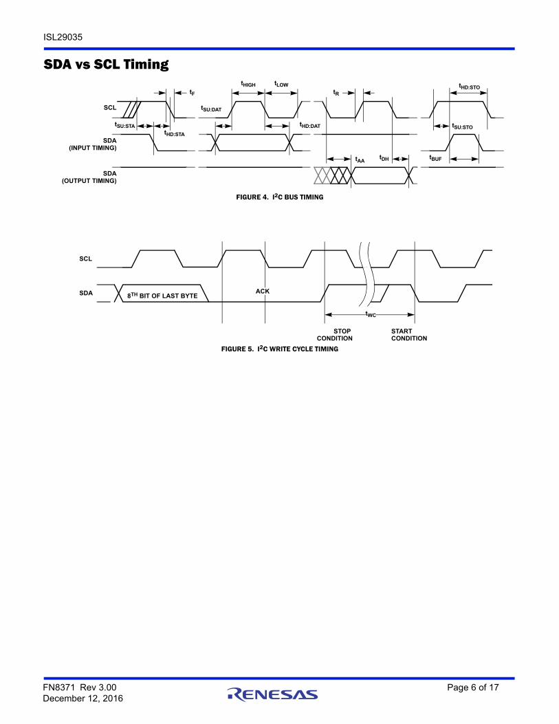
SDA vs SCL Timing
FIGURE 4. I2C BUS TIMING
FIGURE 5. I2C WRITE CYCLE TIMING
tSU:STO
tDH
tHIGH
tSU:STAtHD:STA
tHD:DAT
tSU:DATSCL
SDA(INPUT TIMING)
SDA(OUTPUT TIMING)
tF
tLOW
tBUFtAA
tRtHD:STO
STOP CONDITION
STARTCONDITION
tWC
ACK
SCL
SDA 8TH BIT OF LAST BYTE
FN8371 Rev 3.00 Page 6 of 17December 12, 2016
ISL29035
Typical Performance Curves
FIGURE 6. NORMALIZED SPECTRAL RESPONSE FOR AMBIENT LIGHT SENSING
FIGURE 7. NORMALIZED RADIATION PATTERN
FIGURE 8. TEMPERATURE TEST IN DARK CONDITION FIGURE 9. ALS TRANSFER FUNCTION
0
0.2
0.4
0.6
0.8
1.0
1.2
300 400 500 600 700 800 900 1000 1100
WAVELENGTH (nm)
HUMAN EYE
AMBIENT LIGHT SENSOR
NO
RM
AL
IZE
D R
ES
PO
NS
E
0
0.2
0.4
0.6
0.8
1.0
1.2
-60 -50 -40 -30 -20 -10 0 10 20 30 40 50 60
NO
RM
AL
IZE
D S
EN
SIT
IVIT
Y
ANGLE (°)
0
2
4
6
8
10
12
14
-60 -50 -40 -30 -20 -10 0 10 20 30 40 50 60 70 80 90 100
AL
S R
EA
DIN
G (
CO
UN
TS
)
TEMPERATURE (°C)
1000 LUX RANGE
0
200
400
600
800
1000
0 200 400 600 800 1000
AL
S M
EA
SU
RE
D (
LU
X)
AMBIENT LIGHT (LUX)
1000 LUX RANGE
FN8371 Rev 3.00 Page 7 of 17December 12, 2016
ISL29035
Principles of OperationPhotodiodes and ADCThe ISL29035 contains two photodiode arrays, which convert light into current. The spectral response for ambient light sensing is shown in Figure 6 on page 7. After light is converted to current during the light signal process, the current output is converted to digital by a built-in 16-bit Analog-to-Digital Converter (ADC). An I2C command reads the ambient light or IR intensity in counts.
The converter is a charge-balancing integrating type 16-bit ADC. The chosen method for conversion is best for converting small current signals in the presence of an AC periodic noise. A 105ms integration time, for instance, highly rejects 50Hz and 60Hz power line noise simultaneously.
The integration time of the built-in ADC is determined by the internal oscillator, and the n-bit (n = 4, 8, 12, 16) counter inside the ADC. A good balancing act of integration time and resolution (depending on the application) is required for optimal results.
The ADC has I2C programmable range select to dynamically accommodate various lighting conditions. For very dim conditions, the ADC can be configured at its lowest range (Range 0) in the ambient light sensing.
Low-Power OperationThe ISL29035 initial operation is at the power-down mode after a supply voltage is provided. The data registers contain the default value of 0. When the ISL29035 receives an I2C command to do a one-time measurement from an I2C master, it will start ADC conversion with light sensing. The ISL29035 will go to the power-down mode automatically after one conversion is finished and keep the conversion data available for the master to fetch anytime afterwards. When receiving an I2C command of continuous measurement, the device will continuously do ADC conversions with light sensing and will continuously update the data registers with the latest conversion data. The device will go into power-down mode after receiving the power-down I2C command.
Ambient Light and IR SensingThere are four operational modes in ISL29035: Programmable ALS once with auto power-down, programmable IR sensing once with auto power-down, programmable continuous ALS sensing and programmable continuous IR sensing. These four modes can be programmed in series to fulfill the application needs. The detailed program configuration is listed in “Command-I Register (Address: 0x00)” on page 11.
When the part is programmed for ambient light sensing, the ambient light wavelength within the “Ambient Light Sensing” spectral response curve in Figure 15 is converted into current. With ADC, the current is converted to an unsigned n-bit (up to 16 bits) digital output.
When the part is programmed for Infrared (IR) sensing, the IR light wavelength within the “IR Sensing” spectral response curve in Figure 15 is converted into current. With ADC, the current is converted to an unsigned n-bit (up to 16 bits) digital output.
Interrupt FunctionThe active low interrupt pin is an open-drain pull-down configuration. The interrupt pin serves as an alarm or monitoring function to determine whether the ambient light level exceeds the upper threshold or goes below the lower threshold. It should be noted that the function of ADC conversion continues without stopping after interrupt is asserted. If the user needs to read the ADC count that triggers the interrupt, the reading should be done before the data registers are refreshed by the following conversions. The user can also configure the persistence of the interrupt pin. This reduces the possibility of false triggers, such as noise or sudden spikes in ambient light conditions. An unexpected camera flash, for example, can be ignored by setting the persistence to 8 integration cycles.
Serial InterfaceThe ISL29035 supports the Inter-Integrated Circuit (I2C) bus data transmission protocol. The I2C bus is a two-wire serial bidirectional interface consisting of SCL (Clock) and SDA (Data). Both the wires are connected to the device supply via pull-up resistors. The I2C protocol defines any device that sends data onto the bus as a transmitter and the receiving device as the receiver. The device controlling the transfer is a master and the device being controlled is the slave. The transmitting device pulls down the SDA line to transmit a “0” and releases it to transmit a “1”. The master always initiates the data transfer, only when the bus is not busy, and provides the clock for both transmitting and receiving operations. The ISL29035 operates as a slave device in all applications. The serial communication over the I2C interface is conducted by sending the Most Significant Bit (MSB) of each byte of data first.
Start ConditionDuring data transfer, the SDA line must remain stable while the SCL line is HIGH. All I2C interface operations must begin with a START condition, which is a HIGH to LOW transition of SDA while SCL is HIGH (refer to Figure 12 on page 9). The ISL29035 continuously monitors the SDA and SCL lines for the START condition and does not respond to any command until this condition is met (refer to Figure 12). A START condition is ignored during the power-up sequence.
Stop ConditionAll I2C interface operations must be terminated by a STOP condition, which is a LOW to HIGH transition of SDA while SCL is HIGH (refer to Figure 12). A STOP condition at the end of a read/write operation places the device in its standby mode. If a stop is issued in the middle of a Data byte, or before 1 full Data byte + ACK is sent, then the serial communication of the ISL29035 resets itself without performing the read/write. The contents of the array are not affected.
AcknowledgeAn Acknowledge (ACK) is a software convention used to indicate a successful data transfer. The transmitting device releases the SDA bus after transmitting 8 bits. During the ninth clock cycle, the receiver pulls the SDA line LOW to acknowledge the reception of the 8 bits of data (refer to Figure 12). The ISL29035 responds with an ACK after recognition of a START condition followed by a
FN8371 Rev 3.00 Page 8 of 17December 12, 2016
ISL29035
valid Identification Byte, and once again, after successful receipt of an Address Byte. The ISL29035 also responds with an ACK after receiving a Data byte of a write operation. The master must respond with an ACK after receiving a Data byte of a read operation.
Device AddressingFollowing a START condition, the master must output a Device Address byte. The 7 MSBs of the Device Address byte are known as the device identifier. The device identifier bits of the ISL29035 are internally hard-wired as “1000100”. The LSB of the Device Address byte is defined as a Read or Write (R/W) bit. When this R/W bit is a “1”, a read operation is selected and when “0”, a write operation is selected (refer to Figure 10). The master generates a START condition followed by Device Address byte 1000100x (x as R/W) and the ISL29035 compares it with the internal device identifier. Upon a correct comparison, the device outputs an acknowledge (LOW) on the SDA line (refer to Figure 12).
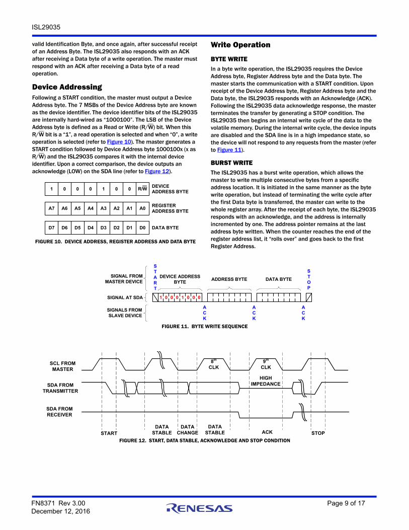
Write Operation
BYTE WRITEIn a byte write operation, the ISL29035 requires the Device Address byte, Register Address byte and the Data byte. The master starts the communication with a START condition. Upon receipt of the Device Address byte, Register Address byte and the Data byte, the ISL29035 responds with an Acknowledge (ACK). Following the ISL29035 data acknowledge response, the master terminates the transfer by generating a STOP condition. The ISL29035 then begins an internal write cycle of the data to the volatile memory. During the internal write cycle, the device inputs are disabled and the SDA line is in a high impedance state, so the device will not respond to any requests from the master (refer to Figure 11).
BURST WRITEThe ISL29035 has a burst write operation, which allows the master to write multiple consecutive bytes from a specific address location. It is initiated in the same manner as the byte write operation, but instead of terminating the write cycle after the first Data byte is transferred, the master can write to the whole register array. After the receipt of each byte, the ISL29035 responds with an acknowledge, and the address is internally incremented by one. The address pointer remains at the last address byte written. When the counter reaches the end of the register address list, it “rolls over” and goes back to the first Register Address.
FIGURE 10. DEVICE ADDRESS, REGISTER ADDRESS AND DATA BYTE
DEVICE ADDRESS BYTE
REGISTER ADDRESS BYTE
DATA BYTE
1 0 0 0 1 0 0 R/W
A7 A6 A5 A4 A3 A2 A1 A0
D7 D6 D5 D4 D3 D2 D1 D0
FIGURE 11. BYTE WRITE SEQUENCE
1 0 0 0 1 0 0 0
ACK
ACK
ACK
STOP
START
DEVICE ADDRESS BYTE
ADDRESS BYTE DATA BYTESIGNAL FROM
MASTER DEVICE
SIGNAL AT SDA
SIGNALS FROM SLAVE DEVICE
FIGURE 12. START, DATA STABLE, ACKNOWLEDGE AND STOP CONDITION
SDA FROM RECEIVER
SDA FROM TRANSMITTER
SCL FROM MASTER
STARTDATA
CHANGEDATA
STABLEDATA
STABLE ACK STOP
8th CLK
9th CLK
HIGH IMPEDANCE
FN8371 Rev 3.00 Page 9 of 17December 12, 2016
ISL29035
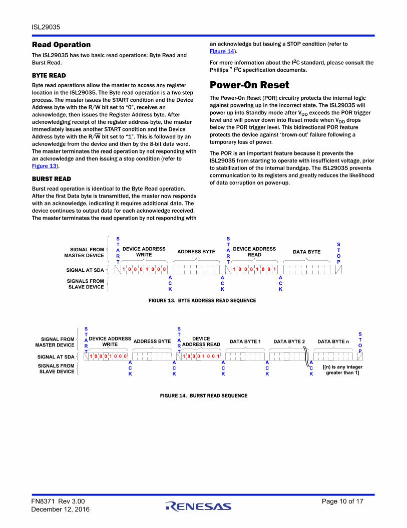
Read OperationThe ISL29035 has two basic read operations: Byte Read and Burst Read.
BYTE READByte read operations allow the master to access any register location in the ISL29035. The Byte read operation is a two step process. The master issues the START condition and the Device Address byte with the R/W bit set to “0”, receives an acknowledge, then issues the Register Address byte. After acknowledging receipt of the register address byte, the master immediately issues another START condition and the Device Address byte with the R/W bit set to “1”. This is followed by an acknowledge from the device and then by the 8-bit data word. The master terminates the read operation by not responding with an acknowledge and then issuing a stop condition (refer to Figure 13).
BURST READBurst read operation is identical to the Byte Read operation. After the first Data byte is transmitted, the master now responds with an acknowledge, indicating it requires additional data. The device continues to output data for each acknowledge received. The master terminates the read operation by not responding with
an acknowledge but issuing a STOP condition (refer to Figure 14).
For more information about the I2C standard, please consult the Phillips™ I2C specification documents.
Power-On ResetThe Power-On Reset (POR) circuitry protects the internal logic against powering up in the incorrect state. The ISL29035 will power up into Standby mode after VDD exceeds the POR trigger level and will power down into Reset mode when VDD drops below the POR trigger level. This bidirectional POR feature protects the device against ‘brown-out’ failure following a temporary loss of power.
The POR is an important feature because it prevents the ISL29035 from starting to operate with insufficient voltage, prior to stabilization of the internal bandgap. The ISL29035 prevents communication to its registers and greatly reduces the likelihood of data corruption on power-up.
1 0 0 0 1 0 0 0
ACK
ACK
START
DEVICE ADDRESS WRITE
ADDRESS BYTESIGNAL FROM MASTER DEVICE
SIGNAL AT SDA
SIGNALS FROM SLAVE DEVICE
ACK
STOP
DEVICE ADDRESS READ
DATA BYTE
START
1 0 0 0 1 0 0 1
FIGURE 13. BYTE ADDRESS READ SEQUENCE
FIGURE 14. BURST READ SEQUENCE
1 0 0 0 1 0 0 0ACK
ACK
START
DEVICE ADDRESS WRITE
ADDRESS BYTESIGNAL FROM MASTER DEVICE
SIGNAL AT SDA
SIGNALS FROM SLAVE DEVICE
ACK
STOP
DEVICE ADDRESS READ
DATA BYTE 1
START
1 0 0 0 1 0 0 1ACK
DATA BYTE 2
ACK
DATA BYTE n
[(n) is any integer greater than 1]
FN8371 Rev 3.00 Page 10 of 17December 12, 2016
ISL29035
Register DescriptionFollowing are detailed descriptions of the control registers related to the operation of the ISL29035 ambient light sensor device. These registers are accessed by the I2C serial interface. For details on the I2C interface, refer to “Serial Interface” on page 8.
All the features of the device are controlled by the registers. The ADC data can also be read. The following sections explain the details of each register bit. All RESERVED bits are Intersil used bits ONLY. The value of the reserved bit can change without notice.
Decimal to Hexadecimal ConversionTo convert decimal value to hexadecimal value, divide the decimal number by 16 and write the remainder on the side as the least significant digit. This process is continued by dividing the quotient by 16 and writing the remainder until the quotient is 0. When performing the division, the remainders, which will represent the hexadecimal equivalent of the decimal number, are written beginning with the least significant digit (right) and each new digit is written to the next most significant digit (the left) of the previous digit. Consider the number 175 decimal.
Command-I Register (Address: 0x00)
The Command-I register consists of control and status bits. In this register, there are two interrupt persist bits, one interrupt status bit and three operation mode bits. The operation mode bits and the interrupt persist bits are independent of each other. The default register value is 0x00 at power-on.
INTERRUPT PERSIST BITS (B0-B1)The interrupt persist bits provide control over when interrupts occur. There are four different selections for this feature. A value of n (where n is 1, 4, 8, and 16) results in an interrupt only if the value remains outside the threshold window for n consecutive integration cycles. For example, if n is equal to 16 and the ADC resolution is set to 16-bits, then the integration time is 105ms. An interrupt is generated whenever the last conversion results in a value outside of the programmed threshold window. The interrupt is active-low and remains asserted until cleared by writing the COMMAND register with the CLEAR bit set. Table 5 lists the possible interrupt persist bits.
INTERRUPT STATUS BIT (B2)The interrupt status bit (INT) is a status bit for light intensity detection. The bit is set to logic HIGH when the light intensity crosses the interrupt thresholds window (register address 0x04 - 0x07), and set to logic LOW when it is within the interrupt thresholds window. Once the interrupt is triggered, the INT pin goes low and the interrupt status bit goes HIGH until the status bit is polled through the I2C read command. Both the INT pin and the interrupt status bit are automatically cleared at the end of the 8-bit Device Register byte (0x00) transfer. Table 6 shows the interrupt status states.
TABLE 2. REGISTER MAP
NAME
REGISTER ADDRESS REGISTER BITS
DEFAULT ACCESSDEC HEX B7 B6 B5 B4 B3 B2 B1 B0
COMMAND-I 0 0x00 OP2 OP1 OP0 RESERVED INT PRST1 PRST0 0x00 RW
COMMAND-II 1 0x01 RESERVED RES1 RES0 RANGE1 RANGE0 0x00 RW
DATALSB 2 0x02 D7 D6 D5 D4 D3 D2 D1 D0 0x00 RO
DATAMSB 3 0x03 D15 D14 D13 D12 D11 D10 D9 D8 0x00 RO
INT_LT_LSB 4 0x04 TL7 TL6 TL5 TL4 TL3 TL2 TL1 TL0 0x00 RW
INT_LT_MSB 5 0x05 TL15 TL14 TL13 TL12 TL11 TL10 TL9 TL8 0x00 RW
INT_HT_LSB 6 0x06 TH7 TH6 TH5 TH4 TH3 TH2 TH1 TH0 0xFF RW
INT_HT_MSB 7 0x07 TH15 TH14 TH13 TH12 TH11 TH10 TH9 TH8 0xFF RW
ID 15 0x0F BOUT RESERVED 1 0 1 RESERVED 1x101xxx RW
TABLE 3. DECIMAL TO HEXADECIMAL
DIVISION QUOTIENT REMAINDER HEX NUMBER
175/16 10 = A 15 = F 0xAF
TABLE 4. COMMAND-I REGISTER ADDRESS
NAMEADDR(HEX)
REGISTER BITSDFLT(HEX)B7 B6 B5 B4 B3 B2 B1 B0
COMMAND-I 0x00 OP2
OP1
OP0
RESERVED INT PRST1
PRST0
0x00
TABLE 5. INTERRUPT PERSIST BITS
B1 B0NUMBER OF INTEGRATION
CYCLES (n)
0 0 1
0 1 4
1 0 8
1 1 16
TABLE 6. INTERRUPT STATUS BIT (INT)
BIT 2 OPERATION
0 Interrupt is cleared or not triggered yet
1 Interrupt is triggered
FN8371 Rev 3.00 Page 11 of 17December 12, 2016
ISL29035
OPERATION MODE BITS (B5-B7)The ISL29035 has different operating modes. These modes are selected by setting B5 - B7 bits on register address 0x00. The device powers up on a disable mode. Table 7 lists the possible operating modes.
Command-II Register (Address: 0x01)
The Command-II register consists of ADC control bits. In this register, there are two range bits and two ADC resolution bits. The default register value is 0x00 at power-on.
FULL SCALE LUX RANGE (B0-B1)The full scale Lux range has four different selectable ranges. The range determines the full scale Lux range (1k, 4k, 16k and 64k). Each range has a maximum allowable Lux value. Lower range values offer better resolution. Table 9 lists the possible values of Lux.
ADC RESOLUTION (B3-B2)B2 and B3 determine the ADC’s resolution and the number of clock cycles per conversion. Changing the number of clock cycles does more than just change the resolution of the device; it also
changes the integration time, which is the period the device’s Analog-to-Digital (A/D) converter samples the photodiode current signal for a measurement. Table 10 lists the possible ADC resolution. Only 16-bit ADC resolution can reject better 50/60Hz noise flickering light source.
Integration Time
Data Registers (Addresses: 0x02 and 0x03)
The ISL29035 has two 8-bit read-only registers to hold the upper and lower byte of the ADC value. The upper byte is accessed at address 0x03 and the lower byte is accessed at address 0x02. For 16-bit resolution, the data is from D0 to D15; for 12-bit resolution, the data is from D0 to D11; for 8-bit resolution, the data is from D0 to D7 and for 4-bit resolution, the data is from D0 to D3. The registers are refreshed after every conversion cycle. The default register value is 0x00 at power-on.
TABLE 7. OPERATING MODES BITS
B7 B6 B5 OPERATION
0 0 0 Power-down the device (default)
0 0 1 The device measures ALS only once every integration cycle. This is the lowest operating mode. (Note 11)
0 1 0 IR once
0 1 1 Reserved (Do Not Use)
1 0 0 Reserved (Do Not Use)
1 0 1 Measures ALS continuously
1 1 0 Measures IR continuous
1 1 1 Reserved (Do Not Use)
NOTE:11. Intersil does not recommend using this mode.
TABLE 8. COMMAND-II REGISTER BITS
NAMEADDR(HEX)
REGISTER BITS
DFLT(HEX)
B7
B6
B5
B4 B3 B2 B1 B0
COMMAND-II 0x01 RESERVED RES1
RES0
RANGE1
RANGE0
0x00
TABLE 9. RANGE REGISTER BITS
RANGE SELECTION B1 B0FULL SCALE LUX RANGE
(Lux)
0 0 0 1,000
1 0 1 4,000
2 1 0 16,000
3 1 1 64,000
TABLE 10. ADC RESOLUTION DATA WIDTH
B3 B2 NUMBER OF CLOCK CYCLES n-BIT ADC
0 0 216 = 65,536 16
0 1 212 = 4,096 12
1 0 28 = 256 8
1 1 24 = 16 4
TABLE 11. INTEGRATION TIME OF n-BIT ADC
n # ADC BITS INTEGRATION TIME (ms)
4 0.0256
8 0.41
12 6.5
16 105
TABLE 12. ADC REGISTER BITS
NAMEADDR(HEX)
REGISTER BITSDFLT(HEX)B7 B6 B5 B4 B3 B2 B1 B0
DATALSB 0x02 D7 D6 D5 D4 D3 D2 D1 D0 0x00
DATAMSB 0x03 D15 D14 D13 D12 D11 D10 D9 D8 0x00
TABLE 13. ADC DATA REGISTERS
ADDRESS(HEX) CONTENTS
0x02 D0 is LSB for 4-, 8-, 12- or 16-bit resolution; D3 is MSB for 4-bit resolution; D7 is MSB for 8-bit resolution
0x03 D15 is MSB for 16-bit resolution; D11 is MSB for 12-bit resolution
FN8371 Rev 3.00 Page 12 of 17December 12, 2016
ISL29035
Lower Interrupt Threshold Registers (Address: 0x04 and 0x05)
The lower interrupt threshold registers are used to set the lower trigger point for interrupt generation. If the ALS value crosses below or is equal to the lower threshold, an interrupt is asserted on the interrupt pin and the interrupt status. Registers INT_LT_LSB (0x04) and INT_LT_MSB (0x05) provide the LOW and HIGH bytes, respectively, of the lower interrupt threshold. The HIGH and LOW bytes from each set of registers are combined to form a 16-bit threshold value. The interrupt threshold registers default to 0x00 upon power-up.
Upper Interrupt Threshold Registers (Address: 0x06 and 0x07)
The upper interrupt threshold registers are used to set the upper trigger point for interrupt generation. If the ALS value crosses above or is equal to the upper threshold, an interrupt is asserted on the interrupt pin and the interrupt status. Registers INT_HT_LSB (0x06) and INT_HT_MSB (0x07) provide the LOW and HIGH bytes, respectively, of the upper interrupt threshold. The HIGH and LOW bytes from each set of registers are combined to form a 16-bit threshold value. The interrupt threshold registers default to 0xFF on power-up.
ID Register (Address: 0x0F)
The ID register has three different types of information, which is discussed in the following.
RESERVED BITS (B0-B2 AND B6)All RESERVED bits on the ISL29035 are Intersil used bits only. Bit0-Bit2 and Bit6 are RESERVED bits where their value might change without any notification to the user. It is advised when using the identification bits to identify the device in a system, the
software should mask the Bit0-Bit2 and Bit6-Bit7 to properly identify the device.
DEVICE ID BITS (B3-B5)The ISL29035 provides 3 bits to identify the device in a system. These bits are located on register address 0x0F, Bit3–Bit5. The identification bit value for the ISL29035 is xx101xxx. The device identification bits are read only bits. It is important to notice that Bit7 is a status bit for Brownout condition (BOUT).
BROWNOUT STATUS BIT - BOUT (B7)Bit7 on register address 0x0F is a status bit for Brownout condition (BOUT). The default value of this bit is “BOUT = 1” during the initial power-up, which indicates the device may possibly have gone through a brownout condition. Therefore, the status bit should be reset to “BOUT = 0” by an I2C write command during the initial configuration of the device.
The default register value is 0xA8 at power-on.
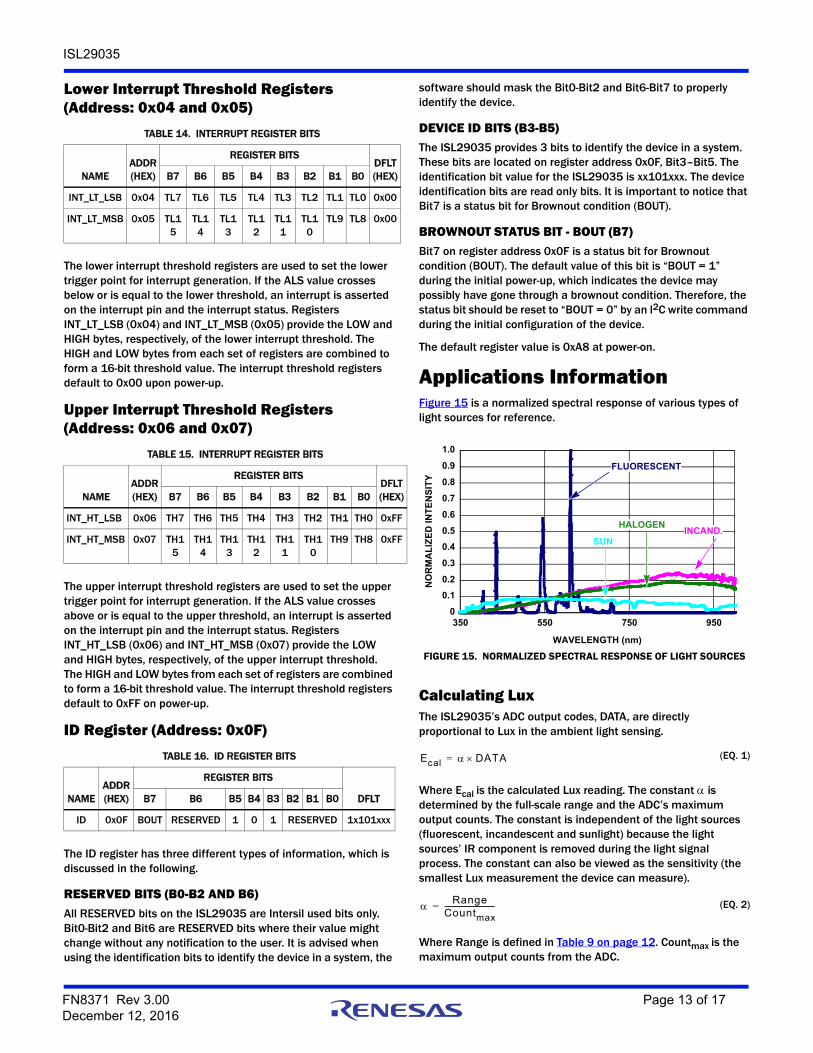
Applications InformationFigure 15 is a normalized spectral response of various types of light sources for reference.
Calculating LuxThe ISL29035’s ADC output codes, DATA, are directly proportional to Lux in the ambient light sensing.
Where Ecal is the calculated Lux reading. The constant is determined by the full-scale range and the ADC’s maximum output counts. The constant is independent of the light sources (fluorescent, incandescent and sunlight) because the light sources’ IR component is removed during the light signal process. The constant can also be viewed as the sensitivity (the smallest Lux measurement the device can measure).
Where Range is defined in Table 9 on page 12. Countmax is the maximum output counts from the ADC.
TABLE 14. INTERRUPT REGISTER BITS
NAMEADDR(HEX)
REGISTER BITSDFLT(HEX)B7 B6 B5 B4 B3 B2 B1 B0
INT_LT_LSB 0x04 TL7 TL6 TL5 TL4 TL3 TL2 TL1 TL0 0x00
INT_LT_MSB 0x05 TL15
TL14
TL13
TL12
TL11
TL10
TL9 TL8 0x00
TABLE 15. INTERRUPT REGISTER BITS
NAMEADDR(HEX)
REGISTER BITSDFLT(HEX)B7 B6 B5 B4 B3 B2 B1 B0
INT_HT_LSB 0x06 TH7 TH6 TH5 TH4 TH3 TH2 TH1 TH0 0xFF
INT_HT_MSB 0x07 TH15
TH14
TH13
TH12
TH11
TH10
TH9 TH8 0xFF
TABLE 16. ID REGISTER BITS
NAMEADDR(HEX)
REGISTER BITS
DFLTB7 B6 B5 B4 B3 B2 B1 B0
ID 0x0F BOUT RESERVED 1 0 1 RESERVED 1x101xxx
FIGURE 15. NORMALIZED SPECTRAL RESPONSE OF LIGHT SOURCES
0
0.1
0.2
0.3
0.4
0.5
0.6
0.7
0.8
0.9
1.0
350 550 750 950
WAVELENGTH (nm)
NO
RM
AL
IZE
D I
NT
EN
SIT
Y
FLUORESCENT
SUNINCAND.
HALOGEN
Ecal DATA= (EQ. 1)
RangeCountmax----------------------------= (EQ. 2)
FN8371 Rev 3.00 Page 13 of 17December 12, 2016
ISL29035
The transfer function used for n-bits ADC becomes Equation 3:
Where n = 4, 8, 12 or 16. This is the number of ADC bits programmed in the command register. 2n represents the maximum number of counts possible from the ADC output. Data is the ADC output stored in the data registers (02 hex and 03 hex).
Enhancing EV AccuracyThe device has an on-chip passive optical filter designed to block (reject) most of the incident Infrared. However, EV measurement may vary under differing IR-content light sources. In order to optimize the measurement variation between differing IR-content light sources, ISL29035 provides IR channel, which is programmed at COMMAND-I (Reg0x0) to measure the IR level of differing IR-content light sources.
The ISL29035’s ADC output codes, DATA, are directly proportional to the IR intensity received in the IR sensing.
Then EVAccuracy can be found in Equation 5:
Where DATAEV is the received ambient light intensity ADC output codes. K is a resolution of visible portion. Its unit is Lux/count. The typical value of K is 0.82. DATAIR is the received IR intensity. The constant changes with the spectrum of background IR, such as A, F2 and D65. The also changes with the ADC’s range and resolution selections. A typical for Range1 and Range2 is -11292.86 and for Range3 and Range4 it is 2137.14 without IR tinted glass.
Noise RejectionElectrical AC power worldwide is distributed at either 50Hz or 60Hz. Artificial light sources vary in intensity at the AC power frequencies. The undesired interference frequencies are infused on the electrical signals. This variation is one of the main sources of noise for the light sensors. Integrating type ADC’s have excellent noise-rejection characteristics for periodic noise sources whose frequency is an integer multiple of the conversion rate. By setting the sensor’s integration time to an integer multiple of periodic noise signal, the performance of an ambient light sensor can be improved greatly in the presence of noise. In order to reject the AC noise, the integration time of the sensor must be adjusted to match the AC noise cycle. For instance, a 60Hz AC unwanted signal’s sum from 0ms to k*16.66ms (k = 1,2...ki) is zero. Similarly, setting the device’s integration time to be an integer multiple of the periodic noise signal, greatly improves the light sensor output signal in the presence of noise.
Suggested PCB FootprintIt is important that users check the TB477, “Surface Mount Assembly Guidelines for Optical Dual Flat Pack No Lead (ODFN) Package” before starting ODFN product board mounting.
Board Mounting ConsiderationsFor applications requiring the light measurement, the board mounting location should be reviewed. The device uses an Optical Dual Flat Pack No Lead (ODFN) package, which subjects the die to mild stresses when the Printed Circuit (PC) board is heated and cooled, which slightly changes the shape. Because of these die stresses, placing the device in areas subject to slight twisting can cause degradation of reference voltage accuracy. It is normally best to place the device near the edge of a board, or on the shortest side, because the axis of bending is most limited in that location.
Layout ConsiderationsThe ISL29035 is relatively insensitive to layout. Like other I2C devices, it is intended to provide excellent performance even in significantly noisy environments. There are only a few considerations that will ensure best performance.
Route the supply and I2C traces as far as possible from all sources of noise. Use two power-supply decoupling capacitors, 1µF and 0.1µF, placed close to the device.
Soldering ConsiderationsConvection heating is recommended for reflow soldering; direct infrared heating is not recommended. The plastic ODFN package does not require a custom reflow soldering profile, and is qualified to +260°C. A standard reflow soldering profile with a +260°C maximum is recommended.
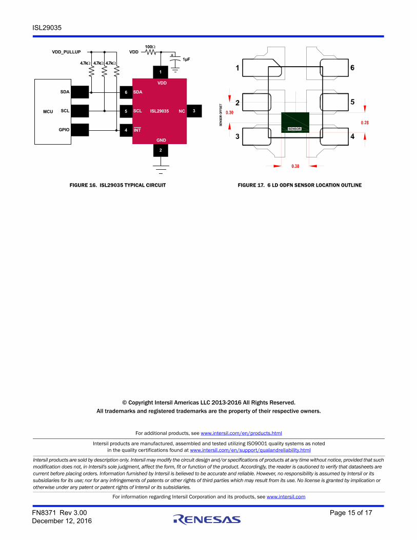
Typical CircuitA typical application for the ISL29035 is shown in Figure 16 on page 15. The ISL29035’s I2C address is internally hard-wired as 1000100. The device can be tied onto a system’s I2C bus, together with other I2C compliant devices.
(EQ. 3)EcalRange
2n
------------------- DATA=
DATAIR EIR= (EQ. 4)
EVAccuracy KxDATAEV DATAIR+= (EQ. 5)
FN8371 Rev 3.00 Page 14 of 17December 12, 2016
ISL29035
Intersil products are manufactured, assembled and tested utilizing ISO9001 quality systems as notedin the quality certifications found at www.intersil.com/en/support/qualandreliability.html
Intersil products are sold by description only. Intersil may modify the circuit design and/or specifications of products at any time without notice, provided that such modification does not, in Intersil's sole judgment, affect the form, fit or function of the product. Accordingly, the reader is cautioned to verify that datasheets are current before placing orders. Information furnished by Intersil is believed to be accurate and reliable. However, no responsibility is assumed by Intersil or its subsidiaries for its use; nor for any infringements of patents or other rights of third parties which may result from its use. No license is granted by implication or otherwise under any patent or patent rights of Intersil or its subsidiaries.
For information regarding Intersil Corporation and its products, see www.intersil.com
For additional products, see www.intersil.com/en/products.html
© Copyright Intersil Americas LLC 2013-2016 All Rights Reserved.All trademarks and registered trademarks are the property of their respective owners.
FIGURE 16. ISL29035 TYPICAL CIRCUIT FIGURE 17. 6 LD ODFN SENSOR LOCATION OUTLINE
ISL29035MCU
1µF
SCL
SDA6
5
1
2
4
VDD
GND
SCL
SDA
GPIO
4.7k
INT
VDD_PULLUP
3NC
4.7k 4.7k
VDD100
SENSOR
SEN
SOR
OFF
SE
T
FN8371 Rev 3.00 Page 15 of 17December 12, 2016
ISL29035
About IntersilIntersil Corporation is a leading provider of innovative power management and precision analog solutions. The company's products address some of the largest markets within the industrial and infrastructure, mobile computing and high-end consumer markets.
For the most updated datasheet, application notes, related documentation and related parts, please see the respective product information page found at www.intersil.com.
You may report errors or suggestions for improving this datasheet by visiting www.intersil.com/ask.
Reliability reports are also available from our website at www.intersil.com/support.
Revision History The revision history provided is for informational purposes only and is believed to be accurate, however, not warranted. Please go to web to make sure you have the latest revision.
DATE REVISION CHANGE
December 12, 2016 FN8371.3 Updated related literature on page 1.Added Table 1 on page 1.Added Note 6 on page 4 and referenced it in EC table.Removed Note 7 on page 3.Updated y-axis titles and added labels of Figures 7, 8 and 9. Updated title of Figure 9 (removed under F2 light source) on page 7.
December 24, 2015 FN8371.2 Removed sections “Digital Inputs and Termination” and “Temperature Coefficient” from “Applications Information” on page 13.Added Related Literature on page 1Updated Ordering Information table on page 3 by adding T&R quantity column and adding T7A partRemoved IR sensing from Figure 6 on page 7 and from “Photodiodes and ADC” on page 8 Removed 4 notes that were unrelated from Electrical Specifications table on page 4 and removed note referencing removed notes from paragraph after Equation 5 on page 14.Updated POD L6.1.5x1.6 to most current revision with rev change listed as follows:Tiebar Note updatedFrom: Tiebar shown (if present) is a non-functional feature.To: Tiebar shown (if present) is a non-functional feature and may be located on any of the 4 sides (or ends).
November 12, 2014 FN8371.1 On page 1 updated: 90ms to 105ms and changed Shutdown current from 0.3 to 0.51 and corrected the Labels on Figure 2.Updated the Ordering Information on page 3.On page 3 updated pin configuration to show that Pin 1 is the longest pin.In “Electrical Specifications” on page 4 updated:- “Light Source Variation” to “Part-to-part Variation”.- test conditions for %/Value, ADCR0, ADCR1,ADCR2, ADCR3, ADC_IRR0, ADC_IRR1,ADC_IRR2, and ADC_IRR3On page 7 corrected the labels on Figure 6.On page 8 updated:- under Photodiodes and ADC section Figure reference, changed from 100ms to 105ms, changed from Range 1 to Range 0.On page 11 under Interrupt Persist Bits (B0-B1) section, updated from 100ms to 105msOn page 12 added note for Table 7 and verbiage under ADC Resolution (B3-B2) sectionOn page 14 updated the Temperature Coefficient section.
September 18, 2013 FN8371.0 Initial Release.
FN8371 Rev 3.00 Page 16 of 17December 12, 2016
ISL29035
FN8371 Rev 3.00 Page 17 of 17December 12, 2016
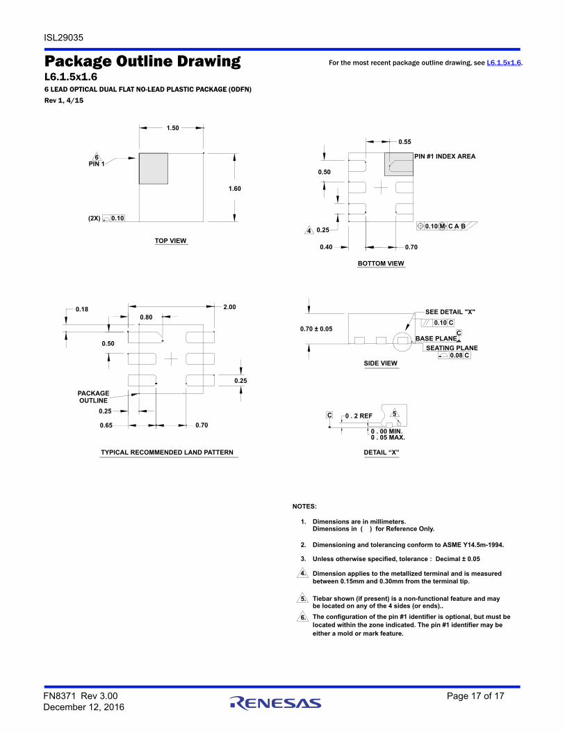
Package Outline DrawingL6.1.5x1.66 LEAD OPTICAL DUAL FLAT NO-LEAD PLASTIC PACKAGE (ODFN)
Rev 1, 4/15
BOTTOM VIEW
SIDE VIEW
TYPICAL RECOMMENDED LAND PATTERN
TOP VIEW
located within the zone indicated. The pin #1 identifier may be
Unless otherwise specified, tolerance : Decimal ± 0.05
The configuration of the pin #1 identifier is optional, but must be
between 0.15mm and 0.30mm from the terminal tip.Dimension applies to the metallized terminal and is measured
Dimensions in ( ) for Reference Only.
Dimensioning and tolerancing conform to ASME Y14.5m-1994.
6.
either a mold or mark feature.
3.
5.
4.
2.
Dimensions are in millimeters.1.
NOTES:
PIN #1 INDEX AREA
C
SEATING PLANE
BASE PLANE
0.08
0.10
SEE DETAIL "X"
C
C
0 . 00 MIN.0 . 05 MAX.
0 . 2 REFC 5
PACKAGE
0.70 ± 0.05
1.50
1.60
PIN 16
(2X) 0.10
0.40
0.25
0.50
0.70
0.55
2.00
0.65
0.25
0.18
0.50
0.80
0.70
0.25
B0.10 M AC
OUTLINE
DETAIL “X”
4
Tiebar shown (if present) is a non-functional feature and maybe located on any of the 4 sides (or ends)..
For the most recent package outline drawing, see L6.1.5x1.6.