Embed Size (px)
Citation preview
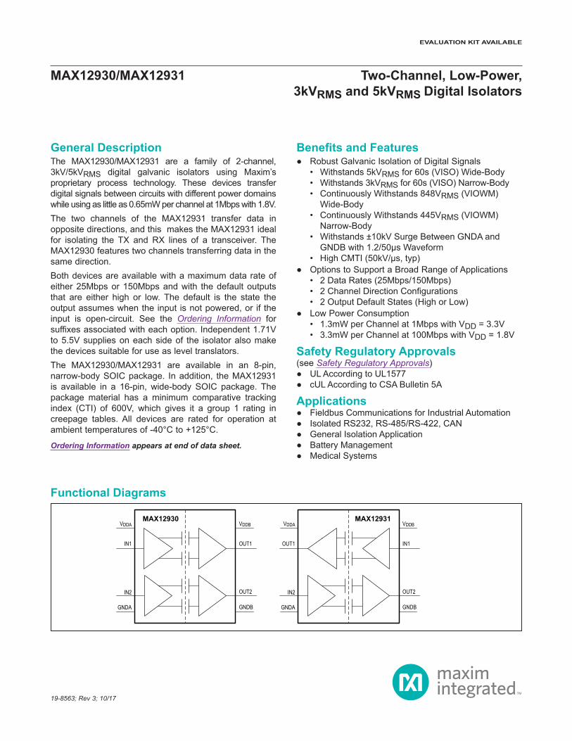
General DescriptionThe MAX12930/MAX12931 are a family of 2-channel, 3kV/5kVRMS digital galvanic isolators using Maxim’s proprietary process technology. These devices transfer digital signals between circuits with different power domains while using as little as 0.65mW per channel at 1Mbps with 1.8V.The two channels of the MAX12931 transfer data in opposite directions, and this makes the MAX12931 ideal for isolating the TX and RX lines of a transceiver. The MAX12930 features two channels transferring data in the same direction. Both devices are available with a maximum data rate of either 25Mbps or 150Mbps and with the default outputs that are either high or low. The default is the state the output assumes when the input is not powered, or if the input is open-circuit. See the Ordering Information for suffixes associated with each option. Independent 1.71V to 5.5V supplies on each side of the isolator also make the devices suitable for use as level translators. The MAX12930/MAX12931 are available in an 8-pin, narrow-body SOIC package. In addition, the MAX12931 is available in a 16-pin, wide-body SOIC package. The package material has a minimum comparative tracking index (CTI) of 600V, which gives it a group 1 rating in creepage tables. All devices are rated for operation at ambient temperatures of -40°C to +125°C.
Benefits and Features Robust Galvanic Isolation of Digital Signals
• Withstands 5kVRMS for 60s (VISO) Wide-Body• Withstands 3kVRMS for 60s (VISO) Narrow-Body• Continuously Withstands 848VRMS (VIOWM)
Wide-Body• Continuously Withstands 445VRMS (VIOWM)
Narrow-Body• Withstands ±10kV Surge Between GNDA and
GNDB with 1.2/50µs Waveform• High CMTI (50kV/µs, typ)
Options to Support a Broad Range of Applications• 2 Data Rates (25Mbps/150Mbps)• 2 Channel Direction Configurations• 2 Output Default States (High or Low)
Low Power Consumption• 1.3mW per Channel at 1Mbps with VDD = 3.3V• 3.3mW per Channel at 100Mbps with VDD = 1.8V
Safety Regulatory Approvals(see Safety Regulatory Approvals)
UL According to UL1577 cUL According to CSA Bulletin 5A
Applications Fieldbus Communications for Industrial Automation Isolated RS232, RS-485/RS-422, CAN General Isolation Application Battery Management Medical Systems
Ordering Information appears at end of data sheet.
19-8563; Rev 3; 10/17
MAX12930/MAX12931 Two-Channel, Low-Power, 3kVRMS and 5kVRMS Digital Isolators
Functional Diagrams
MAX12930VDDA
IN1
IN2
GNDA
VDDB
OUT1
OUT2
GNDB
MAX12931VDDA
OUT1
IN2
GNDA
VDDB
IN1
OUT2
GNDB
EVALUATION KIT AVAILABLE

VDDA to GNDA ........................................................-0.3V to +6VVDDB to GNDB ........................................................-0.3V to +6VIN_ on SIDE A to GNDA ..........................................-0.3V to +6VIN_ on SIDE B to GNDB .........................................-0.3V to +6VOUT_ on SIDE A to GNDA ....................... -0.3V to VDDA + 0.3VOUT_ on SIDE B to GNDB ...................... -0.3V to VDDB + 0.3VShort-Circuit DurationOUT_ on SIDE A to GNDA, OUT_ on SIDE B to GNDB
...............................................................................Continuous
Continuous Power Dissipation (TA = +70°C) Wide SOIC (derate 14.1mW/°C above +70°C) ......1126.8mW Narrow SOIC (derate 5.9mW/°C above +70°C) .......470.6mWOperating Temperature Range ......................... -40°C to +125°CMaximum Junction Temperature .....................................+150°CStorage Temperature Range ............................ -60°C to +150°CSoldering Temperature (reflow) .......................................+260°C
Wide SOIC Junction-to-Ambient Thermal Resistance (θJA) ..........71°C/W Junction-to-Case Thermal Resistance (θJC) ...............23°C/W
Narrow SOIC Junction-to-Ambient Thermal Resistance (θJA) ........170°C/W Junction-to-Case Thermal Resistance (θJC) ...............38°C/W
(Note 1)
(VDDA - VGNDA = 1.71V to 5.5V, VDDB - VGNDB = 1.71V to 5.5V, CL = 15pF, TA = -40°C to +125°C, unless otherwise noted. Typical values are at VDDA - VGNDA = 3.3V, VDDB - VGNDB = 3.3V, GNDA = GNDB, TA = 25°C, unless otherwise noted.) (Note 2)
MAX12930/MAX12931 Two-Channel, Low-Power, 3kVRMS and 5kVRMS Digital Isolators
www.maximintegrated.com Maxim Integrated 2
Note 1: Package thermal resistances were obtained using the method described in JEDEC specification JESD51-7, using a four-layer board. For detailed information on package thermal considerations, refer to www.maximintegrated.com/thermal-tutorial.
Absolute Maximum Ratings
Stresses beyond those listed under “Absolute Maximum Ratings” may cause permanent damage to the device. These are stress ratings only, and functional operation of the device at these or any other conditions beyond those indicated in the operational sections of the specifications is not implied. Exposure to absolute maximum rating conditions for extended periods may affect device reliability.
Package Thermal Characteristics
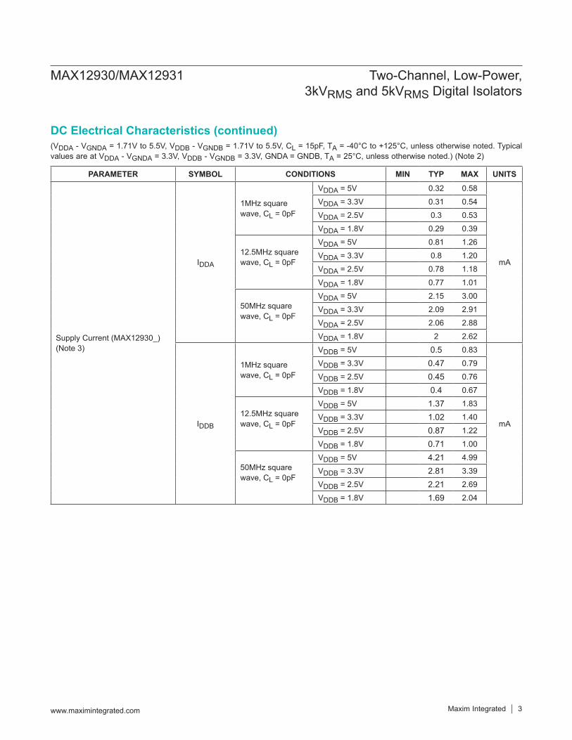
DC Electrical Characteristics
PARAMETER SYMBOL CONDITIONS MIN TYP MAX UNITS
POWER SUPPLY
Supply VoltageVDDA Relative to GNDA 1.71 5.5
VVDDB Relative to GNDB 1.71 5.5
Undervoltage-Lockout Threshold VUVLO_ VDD_ rising 1.5 1.6 1.66 V
Undervoltage-Lockout Threshold Hysteresis VUVLO_HYST 45 mV
(VDDA - VGNDA = 1.71V to 5.5V, VDDB - VGNDB = 1.71V to 5.5V, CL = 15pF, TA = -40°C to +125°C, unless otherwise noted. Typical values are at VDDA - VGNDA = 3.3V, VDDB - VGNDB = 3.3V, GNDA = GNDB, TA = 25°C, unless otherwise noted.) (Note 2)
MAX12930/MAX12931 Two-Channel, Low-Power, 3kVRMS and 5kVRMS Digital Isolators
www.maximintegrated.com Maxim Integrated 3
DC Electrical Characteristics (continued)
PARAMETER SYMBOL CONDITIONS MIN TYP MAX UNITS
Supply Current (MAX12930_)(Note 3)
IDDA
1MHz square wave, CL = 0pF
VDDA = 5V 0.32 0.58
mA
VDDA = 3.3V 0.31 0.54
VDDA = 2.5V 0.3 0.53
VDDA = 1.8V 0.29 0.39
12.5MHz square wave, CL = 0pF
VDDA = 5V 0.81 1.26
VDDA = 3.3V 0.8 1.20
VDDA = 2.5V 0.78 1.18
VDDA = 1.8V 0.77 1.01
50MHz square wave, CL = 0pF
VDDA = 5V 2.15 3.00
VDDA = 3.3V 2.09 2.91
VDDA = 2.5V 2.06 2.88
VDDA = 1.8V 2 2.62
IDDB
1MHz square wave, CL = 0pF
VDDB = 5V 0.5 0.83
mA
VDDB = 3.3V 0.47 0.79
VDDB = 2.5V 0.45 0.76
VDDB = 1.8V 0.4 0.67
12.5MHz square wave, CL = 0pF
VDDB = 5V 1.37 1.83
VDDB = 3.3V 1.02 1.40
VDDB = 2.5V 0.87 1.22
VDDB = 1.8V 0.71 1.00
50MHz square wave, CL = 0pF
VDDB = 5V 4.21 4.99
VDDB = 3.3V 2.81 3.39
VDDB = 2.5V 2.21 2.69
VDDB = 1.8V 1.69 2.04

(VDDA - VGNDA = 1.71V to 5.5V, VDDB - VGNDB = 1.71V to 5.5V, CL = 15pF, TA = -40°C to +125°C, unless otherwise noted. Typical values are at VDDA - VGNDA = 3.3V, VDDB - VGNDB = 3.3V, GNDA = GNDB, TA = 25°C, unless otherwise noted.) (Note 2)
MAX12930/MAX12931 Two-Channel, Low-Power, 3kVRMS and 5kVRMS Digital Isolators
www.maximintegrated.com Maxim Integrated 4
DC Electrical Characteristics (continued)
PARAMETER SYMBOL CONDITIONS MIN TYP MAX UNITS
Supply Current (MAX12931_)(Note 3)
IDDA
1MHz square wave, CL = 0pF
VDDA = 5V 0.42 0.70
mA
VDDA = 3.3V 0.39 0.67
VDDA = 2.5V 0.38 0.64
VDDA = 1.8V 0.36 0.56
12.5MHz square wave, CL = 0pF
VDDA = 5V 1.07 1.52
VDDA = 3.3V 0.89 1.29
VDDA = 2.5V 0.81 1.19
VDDA = 1.8V 0.73 1.03
50MHz square wave, CL = 0pF
VDDA = 5V 3.06 3.87
VDDA = 3.3V 2.37 3.06
VDDA = 2.5V 2.08 2.72
VDDA = 1.8V 1.82 2.33
IDDB
1MHz square wave, CL = 0pF
VDDB = 5V 0.42 0.70
mA
VDDB = 3.3V 0.39 0.67
VDDB = 2.5V 0.38 0.64
VDDB = 1.8V 0.36 0.56
12.5MHz square wave, CL = 0pF
VDDB = 5V 1.07 1.52
VDDB = 3.3V 0.89 1.29
VDDB = 2.5V 0.81 1.19
VDDB = 1.8V 0.73 1.03
50MHz square wave, CL = 0pF
VDDB = 5V 3.06 3.87
VDDB = 3.3V 2.37 3.06
VDDB = 2.5V 2.08 2.72
VDDB = 1.8V 1.82 2.33LOGIC INPUTS AND OUTPUTS
Input High Voltage VIH 2.25V ≤ VDD_ ≤ 5.5V 0.7 x VDD_ V 1.71V ≤ VDD_ < 2.25V 0.75 x VDD_
Input Low Voltage VIL2.25V ≤ VDD_ ≤ 5.5V 0.8
V1.71V ≤ VDD_ < 2.25V 0.7
Input Hysteresis VHYSMAX1293_B/E 410
mVMAX1293_C/F 80
Input Pullup Current (Note 4) IPU IN_, MAX1293_B/C -10 -5 -1.5 µA
Input Pulldown Current (Note 4) IPD IN_, MAX1293_E/F 1.5 5 10 µA
Input Capacitance CIN IN_, fSW = 1MHz 2 pF

(VDDA - VGNDA = 1.71V to 5.5V, VDDB - VGNDB = 1.71V to 5.5V, CL = 15pF, TA = -40°C to +125°C, unless otherwise noted. Typical values are at VDDA - VGNDA = 3.3V, VDDB - VGNDB = 3.3V, GNDA = GNDB, TA = 25°C, unless otherwise noted.) (Note 2)
(VDDA - VGNDA = 1.71V to 5.5V, VDDB - VGNDB = 1.71V to 5.5V, CL = 15pF, TA = -40°C to +125°C, unless otherwise noted. Typical values are at VDDA - VGNDA = 3.3V, VDDB - VGNDB = 3.3V, GNDA = GNDB, TA = 25°C, unless otherwise noted.) (Notes 2,3)
MAX12930/MAX12931 Two-Channel, Low-Power, 3kVRMS and 5kVRMS Digital Isolators
www.maximintegrated.com Maxim Integrated 5
DC Electrical Characteristics (continued)
PARAMETER SYMBOL CONDITIONS MIN TYP MAX UNITS
Output Voltage High (Note 4) VOH IOUT = 4mA source VDD_ - 0.4 V
Output Voltage Low (Note 4) VOL IOUT = 4mA sink 0.4 V
Dynamic Characteristics MAX1293_B/E
PARAMETER SYMBOL CONDITIONS MIN TYP MAX UNITS
Common-Mode Transient Im-munity CMTI IN_ = GND_ or VDD_ (Note 5) 50 kV/µs
Maximum Data Rate DRMAX 25 Mbps
Minimum Pulse Width PWMIN 40 ns
Glitch Rejection 10 17 29 ns
Propagation Delay (Figure 1)
tPLH
4.5V ≤ VDD_ ≤ 5.5V 17.4 23.9 32.5
ns
3.0V ≤ VDD_ ≤ 3.6V 17.6 24.4 33.7
2.25V ≤ VDD_ ≤ 2.75V 18.3 25.8 36.7
1.71V ≤ VDD_ ≤ 1.89V 20.7 29.6 43.5
tPHL
4.5V ≤ VDD_ ≤ 5.5V 16.9 23.4 33.6
3.0V ≤ VDD_ ≤ 3.6V 17.2 24.2 35.1
2.25V ≤ VDD_ ≤ 2.75V 17.8 25.4 38.2
1.71V ≤ VDD_ ≤ 1.89V 19.8 29.3 45.8
Pulse Width Distortion PWD 0.4 4 ns
Propagation Delay Skew Part-to-Part (same channel)
tSPLH
4.5V ≤ VDD_ ≤ 5.5V 15.1
ns
3.0V ≤ VDD_ ≤ 3.6V 15
2.25V ≤ VDD_ ≤ 2.75V 15.4
1.71V ≤ VDD_ ≤ 1.89V 20.5
tSPHL
4.5V ≤ VDD_ ≤ 5.5V 13.9
3.0V ≤ VDD_ ≤ 3.6V 14.2
2.25V ≤ VDD_ ≤ 2.75V 16
1.71V ≤ VDD_ ≤ 1.89V 21.8
Propagation Delay Skew Chan-nel-to-Channel (Same Direction) MAX12930 only
tSCSLH 2ns
tSCSHL 2

(VDDA - VGNDA = 1.71V to 5.5V, VDDB - VGNDB = 1.71V to 5.5V, CL = 15pF, TA = -40°C to +125°C, unless otherwise noted. Typical values are at VDDA - VGNDA = 3.3V, VDDB - VGNDB = 3.3V, GNDA = GNDB, TA = 25°C, unless otherwise noted.) (Notes 2,3)
MAX12930/MAX12931 Two-Channel, Low-Power, 3kVRMS and 5kVRMS Digital Isolators
www.maximintegrated.com Maxim Integrated 6
Dynamic Characteristics MAX1293_B/E (continued)
PARAMETER SYMBOL CONDITIONS MIN TYP MAX UNITSPropagation Delay Skew Channel-to-Channel (Opposite Direction)MAX12931 Only
tSCOLH 2ns
tSCOHL 2
Peak Eye Diagram Jitter TJIT(PK) 25Mbps 250 ps
Rise Time tR
4.5V ≤ VDD_ ≤ 5.5V 1.6
ns3.0V ≤ VDD_ ≤ 3.6V 2.2
2.25V ≤ VDD_ ≤ 2.75V 3
1.71V ≤ VDD_ ≤ 1.89V 4.5
Fall Time tF
4.5V ≤ VDD_ ≤ 5.5V 1.4
ns3.0V ≤ VDD_ ≤ 3.6V 2
2.25V ≤ VDD_ ≤ 2.75V 2.8
1.71V ≤ VDD_ ≤ 1.89V 5.1

(VDDA - VGNDA = 1.71V to 5.5V, VDDB - VGNDB = 1.71V to 5.5V, CL = 15pF, TA = -40°C to +125°C, unless otherwise noted. Typical values are at VDDA - VGNDA = 3.3V, VDDB - VGNDB = 3.3V, GNDA = GNDB, TA = 25°C, unless otherwise noted.) (Notes 2,3)
MAX12930/MAX12931 Two-Channel, Low-Power, 3kVRMS and 5kVRMS Digital Isolators
www.maximintegrated.com Maxim Integrated 7
Dynamic Characteristics MAX1293_C/F
PARAMETER SYMBOL CONDITIONS MIN TYP MAX UNITS
Common-Mode Transient Immunity CMTI IN_ = GND_ or VDD_ (Note 5) 50 kV/us
Maximum Data Rate DRMAX 150 Mbps
Minimum Pulse Width PWMIN2.25V ≤ VDD_ ≤ 5.5V 5
ns1.71V ≤ VDD_ ≤ 1.89V 6.67
Propagation Delay (Figure 1)
tPLH
4.5V ≤ VDD_ ≤ 5.5V 4.1 5.4 9.2
ns
3.0V ≤ VDD_ ≤ 3.6V 4.2 5.9 10.2
2.25V ≤ VDD_ ≤ 2.75V 4.9 7.1 13.4
1.71V ≤ VDD_ ≤ 1.89V 7.1 10.9 20.3
tPHL
4.5V ≤ VDD_ ≤ 5.5V 4.3 5.6 9.4
3.0V ≤ VDD_ ≤ 3.6V 4.4 6.2 10.5
2.25V ≤ VDD_ ≤ 2.75V 5.1 7.3 14.1
1.71V ≤ VDD_ ≤ 1.89V 7.2 10.9 21.7
Pulse Width Distortion PWD 0.3 2 ns
Propagation Delay Skew Part-to-Part (Same Channel)
tSPLH
4.5V ≤ VDD_ ≤ 5.5V 3.7
ns
3.0V ≤ VDD_ ≤ 3.6V 4.3
2.25V ≤ VDD_ ≤ 2.75V 6
1.71V ≤ VDD_ ≤ 1.89V 10.3
tSPHL
4.5V ≤ VDD_ ≤ 5.5V 3.8
3.0V ≤ VDD_ ≤ 3.6V 4.7
2.25V ≤ VDD_ ≤ 2.75V 6.5
1.71V ≤ VDD_ ≤ 1.89V 11.5Propagation Delay Skew Channel-to-Channel (Same Direction) MAX12930 Only
tSCSLH 2ns
tSCSHL 2
Propagation Delay Skew Channel-to-Channel (Opposite Direction) MAX12931 Only
tSCOLH 2ns
tSCOHL 2
Peak Eye Diagram Jitter TJIT(PK) 150Mbps 90 ps
Clock Jitter RMS TJCLK(RMS)500kHz Clock Input Rising/Falling Edges 6.5 ps

(VDDA - VGNDA = 1.71V to 5.5V, VDDB - VGNDB = 1.71V to 5.5V, CL = 15pF, TA = -40°C to +125°C, unless otherwise noted. Typical values are at VDDA - VGNDA = 3.3V, VDDB - VGNDB = 3.3V, GNDA = GNDB, TA = 25°C, unless otherwise noted.) (Notes 2,3)
Note 2: All devices are 100% production tested at TA = +25°C. Specifications over temperature are guaranteed by design.Note 3: Not production tested. Guaranteed by design and characterization.Note 4: All currents into the device are positive. All currents out of the device are negative. All voltages are referenced to their
respective ground (GNDA or GNDB), unless otherwise noted.Note 5: CMTI is the maximum sustainable common-mode voltage slew rate while maintaining the correct output. CMTI applies to
both rising and falling common-mode voltage sedges. Tested with the transient generator connected between GNDA and GNDB (VCM = 1000V).
MAX12930/MAX12931 Two-Channel, Low-Power, 3kVRMS and 5kVRMS Digital Isolators
www.maximintegrated.com Maxim Integrated 8
ESD Protection
Dynamic Characteristics MAX1293_C/F (continued)
PARAMETER SYMBOL CONDITIONS MIN TYP MAX UNITS
Rise Time tR
4.5V ≤ VDD_ ≤ 5.5V 1.6
ns3.0V ≤ VDD_ ≤ 3.6V 2.2
2.25V ≤ VDD_ ≤ 2.75V 3
1.71V ≤ VDD_ ≤ 1.89V 4.5
Fall Time tF
4.5V ≤ VDD_ ≤ 5.5V 1.4
ns3.0V ≤ VDD_ ≤ 3.6V 2
2.25V ≤ VDD_ ≤ 2.75V 2.8
1.71V ≤ VDD_ ≤ 1.89V 5.1
PARAMETER SYMBOL CONDITIONS MIN TYP MAX UNITS
ESD Human Body Model, all pins ±3 kV
Safety Regulatory ApprovalsULThe MAX12930–MAX12931 narrow-body SOIC are certified under UL1577. For more details, refer to file E351759.
Rated up to 3000VRMS isolation voltage for single protection.
cUL (Equivalent to CSA Notice 5A)The MAX12930–MAX12931 narrow-body SOIC are certified up to 3000VRMS for single protection. For more details, refer to file E351759.
ULThe MAX12931 wide-body SOIC is certified under UL1577. For more details, refer to file E351759.
Rated up to 5000VRMS isolation voltage for single protection.
cUL (Equivalent to CSA notice 5A)The MAX12931 wide-body SOIC is certified up to 5000VRMS for single protection. For more details, refer to file E351759.

Table 1. Narrow SOIC Insulation Characteristic
MAX12930/MAX12931 Two-Channel, Low-Power, 3kVRMS and 5kVRMS Digital Isolators
www.maximintegrated.com Maxim Integrated 9
Insulation Characteristics
PARAMETER SYMBOL CONDITIONS VALUE UNITS
Partial Discharge Test Voltage VPRMethod B1 = VIORM x 1.875 (t = 1s, partial discharge < 5pC) 1182 VP
Maximum Repetitive Peak Isolation Voltage VIORM (Note 6) 630 VP
Maximum Working Isolation Voltage VIOWM
Continuous RMS voltage(Note 6) 445 VRMS
Maximum Transient Isolation Voltage VIOTM t = 1s 6000 VP
Maximum Withstand Isolation Voltage VISO fSW = 60Hz, duration = 60s (Note 7) 3000 VRMS
Maximum Surge Isolation Voltage VIOSMBasic Insulation, 1.2/50µs pulse per IEC61000-4-5 10 kV
Insulation Resistance RS TA = 150°C, VIO = 500V >109 Ω
Barrier Capacitance Side A to Side B CIO fSW = 1MHz (Note 8) 2 pF
Minimum Creepage Distance CPG Narrow SOIC 4 mm
Minimum Clearance Distance CLR Narrow SOIC 4 mm
Internal Clearance Distance through insulation 0.015 mm
Comparative Tracking Index CTI Material Group I (IEC60112) >600
Climate Category 40/125/21
Pollution Degree (DIN VDE 0110, Table 1) 2

Note 6: VISO, VIOWM and VIORM are defined by the IEC 60747-5-5 standard.Note 7: Product is qualified at VISO for 60s and 100% production tested at 120% of VISO for 1s.Note 8: Capacitance is measured with all pins on side A and side B tied together.
Table 2. Wide SOIC Insulation Characteristic
MAX12930/MAX12931 Two-Channel, Low-Power, 3kVRMS and 5kVRMS Digital Isolators
www.maximintegrated.com Maxim Integrated 10
PARAMETER SYMBOL CONDITIONS VALUE UNITS
Partial Discharge Test Voltage VPRMethod B1 = VIORM x 1.875 (t = 1s, partial discharge < 5pC) 2250 VP
Maximum Repetitive Peak Isolation Voltage VIORM (Note 6) 1200 VP
Maximum Working Isolation Voltage VIOWM
Continuous RMS voltage(Note 6) 848 VRMS
Maximum Transient Isolation Voltage VIOTM t = 1s 8400 VP
Maximum Withstand Isolation Voltage VISO fSW = 60Hz, duration = 60s (Note 7) 5000 VRMS
Maximum Surge Isolation Voltage VIOSMBasic Insulation, 1.2/50µs pulse per IEC61000-4-5 10 kV
Insulation Resistance RS TA = 150°C, VIO = 500V >109 Ω
Barrier Capacitance Side A to Side B CIO fSW = 1MHz (Note 8) 2 pF
Minimum Creepage Distance CPG Wide SOIC 8 mm
Minimum Clearance Distance CLR Wide SOIC 8 mm
Internal Clearance Distance through insulation 0.015 mm
Comparative Tracking Index CTI Material Group I (IEC60112) >600
Climate Category 40/125/21
Pollution Degree (DIN VDE 0110, Table 1) 2

(VVDDA - VGNDA = +3.3V, VVDDB - VGNDB = +3.3V, VGNDA = VGNDB, TA = +25°C, unless otherwise noted.)
Figure 1. Test Circuit (A) and Timing Diagram (B)
MAX12930/MAX12931 Two-Channel, Low-Power, 3kVRMS and 5kVRMS Digital Isolators
www.maximintegrated.com Maxim Integrated 11
MAX12930MAX12931
Typical Operating Characteristics
0.0
0.2
0.4
0.6
0.8
1.0
0 5 10 15 20 25
SUPP
LYCU
RREN
T(m
A)
DATA RATE (Mbps)
SIDE A SUPPLY CURRENTvs. DATA RATE
DRIVING ONE CHANNEL ON SIDE AOTHER CHANNEL IS HIGHMAX12930B/E
toc01
VDDA = 5.0VVDDA = 3.3VVDDA = 2.5VVDDA = 1.8V
0.0
0.5
1.0
1.5
2.0
2.5
0 25 50 75 100 125 150
SUPP
LYCU
RREN
T(m
A)
DATA RATE (Mbps)
SIDE A SUPPLY CURRENTvs. DATA RATE
DRIVING ONE CHANNEL ON SIDE AOTHER CHANNEL IS HIGHMAX12930C/F
toc02
VDDA = 5.0VVDDA = 3.3VVDDA = 2.5VVDDA = 1.8V
0.0
0.2
0.4
0.6
0.8
1.0
0 5 10 15 20 25
SUPP
LYCU
RREN
T(m
A)
DATA RATE (Mbps)
SIDE A SUPPLY CURRENTvs. DATA RATE
DRIVING ONE CHANNEL ON SIDE AOTHER CHANNEL IS HIGHMAX12931B/E
toc03
VDDA = 5.0VVDDA = 3.3VVDDA = 2.5VVDDA = 1.8V

(VVDDA - VGNDA = +3.3V, VVDDB - VGNDB = +3.3V, VGNDA = VGNDB, TA = +25°C, unless otherwise noted.)
MAX12930/MAX12931 Two-Channel, Low-Power, 3kVRMS and 5kVRMS Digital Isolators
Maxim Integrated 12www.maximintegrated.com
Typical Operating Characteristics (continued)
0.0
0.5
1.0
1.5
2.0
2.5
0 25 50 75 100 125 150
SUPP
LYCU
RREN
T(m
A)
DATA RATE (Mbps)
SIDE A SUPPLY CURRENTvs. DATA RATE
DRIVING ONE CHANNEL ON SIDE AOTHER CHANNEL IS HIGHMAX12931C/F
toc04
VDDA = 5.0VVDDA = 3.3VVDDA = 2.5VVDDA = 1.8V
0.0
0.2
0.4
0.6
0.8
1.0
0 5 10 15 20 25
SUPP
LYCU
RREN
T(m
A)
DATA RATE (Mbps)
DRIVING ONE CHANNEL ON SIDE ACL = 0pF, OTHER CHANNEL IS HIGH,MAX12930B/E
toc05
VDDB = 5.0VVDDB = 3.3VVDDB = 2.5VVDDB = 1.8V
0.0
0.2
0.4
0.6
0.8
1.0
1.2
1.4
1.6
0 5 10 15 20 25
SUPP
LYCU
RREN
T(m
A)
DATA RATE (Mbps)
DRIVING ONE CHANNEL ON SIDE ACL = 15pF, OTHER CHANNEL IS HIGH,MAX12930B/E
toc06
VDDB = 5.0VVDDB = 3.3VVDDB = 2.5VVDDB = 1.8V
0.0
0.5
1.0
1.5
2.0
2.5
3.0
3.5
0 25 50 75 100 125 150
SUPP
LYCU
RREN
T(m
A)
DATA RATE (Mbps)
DRIVING ONE CHANNEL ON SIDE ACL= 0pF, OTHER CHANNEL IS HIGH,MAX12930C/F
toc07
VDDB = 5.0VVDDB = 3.3VVDDB = 2.5VVDDB = 1.8V
0.000
0.500
1.000
1.500
2.000
2.500
0 5 10 15 20 25
SUPP
LYCU
RREN
T(m
A)
DATA RATE (Mbps)
DRIVING ONE CHANNEL ON SIDE ACL = 15pF, OTHER CHANNEL IS HIGHMAX12931B/E
toc10
VDDB = 5.0VVDDB = 3.3VVDDB = 2.5VVDDB = 1.8V
0.0
1.0
2.0
3.0
4.0
5.0
6.0
7.0
8.0
0 25 50 75 100 125 150
SUPP
LYCU
RREN
T(m
A)
DATA RATE (Mbps)
DRIVING ONE CHANNEL ON SIDE ACL = 15pF, OTHER CHANNEL IS HIGH,MAX12930C/F
toc08
VDDB = 5.0VVDDB = 3.3VVDDB = 2.5VVDDB = 1.8V
0.0
0.5
1.0
1.5
2.0
2.5
3.0
0 25 50 75 100 125 150
SUPP
LYCU
RREN
T(m
A)
DATA RATE (Mbps)
DRIVING ONE CHANNEL ON SIDE ACL = 0pF, OTHER CHANNEL IS HIGHMAX12931C/F
toc11
VDDB = 5.0VVDDB = 3.3VVDDB = 2.5VVDDB = 1.8V
0.0
0.2
0.4
0.6
0.8
1.0
0 5 10 15 20 25
SUPP
LYCU
RREN
T(m
A)
DATA RATE (Mbps)
DRIVING ONE CHANNEL ON SIDE AC = 0pF, OTHER CHANNEL IS HIGHLMAX12931B/E
toc09
VDDB = 5.0VVDDB = 3.3VVDDB = 2.5VVDDB = 1.8V
0.0
1.0
2.0
3.0
4.0
5.0
6.0
7.0
8.0
0 25 50 75 100 125 150
SUPP
LYCU
RREN
T(m
A)
DATA RATE (Mbps)
DRIVING ONE CHANNEL ON SIDE ACL = 15pF, OTHER CHANNEL IS HIGHMAX12931C/F
toc12
VDDB = 5.0VVDDB = 3.3VVDDB = 2.5VVDDB = 1.8V

MAX12930/MAX12931 Two-Channel, Low-Power, 3kVRMS and 5kVRMS Digital Isolators
Maxim Integrated 13www.maximintegrated.com
(VVDDA - VGNDA = +3.3V, VVDDB - VGNDB = +3.3V, VGNDA = VGNDB, TA = +25°C, unless otherwise noted.)Typical Operating Characteristics (continued)
0.0
3.0
6.0
9.0
12.0
15.0
-50 -25 0 25 50 75 100 125
PROP
AGAT
ION
DELA
Y(n
s)
TEMPERATURE (°C)
PROPAGATION DELAYvs. TEMPERATURE
VDDA = VDDBINA TO OUTBMAX1293_C/F
toc13
VDDA = 1.8VVDDA = 2.5VVDDA = 3.3VVDDA = 5.5V
15
20
25
30
35
-50 -25 0 25 50 75 100 125
PROP
AGAT
ION
DELA
Y(n
s)
TEMPERATURE (°C)
PROPAGATION DELAYvs. TEMPERATURE
VDDA= VDDBINA TO OUTB,MAX1293_B/E
toc14
VDDA = 1.8VVDDA = 2.5VVDDA = 3.3VVDDA = 5.5V
0.0
5.0
10.0
15.0
20.0
25.0
30.0
35.0
1.5 2.5 3.5 4.5 5.5
PROP
AGAT
ION
DELA
Y(n
s)
VDDAVOLTAGE (V)
PROPAGATION DELAYvs. VDDAVOLTAGE
VDDB = 3.3VINA TO OUTB
toc15
MAX1293_B/E
MAX1293_C/F
0.0
5.0
10.0
15.0
20.0
25.0
30.0
35.0
1.5 2.5 3.5 4.5 5.5
PROP
AGAT
ION
DELA
Y(n
s)
VDDBVOLTAGE (V)
PROPAGATION DELAYvs. VDDB VOLTAGE
VDDA= 3.3VINA TO OUTB
toc16
MAX1293_C/F
MAX1293_B/E
toc17
5ns/div
1V/div
MAX1293_C/F
IN__
OUT__
1V/div
5ns pulse
toc19
400mV/div
EYE DIAGRAM at 150MbpsMAX12931C/F
1ns/div
toc18
20ns/div
MINIMUM PULSE WIDTH
1V/div
MAX1293_B/E40ns pulse
IN__
OUT__
1V/div
400mV/div
toc20
125ps/div
CLOCK JITTER RMS ON RISING EDGEMAX1293_C/F
500kHz Clock InputtJCLK(RMS) = 6.3ps
OUT_ 400mV/div
toc21
125ps/div
CLOCK JITTER RMS ON FALLING EDGEMAX1293_C/F
OUT_
500kHz Clock InputtJCLK(RMS) = 6.5ps

MAX12930/MAX12931 Two-Channel, Low-Power, 3kVRMS and 5kVRMS Digital Isolators
www.maximintegrated.com Maxim Integrated 14
Pin Configurations
VDDB
OUT1
OUT2
GNDB
8
7
6
5
1
2
3
4
VDDA
IN1
IN2
GNDA
MAX12930
NARROW SOIC
TOP VIEW
+VDDB
IN1
OUT2
GNDB
8
7
6
5
1
2
3
4
VDDA
OUT1
IN2
GNDA
MAX12931
NARROW SOIC
+
MAX12931
+
WIDE SOIC
N.C.2N.C.
GNDB1GNDA
IN14OUT1
VDDB3VDDA
N.C.6N.C.
OUT25IN2
GNDB98N.C.
N.C.107GNDA
11
12
13
14
15
16

MAX12930/MAX12931 Two-Channel, Low-Power, 3kVRMS and 5kVRMS Digital Isolators
www.maximintegrated.com Maxim Integrated 15
Pin DescriptionPIN
NAME FUNCTION REFERENCEMAX12930 8-PIN SOIC
MAX129318-PIN SOIC
MAX12931 16-PIN SOIC
1 1 3 VDDAPower Supply for side A. Bypass VDDA with a 0.1µF ceramic capacitor to GNDA. GNDA
2 — — IN1 Logic input for channel 1 GNDA
— 2 4 OUT1 Logic output of channel 1 GNDA
3 3 5 IN2 Logic input for channel 2 GNDA
4 4 1, 7 GNDA Ground reference for side A —
5 5 9, 16 GNDB Ground reference for side B —
6 6 12 OUT2 Logic output of channel 2 GNDB
7 — — OUT1 Logic output of channel 1 GNDB
— 7 13 IN1 Logic input for channel 1 GNDB
8 8 14 VDDBPower Supply for side B. Bypass VDDB with a 0.1µF ceramic capacitor to GNDB. GNDB
— — 2, 6, 8, 10, 11, 15 N.C. Not internally connected —
Typical Operating Circuit
MAX12931VDDA
OUT1
IN2
GNDA
VDDB
IN1
OUT2
GNDB
0.1µF
2.5V
MICROCONTROLLER
0.1µF
3.3V
VDD
RXDA
B
TRANSCEIVER
Y
Z
TXD
GND
VDD
RX
TX
GND

Detailed DescriptionThe MAX12930/MAX12931 are a family of 2-channel digital isolators. The MAX12930 transfers digital signals between circuits with different power domain in one direction, which is convenient for applications such as digital I/O. The MAX12931 transfers digital signals in opposite directions, which is necessary for isolated RS-485 or other UART applications.Devices available in the 8-pin narrow body SOIC package are rated for up to 3kVRMS isolation voltage for 60 seconds and the device in the 16-pin wide body SOIC package is rated for up to 5kVRMS. This family of digital isolators offers low-power operation, high electromagnetic interference (EMI) immunity, and stable temperature performance through Maxim’s proprietary process technology. The devices isolate different ground domains and block high-voltage/high-current transients from sensitive or human interface circuitry.Devices are available with data rates from DC to 25Mbps (B/E versions) or 150Mbps (C/F versions). Each device can be ordered with default-high or default-low outputs. The default is the state the output assumes when the input is not powered, or if the input is open circuit.The devices have two supply inputs (VDDA and VDDB) that independently set the logic levels on either side of device. VDDA and VDDB are referenced to GNDA and GNDB, respectively. The MAX12930/MAX12931 family also features a refresh circuit to ensure output accuracy when an input remains in the same state indefinitely.
Digital IsolationThe device family provides galvanic isolation for digital signals that are transmitted between two ground domains. Up to 630VPEAK of continuous isolation is supported
in the narrow SOIC package and up to 1200VPEAK of continuous isolation is supported in the wide SOIC pack-age. The devices withstand differences of up to 3kVRMS in the 8-pin narrow SOIC package or 5kVRMS in the 16-pin wide SOIC package for up to 60 seconds.
Level-ShiftingThe wide supply voltage range of both VDDA and VDDB allows the MAX12930/MAX12931 family to be used for level translation in addition to isolation. VDDA and VDDB can be independently set to any voltage from 1.71V to 5.5V. The supply voltage sets the logic level on the corresponding side of the isolator.
Unidirectional ChannelsEach channel of the MAX12930/MAX12931 is unidirectional; it only passes data in one direction, as indicated in the functional diagram. Each device features two unidirectional channels that operate independently with guaranteed data rates from DC up to 25Mbps (B/E versions), or DC to 150Mbps (C/F versions). The output driver of each channel is push-pull, eliminating the need for pullup resistors. The outputs are able to drive both TTL and CMOS logic inputs.
Startup and Undervoltage-LockoutThe VDDA and VDDB supplies are both internally monitored for undervoltage conditions. Undervoltage events can occur during power-up, power-down, or during normal operation due to a sagging supply voltage. When an undervoltage condition is detected on either supply, all outputs go to their default states regardless of the state of the inputs (Table 3). Figure 2 through Figure 5 show the behavior of the outputs during power-up and power-down.
Table 3. Output Behavior During Undervoltage Conditions
MAX12930/MAX12931 Two-Channel, Low-Power, 3kVRMS and 5kVRMS Digital Isolators
www.maximintegrated.com Maxim Integrated 16
VIN_ VVDDA VVDDB VOUTA_ VOUTB_
1 Powered Powered 1 1
0 Powered Powered 0 0
X Undervoltage Powered Default Default
X Powered Undervoltage Default Default

Figure 2. Undervoltage Lockout Behavior (MAX1293_B/C High)
Figure 4. Undervoltage Lockout Behavior (MAX1293_E/F High)
Figure 3. Undervoltage Lockout Behavior (MAX1293_B/C Low)
Figure 5. Undervoltage Lockout Behavior (MAX1293_E/F Low)
MAX12930/MAX12931 Two-Channel, Low-Power, 3kVRMS and 5kVRMS Digital Isolators
www.maximintegrated.com Maxim Integrated 17
2V/div
200µs/div
VDDA
VDDB
OUT_A
OUT_B
MAX1293_B/CINPUT SET TO HIGH
2V/div
200µs/div
VDDA
VDDB
OUT_A
OUT_B
MAX1293_E/FINPUT SET TO HIGH
2V/div
200µs/div
VDDA
VDDB
OUT_A
OUT_B
MAX1293_B/CINPUT SET TO LOW
2V/div
200µs/div
VDDA
VDDB
OUT_A
OUT_B
MAX1293_E/FINPUT SET TO LOW

Application InformationPower-Supply SequencingThe MAX12930/MAX12931 do not require special power supply sequencing. The logic levels are set independently on either side by VDDA and VDDB. Each supply can be present over the entire specified range regardless of the level or presence of the other supply.
Power-Supply DecouplingTo reduce ripple and the chance of introducing data errors, bypass VDDA and VDDB with 0.1µF low-ESR ceramic capacitors to GNDA and GNDB, respectively. Place the bypass capacitors as close to the power supply input pins as possible.
Layout ConsiderationsThe PCB designer should follow some critical recommendation in order to get the best performance from the design.
Keep the input/output traces as short as possible. Avoid using vias to make low-inductance paths for the signals.
Have a solid ground plane underneath the high-speed signal layer.
Keep the area underneath the MAX12930/MAX12931 free from ground and signal planes. Any galvanic or metallic connection between the field-side and logic-side defeats the isolation.
Calculating Power DissipationThe required current for a given supply (VDDA or VDDB) can be estimated by summing the current required for each channel. The supply current for a channel depends on whether the channel is an input or an output, the channel’s data rate, and the capacitive or resistive load if it is an output. The typical current for an input or output at any data rate can be estimated from the graphs in Figure 6 and Figure 7. Please note that the data in Figure 6 and Figure 7 are extrapolated from the supply current measurements in a typical operating condition.The total current for a single channel is the sum of the “no load” current (shown in Figure 6 and Figure 7) which is a function of Voltage and Data Rate, and the “load current” which depends upon the type of load. Current into a capacitive load is a function of the load capacitance, the switching frequency, and the supply voltage.
ICL = CL × fSW × VDDwhere
ICL is the current required to drive the capacitive load. CL is the load capacitance on the isolator’s output pin.fSW is the switching frequency (bits per second/2).VDD is the supply voltage on the output side of the isolator.Current into a resistive load depends on the load resistance, the supply voltage and the average duty cycle of the data waveform. The DC load current can be conservatively estimated by assuming the output is always high.
IRL = VDD ÷ RLwhereIRL is the current required to drive the resistive load.VDD is the supply voltage on the output side of the isolator. RL is the load resistance on the isolator’s output pin.Example (shown in Figure 8): A MAX12931F is operating with VDDA = 2.5V, VDDB = 3.3V, channel 1 operating at 100Mbps with a 15pF capacitive load, and channel 2 operating at 20Mbps with a 10pF capacitive load. Refer to Table 4 and Table 5 for VDDA and VDDB supply current calculation worksheets.VDDA must supply:Channel 1 is an output channel operating at 2.5V and 100Mbps, consuming 1.02mA, estimated from Figure 7. Channel 2 is an input channel operating at 2.5V and 20Mbps, consuming 0.33mA, estimated from Figure 6. ICL on channel 1 for 15pF capacitor at 2.5V and 100Mbps is 1.875mA.Total current for side A = 1.02+ 0.33 + 1.875 = 3.225mA, typical VDDB must supply:Channel 1 is an input channel operating at 3.3V and 100Mbps, consuming 1.13mA, estimated from Figure 6. Channel 2 is an output channel operating at 3.3V and 20Mbps, consuming 0.42mA, estimated from Figure 7. ICL on channel 2 for 10pF capacitor at 3.3V and 20Mbps is 0.33mA.Total current for side B = 1.13 + 0.42 + 0.33 = 1.88mA, typical
MAX12930/MAX12931 Two-Channel, Low-Power, 3kVRMS and 5kVRMS Digital Isolators
www.maximintegrated.com Maxim Integrated 18

Figure 6. Supply Current per Input Channel Versus Data Rate Figure 7. Supply Current per Output Channel Versus Data Rate
Figure 8. Example Circuit for Supply Current Calculation
VDDA
IN1
IN2
VDDB
OUT1
OUT2
GNDA GNDB
10pF
20Mbps20Mbps
100Mbps 100Mbps
2.5V 3.3V
15pF
MAX12931F
MAX12930/MAX12931 Two-Channel, Low-Power, 3kVRMS and 5kVRMS Digital Isolators
www.maximintegrated.com Maxim Integrated 19

Table 4. Side A Supply Current Calculation WorksheetSIDE A VDDA = 2.5V
CHANNEL IN/OUT FREQUENCY (Mbps)
LOAD TYPE LOAD “NO LOAD” CURRENT (mA) LOAD CURRENT (mA)
1 OUT 100 Capacitive 15pF 1.02 2.5V x 50MHz x 15pF = 1.875mA
2 IN 20 0.33
Total: 3.225mA
Table 5. Side B Supply Current Calculation WorksheetSIDE B VDDB = 3.3V
CHANNEL IN/OUT FREQUENCY (Mbps)
LOAD TYPE LOAD “NO LOAD” CURRENT (mA) LOAD CURRENT (mA)
1 IN 100 1.13
2 OUT 20 Capacitive 10pF 0.42 3.3V x 10MHz x 10pF = 0.33mA
Total: 1.88mA
MAX12930/MAX12931 Two-Channel, Low-Power, 3kVRMS and 5kVRMS Digital Isolators
www.maximintegrated.com Maxim Integrated 20
+Denotes a lead(Pb)-free/RoHS-compliant package.
MAX12930/MAX12931 Two-Channel, Low-Power, 3kVRMS and 5kVRMS Digital Isolators
www.maximintegrated.com Maxim Integrated 21
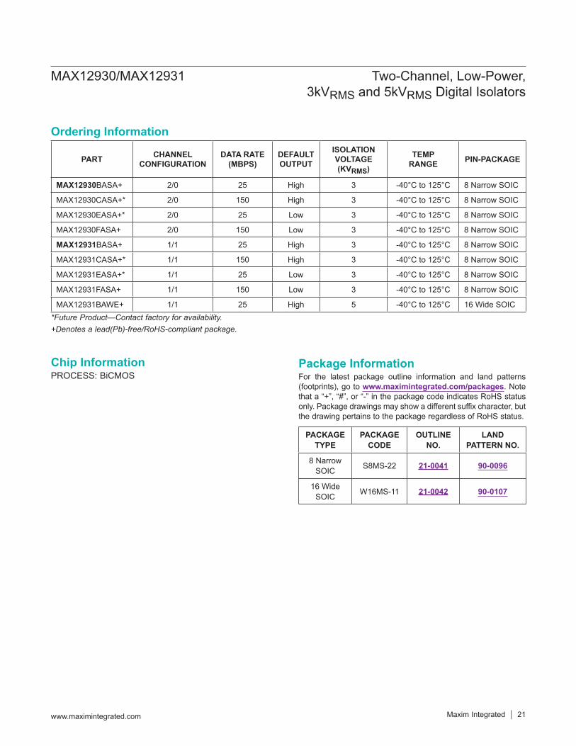
Ordering Information
Chip InformationPROCESS: BiCMOS
Package InformationFor the latest package outline information and land patterns (footprints), go to www.maximintegrated.com/packages. Note that a “+”, “#”, or “-” in the package code indicates RoHS status only. Package drawings may show a different suffix character, but the drawing pertains to the package regardless of RoHS status.
PART CHANNEL CONFIGURATION
DATA RATE (MBPS)
DEFAULT OUTPUT
ISOLATION VOLTAGE (KVRMS)
TEMP RANGE PIN-PACKAGE
MAX12930BASA+ 2/0 25 High 3 -40°C to 125°C 8 Narrow SOIC
MAX12930CASA+* 2/0 150 High 3 -40°C to 125°C 8 Narrow SOIC
MAX12930EASA+* 2/0 25 Low 3 -40°C to 125°C 8 Narrow SOIC
MAX12930FASA+ 2/0 150 Low 3 -40°C to 125°C 8 Narrow SOIC
MAX12931BASA+ 1/1 25 High 3 -40°C to 125°C 8 Narrow SOIC
MAX12931CASA+* 1/1 150 High 3 -40°C to 125°C 8 Narrow SOIC
MAX12931EASA+* 1/1 25 Low 3 -40°C to 125°C 8 Narrow SOIC
MAX12931FASA+ 1/1 150 Low 3 -40°C to 125°C 8 Narrow SOIC
MAX12931BAWE+ 1/1 25 High 5 -40°C to 125°C 16 Wide SOIC
PACKAGE TYPE
PACKAGE CODE
OUTLINE NO.
LAND PATTERN NO.
8 Narrow SOIC S8MS-22 21-0041 90-0096
16 Wide SOIC W16MS-11 21-0042 90-0107
*Future Product—Contact factory for availability.
Maxim Integrated cannot assume responsibility for use of any circuitry other than circuitry entirely embodied in a Maxim Integrated product. No circuit patent licenses are implied. Maxim Integrated reserves the right to change the circuitry and specifications without notice at any time. The parametric values (min and max limits) shown in the Electrical Characteristics table are guaranteed. Other parametric values quoted in this data sheet are provided for guidance.
Maxim Integrated and the Maxim Integrated logo are trademarks of Maxim Integrated Products, Inc.
MAX12930/MAX12931 Two-Channel, Low-Power, 3kVRMS and 5kVRMS Digital Isolators
© 2017 Maxim Integrated Products, Inc. 22
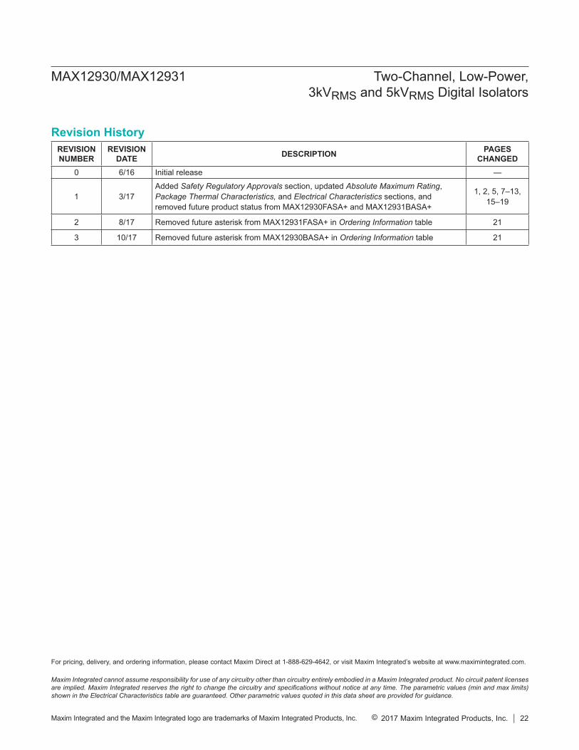
Revision HistoryREVISIONNUMBER
REVISIONDATE DESCRIPTION PAGES
CHANGED0 6/16 Initial release —
1 3/17Added Safety Regulatory Approvals section, updated Absolute Maximum Rating, Package Thermal Characteristics, and Electrical Characteristics sections, and removed future product status from MAX12930FASA+ and MAX12931BASA+
1, 2, 5, 7–13, 15–19
2 8/17 Removed future asterisk from MAX12931FASA+ in Ordering Information table 21
3 10/17 Removed future asterisk from MAX12930BASA+ in Ordering Information table 21
For pricing, delivery, and ordering information, please contact Maxim Direct at 1-888-629-4642, or visit Maxim Integrated’s website at www.maximintegrated.com.


![3.0V Core Async/Page PSRAM - ISSI · 3.0V Core Async/Page PSRAM ... Setting sleep enable (ZZ#) to LOW enables one of two low-power modes: ... [Top View] (Ball Down)](https://img.pdfslide.us/doc/110x75/5af6ee2e7f8b9a4d4d91165d/30v-core-asyncpage-psram-core-asyncpage-psram-setting-sleep-enable-zz.jpg)