Embed Size (px)
Citation preview
March 31, 2008
LME49600
High Performance, High Fidelity, High Current Audio BufferGeneral DescriptionThe LME49600 is a high performance, low distortion high fi-delity 250mA audio buffer. The LME49600 is designed for awide range of applications. It can be used inside the feedbackloop of op amps.
The LME49600 offers a pin-selectable bandwidth: a low cur-rent, 110MHz bandwidth mode that consumes 7.3mA and awide 180MHz bandwidth mode that consumes 13.2mA. Inboth modes the LME49600 has a nominal 2000V/μs slewrate. Bandwidth is easily adjusted by either leaving the BWpin unconnected or connecting a resistor between the BW pinand the VEE pin.
The LME49600 is fully protected through internal current limitand thermal shutdown.
Key Specifications
Low THD+N (VOUT = 3VRMS, f = 1kHz, Figure 2) 0.00003% (typ)
Slew Rate 2000V/μs (typ)
High Output Current 250mA (typ)
Bandwidth
BW pin floating 110MHz (typ)
BW connected to VEE 180MHz (typ)
Supply Voltage Range ±2.25V ≤ VS ≤ ±18V
Features Pin-selectable bandwidth and quiescent current
Pure fidelity. Pure performance
Short circuit protection
Thermal shutdown
TO–263 surface-mount package
Applications Headphone amplifier output drive stage
Line drivers
Low power audio amplifiers
High-current operational amplifier output stage
ATE Pin Driver Buffer
Power supply regulator
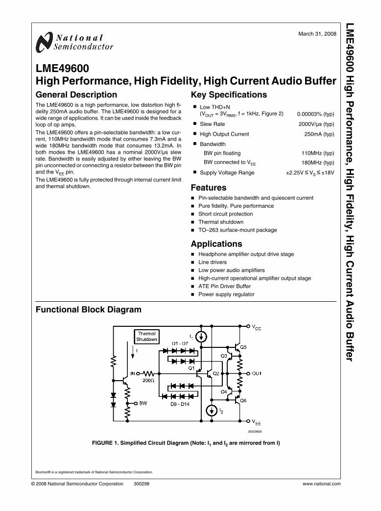
Functional Block Diagram
30029805
FIGURE 1. Simplified Circuit Diagram (Note: I1 and I2 are mirrored from I)
Boomer® is a registered trademark of National Semiconductor Corporation.
© 2008 National Semiconductor Corporation 300298 www.national.com
LM
E49600 H
igh
Perfo
rman
ce, H
igh
Fid
elity
, Hig
h C
urre
nt A
ud
io B
uffe
r
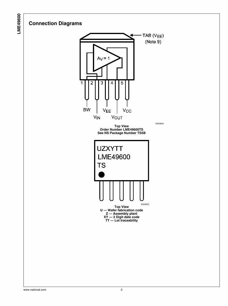
Connection Diagrams
300298a0
Top ViewOrder Number LME49600TS
See NS Package Number TS5B
30029832
Top ViewU — Wafer fabrication code
Z — Assembly plantXY — 2 Digit date codeTT — Lot traceability
www.national.com 2
LM
E49600

Absolute Maximum Ratings (Notes 1, 2)
If Military/Aerospace specified devices are required,please contact the National Semiconductor Sales Office/Distributors for availability and specifications.
Supply Voltage ±20V
ESD Ratings(Note 4) 2000V
ESD Ratings (Note 5) 200V
Storage Temperature −40°C to +150°C
Junction Temperature 150°C
Thermal Resistance
θJC4°C/W
θJA65°C/W
θJA (Note 3) 20°C/W
Soldering Information
TO-263 Package (10 seconds) 260°C
Operating Ratings (Notes 1, 2)
Temperature Range
TMIN ≤ TA ≤ TMAX −40°C ≤ TA ≤ 85°C
Supply Voltage ±2.25V to ±18V
System Electrical Characteristics for LME49600 The following specifications apply for VS = ±15V,
fIN = 1kHz, unless otherwise specified. Typicals and limits apply for TA = 25°C.
Symbol Parameter Conditions
LME49600Units
(Limits)Typical Limit
(Note 6) (Note 7)
IQ Total Quiescent Current
IOUT = 0
BW pin: No connect
BW pin: Connected to VEE pin
7.3
13.2
10.5
18
mA (max)
mA (max)
THD+NTotal Harmonic Distortion + Noise
(Note 8)
AV = 1, VOUT = 3VRMS, RL
= 32Ω, BW = 80kHz,
closed loop see Figure 2.
f = 1kHz
f = 20kHz
0.000035
0.0005
%
%
SR Slew Rate30 ≤ BW ≤ 180MHz
VOUT = 20VP-P, RL = 100Ω2000 V/μs
BW
Bandwidth
AV = –3dB
BW pin: No Connect
RL = 100ΩRL = 1kΩ
100
110
MHz
MHz
AV = –3dB
BW pin: Connected to VEE pin
RL = 100ΩRL = 1kΩ
160
180
MHz
MHz
Voltage Noise Density
f = 10kHz
BW pin: No Connect3.0 nV/√Hz
f = 10kHz
BW pin: Connected to VEE pin2.6 nV/√Hz
ts Settling Time
ΔV = 10V, RL = 100Ω1% Accuracy
BW pin: No connect
BW pin: Connected to VEE pin
200
60
ns
ns
AV Voltage Gain
VOUT = ±10V
RL = 67ΩRL = 100ΩRL = 1kΩ
0.93
0.95
0.99
0.90
0.92
0.98
V/V (min)
V/V (min)
V/V (min)
3 www.national.com
LM
E49600

Symbol Parameter Conditions
LME49600Units
(Limits)Typical Limit
(Note 6) (Note 7)
VOUT Voltage Output
Positive
IOUT = 10mA
IOUT = 100mA
IOUT = 150mA
VCC –1.4
VCC –2.0
VCC –2.3
VCC –1.6
VCC –2.1
VCC –2.7
V (min)
V (min)
V (min)
Negative
IOUT = –10mA
IOUT = –100mA
IOUT = –150mA
VEE +1.5
VEE +3.1
VEE +3.5
VEE +1.6
VEE +2.4
VEE +3.2
V (min)
V (min)
V (min)
IOUT Output Current ±250 mA
IOUT-SC Short Circuit Output CurrentBW pin: No Connect
BW pin: Connected to VEE pin
±490
±490 ±550
mA (max)
mA (max)
IB Input Bias Current
VIN = 0V
BW pin: No Connect
BW pin: Connected to VEE pin
±1.0
±3.0
±2.5
±5.0
μA (max)
μA (max)
ZIN Input Impedance
RL = 100ΩBW pin: No Connect
BW pin: Connected to VEE pin
7.5
5.5
MΩMΩ
VOS Offset Voltage ±17 ±60 mV (max)
VOS/°C Offset Voltage vs Temperature 40°C ≤ TA ≤ +125°C ±100 μV/°C
Note 1: All voltages are measured with respect to ground, unless otherwise specified.
Note 2: Absolute Maximum Ratings indicate limits beyond which damage to the device may occur. Operating Ratings indicate conditions for which the device isfunctional, but do not guarantee specific performance limits. Electrical Characteristics state DC and AC electrical specifications under particular test conditionswhich guarantee specific performance limits. This assumes that the device is within the Operating Ratings. Specifications are not guaranteed for parameterswhere no limit is given, however, the typical value is a good indication of device performance.
Note 3: The maximum power dissipation must be derated at elevated temperatures and is dictated by TJMAX, θJA, and the ambient temperature TA. The maximumallowable power dissipation is PDMAX = (TJMAX–TA)/θJA or the number given in Absolute Maximum Ratings, whichever is lower. For the LME49600, typicalapplication (shown in Figure 2) with VSUPPLY = 30V, RL = 32Ω, the total power dissipation is 1.9W. θJA = 20°C/W for the TO–263 package mounted to 16in2 1ozcopper surface heat sink area.
Note 4: Human body model, 100pF discharged through a 1.5kΩ resistor.
Note 5: Machine Model, 220pF – 240pF discharged through all pins.
Note 6: Typical specifications are specified at 25°C and represent the parametric norm.
Note 7: Tested limits are guaranteed to National's AOQL (Average Outgoing Quality Level).
Note 8: This is the distortion of the LME49600 operating in a closed loop configuration with an LME49710. When operating in an operational amplifier's feedbackloop, the amplifier’s open loop gain dominates, linearizing the system and determining the overall system distortion.
Note 9: The TSB package is non-isolated package. The package's metal back and any heat sink to which it is mounted are connected to the same potential asthe -VEE pin.
www.national.com 4
LM
E49600
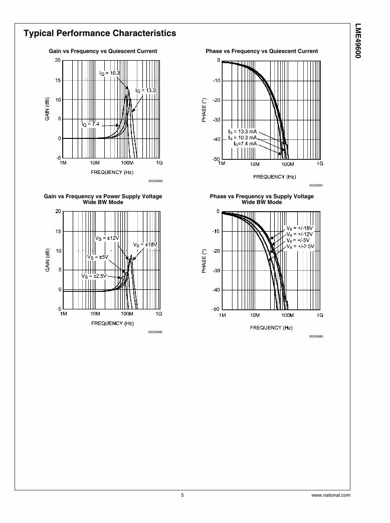
Typical Performance Characteristics
Gain vs Frequency vs Quiescent Current
30029899
Phase vs Frequency vs Quiescent Current
30029881
Gain vs Frequency vs Power Supply VoltageWide BW Mode
30029898
Phase vs Frequency vs Supply VoltageWide BW Mode
30029880
5 www.national.com
LM
E49600
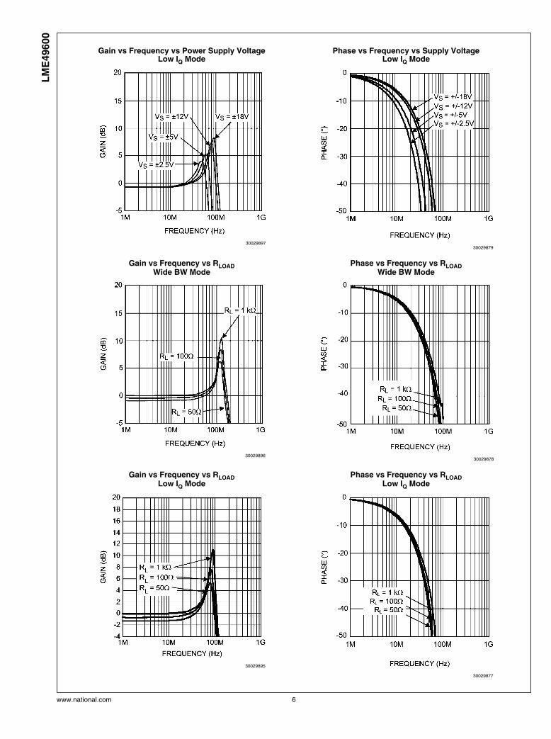
Gain vs Frequency vs Power Supply VoltageLow IQ Mode
30029897
Phase vs Frequency vs Supply VoltageLow IQ Mode
30029879
Gain vs Frequency vs RLOADWide BW Mode
30029896
Phase vs Frequency vs RLOADWide BW Mode
30029878
Gain vs Frequency vs RLOADLow IQ Mode
30029895
Phase vs Frequency vs RLOADLow IQ Mode
30029877
www.national.com 6
LM
E49600
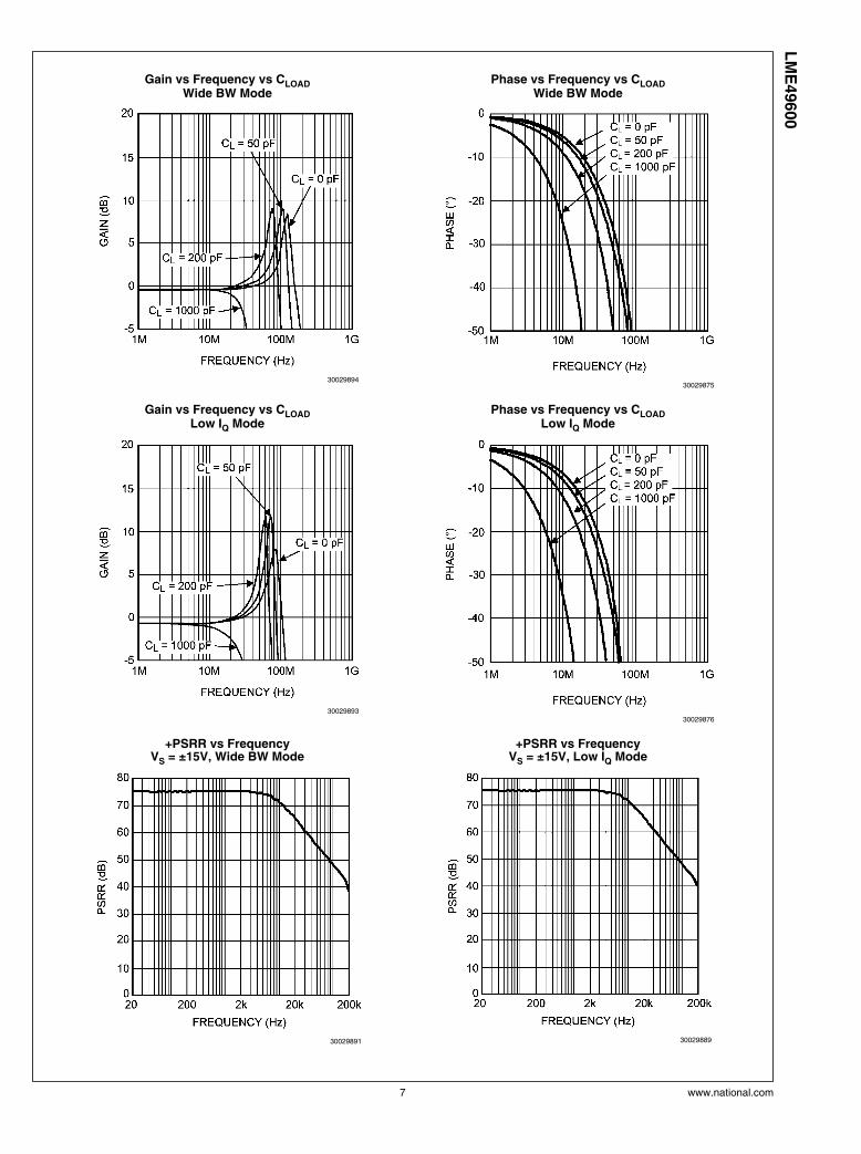
Gain vs Frequency vs CLOADWide BW Mode
30029894
Phase vs Frequency vs CLOADWide BW Mode
30029875
Gain vs Frequency vs CLOADLow IQ Mode
30029893
Phase vs Frequency vs CLOADLow IQ Mode
30029876
+PSRR vs FrequencyVS = ±15V, Wide BW Mode
30029891
+PSRR vs FrequencyVS = ±15V, Low IQ Mode
30029889
7 www.national.com
LM
E49600

+PSRR vs FrequencyVS = ±15V, Wide BW Mode
30029892
+PSRR vs FrequencyVS = ±15V, Low IQ Mode
30029890
Quiescent Current vs Bandwidth Control Resistance
30029888
THD+N vs Output VoltageVS = ±15V, RL = 32Ω, f = 1kHz
Both channels driven
300298j4
High BW Noise Curve
30029845
Low BW Noise Curve
30029846
www.national.com 8
LM
E49600
Typical Application Diagram
300298j5
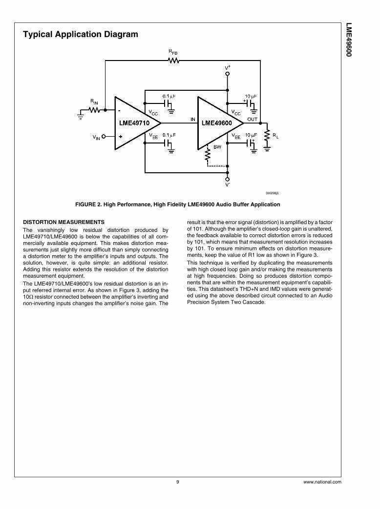
FIGURE 2. High Performance, High Fidelity LME49600 Audio Buffer Application
DISTORTION MEASUREMENTS
The vanishingly low residual distortion produced byLME49710/LME49600 is below the capabilities of all com-mercially available equipment. This makes distortion mea-surements just slightly more difficult than simply connectinga distortion meter to the amplifier’s inputs and outputs. Thesolution, however, is quite simple: an additional resistor.Adding this resistor extends the resolution of the distortionmeasurement equipment.
The LME49710/LME49600’s low residual distortion is an in-put referred internal error. As shown in Figure 3, adding the10Ω resistor connected between the amplifier’s inverting andnon-inverting inputs changes the amplifier’s noise gain. The
result is that the error signal (distortion) is amplified by a factorof 101. Although the amplifier’s closed-loop gain is unaltered,the feedback available to correct distortion errors is reducedby 101, which means that measurement resolution increasesby 101. To ensure minimum effects on distortion measure-ments, keep the value of R1 low as shown in Figure 3.
This technique is verified by duplicating the measurementswith high closed loop gain and/or making the measurementsat high frequencies. Doing so produces distortion compo-nents that are within the measurement equipment’s capabili-ties. This datasheet’s THD+N and IMD values were generat-ed using the above described circuit connected to an AudioPrecision System Two Cascade.
9 www.national.com
LM
E49600
30029843
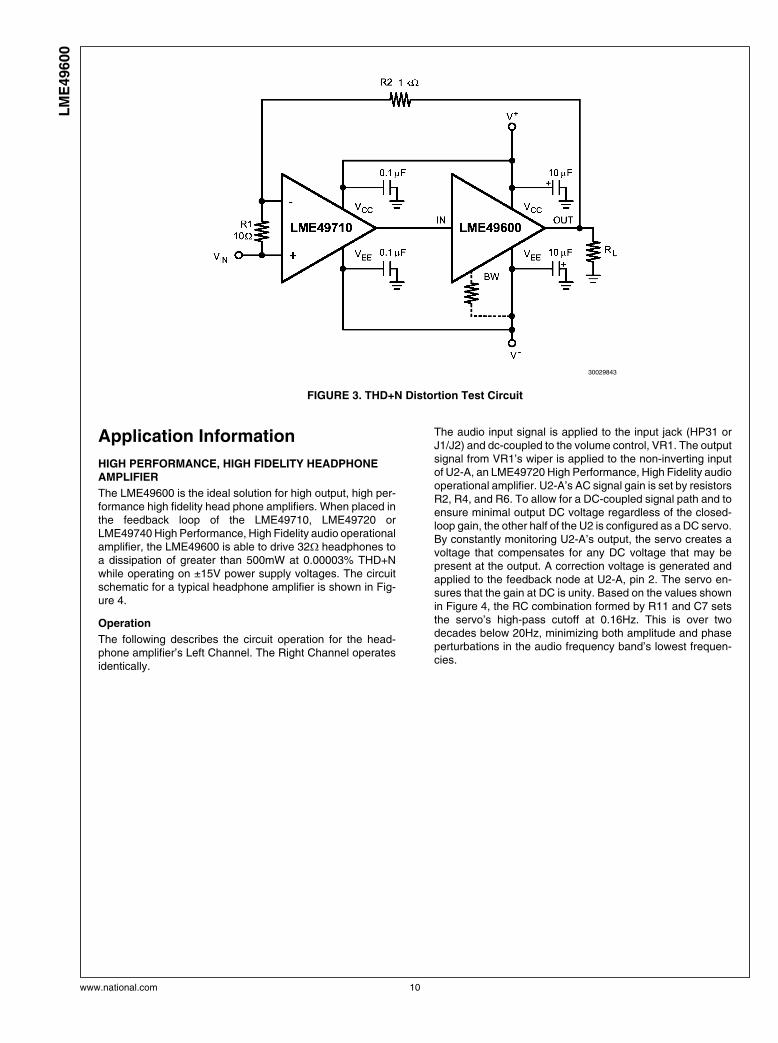
FIGURE 3. THD+N Distortion Test Circuit
Application Information
HIGH PERFORMANCE, HIGH FIDELITY HEADPHONEAMPLIFIER
The LME49600 is the ideal solution for high output, high per-formance high fidelity head phone amplifiers. When placed inthe feedback loop of the LME49710, LME49720 orLME49740 High Performance, High Fidelity audio operationalamplifier, the LME49600 is able to drive 32Ω headphones toa dissipation of greater than 500mW at 0.00003% THD+Nwhile operating on ±15V power supply voltages. The circuitschematic for a typical headphone amplifier is shown in Fig-ure 4.
Operation
The following describes the circuit operation for the head-phone amplifier’s Left Channel. The Right Channel operatesidentically.
The audio input signal is applied to the input jack (HP31 orJ1/J2) and dc-coupled to the volume control, VR1. The outputsignal from VR1’s wiper is applied to the non-inverting inputof U2-A, an LME49720 High Performance, High Fidelity audiooperational amplifier. U2-A’s AC signal gain is set by resistorsR2, R4, and R6. To allow for a DC-coupled signal path and toensure minimal output DC voltage regardless of the closed-loop gain, the other half of the U2 is configured as a DC servo.By constantly monitoring U2-A’s output, the servo creates avoltage that compensates for any DC voltage that may bepresent at the output. A correction voltage is generated andapplied to the feedback node at U2-A, pin 2. The servo en-sures that the gain at DC is unity. Based on the values shownin Figure 4, the RC combination formed by R11 and C7 setsthe servo’s high-pass cutoff at 0.16Hz. This is over twodecades below 20Hz, minimizing both amplitude and phaseperturbations in the audio frequency band’s lowest frequen-cies.
www.national.com 10
LM
E49600
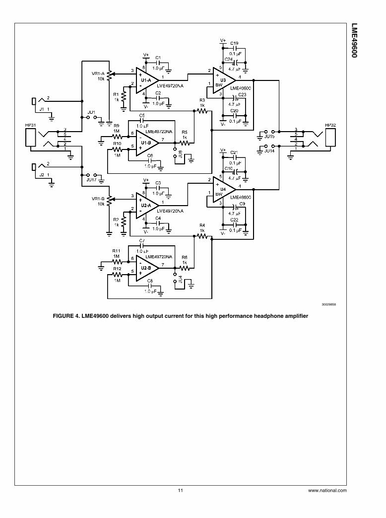
30029858
FIGURE 4. LME49600 delivers high output current for this high performance headphone amplifier
11 www.national.com
LM
E49600

AUDIO BUFFERS
Audio buffers or unity-gain followers, have large current gainand a voltage gain of one. Audio buffers serve many applica-tions that require high input impedance, low outputimpedance and high output current. They also offer constantgain over a very wide bandwidth.
Buffers serve several useful functions, either in stand-aloneapplications or in tandem with operational amplifiers. In stand-alone applications, their high input impedance and low outputimpedance isolates a high impedance source from a lowimpedance load.
SUPPLY BYPASSING
The LME49600 will place great demands on the power supplyvoltage source when operating in applications that requirefast slewing and driving heavy loads. These conditions cancreate high amplitude transient currents. A power supply’slimited bandwidth can reduce the supply’s ability to supply theneeded current demands during these high slew rate condi-tions. This inability to supply the current demand is furtherexacerbated by PCB trace or interconnecting wire induc-tance. The transient current flowing through the inductancecan produce voltage transients.
For example, the LME49600’s output voltage can slew at atypical ±2000V/μs. When driving a 100Ω load, the di/dt currentdemand is 20 A/μs. This current flowing through an induc-tance of 50nH (approximately 1.5” of 22 gage wire) will pro-duce a 1V transient. In these and similar situations, place theparallel combination of a solid 5μF to 10μF tantalum capacitorand a ceramic 0.1μF capacitor as close as possible to thedevice supply pins.
Ceramic capacitors with values in the range of 10μF to100μF, ceramic capacitor have very lower ESR (typically lessthan 10mΩ) and low ESL when compared to the same valuedtantalum capacitor. The ceramic capacitors, therefore, havesuperior AC performance for bypassing high frequency noise.
In less demanding applications that have lighter loads or low-er slew rates, the supply bypassing is not as critical. Capacitorvalues in the range of 0.01μF to 0.1μF are adequate.
SIMPLIFIED LME49600 CIRCUIT DIAGRAM
The LME49600’s simplified circuit diagram is shown in Fig-ures 1 and 5. The diagram shows the LME49600’s comple-mentary emitter follower design, bias circuit and bandwidthadjustment node.
30029805
FIGURE 5. Simplified Circuit Diagram
Figure 6 shows the LME49600 connected as an open-loopbuffer. The source impedance and optional input resistor,RS, can alter the frequency response. As previously stated,the power supplies should be bypassed with capacitors con-nected close to the LME49600’s power supply pins. Capacitorvalues as low as 0.01μF to 0.1μF will ensure stable operationin lightly loaded applications, but high output current and fastoutput slewing can demand large current transients from thepower supplies. Place a recommended parallel combinationof a solid tantalum capacitor in the 5μF to 10μF range and aceramic 0.1μF capacitor as close as possible to the devicesupply pins.
30029860
FIGURE 6. Buffer Connections
OUTPUT CURRENT
The LME49600 can continuously source or sink 250mA. In-ternal circuitry limits the short circuit output current to approx-imately ±450mA. For many applications that fully utilize theLME49600’s current source and sink capabilities, thermal dis-sipation may be the factor that limits the continuous outputcurrent.
The maximum output voltage swing magnitude varies withjunction temperature and output current. Using sufficient PCBcopper area as a heat sink when the metal tab of theLME49600’s surface mount TO–263 package is soldered di-rectly to the circuit board reduces thermal impedance. This inturn reduces junction temperature. The PCB copper areashould be in the range of 3in2 (12.9cm2) to 6in2 (38.7cm2).
THERMAL PROTECTION
LME49600 power dissipated will cause the buffer’s junctiontemperature to rise. A thermal protection circuit in theLME49600 will disable the output when the junction temper-ature exceeds 150°C. When the thermal protection is activat-ed, the output stage is disabled, allowing the device to cool.The output circuitry is enabled when the junction temperaturedrops below 150°C.
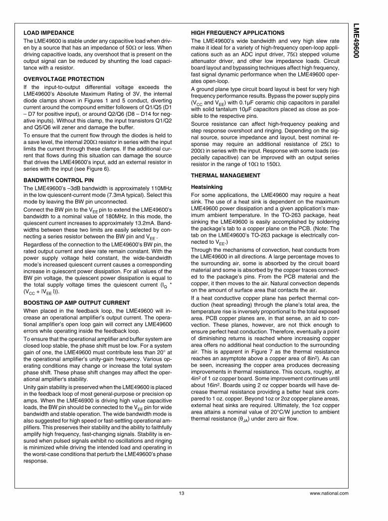
The TO–263 package has excellent thermal characteristics.To minimize thermal impedance, its exposed die attach pad-dle should be soldered to a circuit board copper area for goodheat dissipation. Figure 7 shows typical thermal resistancefrom junction to ambient as a function of the copper area. TheTO–263’s exposed die attach paddle is electrically connectedto the VEE power supply pin.
www.national.com 12
LM
E49600
LOAD IMPEDANCE
The LME49600 is stable under any capacitive load when driv-en by a source that has an impedance of 50Ω or less. Whendriving capacitive loads, any overshoot that is present on theoutput signal can be reduced by shunting the load capaci-tance with a resistor.
OVERVOLTAGE PROTECTION
If the input-to-output differential voltage exceeds theLME49600’s Absolute Maximum Rating of 3V, the internaldiode clamps shown in Figures 1 and 5 conduct, divertingcurrent around the compound emitter followers of Q1/Q5 (D1– D7 for positive input), or around Q2/Q6 (D8 – D14 for neg-ative inputs). Without this clamp, the input transistors Q1/Q2and Q5/Q6 will zener and damage the buffer.
To ensure that the current flow through the diodes is held toa save level, the internal 200Ω resistor in series with the inputlimits the current through these clamps. If the additional cur-rent that flows during this situation can damage the sourcethat drives the LME49600’s input, add an external resistor inseries with the input (see Figure 6).
BANDWITH CONTROL PIN
The LME49600’s –3dB bandwidth is approximately 110MHzin the low quiescent-current mode (7.3mA typical). Select thismode by leaving the BW pin unconnected.
Connect the BW pin to the VEE pin to extend the LME49600’sbandwidth to a nominal value of 180MHz. In this mode, thequiescent current increases to approximately 13.2mA. Band-widths between these two limits are easily selected by con-necting a series resistor between the BW pin and VEE .
Regardless of the connection to the LME49600’s BW pin, therated output current and slew rate remain constant. With thepower supply voltage held constant, the wide-bandwidthmode’s increased quiescent current causes a correspondingincrease in quiescent power dissipation. For all values of theBW pin voltage, the quiescent power dissipation is equal tothe total supply voltage times the quiescent current (IQ *(VCC + |VEE |)).
BOOSTING OP AMP OUTPUT CURRENT
When placed in the feedback loop, the LME49600 will in-crease an operational amplifier’s output current. The opera-tional amplifier’s open loop gain will correct any LME49600errors while operating inside the feedback loop.
To ensure that the operational amplifier and buffer system areclosed loop stable, the phase shift must be low. For a systemgain of one, the LME49600 must contribute less than 20° atthe operational amplifier’s unity-gain frequency. Various op-erating conditions may change or increase the total systemphase shift. These phase shift changes may affect the oper-ational amplifier's stability.
Unity gain stability is preserved when the LME49600 is placedin the feedback loop of most general-purpose or precision opamps. When the LME46900 is driving high value capacitiveloads, the BW pin should be connected to the VEE pin for widebandwidth and stable operation. The wide bandwidth mode isalso suggested for high speed or fast-settling operational am-plifiers. This preserves their stability and the ability to faithfullyamplify high frequency, fast-changing signals. Stability is en-sured when pulsed signals exhibit no oscillations and ringingis minimized while driving the intended load and operating inthe worst-case conditions that perturb the LME49600’s phaseresponse.
HIGH FREQUENCY APPLICATIONS
The LME49600’s wide bandwidth and very high slew ratemake it ideal for a variety of high-frequency open-loop appli-cations such as an ADC input driver, 75Ω stepped volumeattenuator driver, and other low impedance loads. Circuitboard layout and bypassing techniques affect high frequency,fast signal dynamic performance when the LME49600 oper-ates open-loop.
A ground plane type circuit board layout is best for very highfrequency performance results. Bypass the power supply pins(VCC and VEE) with 0.1μF ceramic chip capacitors in parallelwith solid tantalum 10μF capacitors placed as close as pos-sible to the respective pins.
Source resistance can affect high-frequency peaking andstep response overshoot and ringing. Depending on the sig-nal source, source impedance and layout, best nominal re-sponse may require an additional resistance of 25Ω to200Ω in series with the input. Response with some loads (es-pecially capacitive) can be improved with an output seriesresistor in the range of 10Ω to 150Ω.
THERMAL MANAGEMENT
Heatsinking
For some applications, the LME49600 may require a heatsink. The use of a heat sink is dependent on the maximumLME49600 power dissipation and a given application’s max-imum ambient temperature. In the TO-263 package, heatsinking the LME49600 is easily accomplished by solderingthe package’s tab to a copper plane on the PCB. (Note: Thetab on the LME49600’s TO-263 package is electrically con-nected to VEE.)
Through the mechanisms of convection, heat conducts fromthe LME49600 in all directions. A large percentage moves tothe surrounding air, some is absorbed by the circuit boardmaterial and some is absorbed by the copper traces connect-ed to the package’s pins. From the PCB material and thecopper, it then moves to the air. Natural convection dependson the amount of surface area that contacts the air.
If a heat conductive copper plane has perfect thermal con-duction (heat spreading) through the plane’s total area, thetemperature rise is inversely proportional to the total exposedarea. PCB copper planes are, in that sense, an aid to con-vection. These planes, however, are not thick enough toensure perfect heat conduction. Therefore, eventually a pointof diminishing returns is reached where increasing copperarea offers no additional heat conduction to the surroundingair. This is apparent in Figure 7 as the thermal resistancereaches an asymptote above a copper area of 8in2). As canbe seen, increasing the copper area produces decreasingimprovements in thermal resistance. This occurs, roughly, at4in2 of 1 oz copper board. Some improvement continues untilabout 16in2. Boards using 2 oz copper boards will have de-crease thermal resistance providing a better heat sink com-pared to 1 oz. copper. Beyond 1oz or 2oz copper plane areas,external heat sinks are required. Ultimately, the 1oz copperarea attains a nominal value of 20°C/W junction to ambientthermal resistance (θJA) under zero air flow.
13 www.national.com
LM
E49600
30029861
FIGURE 7. Thermal Resistance for 5 lead TO–263Package Mounted on 1oz. Copper
A copper plane may be placed directly beneath the tab. Ad-ditionally, a matching plane can be placed on the oppositeside. If a plane is placed on the side opposite of theLME49600, connect it to the plane to which the buffer’s metaltab is soldered with a matrix of thermal vias per JEDEC Stan-dard JESD51-5.
Determining Copper Area
Find the required copper heat sink area using the followingguidelines:
1. Determine the value of the circuit’s power dissipation, PD.
2. Specify a maximum operating ambient temperature, TA
(MAX). (Note that the die temperature, TJ, will be higher thanTA by an amount that is dependent on the thermal resistancefrom junction to ambient, θJA). Therefore, TA must be speci-fied such that TJ does not exceed the absolute maximum dietemperature of 150°C.
3. Specify a maximum allowable junction temperature, TJ
(MAX), This is the LME49600’s die temperature when the bufferis drawing maximum current (quiescent and load). It is pru-dent to design for a maximum continuous junction tempera-ture of 100°C to 130°C. Ensure, however, that the junctiontemperature never exceeds the 150°C absolute maximumrating for the part.
4. Calculate the value of junction to ambient thermal resis-tance, θJA
5. θJA as a function of copper area in square inches is shownin Figure 7. Choose a copper area that will guarantee thespecified TJ(MAX) for the calculated θJA. The maximum valueof junction to ambient thermal resistance, θJA, is defined as:
θJA= (TJ(MAX) - TA(MAX) )/ PD(MAX) (°C/W) (1)
where:
TJ(MAX) = the maximum recommended junction temperature
TA(MAX) = the maximum ambient temperature in theLME49600’s environment
PD(MAX) = the maximum recommended power dissipation
Note: The allowable thermal resistance is determined by themaximum allowable temperature increase:
TRISE = TJ(MAX) - TA(MAX)
Thus, if ambient temperature extremes force TRISE to exceedthe design maximum, the part must be de-rated by either de-creasing PD to a safe level, reducing θJA further or, if available,using a larger copper area.
Procedure
1. First determine the maximum power dissipated by theLME49600, PD(MAX). For the simple case of the buffer drivinga resistive load, and assuming equal supplies, PD(MAX) is giv-en by:
PDMAX(AC) = (IS x VS) + (VS)2 / (2π2RL) (Watts) (2)
PDMAX(DC) = (IS x VS) + (VS)2 / RL (Watts) (3)
where:
VS = |VEE| + VCC (V)
IS =quiescent supply current (A)
Equation (2) is for sinusoidal output voltages and (3) is for DCoutput voltages
2. Determine the maximum allowable die temperature rise,
TRISE(MAX) = TJ(MAX) - TA(MAX) (°C)
3. Using the calculated value of TRISE(MAX) and PD(MAX), findthe required value of junction to ambient thermal resistancecombining equation 1 and equation 4 to derive equation 5:
θJA = TRISE(MAX) / PD(MAX) (4)
4. Finally, choose the minimum value of copper area fromFigure 7 based on the value for θJA.
Example
Assume the following conditions: VS = |VEE| + VCC = 30V, RL= 32Ω, IS = 15mA, sinusoidal output voltage, TJ(MAX) = 125°C, TA(MAX) = 85°C.
Applying Equation (2):
PDMAX = (IS x VS) + (VS)2 / 2π2RL
= (15mA)(30V) + 900V2 / 142Ω= 1.86W
Applying Equation (4):
TRISE(MAX) = 125°C – 85°C
= 40°C
Applying Equation (5):
θJA = 40°C/1.86W
= 21.5°C/W
www.national.com 14
LM
E49600
Examining the Copper Area vs. θJA plot indicates that a ther-mal resistance of 50°C/W is possible with a 12in2 plane of onelayer of 1oz copper. Other solutions include using two layersof 1oz copper or the use of 2oz copper. Higher dissipationmay require forced air flow. As a safety margin, an extra 15%heat sinking capability is recommended.
When amplifying AC signals, wave shapes and the nature ofthe load (reactive, non-reactive) also influence dissipation.Peak dissipation can be several times the average with reac-tive loads. It is particularly important to determine dissipationwhen driving large load capacitance.
The LME49600’s dissipation in DC circuit applications is eas-ily computed using Equation (3). After the value of dissipationis determined, the heat sink copper area calculation is thesame as for AC signals.
SLEW RATE
A buffer’s voltage slew rate is its output signal’s rate of changewith respect to an input signal’s step changes. For resistive
loads, slew rate is limited by internal circuit capacitance andoperating current (in general, the higher the operating currentfor a given internal capacitance, the faster the slew rate).
However, when driving capacitive loads, the slew rate may belimited by the available peak output current according to thefollowing expression.
dv/dt = IPK / CL (5)
Output voltages with high slew rates will require large outputload currents. For example if the part is required to slew at1000V/μs with a load capacitance of 1nF, the current de-manded from the LME49600 is 1A. Therefore, fast slew rateis incompatible with a capacitive load of this value. Also, ifCL is in parallel with the load, the peak current available to theload decreases as CL increases.
15 www.national.com
LM
E49600
30029844
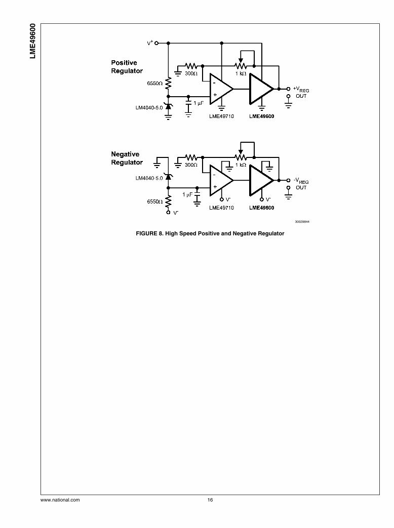
FIGURE 8. High Speed Positive and Negative Regulator
www.national.com 16
LM
E49600
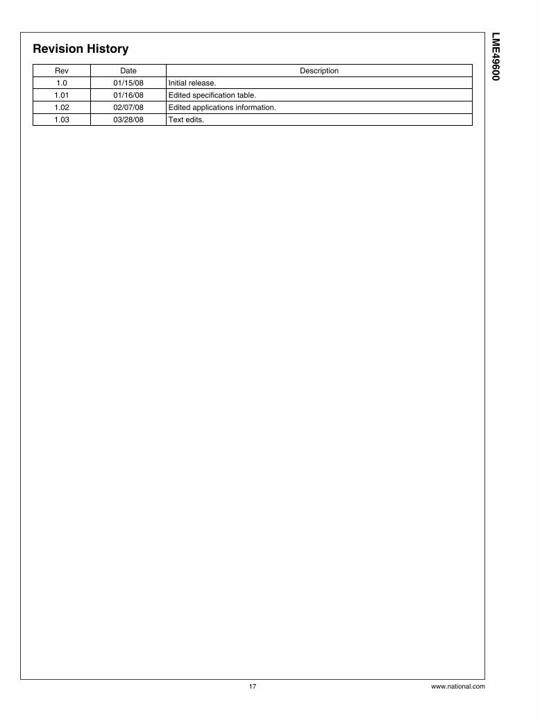
Revision History
Rev Date Description
1.0 01/15/08 Initial release.
1.01 01/16/08 Edited specification table.
1.02 02/07/08 Edited applications information.
1.03 03/28/08 Text edits.
17 www.national.com
LM
E49600
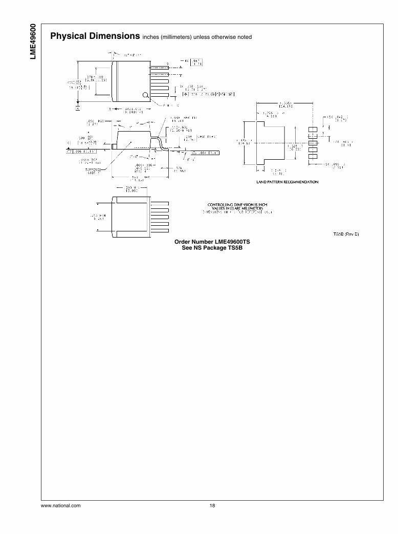
Physical Dimensions inches (millimeters) unless otherwise noted
Order Number LME49600TSSee NS Package TS5B
www.national.com 18
LM
E49600

Notes
19 www.national.com
LM
E49600

NotesL
ME
49600 H
igh
Perf
orm
an
ce, H
igh
Fid
elity
, H
igh
Cu
rren
t A
ud
io B
uff
er
For more National Semiconductor product information and proven design tools, visit the following Web sites at:
Products Design Support
Amplifiers www.national.com/amplifiers WEBENCH www.national.com/webench
Audio www.national.com/audio Analog University www.national.com/AU
Clock Conditioners www.national.com/timing App Notes www.national.com/appnotes
Data Converters www.national.com/adc Distributors www.national.com/contacts
Displays www.national.com/displays Green Compliance www.national.com/quality/green
Ethernet www.national.com/ethernet Packaging www.national.com/packaging
Interface www.national.com/interface Quality and Reliability www.national.com/quality
LVDS www.national.com/lvds Reference Designs www.national.com/refdesigns
Power Management www.national.com/power Feedback www.national.com/feedback
Switching Regulators www.national.com/switchers
LDOs www.national.com/ldo
LED Lighting www.national.com/led
PowerWise www.national.com/powerwise
Serial Digital Interface (SDI) www.national.com/sdi
Temperature Sensors www.national.com/tempsensors
Wireless (PLL/VCO) www.national.com/wireless
THE CONTENTS OF THIS DOCUMENT ARE PROVIDED IN CONNECTION WITH NATIONAL SEMICONDUCTOR CORPORATION(“NATIONAL”) PRODUCTS. NATIONAL MAKES NO REPRESENTATIONS OR WARRANTIES WITH RESPECT TO THE ACCURACYOR COMPLETENESS OF THE CONTENTS OF THIS PUBLICATION AND RESERVES THE RIGHT TO MAKE CHANGES TOSPECIFICATIONS AND PRODUCT DESCRIPTIONS AT ANY TIME WITHOUT NOTICE. NO LICENSE, WHETHER EXPRESS,IMPLIED, ARISING BY ESTOPPEL OR OTHERWISE, TO ANY INTELLECTUAL PROPERTY RIGHTS IS GRANTED BY THISDOCUMENT.
TESTING AND OTHER QUALITY CONTROLS ARE USED TO THE EXTENT NATIONAL DEEMS NECESSARY TO SUPPORTNATIONAL’S PRODUCT WARRANTY. EXCEPT WHERE MANDATED BY GOVERNMENT REQUIREMENTS, TESTING OF ALLPARAMETERS OF EACH PRODUCT IS NOT NECESSARILY PERFORMED. NATIONAL ASSUMES NO LIABILITY FORAPPLICATIONS ASSISTANCE OR BUYER PRODUCT DESIGN. BUYERS ARE RESPONSIBLE FOR THEIR PRODUCTS ANDAPPLICATIONS USING NATIONAL COMPONENTS. PRIOR TO USING OR DISTRIBUTING ANY PRODUCTS THAT INCLUDENATIONAL COMPONENTS, BUYERS SHOULD PROVIDE ADEQUATE DESIGN, TESTING AND OPERATING SAFEGUARDS.
EXCEPT AS PROVIDED IN NATIONAL’S TERMS AND CONDITIONS OF SALE FOR SUCH PRODUCTS, NATIONAL ASSUMES NOLIABILITY WHATSOEVER, AND NATIONAL DISCLAIMS ANY EXPRESS OR IMPLIED WARRANTY RELATING TO THE SALEAND/OR USE OF NATIONAL PRODUCTS INCLUDING LIABILITY OR WARRANTIES RELATING TO FITNESS FOR A PARTICULARPURPOSE, MERCHANTABILITY, OR INFRINGEMENT OF ANY PATENT, COPYRIGHT OR OTHER INTELLECTUAL PROPERTYRIGHT.
LIFE SUPPORT POLICY
NATIONAL’S PRODUCTS ARE NOT AUTHORIZED FOR USE AS CRITICAL COMPONENTS IN LIFE SUPPORT DEVICES ORSYSTEMS WITHOUT THE EXPRESS PRIOR WRITTEN APPROVAL OF THE CHIEF EXECUTIVE OFFICER AND GENERALCOUNSEL OF NATIONAL SEMICONDUCTOR CORPORATION. As used herein:
Life support devices or systems are devices which (a) are intended for surgical implant into the body, or (b) support or sustain life andwhose failure to perform when properly used in accordance with instructions for use provided in the labeling can be reasonably expectedto result in a significant injury to the user. A critical component is any component in a life support device or system whose failure to performcan be reasonably expected to cause the failure of the life support device or system or to affect its safety or effectiveness.
National Semiconductor and the National Semiconductor logo are registered trademarks of National Semiconductor Corporation. All otherbrand or product names may be trademarks or registered trademarks of their respective holders.
Copyright© 2008 National Semiconductor Corporation
For the most current product information visit us at www.national.com
National SemiconductorAmericas TechnicalSupport CenterEmail:[email protected]: 1-800-272-9959
National Semiconductor EuropeTechnical Support CenterEmail: [email protected] Tel: +49 (0) 180 5010 771English Tel: +44 (0) 870 850 4288
National Semiconductor AsiaPacific Technical Support CenterEmail: [email protected]
National Semiconductor JapanTechnical Support CenterEmail: [email protected]
www.national.com