Embed Size (px)
Citation preview
OUTIN
GND
LP38513-ADJ
VIN VOUT
ENVEN
CIN10 PF
Ceramic COUT10 PFCeramic
GND GND
ONOFF
CFFADJ
R1
R2
LP38513-ADJ
www.ti.com SNVS514C –JANUARY 2009–REVISED APRIL 2013
LP38513-ADJ 3A Fast-Transient Response Adjustable Low-Dropout Linear VoltageRegulator
Check for Samples: LP38513-ADJ
1FEATURES APPLICATIONS2• 2.25V to 5.5V Input Voltage Range • Digital Core ASICs, FPGAs, and DSPs• Adjustable Output Voltage Range of 0.5V to • Servers
4.5V • Routers and Switches• 3.0A Output Load Current • Base Stations• ±2.0% Accuracy over Line, Load, and Full- • Storage Area Networks
Temperature Range from -40°C to +125°C • DDR2 Memory• Stable with tiny 10 µF ceramic capacitors• Enable pin DESCRIPTION
The LP38513-ADJ Fast-Transient Response Low-• Typically less than 1 µA of Ground pin currentDropout Voltage Regulator offers the highest-when Enable pin is lowperformance in meeting AC and DC accuracy• 25dB of PSRR at 100 kHz requirements for powering Digital Cores. The
• Over-Temperature and Over-Current LP38513-ADJ uses a proprietary control loop thatProtection enables extremely fast response to change in line
conditions and load demands. Output Voltage DC• TO-263 THIN 5-Pin Surface Mount Packageaccuracy at 2.5% over line, load and full temperaturerange from -40°C to +125°C. The LP38513-ADJ isdesigned for inputs from the 2.5V, 3.3V, and 5.0V rail,is stable with 10 μF ceramic capacitors, and has anadjustable output voltage. The LP38513-ADJprovides excellent transient performance to meet thedemand of high performance digital core ASICs,DSPs, and FPGAs found in highly-intensiveapplications such as servers, routers/switches, andbase stations.
Typical Application Circuit
1
Please be aware that an important notice concerning availability, standard warranty, and use in critical applications ofTexas Instruments semiconductor products and disclaimers thereto appears at the end of this data sheet.
2All trademarks are the property of their respective owners.
PRODUCTION DATA information is current as of publication date. Copyright © 2009–2013, Texas Instruments IncorporatedProducts conform to specifications per the terms of the TexasInstruments standard warranty. Production processing does notnecessarily include testing of all parameters.
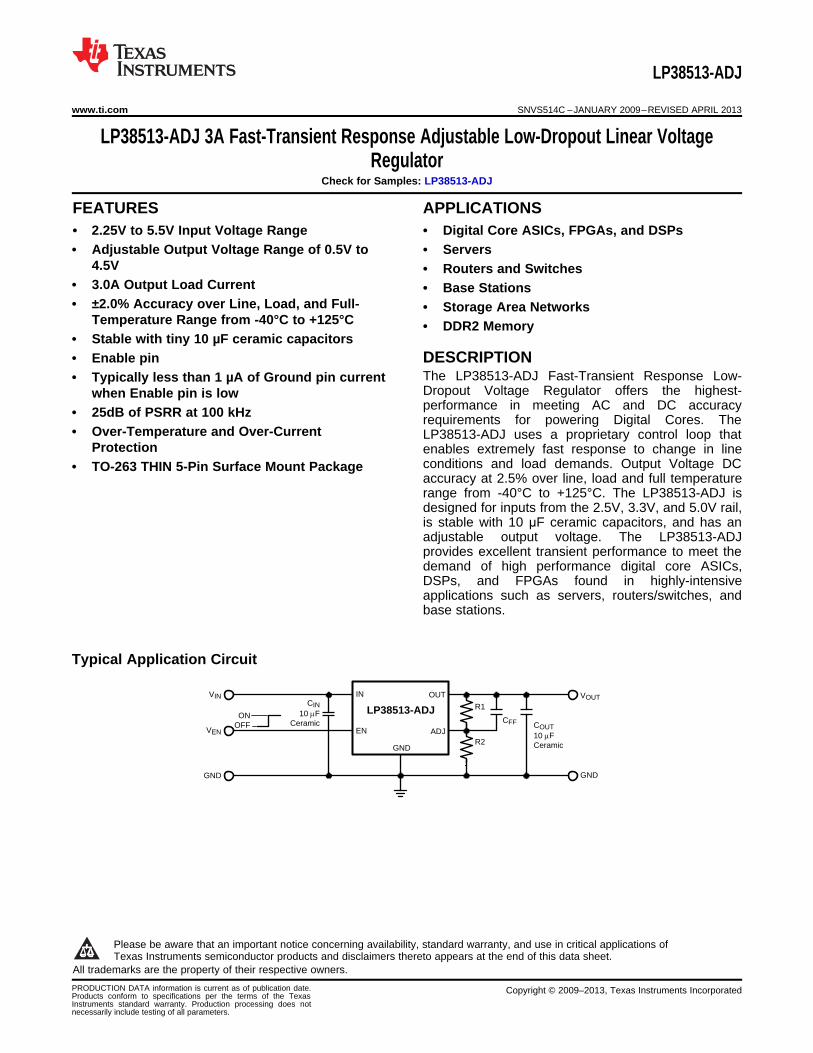
ExposedDAP
OUT
GND
EN 1
2
3
4
5
IN
LP
38513TJ-A
DJ
ADJ
LP38513-ADJ
SNVS514C –JANUARY 2009–REVISED APRIL 2013 www.ti.com
This integrated circuit can be damaged by ESD. Texas Instruments recommends that all integrated circuits be handled withappropriate precautions. Failure to observe proper handling and installation procedures can cause damage.
ESD damage can range from subtle performance degradation to complete device failure. Precision integrated circuits may be moresusceptible to damage because very small parametric changes could cause the device not to meet its published specifications.
Connection DiagramTop View
See Package Number NDQ0005A
Pin Descriptions for TO-263 THIN PackagePin # Pin Name Function
Enable. Pull high to enable the output, low to disable the output. This pin has no internal bias and1 EN must be tied to the input voltage, or actively driven.
2 IN Input Supply Pin
3 GND Ground
4 OUT Regulated Output Voltage Pin
5 ADJ The feedback to the internal Error Amplifier to set the output voltage
The TO-263 THIN DAP connection is used as a thermal connection to remove heat from the deviceto an external heat-sink in the form of the copper area on the printed circuit board. The DAP isDAP DAP physically connected to backside of the die, but is not internally connected to device ground. TheDAP should be soldered to the Ground Plane copper..
2 Submit Documentation Feedback Copyright © 2009–2013, Texas Instruments Incorporated
Product Folder Links: LP38513-ADJ
LP38513-ADJ
www.ti.com SNVS514C –JANUARY 2009–REVISED APRIL 2013
ABSOLUTE MAXIMUM RATINGS (1)
Storage Temperature Range −65°C to +150°C
Soldering Temperature (2)
Thin TO-263 260°C, 10s
ESD Rating (3) ±2 kV
Power Dissipation (4) Internally Limited
Input Pin Voltage (Survival) -0.3V to +6.0V
Enable Pin Voltage (Survival) -0.3V to +6.0V
Output Pin Voltage (Survival) -0.3V to +6.0V
ADJ Pin Voltage (Survival) -0.3V to +6.0V
IOUT (Survival) Internally Limited
(1) Absolute Maximum Ratings indicate limits beyond which damage to the device may occur. Operating Ratings indicate conditions forwhich the device is intended to be functional, but does not specific performance limits. For specifications and conditions, see theElectrical Characteristics.
(2) Refer to JEDEC J-STD-020C for surface mount device (SMD) package reflow profiles and conditions. Unless otherwise stated, thetemperatures and times are for Sn-Pb (STD) only.
(3) The human body model (HBM) is a 100 pF capacitor discharged through a 1.5 kΩ resistor into each pin. Test method is per JESD22-A114.
(4) Device operation must be evaluated, and derated as needed, based on ambient temperature (TA), power dissipation (PD), maximumallowable operating junction temperature (TJ(MAX)), and package thermal resistance (θJA). The typical θJA rating given is worst casebased on minimum land area on two-layer PCB (EIA/JESD51-3). See POWER DISSIPATION/HEAT-SINKING for details.
OPERATING RATINGS (1)
Input Supply Voltage, VIN 2.25V to 5.5V
Output Voltage, VOUT VADJ to 5V
Enable Input Voltage, VEN 0.0V to 5.5V
Output Current (DC) 1 mA to 3A
Junction Temperature (2) −40°C to +125°C
(1) Absolute Maximum Ratings indicate limits beyond which damage to the device may occur. Operating Ratings indicate conditions forwhich the device is intended to be functional, but does not specific performance limits. For specifications and conditions, see theElectrical Characteristics.
(2) Device operation must be evaluated, and derated as needed, based on ambient temperature (TA), power dissipation (PD), maximumallowable operating junction temperature (TJ(MAX)), and package thermal resistance (θJA). The typical θJA rating given is worst casebased on minimum land area on two-layer PCB (EIA/JESD51-3). See POWER DISSIPATION/HEAT-SINKING for details.
Copyright © 2009–2013, Texas Instruments Incorporated Submit Documentation Feedback 3
Product Folder Links: LP38513-ADJ
LP38513-ADJ
SNVS514C –JANUARY 2009–REVISED APRIL 2013 www.ti.com
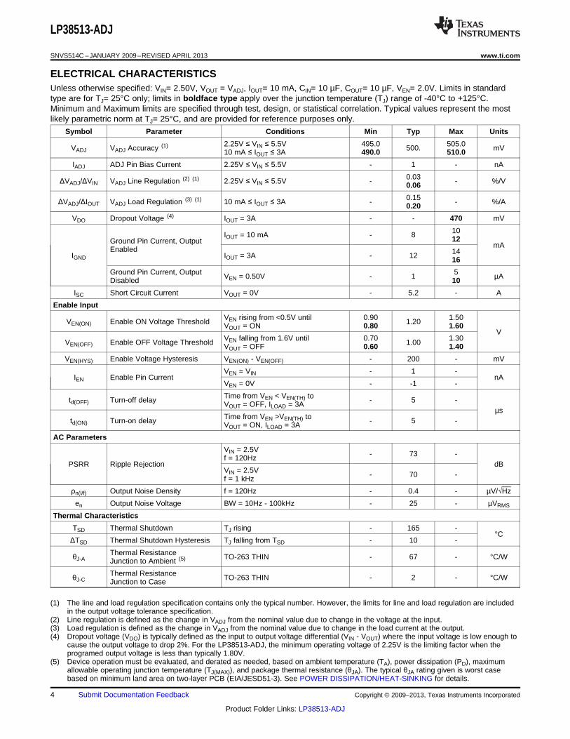
ELECTRICAL CHARACTERISTICSUnless otherwise specified: VIN= 2.50V, VOUT = VADJ, IOUT= 10 mA, CIN= 10 µF, COUT= 10 µF, VEN= 2.0V. Limits in standardtype are for TJ= 25°C only; limits in boldface type apply over the junction temperature (TJ) range of -40°C to +125°C.Minimum and Maximum limits are specified through test, design, or statistical correlation. Typical values represent the mostlikely parametric norm at TJ= 25°C, and are provided for reference purposes only.
Symbol Parameter Conditions Min Typ Max Units
2.25V ≤ VIN ≤ 5.5V 495.0 505.0VADJ VADJ Accuracy (1) 500. mV10 mA ≤ IOUT ≤ 3A 490.0 510.0
IADJ ADJ Pin Bias Current 2.25V ≤ VIN ≤ 5.5V - 1 - nA
0.03ΔVADJ/ΔVIN VADJ Line Regulation (2) (1) 2.25V ≤ VIN ≤ 5.5V - - %/V0.06
0.15ΔVADJ/ΔIOUT VADJ Load Regulation (3) (1) 10 mA ≤ IOUT ≤ 3A - - %/A0.20
VDO Dropout Voltage (4) IOUT = 3A - - 470 mV
10IOUT = 10 mA - 8 12Ground Pin Current, Output mAEnabled 14IGND IOUT = 3A - 12 16
Ground Pin Current, Output 5VEN = 0.50V - 1 µADisabled 10
ISC Short Circuit Current VOUT = 0V - 5.2 - A
Enable Input
VEN rising from <0.5V until 0.90 1.50VEN(ON) Enable ON Voltage Threshold 1.20VOUT = ON 0.80 1.60V
VEN falling from 1.6V until 0.70 1.30VEN(OFF) Enable OFF Voltage Threshold 1.00VOUT = OFF 0.60 1.40
VEN(HYS) Enable Voltage Hysteresis VEN(ON) - VEN(OFF) - 200 - mV
VEN = VIN - 1 -IEN Enable Pin Current nA
VEN = 0V - -1 -
Time from VEN < VEN(TH) totd(OFF) Turn-off delay - 5 -VOUT = OFF, ILOAD = 3Aµs
Time from VEN >VEN(TH) totd(ON) Turn-on delay - 5 -VOUT = ON, ILOAD = 3A
AC Parameters
VIN = 2.5V - 73 -f = 120HzPSRR Ripple Rejection dB
VIN = 2.5V - 70 -f = 1 kHz
ρn(l/f) Output Noise Density f = 120Hz - 0.4 - µV/√Hz
en Output Noise Voltage BW = 10Hz - 100kHz - 25 - µVRMS
Thermal Characteristics
TSD Thermal Shutdown TJ rising - 165 -°C
ΔTSD Thermal Shutdown Hysteresis TJ falling from TSD - 10 -
Thermal ResistanceθJ-A TO-263 THIN - 67 - °C/WJunction to Ambient (5)
Thermal ResistanceθJ-C TO-263 THIN - 2 - °C/WJunction to Case
(1) The line and load regulation specification contains only the typical number. However, the limits for line and load regulation are includedin the output voltage tolerance specification.
(2) Line regulation is defined as the change in VADJ from the nominal value due to change in the voltage at the input.(3) Load regulation is defined as the change in VADJ from the nominal value due to change in the load current at the output.(4) Dropout voltage (VDO) is typically defined as the input to output voltage differential (VIN - VOUT) where the input voltage is low enough to
cause the output voltage to drop 2%. For the LP38513-ADJ, the minimum operating voltage of 2.25V is the limiting factor when theprogramed output voltage is less than typically 1.80V.
(5) Device operation must be evaluated, and derated as needed, based on ambient temperature (TA), power dissipation (PD), maximumallowable operating junction temperature (TJ(MAX)), and package thermal resistance (θJA). The typical θJA rating given is worst casebased on minimum land area on two-layer PCB (EIA/JESD51-3). See POWER DISSIPATION/HEAT-SINKING for details.
4 Submit Documentation Feedback Copyright © 2009–2013, Texas Instruments Incorporated
Product Folder Links: LP38513-ADJ
LP38513-ADJ
www.ti.com SNVS514C –JANUARY 2009–REVISED APRIL 2013
TYPICAL PERFORMANCE CHARACTERISTICSUnless otherwise specified: TJ = 25°C, VIN = 2.50V, VOUT = VADJ, VEN = 2.0V, CIN = 10 µF, COUT = 10 µF, IOUT = 10 mA.
VADJ VOUTvs vs
Temperature VIN
Figure 1. Figure 2.
Ground Pin Current (IGND) Ground Pin Current (IGND)vs vsVIN Temperature
Figure 3. Figure 4.
Ground Pin Current (IGND) Enable Thresholdvs vs
Temperature Temperature
Figure 5. Figure 6.
Copyright © 2009–2013, Texas Instruments Incorporated Submit Documentation Feedback 5
Product Folder Links: LP38513-ADJ
LP38513-ADJ
SNVS514C –JANUARY 2009–REVISED APRIL 2013 www.ti.com
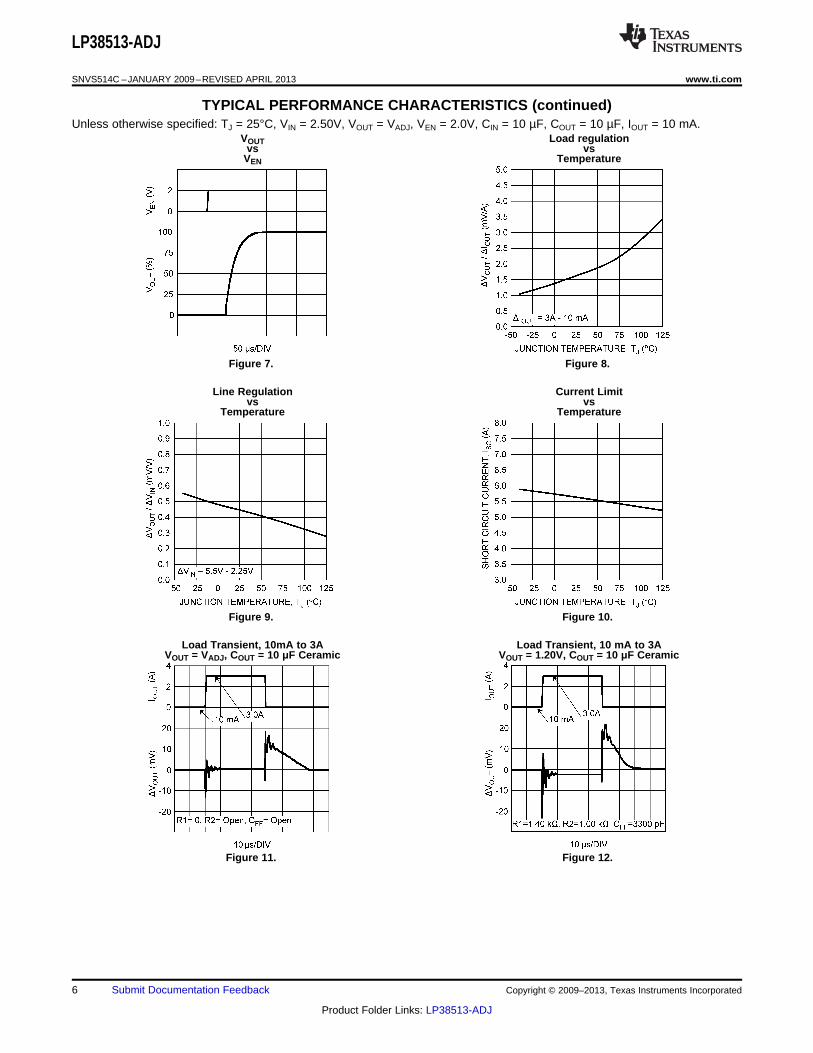
TYPICAL PERFORMANCE CHARACTERISTICS (continued)Unless otherwise specified: TJ = 25°C, VIN = 2.50V, VOUT = VADJ, VEN = 2.0V, CIN = 10 µF, COUT = 10 µF, IOUT = 10 mA.
VOUT Load regulationvs vs
VEN Temperature
Figure 7. Figure 8.
Line Regulation Current Limitvs vs
Temperature Temperature
Figure 9. Figure 10.
Load Transient, 10mA to 3A Load Transient, 10 mA to 3AVOUT = VADJ, COUT = 10 μF Ceramic VOUT = 1.20V, COUT = 10 μF Ceramic
Figure 11. Figure 12.
6 Submit Documentation Feedback Copyright © 2009–2013, Texas Instruments Incorporated
Product Folder Links: LP38513-ADJ
LP38513-ADJ
www.ti.com SNVS514C –JANUARY 2009–REVISED APRIL 2013
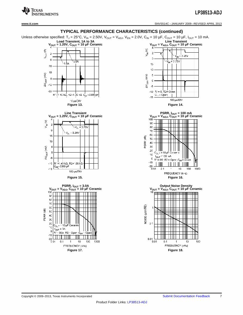
TYPICAL PERFORMANCE CHARACTERISTICS (continued)Unless otherwise specified: TJ = 25°C, VIN = 2.50V, VOUT = VADJ, VEN = 2.0V, CIN = 10 µF, COUT = 10 µF, IOUT = 10 mA.
Load Transient, 1A to 3A Line TransientVOUT = 1.20V, COUT = 10 μF Ceramic VOUT = VADJ, COUT = 10 μF Ceramic
Figure 13. Figure 14.
Line Transient PSRR, IOUT = 100 mAVOUT = 1.20V, COUT = 10 μF Ceramic VOUT = VADJ, COUT = 10 μF Ceramic
Figure 15. Figure 16.
PSRR, IOUT = 3.0A Output Noise DensityVOUT = VADJ, COUT = 10 μF Ceramic VOUT = VADJ, COUT = 10 μF Ceramic
Figure 17. Figure 18.
Copyright © 2009–2013, Texas Instruments Incorporated Submit Documentation Feedback 7
Product Folder Links: LP38513-ADJ
LP38513-ADJ
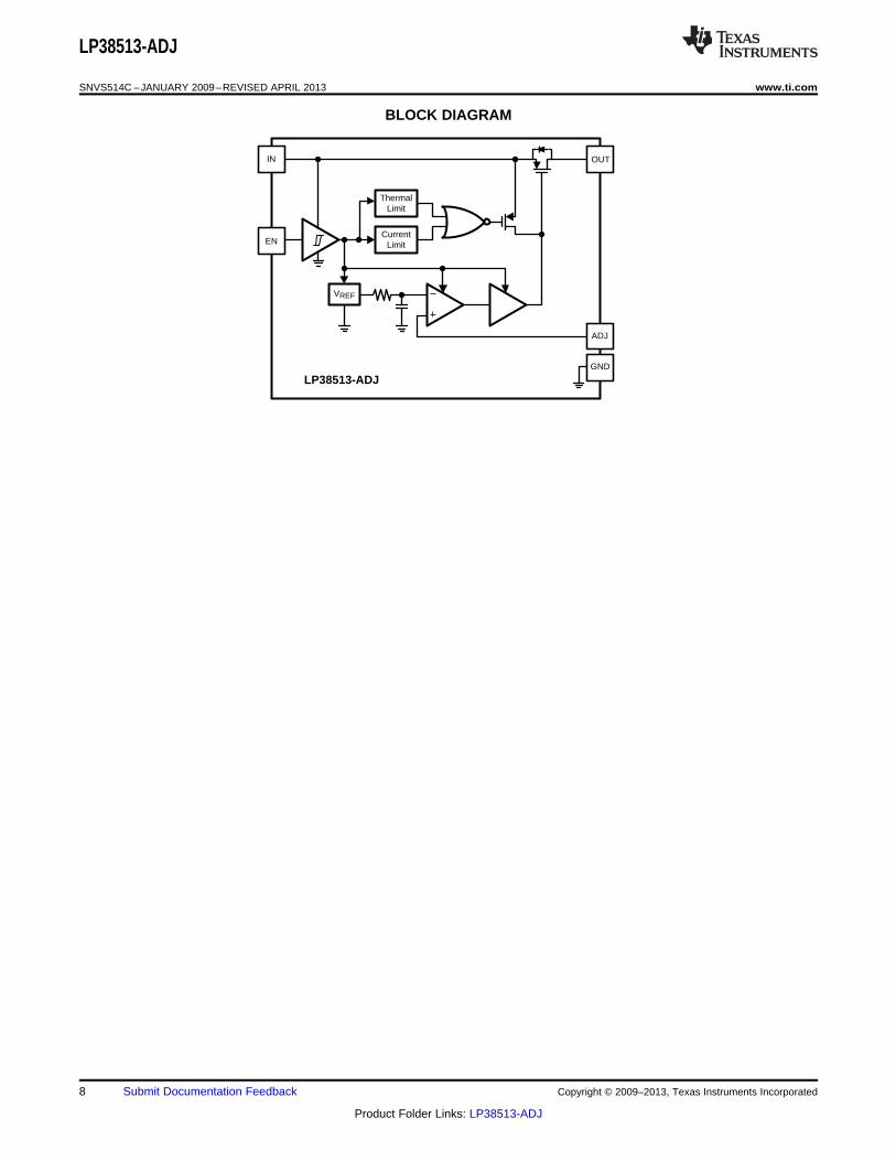
ThermalLimit
CurrentLimit
VREF
ADJ
IN
EN
GND
OUT
LP38513-ADJ
SNVS514C –JANUARY 2009–REVISED APRIL 2013 www.ti.com
BLOCK DIAGRAM
8 Submit Documentation Feedback Copyright © 2009–2013, Texas Instruments Incorporated
Product Folder Links: LP38513-ADJ
LP38513-ADJ
www.ti.com SNVS514C –JANUARY 2009–REVISED APRIL 2013
APPLICATION INFORMATION
EXTERNAL CAPACITORS
Like any low-dropout regulator, external capacitors are required to assure stability. These capacitors must becorrectly selected for proper performance.
Input Capacitor
A ceramic input capacitor of at least 10 µF is required. For general usage across all load currents and operatingconditions, a 10 µF ceramic input capacitor will provide satisfactory performance.
Output Capacitor
A ceramic capacitor with a minimum value of 10 µF is required at the output pin for loop stability. It must belocated less than 1 cm from the device and connected directly to the output and ground pin using traces whichhave no other currents flowing through them. As long as the minimum of 10 µF ceramic is met, there is nolimitation on any additional capacitance.
X7R and X5R dielectric ceramic capacitors are strongly recommended, as they typically maintain a capacitancerange within ±20% of nominal over full operating ratings of temperature and voltage. Of course, they are typicallylarger and more costly than Z5U/Y5U types for a given voltage and capacitance.
Z5U and Y5V dielectric ceramics are not recommended as the capacitance will drop severely with appliedvoltage. A typical Z5U or Y5V capacitor can lose 60% of its rated capacitance with half of the rated voltageapplied to it. The Z5U and Y5V also exhibit a severe temperature effect, losing more than 50% of nominalcapacitance at high and low limits of the temperature range.
Application Information
REVERSE VOLTAGE
A reverse voltage condition will exist when the voltage at the output pin is higher than the voltage at the input pin.Typically this will happen when VIN is abruptly taken low and COUT continues to hold a sufficient charge such thatthe input to output voltage becomes reversed. A less common condition is when an alternate voltage source isconnected to the output.
There are two possible paths for current to flow from the output pin back to the input during a reverse voltagecondition.
While VIN is high enough to keep the control circuity alive, and the Enable pin is above the VEN(ON) threshold, thecontrol circuitry will attempt to regulate the output voltage. Since the input voltage is less than the programmedoutput voltage, the control circuit will drive the gate of the pass element to the full on condition when the outputvoltage begins to fall. In this condition, reverse current will flow from the output pin to the input pin, limited onlyby the RDS(ON) of the pass element and the output to input voltage differential. Discharging an output capacitor upto 1000 µF in this manner will not damage the device as the current will rapidly decay. However, continuousreverse current should be avoided. When the Enable is low this condition will be prevented.
The internal PFET pass element in the LP38513-ADJ has an inherent parasitic diode. During normal operation,the input voltage is higher than the output voltage and the parasitic diode is reverse biased. However, if theoutput voltage to input voltage differential is more than 500 mV (typical) the parasitic diode becomes forwardbiased and current flows from the output pin to the input pin through the diode. The current in the parasitic diodeshould be limited to less than 1A continuous and 5A peak.
If used in a dual-supply system where the regulator output load is returned to a negative supply, the output pinmust be diode clamped to ground. A Schottky diode is recommended for this protective clamp.
SHORT-CIRCUIT PROTECTION
The LP38513-ADJ is short circuit protected, and in the event of a peak over-current condition the short-circuitcontrol loop will rapidly drive the output PMOS pass element off. Once the power pass element shuts down, thecontrol loop will rapidly cycle the output on and off until the average power dissipation causes the thermalshutdown circuit to respond to servo the on/off cycling to a lower frequency. Please refer to the POWERDISSIPATION/HEAT-SINKING section for power dissipation calculations.
Copyright © 2009–2013, Texas Instruments Incorporated Submit Documentation Feedback 9
Product Folder Links: LP38513-ADJ
LP38513-ADJ
SNVS514C –JANUARY 2009–REVISED APRIL 2013 www.ti.com
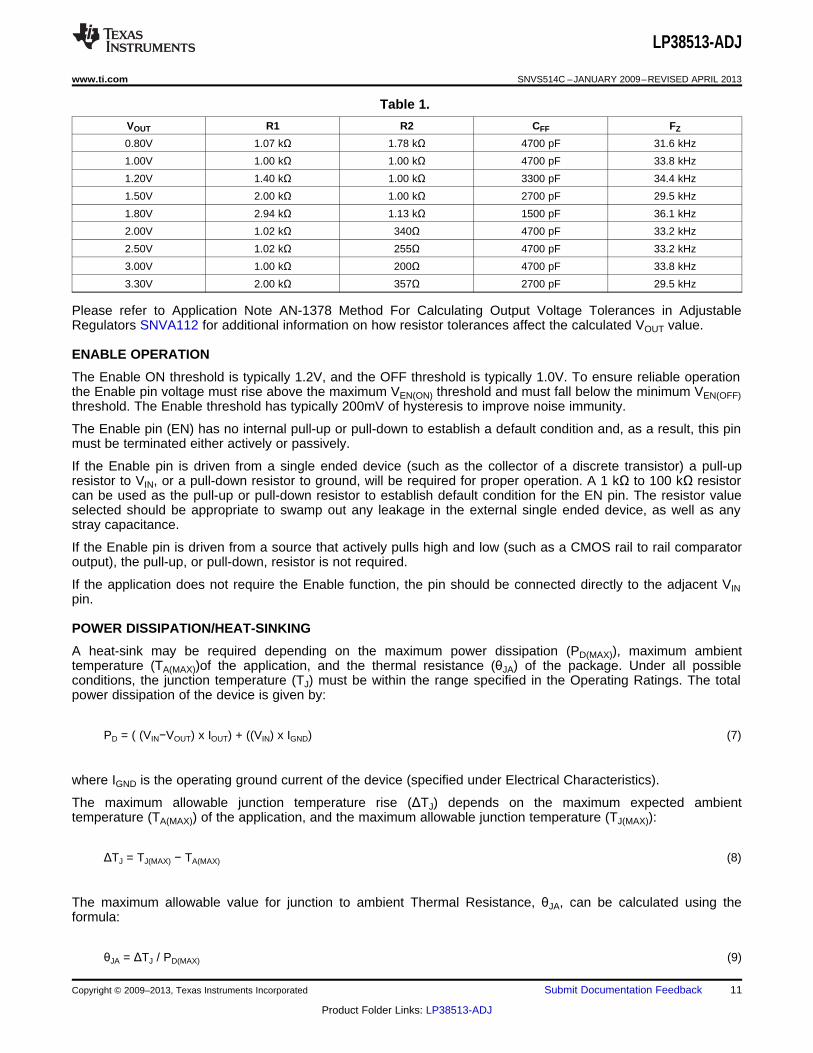
SETTING THE OUTPUT VOLTAGE
The output voltage is set using the external resistive divider R1 and R2. The output voltage is given by theformula:
VOUT = VADJ x (1 + (R1/R2)) (1)
The resistors used for R1 and R2 should be high quality, tight tolerance, and with matching temperaturecoefficients. It is important to remember that, although the value of VADJ is specified, the final value of VOUT isnot. The use of low quality resistors for R1 and R2 can easily produce a VOUT value that is unacceptable.
It is recommended that the values selected for R1 and R2 are such that the parallel value is less than 1.00 kΩ.This is to reduce the possibility of any internal parasitic capacitances on the ADJ pin from creating anundesirable phase shift that may interfere with device stability.
( (R1 x R2) / (R1 + R2) ) ≤ 1.00 kΩ (2)
FEED FORWARD CAPACITOR, CFF
When using a ceramic capacitor for COUT, the typical ESR value will be too small to provide any meaningfulpositive phase compensation, FZ, to offset the internal negative phase shifts in the gain loop.
FZ = 1 / (2 x π x COUT x ESR) (3)
A capacitor placed across the gain resistor R1 will provide additional phase margin to improve load transientresponse of the device. This capacitor, CFF, in parallel with R1, will form a zero in the loop response given by theformula:
FZ = 1 / (2 x π x CFF x R1) (4)
For optimum load transient response select CFF so the zero frequency, FZ, falls between 20 kHz and 40 kHz.
CFF = 1 / (2 x π x R1 x FZ) (5)
The phase lead provided by CFF diminishes as the DC gain approaches unity, or VOUT approaches VADJ. This isbecause CFF also forms a pole with a frequency of:
FP = 1 / (2 x π x CFF x (R1 || R2) ) (6)
It's important to note that at higher output voltages, where R1 is much larger than R2, the pole and zero are farapart in frequency. At lower output voltages the frequency of the pole and the zero mover closer together. Thephase lead provided from CFF diminishes quickly as the output voltage is reduced, and has no effect when VOUT= VADJ. For this reason, relying on this compensation technique alone is adequate only for higher outputvoltages.
Table 1 lists some suggested, best fit, standard ±1% resistor values for R1 and R2, and a standard ±10%capacitor values for CFF, for a range of VOUT values. Other values of R1, R2, and CFF are available that will givesimilar results.
10 Submit Documentation Feedback Copyright © 2009–2013, Texas Instruments Incorporated
Product Folder Links: LP38513-ADJ
LP38513-ADJ
www.ti.com SNVS514C –JANUARY 2009–REVISED APRIL 2013
Table 1.
VOUT R1 R2 CFF FZ
0.80V 1.07 kΩ 1.78 kΩ 4700 pF 31.6 kHz
1.00V 1.00 kΩ 1.00 kΩ 4700 pF 33.8 kHz
1.20V 1.40 kΩ 1.00 kΩ 3300 pF 34.4 kHz
1.50V 2.00 kΩ 1.00 kΩ 2700 pF 29.5 kHz
1.80V 2.94 kΩ 1.13 kΩ 1500 pF 36.1 kHz
2.00V 1.02 kΩ 340Ω 4700 pF 33.2 kHz
2.50V 1.02 kΩ 255Ω 4700 pF 33.2 kHz
3.00V 1.00 kΩ 200Ω 4700 pF 33.8 kHz
3.30V 2.00 kΩ 357Ω 2700 pF 29.5 kHz
Please refer to Application Note AN-1378 Method For Calculating Output Voltage Tolerances in AdjustableRegulators SNVA112 for additional information on how resistor tolerances affect the calculated VOUT value.
ENABLE OPERATION
The Enable ON threshold is typically 1.2V, and the OFF threshold is typically 1.0V. To ensure reliable operationthe Enable pin voltage must rise above the maximum VEN(ON) threshold and must fall below the minimum VEN(OFF)threshold. The Enable threshold has typically 200mV of hysteresis to improve noise immunity.
The Enable pin (EN) has no internal pull-up or pull-down to establish a default condition and, as a result, this pinmust be terminated either actively or passively.
If the Enable pin is driven from a single ended device (such as the collector of a discrete transistor) a pull-upresistor to VIN, or a pull-down resistor to ground, will be required for proper operation. A 1 kΩ to 100 kΩ resistorcan be used as the pull-up or pull-down resistor to establish default condition for the EN pin. The resistor valueselected should be appropriate to swamp out any leakage in the external single ended device, as well as anystray capacitance.
If the Enable pin is driven from a source that actively pulls high and low (such as a CMOS rail to rail comparatoroutput), the pull-up, or pull-down, resistor is not required.
If the application does not require the Enable function, the pin should be connected directly to the adjacent VINpin.
POWER DISSIPATION/HEAT-SINKING
A heat-sink may be required depending on the maximum power dissipation (PD(MAX)), maximum ambienttemperature (TA(MAX))of the application, and the thermal resistance (θJA) of the package. Under all possibleconditions, the junction temperature (TJ) must be within the range specified in the Operating Ratings. The totalpower dissipation of the device is given by:
PD = ( (VIN−VOUT) x IOUT) + ((VIN) x IGND) (7)
where IGND is the operating ground current of the device (specified under Electrical Characteristics).
The maximum allowable junction temperature rise (ΔTJ) depends on the maximum expected ambienttemperature (TA(MAX)) of the application, and the maximum allowable junction temperature (TJ(MAX)):
ΔTJ = TJ(MAX) − TA(MAX) (8)
The maximum allowable value for junction to ambient Thermal Resistance, θJA, can be calculated using theformula:
θJA = ΔTJ / PD(MAX) (9)
Copyright © 2009–2013, Texas Instruments Incorporated Submit Documentation Feedback 11
Product Folder Links: LP38513-ADJ
LP38513-ADJ
SNVS514C –JANUARY 2009–REVISED APRIL 2013 www.ti.com
LP38513-ADJ is available in the TO-263 THIN surface mount package. For a comparison of the TO-263 THINpackage to the standard TO-263 package see Application Note AN-1797 TO-263 THIN Package SNVA328. Thethermal resistance depends on amount of copper area, or heat sink, and on air flow. See Application Note AN-1520 A Guide to Board Layout for Best Thermal Resistance for Exposed Packages SNVA183 for guidelines.
Heat-Sinking the TO-263 THIN Package
The DAP of the TO-263 THIN package is soldered to the copper plane for heat sinking. The TO-263 THINpackage has a θJA rating of 67°C/W, and a θJC rating of 2°C/W. The θJA rating of 67°C/W includes the deviceDAP soldered to an area of 0.055 square inches (0.22 in x 0.25 in) of 1 ounce copper on a two sided PCB, withno airflow. See JEDEC standard EIA/JESD51-3 for more information.
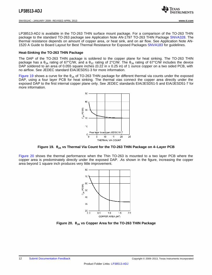
Figure 19 shows a curve for the θJA of TO-263 THIN package for different thermal via counts under the exposedDAP, using a four layer PCB for heat sinking. The thermal vias connect the copper area directly under theexposed DAP to the first internal copper plane only. See JEDEC standards EIA/JESD51-5 and EIA/JESD51-7 formore information.
Figure 19. θJA vs Thermal Via Count for the TO-263 THIN Package on 4–Layer PCB
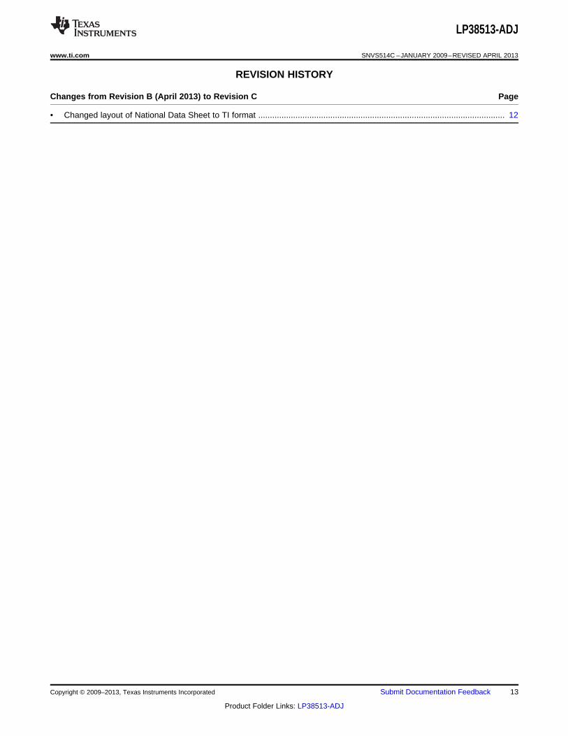
Figure 20 shows the thermal performance when the Thin TO-263 is mounted to a two layer PCB where thecopper area is predominately directly under the exposed DAP. .As shown in the figure, increasing the copperarea beyond 1 square inch produces very little improvement.
Figure 20. θJA vs Copper Area for the TO-263 THIN Package
12 Submit Documentation Feedback Copyright © 2009–2013, Texas Instruments Incorporated
Product Folder Links: LP38513-ADJ
LP38513-ADJ
www.ti.com SNVS514C –JANUARY 2009–REVISED APRIL 2013
REVISION HISTORY
Changes from Revision B (April 2013) to Revision C Page
• Changed layout of National Data Sheet to TI format .......................................................................................................... 12
Copyright © 2009–2013, Texas Instruments Incorporated Submit Documentation Feedback 13
Product Folder Links: LP38513-ADJ
PACKAGE OPTION ADDENDUM
www.ti.com 21-May-2013
Addendum-Page 1
PACKAGING INFORMATION
Orderable Device Status(1)
Package Type PackageDrawing
Pins PackageQty
Eco Plan(2)
Lead/Ball Finish MSL Peak Temp(3)
Op Temp (°C) Device Marking(4/5)
Samples
LP38513TJ-ADJ/NOPB ACTIVE TO-263 NDQ 5 1000 Green (RoHS& no Sb/Br)
CU SN Level-1-260C-UNLIM -40 to 125 LP38513TJ-ADJ
(1) The marketing status values are defined as follows:ACTIVE: Product device recommended for new designs.LIFEBUY: TI has announced that the device will be discontinued, and a lifetime-buy period is in effect.NRND: Not recommended for new designs. Device is in production to support existing customers, but TI does not recommend using this part in a new design.PREVIEW: Device has been announced but is not in production. Samples may or may not be available.OBSOLETE: TI has discontinued the production of the device.
(2) Eco Plan - The planned eco-friendly classification: Pb-Free (RoHS), Pb-Free (RoHS Exempt), or Green (RoHS & no Sb/Br) - please check http://www.ti.com/productcontent for the latest availabilityinformation and additional product content details.TBD: The Pb-Free/Green conversion plan has not been defined.Pb-Free (RoHS): TI's terms "Lead-Free" or "Pb-Free" mean semiconductor products that are compatible with the current RoHS requirements for all 6 substances, including the requirement thatlead not exceed 0.1% by weight in homogeneous materials. Where designed to be soldered at high temperatures, TI Pb-Free products are suitable for use in specified lead-free processes.Pb-Free (RoHS Exempt): This component has a RoHS exemption for either 1) lead-based flip-chip solder bumps used between the die and package, or 2) lead-based die adhesive used betweenthe die and leadframe. The component is otherwise considered Pb-Free (RoHS compatible) as defined above.Green (RoHS & no Sb/Br): TI defines "Green" to mean Pb-Free (RoHS compatible), and free of Bromine (Br) and Antimony (Sb) based flame retardants (Br or Sb do not exceed 0.1% by weightin homogeneous material)
(3) MSL, Peak Temp. -- The Moisture Sensitivity Level rating according to the JEDEC industry standard classifications, and peak solder temperature.
(4) There may be additional marking, which relates to the logo, the lot trace code information, or the environmental category on the device.
(5) Multiple Device Markings will be inside parentheses. Only one Device Marking contained in parentheses and separated by a "~" will appear on a device. If a line is indented then it is a continuationof the previous line and the two combined represent the entire Device Marking for that device.
Important Information and Disclaimer:The information provided on this page represents TI's knowledge and belief as of the date that it is provided. TI bases its knowledge and belief on informationprovided by third parties, and makes no representation or warranty as to the accuracy of such information. Efforts are underway to better integrate information from third parties. TI has taken andcontinues to take reasonable steps to provide representative and accurate information but may not have conducted destructive testing or chemical analysis on incoming materials and chemicals.TI and TI suppliers consider certain information to be proprietary, and thus CAS numbers and other limited information may not be available for release.
In no event shall TI's liability arising out of such information exceed the total purchase price of the TI part(s) at issue in this document sold by TI to Customer on an annual basis.
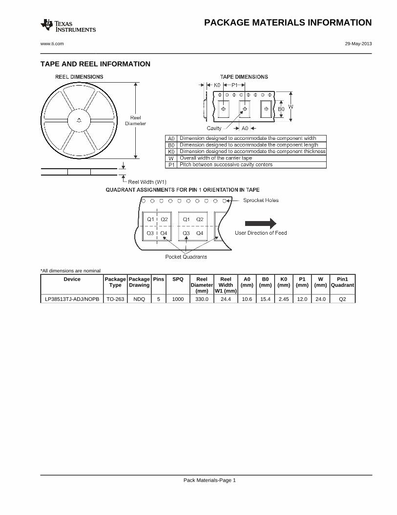
TAPE AND REEL INFORMATION
*All dimensions are nominal
Device PackageType
PackageDrawing
Pins SPQ ReelDiameter
(mm)
ReelWidth
W1 (mm)
A0(mm)
B0(mm)
K0(mm)
P1(mm)
W(mm)
Pin1Quadrant
LP38513TJ-ADJ/NOPB TO-263 NDQ 5 1000 330.0 24.4 10.6 15.4 2.45 12.0 24.0 Q2
PACKAGE MATERIALS INFORMATION
www.ti.com 29-May-2013
Pack Materials-Page 1
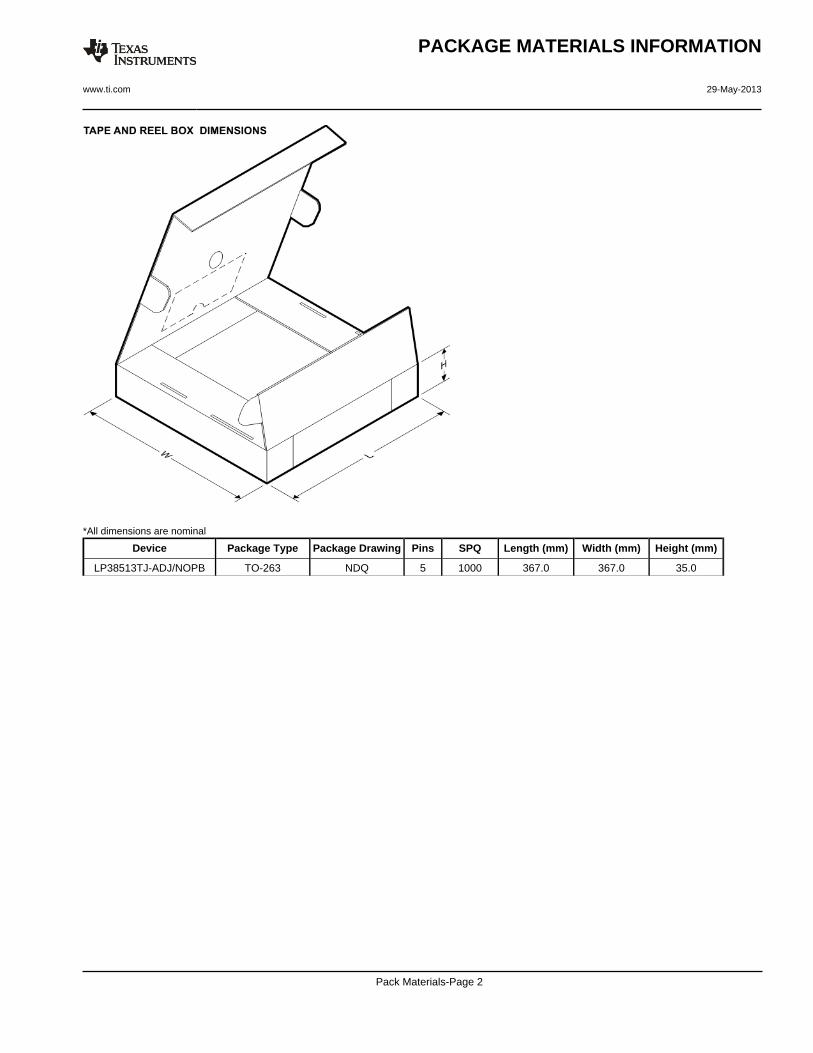
*All dimensions are nominal
Device Package Type Package Drawing Pins SPQ Length (mm) Width (mm) Height (mm)
LP38513TJ-ADJ/NOPB TO-263 NDQ 5 1000 367.0 367.0 35.0
PACKAGE MATERIALS INFORMATION
www.ti.com 29-May-2013
Pack Materials-Page 2
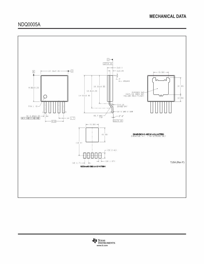
MECHANICAL DATA
NDQ0005A
www.ti.com
TJ5A (Rev F)
IMPORTANT NOTICE
Texas Instruments Incorporated and its subsidiaries (TI) reserve the right to make corrections, enhancements, improvements and otherchanges to its semiconductor products and services per JESD46, latest issue, and to discontinue any product or service per JESD48, latestissue. Buyers should obtain the latest relevant information before placing orders and should verify that such information is current andcomplete. All semiconductor products (also referred to herein as “components”) are sold subject to TI’s terms and conditions of salesupplied at the time of order acknowledgment.
TI warrants performance of its components to the specifications applicable at the time of sale, in accordance with the warranty in TI’s termsand conditions of sale of semiconductor products. Testing and other quality control techniques are used to the extent TI deems necessaryto support this warranty. Except where mandated by applicable law, testing of all parameters of each component is not necessarilyperformed.
TI assumes no liability for applications assistance or the design of Buyers’ products. Buyers are responsible for their products andapplications using TI components. To minimize the risks associated with Buyers’ products and applications, Buyers should provideadequate design and operating safeguards.
TI does not warrant or represent that any license, either express or implied, is granted under any patent right, copyright, mask work right, orother intellectual property right relating to any combination, machine, or process in which TI components or services are used. Informationpublished by TI regarding third-party products or services does not constitute a license to use such products or services or a warranty orendorsement thereof. Use of such information may require a license from a third party under the patents or other intellectual property of thethird party, or a license from TI under the patents or other intellectual property of TI.
Reproduction of significant portions of TI information in TI data books or data sheets is permissible only if reproduction is without alterationand is accompanied by all associated warranties, conditions, limitations, and notices. TI is not responsible or liable for such altereddocumentation. Information of third parties may be subject to additional restrictions.
Resale of TI components or services with statements different from or beyond the parameters stated by TI for that component or servicevoids all express and any implied warranties for the associated TI component or service and is an unfair and deceptive business practice.TI is not responsible or liable for any such statements.
Buyer acknowledges and agrees that it is solely responsible for compliance with all legal, regulatory and safety-related requirementsconcerning its products, and any use of TI components in its applications, notwithstanding any applications-related information or supportthat may be provided by TI. Buyer represents and agrees that it has all the necessary expertise to create and implement safeguards whichanticipate dangerous consequences of failures, monitor failures and their consequences, lessen the likelihood of failures that might causeharm and take appropriate remedial actions. Buyer will fully indemnify TI and its representatives against any damages arising out of the useof any TI components in safety-critical applications.
In some cases, TI components may be promoted specifically to facilitate safety-related applications. With such components, TI’s goal is tohelp enable customers to design and create their own end-product solutions that meet applicable functional safety standards andrequirements. Nonetheless, such components are subject to these terms.
No TI components are authorized for use in FDA Class III (or similar life-critical medical equipment) unless authorized officers of the partieshave executed a special agreement specifically governing such use.
Only those TI components which TI has specifically designated as military grade or “enhanced plastic” are designed and intended for use inmilitary/aerospace applications or environments. Buyer acknowledges and agrees that any military or aerospace use of TI componentswhich have not been so designated is solely at the Buyer's risk, and that Buyer is solely responsible for compliance with all legal andregulatory requirements in connection with such use.
TI has specifically designated certain components as meeting ISO/TS16949 requirements, mainly for automotive use. In any case of use ofnon-designated products, TI will not be responsible for any failure to meet ISO/TS16949.
Products Applications
Audio www.ti.com/audio Automotive and Transportation www.ti.com/automotive
Amplifiers amplifier.ti.com Communications and Telecom www.ti.com/communications
Data Converters dataconverter.ti.com Computers and Peripherals www.ti.com/computers
DLP® Products www.dlp.com Consumer Electronics www.ti.com/consumer-apps
DSP dsp.ti.com Energy and Lighting www.ti.com/energy
Clocks and Timers www.ti.com/clocks Industrial www.ti.com/industrial
Interface interface.ti.com Medical www.ti.com/medical
Logic logic.ti.com Security www.ti.com/security
Power Mgmt power.ti.com Space, Avionics and Defense www.ti.com/space-avionics-defense
Microcontrollers microcontroller.ti.com Video and Imaging www.ti.com/video
RFID www.ti-rfid.com
OMAP Applications Processors www.ti.com/omap TI E2E Community e2e.ti.com
Wireless Connectivity www.ti.com/wirelessconnectivity
Mailing Address: Texas Instruments, Post Office Box 655303, Dallas, Texas 75265Copyright © 2013, Texas Instruments Incorporated