Embed Size (px)
Citation preview
CACHE MEMORY MODEL FOR CYCLE ACCURATE
SIMULATION
By
RANGANATHAN SRIDHARAN
Bachelor of Engineering in Electronics & Communications
University of Madras
Chennai, Tamilnadu
2003
Submitted to the Faculty of the
Graduate College of the
Oklahoma State University
in partial fulfillment of
the requirements for
the Degree of
MASTER OF SCIENCE
December, 2007
ii
CACHE MEMORY MODEL FOR CYCLE
ACCURATE SIMULATION
Thesis Approved:
Dr. Louis G. Johnson
Thesis Adviser
Dr. Sohum Sohoni
Committee Member Name Here
Dr. Rama Ramakumar
Committee Member Name Here
A. Gordon Emslie
Dean of the Graduate College
iii
ACKNOWLEDGEMENT
First, I would like to thank my advisor and committee chair Dr. Louis G. Johnson
for having stood by me patiently for such a long time and guiding me in the right
direction. I would also like to thank my committee members Dr. Sohum Sohoni and Dr.
Rama Ramakumar for their valuable advice and guidance on features required for a good
cache simulator.
I would like to thank Dr. Jong Moon Chung and Dr. Chriswell Hutchens for their
guidance and financial support without which my stay at OSU would not have been
possible. I would also like to thank Aswin Ramachandran, Micro architecture Lab, OSU
for helping me in integration of my cache model with his processor model and also for
his valuable suggestions whenever I got stuck. I would also like to thank all the members
of MSVLSI (Mixed-Signal VLSI) lab, Dr.Liu, Usha, Vijay, Srinivasan, Henry and
Dr.Hooi Miin Soo for helping me in all ways during this long stay at OSU. Without them
my life would have been uninteresting and uneventful.
I would like to thank my parents and my sister for their constant encouragement,
motivation and for having believed in me till the end. To all of them I dedicate this work.
iv
TABLE OF CONTENTS
Chapter Page
CHAPTER 1 ....................................................................................................................... 9
INTRODUCTION .............................................................................................................. 9
1.0 Thesis Introduction............................................................................................. 10
1.1 Motivation .......................................................................................................... 12
1.2 Thesis Organization............................................................................................ 13
CHAPTER 2 ..................................................................................................................... 14
MEMORY HIERARCHY: CACHE OVERVIEW .......................................................... 14
2.0 Memory Hierarchy ............................................................................................. 15
2.1 Memory implementation .................................................................................... 21
CHAPTER 3 ..................................................................................................................... 24
CACHE ORGANIZATION.............................................................................................. 24
3.0 Cache Terminology.............................................Error! Bookmark not defined.
3.1 Cache Types Based on Block Placement ........................................................... 24
3.1.1 Direct-mapped Cache.................................................................................. 25
3.1.2 Fully-associative cache ............................................................................... 27
3.1.3 N-way associative cache ............................................................................. 27
3.2 Cache Replacement Algorithms......................................................................... 28
3.3 Cache-Memory Interaction ................................................................................ 30
3.4 Cache Performance Metrics ............................................................................... 32
3.4.1 Cache Miss Types ....................................................................................... 33
v
3.5 Cache Addressing............................................................................................... 35
3.6 Cache hierarchy.................................................................................................. 36
3.7 Cache coherency algorithms for multi-ported and multi-processor environments
37
3.8 Latency and bandwidth ...................................................................................... 39
3.9 Cache Modeling ................................................................................................. 40
CHAPTER 4 ..................................................................................................................... 42
IMPLEMENTATION OF THE CACHE MODEL .......................................................... 42
4.0 Introduction ........................................................................................................ 42
4.1 Cache Controller Implementation ...................................................................... 43
4.2 Replacement Controller...................................................................................... 48
4.3 Constraints in Current Design ............................................................................ 49
4.4 Implementation Issues on a sequential Processor .............................................. 50
CHAPTER 5 ..................................................................................................................... 54
SUMMARY AND CONCLUDING REMARKS ............................................................ 54
5.0 Results ................................................................................................................ 54
5.0.1 Simulation of a single level instruction cache with linear pipeline ............ 55
5.0.2 Simulation results for two level instruction caches with linear pipeline .... 55
5.0.3 Simulation of four-issue cache for four-wide superscalar .......................... 57
5.0.4 Measurement of Average Throughput and Cache Histogram .................... 58
5.0.5 Measurement of Average Latency .............................................................. 61
5.1 Conclusion.......................................................................................................... 63
5.2 Future Work ....................................................................................................... 64

vi
vii
LIST OF TABLES
Table Page
Table 3.1 Mapping function comparison table ................................................................. 27
viii
LIST OF FIGURES
Figure Page
Figure 1-1 Logic and memory performance gap .............................................................. 10
Figure 2-1 Memory hierarchy showing the trend in speed and size going down the
hierarchy with possible implementations for each level of memory ................................ 16
Figure 2-2 Various cache architectures for multi-core systems [11]................................ 18
Figure 2-3 Typical Memory Hierarchy of a modern day computer [11] .......................... 20
Figure 3.3-1 The caches in the DECStation 3100 each contain 16K blocks with one word
per block [1]...................................................................................................................... 26
Figure 3.3-2 Four-way set associative cache with four comparators and a 4-to-1 mux [1]
........................................................................................................................................... 28
Figure 3-3 Cache Coherent System .................................................................................. 38
Figure 3-4 Cache Model: Mapping Architecture and Application [8] ............................. 40
Figure 4-1 Block Diagram of the Cache Controller.......................................................... 44
Figure 4-2Hash based fast indexing for most common cases........................................... 52
Figure 4-3 Hash indexing for a fully associative cache.................................................... 53
Figure 5-1 Linear Pipeline Level-1 Instruction Cache Performance ................................ 56
Figure 5-2 Linear Pipeline Level-2 Instruction Cache Performance ................................ 57
Figure 5-3 Performance of a 1K 4-way cache for a four-issue out-of-order processor .... 58
Figure 5-4 Histogram of Cache hits to every set for mcf2006 ......................................... 60
Figure 5-5 Modifications for performing average latency calculation ............................. 62
Figure 5-6 Modifications for a prefetch performance measurement ................................ 65

9
CHAPTER 1
INTRODUCTION
Over the years, major technological advancements and innovations in the way computers
operate took us through several generations of computers with each conveying a leap
beyond existing machines. The sustained improvements in the fundamental computer
architecture are leading to increasingly smaller, cheaper, more powerful, more efficient
and reliable devices every day. In the first four generations of computers, if the focus had
been on increasing the number of logic elements in a single CPU, the current generation
is focused on higher calculation performance using massive parallelism and ever
improving architecture and organization.
As high performance superscalar processor organizations are divided into memory access
and instruction execution mechanisms, improvement in processor performance (clock
speed of the operation being the metric in measuring computer’s performance) with no
disparity with memory access speed would result in better overall computer system
performance. But, over the years there are 55% more transistors every year on a single
chip that proportionally increase the speed of CPU as compared to only a 7% increase in
the speed of memory. Always there is this motivating processor – memory performance
gap (depicted in the figure 1.1 below) existing with the bottleneck of relatively slow
memory which is posing a greater challenge for memory designers to come up with a
range of techniques to reduce average memory access time and architectures supporting
out-of-order and speculative execution.
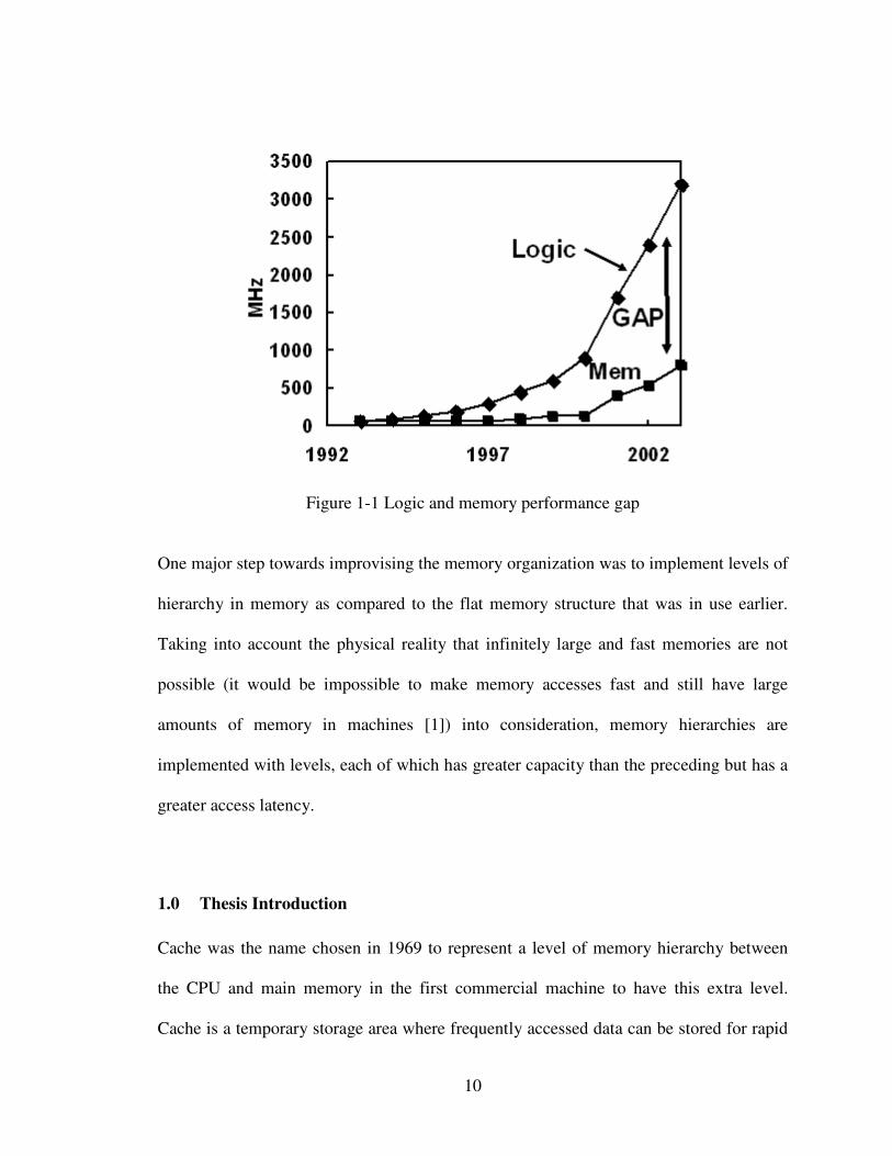
10
Figure 1-1 Logic and memory performance gap
One major step towards improvising the memory organization was to implement levels of
hierarchy in memory as compared to the flat memory structure that was in use earlier.
Taking into account the physical reality that infinitely large and fast memories are not
possible (it would be impossible to make memory accesses fast and still have large
amounts of memory in machines [1]) into consideration, memory hierarchies are
implemented with levels, each of which has greater capacity than the preceding but has a
greater access latency.
1.0 Thesis Introduction
Cache was the name chosen in 1969 to represent a level of memory hierarchy between
the CPU and main memory in the first commercial machine to have this extra level.
Cache is a temporary storage area where frequently accessed data can be stored for rapid
11
access. Once the data is stored in the cache, future access can be made to the cached copy
rather than re-fetching or recomputing the original data, so the average access time is
shorter. Caches have proven to be extremely effective in many areas of computing
because access patterns in typical computer applications have locality of reference. There
are numerous cache architecture and organization schemes that exist and there is scope
for new ones that can be explored for providing as much information as possible, as
required by a CPU with faster access times. The work presented here as a part of my
research is aimed at facilitating cache designers with the ability to simulate and
characterize the performance of cache memory before implementing it in hardware.
An architecture level behavioral model for evaluating the performance of cache in terms
of average access latencies, miss rates and other miss penalties that are accurate at the
cycle level without being too detailed to reduce simulation performance has been
developed in C++. The cache statistics generated assist the designer in selecting an
appropriate cache block size, associativity, replacement policy and other architecture-
level design features. The cache controller implemented here has only 4 states (memory
read, memory write, cache read and cache write) with each stage having variable latency.
All other states that are internal to a regular cache controller are not implemented as the
primary focus is on the interface of the cache with processor and memory thus giving far
better performance with regard to number of simulation cycles consumed.
12
1.1 Motivation
The main motivation for development of such a model was the unavailability of proper
cache models that are fast (the internal details need not be detailed enough to mimic
exactly a cache controller) and at the same time are modular such that several types of
architectures could be easily modified and performance evaluated. Cache size, number of
cache levels in the memory hierarchy and cache policy design are hot topics in the
current period which is a highly unexplored field with each processor having a different
size and varying levels of cache and each application running on a processor behaving
differently on different cache architectures. The entry of multi-core processors introduces
another hurdle where several designs and architectures for the cache need to be explored
so that the various cores can run parallel threads without too much bus communication
overhead. For example, if you look at the current market, two of the industry giants in
processor design, Intel and AMD, don’t agree on a single architecture for their dual-core
and quad-core processors. While Intel wants to stay with a shared L2 cache at least for its
latest iteration [15], AMD with its quad-core architecture wants a dedicated L2 cache and
a shared L3 cache [14]. Similarly there are several multi-core microcontrollers that are
being developed by ARM and IBM that are exploring the use of a shared cache among
the cores. This is also a big need in the field of game console design where multiple
processor cores and multiple GPU cores compete on sharing the data at the fastest
possible rate so that high frame rendering rates could be achieved. Developing cache
models such as these would help us evaluate the performance of various alternatives
across several benchmarks without the need for design time and silicon spins for all
different architectures to be evaluated.

13
1.2 Thesis Organization
This thesis consists of 5 chapters. Chapter 2 gives more details regarding the memory
organization, processor communication with different levels of memory and briefly
describes how level of memory is implemented along with the advantages and limitations
of them. Chapter 3 deals with cache architecture and organization and gives in depth
detail about the crucial factors that dictate the cache performance. Chapter 4 talks about
the simulation methodology developed as a part of this work to evaluate the performance
of cache. Chapter 5 summarizes results of this work in terms of its simulation robustness
and gives details regarding scope of further work.

14
CHAPTER 2
MEMORY HIERARCHY: CACHE OVERVIEW
CPUs today are much more sophisticated with increased operating frequencies.
Frequency of the memory bus and the performance of RAM chips have not increased
proportionally making memory a performance bottleneck. An ideal memory system
would be the one that provides any datum required by the CPU immediately.
Implementation of this ideal memory would not be possible in practise, since memory
design is a fundamental trade-off between capacity, speed and cost. An economic
solution for memory, aimed towards achieving cost as low as the cheapest memory and
speeds as fast as the fastest memory, is to implement memory in a hierarchical manner.
Smaller memories are relatively faster than larger memories built on similar technologies
because larger memories have more delay in signal path (due to added capacitance from
transistors and wires) and also require more levels to decode addresses. Also in most
technologies, smaller memories are faster than larger memories since more memory
power per memory cell can be afforded in smaller designs as compared to larger ones.
Thus, implementing memory in a hierarchy as compared to using large amounts of faster
memory provides more capacity for the same price with only slightly reduced combined
performance.
15
Hierarchical implementation of memory is based on the ‘principle of locality’ that is
exhibited by programs. Temporal locality means that there is a high possibility that the
recently accessed data will be accessed again in the near future. The principle of spatial
locality states that if an item is referenced, items whose addresses are close by will tend
to be referenced soon. Programs are considered to be exhibiting spatial locality since
instructions are normally accessed sequentially with programs showing high spatial
locality thereby making data accesses also to exhibit high spatial locality. Programs are
also considered to be exhibiting temporal locality since programs contain loops with data
likely to be accessed repeatedly resulting in high amounts of temporal locality.
Superscalar processor organizations that by nature divide into instruction fetch
mechanisms and instruction execute mechanisms employ aggressive techniques to exploit
instruction level parallelism (ILP). Those techniques include using wide dispatch and
issue paths for increasing ‘instruction throughput’, using large issue buffers for providing
more instructions in parallel to instruction execution engine, enabling concurrent
execution of instruction by employing parallel functional units and speculating multiple
branches for supplying a continuous instruction stream to the execution engine. In
benefiting the most out of these ILP techniques, instruction fetch bandwidth and latency
are a major concern.
2.0 Memory Hierarchy
The number of levels in the memory hierarchy differs for different architectures. The
fastest memories are more expensive per bit than the slower memories and thus are
16
usually smaller. The price difference arises because of the difference in the capacity
among different implementations for the same amount of silicon. A typical memory
hierarchy for optimal performance is implemented in different levels with each level
having higher speed, smaller size and lower latency closer to the processor than lower
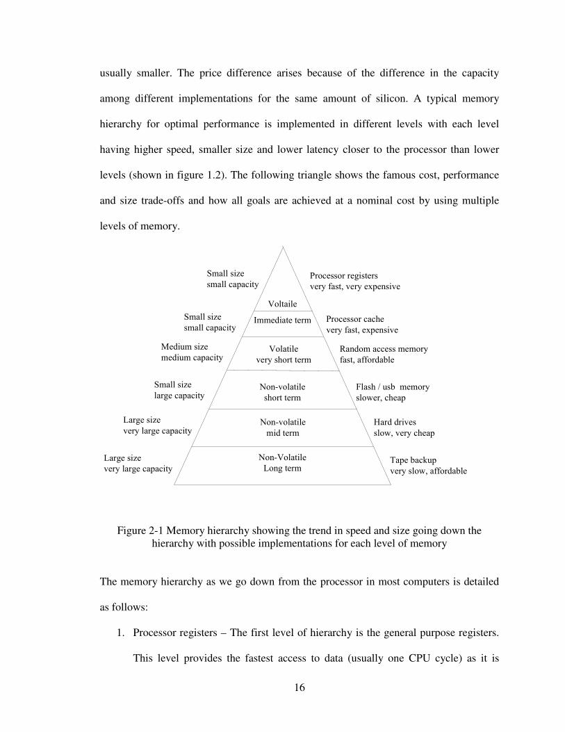
levels (shown in figure 1.2). The following triangle shows the famous cost, performance
and size trade-offs and how all goals are achieved at a nominal cost by using multiple
levels of memory.
Voltaile
Immediate term
Volatile
very short term
Non-volatile
short term
Non-volatile
mid term
Non-Volatile
Long term
Processor registers
very fast, very expensive
Processor cache
very fast, expensive
Random access memory
fast, affordable
Flash / usb memory
slower, cheap
Hard drives
slow, very cheap
Tape backup
very slow, affordable
Small size
small capacity
Small size
small capacity
Medium size
medium capacity
Small size
large capacity
Large size
very large capacity
Large size
very large capacity
Figure 2-1 Memory hierarchy showing the trend in speed and size going down the
hierarchy with possible implementations for each level of memory
The memory hierarchy as we go down from the processor in most computers is detailed
as follows:
1. Processor registers – The first level of hierarchy is the general purpose registers.
This level provides the fastest access to data (usually one CPU cycle) as it is
17
designed as a part of the processor core. Registers are very expensive to
implement and thus is the smallest memory object of all (usually a few hundred
bytes). It is not possible to expand this memory as this is fixed in the CPU.
Registers unquestionably provide fast access since they are part of the execution
datapath itslef. Usually these registers are allocated by the compiler to the parts of
programs where data is repetitively used, like in for-loops in counters.
2. Cache – The next highest performing level in the memory hierarchy is cache.
Cache is usually implemented in different levels (hierarchy of cache) with up to
three levels in the recent architectures. Level 1 (L1) cache is a non-expandable
memory with a size of a few tens of Kbytes. It is often accessed in a few cycles
and costs much less than registers. Instructions requiring memory accesses are
slower than those requiring register accesses owing to the fact that if the data
needed for the execution is not present in L1 cache, the cache controller needs to
look in the L2 cache or, in the worst case, on disk in the virtual memory
subsystem. Level 2 (L2) cache is an optional level of memory. L2 cache is present
as part of the CPU package for some processors like Pentium II and III processors
but sometimes it is not incorporated as a part of CPU like in Intel Celeron
processors. It is usually expandable when it is not in the CPU package. L2 is less
expensive than L1 cache owing to relatively higher latencies but among L2
caches, external ones are more expensive than the ones that are part of CPU
package. Accessing L2 cache is always slower than that of L1 cache by atleast
one cycle (perhaps more, and more so if the L2 cache is not packaged with the
CPU) because most of one memory access cycle is spent to determine that the
18
data it is seeking is not present in the L1 cache. L2 caches are also made slower
than L1 caches to make them inexpensive. Also L2 cache tends to be slower than
L1 cache since it is larger.
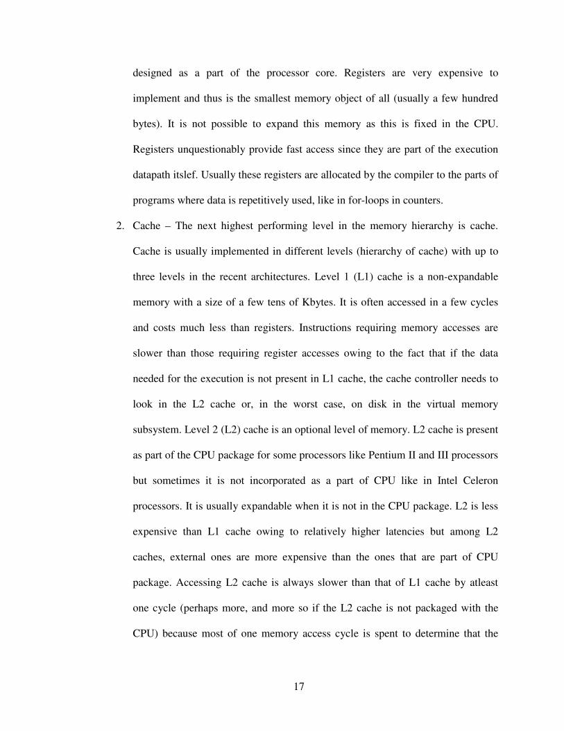
Based on the type of the data stored, there are instruction caches and data caches.
Usually instruction cache and data cache are separate in L1 cache and they are not
separate in level 2 or level 3 (unified cache for L2 an L3). In multi-processor
architectures, cache is shared among the processors. Not all levels are shared for a
multi-processor system but moving the level that is shared closer to the processor
makes cache faster but is too complex and is expensive, whereas moving it to the
bottom makes the processor go through all the levels above it to talk to the next
processor (which makes it slower).
Figure 2-2 Various cache architectures for multi-core systems [11]
3. Main memory – After cache in the memory hierarchy comes main memory. This
is the general-purpose, relatively low-cost memory found in most computer
systems. Typically, this is DRAM or some similar inexpensive memory
technology. Main memory access may take hundreds of clock cycles, but can be
of multiple gigabytes. The amount of data that the system fetches is higher (in
19
blocks) from main memory when L2 - cache miss occurs than the amount of data
fetched from L1 or L2 cache on a hit. This is how the system is designed to make
the adjacent access times faster hoping that spatial locality exists in the system.
This reduces the latency for main memory; however this latency is incurred if the
program does not access data adjacent to the currently accessed one.
4. Virtual memory which comes in the next level of hierarchy is not a real memory
but is a computer system technique that gives an application program the
impression that it has contiguous working memory while in fact it is physically
fragmented and may even overflow on to disk storage. This technique makes
more efficient use of real physical memory and makes programming of large
applications easier. It employs techniques like overlaying, swapping programs
and their data completely out to disk while they are inactive and simulating the
storage on a disk drive as main memory.
5. After the virtual memory comes file storage or shared memory blocks provided by
other peripherals like video display cards. Though disk drives are a lot slower
than main memory, they are very inexpensive and make it conceivable to have
large amounts of data stored on disk drives.
The typical memory hierarchy architecture of a modern day processor hierarchy is shown
below.
20
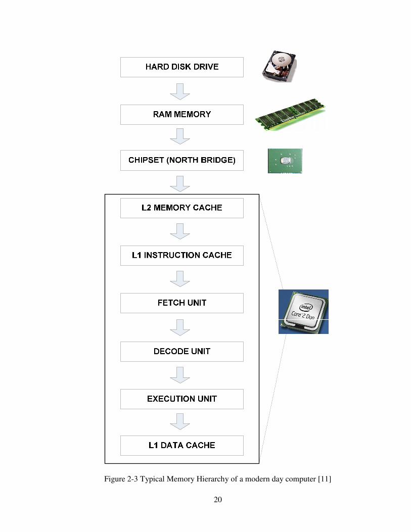
Figure 2-3 Typical Memory Hierarchy of a modern day computer [11]
21
2.1 Memory implementation
Basic principles behind implementation of different kinds of memory are stated in this
section with a more detailed description on cache memory system. A register file is
implemented as an array of registers built from D flip-flops with a decoder for each read
or write port. Reading a register is slightly easier as compared to a write operation as read
operation do not have to change the contents. For performing a read operation, only one
input to select the designated register is required. For a write, along with the register
number, the data to be written as well as the clock input are given as inputs. Read and
write operations cannot be performed simultaneously since that read operation returns the
value from earlier clock cycle while current data is still being written at the clock edge.
SRAM:
Typically caches are built using SRAMs (static random access memories). SRAMs are
memory arrays with a single access port capable of providing either a read or a write with
fixed read access time and fixed write access time to any datum. SRAM has a
configuration in terms of the number of addressable locations it has and width of each
addressable location. A chip select signal must be made active to initiate a read or write
access. For a read operation, instead of using a multiplexer for selecting the designated
register, tri-state buffers are used for each bit (incorporated into the circuitry of basic
SRAM cell) with all the outputs connected to a shared line called a ‘bit line’. This makes
it a more efficient implementation than a large centralized multiplexer [1]. An output
enable determines which cell drives the bus. The design still needs a decoder for
generating an output enable signal and organizing memory as rectangular arrays which

22
can be decoded in two stages. For writes, data to be written, the designated address and
the write enable signals are to be supplied to the SRAM circuitry. The write enable signal
has to be long enough to allow for set-up times and hold times. Synchronous SRAMs are
capable of transferring a block of data from a series of sequential addresses within an
array or row and this makes them a natural choice for building cache-based systems that
do block transfers.
DRAM:
DRAMs are much denser and cheaper as only a single transistor is used either to read or
write the data on to a charged capacitor that holds the data. But since capacitors are leaky,
data cannot be kept indefinitely on a DRAM cell without having to perform a periodic
refresh. For this reason, this memory is called dynamic and has a reduced speed. Two-
level decoding structures used in DRAM allow for a refresh of an entire row with a read
cycle followed immediately by a write cycle. The two-level decoder consists of a row
access followed by a column access. The row decoder activates the row corresponding to
the given address and latches the data of all the columns of that row. Refresh is
performed consuming just one cycle for the entire row by writing back the latched values.
Complex internal circuitry and two-level addressing schemes make DRAMs much slower
than SRAM. The much lower cost per bit makes DRAM the choice for main memory.
Virtual Memory:
Virtual memory is implemented by dividing the virtual address space of an application
program into pages. ‘Paging’ is the process of saving inactive virtual memory pages to
disk and restoring them to real memory when required [10]. ‘Page tables’ are used to
translate the virtual addresses seen by the application program into real addresses used by

23
the hardware to process instructions. Each entry in a page table contains the starting
virtual address of the page and either the real memory address at which the page is
actually stored or an indicator that the page is currently held in a disk file. Since the
transfer within the CPU is much faster than accessing memory, most dynamic address
translation components maintain a table of recently used virtual-to-physical translations,
called a Translation Lookaside Buffer (TLB). The TLB can only contain a limited
number of mappings between virtual and physical addresses. When the translation for the
requested address is not resident in the TLB, the hardware will have to look up the page
tables in memory and save the result in the TLB.
24
CHAPTER 3
CACHE ORGANIZATION
3.0 Introduction
Cache temporarily stores the data that is likely to be used again. Cache that is
implemented solely to store instructions is an instruction cache and the one that stores
only the data that is used during instruction execution is called a data cache. There can be
a unified cache implementation also which stores both the data and instructions, but this
is outdated and proven not to be as effective as separate instruction and data caches.
Basic requests that a cache receives from the CPU are memory reads and memory writes.
When memory read has to be performed by the CPU, it sends out the address of the
memory location to cache and cache returns the data if it finds the data item requested by
the CPU. For a write, the CPU sends out the address and the new data that has to be
written at that address to the cache. If the address sent by the CPU for either read or write
is in the cache, then a hit is said to have occurred. If the requested address is not present
in the cache then either a read miss or write miss is said to have occurred based on
whether it is a read request or a write request.
3.1 Cache Types Based on Block Placement
A block is the smallest unit of information that may be transferred to cache from the next
lower level of memory in the hierarchy [5]. Performance of a cache is highly affected by

25
where a block of data is allowed to the placed in cache since it directly reflects how well
the spatial locality, exhibited by programs, has been taken advantage of. Based on where
a block of data from memory can be stored in the cache, cache can be divided into three
categories as listed below. Table 3.1 compares all the three architectures in terms of the
speed of access and hit ratio
3.1.1 Direct-mapped Cache
In direct-mapped cache, for each block in memory only one cache location is assigned
based on its address and so is called ‘one-way set associative’. It is also called ‘direct-
mapped’ cache for there is a direct mapping for every block in the memory to exactly one
particular location in the cache. Each cache block in direct-mapped cache may be
accessed directly with low-order address bits. Since each cache location can contain the
contents of a number of different memory locations, a set of tags, containing address
information required to identify whether a word in the cache corresponds to the requested
word or not, are added. The tag needs only to contain the upper portion of the address
corresponding to the bits that are not used as an index into the cache as, the bits
corresponding to the address are used to select the unique entry in the cache. When a
processor starts up or even after executing many instructions, some or all of the cache
entries may be empty. To check if the cache block has valid information, a valid bit is
added to each block that would indicate if the cache entry is valid.
While accessing the cache, the address is divided into a cache index that would select the
block and a tag field which would be compared with the value of the tag field of the
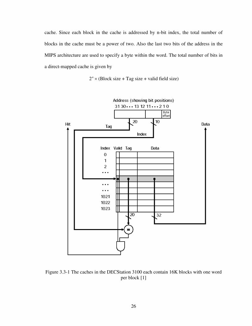
26
cache. Since each block in the cache is addressed by n-bit index, the total number of
blocks in the cache must be a power of two. Also the last two bits of the address in the
MIPS architecture are used to specify a byte within the word. The total number of bits in
a direct-mapped cache is given by
×n2 (Block size + Tag size + valid field size)
Figure 3.3-1 The caches in the DECStation 3100 each contain 16K blocks with one word
per block [1]

27
3.1.2 Fully-associative cache
In a fully associative cache, any block from memory can be placed in any location in the
cache. To find a given block in a fully associative cache, all the entries in the cache must
be searched and for making the search practical, comparison is done in parallel with each
associated cache entry. This results in the use of more comparators thereby increasing the
hardware cost by a significant amount effectively making fully associative placement
practical only for caches with small blocks. The following table shows the advantages
and disadvantages of using various types of cache and we can see that direct mapped is
best cost-wise but fully-associative is best performance wise.
Table 3.1 Mapping function comparison table
Cache Type Hit Ratio Hardware
Complexity
Search speed
Direct-mapped Good Simple Best
Fully associative Best Complex Moderate
N-way set
associative, N>1
Very good, better as
N increases
Moderate Good, worse as N
increases
3.1.3 N-way associative cache
This scheme falls in between direct mapped cache where N = 1 and fully associative
cache where N = total number of blocks in the cache. In this scheme, there are a restricted
number of locations in the cache where a block of memory can be placed. An n-way set
associative cache consists of a number of sets, each of which consists of n blocks. Each
28
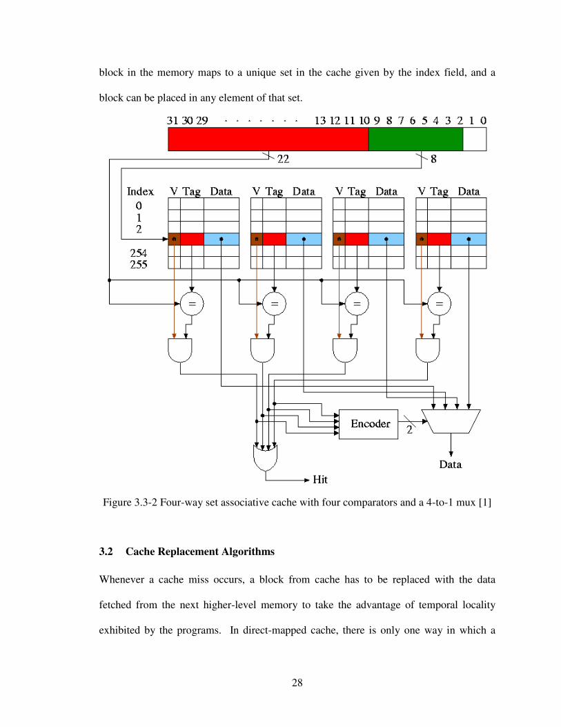
block in the memory maps to a unique set in the cache given by the index field, and a
block can be placed in any element of that set.
Figure 3.3-2 Four-way set associative cache with four comparators and a 4-to-1 mux [1]
3.2 Cache Replacement Algorithms
Whenever a cache miss occurs, a block from cache has to be replaced with the data
fetched from the next higher-level memory to take the advantage of temporal locality
exhibited by the programs. In direct-mapped cache, there is only one way in which a
29
block can be placed in the memory because every block in memory is mapped to a single
location in the cache. Whereas in a fully associative or set associative, there is more than
one locations in cache to where every location from memory can be mapped. A
replacement policy has to be chosen for cache for selecting the block to be evicted. There
are three primary replacement policies in use – FIFO, LRU and Random. First In First
Out (FIFO) replacement policy replaces the oldest block in the set. An (LRU) policy
replaces the least recently used block in the set and a random policy chooses a block to be
evicted randomly.
LRU is based on the strategy that if a block has been used more recently by the processor,
then it is more likely to be used again. This policy needs a significant amount of
hardware for its implementation that is quite complex and so is not very attractive. Also
the policy itself is based on an assumption that the block that is used least recently has
much less chances of being used as compared to any other blocks that are used more
recently. FIFO policy is a further approximation of LRU since this assumes that if a block
has been loaded in cache a long time ago, it might not have been referenced for a while.
This is not so complex to implement because the oldest can be computed by simply time
stamping the blocks when they are first allocated in the cache. Random replacement
policy is not so preferred a policy since this might evict the wrong block periodically as
compared to systematic eviction of wrong blocks that might occur in LRU or FIFO
policies. And since computers in nature are not random, it is not very simple to
implement a truly random policy.
30
3.3 Cache-Memory Interaction
When cache reports a hit on the memory reference, the machine continues using the data
as if nothing had happened. But when the control unit detects a read miss, it has to
process the miss by fetching the data from the memory or a lower-level cache. The basic
approach to handle the miss is to stall the CPU, freezing the contents of all the registers.
A separate controller to which the control is transferred on a miss fetches the data into the
cache/CPU from lower-level cache or memory. Once the data is available, execution is
resumed at the cycle that caused the cache miss.
Read misses are easy to handle because on a read miss, data from the next level of
memory hierarchy is fetched and replaced into cache while the block that is evicted is
chosen based on the replacement policy used.
However, modifying a block in cache during a write operation cannot begin until the tag
is checked to see if the address is a hit. Only the portion of the block specified of size
between 1 and 8 bytes by the processor has to be changed leaving the rest of the block
unchanged. In contrast, reads can access more bytes than necessary without a problem.
On a cache miss, data cannot simply be written in the cache since the data constitutes
only a part of the block and therefore the entire block has to be fetched before a write to
cache for the whole block to be valid. There are two ways of handling this. One is a
‘write-allocate scheme’ in which the block is fetched from main memory into cache first
and then the data is written into the cache. In a non-allocating cache scheme, the first-
level of cache is simply bypassed and the data is written only in main memory or the next
level of cache.
31
On a write hit for a write-back scheme, only cache is updated with the new data, and after
the write into the cache, memory would have a different value from that in the cache. So
there should be a way to recognize the block as ‘dirty’ with a status bit and the memory
has to be updated with the valid content before the block is evicted from the cache.
Advantages of write-back cache are that the writes occur at the speed of the cache
memory and that the multiple writes within a block require only one write to main
memory resulting in less memory bandwidth usage. This scheme is harder to implement
and the reads that result in replacement of the dirty block causes memory writes.
The other scheme in which both copies in the cache and memory are updated
simultaneously on a write miss is called ‘write-through cache’. The advantages of the
write-through scheme over the ‘write allocate scheme’ are that the read miss never results
in writes to main memory, it is easy to implement and the data in the main memory is
always consistent. On the down side, the writes are slower because memory-write which
is a lot slower than cache-write has to be performed for every write on miss which results
in usage of more memory bandwidth.
Combining the schemes for write hit with write miss result in four possible combinations.
In write-through with write-allocate, bringing the block to cache on a miss is not useful
because the next hit to this block will generate a write to main memory (according to
Write Through policy). In write-through with no write allocate policy, subsequent writes
to the block will update main memory and so, time is saved not bringing the block in the
cache on a miss because it appears useless anyway. In write-back with write-allocate,
subsequent writes to the same block, if the block originally caused a miss, will hit in the
cache next time, setting the dirty bit for the block. That will eliminate extra memory
32
accesses and result in very efficient execution compared with the write-through with
write-allocate combination. Write-back with no write-allocate of subsequent writes to the
same block, if the block originally caused a miss, will generate misses all the way and
result in very inefficient execution.
3.4 Cache Performance Metrics
Average memory access time in a computer system is a measure to evaluate performance
of cache in a memory hierarchy. It can be calculated using the formula,
Average memory access time = hit time + miss rate × miss penalty …………(3.1)
The time obtained using the above formula can be converted into CPU cycles for a given
CPU frequency. Memory system performance in a CPU relative to other operations in the
CPU like program execution is obtained by using the memory access time in CPU cycles
rather than in nanoseconds.
Access time for instruction cache and data cache might have to be calculated separately
since they both might have different penalties. Also read access time and write access
time within data cache can be separated as they might have different miss rates and also
different penalties.
When a memory system performance is evaluated relative to a CPU with low clock
cycles per instruction (CPI), the system might suffer more since the penalty will be a
significant amount of the total time. This might not be the case for a CPU with high CPI.
From the equation 3.1, there are three ways of reducing average memory access time and
they are reducing hit time, reducing miss rate or reducing miss penalty.
33
This as well as other important metrics like the number of evictions for a given program,
eviction rate, effect of a victim cache on the eviction rate or some things in which both
the architecture designer as well as programmer would be interested in, should be easily
measurable with a model developed for the cache. The proposed model [detailed in
chapter 4] being modular helps in easy addition and measurement of such performance
metrics an end user might be interested in.
3.4.1 Cache Miss Types
Every cache miss falls into one of the three categories explained. ‘Compulsory miss’ is a
cache miss that occurs for the first-ever reference to a given block. Since a first access to
a block cannot be in the cache, there must be a compulsory miss. A miss that occurs on
the blocks that would have been discarded when cache is too small to hold all of the
blocks needed during execution of a program is called a ‘capacity miss’. It is the
difference between the compulsory miss rate and the miss rate of a finite size fully
associative cache. The third type of cache misses called ‘conflict misses’ occur due to
placement restrictions that cause useful blocks to be displaced. This is like a capacity
miss within a set. It is given by the difference between the miss rate of a non-fully
associative cache and a fully associative cache. Reducing any of the above said cache
misses could reduce the miss rate of a memory system.
There are several ways of reducing miss rate as explained below:
1. Larger cache blocks
34
Larger cache blocks decrease compulsory misses, but they may increase the miss
penalty by requiring more data to be fetched per miss. Conflict misses also
increase, since fewer blocks can be stored in a given cache. High latency and high
bandwidth memory systems tend to use large block sizes since cache gets more
bytes per miss for a small increase in miss penalty.
2. Higher cache associativity
Higher associativity decreases conflict misses at the expense of extra hardware
and increased hit times. Increased hit-times impose upper limits on the degree of
associativity as the hit rate is offset by the slower clock cycle time. Generally
associativity of 8 is the largest one used for most of the memory systems.
3. Victim caches
Victim cache is used to store a few of the blocks that are eliminated from a
processor cache during replacement. The processor checks victim cache on L1
cache miss before it goes to main memory. Since victim cache will have far less
memory access time than the main memory, the miss penalty is reduced.
4. Hardware prefetch
This is a technique of fetching the data before it is requested thereby reducing
compulsory cache misses. Prefetched blocks are held in a separate buffer until
they are used in order to prevent eviction of useful blocks. Prefetching uses main
memory bandwidth and thus might affect the performance if prefetched data is not
used or if the prefetch process interferes with the main memory access on cache
misses.

35
3.5 Cache Addressing
As explained in section 2.1, virtual addressing is implemented to make more efficient use
of real physical memory by making it appear like a contiguous working memory to the
programs. To summarize, each program running on the machine sees its own simplified
address space and accesses it without regard for what other programs are doing in their
address spaces. The memory management unit (MMU) is the portion of the processor that
does the translation from a program’s virtual address to a real physical memory address.
Most modern level-1 caches are virtually indexed. Since a virtually indexed cache does
not have to perform virtual to real address translation for accessing cache, speed is
improved. This also allows the MMU’s TLB lookup to proceed in parallel with fetching
the data from the cache. But due to virtual aliases (different virtual addresses referring to
a single physical addresses by different programs), there might be multiple locations in
the cache which store the value of a single physical address. This is handled by
guaranteeing only one virtual aliased address is present in the cache at any give time. For
an n-way set associative cache, whenever a cache write occurs, the processor searches for
virtually aliased addresses among those n-ways and evicts them first and since this is
done only when there is a cache miss, no extra work is required since the checks would
have already performed while checking for a cache hit.
Virtual tagging is not much used since the TLB lookup for a tag can be finished by the
time cache is indexed and tag compare has to be performed. But the advantage of virtual
tagging is that the tag match can be done well before address translation is done.
36
3.6 Cache hierarchy
Since pipelined CPUs access memory from multiple points in the pipeline during
instruction fetch, data fetch and address translation, four separate caches: instruction
cache, data cache, ITLB and DTLB are included so that one cache doesn’t have to serve
two points in the pipeline.
Victim cache is used to store blocks that are eliminated from a processor cache during
replacement. It lies between the main cache and the next level of memory from where the
data is fetched into main cache. Victim cache reduces penalty on cache miss, if a block
that was very recently evicted is referenced again.
Trace cache is a technique that helps in increasing fetch bandwidth and in decreasing
power consumption by storing traces of instruction that have already been fetched and
decoded. Decoded instructions are added to trace caches in groups representing either
dynamic instruction traces or individual blocks. Blocks consist of a group of non-branch
instruction ending in a branch. Dynamic trace consists of only instructions that have been
used. All the unused instructions like instructions following taken branches are
eliminated. Trace lines are stored in trace cache based on multiple paths that are possible
with the first instruction in the trace based on the program counter. This branch
prediction is encountered for and thus can supply the trace line upon the outcome of
branch condition.
Multi-level caches constitute of small fast caches backed up by large slower caches to
eliminate the tradeoff between cache latency and hit rate that arises in larger caches.
Three-level on chip caches are being used as the latency difference between main
memory and the fastest cache is becoming significantly larger.
37
Multi-level caches can be either inclusive or exclusive. In an inclusive cache, all the data
present in the L1 cache should also be present in L2 cache. In case of exclusive caches,
L1 cache and L2 cache are exclusive in terms of the data content. Exclusive cache can
store more data and is advantageous especially for larger caches. Since strictly inclusive
caches have a copy in L2 cache, on eviction of data in L1 cache (occurs especially in
multiprocessor systems), processor can access L2 cache with much more speed than
accessing next higher level of memory.
3.7 Cache coherency algorithms for multi-ported and multi-processor
environments
In multi-processor systems, since all the processors see the same main memory, caches
cannot be operated independently as the dirty caches updated by one processor has to be
seen by the other. The uniform view of memory, as shown in figure 3.1, is called cache
coherency. Providing access for every processor with every cache is very expensive.
Cache coherency can be achieved by making a processor detect a write request by any
processor and then by making the referenced data in its own cache, if present, invalid
(this process is called snooping). Another way is to find the dirty block if present in one
of the other caches and send the data from cache directly to the processor that requested
read or write. Finding out if the cache line in another processor’s cache is dirty, by
broadcasting information about changed cache lines after each write access, would be
impractical.

38
Figure 3-3 Cache Coherent System
There are several cache coherency protocols that could be used for a cache coherent
system. Each of the coherence protocols differs from others in terms of scalability (how
the size of bus and bandwidth have to be scaled with the size of the system) and
performance. Implementation of each of these protocols might be based on different
invalid and update transitions. Choice of transition may affect the effective cache
bandwidth available for work.
MOESI (Modified Owned Exclusive Shared Invalid) protocol has five possible states that
each and every cache line should fall in. All of these states are explained below [17]:
1. Modified – A cache line is said to be in modified state if the cache line holds the
recent most data updated by its corresponding processor and the cache line is dirty
(memory still not updated). It also means no other caches have a copy of it.
2. Owned – A cache line is said to be in an owned state when it holds the most
recent copy of data and the main memory is updated with the recent data too.
Other caches can have the updated data too, but only one cache line among all
valid cache lines can be in the owned state. All others will be in the shared state.
39
3. Exclusive – a cache line is said to be in the exclusive state if it holds the most
recent, correct data with correct data in main memory and with no other copies of
it in other caches.
4. Shared – the shared state is similar to the owned state except that none of the
caches here are in owned states, but every cache line with the copy is in the
shared state with recent values updated for all copies of it including in memory.
5. Invalid – a cache line is said to be in the invalid state if the cache doesn’t hold a
valid copy of data. Valid data might be either in main memory or in other
processor’s cache.
As long as the system components select options dynamically, memory system state
remains consistent. Since implementing a 5-state protocol on on-chip caches can be quite
expensive, another protocol MESI with 4 states is directly derived. The “Owned” state in
MESI is eliminated by making modified and shared states illegal to be present at the
same time. Various cache coherent models are listed here most of which are derived from
MOESI: MSI protocol, MESI protocol, Berkeley protocol, Dragon protocol, MOSI
protocol, Illinois protocol, Firefly protocol and write-once protocol.
3.8 Latency and bandwidth
Block based trace cache and similar approaches have been used to improve the fetch
bandwidth and the latency. These differ from the basic trace cache in the principle that
one basic block is stored only once even though it might be part of several traces. This
avoids the duplication problem in trace cache thereby allowing the block cache to have
smaller size and still provide the same efficiency in terms of miss rates.

40
3.9 Cache Modeling
Modeling is an act of representing a system or a subsystem formally []. A model is used
to understand the performance of a system based on various parameters and the tradeoffs
involved in it. Programs are executed on a software model to validate a proposed
hardware design’s performance. Modeling facilitates simulating the architectural model
that helps the designers to evaluate the performance and correctness of the system
thereby providing them with more design space exploration. Figure 3.4 shows a block
diagram of how a systematic exploration of the architecture is to be performed to tune it
up to an application domain overcoming the performance loss due to the distinction
between application and architecture. An application engineer would be able to code
profile his application with different architectures and choose the best one out of the
available architectures by comparing performance metrics like throughput, hit rate,
average memory access time, IPC, etc..
Figure 3-4 Cache Model: Mapping Architecture and Application [8]
41
Since the electronics market and its applications are growing far more rapidly than ever
offering products at lower costs and higher performance, there is pressure imposed on the
design community, which is making them seek techniques for design automation and
reuse that would accelerate the progress. Cache modeling has become one of the
significant techniques owing to the importance of the memory hierarchy on performance
of the programmable systems.
42
CHAPTER 4
IMPLEMENTATION OF THE CACHE MODEL
4.0 Introduction
A modular cache memory model that is cycle accurate (and thereby fast)
has been developed for simulating various levels and types of cache to quickly evaluate
the trade-offs between cache size, cache policy and cache levels versus system
performance in terms of IPC and cost. The developed cache model was interfaced with a
MIPS IV instruction set simulator called ‘Sysabakus’ [20] that was developed at OSU.
The processor consists of both a linear in-order pipeline model and also an N-
wide out-of-order processor with ALU, multiply, branch and load/store units. It also
consists of an N-wide fetch front-end which would fetch N-instructions every single
cycle and would try to decode, issue and retire a similar number of instructions every
cycle. The fetch module was initially using a perfect memory model where any data
requested was available instantaneously without any delay. This fetch module was
modified to instruction cache, which would include all cycle latencies that are needed for
performance evaluation. The fetch module would also control the fetch PC based on a hit
or miss from the cache. It would also insert NOP’s for the decode/issue unit for all
missed instructions until a hit for a given address is achieved. The cache controller also
included all counters that would be needed for performance evaluation.
43
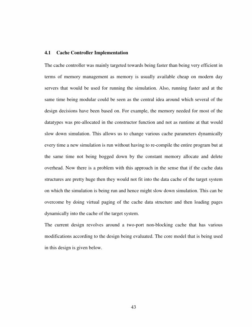
4.1 Cache Controller Implementation
The cache controller was mainly targeted towards being faster than being very efficient in
terms of memory management as memory is usually available cheap on modern day
servers that would be used for running the simulation. Also, running faster and at the
same time being modular could be seen as the central idea around which several of the
design decisions have been based on. For example, the memory needed for most of the
datatypes was pre-allocated in the constructor function and not as runtime at that would
slow down simulation. This allows us to change various cache parameters dynamically
every time a new simulation is run without having to re-compile the entire program but at
the same time not being bogged down by the constant memory allocate and delete
overhead. Now there is a problem with this approach in the sense that if the cache data
structures are pretty huge then they would not fit into the data cache of the target system
on which the simulation is being run and hence might slow down simulation. This can be
overcome by doing virtual paging of the cache data structure and then loading pages
dynamically into the cache of the target system.
The current design revolves around a two-port non-blocking cache that has various
modifications according to the design being evaluated. The core model that is being used
in this design is given below.
44
EVENT/COMMAND QUEUE
CACHE DATA
CPU PORT
CPU/L1
MEMORY PORT
MEMORY/L2
REPLACEMENT
CONTROLLER
Command
& Data
Command
& Data
Data
Data
CACHEREAD & CACHEWRITE
MEMREAD & MEMWRITE
COMMAND ADDRESS SIZEDATA
POINTERLATENCY
VALID DIRTY TAG DATA CNTR
Figure 4-1 Block Diagram of the Cache Controller
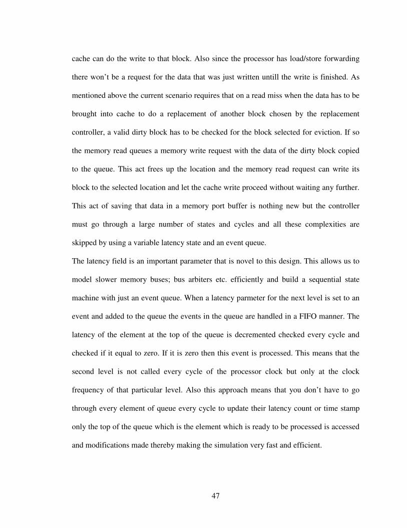
As you can see there are five main blocks for the cache controller in the above diagram
and each one of these is implemented in separate modules/functions so that it is very easy
to modify one part and evaluate the performance gain without affecting the other parts.
This modular design would also help in extending this cache model to fit future
applications like multiple ports and multi-processor interfaces. Adding new performance
45
metrics for something like this modular design would be very easy since this can be done
without affecting the other parts and just adding one separate module that would give
new performance metrics.
The main part that gives this cache its flexibility is the event queue controller. It is a
linked list which both the CPU port and the memory port (the memory port could actually
be lower level cache and the CPU port could be interface to a higher level cache) to
queue requests in case of misses or evictions.
There is a latency field in the queue which allows for states in the queue to have variable
delays before they are eventually fetched and requests completed. The latency field also
allows for simulating the slower cycle memory bus by not even issuing a memory read
request until the latency parameter gets to zero. So each level of cache memory running
at different clock rates can easily be simulated by just setting the latency parameter to be
variable for each level. Also, since the states can now have variable latency it allows the
controller to have a lot fewer states than would be present in a normal cache controller. In
fact, the current implementation of the cache controller consists of only 4 states called
CACHEREAD, CACHEWRITE, MEMREAD and MEMWRITE. As you can see from
the list of states, there are no states separately for evictions for when waiting for evictions
to happen. This is all hidden by the variable latency states and hence the controller itself
simulates a lot faster with only the necessary details that are required for a cycle accurate
simulation.
An example of some common cases that can be handled with just these four states is
given below. Consider a write back cache in the case of write miss. Also let the location
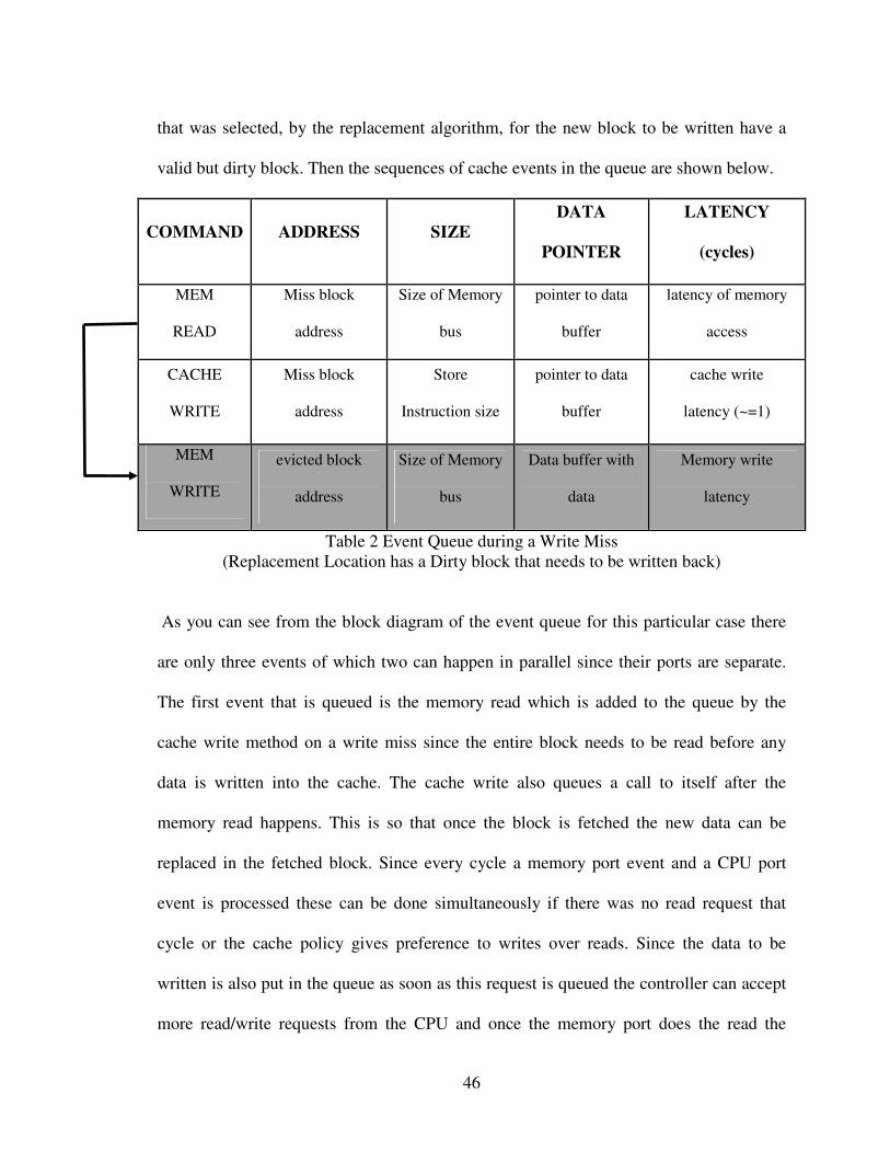
46
that was selected, by the replacement algorithm, for the new block to be written have a
valid but dirty block. Then the sequences of cache events in the queue are shown below.
COMMAND ADDRESS SIZE
DATA
POINTER
LATENCY
(cycles)
MEM
READ
Miss block
address
Size of Memory
bus
pointer to data
buffer
latency of memory
access
CACHE
WRITE
Miss block
address
Store
Instruction size
pointer to data
buffer
cache write
latency (~=1)
MEM
WRITE
evicted block
address
Size of Memory
bus
Data buffer with
data
Memory write
latency
Table 2 Event Queue during a Write Miss
(Replacement Location has a Dirty block that needs to be written back)
As you can see from the block diagram of the event queue for this particular case there
are only three events of which two can happen in parallel since their ports are separate.
The first event that is queued is the memory read which is added to the queue by the
cache write method on a write miss since the entire block needs to be read before any
data is written into the cache. The cache write also queues a call to itself after the
memory read happens. This is so that once the block is fetched the new data can be
replaced in the fetched block. Since every cycle a memory port event and a CPU port
event is processed these can be done simultaneously if there was no read request that
cycle or the cache policy gives preference to writes over reads. Since the data to be
written is also put in the queue as soon as this request is queued the controller can accept
more read/write requests from the CPU and once the memory port does the read the
47
cache can do the write to that block. Also since the processor has load/store forwarding
there won’t be a request for the data that was just written untill the write is finished. As
mentioned above the current scenario requires that on a read miss when the data has to be
brought into cache to do a replacement of another block chosen by the replacement
controller, a valid dirty block has to be checked for the block selected for eviction. If so
the memory read queues a memory write request with the data of the dirty block copied
to the queue. This act frees up the location and the memory read request can write its
block to the selected location and let the cache write proceed without waiting any further.
This act of saving that data in a memory port buffer is nothing new but the controller
must go through a large number of states and cycles and all these complexities are
skipped by using a variable latency state and an event queue.
The latency field is an important parameter that is novel to this design. This allows us to
model slower memory buses; bus arbiters etc. efficiently and build a sequential state
machine with just an event queue. When a latency parmeter for the next level is set to an
event and added to the queue the events in the queue are handled in a FIFO manner. The
latency of the element at the top of the queue is decremented checked every cycle and
checked if it equal to zero. If it is zero then this event is processed. This means that the
second level is not called every cycle of the processor clock but only at the clock
frequency of that particular level. Also this approach means that you don’t have to go
through every element of queue every cycle to update their latency count or time stamp
only the top of the queue which is the element which is ready to be processed is accessed
and modifications made thereby making the simulation very fast and efficient.
48
4.2 Replacement Controller
The algorithm that selects the block to be replaced is the one that is researched
and optimized the most in a cache since this directly decides the cache performance in
terms of capacity misses and compulsory misses. Hence this block has been implemented
as a separate module called the replacement controller. The current version of the
replacement controller models FIFO, pseudo LRU and random. A proper random or LRU
controller cannot be implemented easily in hardware and hence to model this in software
a pseudo LRU [18] and random model that could be easily implemented in hardware has
been chosen to look at the performance of these algorithms.
The primary addressable element that is stored in the cache is one word (4bytes for this
MIPS architecture). This was chosen for two reasons:
1. The word data type is the one that is most frequently used by the processor,
always words are accesses by the instruction cache and mostly words are accessed
by the Data cache, so using a primary datatype of word speeds up these accesses.
Although words are the primary data structure, primitives for reading/writing a
byte and half words are provided which work by reading the word and then
separating the byte/half-word for a read, and read a word modify the byte/half-
word and write back the word for a write access. As you can see these primitives
are pretty slow since they require 2 or 3 operations per access but since these are
used very rarely the use of word addressing is justified.
2. The smallest data that can be read out of modern 32-bit or 64-bit processors is 4
bytes thereby making the access for words a lot faster during simulation.
49
The event queue linked list that is currently used is based on the STL (Standard Template
Library) [19] and hence can be easily modified to a thread safe list class without any
change to the list access functions itself. This might be necessary in the future when there
is several memory and CPU ports and we want to run them as individual threads with all
threads accessing and updating the event queue simultaneously. The use of STL classes
provides this flexible switching of classes without a change to the member functions.
4.3 Constraints in Current Design
1. Although the Memory fetch port can be parameterized to any number of bytes in
the constructor, the class wont accept any cache block size that is not an integer
multiple of the memory bus size. This is done to ease the event queue design
where if the cache block is an integer multiple of the memory bus size then the
integer number of memory read/write requests can be queued with their address
offset and then cache can then proceed with what it was doing without waiting for
the memory port to get free.
2. The latency field of the event queue only allows for integer values and hence all
clocks for various levels of memory should be integer multiples of other levels.
This cannot be easily modified either since the latency is decremented or issued
only once every clock cycle of the higher level.
3. Using a multi-threaded port means use of a multi-threaded queue which for easier
change would mostly be an STL thread-safe queue like the Boost Library
50
[www.boost.org]. This is usually terribly slower than non thread safe versions and
might slow the simulation quite a bit.
4.4 Implementation Issues on a sequential Processor
There are several restrictions in simulating a lot of hardware, that are essentially by
design parallel in nature, in software on a sequential processor which leads to some
design trade-offs and modifications. Similarly what can easily be done using complex
algorithms in software might take a lot of silicon area to implement in hardware and are
hence not cost effective. While modeling the cache structure, such problem were faced as
well which are detailed below along with steps taken to work around the problem.
Implementing a true LRU policy in hardware is very expensive as it requires keeping
track of exactly when and which of the ways in a set were accessed. Several solutions
have been proposed to this problem that are easy to implement in hardware and are cost
effective [18]. Hence to show/analyze/determine the actual performance impact of using
these compromised algorithms a pseudo LRU replacement algorithm that just uses one
counter per set was used. This counter is incremented during every hit to point to the
way one above the hit. Doing so basically splits the ways into two sets where above the
location pointed to by the counter, there are locations that have not been accessed in the
current period (one period is when the counter overflows and resets itself to zero) and
below that counter are ways that have might have been recently accessed although not
necessarily. Also the random replacement policy was implemented by bit shifting the
counter and exoring some bits in the counter to achieve a random output.
51
Similarly to make copying of data from memory to cache easier the ‘memcpy’ function
was used which copies several bytes of data at once although this might not be practically
feasible on a hardware cache controller.
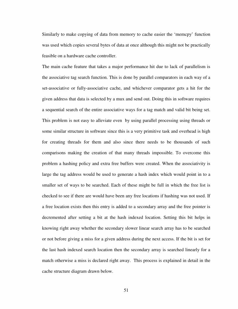
The main cache feature that takes a major performance hit due to lack of parallelism is
the associative tag search function. This is done by parallel comparators in each way of a
set-associative or fully-associative cache, and whichever comparator gets a hit for the
given address that data is selected by a mux and send out. Doing this in software requires
a sequential search of the entire associative ways for a tag match and valid bit being set.
This problem is not easy to alleviate even by using parallel processing using threads or
some similar structure in software since this is a very primitive task and overhead is high
for creating threads for them and also since there needs to be thousands of such
comparisons making the creation of that many threads impossible. To overcome this
problem a hashing policy and extra free buffers were created. When the associativity is
large the tag address would be used to generate a hash index which would point in to a
smaller set of ways to be searched. Each of these might be full in which the free list is
checked to see if there are would have been any free locations if hashing was not used. If
a free location exists then this entry is added to a secondary array and the free pointer is
decremented after setting a bit at the hash indexed location. Setting this bit helps in
knowing right away whether the secondary slower linear search array has to be searched
or not before giving a miss for a given address during the next access. If the bit is set for
the last hash indexed search location then the secondary array is searched linearly for a
match otherwise a miss is declared right away. This process is explained in detail in the
cache structure diagram drawn below.
52
Valid
.
.
.
.
.
.
.
.
.
Dirty
.
.
.
.
.
.
.
.
.
Tag
.
.
.
.
.
.
.
.
.
Data
.
.
.
.
.
.
.
.
.
Counter
.
.
.
.
.
.
.
.
.
Linear
.
.
.
.
.
.
.
.
.
128
3
4
.
.
.
.
.
.
.
2
1
TAG31 30 29………………………….…..11 10 9 8…………..……….4 3 21
7Block
and
Word
Address
FREE COUNT
0
1
Figure 4-2 Hash based fast indexing for fully-associative cache
On a cache miss, if all valid bits are 1 and linear bit is 1 search the linear cache
53
Valid
.
.
.
.
.
.
.
.
.
Dirty
.
.
.
.
.
.
.
.
.
Tag
.
.
.
.
.
.
.
.
.
Data
.
.
.
.
.
.
.
.
.1023
1024
.
.
.
.
.
.
.
1
2
3
4
5
31 30 29………………………….…..11 10 9 8…………..………….4 3 21
32
Tag
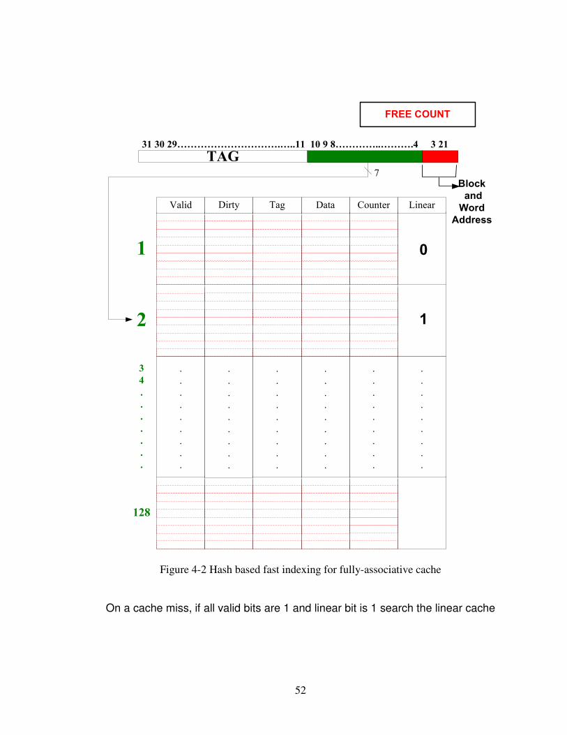
Figure 4-3 Hash indexing for a fully associative cache
54
CHAPTER 5
SUMMARY AND CONCLUDING REMARKS
5.0 Results
Several different cache configurations and architectures were evaluated in simulation and
their performance metrics for various SPEC benchmarks are listed below. The processor
simulator used to test the cache was Abakus [20] developed at Oklahoma State
University, which simulates MIPS IV instruction sets. There are two versions of the
abakus processor available. One, a linear pipeline which fetches and executes a single
instruction per cycle in instruction order and uses a branch evaluation in the execute
stage. The second is a highly configurable superscalar simulator with out-of-order
execution capability. The configuration used for the superscalar processor for all
simulations was a 4-wide instruction fetch with a perfect branch prediction and 4 ALU,
Multiply and Load/Store units. All tests programs were taken from the SPEC-95
benchmarks or SPEC-2006 benchmarks compiled for the MIPS-IV instruction set.
55
5.0.1 Simulation of a single level instruction cache with linear pipeline
The first simulation that was carried out was a simple linear pipeline with a single level
of 1K instruction cache with 4-way set associativity. This model was used for simple
measurements like read hit and misses as well as for evaluating cache replacement
algorithms such as pseudo-LRU using counters [18]. The performance of the cache
simulation code itself was measured using a comparison of the seconds needed to
simulate a given benchmark program. The results for a linear pipeline showed that the
cache was causing the simulator to slow down only by about 2 times as compared to 10-
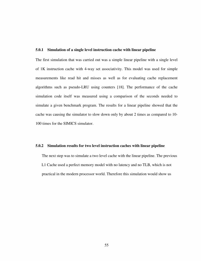
100 times for the SIMICS simulator.
5.0.2 Simulation results for two level instruction caches with linear pipeline
The next step was to simulate a two level cache with the linear pipeline. The previous
L1 Cache used a perfect memory model with no latency and no TLB, which is not
practical in the modern processor world. Therefore this simulation would show us
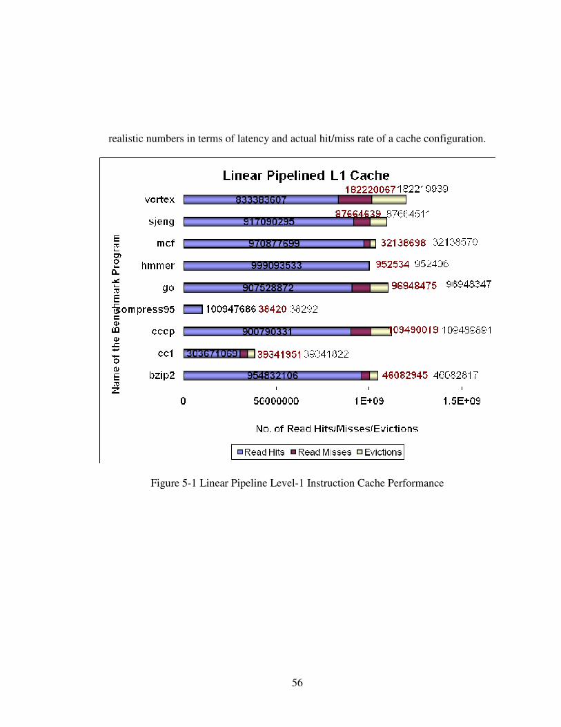
56
realistic numbers in terms of latency and actual hit/miss rate of a cache configuration.
Figure 5-1 Linear Pipeline Level-1 Instruction Cache Performance
57
Figure 5-2 Linear Pipeline Level-2 Instruction Cache Performance
5.0.3 Simulation of four-issue cache for four-wide superscalar
The next simulation was to make the Cache-CPU bus width larger to accommodate
for a larger fetch width of the superscalar processor. The L1 cache was set to provide four
instructions every cycle.

58
Figure 5-3 Performance of a 1K 4-way cache for a four-issue out-of-order processor
5.0.4 Miss Rate Curves for various sizes of instruction cache
The size of the cache and the associativity of the cache were varied and the miss rates for
various benchmark programs were plotted to look for a general trend on the behaviour
and performance of a given size and associativity cache. Data from the sim-cache
simulator which is part of the simplescalar toolset [www.simplescalar.com] were also
plotted for the direct mapped cache to check if the same general trend was observed. The
plots for two SPEC95 benchmark programs compress95 and cc1 are shown below.
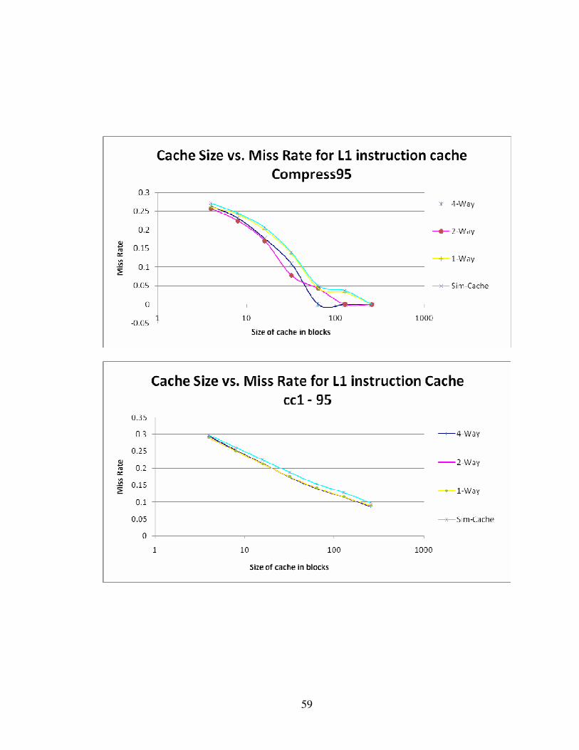
59
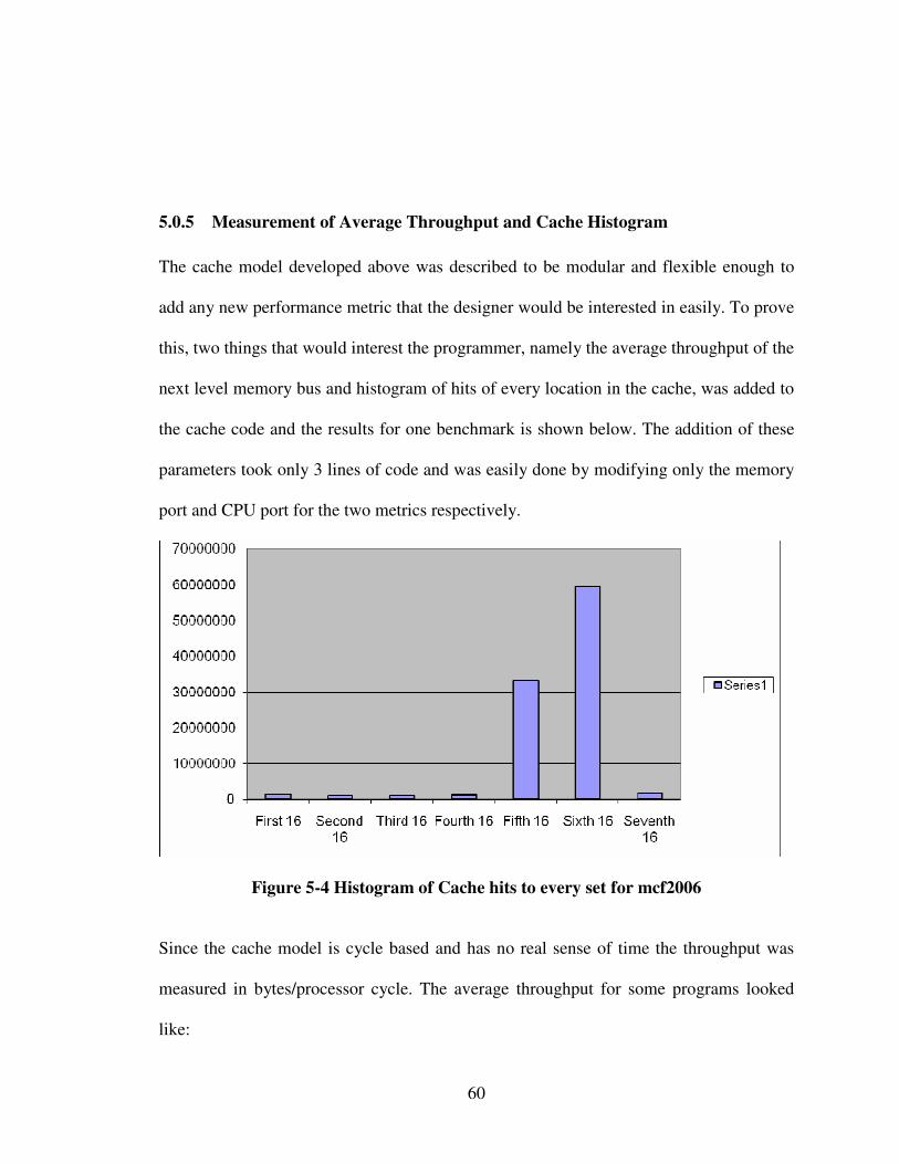
60
5.0.5 Measurement of Average Throughput and Cache Histogram
The cache model developed above was described to be modular and flexible enough to
add any new performance metric that the designer would be interested in easily. To prove
this, two things that would interest the programmer, namely the average throughput of the
next level memory bus and histogram of hits of every location in the cache, was added to
the cache code and the results for one benchmark is shown below. The addition of these
parameters took only 3 lines of code and was easily done by modifying only the memory
port and CPU port for the two metrics respectively.
Figure 5-4 Histogram of Cache hits to every set for mcf2006
Since the cache model is cycle based and has no real sense of time the throughput was
measured in bytes/processor cycle. The average throughput for some programs looked
like:
61
� Compress95 – 1.41429 bytes/cycle
� cc1 – 1.88725 bytes/cycle
� go – 0.630861 bytes/cycle
5.0.6 Measurement of Average Latency
The measurement of average latency of a given level of the cache is very important since
it is measuring overall how effective is the cache in keeping the processor busy
irrespective of the slow lower memory levels. In the current model, since it is modular,
the measurement of average latency could be easily done without much change to the
current cache configuration. The main change needs to come in the CPU port code to
increment the latency counter for every cache read event in the Event queue. Once a
cache read event comes to the top, ready to be satisfied, the CPU port uses the latency
count for this particular event to update the average latency up to that point. These
changes would take only a few lines of code and provide valuable information using the
already existing architecture.
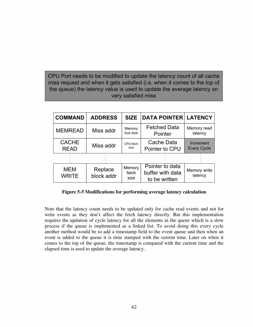
62
COMMAND ADDRESS SIZE DATA POINTER LATENCY
MEMREAD Miss addrMemory
bus size
Fetched Data
PointerMemory read
latency
CACHE
READMiss addr
CPU fetch
size
Cache Data
Pointer to CPUIncrement
Every Cycle
MEM
WRITE
Replace
block addr
Memory
fetch
size
Pointer to data
buffer with data
to be written
Memory write
latency``
CPU Port needs to be modified to update the latency count of all cache
miss request and when it gets satisfied (i.e. when it comes to the top of
the queue) the latency value is used to update the average latency on
very satisfied miss
Figure 5-5 Modifications for performing average latency calculation
Note that the latency count needs to be updated only for cache read events and not for
write events as they don’t affect the fetch latency directly. But this implementation
requires the updation of cycle latency for all the elements in the queue which is a slow
process if the queue is implemented as a linked list. To avoid doing this every cycle
another method would be to add a timestamp field to the event queue and then when an
event is added to the queue it is time stamped with the current time. Later on when it
comes to the top of the queue, the timestamp is compared with the current time and the
elapsed time is used to update the average latency.
63
5.1 Conclusion
A cycle accurate cache model has been developed and tested as an instruction
cache with both a linear pipeline as well as an out-of-order multi-instruction issue
superscalar processor. Since the model did not actually model all the internal states of a
cache controller but effectively mimicked them using a variable latency event queue this
model was very fast and efficient when compared to other similar cache models. The ease
with which one can add several desired performance metrics was shown by adding
metrics such as average throughput and a histogram of hits for every set. Several integer
SPEC2006 and SPEC95 benchmarks were run to check whether the cache model had any
underlying problems and this was verified by two methodologies. There is an inbuilt
checker internal to the cache that when enabled in debug mode checks for the validity of
all data, with the main memory, as they are fetched by the processor. Also the final
output produced by the simulated SPEC benchmark was compared with the reference
output that comes along with the benchmark to verify that the program did follow the
exact same direction and gave the same output. A third verification for the performance
metrics such as number of hits or miss ratio was done by setting the sim-cache
[www.simplescalar.com] with similar parameters and running the same benchmarks.
Although this would not give the exact same numbers since the processor models are
different (for example the linear-pipeline would fetch and then flush two instructions in
case of a mis-predicted branch but sim-cache uses a perfect predictor in the fetch stage
and hence never fetches any waste instructions) they matched to the first order properly.
All these verifications showed that the developed processor model is correct for the
instruction cache.
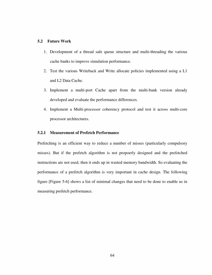
64
5.2 Future Work
1. Development of a thread safe queue structure and multi-threading the various
cache banks to improve simulation performance.
2. Test the various Writeback and Write allocate policies implemented using a L1
and L2 Data Cache.
3. Implement a multi-port Cache apart from the multi-bank version already
developed and evaluate the performance differences.
4. Implement a Multi-processor coherency protocol and test it across multi-core
processor architectures.
5.2.1 Measurement of Prefetch Performance
Prefetching is an efficient way to reduce a number of misses (particularly compulsory
misses). But if the prefetch algorithm is not propoerly designed and the prefetched
instructions are not used, then it ends up in wasted memory bandwidth. So evaluating the
performance of a prefetch algorithm is very important in cache design. The following
figure [Figure 5-6] shows a list of minimal changes that need to be done to enable us in
measuring prefetch performance.
65
Figure 5-6 Modifications for a prefetch performance measurement
66
REFERENCES
[1] David A. Patterson, John L. Hennessy, “Computer Organization and Design: The
Hardware/Software Interface,” 2nd
edition, 1996, Morgan Kauffman Publishers.
[2] http://simplescalar.com/
[3] www.faculty.iu-bremen.de/.../cache%20memory.htm
[4] http://www.faculty.iu-bremen.de/birk/lectures/PC101-
2003/07cache/cache%20memory.htm
[5] R. Sam, “ZOOM: A Performance-Energy Cache Simulator,” S. B. Electrical and
Computer Science, Massachusetts Institute of Technology, June 2002.
[6] L. Harrison, “CS433: Computer System Organization – Memory Hierarchy
Design,” University of Illinois, Nov 2005
[7] http://www.cs.uiuc.edu/class/fa05/cs433ug/SLIDES/CS433-16.pdf
[8] P. Viana, E. Barros, S. Rigo, R. Azevedo, G. Araujo, “Exploring Memory
Hierarchy with ArchC,” IEEE, 2003.
[9] Jung-Hoon Lee, Jang-Soo Lee, Shin-Dug Kim, “A New Cache Architecture based
on Temporal and Spatial Locality,” Journal of Systems Architecture, 2000.
[10] http://lwn.net/Articles/252125/
[11] http://www.hardwaresecrets.com/article/481/4
[12] http://www.acm.org/crossroads/xrds5-3/pmgap.html
[13] http://www.sandpile.org/impl/k8.htm
[14] http://www.xbitlabs.com/articles/cpu/display/amd-k10.html
[15] http://www.xbitlabs.com/articles/cpu/display/core2extreme-qx9650.html
67
[16] http://webster.cs.ucr.edu/AoA/Windows/HTML/MemoryArchitecture.html
[17] “AMD64 Architecture Programmer's Manual Vol 2: System Programming,”
Advanced Micro Devices, Sep 2003.
[18] Y. Denville, “A low-cost usage-based replacement algorithm for cache
memories,” ACM Computer Architecture News, Vol. 18, No. 4. December
1990, pp. 52-58.
[19] http://www.sgi.com/tech/stl/index.html
[20] Aswin Ramachandran and Louis Johnson, "Advanced Microarchitecture
Simulator for Design, Verification and Synthesis, Proceedings of 50th IEEE Symposium
for Circuits and Systems, Aug 2007.
68
APPENDIX-I
List of parameters in the current model
name - Name of this particular cache. This is useful while creating and analyzing log
files for various performance parameters.
sets – Total number of sets in this cache. Should be power of two.
ways – total number of ways in this cache. If number of sets is equal to the number of
ways then it becomes a fully-assocaitive cache configuration. Should be power of two.
replacepolicy – An enumerated data type of the replacement policy to be used for this
level of the cache. It could be LRU (pseudo-LRU based on counters), FIFO or RNDM
(random) for the current model.
writepolicy - An enumerated data type of write policy to be used with the lower level of
memory during a write from the cache. The two supported policies are Wback
(writeback) and Wthrough (write through).
CPUBusSize – Width of the processor side bus in bytes. Should be power of two.
MemBusSize – Width of memory side bus in bytes. Should be power of two.
nblocks – Number of blocks in the cache. Should be an integer multiple of memory bus
size.
nlevel – An enumerated datatype that denotes whether the next level of memory is
another cache or main memory. Supported values are MEMORY and CACHE.
nextlevelobject – A pointer to the next level object. Since memory is not modeled as an
object in the current design it is passed a null pointer if next level is main memory.
69
APPENDIX-II
List of functions in the current model
cacheaccess - The main toplevel cache function that will be called by the CPU or the
top-level cache and it calls all other internal functions according to the arguments. It gets
the type of access (cache read or cache write) and number of bytes that needs to be
fetched/modified along with the address and data pointer. Based on the number of bytes it
makes calls to readbank, readbyte or readhalfword functions for a cache read and similar
fucntions for write.
readbank – This function reads a specified number of words (upto the number of blocks)
and copies it to the passed data buffer.
readbyte & readhalfword – These are specializations of the readbank function that can
return back a selected byte(8 bits) or half word(16 bits) from the word(32 bits) returned
by readbank.
updateway – The replacement algorithm controller. This function gives the way that
needs to be replaced for a given set and needs to be called in case of a hit/miss to update
the controller accordingly.
MemoryRead – This function is called from the queue in case of a miss and is used
tofetch missed blocks from the next level in the hierarchy and fill up the cache. Once data
is read from the next level (using the nextlevelobject) it calls updateway to find the block
that needs to be replaced and then wirtes the new data there.
writebank – This function writes (copies) a specified number of words (upto the number
of blocks) from the passed data buffer. In case the specified word is missing it queues a
memory read followed by a cachewrite.
70
writebyte & writehalfword – These are specializations of the writebank function that
can write a selected byte(8 bits) or half word(16 bits). It initially reads the entire word
using readbank modifies the byte and then writes the whole word back using writebank.
MemoryWrite – A function that writes a whole cache block to the next level of memory.
VITA
Ranganathan Sridharan
Candidate for the Degree of
Master of Science
Thesis: CACHE MEMORY MODEL FOR CYCLE ACCURATE SIMULATION
Major Field: Electrical Engineering
Biographical:
Personal Data: Born in Srirangam, Trichy, India on the 24th of December, 1981 the
son of Sridharan Vasudevan and Vanaja Sridharan
Education: Completed the requirements for the Master of Science in Electrical
Engineering at Oklahoma State University, Stillwater, Oklahoma in
December, 2007.
Bachelor of Engineering, Electronics and Communication
Engineering, Madras University, Chennai, India, May 2003.
Experience: Aug 2005 – June 2007 Research Assistant, MSVLSI Labs, OSU, OK
July 2007 – Sep 2007 Intern, Halliburton Energy Services,Houston,TX
Professional Memberships: IEEE
ADVISER’S APPROVAL: Dr. Louis G. Johnson
Name: Ranganathan Sridharan Date of Degree: December, 2007
Institution: Oklahoma State University Location: Stillwater, Oklahoma
Title of Study: CACHE MEMORY MODEL FOR CYCLE ACCURATE SIMULATION
Pages in Study: 70 Candidate for the Degree of Master of Science
Major Field: Electrical Engineering
Scope and Method of Study: High level cycle accurate simulation of different cache
architectures for with an out-of-order processor with variable supply and fetch width. The
modeling of cache was done in C++ using STL. Different cache hierarchies for both the
instruction and data Cache along with different replacement and write policies were
implemented. Several levels and organizations for the instruction cache were simulated,
various performance metrics measured and results verified.
Findings and Conclusions:
A cycle accurate cache model has been developed and tested as an instruction cache with
both a linear pipeline as well as an out-of-order multi-instruction issue superscalar
processor. Since all the internal states of a cache controller were not modeled but
effectively mimicked them using variable latency event queue, this model was very fast
and efficient when compared to other similar cache models. A new model that uses just
the event queue to replace the cache state machine, the prefetch queue and performance
monitor, the MSHR file and write buffer is proposed.