Embed Size (px)
Citation preview
STUDY OF PHOTONIC CRYSTAL STRUCTURES
BY THz-TDS
By
YUGUANG ZHAO
Bachelor of Science Northwest Polytechnic University
Xi'an, China 1993
Master of Science
Rensselaer Polytechnic Institute Troy, New York
2002
Submitted to the Faculty of the Graduate College of the
Oklahoma State University in partial fulfillment of
the requirements for the Degree of
DOCTOR OF PHILOSOPHY December, 2006
STUDY OF PHOTONIC CRYSTAL STRUCTURES
BY THz-TDS
Thesis Approved:
Dr. Daniel Grischkowsky .
Thesis Adviser
Dr. Yumin Zhang .
Dr. Alan Cheville .
Dr. Bret Flanders .
Dr. Weili Zhang .
Dr. A. Gordon Emslie . Dean of the Graduate College
ii
ACKNOWLEDGMENTS
First of all, I would like thank my major adviser, Dr. Daniel R. Grischkowsky, for
sharing his unique view of science, for directing me to complete of the research, and for
financial support throughout the study. Because of his distinguished contribution and as
precursor in THz science, I am indebted to Dr. Grischkowsky for always standing at the
front edge of the world in THz research.
I would also like to thank my co-adviser, Dr. Yumin Zhang, for introducing me to be a
part of one of the best THz groups in the world, and for continuously encouraging and
supporting me.
I extend my gratitude to Dr. Weili Zhang for many valuable discussions and advise
from him. The talk and cooperation with him are a wonderful journey. I also need to
thank him especially for his help in the semiconductor fabrication technique.
It is my pleasure to thank Dr. Alan Cheville, Dr. Bret Flanders, and Dr. Xincheng Xie,
for serving in my advisory committee, and for their valuable time and suggestions.
I am also grateful to my colleagues, Abul Azad, Mufei Gong, Adam Bingham, Darpan
Pradhan, Sharmila Rajendran and Sarika Atgur. Without their supporting, it is not easy to
make experiments run smoothly.
To my family, my parents, my beloved wife, Kaiqian Li, and my lovely daughter,
Keyla, I always cannot express enough thanks for their support in my life.
iii
TABLE OF CONTENTS Chapter Page
I. INTRODUCTION .................................................................................................... 1
1.1 Photonic Crystals ..................................................................................... 2 1.2 Terahertz time-domain spectroscopy ....................................................... 4 1.3 Progress in photonic crystals research
in microwave and THz range .................................................................. 6 1.4 About this thesis ..................................................................................... 11
II. RELATED THEORIES .......................................................................................... 12
2.1 Basic analysis of photonic crystals ........................................................ 12 2.2 Finite Difference Time Domain (FDTD) method .................................. 15 2.3 Transfer Matrix Method (TMM) ........................................................... 18 2.4 Complex dielectric constant and Drude model ...................................... 23
III. FABRICATION OF THZ PHOTONIC CRYSTALS ............................................ 25
3.1 Introduction of fabrication methods
for THz photonic crystal structures ....................................................... 25 3.2 MEMS technology for polymer and
metallic photonic crystal structures ...................................................... 27 3.3 Dicing for semiconductor photonic crystal structures ........................... 33 3.4 Etching for semiconductor photonic crystal structures .......................... 35
IV. EXPERIMENTAL SETUP ..................................................................................... 37
4.1 The samples design ................................................................................ 37 4.2 Parallel plate waveguide ........................................................................ 39 4.3 The setup in THz-TDS ........................................................................... 42
iv
Chapter Page
V. STUDY OF BASIC THZ PHOTONIC CRYSTALS ............................................ 44
5.1 Polymer (SU-8) photonic crystal structures ........................................ 44 5.2 Metallic photonic crystal structures .................................................... 53 5.3 Metallic photonic crystals with
point defects and Fabry-Perot defect .................................................. 61
VI. APPLICATIONS OF THZ PHOTONIC CRYSTALS ........................................ 71
6.1 Metallic photonic crystal waveguide ................................................... 71 6.2 Tunable photonic bandgap realization ................................................. 76
VII. CONCLUSIONS .................................................................................................. 85
REFERENCES ........................................................................................................... 87
v
LIST OF FIGURES
Figure Page
1-1 1D, 2D and 3D photonic crystal structures ............................................................... 2
1-2 Applications of the photonic crystals ........................................................................ 4
1-3 A typical THz-TDS system ....................................................................................... 5
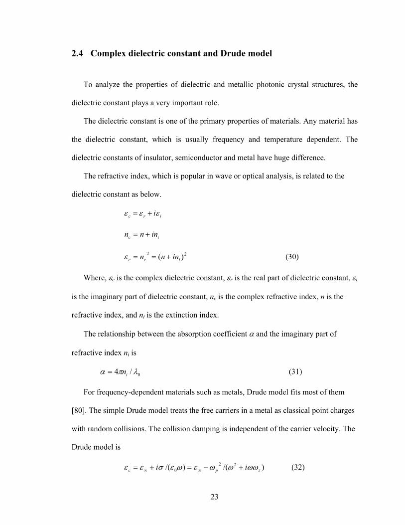
2-1 TM Band structure of 2D square silicon cylinder array (PWE) ............................................................................... 14
2-2 TM Band structure of 2D square
silicon cylinder array (FDTD) ............................................................................. 17
2-3 Transmission coefficient of normal incidence (TM) on 8 columns 2D square silicon cylinder array ................................................... 22
3-1 Some examples of fabrication
for THz photonic crystal structures ..................................................................... 26
3-2 Fabrication of SU-8 photonic crystal structures ..................................................... 28
3-3 SEM picture of SU-8 polymer cylinders on 3 inch Si wafer .................................. 29
3-4 SEM picture of SU-8 polymer holes on 3 inch Si wafer ........................................ 29
3-5 Schematic diagram of Sputtering deposition .......................................................... 31 3-6 Schematic diagram of glancing angle
deposition in the thermal evaporator ................................................................... 32
3-7 Si 1D photonic crystals by dicing ........................................................................... 33
3-8 Si 2D photonic crystals by dicing ........................................................................... 34
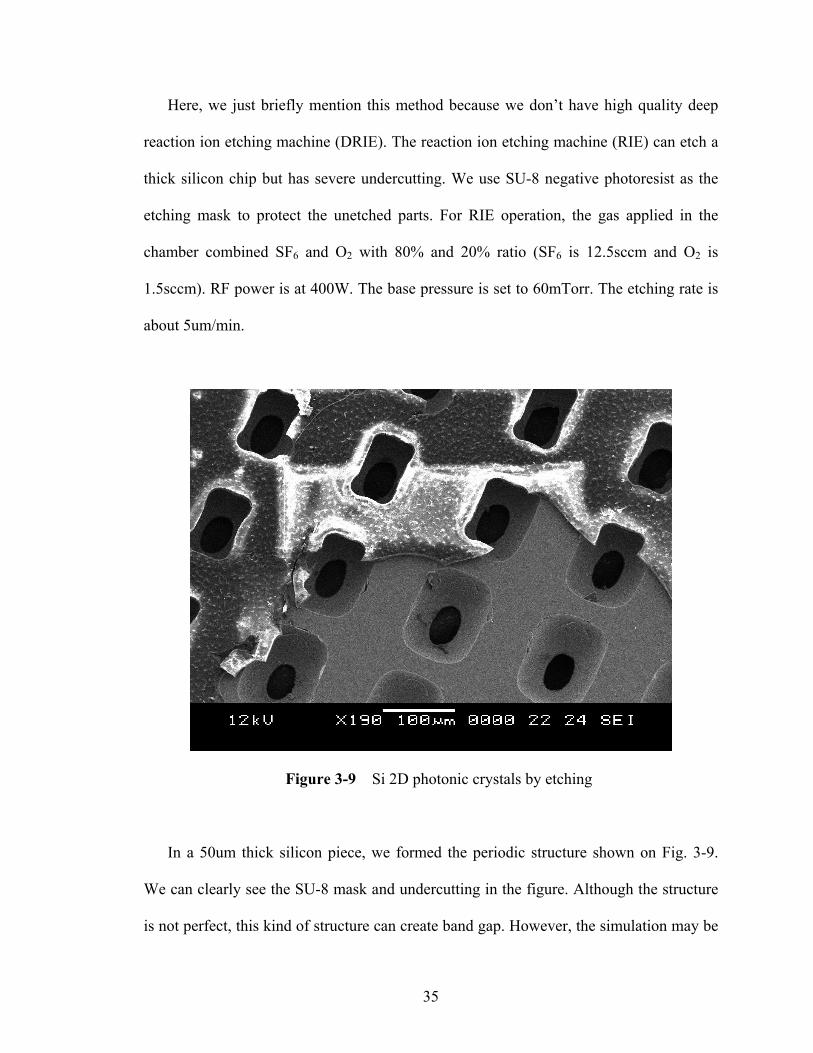
3-9 Si 2D photonic crystals by etching ......................................................................... 35
4-1 Schematic of one sample chip ................................................................................ 38
vi
4-2 SEM picture of part of 4-C chip ............................................................................. 39 4-3 The not-to-scale sideview and 3D view of the setup
of the sample in waveguide coupling by two silicon lenses ................................. 41 4-4 Whole THz-TDS setup with sample
setup in the center of THz path ........................................................................... 43
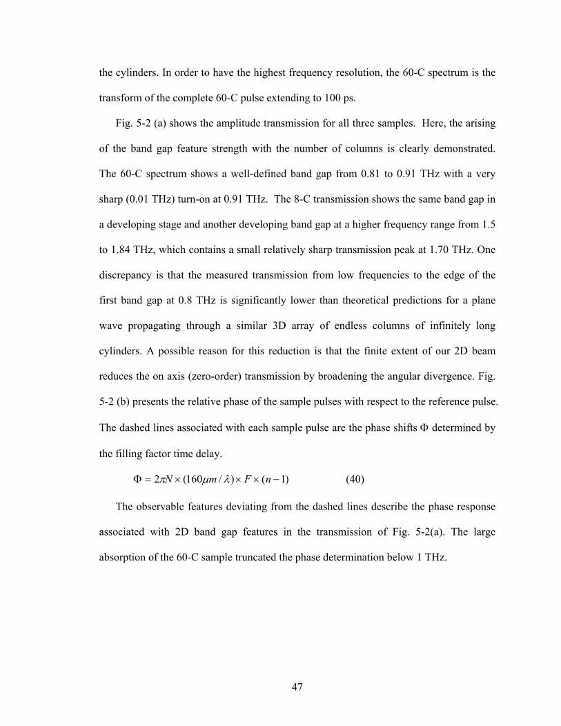
5-1 The measurement results of SU-8 photonic crystals .............................................. 45 5-2 THz-TDS measurement of the 4-C,
8-C and 60-C samples, respectively ................................................................... 48 5-3 Band structure of 2-D square polymer photonic
crystals with a=160µm, d=70µm and infinite height ......................................... 49 5-4 Measured power transmission for the 4-C and 60-C samples
(solid curves) compared with theory (dotted curves) ........................................... 50 5-5 Transmitted THz pulse through the reference sample
and the corresponding amplitude spectrum .......................................................... 54 5-6 Measured 4-C Al (dotted curve), 4-C Au (solid curve)
transmitted THz pulses and spectra, respectively ............................................... 55 5-7 Measured power transmission for the 4-C Au sample
(solid curve) compared with theory (dotted curve) ............................................. 56 5-8 Measured power transmission for the 4-C Al sample
(solid curve) compared with theory (dotted curve) ............................................. 59 5-9 2D and 3D Band diagram of 4-C Au sample
with changing incident angle ............................................................................. 60 5-10 (a) The not-to-scale schematic diagram of
the samples. (b) SEM image of Sample B .............................................................. 62 5-11 Transmitted THz pulse through the Reference Sample
and the corresponding amplitude spectrum ......................................................... 63
5-12 THz-TDS measurement result of Sample A .......................................................... 64
5-13 THz-TDS measurement result of Sample B ........................................................... 66
5-14 THz-TDS measurement result of Sample C ........................................................... 68
vii
6-1 Measured reference THz pulses .............................................................................. 72
6-2 Measured 4-C Au with line defect transmitted THz pulses ..................................... 73
6-3 Measured amplitude transmission for the 4-C Au with line defect sample ............. 74
6-4 Measured power transmission for the 4-C Au with line defect sample ................... 75 6-5 Not to scale schematic diagram showing THz propagation
direction perpendicular to the columns of the array ............................................... 78 6-6 Measured amplitude transmission with the air gap
of 0µm, 15µm, 30µm, 50µm, 75µm, and 100µm, respectively ............................ 80
6-7 Measured amplitude transmission (log scale) with the air gap of 0µm, 15µm, 30µm, 50µm, 75µm, and 100µm, respectively ............................ 81
6-8 The plot of lower and upper band edges
as a function of the air gap from 10µm to 100µm ............................................. 83
viii
LIST OF THE SYMBOLS
α absorption coefficient
ω angular wave frequency
σ complex conductivity
εc complex dielectric constant
σdc dc conductivity
εI imaginary part of dielectric constant
εr real part of dielectric constant
∆ difference, usage as specified in text
1D one-dimensional
2D two-dimensional
3D three-dimensional
a lattice constant
Al aluminum
Au gold
B magnetic flux density
c speed of light in free space (2.998 x 10⁸ m/s)
D electric flux density
e electric charge of an electron
ix
E electric field
Ex Electric field amplitude in x-direction
Ey Electric field amplitude in y-direction
Ez Electric field amplitude in z-direction
FCC face-centered cubic
FDTD finite-difference time-domain
G reciprocal vector
GaAs Gallium Arsenide
GLAD glancing angle deposition
H magnetic field
Hx Magnetic field amplitude in x-direction
Hy Magnetic field amplitude in y-direction
Hz Magnetic field amplitude in z-direction
J current density
k wave vector
kx wave vector in x-direction
ky wave vector in y-direction
kz wave vector in z-direction
LED light-emitting diode
m* effective mass of electron
MEMS micro-electro-mechanical-systems
N free electron density
n real part of refractive index
x
nc complex refractive index
ni imaginary part of refractive index
PBC periodic boundary conditions
PBG photonic band gap
PC photonic crystal
PML perfect matched layer
PPWG parallel plate waveguide
PVD physical vapor deposition
PWE plane wave expansion
R basis vector or primitive lattice vector
RIE reactive ion etching
SEM scanning electron microscope
Si Silicon
t time
T transfer matrix
TE transverse electric
TEM transverse electromagnetic
THz terahertz
THz-TDS terahertz time-domain spectroscopy
TM transverse magnetic
TMM transfer matrix method
UV ultra violet
ε relative permittivity (dielectric constant)
xi
ε0 permittivity of vacuum, 8.85 × 10⁻¹² F/m
λ wavelength in free space
µ relative permeability
µ0 Permeability of vacuum, 4π × 10-7 H/m
τ carrier collision time
φ phase angle, usage as specified in text (radians)
ωτ damping frequency
ωp plasma frequency
xii
CHAPTER I
INTRODUCTION
The photonic crystal concept is originally from the solid state physics. As we all
know, semiconductors have become very important materials in our daily life. The most
critical property of a semiconductor is its energy gap or band structure. From the crystal
structure map of a semiconductor such as a face-centered cubic lattice (FCC), we can see
that the atoms are periodically arranged. Because of the periodic potential in this structure,
the electrons can only occupy some certain energy bands that are separated by forbidden
gaps. The energy versus effective momentum (E-k) relation shows the gaps very clearly.
Analogically, if a material has periodic structure in space, a band structure is expected.
The study of periodic structured material can be traced to the nineteen century. Lord
Rayleigh did some electromagnetic wave propagation experiments in one-dimensional
media. In 1987, E. Yablonovitch and S. John proposed the concept of photonic crystals to
summarize the periodic structured materials [1, 2]. Since then, the artificial photonic
crystals have been studied intensively and great progress has been achieved. The
developments of theories, experiments, fabrication techniques and applications of
photonic crystals not only exist in the microwave and optical regions, but also extend to
the infrared and far-infrared region, which includes the terahertz range.
1
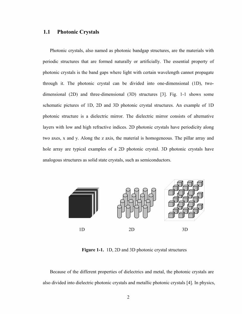
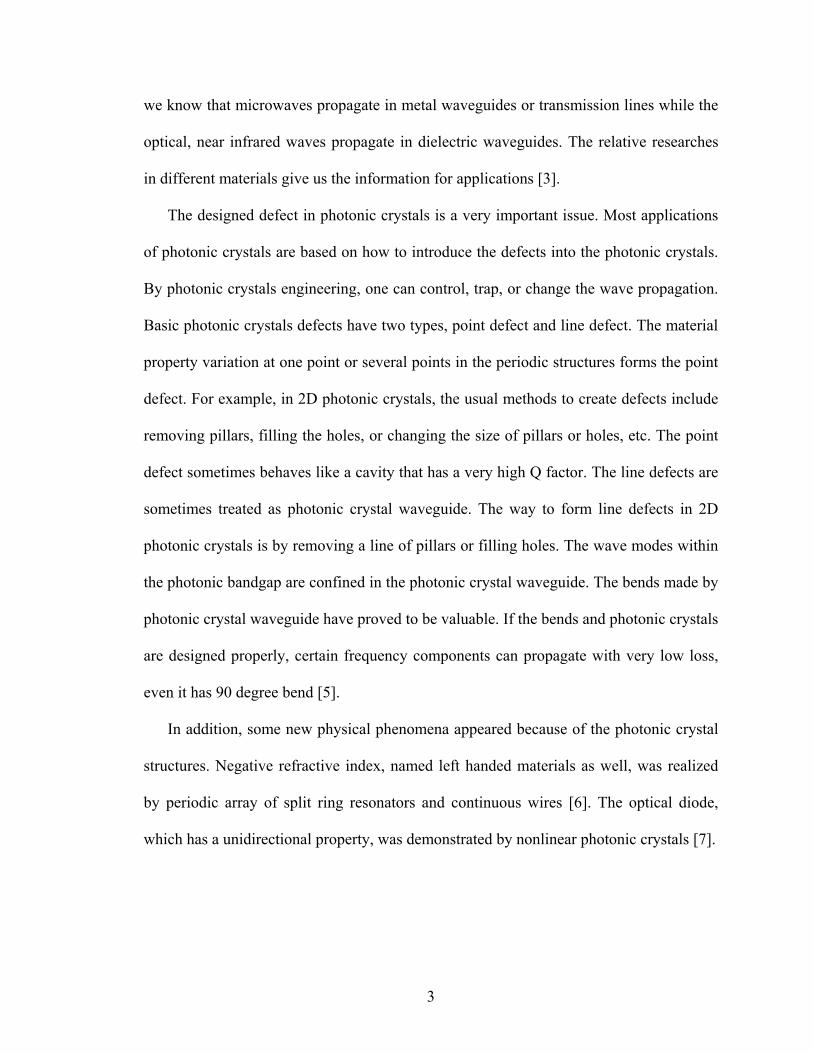
1.1 Photonic Crystals
Photonic crystals, also named as photonic bandgap structures, are the materials with
periodic structures that are formed naturally or artificially. The essential property of
photonic crystals is the band gaps where light with certain wavelength cannot propagate
through it. The photonic crystal can be divided into one-dimensional (1D), two-
dimensional (2D) and three-dimensional (3D) structures [3]. Fig. 1-1 shows some
schematic pictures of 1D, 2D and 3D photonic crystal structures. An example of 1D
photonic structure is a dielectric mirror. The dielectric mirror consists of alternative
layers with low and high refractive indices. 2D photonic crystals have periodicity along
two axes, x and y. Along the z axis, the material is homogeneous. The pillar array and
hole array are typical examples of a 2D photonic crystal. 3D photonic crystals have
analogous structures as solid state crystals, such as semiconductors.
1D 2D 3D
Figure 1-1. 1D, 2D and 3D photonic crystal structures
Because of the different properties of dielectrics and metal, the photonic crystals are
also divided into dielectric photonic crystals and metallic photonic crystals [4]. In physics,
2
we
o the photonic crystals.
By
ndex, named left handed materials as well, was realized
by
know that microwaves propagate in metal waveguides or transmission lines while the
optical, near infrared waves propagate in dielectric waveguides. The relative researches
in different materials give us the information for applications [3].
The designed defect in photonic crystals is a very important issue. Most applications
of photonic crystals are based on how to introduce the defects int
photonic crystals engineering, one can control, trap, or change the wave propagation.
Basic photonic crystals defects have two types, point defect and line defect. The material
property variation at one point or several points in the periodic structures forms the point
defect. For example, in 2D photonic crystals, the usual methods to create defects include
removing pillars, filling the holes, or changing the size of pillars or holes, etc. The point
defect sometimes behaves like a cavity that has a very high Q factor. The line defects are
sometimes treated as photonic crystal waveguide. The way to form line defects in 2D
photonic crystals is by removing a line of pillars or filling holes. The wave modes within
the photonic bandgap are confined in the photonic crystal waveguide. The bends made by
photonic crystal waveguide have proved to be valuable. If the bends and photonic crystals
are designed properly, certain frequency components can propagate with very low loss,
even it has 90 degree bend [5].
In addition, some new physical phenomena appeared because of the photonic crystal
structures. Negative refractive i
periodic array of split ring resonators and continuous wires [6]. The optical diode,
which has a unidirectional property, was demonstrated by nonlinear photonic crystals [7].
3
WAVEGUIDEFILTER
LED
Photonic Crystals
SWITCHING POLARIZER
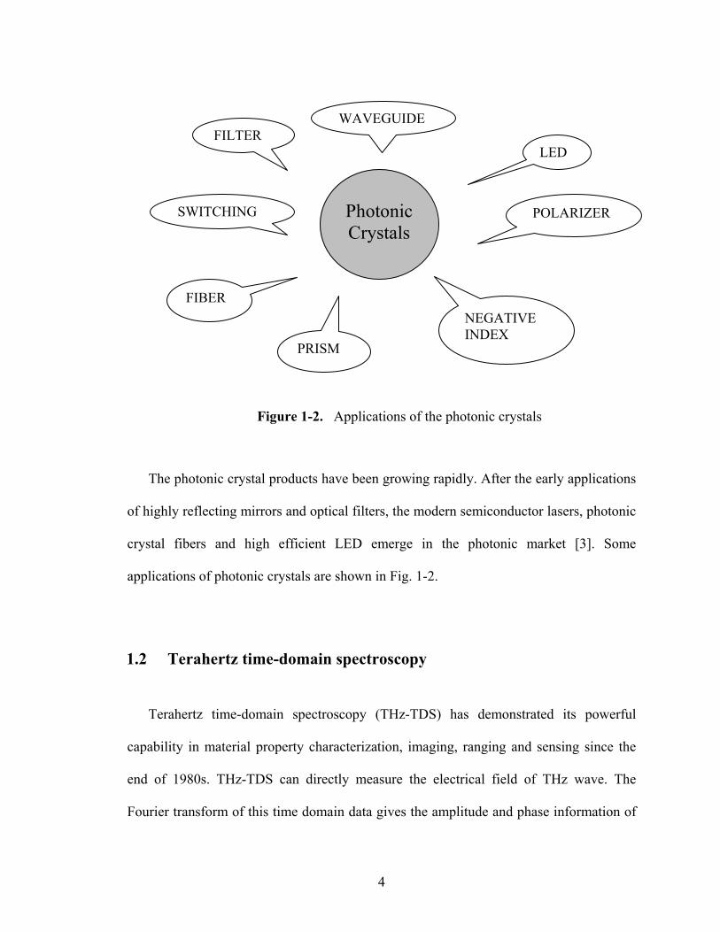
Figure 1-2. Applications of the photonic crystals
The photonic crystal products have been growing rapidly. After the early applications
of highly reflecting mirrors and optical filters, the modern semiconductor lasers, photonic
crystal fibers and high efficient LED emerge in the photonic market [3]. Some
applications of photonic crystals are shown in Fig. 1-2.
1.2 Terahertz time-domain spectroscopy
Terahertz time-domain spectroscopy (THz-TDS) has demonstrated its powerful
capability in material property characterization, imaging, ranging and sensing since the
end of 1980s. THz-TDS can directly measure the electrical field of THz wave. The
Fourier transform of this time domain data gives the amplitude and phase information of
NEGATIVE INDEX
FIBER
PRISM
4
the THz wave pulse, therefore, providing the wideband spectrum and the real and
imaginary parts of the dielectric constant. This also allows precise measurements of the
refractive index and absorption coefficient of samples [8, 9].
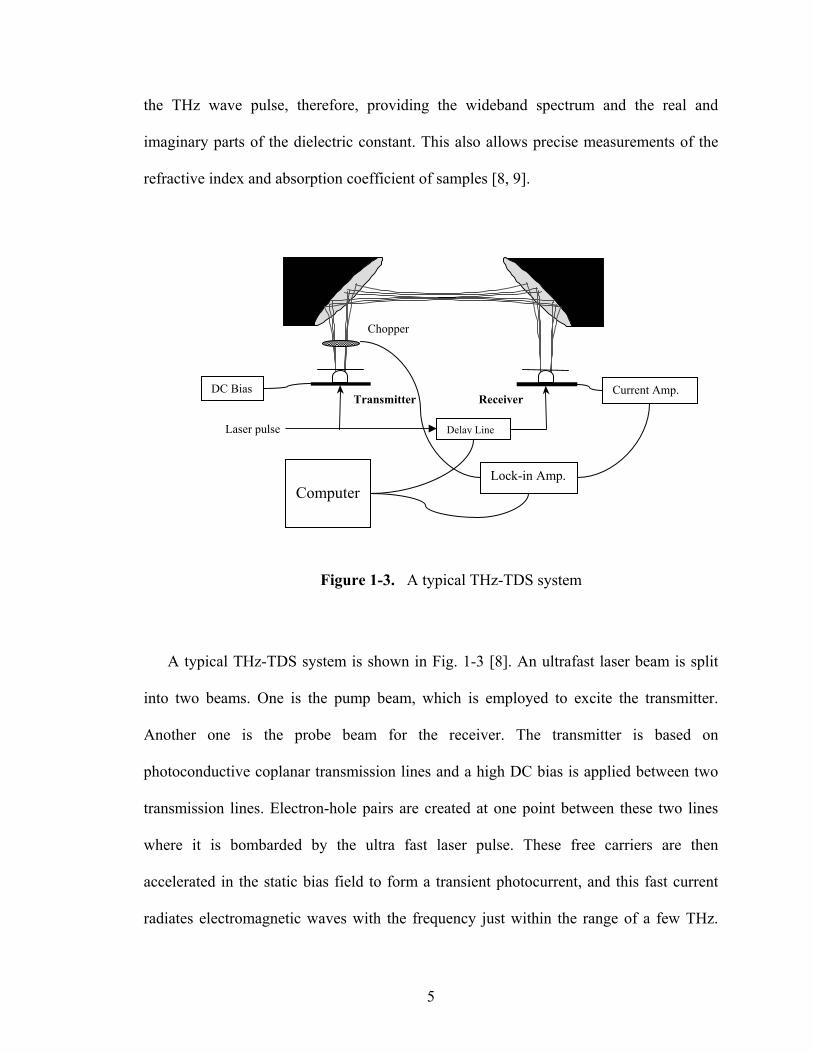
Figure 1-3. A typical THz-TDS system
A typical THz-TDS system is shown in Fig. 1-3 [8]. An ultrafast laser beam is split
into two beams. One is the pump beam, which is employed to excite the transmitter.
Another one is the probe beam for the receiver. The transmitter is based on
photoconductive coplanar transmission lines and a high DC bias is applied between two
transmission lines. Electron-hole pairs are created at one point between these two lines
where it is bombarded by the ultra fast laser pulse. These free carriers are then
accelerated in the static bias field to form a transient photocurrent, and this fast current
radiates electromagnetic waves with the frequency just within the range of a few THz.
Laser pulse
ReceiverTransmitter
Chopper
DC Bias Current Amp.
Lock-in Amp. Computer
Delay Line
5
The THz radiation is collected by silicon lens that are attached on the back of chip, and
then collimated by a paraboloidal mirror. Through the same structure with a paraboloidal
mirror and silicon lens, the freely propagating THz radiation is collected by the receiver.
The probe laser beam triggers the receiver’s photo conductive switch and creates the
current proportional to the amplitude of THz radiation received by the chip. By changing
the path length of the probe laser beam, the time domain THz radiation pulse can be
measured. The photo conductive switch is just like a sampling gate that opens for just
several hundreds femtosecond signals. In this way, it is easy to get a THz pulse of time
domain, as well as the frequency domain information by a Fourier transformation [8].
1.3 Progress in photonic crystals research in microwave and THz
range
In order to understand the accomplishment and significance of the work presented in
this thesis, we first review the microwave and THz experimental work on photonic
crystals. This review section is similar to the review in Ref. 9. It is especially important to
connect the recent THz work to the extensive microwave literature, because all of the
THz guided wave demonstrations have their microwave counterparts, and because for
both THz and microwaves the real part of the conductivity can be considered to be
frequency independent and to be equal to the handbook dc value, in contrast to metallic
conductivity at optical frequencies. Photonic crystals in the microwave and THz range
6
have been studied both experimentally [10-46], and theoretically [47-66] for more than a
decade. Compared to microwaves, THz phenomena occur at a smaller spatial scale
proportional to their shorter wavelengths. The corresponding frequency dependent losses
are higher and the skin depths are smaller, but the basic phenomena are the same. The
smaller THz spatial scale is especially convenient for the use of quasi-optics and
associated techniques.
In contrast to the optical frequency range [67, 68], where submicron technology is
needed to fabricate photonic structures, the microwave range allows for precise hand-
assembly of photonic crystals composed of identical mm to cm sized components on
repetitive lattice spacings with similar dimensions [10-46]. Most microwave photonic
crystals have consisted of arrays of dielectric or metal spheres, arrays of cylinders, or
arrays of square rods, sometimes supported by dielectric templates. These techniques
have enabled the construction and experimental characterization of both two-dimensional
(2D) [12-16, 23, 26, 29, 32, 34, 35, 37] and three-dimensional (3D) [17, 18, 20-22, 24,
25, 28, 33, 36, 43] photonic crystals. Typical photonic crystals are of the order of 10
lattice spacings long by 20 spacings wide with lattice spacings of the order of the
wavelength. Although point source excitation and detection of the transmitted
microwaves through the 3D photonic crystal was initially used with excellent results [11],
more commonly, the crystals were characterized by input microwave beams with
diameters smaller than the input face of the photonic crystal and radii of curvatures of
several times the beam diameters. The first and quite notable 3D microwave
characterization of photonic crystals [10, 11], reported the observation of a photonic
band-gap between 13 and 16 GHz with a dynamic range of 50 dB and narrow donor and
7
acceptor modes with a dynamic range of 20 dB in a Yablonovitch type crystal made of
Stycast dielectric. Ozbay’s later approach of an orderly stacking of dielectric rods to
fabricate 3D photonic crystals [17, 18], also enabled measurements of 3D photonic
bandgaps between 12 and 14 GHz with a dynamic range of 50 dB and the observation of
sharp defect structures with a dynamic range of 20 dB. Later the same approach, using
metal rods, demonstrated a photonic bandgap with a dynamic range of 70 dB as well as a
sharp defect line at 17.22 GHz with a dynamic range of 15 dB and a FWHM linewidth of
0.03 GHz [25].
The first precise microwave characterization of a 2D dielectric photonic crystal was
reported in Ref. 12. The photonic crystal consisted of a 9 x 18 array of 1 cm long, 0.96
cm diameter alumina-composite cylinders on a square lattice with lattice constant 1.27
cm, as determined by a numerically drilled Styrofoam template. This structure was
installed into a wide 2D parallel plate scattering chamber tapering to 8-12 GHz
waveguide ports on each end. Here well defined photonic bandgaps were observed
between 10 and 12 GHz with a dynamic range of 20 dB. Also, a sharp peak at 11.2 GHz
was observed with a dynamic range of 10 dB due to a localized defect. An important
advance at higher frequencies was the characterization from 15 to 150 GHz by Robertson
[13] of a 2D dielectric array of long alumina-ceramic rods arranged in a square lattice.
This measurement was made by transmitting the freely propagating and collimated beam
from an optoelectronic source through the array. Photonic bandgaps were observed from
50 to 75 GHz with a dynamic range of 26 dB. Later work [23] with a 2D photonic crystal
consisting of 10 cm long, 0.51 mm diameter cylinders of alumina-ceramic arranged in a
square lattice with a lattice constant of 1.27 mm showed a deep photonic bandgap from
8
75-110 GHz. By removing two layers of cylinders from the middle of the photonic
crystal, a quantum well type structure of barrier-well-barrier was produced [23]. For an
optimum thickness of the barriers at 14 layers of cylinders, the quasi-bound state of the
cavity was observed at 85.48 GHz with a linewidth of only 3.5 MHz corresponding to a
cavity Q with the extraordinary value of 2.3 x 10⁴ [23].
The photonic crystal research in THz region can be dated back to the early of 90’s.
The first 3D THz photonic crystal construction and characterization is described in Ref.
19. In this work, the crystal, built by the orderly stacking of dielectric rods, showed a
photonic bandgap from 370 to 520 GHz with a dynamic range of 30 dB. In several years,
the researches in terahertz region become more and more active. The subsequent THz
characterization of a 2D metallic photonic crystal, consisting of a 2D honeycomb of
metal 80 µm diameter cylinders threaded through two brass supporting meshes separated
by 3 cm, was reported in Ref. 29. The measured transmission showed strong frequency
dependence from 0.8 to 1.7 THz with a dynamic range of 10 dB. Another work measured
THz phase shifts in a 2D photonic crystal fabricated by drilling holes in a methylpentene
polymer [32]. Deep X-ray lithography has been used to fabricate 2D metallic photonic
crystals, consisting of square and triangular lattices of nickel pillars [35]. For the square
lattice of nickel pillars with a diameter of 26.4 µm and a lattice constant of 60 µm,
transmission variations of 3 dB were observed from 1 to 6 THz [35]. In another THz
experiment [38], metal 2D photonic crystals were constructed with nickel coated, 50 µm
diameter silica cylinders confined and aligned between two parallel 70 µm square array
brass meshes. Relatively sharp features were observed with the 2D crystal lattice constant
of 140 µm. For a crystal length of 10 periods a 90 dB attenuation feature observed at 2.2
9
THz was identified as the center frequency of the photonic bandgap [38]. A THz 2D
photonic crystal has been fabricated and characterized as a “Terahertz plasmonic high
pass filter” [39]. This crystal was fabricated by layer-by-layer photopolymerization of
UV curable resin, whereby the desired cross-section pattern was projected in UV light
onto the resin. The resulting 2D photonic crystal consisted of 1 mm long, 30 µm diameter
cylinders on a 120 µm square lattice, covered with a thin film of sputtered gold. The THz
reflectivity was measured from 0.5 to 6 THz [39]. Deep reactive ion etching has also
been used to fabricate a 2-D THz photonic crystal [40]. Here, 80 µm square holes on a
100 µm square lattice were etched through a 500 µm thick, high resistivity Si wafer. The
resulting 2D slab waveguide showed a photonic bandgap from 0.9 to 1.2 THz with a
dynamic range of 13 dB [40]. Recent work by Mittleman [42] has reported THz
transmission studies of a hexagonal array of 360 µm diameter air holes with a 400 µm
lattice constant in a 300 µm thick, high-resistivity silicon slab within a parallel plate
metal waveguide. The THz-TDS characterization from 0.2 to 0.4 THz showed photonic
bandgap features together with an observable defect mode in qualitative agreement with
the transfer matrix method theory [47, 55].
Besides the investigation in theories and experiments, several groups also conduct
research in some application areas. Frequency filtering is a basic application of photonic
crystals due to the essential bandgap property. The general filter [69], high-pass filter
[70] and tunable filter [71] are demonstrated in THz frequencies. The other applications
include photonic crystal lens [72], photonic crystal waveguide [73], photonic fibers [74],
THz generation [75], and biochemical sensing [76].
10
1.4 About this thesis
In this thesis, the study of THz photonic crystal structures will be discussed
including theories, fabrication, experiments, and applications. Chapter 2 describes the
theories of band structure of photonic crystals, the methods to calculate the photonic
crystals and the Drude model of material that is used in analysis. Chapter 3 talks about
the fabrication of the Micro-Electro-Mechanical-Systems (MEMS) with lithography
method, as well as the back-end process, such as dicing. Chapter 4 describes the setup of
our experiment system and the advantage of the setup. Chapter 5 shows and explains the
results of a series of basic photonic crystal experiments. The results of the SU-8 (polymer)
photonic crystals, metallic photonic crystals and metallic photonic crystals with defects
are demonstrated and compared to the computation results. The good agreement indicates
the success of experiment setup and sample quality. Chapter 6 discusses some
applications of the THz photonic crystals. THz photonic crystal waveguide and tunable
photonic bandgap structures are realized and demonstrated. Chapter 7 summarizes the
whole thesis.
11
CHAPTER II
RELATED THEORIES
2.1 Basic analysis of photonic crystals
The fundamental theory of the band structure of photonic crystals is Maxell’s
equations. First, we need to know how the field in the media is determined.
Faraday’s law: tBE∂∂
−=×∇v
r (1)
Ampere’s law: tDJH∂∂
+=×∇v
vv (2)
For a source free field,
0=Jv
HBvv
0µ= (µ=1 for most materials)
and EDvv
0εε=
And we assume the field has harmonic time dependence, tie ω−
HiEvr
0ωµ=×∇ (3)
EiHvv
0ωεε−=×∇ (4)
12
We know the speed of light00
1µε
=c , from (3) and (4), we get
Hc
Hvv
2
2
)1( ωε
=×∇×∇ (5)
Consider (5) plus the condition 0=⋅∇ Hv
, we can solve this eigenvalue problem and
find Hv
. In addition, Ev
can be obtained from (4). [3]
But the solutions of the fields are not enough. There are mainly three supporting
concepts used in band structure calculation of photonic crystals, Bloch’s theorem, the
reciprocal lattice and the Brillouin zone.
In typical photonic crystals, the materials are periodically distributed. We have ε(r)
=ε(r+a), and here a is the periodic constant. Bloch’s theorem states the wave in such
material governed by a periodic envelope function multiplied by a plane wave. So the
solution of (5) can be chosen as )()( , xHexH knikx vv
= with eigenvalue ωn(k).
The reciprocal lattice describes a function such as f(r)=f(r+R) in the periodic lattice
induces exp(iG⋅R)=1. The vector G, which defined by G⋅R=n2π, is called reciprocal
vector. The basis vectors in the lattice are R1, R2 and R3, which are also termed as
primitive lattice vectors. The reciprocal lattice vectors are defined by:
321
321 2
RRRRRGו
×= π (6)
321
132 2
RRRRRGו
×= π (7)
321
213 2
RRRRRGו
×= π (8)
13
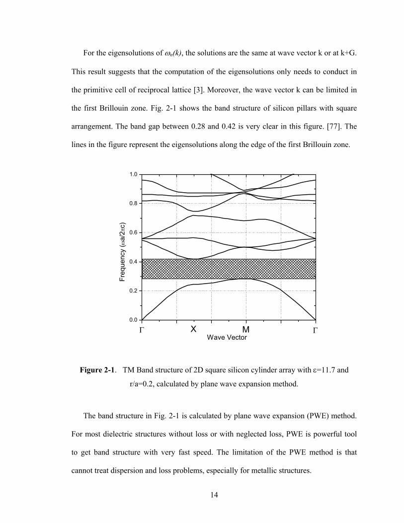
For the eigensolutions of ωn(k), the solutions are the same at wave vector k or at k+G.
This result suggests that the computation of the eigensolutions only needs to conduct in
the primitive cell of reciprocal lattice [3]. Moreover, the wave vector k can be limited in
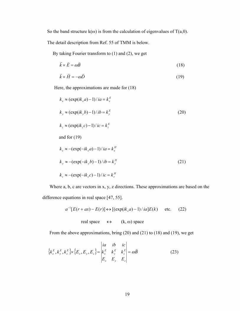
the first Brillouin zone. Fig. 2-1 shows the band structure of silicon pillars with square
arrangement. The band gap between 0.28 and 0.42 is very clear in this figure. [77]. The
lines in the figure represent the eigensolutions along the edge of the first Brillouin zone.
0.0
0.2
0.4
0.6
0.8
1.0
X M ΓΓ
Freq
uenc
y (ω
a/2π
c)
Wave Vector
Figure 2-1. TM Band structure of 2D square silicon cylinder array with ε=11.7 and
r/a=0.2, calculated by plane wave expansion method.
The band structure in Fig. 2-1 is calculated by plane wave expansion (PWE) method.
For most dielectric structures without loss or with neglected loss, PWE is powerful tool
to get band structure with very fast speed. The limitation of the PWE method is that
cannot treat dispersion and loss problems, especially for metallic structures.
14
The calculation methods of band structure have been developed very fast in recent
years and many practical theories are proved by many experiments. The main methods
not only include PWE method [77], but also include the multi-scattering method, the
transfer matrix method (TMM) [47, 55, 65], the finite difference time domain (FDTD)
method [63, 64, 78] and so on. Each method has its advantages in solving certain types of
band structure. Among these methods, FDTD and TMM are the most popular methods.
2.2 Finite Difference Time Domain (FDTD) method
In 1966, Kane S. Yee introduced this method [78], since then FDTD become very
popular method to solve various electromagnetic problems, which include photonic
crystal problems.
FDTD method is direct solution from Maxwell’s time dependent curl equations.
µ1)(
zE
yE
tH yzx
∂
∂−
∂∂
−=∂∂ (9)
µ1)(
xE
zE
tH zxy
∂∂
−∂∂
−=∂∂
(10)
µ1)(
xE
yE
tH yxz
∂
∂−
∂∂
=∂∂ (11)
ε1)(
zH
yH
tE yzx
∂∂
−∂∂
=∂∂ (12)
ε1)(
xH
zH
tE zxy
∂∂
−∂∂
=∂∂
(13)
15
ε1)(
yH
xH
tE xyz
∂∂
−∂
∂=
∂∂ (14)
Then the finite differential equations are constructed according to (9) to (14).
y
kjiEkjiE
z
kjiEkjiE
t
kjiHkjiH
nz
nz
ny
ny
nx
nx
∆
+−++−
∆
+−++=
∆
++−++ −+
µ
µ
)21,,()
21,1,(
),21,()1,
21,()
21,
21,()
21,
21,( 2/12/1
(15)
z
kjiHkjiH
y
kjiHkjiH
t
kjiEkjiE
ny
ny
nz
nz
nx
nx
∆
−+−++−
∆
−+−++=
∆
+−+
−−
−−−
ε
ε
)21,,
21()
21,,
21(
),21,
21(),
21,
21(),,
21(),,
21(
2/12/1
2/12/11
(16)
(15) and (16) are differential equations of Hx and Ex. Other equations can be obtained
by exchanging the x, y and z subscripts. The differential equations are divided into finite
difference equivalents in a grid of space ∆x, ∆y, and ∆z, and time nodes ∆t. One
equivalent in one grid point is related to the neighbor grid point.
To numerically simulate the results, some numerical parameters are required. For
basic FDTD problem, a finite domain, a boundary condition, and spatial and temporal
grids are defined before the simulation. Perfect matched layer (PML) is the most common
boundary condition FDTD method used. Both electric and magnetic conductivities
remains constant at PML and the energy is absorbed without reflection. However,
periodic boundary conditions (PBC) are employed for photonic crystal simulation. PBC
is chosen to ensure the equivalent infinite repeated structures. The spatial and temporal
16
grids are chosen small enough to produce accurate simulation. The stability of simulation
depends on the relationship of spatial and temporal grids.
tczyx
∆>∆+∆+∆ 222 )/1()/1()/1(
1 (17)
The denser the grid points in the FDTD problem, the more exact solutions it has. The
time and memory consuming will increase significantly as well with small grid. The
development of various FDTD methods allows calculating some complicated cases such
as metallic or metallo-dielectric photonic crystals [63, 64].
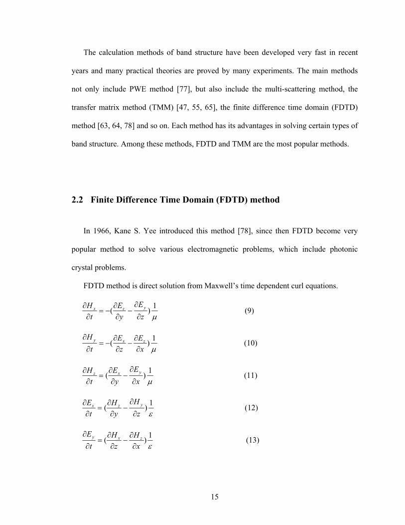
0.0
0.2
0.4
0.6
0.8
1.0
MX ΓΓ
Freq
uenc
y (ω
a/2π
c)
Wave Vector
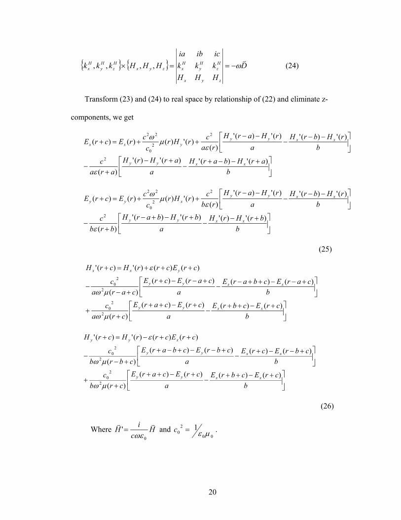
Figure 2-2. TM Band structure of 2D square silicon cylinder array with ε=11.7 and
r/a=0.2, calculated by FDTD method.
17
Fig. 2-2 gives a band structure example of the same 2D Si photonic crystals as Fig. 2-
1. It shows that there is same band gap between 0.28(c/a) to 0.42(c/a).
There are some commercial softwares (such as Rsoft) and free softwares (such as F2P)
available to calculate and design photonic crystals.
2.3 Transfer Matrix Method (TMM)
Transfer Matrix Method for photonic crystals calculation is developed by J.B. Pendry
et. al. [47]. This method can handle most photonic crystal structures, including the
photonic crystal defects and the metallic photonic crystals [55].
Given the field in one point, let’s say at (x1, y1, z1), by solving the Maxwell’s
equations, the field in another point at (x2, y2, z2) can be calculated when they are in the
same space and other conditions such as materials are known. If we make it a little simple
and suppose the x and y are fixed, only the z changes from 0 to a.
If at z=0 ),,,()0( HyHxEyExzF ==
and at z=a ),,,()( HyHxEyExazF ==
We get
)0()0,()( === zFaTazF
Here T is defined as transfer matrix.
T(a,0) can be treated as a matrix of combining of transmission and reflection
coefficients in photonic system. In photonic crystals, because of the periodic structures,
we can apply the Bloch condition in this equation.
)0()0,()()0( )( ===== zFaTazFezF aik ω So, aikeaT )()0,( ω=
18
So the band structure k(ω) is from the calculation of eigenvalues of T(a,0).
The detail description from Ref. 55 of TMM is below.
By taking Fourier transform to (1) and (2), we get
(18) BEkvvv
ω=×
DHkvvv
ω−=× (19)
Here, the approximations are made for (18)
Exxx kiaaikk =−≈ /)1)(exp(
Eyyy kibbikk =−≈ /)1)(exp( (20)
Ezzz kiccikk =−≈ /)1)(exp(
and for (19)
Hxxx kiaaikk =−−−≈ /)1)(exp(
Hyyy kibbikk =−−−≈ /)1)(exp( (21)
Hzzz kiccikk =−−−≈ /)1)(exp(
Where a, b, c are vectors in x, y, z directions. These approximations are based on the
difference equations in real space [47, 55].
)(]/)1)[(exp()]()([1 kEiaaikrEaxrEa x −↔−+− etc. (22)
real space ↔ (k, ω) space
From the above approximations, bring (20) and (21) to (18) and (19), we get
BEEEkkkicibia
EEEkkk
zyx
Ez
Ey
Exzyx
Ez
Ey
Ex
vω==× ,,,, (23)
19
DHHHkkkicibia
HHHkkk
zyx
Hz
Hy
Hxzyx
Hz
Hy
Hx
vω−==× ,,,, (24)
Transform (23) and (24) to real space by relationship of (22) and eliminate z-
components, we get
⎥⎦
⎤⎢⎣
⎡ +−−+−
+−
+−
⎥⎦
⎤⎢⎣
⎡ −−−
−−++=+
barHbarH
aarHrH
arac
brHbrH
arHarH
racrHr
ccrEcrE
xxyy
xxyyyxx
)(')(')(')(')(
)(')(')(')(')(
)(')()()(
2
2
20
22
ε
εµω
⎥⎦
⎤⎢⎣
⎡ +−−
+−+−
+−
⎥⎦
⎤⎢⎣
⎡ −−−
−−++=+
bbrHrH
abrHbarH
brbc
brHbrH
arHarH
rbcrHr
ccrEcrE
xxyy
xxyyxyy
)(')(')(')(')(
)(')(')(')(')(
)(')()()(
2
2
20
22
ε
εµω
(25)
⎥⎦
⎤⎢⎣
⎡ +−++−
+−++
++
⎥⎦
⎤⎢⎣
⎡ +−−++−−
+−−+
+−−
+++=+
bcrEcbrE
acrEcarE
crac
bcarEcbarE
acarEcrE
carac
crEcrrHcrH
xxyy
xxyy
yxx
)()()()()(
)()()()()(
)()()(')('
2
20
2
20
µω
µω
ε
⎥⎦
⎤⎢⎣
⎡ +−++−
+−++
++
⎥⎦
⎤⎢⎣
⎡ +−−+−
+−−+−+
+−−
++−=+
bcrEcbrE
acrEcarE
crbc
bcbrEcrE
acbrEcbarE
cbrbc
crEcrrHcrH
xxyy
xxyy
xyy
)()()()()(
)()()()()(
)()()(')('
2
20
2
20
µω
µω
ε
(26)
Where Hc
iHvv
0
'ωε
= and 00
20
1µε=c .
20
So if we know the E and H field on one side of the structure, from above equations,
the field on the other side can be decided.
The transfer matrix is
(27)
⎥⎥⎥⎥⎥
⎦
⎤
⎢⎢⎢⎢⎢
⎣
⎡
⎥⎥⎥⎥
⎦
⎤
⎢⎢⎢⎢
⎣
⎡
=
⎥⎥⎥⎥⎥
⎦
⎤
⎢⎢⎢⎢⎢
⎣
⎡
++
++
∑)'()'()'()'(
)',()',()',()',()',()',()',()',()',()',()',()',()',()',()',()',(
)()(
)()(
'
44434241
34333231
24232221
14131211
rHrHrErE
rrTrrTrrTrrTrrTrrTrrTrrTrrTrrTrrTrrTrrTrrTrrTrrT
crHcrH
crEcrE
y
x
y
x
r
y
x
y
x
For photonic crystals, the periodicity is L*c, so
(28)
⎥⎥⎥⎥⎥
⎦
⎤
⎢⎢⎢⎢⎢
⎣
⎡
=
⎥⎥⎥⎥⎥
⎦
⎤
⎢⎢⎢⎢⎢
⎣
⎡
++
++
∑)'()'()'()'(
)0,(
)()(
)()(
'
rHrHrErE
LT
LcrHLcrH
LcrELcrE
y
x
y
x
r
y
x
y
x
where ∏=
−=L
j
jjTLT1
)1,()0,(
Apply Bloch’s theorem,
(29)
⎥⎥⎥⎥⎥
⎦
⎤
⎢⎢⎢⎢⎢
⎣
⎡
=
⎥⎥⎥⎥⎥
⎦
⎤
⎢⎢⎢⎢⎢
⎣
⎡
∑)()()()(
)exp(
)'()'()'()'(
)0,('
rHrHrErE
LaiK
rHrHrErE
LT
y
x
y
x
z
y
x
y
x
r
At a given frequency, we can calculate the eigenvalues and get the entire Bloch wave.
The advantage of TMM is that the calculation is from a given frequency to find the field
and corresponding coefficients. Because the dielectric constant is fixed at a given
frequency, this makes calculation of the frequency dependent materials very simple.
21
0 0.1 0.2 0.3 0.4 0.5 0.6 0.7 0.8 0.9 10
0.1
0.2
0.3
0.4
0.5
0.6
0.7
0.8
0.9
1
Normalized Frequency fa/c
Tran
smis
sion
Coe
ffici
ent
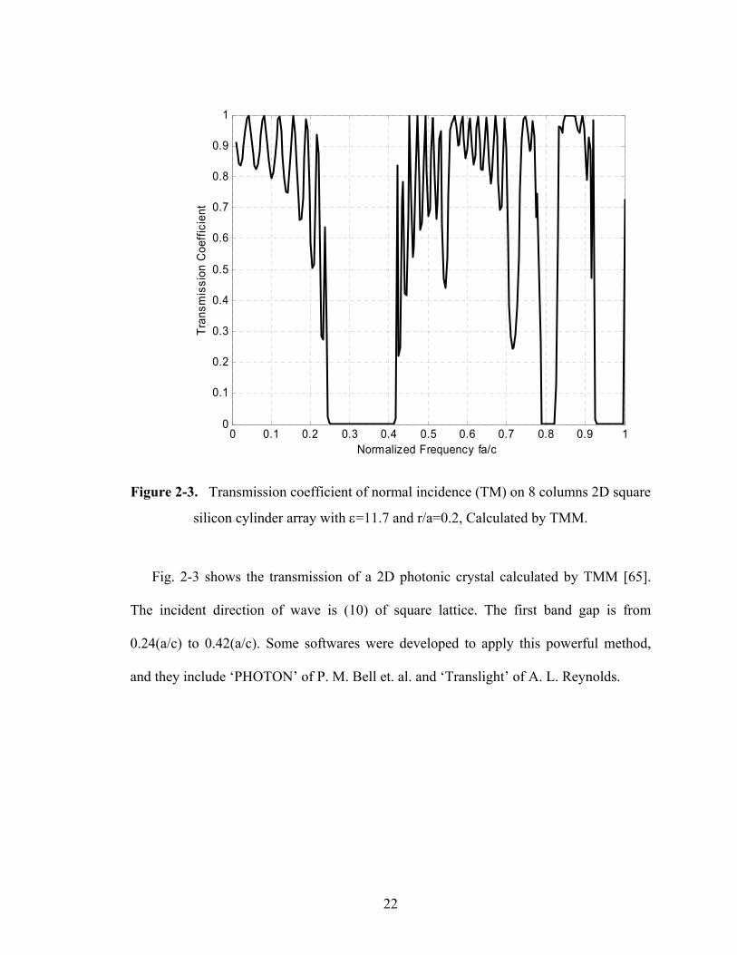
Figure 2-3. Transmission coefficient of normal incidence (TM) on 8 columns 2D square
silicon cylinder array with ε=11.7 and r/a=0.2, Calculated by TMM.
Fig. 2-3 shows the transmission of a 2D photonic crystal calculated by TMM [65].
The incident direction of wave is (10) of square lattice. The first band gap is from
0.24(a/c) to 0.42(a/c). Some softwares were developed to apply this powerful method,
and they include ‘PHOTON’ of P. M. Bell et. al. and ‘Translight’ of A. L. Reynolds.
22
2.4 Complex dielectric constant and Drude model
To analyze the properties of dielectric and metallic photonic crystal structures, the
dielectric constant plays a very important role.
The dielectric constant is one of the primary properties of materials. Any material has
the dielectric constant, which is usually frequency and temperature dependent. The
dielectric constants of insulator, semiconductor and metal have huge difference.
The refractive index, which is popular in wave or optical analysis, is related to the
dielectric constant as below.
irc iεεε +=
ic innn +=
22 )( icc innn +==ε (30)
Where, εc is the complex dielectric constant, εr is the real part of dielectric constant, εi
is the imaginary part of dielectric constant, nc is the complex refractive index, n is the
refractive index, and ni is the extinction index.
The relationship between the absorption coefficient α and the imaginary part of
refractive index ni is
0/4 λπα in= (31)
For frequency-dependent materials such as metals, Drude model fits most of them
[80]. The simple Drude model treats the free carriers in a metal as classical point charges
with random collisions. The collision damping is independent of the carrier velocity. The
Drude model is
)/()/( 220 τωωωωεωεσεε ii pc +−=+= ∞∞ (32)
23
ε∞ is the high frequency dielectric constant and is the contribution of the bound
electrons.
ωp is the plasma frequency of materials. It is a basic parameter of materials.
2/1*
2
)(∞
=ε
ωmNe
p (33)
N is the free electron density, e is electron charge, m* is the effective mass of
electrons, and c is the velocity of light.
ωτ is the damping frequency.
τ
ωτ1
= (34)
τ is the electron lifetime.
23
3
τωωωω
εε+
−= ∞p
r (35)
23
2
τ
τ
ωωω
ωωε
+= p
i (36)
The complex conductivity can be given by
(37) )/()/( 20 τττ ωωωεωωωσσ iiii pdc +=+=
The plasma frequency and damping frequency are usually fixed for the materials. If
the absorption coefficient or refractive index with frequency dependence can be
measured, the measurement results can be compared with the theoretical results [79].
24
CHAPTER III
FABRICATION OF THZ PHOTONIC CRYSTAL STRUCTURES
3.1 Introduction of fabrication methods for THz Photonic crystal
structures
Photonic crystals in the real world are not as easy to obtain as semiconductors, which
are extracted from sands and minerals by chemical or physical methods. The photonic
crystals range from microwave to optical frequency and can only be obtained by artificial
fabrication.
For microwave photonic crystals, the fabrication methods are not very complicated
because the scale range is in the range of several millimeters. We can employ mechanical
machining methods such as drilling, dicing, polishing and molding to fabricate the
photonic structures [3]. When the scale is down to sub-millimeter or micrometer, the
methods in semiconductor industry are used frequently. Lithography, etching, deposition,
and oxidation are popular fabrication techniques of photonic crystals in this scale [80].
The fabrication methods used in THz region still concentrate in semiconductor
manufacturing techniques, because the structure scale of the THz photonic crystals is
25
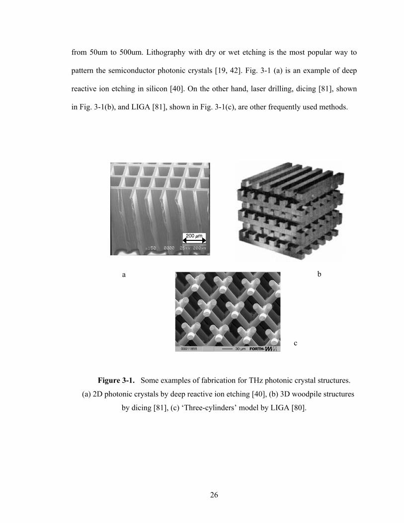
from 50um to 500um. Lithography with dry or wet etching is the most popular way to
pattern the semiconductor photonic crystals [19, 42]. Fig. 3-1 (a) is an example of deep
reactive ion etching in silicon [40]. On the other hand, laser drilling, dicing [81], shown
in Fig. 3-1(b), and LIGA [81], shown in Fig. 3-1(c), are other frequently used methods.
Figure 3-1. Some examples of fabrication for THz photonic crystal structures.
(a) 2D photonic crystals by deep reactive ion etching [40], (b) 3D woodpile structures
by dicing [81], (c) ‘Three-cylinders’ model by LIGA [80].
c
b a
26
3.2 MEMS technology for polymer and metallic photonic crystal
structures
We employ Micro-Electro-Mechanical-Systems (MEMS) technology [82] to make
the high quality THz 2D photonic crystal structures. Uniform photonic crystal structures
with very smooth sidewalls are easily formed without undercutting by using the MEMS
approach [46].
Polymer photonic crystal structures
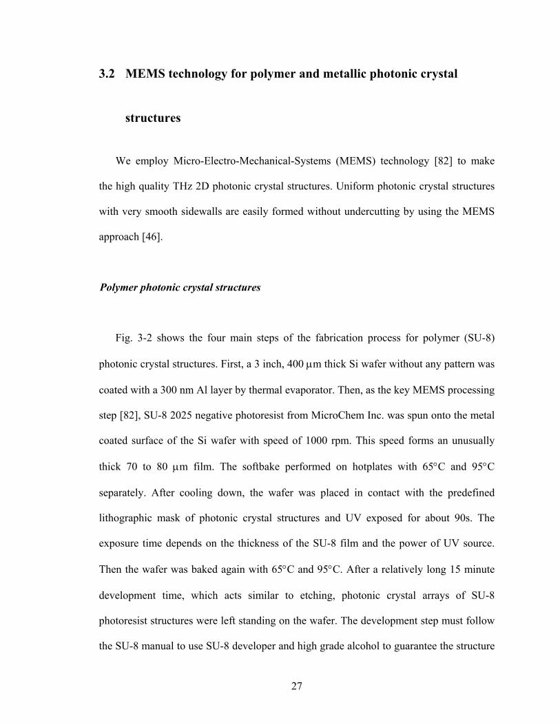
Fig. 3-2 shows the four main steps of the fabrication process for polymer (SU-8)
photonic crystal structures. First, a 3 inch, 400 µm thick Si wafer without any pattern was
coated with a 300 nm Al layer by thermal evaporator. Then, as the key MEMS processing
step [82], SU-8 2025 negative photoresist from MicroChem Inc. was spun onto the metal
coated surface of the Si wafer with speed of 1000 rpm. This speed forms an unusually
thick 70 to 80 µm film. The softbake performed on hotplates with 65°C and 95°C
separately. After cooling down, the wafer was placed in contact with the predefined
lithographic mask of photonic crystal structures and UV exposed for about 90s. The
exposure time depends on the thickness of the SU-8 film and the power of UV source.
Then the wafer was baked again with 65°C and 95°C. After a relatively long 15 minute
development time, which acts similar to etching, photonic crystal arrays of SU-8
photoresist structures were left standing on the wafer. The development step must follow
the SU-8 manual to use SU-8 developer and high grade alcohol to guarantee the structure
27
quality. A five minute higher temperature bake at 150o C changed the photoresist arrays
into arrays of hard polymer standing structures. Finally, the processed Si wafer was
diced into oriented 25 mm-wide by 10 mm-long chips to fit over the lower plate of the
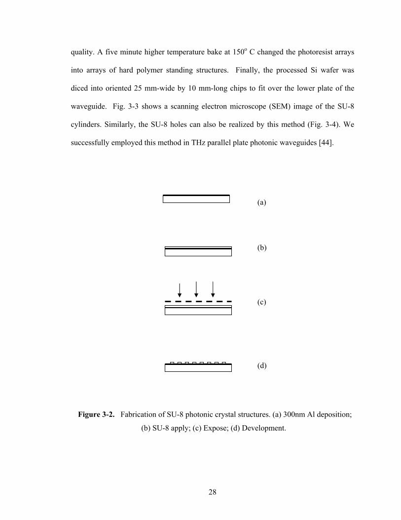
waveguide. Fig. 3-3 shows a scanning electron microscope (SEM) image of the SU-8
cylinders. Similarly, the SU-8 holes can also be realized by this method (Fig. 3-4). We
successfully employed this method in THz parallel plate photonic waveguides [44].
(a) (b) (c) (d)
Figure 3-2. Fabrication of SU-8 photonic crystal structures. (a) 300nm Al deposition;
(b) SU-8 apply; (c) Expose; (d) Development.
28
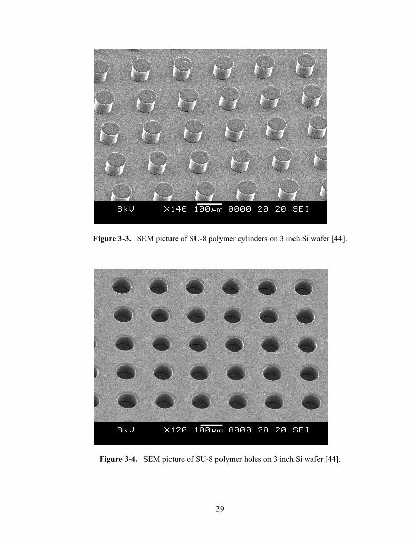
Figure 3-3. SEM picture of SU-8 polymer cylinders on 3 inch Si wafer [44].
Figure 3-4. SEM picture of SU-8 polymer holes on 3 inch Si wafer [44].
29
Metallic photonic crystal structures
The first part of process for metallic photonic crystal structure is the same as the SU-8
photonic crystal structures. After changing to the polymer by the long high temperature
baking, a thick layer of metal is coated on the sample surface to transform polymer
photonic crystals into metallic photonic crystals. The critical issue for photonic crystal
coating is to guarantee the film quality of structures’ sidewall. We employed two
methods to coat the samples, sputtering and glancing angle deposition.
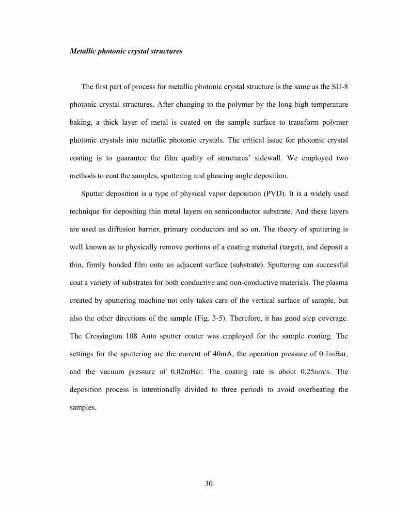
Sputter deposition is a type of physical vapor deposition (PVD). It is a widely used
technique for depositing thin metal layers on semiconductor substrate. And these layers
are used as diffusion barrier, primary conductors and so on. The theory of sputtering is
well known as to physically remove portions of a coating material (target), and deposit a
thin, firmly bonded film onto an adjacent surface (substrate). Sputtering can successful
coat a variety of substrates for both conductive and non-conductive materials. The plasma
created by sputtering machine not only takes care of the vertical surface of sample, but
also the other directions of the sample (Fig. 3-5). Therefore, it has good step coverage.
The Cressington 108 Auto sputter coater was employed for the sample coating. The
settings for the sputtering are the current of 40mA, the operation pressure of 0.1mBar,
and the vacuum pressure of 0.02mBar. The coating rate is about 0.25nm/s. The
deposition process is intentionally divided to three periods to avoid overheating the
samples.
30
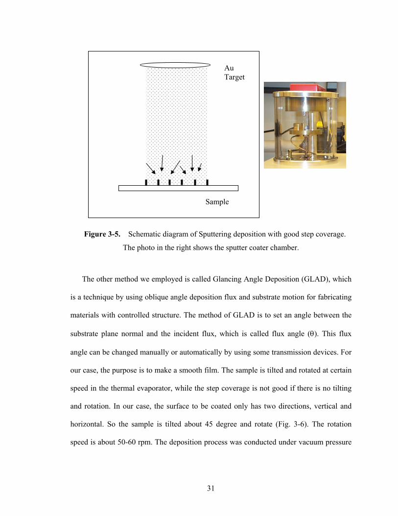
Au Target
Sample
Figure 3-5. Schematic diagram of Sputtering deposition with good step coverage.
The photo in the right shows the sputter coater chamber.
The other method we employed is called Glancing Angle Deposition (GLAD), which
is a technique by using oblique angle deposition flux and substrate motion for fabricating
materials with controlled structure. The method of GLAD is to set an angle between the
substrate plane normal and the incident flux, which is called flux angle (θ). This flux
angle can be changed manually or automatically by using some transmission devices. For
our case, the purpose is to make a smooth film. The sample is tilted and rotated at certain
speed in the thermal evaporator, while the step coverage is not good if there is no tilting
and rotation. In our case, the surface to be coated only has two directions, vertical and
horizontal. So the sample is tilted about 45 degree and rotate (Fig. 3-6). The rotation
speed is about 50-60 rpm. The deposition process was conducted under vacuum pressure
31
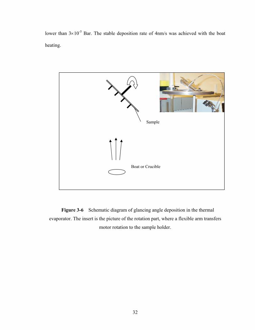
lower than 3×10⁻⁵ Bar. The stable deposition rate of 4nm/s was achieved with the boat
heating.
Boat or Crucible
Sample
Figure 3-6 Schematic diagram of glancing angle deposition in the thermal
evaporator. The insert is the picture of the rotation part, where a flexible arm transfers
motor rotation to the sample holder.
32
3.3 Dicing for semiconductor photonic crystal structures
Micromachining is powerful tool to fabricate the 1D, 2D and 3D photonic crystal
structures. It includes dicing, drilling and molding. The dicing machine for
semiconductor chip has a resolution better than 1µm, which makes it easy to realize the
THz photonic crystal structures. R. Gonzalo et. al. have demonstrated this method to
fabricate 3D layer by layer or woodpile photonic crystal structures in submillimeter
frequencies [81].
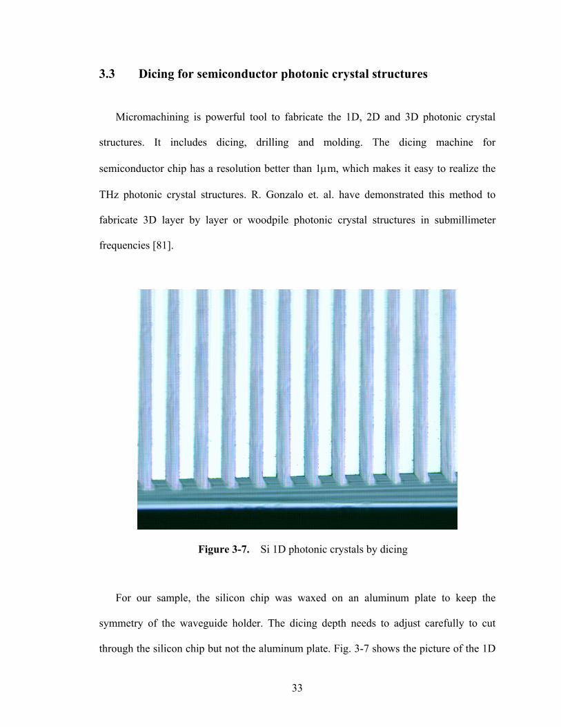
Figure 3-7. Si 1D photonic crystals by dicing
For our sample, the silicon chip was waxed on an aluminum plate to keep the
symmetry of the waveguide holder. The dicing depth needs to adjust carefully to cut
through the silicon chip but not the aluminum plate. Fig. 3-7 shows the picture of the 1D
33
photonic crystal sample. The blades used in dicing machine have different types. There
are hubless or hub blade with various thickness. According to the periodicity of the
structures, different type of blade should be selected. Usually, the resulted width of cuts
is broader than the thickness of the blade because of kerf loss.
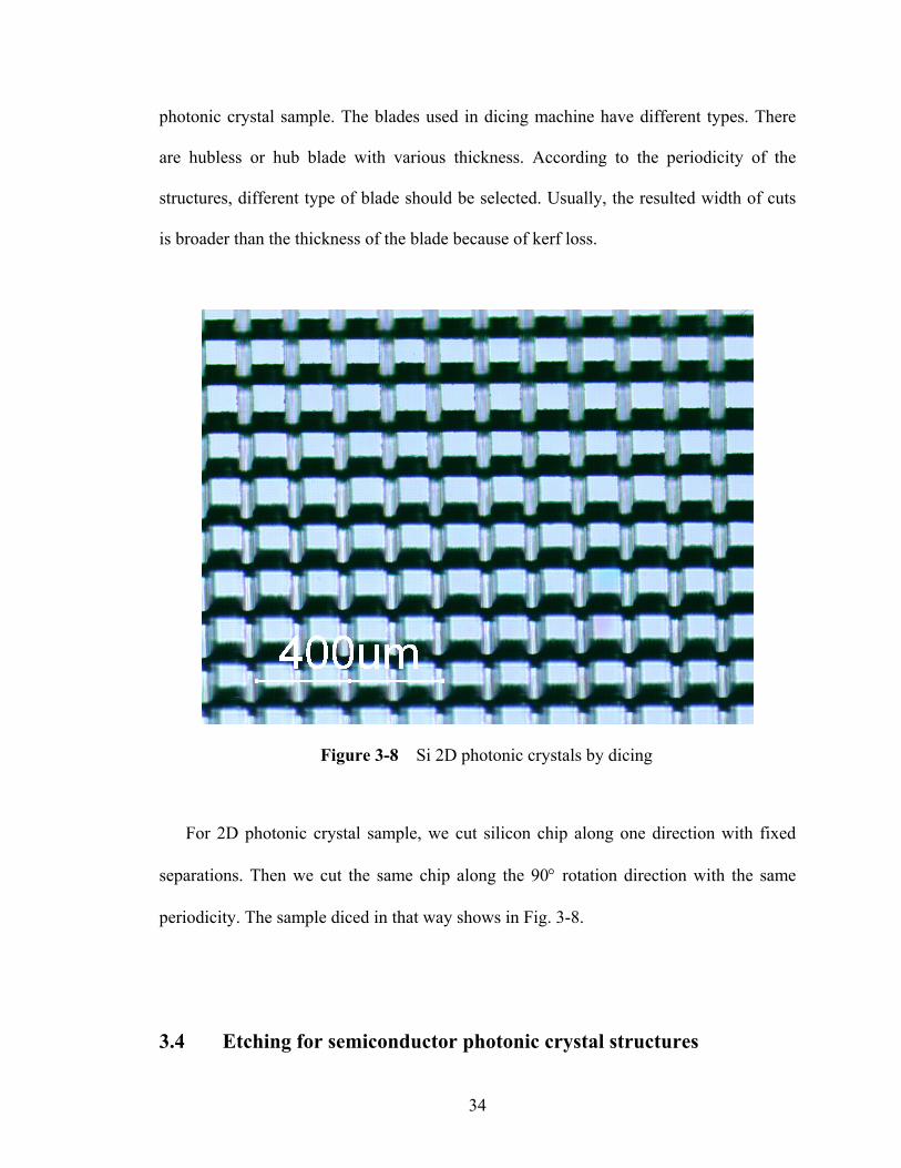
Figure 3-8 Si 2D photonic crystals by dicing
For 2D photonic crystal sample, we cut silicon chip along one direction with fixed
separations. Then we cut the same chip along the 90° rotation direction with the same
periodicity. The sample diced in that way shows in Fig. 3-8.
3.4 Etching for semiconductor photonic crystal structures
34
Here, we just briefly mention this method because we don’t have high quality deep
reaction ion etching machine (DRIE). The reaction ion etching machine (RIE) can etch a
thick silicon chip but has severe undercutting. We use SU-8 negative photoresist as the
etching mask to protect the unetched parts. For RIE operation, the gas applied in the
chamber combined SF6 and O2 with 80% and 20% ratio (SF6 is 12.5sccm and O2 is
1.5sccm). RF power is at 400W. The base pressure is set to 60mTorr. The etching rate is
about 5um/min.
Figure 3-9 Si 2D photonic crystals by etching
In a 50um thick silicon piece, we formed the periodic structure shown on Fig. 3-9.
We can clearly see the SU-8 mask and undercutting in the figure. Although the structure
is not perfect, this kind of structure can create band gap. However, the simulation may be
35
a little bit difficult. By this method, some other experiments such as THz surface-plasma
polaritons can also be done and extraordinary transmission from this structure was
observed [83].
36
CHAPTER IV
EXPERIMENTAL SETUP
4.1 The samples design
First, the samples are sandwiched between two metal plates. We need to take
advantage of the single TEM mode and good coupling properties of parallel plate
waveguide. Second, we also need to consider about the delay of reflection from the edge
of photonic crystal structures to ensure the complete signal sampling. So the sample
design must have enough distance from the silicon lens to the edge of the photonic crystal
structures. Fig. 4-1 shows one of the samples. The patterns on the top and bottom are
functional as spacers which give enough mechanical support for the sample patterns in
the center.
The design of photonic crystal structures depends on three parameters: the dielectric
constants of two materials (such as air and polymer in our case); the filling ratio, or the
radius and lattice constant ratio; and the lattice pattern of the samples (such as triangular,
square). The development of computation technology provides an easy way to simulate
the results before fabrication.
37
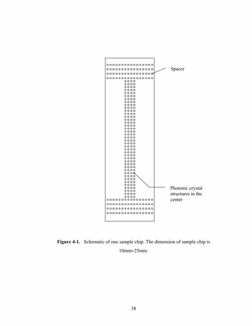
Spacer
Photonic crystal structures in the center
Figure 4-1. Schematic of one sample chip. The dimension of sample chip is
10mm×25mm.
38
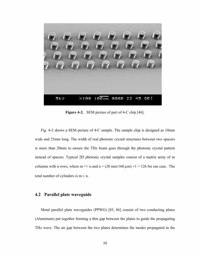
Figure 4-2. SEM picture of part of 4-C chip [46].
Fig. 4-2 shows a SEM picture of 4-C sample. The sample chip is designed as 10mm
wide and 25mm long. The width of real photonic crystal structures between two spacers
is more than 20mm to ensure the THz beam goes through the photonic crystal pattern
instead of spacers. Typical 2D photonic crystal samples consist of a matrix array of m
columns with n rows, where m << n and n = (20 mm/160 µm) +1 = 126 for our case. The
total number of cylinders is m × n.
4.2 Parallel plate waveguide
Metal parallel plate waveguides (PPWG) [85, 86] consist of two conducting plates
(Aluminum) put together forming a thin gap between the plates to guide the propagating
THz wave. The air gap between the two plates determines the modes propagated in the
39
waveguide. The cutoff frequency is defined by bnmcfc 2= , where m is mode number, b
is the gap of two plates, and n is the refractive index of material between two plates. With
a 70 µm gap, the cutoff frequency of TM1 is 2.1 THz. But the odd TM1 mode does not
couple into PPWG. The cutoff frequency of TM2 is 4.2 THz, which means that only the
TEM mode existed below 4.2 THz. The concepts and utility of the single TEM mode
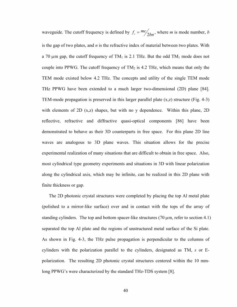
THz PPWG have been extended to a much larger two-dimensional (2D) plane [84].
TEM-mode propagation is preserved in this larger parallel plate (x,z) structure (Fig. 4-3)
with elements of 2D (x,z) shapes, but with no y dependence. Within this plane, 2D
reflective, refractive and diffractive quasi-optical components [86] have been
demonstrated to behave as their 3D counterparts in free space. For this plane 2D line
waves are analogous to 3D plane waves. This situation allows for the precise
experimental realization of many situations that are difficult to obtain in free space. Also,
most cylindrical type geometry experiments and situations in 3D with linear polarization
along the cylindrical axis, which may be infinite, can be realized in this 2D plane with
finite thickness or gap.
The 2D photonic crystal structures were completed by placing the top Al metal plate
(polished to a mirror-like surface) over and in contact with the tops of the array of
standing cylinders. The top and bottom spacer-like structures (70 µm, refer to section 4.1)
separated the top Al plate and the regions of unstructured metal surface of the Si plate.
As shown in Fig. 4-3, the THz pulse propagation is perpendicular to the columns of
cylinders with the polarization parallel to the cylinders, designated as TM, s or E-
polarization. The resulting 2D photonic crystal structures centered within the 10 mm-
long PPWG’s were characterized by the standard THz-TDS system [8].
40
Figure 4-3. The not-to-scale sideview and 3D view of the setup of the sample in the
waveguide with the wave coupling by two silicon lenses [77].
THz
Top Metal plate
THz Pulse E
Input Coupling Lens
Sample chip
y n-column sample
x z
41
4.3 Setup in THz-TDS
The THz optical arrangement converts the incident 3D plane wave from the THz
transmitter into an incident 2D line wave matched to the waveguide and couples the
waveguide output 2D line wave into an outgoing 3D plane wave which is then efficiently
coupled into the THz receiver [85]. Two plano-cylindrical high-resistivity silicon lenses
(Figure 4-3) are used to couple the radiation into and out of the reference or sample
waveguide, placed at the confocal beam waist of the THz-TDS system (Fig. 4-4). The
lenses are 15 mm x 10 mm x 6.56 mm with a 5 mm radius of curvature. The input lens
focuses the incoming THz radiation to an elliptical spot with a frequency independent
minor axis of 150 µm, perpendicular to the waveguide plates, and a linearly wavelength-
dependent major axis parallel to the plates with a 1/e amplitude diameter d = 9 mm at 1
THz. Within the PPWG this situation gives a frequency independent 2D THz beam
divergence θ ≅ λ/d = 0.3/9 = 0.033 rad, which is also the angular acceptance of the THz
receiver. This narrow acceptance angle of the THz receiver is important for our
measurements, because the forward (zero order) transmission through the photonic
crystal structures is expected to be sharply angular dependent, which is similar to a
transmission grating, requiring good angular resolution to obtain the proper on-axis signal
strength.
The pump and probe laser pulse beams are created by a KLM Ti:Sapphire laser which
is pumped by a Spectral Physics Millennia cw laser. The laser beam has 40fs pulse train
with a nominal wavelength of 820nm and a repetition rate of 100MHz. The average
powers of pump and probe laser beam are adjusted to about 10mW. The transmitter is
biased with 70V DC and the receiver has a very highly sensitive current amplifier. A
42
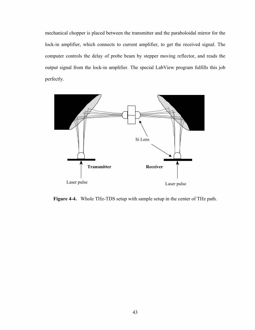
mechanical chopper is placed between the transmitter and the paraboloidal mirror for the
lock-in amplifier, which connects to current amplifier, to get the received signal. The
computer controls the delay of probe beam by stepper moving reflector, and reads the
output signal from the lock-in amplifier. The special LabView program fulfills this job
perfectly.
Laser pulse Laser pulse
Si Lens
Receiver
Transmitter
Figure 4-4. Whole THz-TDS setup with sample setup in the center of THz path.
43
CHAPTER V
STUDY OF BASIC THz PHOTONIC CRYSTALS
5.1 Polymer (SU-8) photonic crystal structures
Dielectric photonic crystals are the major subjects for science research in meta-
materials [3]. The first investigation of THz photonic crystals was based on dielectric
materials [19]. In order to understand the behavior of photonic crystals in PPWG, it is
necessary to conduct the dielectric (polymer) research on this setup [46]. The 2D polymer
sample fabrication followed the method of section 3.2. The photonic crystal structures
consist of a square array of cylinders in air with lattice constants of 160µm, diameters of
65µm and heights of 70µm. Four samples with zero-column (blank), 4-column (4-C), 8-
column (8-C) and 60 column (60-C) arrays of cylinders were separately fabricated for the
polymer (SU-8) photonic crystal experiment.
Fig. 5-1 shows the transmitted THz reference pulse together with three different
sample pulses, which have propagated through the 4-C, 8-C, or 60-C, 2D photonic crystal
structures, respectively. The baselines of the three sample pulses in Fig. 5-1(a) have been
offset for clarity. The THz reference pulse was transmitted without distortion through the
44
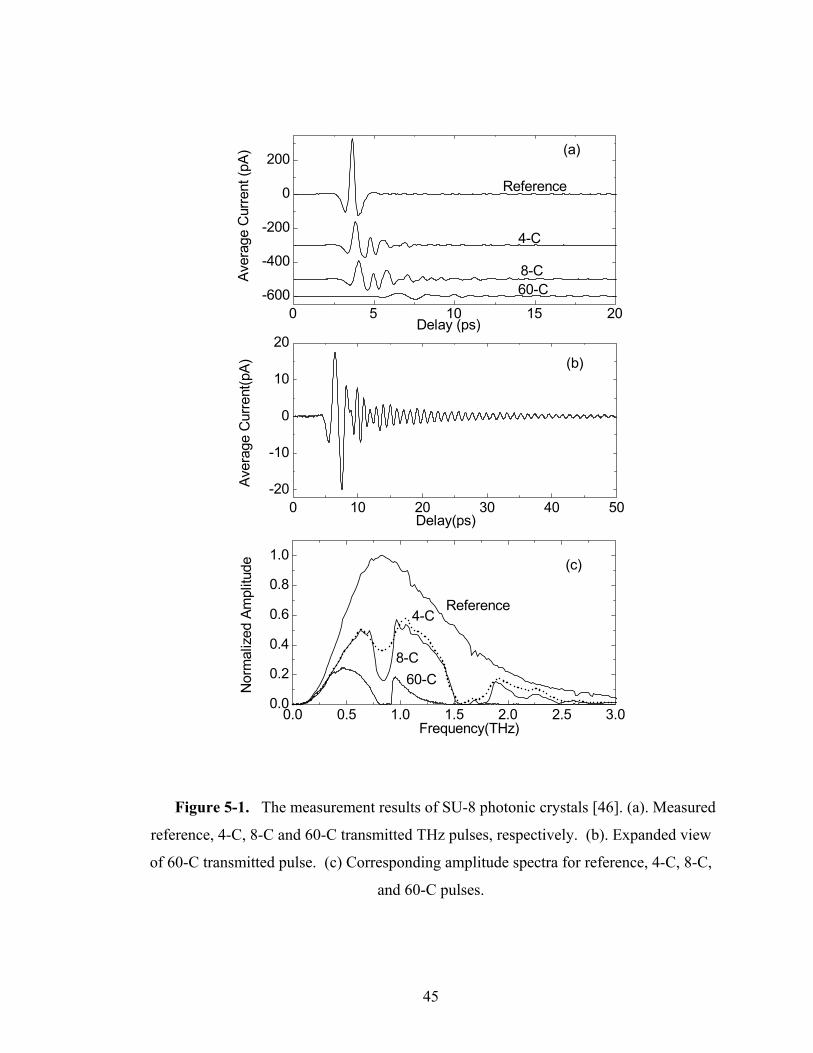
0 5 10 15 20-600
-400
-200
0
200
0 10 20 30 40 50-20
-10
0
10
20
0.0 0.5 1.0 1.5 2.0 2.5 3.00.0
0.2
0.4
0.6
0.8
1.0
(a)
60-C8-C
4-C
Reference
Aver
age
Cur
rent
(pA)
Delay (ps)
(b)
Aver
age
Cur
rent
(pA)
Delay(ps)
60-C8-C
4-CReference
(c)
Nor
mal
ized
Am
plitu
de
Frequency(THz)
Figure 5-1. The measurement results of SU-8 photonic crystals [46]. (a). Measured
reference, 4-C, 8-C and 60-C transmitted THz pulses, respectively. (b). Expanded view
of 60-C transmitted pulse. (c) Corresponding amplitude spectra for reference, 4-C, 8-C,
and 60-C pulses.
45
25 mm wide by 10 mm long PPWG with 70 µm plate separation and no photonic crystal
structure in place (blank sample). Compared to the reference pulse, the sample pulses
were attenuated, reshaped, and developed a low-level ringing structure extending to
approximately 20 ps for the 4-C and 8-C pulses, and to 100 ps for the 60-C pulse. In
addition, the leading edges of the sample pulses show slight propagation delays with
respect to the reference pulse, which propagates at the free-space speed of light c. These
delays of 0.2 ps for 4-C, 0.4 ps for 8-C and 2.9 ps for 60-C structures are in approximate
agreement with those calculated from a simple filling factor argument. The filling factor
F is given by the ratio of the cross-sectional area of a cylinder to the lattice spacing area.
130.0)160/()2/65( 22 =×= mmF µµπ (38)
The calculated delay D is then given by
cnFmND /)1()160( −×××= µ (39)
Where N is the number of columns, n = 1.7 is the refractive index of the SU-8
cylinders, and c is the speed of light. The calculated values from the above equation are D
= 0.19, 0.39 and 2.91 ps for N = 4, 8 and 60, respectively.
Fig. 5-1(b) shows more detail of the 60-C pulse. It presents the complex reshaped
waveform with a ringing monotonic decay, measured with a signal-to-noise ratio (SNR)
of approximately 300. Fig. 5-1(c) shows the corresponding amplitude spectra of the
reference pulse and the three sample pulses, demonstrating the filtering capability of the
4-C, 8-C and 60-C structures. Well resolved spectral features are observed, which
increase in strength from the 4-C compared to the 8-C compared to the 60-C structure.
The amplitudes of the spectral peaks have been reduced by the dielectric absorption of
46
the cylinders. In order to have the highest frequency resolution, the 60-C spectrum is the
transform of the complete 60-C pulse extending to 100 ps.
Fig. 5-2 (a) shows the amplitude transmission for all three samples. Here, the arising
of the band gap feature strength with the number of columns is clearly demonstrated.
The 60-C spectrum shows a well-defined band gap from 0.81 to 0.91 THz with a very
sharp (0.01 THz) turn-on at 0.91 THz. The 8-C transmission shows the same band gap in
a developing stage and another developing band gap at a higher frequency range from 1.5
to 1.84 THz, which contains a small relatively sharp transmission peak at 1.70 THz. One
discrepancy is that the measured transmission from low frequencies to the edge of the
first band gap at 0.8 THz is significantly lower than theoretical predictions for a plane
wave propagating through a similar 3D array of endless columns of infinitely long
cylinders. A possible reason for this reduction is that the finite extent of our 2D beam
reduces the on axis (zero-order) transmission by broadening the angular divergence. Fig.
5-2 (b) presents the relative phase of the sample pulses with respect to the reference pulse.
The dashed lines associated with each sample pulse are the phase shifts Φ determined by
the filling factor time delay.
)1()/160(2 −×××=Φ nFmN λµπ (40)
The observable features deviating from the dashed lines describe the phase response
associated with 2D band gap features in the transmission of Fig. 5-2(a). The large
absorption of the 60-C sample truncated the phase determination below 1 THz.
47
0 0.5 1 1.5 2 2.5 30
0.1
0.2
0.3
0.4
0.5
0.6
0.7
0.8
Frequency (THz)
Ampl
itude
Tra
nsm
issi
on
60-C
8-C
4-C
8-C
4-C (a)
0 0.5 1 1.5 2 2.5 3-20
-15
-10
-5
0
Frequency (THz)
Pha
se A
ngle
(rad
)
4-C
8-C
60-C
(b)
Figure 5-2. (a). Amplitude transmission of the 4-C, 8-C and 60-C samples, respectively.
(b). Calculated phase shift (dashed curves) and measured relative phase shift (solid
curves) for 4-C, 8-C, and 60-C pulses [46].
48
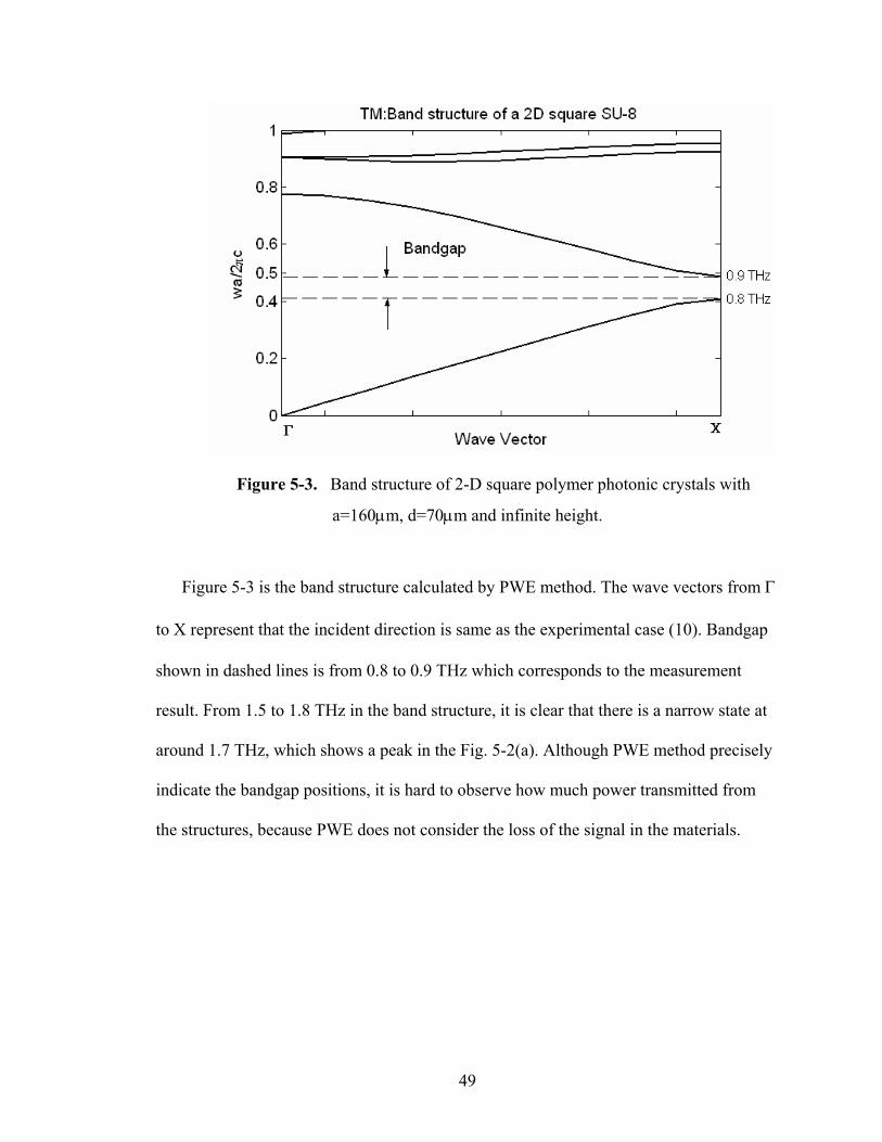
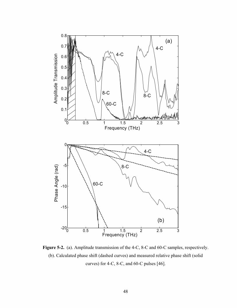
Figure 5-3. Band structure of 2-D square polymer photonic crystals with
a=160µm, d=70µm and infinite height.
Figure 5-3 is the band structure calculated by PWE method. The wave vectors from Γ
to Χ represent that the incident direction is same as the experimental case (10). Bandgap
shown in dashed lines is from 0.8 to 0.9 THz which corresponds to the measurement
result. From 1.5 to 1.8 THz in the band structure, it is clear that there is a narrow state at
around 1.7 THz, which shows a peak in the Fig. 5-2(a). Although PWE method precisely
indicate the bandgap positions, it is hard to observe how much power transmitted from
the structures, because PWE does not consider the loss of the signal in the materials.
49
0 0.5 1 1.5 2 2.5 3-60
-50
-40
-30
-20
-10
0
Frequency (THz)
Pow
er T
rans
mis
sion
(dB
) 4-C
60-C
Figure 5-4. Measured power transmission for the 4-C and 60-C samples (solid curves)
compared with theory (dotted curves).
Fig. 5-4 shows the power transmission measurements T(ω) in dB of the 4-C and 60-C
structures. The T(ω) calculated by
)()(log20)(
ωωω
RST = (41)
Where S(ω) is the sample amplitude spectrum and R(ω) is the reference spectrum.
Here, we compare our experimental results with numerical TMM calculations [65].
For our case the ratio of cylinder radius to the square lattice constant is (32.5 µm)/(160
µm) = 0.203; based on our THz-TDS measurements of cured SU-8 2025 photoresist and
previous THz-TDS measurements [87], the real part of the frequency-dependent index of
50
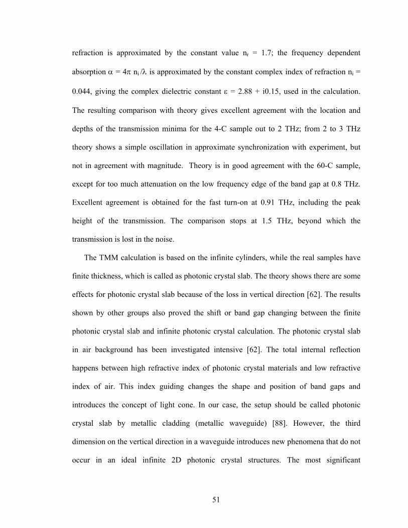
refraction is approximated by the constant value nr = 1.7; the frequency dependent
absorption α = 4π ni /λ is approximated by the constant complex index of refraction ni =
0.044, giving the complex dielectric constant ε = 2.88 + i0.15, used in the calculation.
The resulting comparison with theory gives excellent agreement with the location and
depths of the transmission minima for the 4-C sample out to 2 THz; from 2 to 3 THz
theory shows a simple oscillation in approximate synchronization with experiment, but
not in agreement with magnitude. Theory is in good agreement with the 60-C sample,
except for too much attenuation on the low frequency edge of the band gap at 0.8 THz.
Excellent agreement is obtained for the fast turn-on at 0.91 THz, including the peak
height of the transmission. The comparison stops at 1.5 THz, beyond which the
transmission is lost in the noise.
The TMM calculation is based on the infinite cylinders, while the real samples have
finite thickness, which is called as photonic crystal slab. The theory shows there are some
effects for photonic crystal slab because of the loss in vertical direction [62]. The results
shown by other groups also proved the shift or band gap changing between the finite
photonic crystal slab and infinite photonic crystal calculation. The photonic crystal slab
in air background has been investigated intensive [62]. The total internal reflection
happens between high refractive index of photonic crystal materials and low refractive
index of air. This index guiding changes the shape and position of band gaps and
introduces the concept of light cone. In our case, the setup should be called photonic
crystal slab by metallic cladding (metallic waveguide) [88]. However, the third
dimension on the vertical direction in a waveguide introduces new phenomena that do not
occur in an ideal infinite 2D photonic crystal structures. The most significant
51
confinement effect is the mixing of modes with different polarizations, TE or TM
polarized in 2D structures. The mixing modifies the band structure, causing anticrossings
where modes of opposite polarization intersect. The mixing can also lead to polarization
conversion if symmetry allows. This kind of polarization conversion was observed in
waveguide propagation measurements [89].
The advantage of our experimental setup is that there is only a single TEM mode
existing in the waveguide. The mixing of TE and TM polarization does not happen. The
way of using 2D structures to simulate 3D structures with infinite thickness are realized
and proved by our setup and experiment. In the experiments, the single mode is
conserved below 4 THz as calculated in section 4.2. The simulation result matches the
experimental result well without shift and band changing. However, we can see a little
band changing in 60-C sample, which may be contributed by the frequency dependent
index and absorption, as well as the reflection at the edge of the 60-C sample.
52
5.2 Metallic photonic crystal structures
Metallic photonic crystals (MPCs) have shown unique characteristics over the
dielectric photonic crystals, such as wider bandgap, lighter weight, smaller size [4]. The
method to fabricate high quality pure metallic photonic crystals needs precise mechanical
machines. Instead of that, the metal coating method is easier to design and fabricate. The
metal coating photonic crystal structures also show the same properties as the pure
metallic photonic crystals.
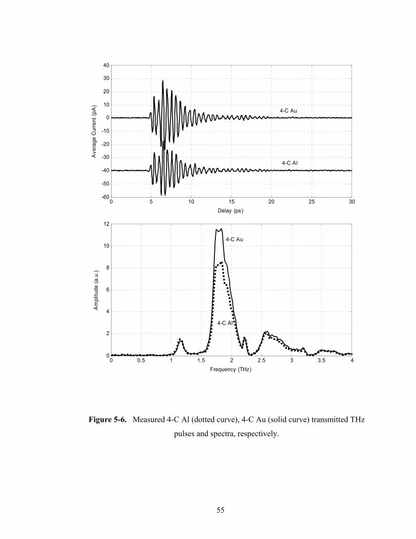
Two samples are tested in the THz-TDS system using parallel plate waveguide to
guide THz in and out from the photonic crystal structures. These two samples, with Al
and Au coating, have the same structures consisting of 4 columns cylinders. The
periodicity is 160µm, the diameter of the cylinders is 70µm and the height of the
cylinders is 70µm. The experiment process is the same as that in the section 5.1.
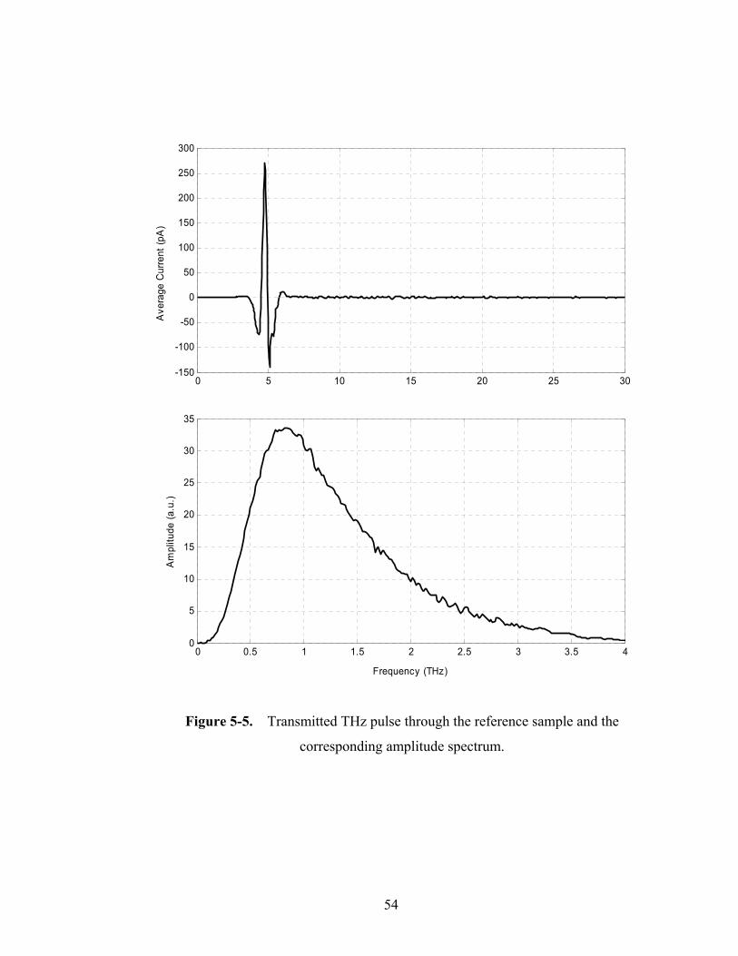
Fig. 5-5 shows the reference pulse and spectrum. Fig. 5-6 shows 4-C Al sample and
4-C Au sample pulses and spectra. The pulses from the samples have ringing structure
extended to 30 ps. The propagation delay of both sample pulses is about 0.2 ps with
respect to the reference pulse. From the spectra, it is clear that the bandgaps are from low
frequency around 0 to 1.1 THz and from 1.2 to 1.65 THz. We noticed that the positions
of bandgaps are almost same, because Au and Al samples have similar dimensions. The
amplitude of Au is a little higher than that of Al samples due to the difference of
conductivity, which relates to the loss on metal surface.
53
0 5 10 15 20 25 30-150
-100
-50
0
50
100
150
200
250
300
Delay (ps)
Ave
rage
Cur
rent
(pA
)
0 0.5 1 1.5 2 2.5 3 3.5 40
5
10
15
20
25
30
35
Frequency (THz)
Am
plitu
de (a
.u.)
Figure 5-5. Transmitted THz pulse through the reference sample and the
corresponding amplitude spectrum.
54
0 5 10 15 20 25 30-60
-50
-40
-30
-20
-10
0
10
20
30
40
Delay (ps)
Ave
rage
Cur
rent
(pA
)
0 0.5 1 1.5 2 2.5 3 3.5 40
2
4
6
8
10
12
Frequency (THz)
Am
plitu
de (a
.u.)
4-C Au
4-C Al
4-C Au
4-C Al
Figure 5-6. Measured 4-C Al (dotted curve), 4-C Au (solid curve) transmitted THz
pulses and spectra, respectively.
55
0 0.5 1 1.5 2 2.5 3 3.5 4-80
-70
-60
-50
-40
-30
-20
-10
0
Frequency (THz)
Tran
smis
sion
(dB
)
Au: 4-C wp=2175THzwt=6.5THz r/a=0.22
Calculation
Measurement
Figure 5-7. Measured power transmission for the 4-C Au sample (solid curve)
compared with theory (dotted curve).
At THz frequencies, within the approximations of the simple Drude model, the real
part of the dielectric constant of metal is a negative constant, while the much larger
imaginary part is to a good first order approximation proportional to the wavelength [9].
This information is needed for the theoretical modeling. The simple Drude model [90]
treats the free carriers in a metal as classical point charges subject to random collisions,
for which the collision damping is independent of the carrier velocity. According to the
model, the frequency-dependent complex dielectric constant εc (the square of the
complex index of refraction nc = n + ini) is given in SI units as
56
)(/)/( 20 τωωωωεωεσεε ii pc +−=+= ∞∞ (42)
where the corresponding Drude complex conductivity is given by
)/()/( 20 τττ ωωωεωωωσσ iiii pdc +=+= (43)
For the above relationships, ε∞ is the contribution of the bound electrons, ωτ = 1/τ is
the damping rate, and τ is the average collision time. The plasma angular frequency ωp is
defined by ωp2 = Ne2/(ε0m), where N is the number density of carriers, e is the electronic
charge, ε0 is the free-space permittivity, and m is the effective carrier mass. The dc
conductivity σdc is given by σdc = eµN with the mobility µ = e/(mωτ). The above
expression for εc can be rewritten in the form
)/1()( 00 ττ
τ
ωωωεσε
ωωωεωσεε
ii
idcdc
c −+=
+−= ∞∞
(44)
For the microwave and THz frequency ranges the ratio ω/ωτ << 1, and the above
expression for ε is, to a good first order approximation, given by
)/()/( 00 ωεσωεσεε τ dcdcc i+−≈ ∞ (45)
For the case of conducting metals ε can, to an excellent approximation, be further
reduced to
)/()/( 00 ωεσωεσε τ dcdcc i+−≈ (46)
In order to perform our numerical simulation, using the transfer matrix method
(TMM) [55, 65], we need two input parameters, the plasma frequency ωp and the
damping rate ωτ. These parameters are related to σdc by
20 pdc ωεωσ τ = (47)
Given the measurement of ωτ/2π = 6.5 THz for gold [79], and given the handbook Au
57
conductivity of σdc = 4.10×10⁷/(Ω⋅m) [91], ωp as calculated by the relationship ωp =
(σdcωτ/ε0)1/2, is equal to ωp / 2π = 2,175 THz. For Al, ωp = 3570 THz, ωτ = 19.4 THz.
Fig. 5-7 compares the experimental power transmission of the 4-C Au coating sample
and the calculated power transmission of the 4-C pure Au sample. The results fit very
well beyond 0.8 THz. Below 0.8 THz, there are some difference between the
experimental result and the calculated result because of the finite thickness of metal film.
The wave can penetrate the thin film when the skin depth is greater than the thickness of
the thin metal film, where the skin depth is inversely proportional to the square root of
frequency. If we take -30dB as the threshold, the band gaps are from 0.15 to 1.1 THz and
1.22 to 1.57 THz for experimental result. And the band gaps are from 0 to 1.03 THz and
1.22 to 1.55 THz for calculated result. The positions of the dips and peaks of
measurement results are identical with the calculated results. The amplitude deference is
believed to be caused by the alignment, fabrication and the loss of the samples.
Fig. 5-8 compares the experimental power transmission of the 4-C Al coating sample
and the calculated power transmission of the 4-C pure Al sample. The results fit well
beyond 0.85 THz. Below 0.85 THz, there are some difference between the experimental
result and the calculated result for the same reason as the Au sample. We still take -30dB
as the threshold. The first two band gaps are from 0.31 to 1.09 THz and from 1.34 to 1.6
THz for experimental result. And the first two band gaps are from 0 to 1.06 THz and
from 1.23 to 1.59 THz for the calculated result.
58
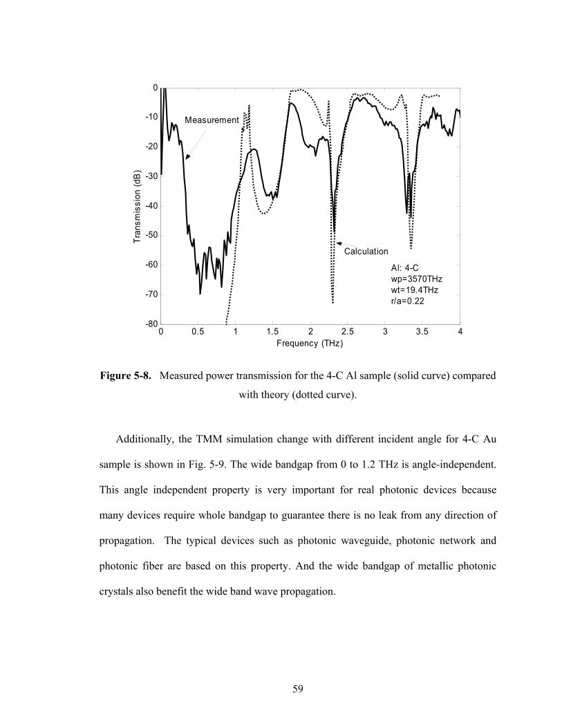
0 0.5 1 1.5 2 2.5 3 3.5 4-80
-70
-60
-50
-40
-30
-20
-10
0
Frequency (THz)
Tran
smis
sion
(dB
)
Al: 4-C wp=3570THzwt=19.4THzr/a=0.22
Calculation
Measurement
Figure 5-8. Measured power transmission for the 4-C Al sample (solid curve) compared
with theory (dotted curve).
Additionally, the TMM simulation change with different incident angle for 4-C Au
sample is shown in Fig. 5-9. The wide bandgap from 0 to 1.2 THz is angle-independent.
This angle independent property is very important for real photonic devices because
many devices require whole bandgap to guarantee there is no leak from any direction of
propagation. The typical devices such as photonic waveguide, photonic network and
photonic fiber are based on this property. And the wide bandgap of metallic photonic
crystals also benefit the wide band wave propagation.
59
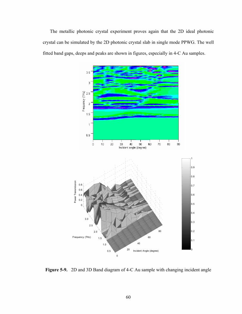
The metallic photonic crystal experiment proves again that the 2D ideal photonic
crystal can be simulated by the 2D photonic crystal slab in single mode PPWG. The well
fitted band gaps, deeps and peaks are shown in figures, especially in 4-C Au samples.
0
0.1
0.2
0.3
0.4
0.5
0.6
0.7
0.8
0.9
1
0
20
40
60
80
0.5
1.0
1.5
2.0
2.5
3.0
0
0.2
0.4
0.6
0.8
Incident Angle (degree)
Frequency (THz)
Pow
er T
rans
mis
sion
Figure 5-9. 2D and 3D Band diagram of 4-C Au sample with changing incident angle
60
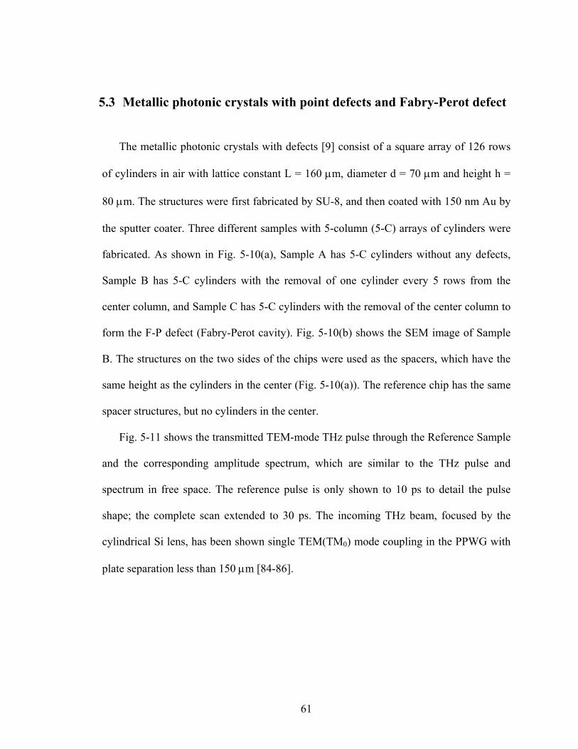
5.3 Metallic photonic crystals with point defects and Fabry-Perot defect
The metallic photonic crystals with defects [9] consist of a square array of 126 rows
of cylinders in air with lattice constant L = 160 µm, diameter d = 70 µm and height h =
80 µm. The structures were first fabricated by SU-8, and then coated with 150 nm Au by
the sputter coater. Three different samples with 5-column (5-C) arrays of cylinders were
fabricated. As shown in Fig. 5-10(a), Sample A has 5-C cylinders without any defects,
Sample B has 5-C cylinders with the removal of one cylinder every 5 rows from the
center column, and Sample C has 5-C cylinders with the removal of the center column to
form the F-P defect (Fabry-Perot cavity). Fig. 5-10(b) shows the SEM image of Sample
B. The structures on the two sides of the chips were used as the spacers, which have the
same height as the cylinders in the center (Fig. 5-10(a)). The reference chip has the same
spacer structures, but no cylinders in the center.
Fig. 5-11 shows the transmitted TEM-mode THz pulse through the Reference Sample
and the corresponding amplitude spectrum, which are similar to the THz pulse and
spectrum in free space. The reference pulse is only shown to 10 ps to detail the pulse
shape; the complete scan extended to 30 ps. The incoming THz beam, focused by the
cylindrical Si lens, has been shown single TEM(TM0) mode coupling in the PPWG with
plate separation less than 150 µm [84-86].
61
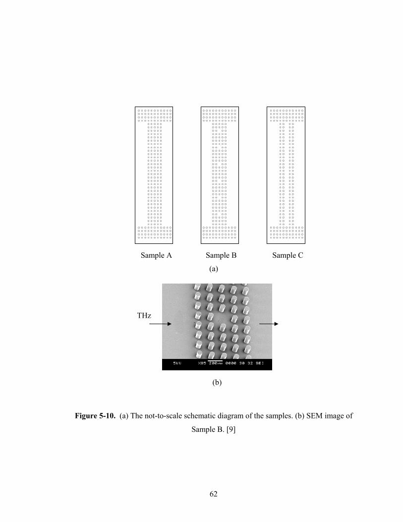
Figure 5-10. (a) The not-to-scale schematic diagram of the samples. (b) SEM image of
Sample B. [9]
(a)
(b)
Sample A Sample B Sample C
THz
62
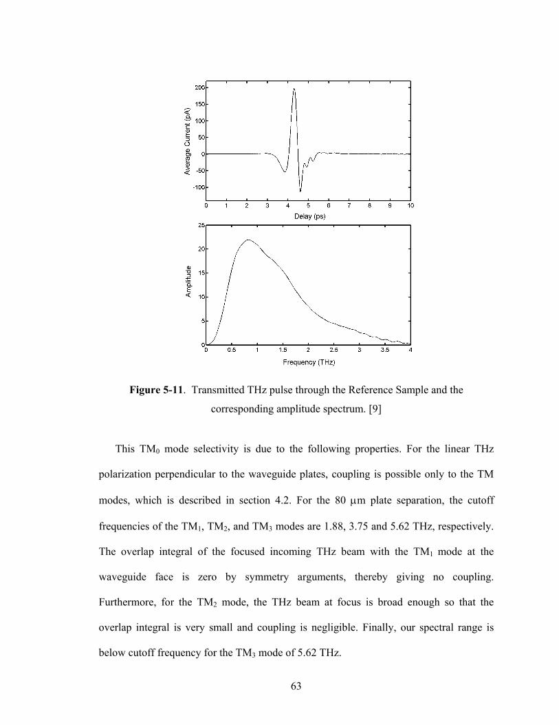
Figure 5-11. Transmitted THz pulse through the Reference Sample and the
corresponding amplitude spectrum. [9]
This TM0 mode selectivity is due to the following properties. For the linear THz
polarization perpendicular to the waveguide plates, coupling is possible only to the TM
modes, which is described in section 4.2. For the 80 µm plate separation, the cutoff
frequencies of the TM1, TM2, and TM3 modes are 1.88, 3.75 and 5.62 THz, respectively.
The overlap integral of the focused incoming THz beam with the TM1 mode at the
waveguide face is zero by symmetry arguments, thereby giving no coupling.
Furthermore, for the TM2 mode, the THz beam at focus is broad enough so that the
overlap integral is very small and coupling is negligible. Finally, our spectral range is
below cutoff frequency for the TM3 mode of 5.62 THz.
63
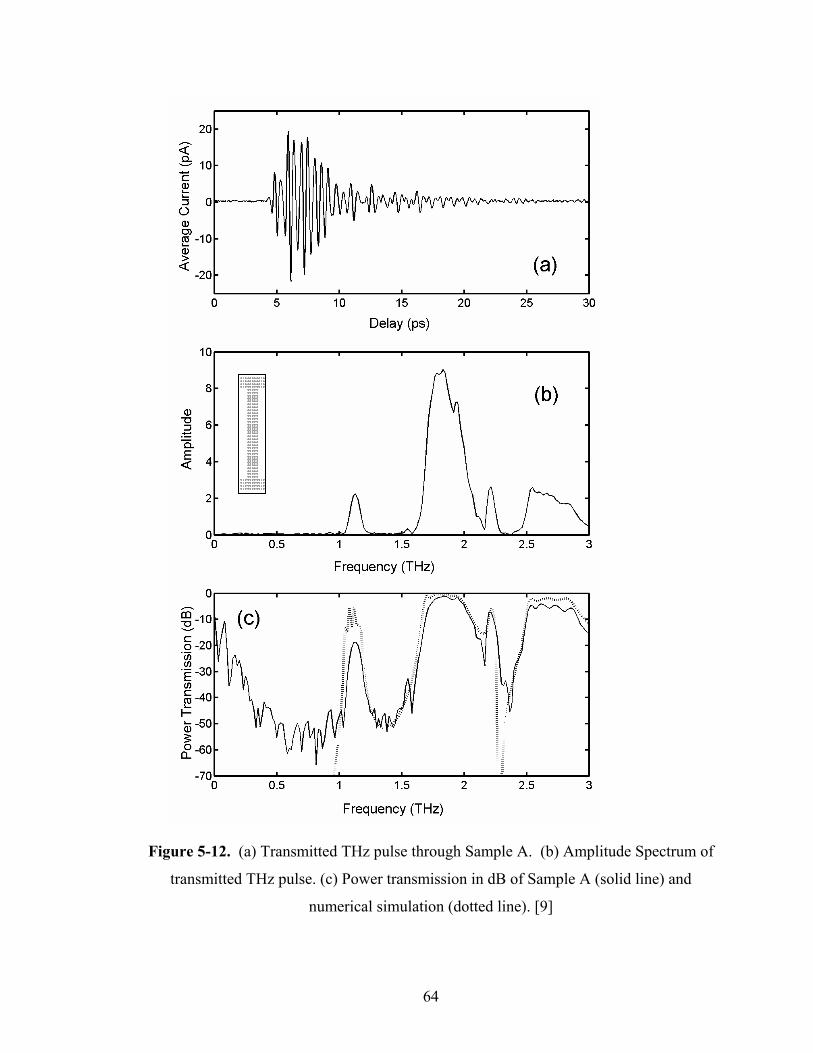
Figure 5-12. (a) Transmitted THz pulse through Sample A. (b) Amplitude Spectrum of
transmitted THz pulse. (c) Power transmission in dB of Sample A (solid line) and
numerical simulation (dotted line). [9]
64
Figures 5-12(a) and 5-12(b) show the transmitted THz pulse through Sample A and
the corresponding amplitude spectrum. The transmitted pulse from the sample has a
ringing structure extending to 25 ps. There is a small 0.2 ps propagation delay of the
sample pulse with respect to the reference pulse. From the spectrum, it is clear that the
first two bandgaps extend from low frequency to 1.0 THz and from 1.2 THz to 1.6 THz.
We simulated the results with TMM software [65]. The dielectric constant of metal is
frequency dependent and negative. It is difficult to apply this kind of dielectric constant
in to TMM. As sections 3.4 and 5.2 mentioned, the plasma frequency ωp and damping
frequency ωτ can be related to the dielectric constant. The metallic photonic crystal
simulation (TMM) employs these two parameters instead of the dielectric constant. For
Au, ωp= 2175 THz, ωτ = 6.5 THz.
Fig. 5-12(c) compares the measured power transmission of Sample A and the
simulated power transmission of a 5-C solid Au sample. Beyond 1 THz the results fit
very well. However, below 1 THz, there is significant difference considered to be due to
the finite thickness of the metal film. The THz waves can penetrate the 150 nm Au film
(leakage) when the skin depth is greater than the film thickness; the skin depth is
inversely proportional to the square root of frequency. For example, the skin depth of Au
is 102 nm at 0.5 THz. If we take -30 dB as the threshold, the measured band gaps are
from 0.22 to 1.07 THz and from 1.20 to 1.62 THz. In comparison, the calculated band
gaps are from 0 to 1.03 THz and from 1.19 to 1.60 THz. The corresponding positions of
the dips and peaks of the experimental results are in good agreement with the calculated
results.
65
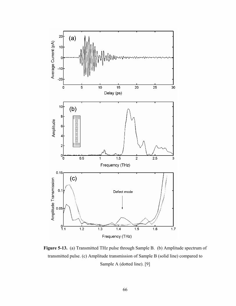
Figure 5-13. (a) Transmitted THz pulse through Sample B. (b) Amplitude spectrum of
transmitted pulse. (c) Amplitude transmission of Sample B (solid line) compared to
Sample A (dotted line). [9]
66
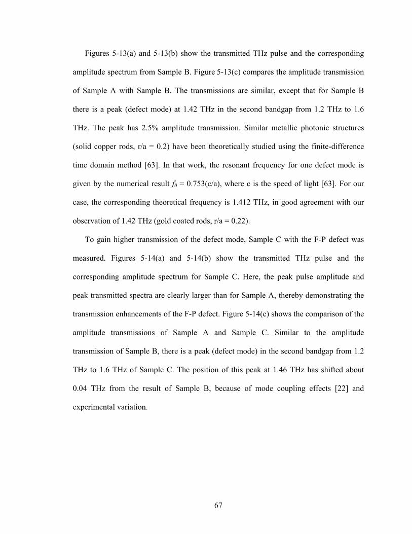
Figures 5-13(a) and 5-13(b) show the transmitted THz pulse and the corresponding
amplitude spectrum from Sample B. Figure 5-13(c) compares the amplitude transmission
of Sample A with Sample B. The transmissions are similar, except that for Sample B
there is a peak (defect mode) at 1.42 THz in the second bandgap from 1.2 THz to 1.6
THz. The peak has 2.5% amplitude transmission. Similar metallic photonic structures
(solid copper rods, r/a = 0.2) have been theoretically studied using the finite-difference
time domain method [63]. In that work, the resonant frequency for one defect mode is
given by the numerical result f0 = 0.753(c/a), where c is the speed of light [63]. For our
case, the corresponding theoretical frequency is 1.412 THz, in good agreement with our
observation of 1.42 THz (gold coated rods, r/a = 0.22).
To gain higher transmission of the defect mode, Sample C with the F-P defect was
measured. Figures 5-14(a) and 5-14(b) show the transmitted THz pulse and the
corresponding amplitude spectrum for Sample C. Here, the peak pulse amplitude and
peak transmitted spectra are clearly larger than for Sample A, thereby demonstrating the
transmission enhancements of the F-P defect. Figure 5-14(c) shows the comparison of the
amplitude transmissions of Sample A and Sample C. Similar to the amplitude
transmission of Sample B, there is a peak (defect mode) in the second bandgap from 1.2
THz to 1.6 THz of Sample C. The position of this peak at 1.46 THz has shifted about
0.04 THz from the result of Sample B, because of mode coupling effects [22] and
experimental variation.
67
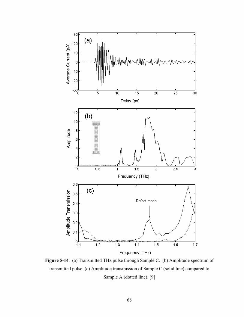
Figure 5-14. (a) Transmitted THz pulse through Sample C. (b) Amplitude spectrum of
transmitted pulse. (c) Amplitude transmission of Sample C (solid line) compared to
Sample A (dotted line). [9]
68
The peak with 22% amplitude transmission shows a very strong localization effect
compared with the point defect of Sample B. The defect mode frequency fr in the F-P
defect can be calculated by the F-P resonance condition )4()2( Lcmfr πφπ −= , where m
is the mode number, φ is the total phase contribution of two mirrors, and L is the
separation between the mirrors (L = 160 µm) [22]. For the defect mode at 1.46 THz, m is
evaluated as 2 and φ as 159 degrees.
For completeness, we compare these results with our unsuccessful attempt to create
and characterize 2D metallic photonic crystals in the PPWG by THz-TDS [44]. Initially,
we used a 2D photonic crystal of sputtered metal coated cylinders, 70 µm tall, 70 µm
diameter, and arranged on a 160 µm square lattice, lithographically fabricated on a
25.4mm-square Si plate. This 25.4 mm long structure filled the space between the plates
of the PPWG. However, due to the large number of metal coated columns (n=160), the
THz transmission through this structure was not observable. In order to obtain some
transmission, we broke the 2D symmetry by increasing the space between the waveguide
plates to let the tops of the metal coated cylinders form the surface of a 100 µm air gap to
the second plate. For this (theoretically undescribed) new class of air-spaced parallel
plate photonic waveguides, we observed strong photonic transmission effects, with stop
bands or transmission having contrasts of as much as 90 dB [44].
The measurements and characterizations of effectively 2D metallic photonic crystals
have been presented in the THz range. Wide bandgaps from 0 THz to 1.0 THz and from
1.1 THz to 1.6 THz were realized in the metallic photonic crystals, which fit well with
the simulation results. Strong localizations of the point defect mode and the F-P defect
were also observed. The convenient fabrication method and powerful metal PPWG setup
69
may enable applications, such as THz metallic photonic crystal cavities and photonic
networks.
The fact that these 2D photonic crystal structures were lithographically fabricated
using custom designed lithographic masks, demonstrates that any 2D photonic crystal
geometry consistent with the broad applicability of lithography can be achieved.
Furthermore, the fact that the theoretical simulations agree with experiment will allow for
accurate simulations of proposed structures, before mask design and fabrication.
Consequently, this work shows the possibility of design and fabrication of 2D photonic
crystals within the PPWG with specified frequency-dependent transmission.
70
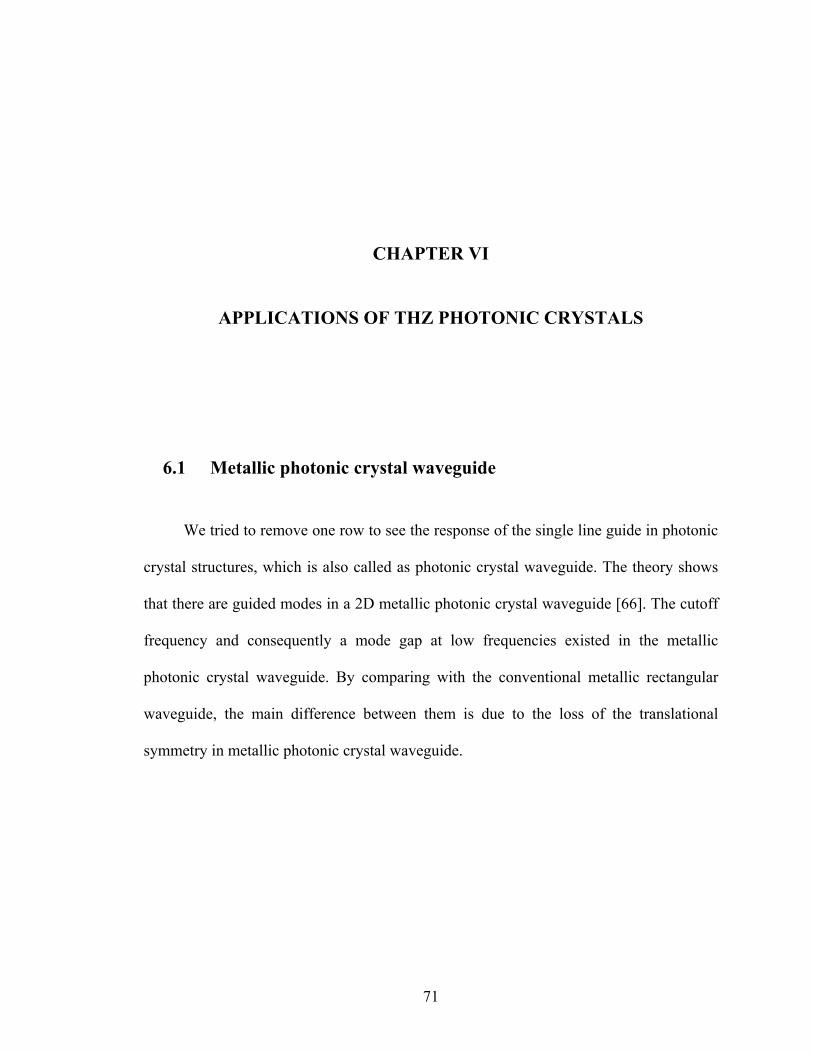
CHAPTER VI
APPLICATIONS OF THZ PHOTONIC CRYSTALS
6.1 Metallic photonic crystal waveguide
We tried to remove one row to see the response of the single line guide in photonic
crystal structures, which is also called as photonic crystal waveguide. The theory shows
that there are guided modes in a 2D metallic photonic crystal waveguide [66]. The cutoff
frequency and consequently a mode gap at low frequencies existed in the metallic
photonic crystal waveguide. By comparing with the conventional metallic rectangular
waveguide, the main difference between them is due to the loss of the translational
symmetry in metallic photonic crystal waveguide.
71
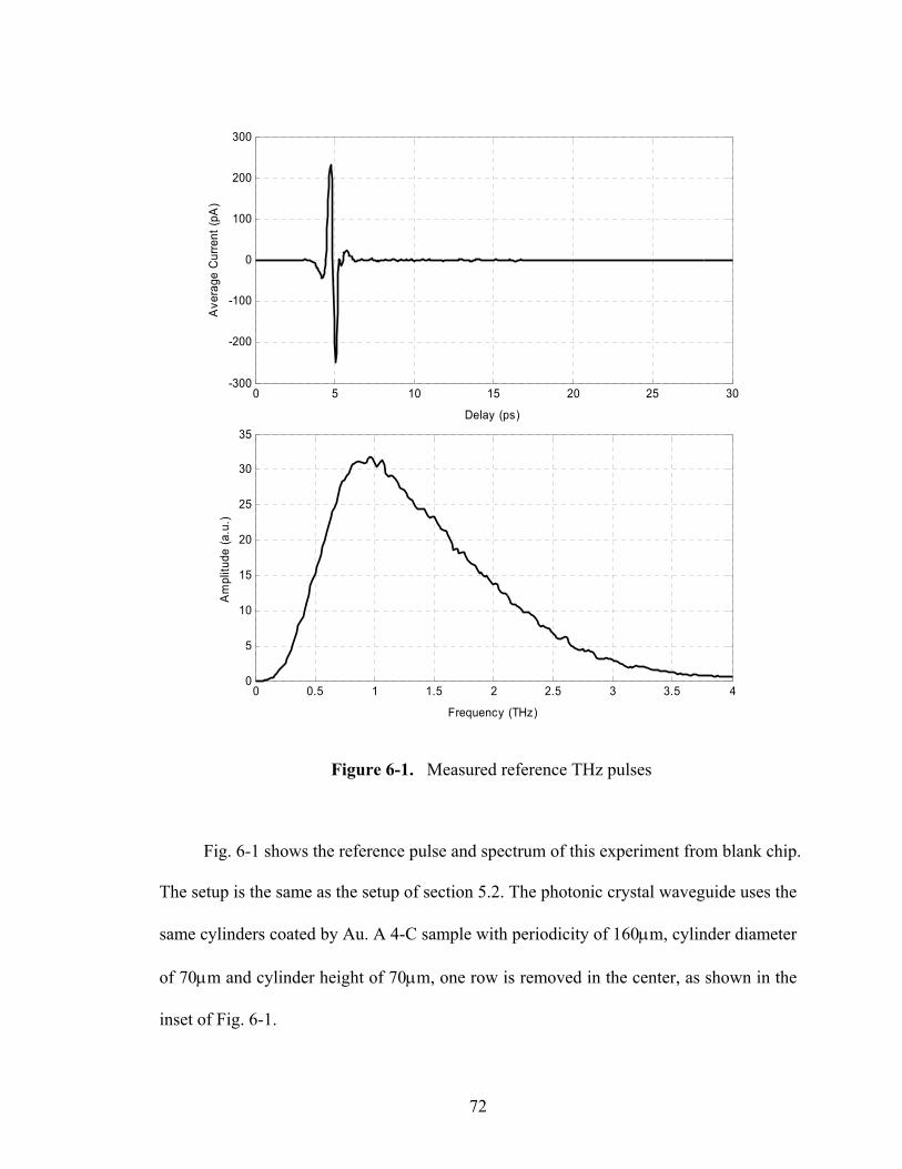
0 5 10 15 20 25 30-300
-200
-100
0
100
200
300
Delay (ps)
Ave
rage
Cur
rent
(pA
)
0 0.5 1 1.5 2 2.5 3 3.5 40
5
10
15
20
25
30
35
Frequency (THz)
Am
plitu
de (a
.u.)
Figure 6-1. Measured reference THz pulses
Fig. 6-1 shows the reference pulse and spectrum of this experiment from blank chip.
The setup is the same as the setup of section 5.2. The photonic crystal waveguide uses the
same cylinders coated by Au. A 4-C sample with periodicity of 160µm, cylinder diameter
of 70µm and cylinder height of 70µm, one row is removed in the center, as shown in the
inset of Fig. 6-1.
72
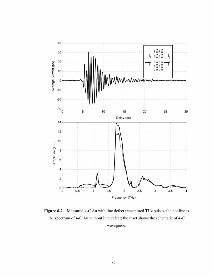
0 5 10 15 20 25 30-30
-20
-10
0
10
20
30
40
Delay (ps)
Ave
rage
Cur
rent
(pA
)
0 0.5 1 1.5 2 2.5 3 3.5 40
2
4
6
8
10
12
14
Frequency (THz)
Am
plitu
de (a
.u.)
Figure 6-2. Measured 4-C Au with line defect transmitted THz pulses, the dot line is
the spectrum of 4-C Au without line defect; the inset shows the schematic of 4-C
waveguide.
73
0 0.5 1 1.5 2 2.5 30
0.1
0.2
0.3
0.4
0.5
0.6
0.7
0.8
Frequency (THz)
Am
plitu
de T
rans
mis
sion
Figure 6-3. Measured amplitude transmission for the 4-C Au with line defect sample
Fig. 6-2 shows the measured pulse and spectrum from the 4-C Au sample with one
line removed. With comparing to the spectrum of 4-C Au without line defect (dot line in
Fig. 6-2), there are some transmission in the first gap from 0.53 to 1.0 THz and the
second gap from 1.2 to 1.5 THz. The amplitude transmission of the sample is shown in
Fig. 6-3, where the transmission between two gaps can be clearly seen.
74
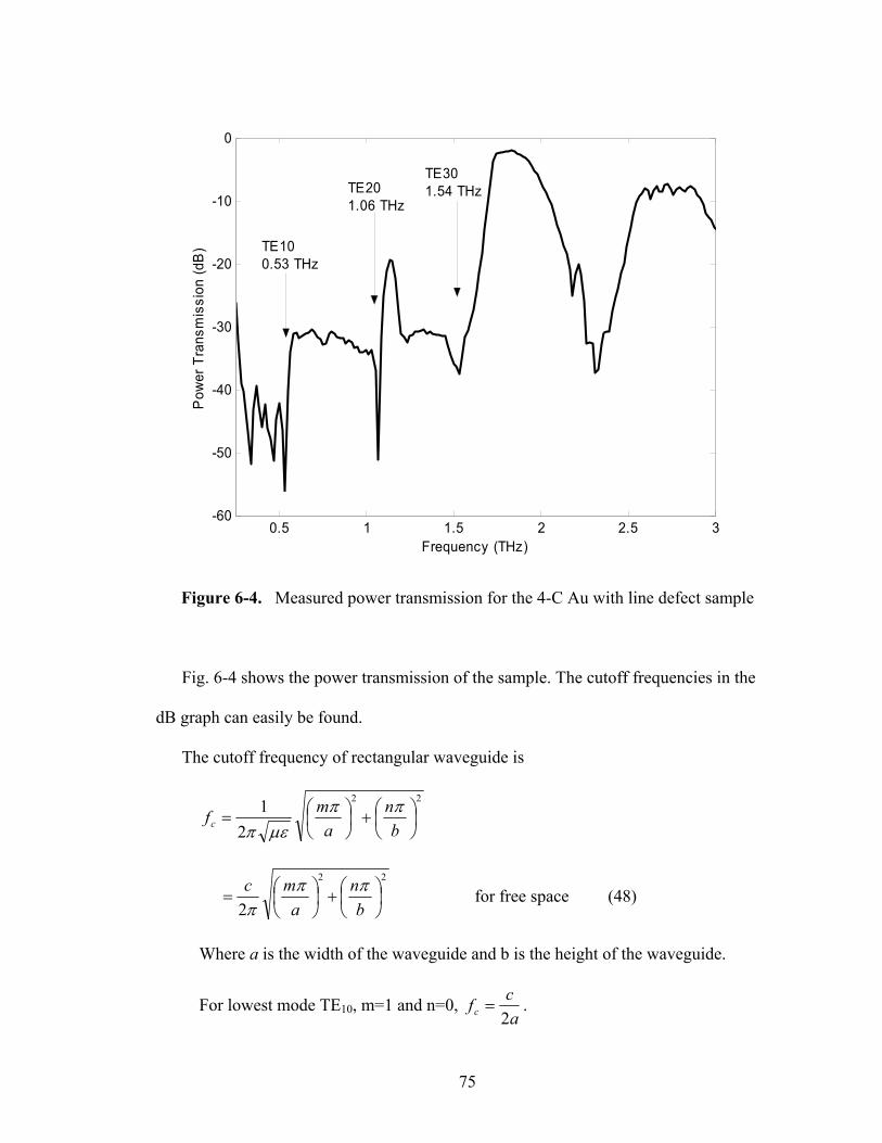
0.5 1 1.5 2 2.5 3-60
-50
-40
-30
-20
-10
0
Frequency (THz)
Pow
er T
rans
mis
sion
(dB
) TE100.53 THz
TE201.06 THz
TE301.54 THz
Figure 6-4. Measured power transmission for the 4-C Au with line defect sample
Fig. 6-4 shows the power transmission of the sample. The cutoff frequencies in the
dB graph can easily be found.
The cutoff frequency of rectangular waveguide is
22
21
⎟⎠⎞
⎜⎝⎛+⎟
⎠⎞
⎜⎝⎛=
bn
amfc
ππµεπ
22
2⎟⎠⎞
⎜⎝⎛+⎟
⎠⎞
⎜⎝⎛=
bn
amc ππ
π for free space (48)
Where a is the width of the waveguide and b is the height of the waveguide.
For lowest mode TE10, m=1 and n=0, acfc 2
= .
75
When one row is removed from the 160µm periodic lattices, the effective width of
photonic crystal waveguide should be between 250µm (the edge to edge of cylinders) and
320µm (the center to center of cylinders). The experimental cutoff frequency is about
0.53 THz. The effective width from the above equation is about 283µm. For 250µm and
320µm, the calculated cutoff frequency is 0.6 THz and 0.47 THz, respectively.
Apparently, the experimental result can be explained by the rectangular waveguide theory
with effective width. Ref. 66 mentions the calculated result is about 0.278(c/a), which
corresponds to 0.52 THz in our case. There also exist dips at 1.06 THz and 1.54 THz,
which correspond to the cutoff frequencies of TE20 and TE30.
We noticed the transmitted power from the waveguide is very weak. The reason of
that is the coupling in THz beam through the plano-cylindrical silicon lens is a line
source instead of a point source. Most of the coupled power is consumed by the standard
4-C photonic crystal structure. The future setup using a spherical silicon lens is under test.
In that case, the point source can couple more power into the waveguide.
6.2 Tunable photonic bandgap realization
It is well known that the photonic crystals have ability that can manipulate the
propagation wave [1, 2, 67]. The most important property of photonic crystals is the
photonic bandgaps. The bandgaps in photonic crystals depend on the periodic pattern,
properties of construction materials, such as the dielectric constants, the plasma
frequencies. Recently, there has been growing interest in the realization of tunable
photonic bandgap, because there are many important applications by using tunable
76
structures, such as filtering, switching and photonic devices. Therefore, many practical
methods are proposed to control the photonic bandgap. These proposals include the
modifying of the external magnetic field [92], the tuning of magnetic permeability [93]
and dielectric permittivity [94], the changing of plasma frequency [95], and the structure
changing of the photonic crystals by strain [96].
Here, we propose an easy method to realize the photonic bandgap tuning by changing
the air gap between the top of the two dimensional (2D) metallic photonic crystal
structures and the cover metal plate, which are bounded in parallel plate waveguide
(PPWG). The bandgap by this way can be controlled from 0.062 THz to 0.918 THz. This
structure can be compared to our early work on the air-spaced, broken-symmetry
photonic PPWG [44], which showed sharp responses in regions as large as 1 THz. For
standard metallic photonic crystals, it has large bandgap, light weight, and smaller size
[4]. These advantages are suit for the photonic device design. For periodic boundary
condition waveguide, the mathematical model can be thought as a cascade connection of
equivalent impedance networks [97]. And the propagated wave depends on these
impedances, which are determined by the physical conditions of the waveguide, such as
the gap distance, periodicity, and so on. With the air gap appearing between the photonic
crystal structures and the cover metal plate, the situation becomes complicated. The
transmitted wave in this case will combine the effects of pure metallic photonic crystal
structures and the effects of the waveguide with periodic boundary conditions, and it is
hard to fit with any existing theory.
77
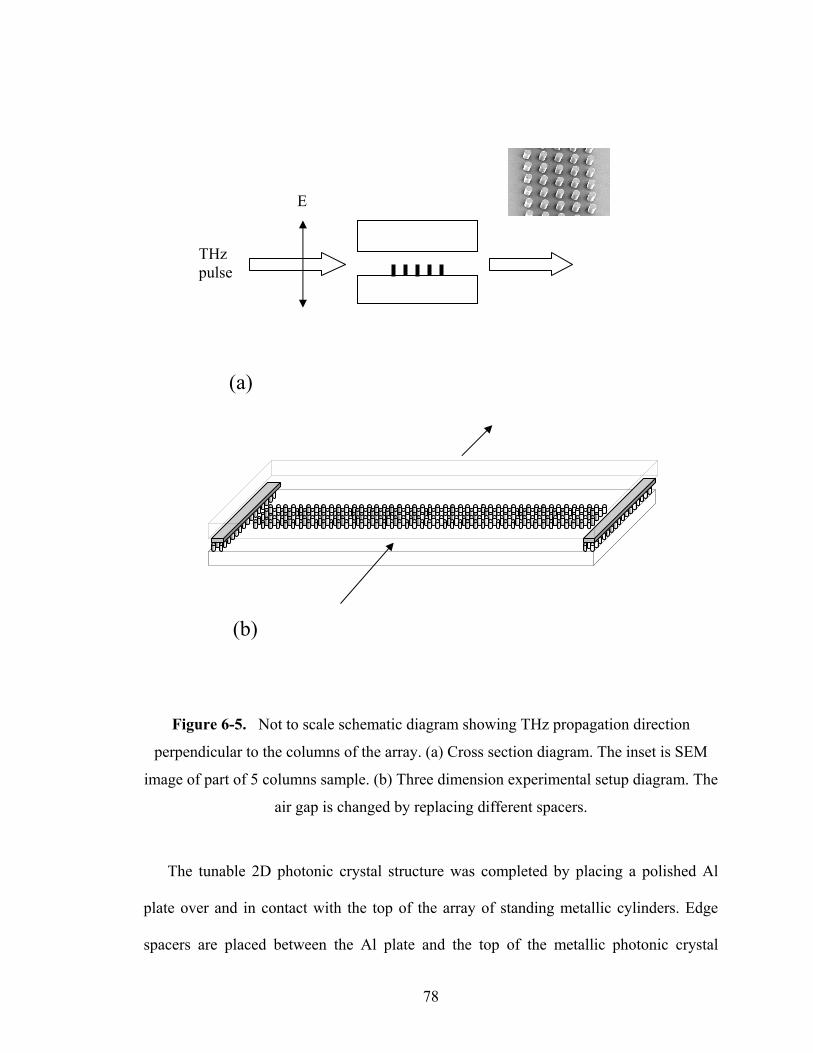
E
THz pulse
(a)
(b)
Figure 6-5. Not to scale schematic diagram showing THz propagation direction
perpendicular to the columns of the array. (a) Cross section diagram. The inset is SEM
image of part of 5 columns sample. (b) Three dimension experimental setup diagram. The
air gap is changed by replacing different spacers.
The tunable 2D photonic crystal structure was completed by placing a polished Al
plate over and in contact with the top of the array of standing metallic cylinders. Edge
spacers are placed between the Al plate and the top of the metallic photonic crystal
78
surface. As shown in Fig. 6-5(a), the THz pulse propagation is perpendicular to the
columns of cylinders in the (10) direction of square pattern with the polarization parallel
to the cylinders. The resulting tunable photonic crystal structure centered within the 10
mm-long PPWG (Fig. 6-5(b)) were characterized by the standard THz-TDS system [8].
Two plano-cylindrical high-resistivity silicon lenses are used to couple the radiation into
and out of the waveguide setup, placed at the confocal beam waist of the THz-TDS
system [84]. The lenses are 15 mm x 10 mm x 6.56 mm with a 5 mm radius of curvature.
The input lens focuses the incoming THz radiation to an elliptical spot with a frequency
independent minor axis of 150µm, perpendicular to the waveguide plates, and a linearly
wavelength-dependent major axis parallel to the plates with a 1/e amplitude diameter d =
9 mm at 1 THz. The THz experimental arrangement converts the incident 3D plane wave
from the THz transmitter into an incident 2D line wave matched to the waveguide and
couples the waveguide output 2D line wave into an outgoing 3D plane wave which is
then efficiently coupled into the THz receiver.
79
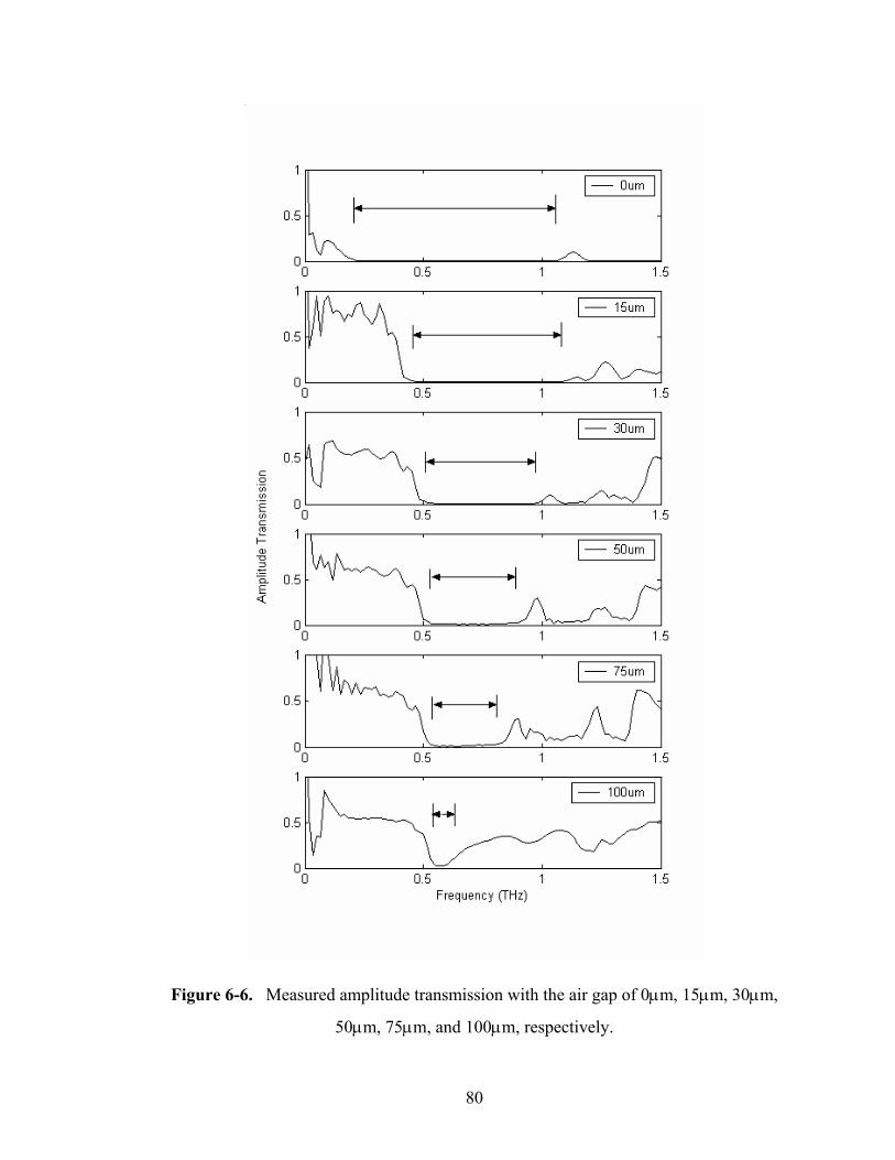
Figure 6-6. Measured amplitude transmission with the air gap of 0µm, 15µm, 30µm,
50µm, 75µm, and 100µm, respectively.
80
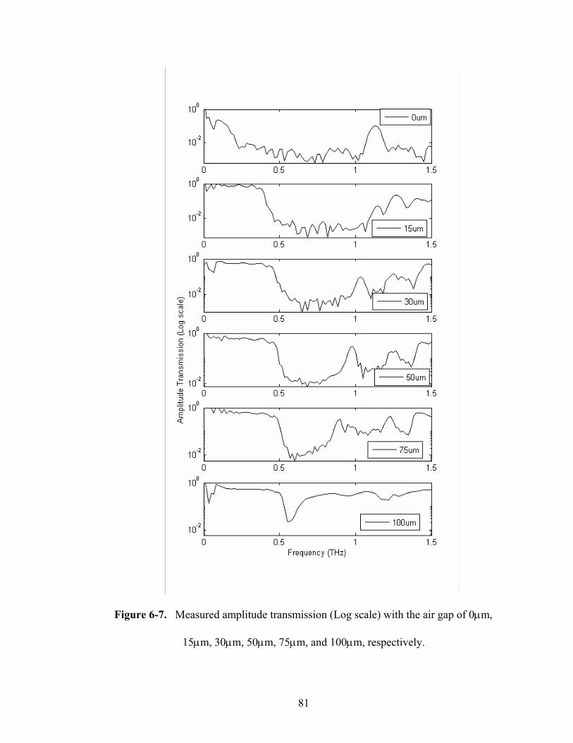
Figure 6-7. Measured amplitude transmission (Log scale) with the air gap of 0µm,
15µm, 30µm, 50µm, 75µm, and 100µm, respectively.
81
Fig. 6-6 shows the amplitude transmissions from 0 to 1.5 THz with the air gap from
0µm to 100µm. The THz reference pulse and spectrum was measured by the standard
PPWG with 80µm air gap, which is the height of the cylinders. The pulses and spectra of
the sample were measured by changing the spacer thickness, 0µm, 15µm, 30µm, 50µm,
75µm, and 100µm, respectively. The amplitude transmissions are achieved by the ratios
of the sample spectrum and the reference spectrum, T(f) = S(f) / R(f), where T(f) is
amplitude transmission, S(f) is sample spectrum and R(f) is reference spectrum. Fig. 6-7
uses log scale to show this bandgap change more clearly. The wave coupled into the
PPWG has single TEM mode because the cutoff frequency of that single mode in PPWG
for maximum couple gap 80µm (columns) + 100µm (air) = 180µm is 1.67 THz [84],
where the maximum frequency 1.5 THz in the measurement is in the single mode range.
This single mode situation enables the capability of the two dimensional structures to
simulate the infinitely long three dimensional structures [86], consisting of two infinitely-
long identical column arrays separated by twice the air gap. Obviously, the first bandgap
shown in Fig. 6-6 and Fig. 6-7 is narrowing and the band edge is changing with
increasing air gap.
82
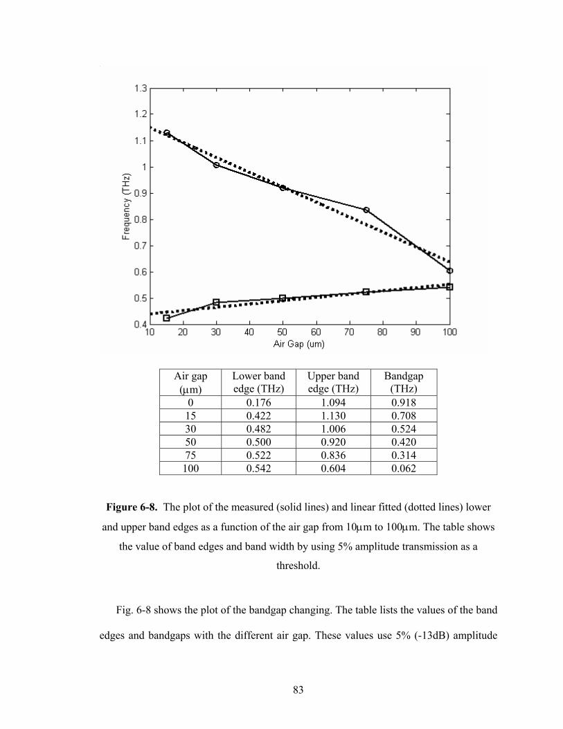
Air gap (µm)
Lower band edge (THz)
Upper band edge (THz)
Bandgap (THz)
0 0.176 1.094 0.918 15 0.422 1.130 0.708 30 0.482 1.006 0.524 50 0.500 0.920 0.420 75 0.522 0.836 0.314 100 0.542 0.604 0.062
Figure 6-8. The plot of the measured (solid lines) and linear fitted (dotted lines) lower
and upper band edges as a function of the air gap from 10µm to 100µm. The table shows
the value of band edges and band width by using 5% amplitude transmission as a
threshold.
Fig. 6-8 shows the plot of the bandgap changing. The table lists the values of the band
edges and bandgaps with the different air gap. These values use 5% (-13dB) amplitude
83
transmission as the threshold, which was selected for comparison conveniently. The
lower and upper band edge plots demonstrate the linear relationship between the air gap
and the frequency. The measured results in solid lines and the linear fit in dotted lines of
Fig. 6-7 indicate the realization of the bandgap tuning. Except the result of the air gap of
0um, the band edge changing is basically linear. The upper band edge drops very fast
from 1.13 THz with 15µm gap to 0.604 THz with 100µm gap. And the lower band edge
raises slowly from 0.422 THz with the 15µm gap to 0.542 THz with 100µm gap. The
total photonic bandgap is changed from 0.708 THz to 0.062 THz.
According to the measurement results, the tunable THz photonic crystal device can be
realized by replacing the edge spacers with the piezoelectric actuators to control the air
gap. With the precise air gap adjustment, the certain bandgap will be achieved. If the
photonic crystal pattern and size are changed, the various bandgap changing speed and
width should be easily observed. It is believable that this tunable structure can apply to
the microwave and optical regime due to the scaling principle.
84
CHAPTER VII
CONCLUSIONS
In this thesis, the concepts of photonic crystals are first introduced. The PWE
approach is the basic method to analyze the band structure of photonic crystals. The
dielectric photonic crystal structures without loss are easy to apply in the PWE method.
For lossy and dispersive materials and more complex structures, FDTD and TMM are
better choices.
Our fabrication capability of making THz chips enables us to apply photonic crystal
structures easily. The integration of the MEMS method and traditional lithography shows
its advantage in making the dielectric and metallic photonic crystal structures. The very
high aspect ratio structures are formed by this approach and the almost ideal properties
are shown in these structures.
We demonstrated the 2D THz polymer (SU-8), which shows the bandgaps from
0.81 to 0.91 THz and 1.5 to 1.84 THz at the (10) incident direction. These effectively 2D
photonic bandgap structures are embedded in THz PPWG setup and show the comparable
results with ideal infinite structures. This experiment demonstrated that the bounded
space between metal PPWG can be used to create physical embodiments of effectively
2D THz TEM-mode propagation experiments. The same setup was also used in metallic
photonic crystal structures, which show wide bandgaps from 0 to 1.0 THz and from 1.1 to
85
1.6 THz. For the point defect and F-P defect photonic structures, the strong localization
(defect modes) are investigated. The experimental results matched the simulation results
very well. The advantages of the single mode PPWG and the quasi-optic coupling
method give us a powerful tool to simulate infinite 2D ideal photonic crystal structures,
and to do further research of THz photonic crystal structures.
Some applications are demonstrated in this thesis. THz metallic photonic crystal
waveguide is tested in the PPWG setup and shows obvious cutoff frequencies which
corresponded to the rectangular metal waveguide. We also report the experimental
realization of a tunable THz photonic bandgap structure. The tunable structure is built
inside the PPWG and operates by changing the air gap, with air gap changing between
the top of the metallic photonic crystal slab and the cover metal plate. The photonic
bandgap can be linearly controlled by adjusting the distance of the air gap. The bandgap
adjustable from 0.062 THz to 0.918 THz is achieved by using this method.
86
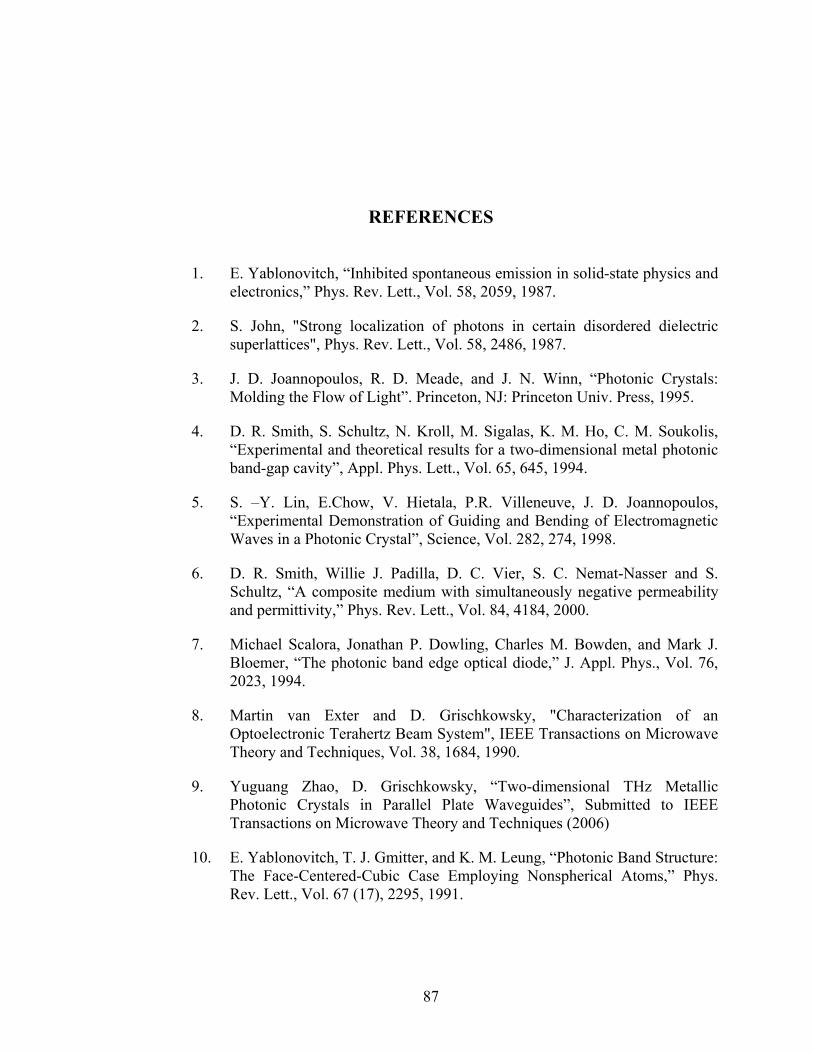
REFERENCES
1. E. Yablonovitch, “Inhibited spontaneous emission in solid-state physics and
electronics,” Phys. Rev. Lett., Vol. 58, 2059, 1987.
2. S. John, "Strong localization of photons in certain disordered dielectric superlattices", Phys. Rev. Lett., Vol. 58, 2486, 1987.
3. J. D. Joannopoulos, R. D. Meade, and J. N. Winn, “Photonic Crystals: Molding the Flow of Light”. Princeton, NJ: Princeton Univ. Press, 1995.
4. D. R. Smith, S. Schultz, N. Kroll, M. Sigalas, K. M. Ho, C. M. Soukolis, “Experimental and theoretical results for a two-dimensional metal photonic band-gap cavity”, Appl. Phys. Lett., Vol. 65, 645, 1994.
5. S. –Y. Lin, E.Chow, V. Hietala, P.R. Villeneuve, J. D. Joannopoulos, “Experimental Demonstration of Guiding and Bending of Electromagnetic Waves in a Photonic Crystal”, Science, Vol. 282, 274, 1998.
6. D. R. Smith, Willie J. Padilla, D. C. Vier, S. C. Nemat-Nasser and S. Schultz, “A composite medium with simultaneously negative permeability and permittivity,” Phys. Rev. Lett., Vol. 84, 4184, 2000.
7. Michael Scalora, Jonathan P. Dowling, Charles M. Bowden, and Mark J. Bloemer, “The photonic band edge optical diode,” J. Appl. Phys., Vol. 76, 2023, 1994.
8. Martin van Exter and D. Grischkowsky, "Characterization of an Optoelectronic Terahertz Beam System", IEEE Transactions on Microwave Theory and Techniques, Vol. 38, 1684, 1990.
9. Yuguang Zhao, D. Grischkowsky, “Two-dimensional THz Metallic Photonic Crystals in Parallel Plate Waveguides”, Submitted to IEEE Transactions on Microwave Theory and Techniques (2006)
10. E. Yablonovitch, T. J. Gmitter, and K. M. Leung, “Photonic Band Structure: The Face-Centered-Cubic Case Employing Nonspherical Atoms,” Phys. Rev. Lett., Vol. 67 (17), 2295, 1991.
87
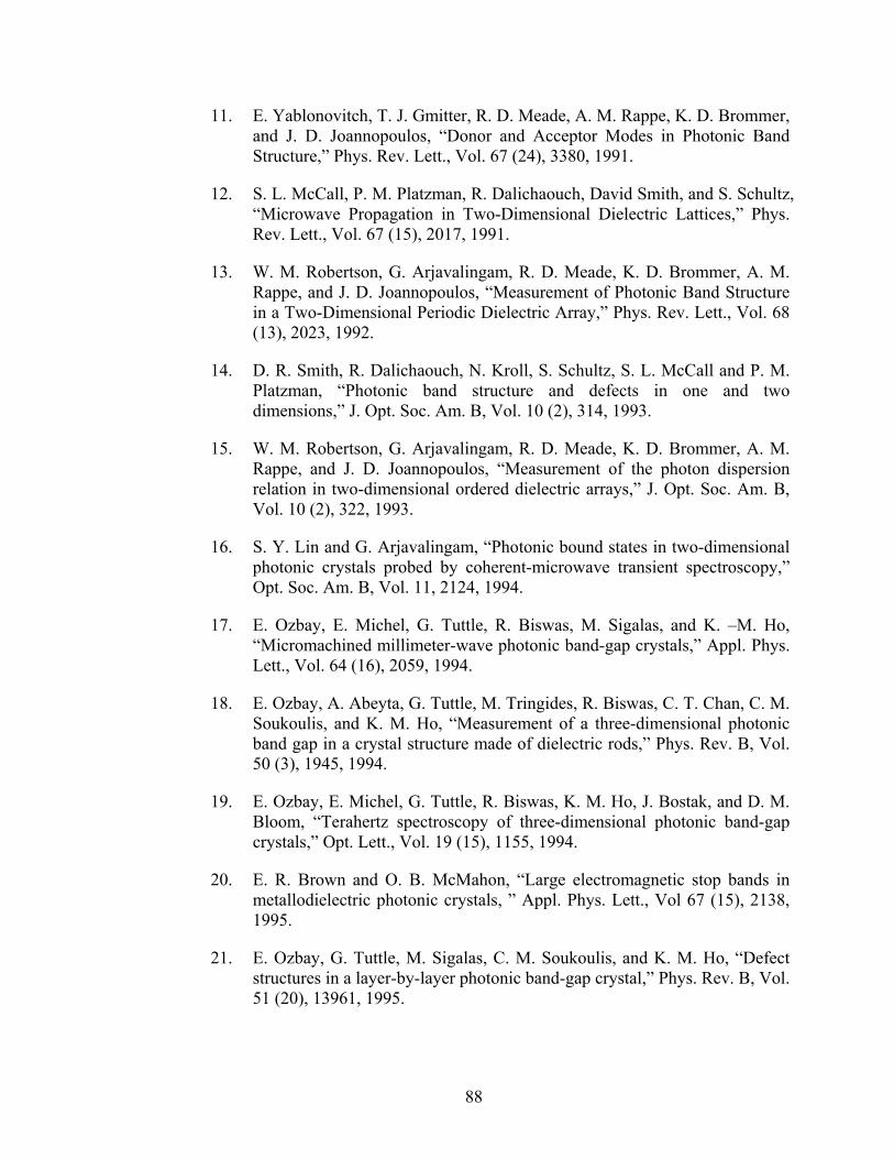
11. E. Yablonovitch, T. J. Gmitter, R. D. Meade, A. M. Rappe, K. D. Brommer, and J. D. Joannopoulos, “Donor and Acceptor Modes in Photonic Band Structure,” Phys. Rev. Lett., Vol. 67 (24), 3380, 1991.
12. S. L. McCall, P. M. Platzman, R. Dalichaouch, David Smith, and S. Schultz, “Microwave Propagation in Two-Dimensional Dielectric Lattices,” Phys. Rev. Lett., Vol. 67 (15), 2017, 1991.
13. W. M. Robertson, G. Arjavalingam, R. D. Meade, K. D. Brommer, A. M. Rappe, and J. D. Joannopoulos, “Measurement of Photonic Band Structure in a Two-Dimensional Periodic Dielectric Array,” Phys. Rev. Lett., Vol. 68 (13), 2023, 1992.
14. D. R. Smith, R. Dalichaouch, N. Kroll, S. Schultz, S. L. McCall and P. M. Platzman, “Photonic band structure and defects in one and two dimensions,” J. Opt. Soc. Am. B, Vol. 10 (2), 314, 1993.
15. W. M. Robertson, G. Arjavalingam, R. D. Meade, K. D. Brommer, A. M. Rappe, and J. D. Joannopoulos, “Measurement of the photon dispersion relation in two-dimensional ordered dielectric arrays,” J. Opt. Soc. Am. B, Vol. 10 (2), 322, 1993.
16. S. Y. Lin and G. Arjavalingam, “Photonic bound states in two-dimensional photonic crystals probed by coherent-microwave transient spectroscopy,” Opt. Soc. Am. B, Vol. 11, 2124, 1994.
17. E. Ozbay, E. Michel, G. Tuttle, R. Biswas, M. Sigalas, and K. –M. Ho, “Micromachined millimeter-wave photonic band-gap crystals,” Appl. Phys. Lett., Vol. 64 (16), 2059, 1994.
18. E. Ozbay, A. Abeyta, G. Tuttle, M. Tringides, R. Biswas, C. T. Chan, C. M. Soukoulis, and K. M. Ho, “Measurement of a three-dimensional photonic band gap in a crystal structure made of dielectric rods,” Phys. Rev. B, Vol. 50 (3), 1945, 1994.
19. E. Ozbay, E. Michel, G. Tuttle, R. Biswas, K. M. Ho, J. Bostak, and D. M. Bloom, “Terahertz spectroscopy of three-dimensional photonic band-gap crystals,” Opt. Lett., Vol. 19 (15), 1155, 1994.
20. E. R. Brown and O. B. McMahon, “Large electromagnetic stop bands in metallodielectric photonic crystals, ” Appl. Phys. Lett., Vol 67 (15), 2138, 1995.
21. E. Ozbay, G. Tuttle, M. Sigalas, C. M. Soukoulis, and K. M. Ho, “Defect structures in a layer-by-layer photonic band-gap crystal,” Phys. Rev. B, Vol. 51 (20), 13961, 1995.
88
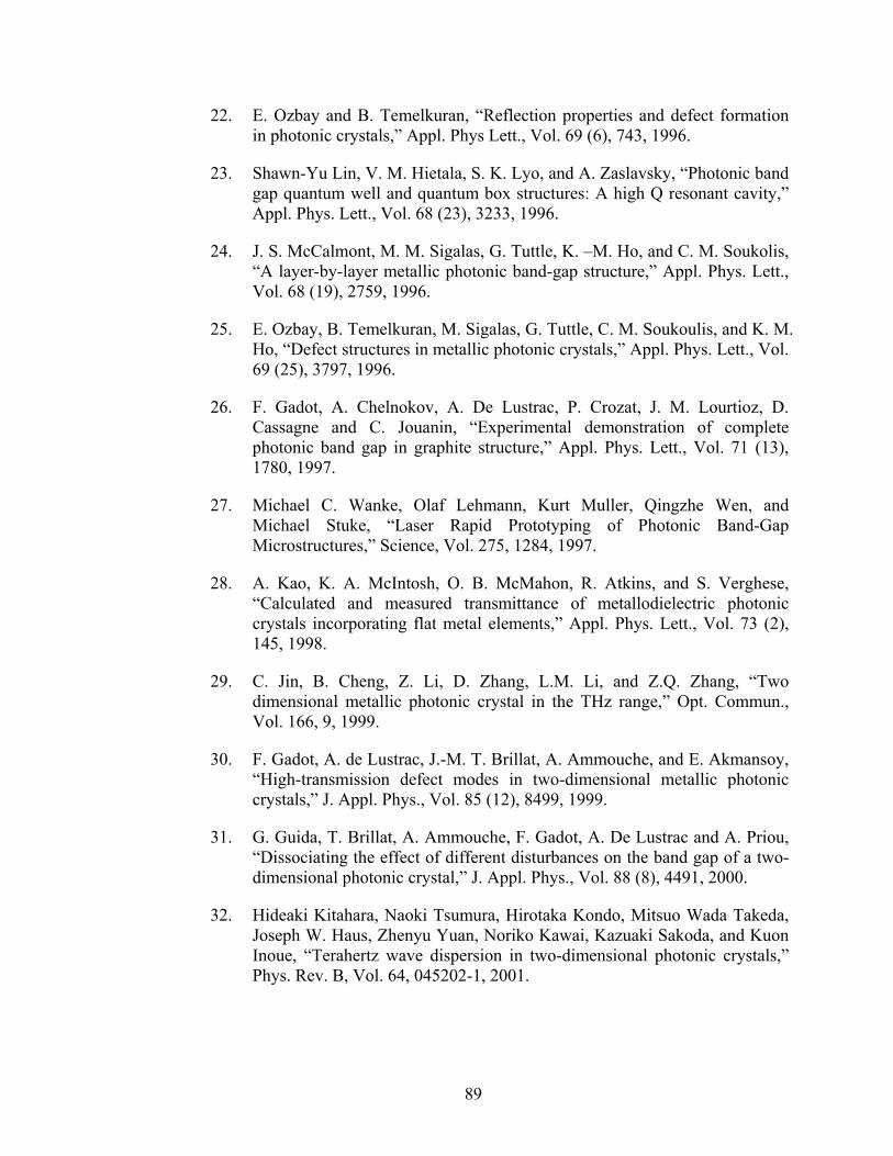
22. E. Ozbay and B. Temelkuran, “Reflection properties and defect formation in photonic crystals,” Appl. Phys Lett., Vol. 69 (6), 743, 1996.
23. Shawn-Yu Lin, V. M. Hietala, S. K. Lyo, and A. Zaslavsky, “Photonic band gap quantum well and quantum box structures: A high Q resonant cavity,” Appl. Phys. Lett., Vol. 68 (23), 3233, 1996.
24. J. S. McCalmont, M. M. Sigalas, G. Tuttle, K. –M. Ho, and C. M. Soukolis, “A layer-by-layer metallic photonic band-gap structure,” Appl. Phys. Lett., Vol. 68 (19), 2759, 1996.
25. E. Ozbay, B. Temelkuran, M. Sigalas, G. Tuttle, C. M. Soukoulis, and K. M. Ho, “Defect structures in metallic photonic crystals,” Appl. Phys. Lett., Vol. 69 (25), 3797, 1996.
26. F. Gadot, A. Chelnokov, A. De Lustrac, P. Crozat, J. M. Lourtioz, D. Cassagne and C. Jouanin, “Experimental demonstration of complete photonic band gap in graphite structure,” Appl. Phys. Lett., Vol. 71 (13), 1780, 1997.
27. Michael C. Wanke, Olaf Lehmann, Kurt Muller, Qingzhe Wen, and Michael Stuke, “Laser Rapid Prototyping of Photonic Band-Gap Microstructures,” Science, Vol. 275, 1284, 1997.
28. A. Kao, K. A. McIntosh, O. B. McMahon, R. Atkins, and S. Verghese, “Calculated and measured transmittance of metallodielectric photonic crystals incorporating flat metal elements,” Appl. Phys. Lett., Vol. 73 (2), 145, 1998.
29. C. Jin, B. Cheng, Z. Li, D. Zhang, L.M. Li, and Z.Q. Zhang, “Two dimensional metallic photonic crystal in the THz range,” Opt. Commun., Vol. 166, 9, 1999.
30. F. Gadot, A. de Lustrac, J.-M. T. Brillat, A. Ammouche, and E. Akmansoy, “High-transmission defect modes in two-dimensional metallic photonic crystals,” J. Appl. Phys., Vol. 85 (12), 8499, 1999.
31. G. Guida, T. Brillat, A. Ammouche, F. Gadot, A. De Lustrac and A. Priou, “Dissociating the effect of different disturbances on the band gap of a two-dimensional photonic crystal,” J. Appl. Phys., Vol. 88 (8), 4491, 2000.
32. Hideaki Kitahara, Naoki Tsumura, Hirotaka Kondo, Mitsuo Wada Takeda, Joseph W. Haus, Zhenyu Yuan, Noriko Kawai, Kazuaki Sakoda, and Kuon Inoue, “Terahertz wave dispersion in two-dimensional photonic crystals,” Phys. Rev. B, Vol. 64, 045202-1, 2001.
89
33. B. Temelkuran, Mehmet Beyindir, E. Ozbay, J. P. Kavanaugh, M. M. Sigalas and G. Tuttle, “Quasimetallic silicon micromachined photonic crystals,” Appl. Phys. Lett., Vol. 78 (3), 264, 2001.
34. Mehmet Bayindir, E. Cubukcu, I. Bulu, T. Tut, E. Ozbay, and C. M. Soukoulis, “Photonic band gaps, defect characteristics, and waveguiding in two-dimensional disordered dielectric and metallic photonic crystals,” Phys. Rev. B, Vol. 64, 195113-1, 2001.
35. N. Katsarakis, M. Bender, L. Singleton, G. Kiriakidis and C. M. Soukoulis, “Two-dimensional metallic photonic band-gap crystals fabricated by LIGA,” Microsystem Tech., Vol. 8, 74, 2002.
36. Ali Serpenguzel, “Transmission Characteristics of Metallodielectric Photonic Crystals and Resonators,” IEEE Microwave and Wireless Components Letters, Vol. 12 (4), 134, 2002.
37. Philippe Gay-Balmaz, Claudio Maccio, and Olivier J. F. Martin, “Microwire arrays with plasmonic response at microwave frequencies,” Appl. Phys. Lett., Vol. 81 (15), 2896, 2002.
38. Shao-Wei Wang, Wei Lu, Xiao-Shuang Chen, Zhi-Feng Li, Xue-Chu Shen, and Weijia Wen, “Two-dimensional photonic crystal at THz frequencies constructed by metal-coated cylinders,” J. of Appl. Phys., Vol. 93 (11), 9401, 2003.
39. Dongmin Wu, Nicholas Fang, Cheng Sun, and Xiang Zhang, Willie J. Padilla, Dimitri N. Basov, David R. Smith, and Sheldon Schultz, “Terahertz plasmonic high pass filter,” Appl. Phys. Lett., Vol. 83 (1), 201, 2003.
40. Nathan Jukam and Mark S. Sherwin, “Two-dimensional terahertz photonic crystals fabricated by deep reactive ion etching in Si,” Appl. Phys. Lett., Vol. 83 (1), 21, 2003.
41. Timothy D. Drysdale, Richard J. Blaikie, and David R. S. Cumming, “Calculated and measured transmittance of a tunable metallic photonic crystal filter for terahertz frequencies,” Appl. Phys. Lett., Vol. 83 (26), 5362, 2003.
42. Z. Jian, J. Pearce, and D. Mittleman, “Defect modes in photonic crystal slabs studied using terahertz time-domain spectroscopy,” Opt. Lett., Vol. 29 (17), 2067, 2004.
43. M. Golosovsky, Y. Neve-Oz, D. Davidov, and A. Frenkel, “Phase shift on reflection from metallodielectric photonic bandgap materials,” Phys. Rev. B, Vol. 70, 115105-1, 2004.
90
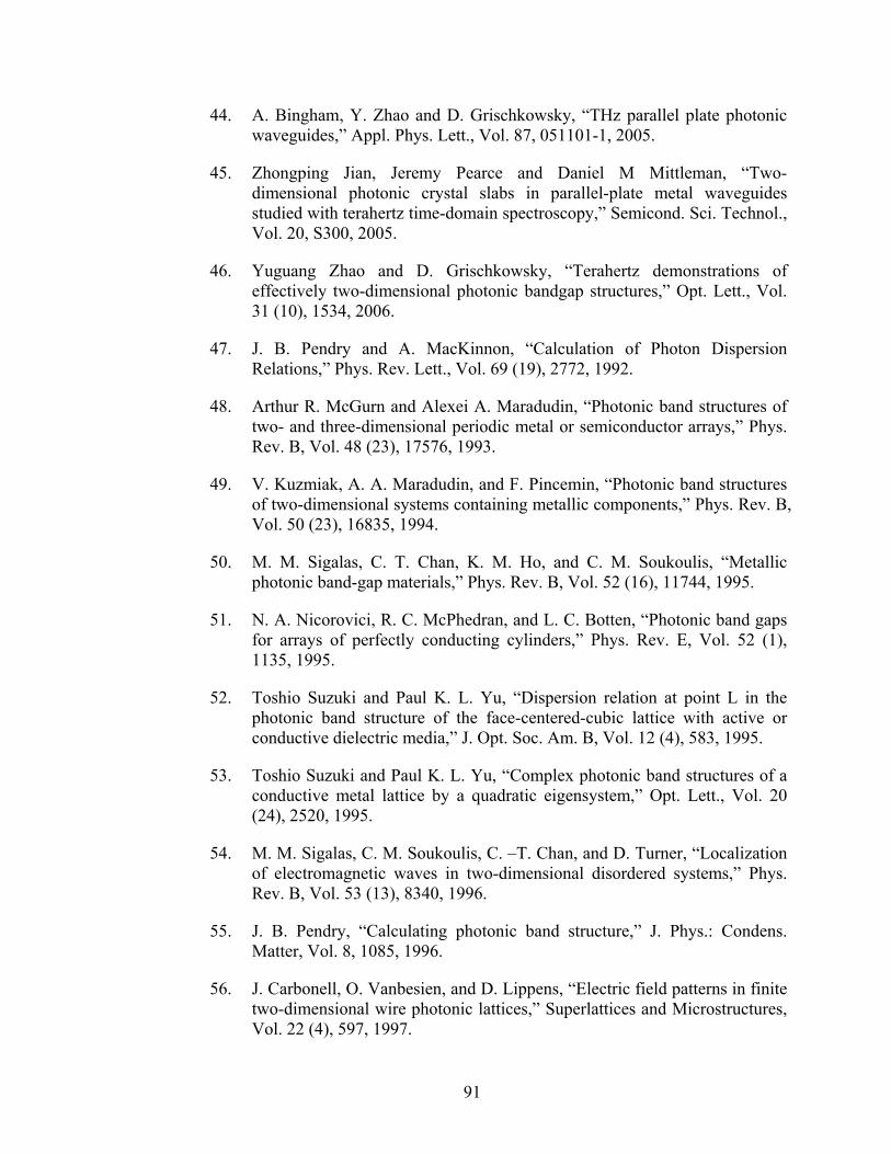
44. A. Bingham, Y. Zhao and D. Grischkowsky, “THz parallel plate photonic waveguides,” Appl. Phys. Lett., Vol. 87, 051101-1, 2005.
45. Zhongping Jian, Jeremy Pearce and Daniel M Mittleman, “Two-dimensional photonic crystal slabs in parallel-plate metal waveguides studied with terahertz time-domain spectroscopy,” Semicond. Sci. Technol., Vol. 20, S300, 2005.
46. Yuguang Zhao and D. Grischkowsky, “Terahertz demonstrations of effectively two-dimensional photonic bandgap structures,” Opt. Lett., Vol. 31 (10), 1534, 2006.
47. J. B. Pendry and A. MacKinnon, “Calculation of Photon Dispersion Relations,” Phys. Rev. Lett., Vol. 69 (19), 2772, 1992.
48. Arthur R. McGurn and Alexei A. Maradudin, “Photonic band structures of two- and three-dimensional periodic metal or semiconductor arrays,” Phys. Rev. B, Vol. 48 (23), 17576, 1993.
49. V. Kuzmiak, A. A. Maradudin, and F. Pincemin, “Photonic band structures of two-dimensional systems containing metallic components,” Phys. Rev. B, Vol. 50 (23), 16835, 1994.
50. M. M. Sigalas, C. T. Chan, K. M. Ho, and C. M. Soukoulis, “Metallic photonic band-gap materials,” Phys. Rev. B, Vol. 52 (16), 11744, 1995.
51. N. A. Nicorovici, R. C. McPhedran, and L. C. Botten, “Photonic band gaps for arrays of perfectly conducting cylinders,” Phys. Rev. E, Vol. 52 (1), 1135, 1995.
52. Toshio Suzuki and Paul K. L. Yu, “Dispersion relation at point L in the photonic band structure of the face-centered-cubic lattice with active or conductive dielectric media,” J. Opt. Soc. Am. B, Vol. 12 (4), 583, 1995.
53. Toshio Suzuki and Paul K. L. Yu, “Complex photonic band structures of a conductive metal lattice by a quadratic eigensystem,” Opt. Lett., Vol. 20 (24), 2520, 1995.
54. M. M. Sigalas, C. M. Soukoulis, C. –T. Chan, and D. Turner, “Localization of electromagnetic waves in two-dimensional disordered systems,” Phys. Rev. B, Vol. 53 (13), 8340, 1996.
55. J. B. Pendry, “Calculating photonic band structure,” J. Phys.: Condens. Matter, Vol. 8, 1085, 1996.
56. J. Carbonell, O. Vanbesien, and D. Lippens, “Electric field patterns in finite two-dimensional wire photonic lattices,” Superlattices and Microstructures, Vol. 22 (4), 597, 1997.
91
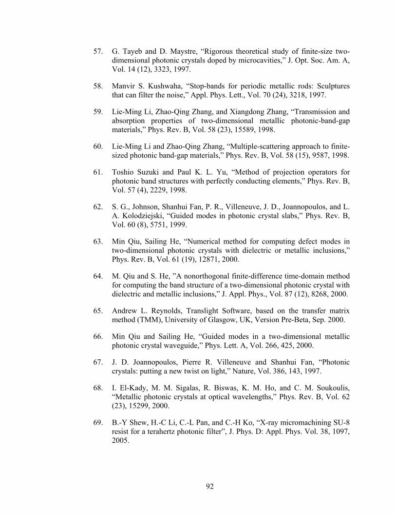
57. G. Tayeb and D. Maystre, “Rigorous theoretical study of finite-size two-dimensional photonic crystals doped by microcavities,” J. Opt. Soc. Am. A, Vol. 14 (12), 3323, 1997.
58. Manvir S. Kushwaha, “Stop-bands for periodic metallic rods: Sculptures that can filter the noise,” Appl. Phys. Lett., Vol. 70 (24), 3218, 1997.
59. Lie-Ming Li, Zhao-Qing Zhang, and Xiangdong Zhang, “Transmission and absorption properties of two-dimensional metallic photonic-band-gap materials,” Phys. Rev. B, Vol. 58 (23), 15589, 1998.
60. Lie-Ming Li and Zhao-Qing Zhang, “Multiple-scattering approach to finite-sized photonic band-gap materials,” Phys. Rev. B, Vol. 58 (15), 9587, 1998.
61. Toshio Suzuki and Paul K. L. Yu, “Method of projection operators for photonic band structures with perfectly conducting elements,” Phys. Rev. B, Vol. 57 (4), 2229, 1998.
62. S. G., Johnson, Shanhui Fan, P. R., Villeneuve, J. D., Joannopoulos, and L. A. Kolodziejski, “Guided modes in photonic crystal slabs,” Phys. Rev. B, Vol. 60 (8), 5751, 1999.
63. Min Qiu, Sailing He, “Numerical method for computing defect modes in two-dimensional photonic crystals with dielectric or metallic inclusions,” Phys. Rev. B, Vol. 61 (19), 12871, 2000.
64. M. Qiu and S. He, ”A nonorthogonal finite-difference time-domain method for computing the band structure of a two-dimensional photonic crystal with dielectric and metallic inclusions,” J. Appl. Phys., Vol. 87 (12), 8268, 2000.
65. Andrew L. Reynolds, Translight Software, based on the transfer matrix method (TMM), University of Glasgow, UK, Version Pre-Beta, Sep. 2000.
66. Min Qiu and Sailing He, “Guided modes in a two-dimensional metallic photonic crystal waveguide,” Phys. Lett. A, Vol. 266, 425, 2000.
67. J. D. Joannopoulos, Pierre R. Villeneuve and Shanhui Fan, “Photonic crystals: putting a new twist on light,” Nature, Vol. 386, 143, 1997.
68. I. El-Kady, M. M. Sigalas, R. Biswas, K. M. Ho, and C. M. Soukoulis, “Metallic photonic crystals at optical wavelengths,” Phys. Rev. B, Vol. 62 (23), 15299, 2000.
69. B.-Y Shew, H.-C Li, C.-L Pan, and C.-H Ko, “X-ray micromachining SU-8 resist for a terahertz photonic filter”, J. Phys. D: Appl. Phys. Vol. 38, 1097, 2005.
92
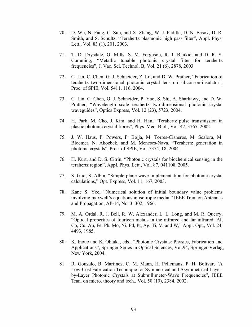
70. D. Wu, N. Fang, C. Sun, and X. Zhang, W. J. Padilla, D. N. Basov, D. R. Smith, and S. Schultz, “Terahertz plasmonic high pass filter”, Appl. Phys. Lett., Vol. 83 (1), 201, 2003.
71. T. D. Drysdale, G. Mills, S. M. Ferguson, R. J. Blaikie, and D. R. S. Cumming, “Metallic tunable photonic crystal filter for terahertz frequencies”, J. Vac. Sci. Technol. B, Vol. 21 (6), 2878, 2003.
72. C. Lin, C. Chen, G. J. Schneider, Z. Lu, and D. W. Prather, “Fabrication of terahertz two-dimensional photonic crystal lens on silicon-on-insulator”, Proc. of SPIE, Vol. 5411, 116, 2004.
73. C. Lin, C. Chen, G. J. Schneider, P. Yao, S. Shi, A. Sharkawy, and D. W. Prather, “Wavelength scale terahertz two-dimensional photonic crystal waveguides”, Optics Express, Vol. 12 (23), 5723, 2004.
74. H. Park, M. Cho, J. Kim, and H. Han, “Terahertz pulse transmission in plastic photonic crystal fibres”, Phys. Med. Biol., Vol. 47, 3765, 2002.
75. J. W. Haus, P. Powers, P. Bojja, M. Torres-Cisneros, M. Scalora, M. Bloemer, N. Akozbek, and M. Meneses-Nava, “Terahertz generation in photonic crystals”, Proc. of SPIE, Vol. 5354, 18, 2004.
76. H. Kurt, and D. S. Citrin, “Photonic crystals for biochemical sensing in the terahertz region”, Appl. Phys. Lett., Vol. 87, 041108, 2005.
77. S. Guo, S. Albin, “Simple plane wave implementation for photonic crystal calculations,” Opt. Express, Vol. 11, 167, 2003.
78. Kane S. Yee, “Numerical solution of initial boundary value problems involving maxwell’s equations in isotropic media,” IEEE Tran. on Antennas and Propagation, AP-14, No. 3, 302, 1966.
79. M. A. Ordal, R. J. Bell, R. W. Alexander, L. L. Long, and M. R. Querry, “Optical properties of fourteen metals in the infrared and far infrared: Al, Co, Cu, Au, Fe, Pb, Mo, Ni, Pd, Pt, Ag, Ti, V, and W,” Appl. Opt., Vol. 24, 4493, 1985.
80. K. Inoue and K. Ohtaka, eds., “Photonic Crystals: Physics, Fabrication and Applications”, Springer Series in Optical Sciences, Vol.94, Springer-Verlag, New York, 2004.
81. R. Gonzalo, B. Martinez, C. M. Mann, H. Pellemans, P. H. Bolivar, “A Low-Cost Fabrication Technique for Symmetrical and Asymmetrical Layer-by-Layer Photonic Crystals at Submillimeter-Wave Frequencies”, IEEE Tran. on micro. theory and tech., Vol. 50 (10), 2384, 2002.
93
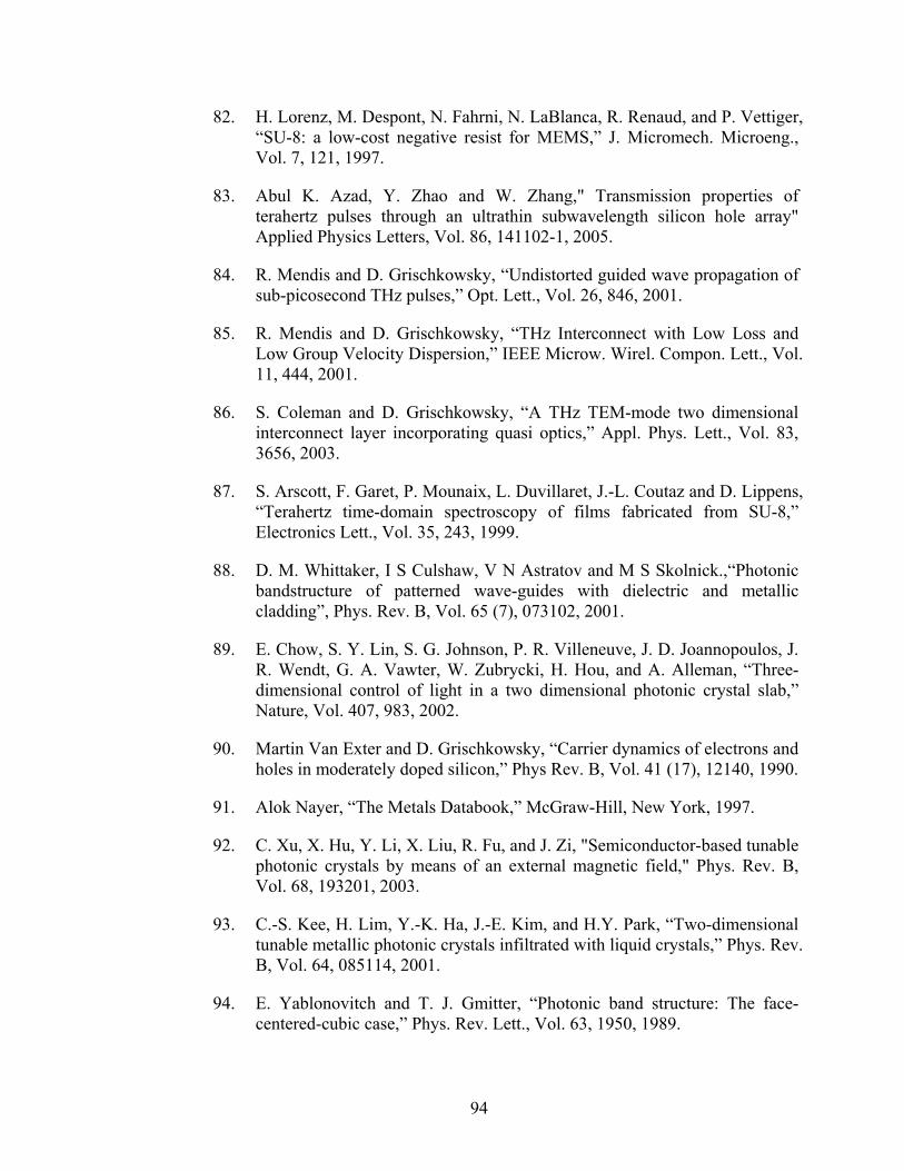
82. H. Lorenz, M. Despont, N. Fahrni, N. LaBlanca, R. Renaud, and P. Vettiger, “SU-8: a low-cost negative resist for MEMS,” J. Micromech. Microeng., Vol. 7, 121, 1997.
83. Abul K. Azad, Y. Zhao and W. Zhang," Transmission properties of terahertz pulses through an ultrathin subwavelength silicon hole array" Applied Physics Letters, Vol. 86, 141102-1, 2005.
84. R. Mendis and D. Grischkowsky, “Undistorted guided wave propagation of sub-picosecond THz pulses,” Opt. Lett., Vol. 26, 846, 2001.
85. R. Mendis and D. Grischkowsky, “THz Interconnect with Low Loss and Low Group Velocity Dispersion,” IEEE Microw. Wirel. Compon. Lett., Vol. 11, 444, 2001.
86. S. Coleman and D. Grischkowsky, “A THz TEM-mode two dimensional interconnect layer incorporating quasi optics,” Appl. Phys. Lett., Vol. 83, 3656, 2003.
87. S. Arscott, F. Garet, P. Mounaix, L. Duvillaret, J.-L. Coutaz and D. Lippens, “Terahertz time-domain spectroscopy of films fabricated from SU-8,” Electronics Lett., Vol. 35, 243, 1999.
88. D. M. Whittaker, I S Culshaw, V N Astratov and M S Skolnick.,“Photonic bandstructure of patterned wave-guides with dielectric and metallic cladding”, Phys. Rev. B, Vol. 65 (7), 073102, 2001.
89. E. Chow, S. Y. Lin, S. G. Johnson, P. R. Villeneuve, J. D. Joannopoulos, J. R. Wendt, G. A. Vawter, W. Zubrycki, H. Hou, and A. Alleman, “Three-dimensional control of light in a two dimensional photonic crystal slab,” Nature, Vol. 407, 983, 2002.
90. Martin Van Exter and D. Grischkowsky, “Carrier dynamics of electrons and holes in moderately doped silicon,” Phys Rev. B, Vol. 41 (17), 12140, 1990.
91. Alok Nayer, “The Metals Databook,” McGraw-Hill, New York, 1997.
92. C. Xu, X. Hu, Y. Li, X. Liu, R. Fu, and J. Zi, "Semiconductor-based tunable photonic crystals by means of an external magnetic field," Phys. Rev. B, Vol. 68, 193201, 2003.
93. C.-S. Kee, H. Lim, Y.-K. Ha, J.-E. Kim, and H.Y. Park, “Two-dimensional tunable metallic photonic crystals infiltrated with liquid crystals,” Phys. Rev. B, Vol. 64, 085114, 2001.
94. E. Yablonovitch and T. J. Gmitter, “Photonic band structure: The face-centered-cubic case,” Phys. Rev. Lett., Vol. 63, 1950, 1989.
94
95. M. S. Kushwaha and B. Djafari-Rouhani, “Band-gap engineering in two-dimensional periodic photonic crystals,” J. Appl. Phys., Vol. 88, 2877, 2000.
96. S. Kim and V. Gopalan, “Strain-tunable photonic band gap crystals,” Appl. Phys. Lett., Vol. 78, 3015, 2001.
97. R. E. Collin, “Field Theory of Guided Waves”, Ch. 9, IEEE press, 1991.
95
VITA
Yuguang Zhao
Candidate for the Degree of
Doctor of Philosophy
Thesis: STUDY OF PHOTONIC CRYSTAL STRUCTURES BY THz-TDS
Major Field: Electrical Engineering Biography:
Personal Data: Born in Chongqing, China, son of Zexun Zhao and Huixiang Tan.
Education: Received the Bachelor of Science degree in Detection Techniques and Instruments from Northwest Polytechnic University, China, in July 1993; and received Master of Science degree in Multidisciplinary Science from Rensselaer Polytechnic Institute, Troy, NY, in August 2002. Completed the requirements for the Doctor of Philosophy of Science degree with a major in Electrical Engineering at Oklahoma State University in December 2006.
Experiences: Employed by Chongqing Sichuan Instrument Co., Ltd., China, as an
electrical engineer, 1993 to 2001; employed by Rensselaer Polytechnic Institute, Department of Physics as a research assistant, 2001 to 2002; employed by Oklahoma State University, Department of Electrical Engineering as a research assistant, 2003 to present.
Name: Yuguang Zhao Date of Degree: December, 2006 Institution: Oklahoma State University Location: Stillwater, Oklahoma Title of Study: STUDY OF PHOTONIC CRYSTAL STRUCTURES BY THz-TDS Pages in Study: 95 Candidate for the Degree of Doctor of Philosophy Major Field: Electrical Engineering Scope and Method of Study: The purpose of this study was to examine the behavior of
dielectric and metallic photonic crystal structures embedded in single mode metal parallel plate waveguide (PPWG). The terahertz (THz) pulse was coupled in and out by two plano-cylindrical silicon lenses. The photonic crystals were fabricated by using Micro-Electro-Mechanical-Systems (MEMS) technology, which constructed very high aspect ratio structures. The transmission properties of the THz radiation of these structures were investigated using terahertz time-domain spectroscopy (THz-TDS).
Findings and Conclusions: We demonstrated the transmitted THz bandgaps in the 2D
polymer (SU-8) photonic crystal structures, 2D metallic photonic crystal structures and 2D metallic photonic crystal defect structures. The experimental results matched the transfer matrix method (TMM) and the finite difference time domain (FDTD) simulation results very well. A very important conclusion is that the advantages of single mode PPWG and the coupling method give us a powerful tool to simulate infinite 2D ideal photonic crystal structures. This method can be used to do the farther research of THz photonic crystal structures. Some applications such as photonic crystal waveguide and tunable photonic bandgap are also investigated and demonstrated.
ADVISER’S APPROVAL: Dr. Daniel Grischkowsky .